1
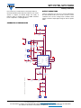
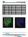
SiP12107DB, SiP12108DB
www.vishay.com
Vishay Siliconix
Demo Board User Manual for SiP12107 (3 A) and SiP12108 (5 A),
2.7 V to 5.5 V Synchronous Buck Regulators
THE CHIP
DESCRIPTION
FEATURES
The SiP12107/SiP12108 is a high frequency current-mode
constant on-time (CM-COT) synchronous buck regulator
with integrated high-side and low-side power MOSFETs. Its
power stage is capable of supplying 5 A (3 A for the
SiP12107) continuous current at 4 MHz switching
frequency. This regulator produces an adjustable output
voltage down to 0.6 V from a 2.8 V to 5.5 V input rail
to accommodate a variety of applications, including
computing, consumer electronics, telecom, and industrial.
• 2.8 V to 5.5 V input voltage
SiP12107/SiP12108's CM-COT architecture delivers
ultra-fast transient response with minimum output
capacitance and tight ripple regulation at very light load. The
part is stable with any capacitor type and no ESR network is
required for loop stability. The device also incorporates a
power saving scheme that significantly increases light
load efficiency. The SiP12107/SiP12108 integrates a full
protection feature set, including output overvoltage
protection (OVP), output undervoltage protection (UVP) and
thermal shutdown (OTP). The “A” version of the 5 A device,
the SiP12108A, does not have the UVP feature. The devices
also incorporate UVLO for the input rail and an internal
soft-start ramp.
The SiP12107/SiP12108/SiP12108A are available in a lead
(Pb)-free power enhanced 3 mm x 3 mm QFN-16 package.
• Adjustable output voltage down to 0.6 V
• 3 A continuous output current for SiP12107
• 5 A continuous output current for SiP12108A
• Programmable switching frequency up to 4 MHz
• 95 % peak efficiency
• Stable with any capacitor. No external ESR network
required
• Ultrafast transient response
• Selectable power
continuous mode
saving
(PSM)
mode
or
forced
• ± 1 % accuracy of VOUT setting
• Pulse-by-pulse current limit
• SiP12107 / SiP12108 is fully protected with OTP, SCP,
UVP, OVP
• SiP12108A is fully protected with OTP, SCP, OVP
• PGOOD indicator
• PowerCAD simulation software available at
www.vishay.transim.com/login.aspx
• Material categorization: For definitions of compliance
please see www.vishay.com/doc?99912
APPLICATIONS
Point of load regulation for low-power processors, network
processors, DSPs, FPGAs, and ASICs
• Low voltage, distributed power architectures with 3.3 V or
5 V rails
• Computing, broadband, networking, LAN/WAN, optical,
test and measurement
• A/V, high density cards, storage, DSL, STB, DVR, DTV,
Industrial PC
ORDERING INFORMATION
DEMO BOARD PART NUMBER
Revision: 22-Jan-14
MAX. OUTPUT CURRENT
SiP12107DB
3A
SiP12108DB
5A
Document Number: 62924
1
For technical questions, contact: [email protected]
THIS DOCUMENT IS SUBJECT TO CHANGE WITHOUT NOTICE. THE PRODUCTS DESCRIBED HEREIN AND THIS DOCUMENT
ARE SUBJECT TO SPECIFIC DISCLAIMERS, SET FORTH AT www.vishay.com/doc?91000
SiP12107DB, SiP12108DB
www.vishay.com
Vishay Siliconix
POWER UP PROCEDURE
CHANGING SWITCHING FREQUENCY
This reference board allows the end user to evaluate
the SiP12107/SiP12108 chip for its features and all
functionalities. It can also be a reference design for a user's
application.
To turn-on the reference board, apply a voltage between
2.8 V and 5.5 V to VIN and EN pins, the board will come up
in PWM mode with an output voltage preset to 1.8 V. To
disable the part, tie the EN pin to GND. To set the part into
power save mode, tie the AUTO pin to GND. This will allow
much higher efficiency due to a very lower switching
frequency at very light loads. As the load increases the
frequency will increase until the nominal set frequency
(preset to ~1 MHz) is reached. PGOOD indicator can be
probed from PGOOD pin.
The following equation illustrates the relationship between
ON-time, VIN, VOUT and RON value:
V
tON = RON x K x OUT
VIN
where K is a constant set internally (K = 10.45 x 10⁻¹²).
Once ON time is set, pseudo constant frequency is then
determined by the following equation:
Fsw =
D
tON
=
VOUT
VIN
VOUT
x RON x K
VIN
1
=
RON x K
SPECIFICATION
OUTPUT RIPPLE VOLTAGE
Input voltage : 2.8 V to 5.5 V
Output voltage: 0.6 V to 3.3 V
Output ripple voltage can be measured across J2 and J3,
but it is better to use a tip and barrel measurement since the
ripple will be very small. Typically output ripple voltage is set
to 3 % to 5 % of the output voltage, with an all ceramic
output solution the output ripple can be very small. Voltage
mode based COT controllers will have stability issues with
an all ceramic solution, because they require the ripple
voltage to provide the ramp needed by the controller. This is
not a problem for the SiP12107/SiP12108 which are current
mode COT controllers. The SiP12107/SiP12108 can work
with any type of output capacitors that suit your needs.
Output current: 0 A to 3 A for SiP12107, and 0 A to 5 A for
SiP12108/SiP12108A
CONNECTION AND SIGNAL/TEST POINTS
Power Test Points
VIN (J1), GND (J4): Input voltage source with VIN to be
positive. Connect to a 2.8 V to 5.5 V source that powers
SiP12107/SiP12108.
VOUT (J2), GND (J3): Output voltage with VOUT to be
positive. Connect to a load that draws less than the max.
current of the part.
Signal and test leads
MODE (J5) Connecting this pin to GND enables power save
mode at very light loads.
PGOOD (J6) This flag will go HI once FB pin threshold
voltage is reached or VOUT reaches regulation.
EN (J7) Connecting this pin to VIN enables the part and to
GND disables the part
COMMON ADJUSTMENTS MADE TO THE
REFERENCE BOARD
The reference board is configured for a 1.8 V output. If a
different output voltage is needed, simply change the value
of Vout and solve for R7 based on the following formula:
R7 = R6 x
VOUT max.- VREF
= 5.11K x
0.6 V
1.8 V - 0.6 V
The input capacitors are chosen as a combination of bulk
and ceramic capacitors, to satisfy cost, RMS current, ESR,
input voltage ripple requirements and a source for
instantaneous energy and filtering that the converter may
require.
INDUCTOR SELECTION
Knowing VIN, VOUT, Fsw, full load current and choosing a
ripple current (•I) percentage that's between 20 % to 50 %
of full load current, we can calculate an inductor value. For
SiP12108, the max IOUT is 5 A.
L = (VIN - VOUT) x
OUTPUT VOLTAGE ADJUSTMENT
VREF
INPUT CAPACITORS
VOUT
Fsw x VIN x ΔI x IOUT max.
= (3.3 V - 1.8 V) x
1.8 V
1 x 106 x 5 V x 0.25 x 5 A
= 1.066 μH
= 2.55K
INDUCTORS
Other than the inductance the DCR and saturation current
parameters are key values. The DCR causes an I2R loss
which will decrease the system efficiency and generate
heat. The saturation current has to be higher than the
maximum output current plus 1/2 the ripple current. In over
current condition the inductor current may be very high. All
Revision: 22-Jan-14
Document Number: 62924
2
For technical questions, contact: [email protected]
THIS DOCUMENT IS SUBJECT TO CHANGE WITHOUT NOTICE. THE PRODUCTS DESCRIBED HEREIN AND THIS DOCUMENT
ARE SUBJECT TO SPECIFIC DISCLAIMERS, SET FORTH AT www.vishay.com/doc?91000
SiP12107DB, SiP12108DB
www.vishay.com
Vishay Siliconix
this needs to be considered when selecting the inductor.
OUTPUT CAPACITORS
On this board Vishay IHLP1616 series inductors are used to
achieve a compact yet efficient design. This family of
inductors utilize a material that has incredible saturation
levels compared to competing products.
Ceramics capacitors were chosen to show the advantages
the SiP12107/SiP12108 current mode constant on time
controllers have over the voltage mode controllers which
require a minimum output ripple voltage in order to operate
stably.
SCHEMATIC OF DEMO BOARD
J1
VIN
J4
1
1
VIN_GND
VIN
C4
22uF
C5
0.1uF
R8
1
J7
EN
1
C6
0.1uF
R2 100K
R3 100K
R4 100K
R1
100K
J5
MODE
1
1
VIN1
17
AVIN
R5
6K04
C7
470pF
8
AUTO
VIN2
PGOOD
U1
SiP12107/8
COMP 7
EN
6
RON
MODE 5
PGOOD
3
4
J6
PGOOD
1
AVIN 2
RON
COMP
AGND
PGND2
PGND1
LX1
16
15
14
13
AGND-PAD
LX2
LX3
FB
VO
12
11
10
9FB
LX
VO
C8*
0.1uF
C1
0.1uF
C2
22uF
VOGND
C3
22uF
1
1
.lanoitpo si roticapac sihT *
L1
0.47uH
R6
5K11
R7
2K55
J2
VO
J3
VO_GND
Revision: 22-Jan-14
Document Number: 62924
3
For technical questions, contact: [email protected]
THIS DOCUMENT IS SUBJECT TO CHANGE WITHOUT NOTICE. THE PRODUCTS DESCRIBED HEREIN AND THIS DOCUMENT
ARE SUBJECT TO SPECIFIC DISCLAIMERS, SET FORTH AT www.vishay.com/doc?91000
SiP12107DB, SiP12108DB
www.vishay.com
Vishay Siliconix
BILL of MATERIAL
ITEM QTY
REFERENCE
FOOTPRINT
COMP_VALUE
PART NUMBER
MANUFACTURER
VJ0402Y104MXQCW1BC
Vishay
1
2
C1, C5
C0402
10 V/0.1 μF
2
1
C7
C0402
50 V/470 pF
VJ0402A471JXACW1BC
Vishay
3
1
C6
C0603
16 V/0.1 μF
GRM188R71C104KA01D
Murata
4
1
C8
C0603
DNP
-
-
5
3
C2, C3, C4
C0805
10 V/22 μF
LMK212BJ226MG-T
Taiyo Yuden
6
1
L1
IHLP1616
1 μH
IHLP1616BZER1ROM11
Vishay
7
1
U1
MLP33-16
SiP12107, SiP12108
SiP12107, SiP12108
Vishay
8
4
R1, R2, R3, R4
R0402
100K
CRCW0402100KFKED
Vishay
9
1
R5
R0402
6K04
TNPW04026K04BETD
Vishay
10
1
R6
R0402
5K11
CRCW04025K11FKED
Vishay
11
1
R7
R0402
2K55
TNPW04022K55BETD
Vishay
12
6
J1, J2, J3, J4, J5, J6
TP30
Test Pin
5002K-ND
-
REFERENCE BOARD PCB LAYOUT
Fig. 1 - Top of the PCB
Fig. 2 - Bottom of the PCB
Vishay Siliconix maintains worldwide manufacturing capability. Products may be manufactured at one of several qualified locations. Reliability data for Silicon
Technology and Package Reliability represent a composite of all qualified locations. For related documents such as package/tape drawings, part marking, and
reliability data, see www.vishay.com/ppg?62924.
Revision: 22-Jan-14
Document Number: 62924
4
For technical questions, contact: [email protected]
THIS DOCUMENT IS SUBJECT TO CHANGE WITHOUT NOTICE. THE PRODUCTS DESCRIBED HEREIN AND THIS DOCUMENT
ARE SUBJECT TO SPECIFIC DISCLAIMERS, SET FORTH AT www.vishay.com/doc?91000
Mouser Electronics
Authorized Distributor
Click to View Pricing, Inventory, Delivery & Lifecycle Information:
Vishay:
SIP12107DB SIP12108DB