1
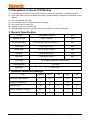
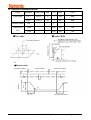
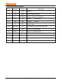
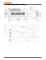
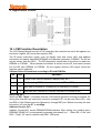
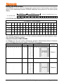
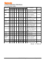
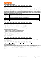
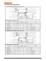
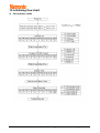
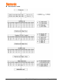
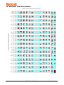
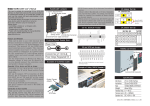
LCD Module User Manual
Customer
:
MASS PRODUCTION CODE
: TC1602D-02WA0
DRAWING NO.
: m-TC1602D-02WA0_A00
Approved By Customer:
Date:
Approved By
Checked By
Prepared By
Vatronix Holdings Limited
ADD:5F,No.10 Blg,WenGuang Industrial Zone,XiLi,Nanshan District,Shenzhen,China
TEL:0086-755-83234801 33207536 FAX:0086-755-33207539
E-mail:[email protected]
Http://www.vatronix.com
TC1602D-02WA0_A00
Page 1 of 18
Contents
1. Precautions in Use of LCD Module-----------------------------------P3
2. General Specification-------------------------------------------------------P3
3. Absolute Maximum Ratings----------------------------------------------P3
4. Electrical Characteristics--------------------------------------------------P4
5. Backlight Information-------------------------------------------------------P4
6. Optical Characteristics-----------------------------------------------------P5
7. Interface Description--------------------------------------------------------P6
8. Contour Drawing & Block Diagram--------------------------------------P7
9. Application circuit----------------------------------------------------------P8
10. LCM Function Description-----------------------------------------------P8
11. User instruction Definitions--------------------------------------------P10
11.1 Instruction table----------------------------------------------------P10
11.2 Instruction description --------------------------------------------P11
12. Timing Characteristics -------------------------------------------------P14
13. Initializing flow chart ----------------------------------------------------P15
14. Standard Character pattern--------------------------------------------P17
15.Revision records------------------------------------------------------P18
TC1602D-02WA0_A00
Page 2 of 18
1. Precautions in Use of LCD Module
(1) Avoid applying excessive shocks to the module or making any alterations or modifications to it.
(2) Don’
t make extra holes on the printed circuit board, modify its shape or change the components of LCD
Module.
(3) Don’
t disassemble the LCM.
(4) Don’
t operate it above the absolute maximum rating.
(5) Don’
t drop, bend or twist LCM.
(6) Soldering: only to the I/O terminals.
⑺ Storage: please storage in anti-static electricity container and clean environment.
2. General Specification
ITEM
STANDARD VALUE
UNIT
Number of dots
16X2 CHARs
Dots
Outline dimension
80.0(W)X36.0(H)X12.8MAX.(T)
mm
View area
65.0(W)X16.0(H)
mm
Active area
56.21(W)X11.50(H)
mm
Dot size
0.56(W)X0.66(H)
mm
Dot pitch
0.60(W)X0.70(H)
mm
LCD type
STN, Blue,Negative,Transmissive
View direction
6 o’
clock
Backlight
White LED
3. Absolute Maximum Ratings
ITEM
SYMBOL
MIN.
Operating Temperature
TOP
-20
Storage Temperature
TST
MAX.
UNIT
-
+70
℃
-30
-
+80
℃
VI
0
-
VDD
V
Supply Voltage For Logic
VDD
0
-
5.5
V
Supply Voltage For LCD
VDD-VEE
0
-
5
V
Input Voltage
TC1602D-02WA0_A00
TYP.
Page 3 of 18
4. Electrical Characteristics
ITEM
SYMBOL
Logic Voltage
VDD-VSS
Supply Voltage For LCD
VDD-VO
CONDITION
MIN.
TYP.
MAX.
UNIT
4.5
5.0
5.5
V
---
4.5
---
V
Ta=25℃
Input High Volt.
VIH
-
2.0
-
VDD
V
Input Low Volt.
VIL
-
-0.3
-
0.8
V
Output High Volt.
VOH
IoH=-0.2mA
2.4
-
VDD
V
Output Low Volt.
VOL
IoL=1.6mA
0
-
0.4
V
Supply Current
IDD
---
1.0
---
mA
-
5. Backlight Information
Absolute Maximum ratings (Ta=25℃)
Symbol
Conditions
Rating
Unit
Reverse voltage
Vr
-
5.0
V
Reverse Current
Ir
Vr=5.0V
80
uA
100
mA
240
mA
Item
Absolute maximum forward Current
Ifm
Peak forward current
Ifp
Power dissipation
Pd
340
mW
Operating Temperature Range
Toper
-30~+70
℃
Storage Temperature Range
Tst
-40~+80
℃
I msec plus 10% Duty Cycle
0
Electrical/Optical Characteristics (Ta=25 C,If=40mA)
Color
White
Wavelength
λp(nm)
---
Spectral line half
widthΔλ(nm)
Operating Voltage(V)
(±0.15V)
Forward
Current (mA)
3.1
36
---
TC1602D-02WA0_A00
Page 4 of 18
6. Optical Characteristics
ITEM
SYMBOL CONDITION
MIN
TYP
MAX
UNIT
(V)θ
CR≧2
10
-
120
deg.
(H)φ
CR≧2
-45
-
45
deg.
Contrast Ratio
CR
-
-
5
-
-
Response
T rise
-
-
200
300
ms
Time
T fall
-
-
150
200
ms
View Angle
TC1602D-02WA0_A00
Page 5 of 18
7.Interface Description
Pin No.
Symbol
Level
Description
1
VSS
0V
2
VDD
5.0V
3
VO
(Variable)
4
RS
H/L
H:Data
L :Instruction
5
RW
H/L
H:Read
L:Write
6
E
H/L
Enable signal
7~14
DB0~DB7
H/L
Data bus. DB7 is used for Busy Flag .
15
A(LED+)
+5V
Anode of LED Backlight
16
K(LED-)
0V
Ground
Power supply for Logic
Supply voltage for LCD Panel
Cathode of LED Backlight
TC1602D-02WA0_A00
Page 6 of 18
8. Contour Drawing & Block Diagram
TC1602D-02WA0_A00
Page 7 of 18
9. Application circuit
10. LCM Function Description
The LCD display Module is built in a LSI controller, the controller has two 8-bit registers, an
instruction register (IR) and a data register (DR).
The IR stores instruction codes, such as display clear and cursor shift, and address
information for display data RAM (DDRAM) and character generator (CGRAM). The IR can
only be written from the MPU. The DR temporarily stores data to be written or read from
DDRAM or CGRAM. When address information is written into the IR, then data is stored
into the DR from DDRAM or CGRAM. By the register selector (RS) signal, these two
registers can be selected.
Various Kinds of Operations according to RS and R/W Bits
RS
R/W
Operation
0
0
IR write as an internal operation (display clear, etc.)
0
1
Read busy flag (DB7) and address counter (DB0 to DB7)
1
0
Write data to DDRAM or CGRAM (DR to DDRAM or CGRAM)
1
1
Read data from DDRAM or CGRAM (DDRAM or CGRAM to DR)
Busy Flag (BF)
When the BF= "High", it indicates that the LCM internal operation is being processed. So
during this time the next instruction cannot be accepted. BF can be read, when RS = Low
and R/W = High (Read Instruction Operation), through DB7 port. Before executing the next
instruction, be sure that BF is not High.
Address Counter (AC)
Address Counter(AC) stores DDRAM/CGRAM address. After writing into (reading from)
DDRAM/CGRAM, AC is automatically increased (decreased) by 1. When RS = "Low" and
R/W = "High", AC can be read through DB0 - DB6 ports.
TC1602D-02WA0_A00
Page 8 of 18
Display Data RAM (DDRAM)
This DDRAM is used to store the display data represented in 8-bit character codes. Below
figure is the relationships between DDRAM addresses and positions on the liquid crystal
display.
High bits
AC (Hexadecimal)
AC6
AC5
Low bits
AC4
AC3
AC2
AC1
Example: DDRAM addresses 4E
AC0
1
0
0
1
1
1
0
LCM DDRAM Address(In HEX)
16 CHARs X 2 Lines Display
No.
1
2
3
4
5
6
7
8
9
10
11
12
13
14
15
16
1st Line
00
01
02
03
04
05
06
07
08
09
0A
0B
0C 0D 0E 0F
2nd Line 40
41
42
43
44
45
46
47
48
49
4A
4B
4C 4D 4E 4F
Character Generator ROM (CGROM)
The CGROM generate 5×8 dot or 5×10 dot character patterns from 8-bit character codes.
See “Standard Character pattern”.
Character Generator RAM (CGRAM)
In CGRAM, the user can rewrite character by program. Relationship between Character
Code (DDRAM) and Character Pattern (CGRAM) shown below.
Char Code(DDRAM data) CGRAM address
CGRAM data
D7 D6 D5 D4 D3 D2 D1 D0 A5 A4 A3 A2 A1 A0 P7 P6 P5 P4 P3 P2 P1
0 0 0 0 X 0 0 0 0 0 0 0 0 0 X X X 0 1 1 1
0 0 1
1 0 0 0
.
.
.
0 1 0
1 0 0 0
.
.
.
0 1 1
1 1 1 1
.
.
.
.
.
.
1 0 0
1 0 0 0
.
.
.
1 0 1
1 0 0 0
.
.
.
1 1 0
1 0 0 0
.
.
.
0 0 0 0
1 1 1
.
.
.
.
.
.
.
.
.
.
.
.
0 0 0 0 X 1 1 1 1 1 1 0 0 0 X X X 1 0 0 0
0 0 1
1 0 0 0
.
.
.
0 1 0
1 0 0 0
.
.
.
0 1 1
1 1 1 1
.
.
.
.
.
.
1 0 0
1 0 0 0
.
.
.
1 0 1
1 0 0 0
.
.
.
1 1 0
1 0 0 0
.
.
.
1 1 1
0 0 0 0
P0
0
1
1
1
1
1
1
0
Pattern
number
Pattern 1
.
.
.
1
1
1
1
1
1
1
0
Pattern 8
“X”: don’t care
TC1602D-02WA0_A00
Page 9 of 18
11. User instruction Definitions
11.1 Instruction table
Execution
time
f OSC=270KHz)
Instruction Code
Instruction
RS R/W DB7 DB6 DB5 DB4 DB3 DB2 DB1 DB0
Clear
Display
0
0
0
0
0
0
0
0
0
1
Return
Home
0
0
0
0
0
0
0
0
1
X
Entry Mode
Set
0
0
0
0
0
0
0
1
I/D
SH
Display
ON/OFF
control
0
0
0
0
0
0
1
D
C
B
Cursor or
Display Shift
0
0
0
0
0
1
X
X
Function Set
0
0
0
0
1
DL
X
X
0
0
0
1
0
0
1
0
1
BF AC6 AC5 AC4 AC3 AC2 AC1 AC0
1
0
D7
D6
D5
D4
D3
D2
D1
D0
1
1
D7
D6
D5
D4
D3
D2
D1
D0
Set CGRAM
Address
Set DDRAM
Address
Read Busy
Flag and
Address
Write Data to
RAM
Read Data
from RAM
Description
S/C R/L
N
F
AC5 AC4 AC3 AC2 AC1 AC0
AC6 AC5 AC4 AC3 AC2 AC1 AC0
Write “20H”to DDRAM
and set DDRAM address
to “00H”from AC.
Set DDRAM address to
“00H”from AC and return
cursor to its original
position if shifted. The
contents of DDRAM are
not changed.
Assign cursor moving
direction and make shift of
entire display enable.
Set display(D), cursor(C),
and blinking of cursor(B)
on/off control bit.
Set cursor moving and
display shift control bit,
and the direction, without
changing DDRAM data.
Set interface data
length(DL:4-bit/8-bit),
numbers of display line(N:
1-line/2-line), display font
type(F: 5X8 dots/ 5X11
dots)
Set CGRAM address in
address counter.
Set DDRAM address in
address counter.
Whether during internal
operation or can not be
known by reading BF. The
contents of address
counter can also be read.
Write data into internal
RAM DDRAM/CGRAM).
Read data from internal
RAM (DDRAM/CGRAM).
1.52ms
1.52ms
37µ
s
37µ
s
37µ
s
37µ
s
37µ
s
37µ
s
0µ
s
43µ
s
43µ
s
Remark:‘X’don’t care
TC1602D-02WA0_A00
Page 10 of 18
11.2 Instruction Description
1)Clear Display
RS RW DB7 DB6 DB5 DB4 DB3 DB2 DB1 DB0
0
0
0
0
0
0
0
0
0
1
Clear all the display data by writing "20H" (space code) to all DDRAM address, and set
DDRAM address to "00H" into AC (address counter). Return cursor to the original status.
Namely, bring the cursor to the left edge on first line of the display. Make entry mode
increment (I/D = "1").
2) Return Home
RS RW DB7 DB6 DB5 DB4 DB3 DB2 DB1 DB0
0
0
0
0
0
0
0
0
1
Return Home is cursor return home instruction. Set DDRAM address to "00H" into the
address counter. Return cursor to its original site and return display to its original status, if
shifted. Contents of DDRAM do not change.
3) Entry Mode Set
RS RW DB7 DB6 DB5 DB4 DB3 DB2 DB1 DB0
0
0
0
0
0
0
0
1
I/D
SH
Set the moving direction of cursor and display.
I/D: Increment / decrement of DDRAM address (cursor or blink)
When I/D = "High", cursor/blink moves to right and DDRAM address is increased by 1.
When I/D = "Low", cursor/blink moves to left and DDRAM address is decreased by 1.
* CGRAM operates the same as DDRAM, when read from or write to CGRAM.
SH: Shift of entire display
When DDRAM read (CGRAM read / write) operation or SH = "Low", shift of entire display is
not performed. If SH = "High" and DDRAM write operation, shift of entire display is
performed according to I/D value:
I/D ="1" : shift left,
I/D = "0" : shift right.
4) Display ON/OFF Control
RS RW DB7 DB6 DB5 DB4 DB3 DB2 DB1 DB0
0
0
0
0
0
0
1
D
C
B
Control display / cursor / blink ON / OFF 1 bit register.
D: Display ON / OFF control bit
When D = "High", entire display is turned on.
When D = "Low", display is turned off, but display data is remained in DDRAM.
C: Cursor ON / OFF control bit
When C = "High", cursor is turned on.
When C = "Low", Cursor is disappeared in current display, but I/D register remains its data.
B: Cursor Blink ON / OFF control bit
When B = "High", cursor blink is on, that performs alternate between all the high data and
display character at the cursor position.
When B = "Low", blink is off.
TC1602D-02WA0_A00
Page 11 of 18
5) Cursor or Display Shift
RS RW DB7 DB6 DB5 DB4 DB3 DB2 DB1 DB0
0
0
0
0
0
1
S/C R/L
Shifting of right/left cursor position or display Without Writing or reading of display data, shift
right/left cursor position or display. This instruction is used to correct or search display data.
(refer to Table 4) During 2-line mode display, cursor moves to the 2nd line after 40th digit of
1st line. Note that display shift is performed simultaneously in all the line. When displayed
data is shifted repeatedly, each line shifted individually. When display shift is performed, the
contents of address counter are not changed.
S/C R/L
Operation
0
0
Shift the cursor to the left, AC is decreased by 1.
0
1
Shift the cursor to the right, AC is increased by 1.
1
0
Shift all the display to the left, cursor moves according to the display.
1
1
Shift all the display to the right, cursor moves according to the display.
6) Function Set
RS RW DB7 DB6 DB5 DB4 DB3 DB2 DB1 DB0
0
0
0
0
1
DL
N
F
DL: Interface data length control bit
When DL = "High", it means 8-bit bus mode with MPU.
When DL = "Low", it means 4-bit bus mode with MPU.
When 4-bit bus mode, it needs to transfer 4-bit data by two times.
N: Display line number control bit
When N = "Low", it means 1-line display mode.
When N = "High", 2-line display mode is set.
F: Display font type control bit
When F = "Low", it means 5 x 8 dots format display mode
When F = "High", 5 x11 dots format display mode.
7) Set CGRAM Address
RS RW DB7 DB6 DB5 DB4 DB3 DB2 DB1 DB0
AC5 AC4 AC3 AC2 AC1 AC0
0
0
0
1
Set CGRAM address to AC. This instruction makes CGRAM data available from MPU.
8) Set DDRAM Address
RS RW DB7 DB6 DB5 DB4 DB3 DB2 DB1 DB0
0
0
1
AC6 AC5 AC4 AC3 AC2 AC1 AC0
Set DDRAM address to AC.
This instruction makes DDRAM data available from MPU. When 1-line display mode (N = 0),
DDRAM address is from "00H" to "4FH". In 2-line display mode (N = 1), DDRAM address is
the 1st line is from "00H" to "27H", and DDRAM address in the 2nd line is from "40H" to
"67H".
TC1602D-02WA0_A00
Page 12 of 18
9) Read Busy Flag & Address
RS RW DB7 DB6 DB5 DB4 DB3 DB2 DB1 DB0
1
BF AC6 AC5 AC4 AC3 AC2 AC1 AC0
0
This instruction shows whether LCM is in internal operation or not. If the resultant BF is
High, it means the internal operation is in progress and you have to wait until BF to be Low,
and then the next instruction can be performed. In this instruction you can read also the
value of address counter.
10) Write data to RAM
RS RW DB7 DB6 DB5 DB4 DB3 DB2 DB1 DB0
1
0
D7
D6
D5
D4
D3
D2
D1
D0
Write binary 8-bit data to DDRAM/CGRAM.
The selection of RAM from DDRAM, CGRAM, is set by the previous address set instruction:
DDRAM address set, CGRAM address set. RAM set instruction can also determine the AC
direction to RAM. After write operation, the address is automatically increased/decreased
by 1, according to the entry mode.
11) Read data from RAM
RS RW DB7 DB6 DB5 DB4 DB3 DB2 DB1 DB0
1
1
D7
D6
D5
D4
D3
D2
D1
D0
Read binary 8-bit data from DDRAM/CGRAM.
The selection of RAM is set by the previous address set instruction. If address set
instruction of RAM is not performed before this instruction, the data that read first is invalid,
because the direction of AC is not determined. If you read RAM data several times without
RAM address set instruction before read operation, you can get correct RAM data from the
second, but the first data would be incorrect, because there is no time margin to transfer
RAM data.
In case of DDRAM read operation, cursor shift instruction plays the same role as DDRAM
address
set instruction : it also transfer RAM data to output data register. After read operation
address counter is automatically increased/decreased by 1 according to the entry mode.
After CGRAM read operation, display shift may not be executed correctly.
* In case of RAM write operation, after this AC is increased/decreased by 1 like read
operation. In this time, AC indicates the next address position, but you can read only the
previous data by read instruction.
TC1602D-02WA0_A00
Page 13 of 18
12. Timing Characteristics
TC1602D-02WA0_A00
Page 14 of 18
13.Initializing flow chart
l
8-bit interface mode
TC1602D-02WA0_A00
Page 15 of 18
l
4-bit interface mode
TC1602D-02WA0_A00
Page 16 of 18
14. Standard Character pattern
TC1602D-02WA0_A00
Page 17 of 18
15. Revision records
Version Ref.pages
A00
All pages
Revision Items
New release
TC1602D-02WA0_A00
Date
2005.03.03
Page 18 of 18