1
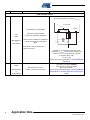
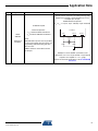
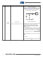
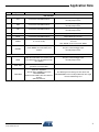
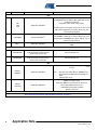
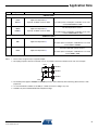
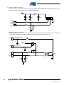
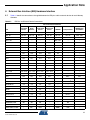
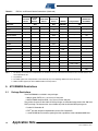
AT91RM9200 Microcontroller Schematic
Check List
1. Introduction
This application note is a schematic review check list for systems embedding the
Atmel® ARM® Thumb®-based AT91RM9200 microcontroller.
It gives requirements concerning the different pin connections that must be considered before starting any new board design and describes the minimum hardware
resources required to quickly develop an application with the AT91RM9200. This document does not consider PCB layout constraints.
AT91 ARM
Thumb
Microcontrollers
Application Note
This application note is not intended to be exhaustive. Its objective is to cover as
many configurations of use as possible.
The Check List table has a column reserved for reviewing designers to verify the line
item has been checked.
6323A–ATARM–03-Jul-07
2. Associated Documentation
Before going further into this application note, it is strongly recommended to check the latest
documents for the AT91RM9200 Microcontroller on Atmel’s Web site.
Table 2-1 gives the associated documentation needed to support full understanding of this application note.
Table 2-1.
2
Associated Documentation
Information
Document Title
User Manual
Electrical/Mechanical Characteristics
Ordering Information
Errata
AT91RM9200 Product Datasheet
Internal architecture of processor
ARM/Thumb instruction sets
Embedded in-circuit-emulator
ARM9TDMI® Technical Reference Manual
ARM920T™ Technical Reference Manual
Evaluation Kit User Guide
AT91RM9200-EK Evaluation Board User Guide
Application Note
6323A–ATARM–03-Jul-07
Application Note
3. Schematic Check List
!
Signal Name
Pin Connection
VDDCORE
1.65V to 1.95V
Decoupling/Filtering capacitors
(100 nF and 10µF)(1)(2)
VDDIOM
(3)
3.0V to 3.6V
Decoupling/Filtering capacitors
(100 nF and 10µF)(1)(2)
Description
Powers the device.
Decoupling/Filtering capacitors must be added to improve
startup stability and reduce source voltage drop.
Powers External Bus Interface I/O pads.
Decoupling/Filtering capacitors must be added to improve
startup stability and reduce source voltage drop.
Powers Peripheral I/O pads and USB transceivers.
VDDIOP(3)
3.0V to 3.6V
Decoupling/Filtering capacitors
(100 nF and 10µF)(1)(2)
VDDOSC
1.65V to 1.95V
Decoupling capacitor (100 nF)(1)(2)
Powers the Main Oscillator.
VDDPLL
1.65V to 1.95V
Decoupling capacitor (100 nF)(1)(2)
Powers the PLL cells.
GND
Ground
GND pins are common to VDDCORE, VDDIOM and
VDDIOP pins.
GND pins should be connected as shortly as possible to
the system ground plane.
GNDPLL
PLL Ground
GNDPLL pin is provided for VDDPLL pin.
GNDPLL pin should be connected as shortly as possible
to the system ground plane.
GNDOSC
Oscillator Ground
GNDOSC pin is provided for VDDOSC pin.
GNDOSC pin should be connected as shortly as possible
to the system ground plane.
Decoupling/Filtering capacitors must be added to improve
startup stability and reduce source voltage drop.
3
6323A–ATARM–03-Jul-07
!
Signal Name
Pin Connection
Description
Clock, Oscillator and PLL
Main Oscillator Internal load capacitance: 20pF
Crystal load capacitance to check (CCRYSTAL).
AT91RM9200
20 pF
GNDOSC
Crystals between 3 and 20 MHz
XIN
XOUT
Capacitors on XIN and XOUT
(crystal load capacitance dependent)
Main Oscillator
in
Normal Mode
1 Kohm resistor on XOUT only required for
crystals with frequencies lower than 8
MHz.
XIN
XOUT
1K
CL1
CL2
Note: XOUT cannot be used to drive
another clock input.
Example: for a 18.432 MHz crystal with a load
capacitance CCRYSTAL= 25 pF, external capacitors are
required: CL1= CL2 = 2x (25 pF-20 pF - Cboard)
If Cboard is about 1.5pF
CL1= CL2= 7pF.
Refer to the electrical specifications of the AT91RM9200
datasheet.
XIN
XOUT
Main Oscillator
in
Bypass Mode
4
XIN: external clock source
XOUT: can be left unconnected
1.8V square wave signal (VDDOSC)
External clock source up to 50 MHz
Duty Cycle: 40 to 60%
Refer to the electrical specifications of the AT91RM9200
datasheet for CIN and RIN values when using bypass
mode.
Application Note
6323A–ATARM–03-Jul-07
Application Note
!
Signal Name
Pin Connection
Description
Internal parasitic capacitance (including package): 6pF
Supported Crystal with a load capacitance (CCRYSTAL)
from 6pF up to 12.5 pF
Maximal External Capacitor:
CL1 = CL2 = 2 x (12.5 - 6 pF - Cboard)= 13 pF- 2xCboard.
32.768 kHz Crystal
XIN32
XOUT32
Slow Clock
Oscillator
External Capacitors:
CL1 is between XIN32 and Ground
CL2 is between XOUT32 and Ground
Note:
Wired the 32K crystal as close as possible
of the microcontroller. Do not forget to put
a guard ring and avoid having any noisy
line close to it.
XOUT cannot be used to drive another
clock input.
AT91RM9200
XIN32
XOUT32
GNDOSC
32,768 Hz
Crystal
CL1
CL2
Example: for an 32.768 kHz crystal with a load
capacitance of CCRYSTAL= 9 pF, Cboard= 1.5 pF, external
capacitors are required: CL1 = CL2 =15pF.
Refer to the electrical specifications of the AT91RM9200
datasheet.
5
6323A–ATARM–03-Jul-07
!
Signal Name
Pin Connection
Description
See the Excel spreadsheet:
“ATMEL_PLL_LFT_Filter_CALCULATOR_AT91_xxx.zip”
(available in the software files on the Atmel Web site)
allowing calculation of the best R-C1-C2 component
values for the PLL Loop Back Filter.
PLLRC
PLL
R
C2
C1
GNDPLL
PLLRCA
PLLRCB
PLL filter recommendations:
Second-order filter
Can be left unconnected if PLL not used.
The Fn parameter represents the cutoff frequency at filter
level. The higher the frequency, the better the PLL
response time. The user should choose the highest
frequency for this parameter, but be aware of the two
following constraints:
- Increasing Fn decreases the C1 and C2 values at filter
level, whereas the resulting C1, C2 values must have
values higher than the stray capacitances of the [package
+ layout].
- the Fn frequency must be at least 20 times lower than
the input frequency.
The good damping factor is the one closest to a value of
0.707.
C1 ~ 10xC2
R, C1 and C2 must be placed as close as possible to the
pins.
6
Application Note
6323A–ATARM–03-Jul-07
Application Note
!
Signal Name
Pin Connection
Description
(4)
ICE and JTAG
TCK
Connected to ICE/JTAG Interface
This pin is a Schmitt trigger input.
Internal pull-up resistor.
TMS
Connected to ICE/JTAG Interface
This pin is a Schmitt trigger input.
Internal pull-up resistor.
TDI
Connected to ICE/JTAG Interface
This pin is a Schmitt trigger input.
Internal pull-up resistor.
TDO
Connected to ICE/JTAG Interface
Output driven up to VVDDIOP
RTCK
Connected to ICE/JTAG Interface
Output driven up to VVDDIOP
NTRST
To a reset circuitry
NTRST must be driven at power up, even if JTAG port is
not used
Note: NTRST can be connected to NRST.
JTAGSEL
Must be tied to GND for normal operation
and to VDDIOP to use Boundary scan
features
This pin is a Schmitt trigger input.
Internal pull-up resistor.
Reset/Test
NRST
Must be connected to reset circuitry. The
reset delay must cover the 32Khz start up
time (900ms)
TST0, TST1
These two pins must be connected to
ground for normal operation.
PA31/BMS
Application dependent.
Must be tied to VDDIOP to boot from
Embedded ROM.
Must be tied to GND to boot from external
memory.
(EBI Chip Select 0).
This pin is a Schmitt trigger input.
Internal pull-up resistor.
The BMS signal level during reset time boots from
embedded ROM or from a 16-bit parallel Flash.This signal
must be stable during reset.
7
6323A–ATARM–03-Jul-07
!
Signal Name
Pin Connection
Description
PIO
PAx
PBx
PCx
PC6/NWAIT
PDx(5)
All PIOs are pulled-up inputs at reset except those which
are multiplexed with the Address Bus signals that must be
enabled as peripherals:
PA30 (A23), PA31 (A24) and PC3 (A25).
Application dependent.
To reduce power consumption if not used, the concerned
PIO can be configured as an output, driven at ‘0’ with
internal pull-up disabled.
(1)
A pull up is mandatory on NWAIT if this pin in not used.
If PC6/NWAIT is driven by an external device, user must
ensure that the PC6/NWAIT pin is driven high as soon as
the device is powered up.
Application dependent.
ETM features and 2nd USB HOST are available only on
PIOD.
Pull-up (100 KOhm)
Multimedia Card Interface MCI
PA28/MCCDA
Pull-up to adjust according to MultiMedia
Card specification or SD card Part1
physical layer specification
MCIA Command Line
PA8/MCCDB
Pull-up to adjust according to MultiMedia
Card specification or SD card Part1
physical layer specification
MCIB Command Line
EBI
Data bus lines D0 to D15 are pulled-up inputs to VVDDIOM
at reset.
D0-D15
(D16-D31)
A0-A22
(A23-A25)
Application dependent.
Application dependent.
Note:
Data bus lines D16 to D31 for SDRAM access.
D16 to D31 are multiplexed with the PIOC controller.
PIO input after reset.
Address Bus (A0 to A25)
A0 to A22: Address lines are driven to ‘0’ at reset.
A23 to A25 Address bus lines are:
- multiplexed with the PIOC controller.
- PIO input after reset.
SMC - SDRAM Controller - CompactFlash® Support
See “External Bus Interface (EBI) Hardware Interface” on page 11.
8
Application Note
6323A–ATARM–03-Jul-07
Application Note
!
Signal Name
Pin Connection
Description
USB Host (UHP)
No internal pull-down resistors.
HDPA
HDPB(5)
Application dependent.(6)
Typically, 15 kOhm resistor to GND.
HDMA
HDMB(5)
Application dependent.(6)
Typically, 15 kOhm resistor to GND.
To reduce power consumption, if USB Host is not used,
connect HDPA/HDPB to GND.
No internal pull-down resistors.
To reduce power consumption, if USB Host is not used,
connect HDMA/HDMB to GND.
USB Device (UDP)
No internal pull-down, no internal pull-up resistors.
DDP
Application dependent.(7)
DDM
(7)
To reduce power consumption, if USB Device is not used,
connect DDP to VDDIOP.
No internal pull-down, pull-up resistors.
Notes:
Application dependent.
To reduce power consumption, if USB Device is not used,
connect DDM to GND.
1. These values are given only as a typical example.
2. Decoupling capacitors must be connected as close as possible to the microcontroller and on each concerned pin.
100nF
VDDCORE
100nF
VDDCORE
100nF
VDDCORE
GND
3. The double power supplies VDDIOM and VDDIOP power the device differently when interfacing with memories or with
peripherals.
4. It is recommended to establish accessibility to a JTAG connector for debug in any case.
5. Available only in the 256-ball RoHS BGA compliant Package
9
6323A–ATARM–03-Jul-07
6. Example of USB Host connection:
A termination serial resistor (REXT) must be connected to HDPA/HDPB and HDMA/HDMB. A recommended resistor value is
defined in the electrical specifications of the AT91RM9200 datasheet.
5V
Type A Connector
10µF
HDMA
or
HDMB
100nF
10nF
REXT
HDPA
or
HDPB
REXT
15K
15K
7. Example of USB Device connection:
Pull-up is active by default after reset (required by the boot application). No pull-down: DM is floating when the peripheral is
not connected. The application shall monitor VBus and remove the pull-up when the host switch off.
PIOy
15 K
5V Bus Monitoring
22K
3V3
PIOx
USB Pull-up Active
1K5
1.5K
33 pF
27 R
DDM
2
1
10µF
DDP
27 R
15pF
10
3
Type B 4
Connector
15pF
Application Note
6323A–ATARM–03-Jul-07
Application Note
4. External Bus Interface (EBI) Hardware Interface
4.1
Table 4-1 details the connections to be applied between the EBI pins and the external devices for each Memory
Controller.
Table 4-1.
EBI Pins and External Device Connections
Pins of the Interfaced Device
Pin
8-bit Static
Device
Controller
2 x 8-bit
Static
Devices
16-bit Static
Device
SMC
Burst Flash
Device
SDRAM
BFC
SDRAMC
CompactFlash
NANDFlash/
SmartMedia
SMC
D0 - D7
D0 - D7
D0 - D7
D0 - D7
D0 - D7
D0 - D7
D0 - D7
AD0 - AD7
D8 - D15
–
D8 - D15
D8 - D15
D8 - D15
D8 - D15
D8 - 15
–
D16 - D31
–
–
–
–
D16 - D31
–
–
A0/NBS0
A0
–
NLB
–
DQM0
A0
–
A1/NWR2/NBS2
A1
A0
A0
A0
DQM2
A1
–
A2 - A9
A1 - A8
A1 - A8
A1 - A8
A0 - A7
A2 - A9
–
A10
A10
A9
A9
A9
A8
A10
–
A11
A11
A10
A10
A10
A9
–
–
–
–
–
–
A10
–
–
A12
A11
A11
A11
–
–
–
A13 - A14
A12 - A13
A12 - A13
A12 - A13
A11 - A12
–
–
A15
A15
A14
A14
A14
–
–
–
A16/BA0
A16
A15
A15
A15
BA0
–
–
A17/BA1
A17
A16
A16
A16
BA1
–
–
A18 - A20
A18 - A20
A17 - A19
A17 - A19
A17 - A19
–
–
–
A21
A20
A20
A20
–
–
A2 - A9
SDA10
A12
A13 - A14
A21
A22
ALE
A22
A21
A21
A21
–
A23 - A24
A22 - A23
A22 - A23
A22 - A23
–
–
–
A25
A25
A24
A24
A24
–
CFRNW(1)
–
NCS0/BFCS
CS
CS
CS
CS
–
–
–
NCS1/SDCS
CS
CS
CS
–
CS
–
–
NCS2
CS
CS
CS
–
–
–
–
NCS3/SMCS
CS
CS
CS
–
–
–
A23 - A24
REG
CLE
(3)
–
(1)
–
NCS4/CFCS
CS
CS
CS
–
–
CFCS
NCS5/CFCE1
CS
CS
CS
–
–
CE1
–
NCS6/CFCE2
CS
CS
CS
–
–
CE2
–
NRD/NOE/CFOE
OE
OE
NWR0/NWE/CFWE
NWR1/NBS1/CFIOR
WE
–
OE
–
–
OE
WE
(4)
WE
–
–
WE
WE
(4)
NUB
–
DQM1
IOR
–
11
6323A–ATARM–03-Jul-07
Table 4-1.
EBI Pins and External Device Connections (Continued)
Pins of the Interfaced Device
8-bit Static
Device
Pin
Controller
2 x 8-bit
Static
Devices
16-bit Static
Device
SMC
Burst Flash
Device
SDRAM
BFC
SDRAMC
CompactFlash
NANDFlash/
SmartMedia
SMC
NWR3/NBS3/CFIOW
–
–
–
–
DQM3
IOW
–
BFCK
–
–
–
CK
–
–
–
BFAVD
–
–
–
AVD
–
–
–
BFBAA/SMWE
–
–
–
BAA
–
–
WE
BFOE
–
–
–
OE
–
–
–
BFRDY/SMOE
–
–
–
RDY
–
–
OE
BFWE
–
–
–
WE
–
–
–
SDCK
–
–
–
–
CLK
–
–
SDCKE
–
–
–
–
CKE
–
–
RAS
–
–
–
–
RAS
–
–
CAS
–
–
–
–
CAS
–
–
SDWE
–
–
–
–
WE
–
–
NWAIT
–
–
–
–
–
WAIT
–
Pxx
(2)
–
–
–
–
–
CD1 or CD2
–
Pxx
(2)
–
–
–
–
–
–
CE
Pxx(2)
–
–
–
–
–
–
RDY
Notes:
1. Not directly connected to the CompactFlash slot. Permits the control of the bidirectional buffer between the EBI data bus and
the CompactFlash slot.
2. Any PIO line.
3. The REG signal of the CompactFlash can be driven by any of the following address bits: A24, A22 to A11.
4. NWR1 enables upper byte writes. NWR0 enables lower byte writes.
5. AT91RM9200 Restrictions
5.1
Package Restrictions
The AT91RM9200 is available in two packages:
• 208-pin green PQFP, 31.2 x 31.2 mm, 0.5 mm pitch
• 256-ball RoHS compliant BGA, 15 x 15 mm, 0.8 mm ball pitch
The product features of the 256-ball BGA package are extended compared to the 208-lead
PQFP package. The features that are available only with the 256-ball BGA package are:
• Parallel I/O Controller D
• ETM™ port with outputs multiplexed only on the PIO Controller D
• a second USB Host transceiver, opening the Hub capabilities of the embedded USB Host.
12
Application Note
6323A–ATARM–03-Jul-07
Application Note
5.2
Multiplexing Restrictions:
The AT91RM9200 features four PIO controllers:
• PIOA and PIOB
– Multiplexing I/O lines of the peripheral set
• PIOC
– Multiplexing the data bus bits 16 to 31
– Several External Bus Interface control signals.
– Using PIOC pins increases the number of general-purpose I/O lines available but
prevents 32-bit SDRAM memory access
• PIOD
– Available in the 256-ball BGA package option only, multiplexing outputs of the
peripheral set and the ETM port
6. Internal Boot Program Constraints
• PA31/BMS pin must be set to HIGH level to boot on AT91RM9200 internal boot ROM.
• PLLB must be wired:
– Associated LFT filter must be optimized for a 96 MHz running frequency with an
accuracy of ± 0.25%.
Use PLL Calculator tools (available on www.atmel.com) to estimate the filter.
• A supported crystal is mandatory between XIN and XOUT (see Table 6-1).
• Supported DataFlash devices (see Table 6-2) connected on NPCS0 or supported EEPROM
devices (see Table 6-3).
Note:
The main oscillator cannot be bypassed.
See the Boot Program section of the AT91RM9200 datasheet for more details on the boot
program.
Table 6-1.
Supported Crystals (MHz)
3.0
3.2768
3.6864
3.84
4.0
4.433619
4.9152
5.0
5.24288
6.0
6.144
6.4
6.5536
7.159090
7.3728
7.864320
8.0
9.8304
10.0
11.05920
12.0
12.288
13.56
14.31818
14.7456
16.0
17.734470
18.432
20.0
Table 6-2.
Device
Supported DataFlash Devices
Density
Page Size (bytes)
Number of Pages
AT45DB011
1 Mbit
264
512
AT45DB021
2 Mbits
264
1024
AT45DB041
4 Mbits
264
2048
AT45DB081
8 Mbits
264
4096
13
6323A–ATARM–03-Jul-07
Table 6-2.
Supported DataFlash Devices
Device
Density
Page Size (bytes)
Number of Pages
AT45DB161
16 Mbits
528
4096
AT45DB321
32 Mbits
528
8192
AT45DB642
64 Mbits
1056
8192
The DataFlash must be connected to NPCS0 of the SPI.
Table 6-3.
Supported EEPROM Devices
Device
Size
Organization
AT24C16A
16 Kbits
16 bytes page write
AT24C164
16 Kbits
16 bytes page write
AT24C32
32 Kbits
32 bytes page write
AT24C64
64 Kbits
32 bytes page write
AT24C128
128 Kbits
64 bytes page write
AT24C256
256 Kbits
64 bytes page write
AT24C512
512Kbits
128 bytes page write
Generally, serial EEPROMs have no identification code. The bootloader checks for an acknowledgment on the first read. The device address on the two-wire bus must be 0x0. The bootloader
supports the devices listed in Table 6-3
6.1
Hardware Limitations of the Internal Boot Program
The SPI and TWI drivers use several PIOs in alternate functions to communicate with devices.
Care must be taken when these PIOs are used by the application. The devices connected could
be unintentionally driven at boot time, and electrical conflicts between SPI or TWI output pins
and the connected devices may appear.
Table 6-4 contains a list of pins that are driven during the Boot Program execution. These pins
are driven during the boot sequence for a period of about 6 ms if no correct boot program is
found. The download through the TWI takes about 5 seconds for 64 Kbytes due to the TWI bit
rate (100 Kbits/s).
For the DataFlash driven by the SPCK signal at 12 MHz, the time required to download 64
Kbytes is reduced to 66 ms.
Table 6-4.
14
Pins Driven during Internal Boot Program Execution
Peripheral
Pin
PIO Line
SPI
MOSI
PA1
SPI
SPCK
PA0
SPI
NPCS0
PA3
TWI
TWD
PA25
Application Note
6323A–ATARM–03-Jul-07
Application Note
Table 6-4.
Pins Driven during Internal Boot Program Execution
TWI
TWCK
PA26
DBGU
DRXD
PA9
DBGU
DTXD
PA10
The AT91RM9200 Boot program supports serial communication via the DBGU or DFU protocol
via the USB Device Port. The USB pull-up must be active by default after reset.
7. External Boot Constraints
PA31/BMS pin must be set to LOW level.
Boot from an external 16-bit parallel Flash connected on NCS0.
All initialization (PLL,SDRAM, SMC, etc.) is user dependent.
15
6323A–ATARM–03-Jul-07
8. Revision History
Table 8-1.
Revision History
Doc. Rev
Comments
6323A
First issue
16
Change Request
Ref.
Application Note
6323A–ATARM–03-Jul-07
Headquarters
International
Atmel Corporation
2325 Orchard Parkway
San Jose, CA 95131
USA
Tel: 1(408) 441-0311
Fax: 1(408) 487-2600
Atmel Asia
Room 1219
Chinachem Golden Plaza
77 Mody Road Tsimshatsui
East Kowloon
Hong Kong
Tel: (852) 2721-9778
Fax: (852) 2722-1369
Atmel Europe
Le Krebs
8, Rue Jean-Pierre Timbaud
BP 309
78054 Saint-Quentin-enYvelines Cedex
France
Tel: (33) 1-30-60-70-00
Fax: (33) 1-30-60-71-11
Atmel Japan
9F, Tonetsu Shinkawa Bldg.
1-24-8 Shinkawa
Chuo-ku, Tokyo 104-0033
Japan
Tel: (81) 3-3523-3551
Fax: (81) 3-3523-7581
Technical Support
AT91SAM Support
Sales Contacts
www.atmel.com/contacts/
Product Contact
Web Site
www.atmel.com
www.atmel.com/AT91SAM
Literature Requests
www.atmel.com/literature
Disclaimer: The information in this document is provided in connection with Atmel products. No license, express or implied, by estoppel or otherwise, to any
intellectual property right is granted by this document or in connection with the sale of Atmel products. EXCEPT AS SET FORTH IN ATMEL’S TERMS AND CONDITIONS OF SALE LOCATED ON ATMEL’S WEB SITE, ATMEL ASSUMES NO LIABILITY WHATSOEVER AND DISCLAIMS ANY EXPRESS, IMPLIED OR STATUTORY
WARRANTY RELATING TO ITS PRODUCTS INCLUDING, BUT NOT LIMITED TO, THE IMPLIED WARRANTY OF MERCHANTABILITY, FITNESS FOR A PARTICULAR
PURPOSE, OR NON-INFRINGEMENT. IN NO EVENT SHALL ATMEL BE LIABLE FOR ANY DIRECT, INDIRECT, CONSEQUENTIAL, PUNITIVE, SPECIAL OR INCIDENTAL DAMAGES (INCLUDING, WITHOUT LIMITATION, DAMAGES FOR LOSS OF PROFITS, BUSINESS INTERRUPTION, OR LOSS OF INFORMATION) ARISING OUT OF
THE USE OR INABILITY TO USE THIS DOCUMENT, EVEN IF ATMEL HAS BEEN ADVISED OF THE POSSIBILITY OF SUCH DAMAGES. Atmel makes no
representations or warranties with respect to the accuracy or completeness of the contents of this document and reserves the right to make changes to specifications
and product descriptions at any time without notice. Atmel does not make any commitment to update the information contained herein. Unless specifically provided
otherwise, Atmel products are not suitable for, and shall not be used in, automotive applications. Atmel’s products are not intended, authorized, or warranted for use
as components in applications intended to support or sustain life.
© 2007 Atmel Corporation. All rights reserved. Atmel®, logo and combinations thereof, DataFlash ® and others are registered trademarks, SAMBA ™ and others are trademarks of Atmel Corporation or its subsidiaries. ARM ®, the ARM Powered ® logo, Thumb® and others are registered
trademarks or trademarks of ARM Limited. Other terms and product names may be the trademarks of others.
6323A–ATARM–03-Jul-07