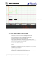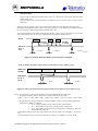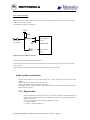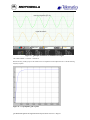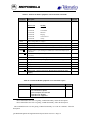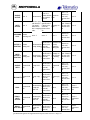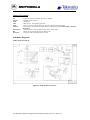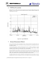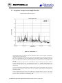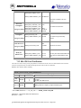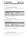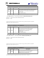
1
g18
Version 2.0
GPRS / GSM
Engine / Modem Integration
and
Application Developers
Guide
Motorola offers this information to our customer as a service to assist in the applications and engineering efforts with
our products. Motorola is basing this information only on what has been provided specifically to Motorola by our
customer. Motorola has not undertaken any independent search for additional relevant information, including any
information that may be in our customer’s possession. Furthermore, system validation of this Motorola product
within a larger electronic system remains the responsibility of our customer or our customer’s system integrator.
Manual number 98-89293L01
Contents
CHAPTER 1
THE INTEGRATOR'S TASK..........................................................17
INTRODUCTION ..............................................................................................................17
PLAN THE PRODUCT AND CREATE THE DESIGN .............................................................18
1.1.1
Develop a Usage Model ...........................................................................18
1.1.2
Develop a Message Model .......................................................................18
1.1.3
Define a Service Strategy .........................................................................19
1.1.4
Customer Problem Isolation ....................................................................19
DEVELOP AND VALIDATE THE HARDWARE ...................................................................20
1.1.5
Design the Hardware Platform................................................................20
1.1.6
Consider Power Supply Options ..............................................................20
1.1.7
Select the Source Antenna ........................................................................20
1.1.8
Set Up a Development Test Environment.................................................21
DEVELOP SUPPORTING APPLICATIONS SOFTWARE ........................................................21
TEST AND APPROVE THE PRODUCT ...............................................................................21
1.1.9
Set Up a Final Test Environment .............................................................21
1.1.10
Install and Field Test the Product............................................................21
RESOURCE ASSISTANCE ................................................................................................22
1.1.11
Integration Engineering Support .............................................................22
ENVIRONMENTAL ISSUES ..............................................................................................23
1.1.12
General Precautions ................................................................................23
1.1.13
ESD Handling Precautions ......................................................................23
CHAPTER 2
MODEL DESCRIPTION ..................................................................24
INTRODUCTION ..............................................................................................................24
D15 COMPATIBILITY WITH G18......................................................................................25
BASIC MODEL OVERVIEW .............................................................................................28
2.1.1
g18 DV Slim: ............................................................................................28
2.1.2
g18 DV Board Only – Horizontal: ...........................................................28
2.1.3
g18 DVG /slim:.........................................................................................29
CHAPTER 3
DESIGN CONSIDERATIONS .........................................................30
POWER SUPPLY CONSIDERATION. ..................................................................................30
3.1.1
Power Supply losses. ................................................................................30
3.1.2
Current consumption in g18.....................................................................31
3.1.3
How / When to make the unit to wakeup ..................................................35
AUDIO CIRCUITS CONSIDERATION..................................................................................38
3.1.4
Digital audio. ...........................................................................................38
3.1.5
Analog Audio without Hands free. ...........................................................39
3.1.6
Analog Audio – Levels..............................................................................40
3.1.7
Analog audio with hands free...................................................................44
DATA PORT CONSIDERATIONS. ......................................................................................45
g18 Modem Integration and Application Developers Guide version 2.0 Page 2
3.1.8
Data levels................................................................................................45
3.1.9
DTR line & DCD line...............................................................................47
3.1.10
Setting Baud Rate .....................................................................................47
SIM LINES CONSIDERATION. .........................................................................................48
3.1.11
SIM Card Support ....................................................................................48
ESD CONSIDERATION ....................................................................................................49
ANTENNAS ....................................................................................................................49
3.1.12
Antenna Systems.......................................................................................49
3.1.13
Antenna Safety..........................................................................................49
3.1.14
Antenna Performance...............................................................................50
3.1.15
Portable Devices ......................................................................................50
3.1.16
Fixed Devices ...........................................................................................51
3.1.17
Antenna Test Methods ..............................................................................51
MECHANICS ..................................................................................................................52
3.1.18
Fixed-Mount Usage..................................................................................52
3.1.19
Fastening units with housing ...................................................................52
3.1.20
Fastening DIN units .................................................................................52
HOW TO CONNECT 3788 HANDSET TO G18....................................................................53
GPS CONSIDERATIONS .................................................................................................53
CHAPTER 4
SOFTWARE INTERFACE ..............................................................54
MODEM COMMUNICATION MODES ...............................................................................54
VOICE COMMUNICATIONS .............................................................................................54
CONFIGURATION SET-UP AND AUDIO ROUTING IN G18 .................................................55
4.1.1
Voice connectivity ....................................................................................55
4.1.2
Data Communications..............................................................................56
4.1.3
SMS Communications ..............................................................................57
4.1.4
FAX Communications ..............................................................................57
BASIC OPERATIONS .......................................................................................................57
4.1.5
Making a voice call ..................................................................................57
4.1.6
Receiving a voice call...............................................................................58
4.1.7
Commence voice communications ...........................................................58
4.1.8
Making a CSD - data call.........................................................................58
4.1.9
Receiving a data call ................................................................................59
4.1.10
How to Enable receiving of Cell Broadcast (CB) ....................................59
4.1.11
g18 set-up in CSD mode...........................................................................59
SENDING AND RECEIVING DATA IN DIFFERENT FLOW CONTROLS...................................60
4.1.12
Flow control set to hardware Flow Control (FC)....................................60
4.1.13
Flow Control - Flow Control set to - Xon/Xoff ........................................61
4.1.14
Flow control set to ‘None’ .......................................................................62
CALL WAITING, CALL FORWARDING, AND CONFERENCE CALLS.....................................63
SENDING SMS...............................................................................................................64
4.1.15
Sending a SMS Message in PDU Mode ...................................................64
4.1.16
Sending SMS in PDU Mode - Wave Forms..............................................66
4.1.17
Sending a Fax...........................................................................................68
4.1.18
How to Establish GPRS PDP Context .....................................................69
4.1.19
How to change PIN code number ............................................................70
g18 Modem Integration and Application Developers Guide version 2.0 Page 3
4.1.20
How to write into the Fix Dialling (FD) phone book...............................70
BASIC AT COMMANDS ..................................................................................................71
ERROR CORRECTION AND COMPRESSION (ECC) COMMANDS.......................................74
FAX CLASS 1 COMMANDS .............................................................................................75
ETSI 07.07 STANDARD .................................................................................................75
V.25TER COMMANDS APPLICABLE TO GSM .................................................................79
ETSI 07.05 STANDARD (SMS) .....................................................................................81
4.1.21
Block Mode...............................................................................................81
4.1.22
Text Mode.................................................................................................82
4.1.23
PDU Mode................................................................................................83
GPRS COMMANDS ...................................................................................................84
CHAPTER 5
HARDWARE......................................................................................85
5.1
HOST INTERFACE ..............................................................................................85
5.1.1
Modem I/O Connector..............................................................................85
5.1.2
Interface Cable.........................................................................................85
ANTENNAS ....................................................................................................................85
5.1.3
GSM Antenna ...........................................................................................85
5.1.4
GPS Antenna ............................................................................................86
5.1.5
Antenna Cable Assembly..........................................................................86
DEVELOPERS KIT ..........................................................................................................87
OPTIONAL ACCESSORIES ...............................................................................................87
DEALER CONTACTS .......................................................................................................87
CHAPTER 6
TESTING ............................................................................................92
INTRODUCTION ..............................................................................................................92
TESTING STAGES ...........................................................................................................92
6.1.1
Hardware Integration ..............................................................................92
6.1.2
Enabler Functions ....................................................................................92
6.1.3
Specific Tests ............................................................................................92
6.1.4
Desense and EMI .....................................................................................93
6.1.5
Regulatory Compliance............................................................................93
6.1.6
Application Software................................................................................94
FINAL ASSEMBLY ..........................................................................................................94
6.1.7
End User Problem Resolution..................................................................94
6.1.8
OEM Service Depot Repair......................................................................95
6.1.9
Diagnostic Utility .....................................................................................95
6.1.10
Quality Assurance Testing .......................................................................95
EQUIPMENT TEST SET-UP ..............................................................................................96
6.1.11
Calibration Tools and Equipment ............................................................96
6.1.12
Set Up the Modem for Testing..................................................................96
6.1.13
Loop-back Test .........................................................................................96
ANNEX A
GLOSSARY -.........................................................................................98
ANNEX B
CUSTOMER SPECIFICATION .........................................................104
ANNEX C
USER MANUAL ..............................................................................115
g18 Modem Integration and Application Developers Guide version 2.0 Page 4
1.
BASIC FUNCTIONALITY ......................................................................115
1.1
PIN and PUK Code Entry ..........................................................................115
1.2
Feedback from the system ..........................................................................116
1.3
How to establish a Voice Call ....................................................................117
1.4
How to answer a Voice Call.......................................................................118
1.5
How to find a phonebook entry ..................................................................118
1.6
Write a phonebook entry ............................................................................119
1.7
Read a phonebook entry.............................................................................119
1.8
Phone book function...................................................................................120
1.9 How to send a SMS in PDU mode....................................................................120
1.10 How to establish GPRS PDP context............................................................121
2. AT COMMAND LISTING ..........................................................................................122
2.1
ATD, Dialling .............................................................................................122
2.2
AT+CAOC, Advice of charge.....................................................................123
2.3
AT+CCFC, Call forwarding number and conditions ................................124
2.4
AT+CCWA, Call waiting ...........................................................................125
2.5
AT+CHLD, Call related supplementary services ......................................126
2.6
AT+CLCC. List current calls .....................................................................130
2.7
AT+CLCK, Facility lock ............................................................................132
2.8
AT+CLIP, Calling line identification presentation ...................................133
2.9
AT+CLIR, Calling line identification ........................................................134
2.10 AT+CMEE, Report mobile equipment .......................................................134
2.11 AT+CMGS, Send SMS message .................................................................135
2.12 AT+CNUM, Subscriber number ................................................................135
2.13 AT+COPS, Operator selection ..................................................................136
2.14 AT+CPBS, selected phonebook memory storage.......................................138
2.15 AT+CPBW, Write phonebook entry ...........................................................140
2.16 AT+CPIN, Enter pin ..................................................................................142
2.17 AT+CREG, Network registration...............................................................143
2.18 AT+CSTA, Select type of address ..............................................................144
2.19 AT+CBST, Select bearer service type ........................................................145
2.20 AT+CGMI, Request manufacturer identification ......................................146
2.21 AT+CGMM, Request model identification ................................................146
2.22 AT+CGMR, Request revision identification ..............................................147
2.23 AT+CGSN, Request product serial number identification ........................147
2.24 AT+CHUP, Hang up call...........................................................................147
2.25 AT+CMGD, Delete SMS message .............................................................148
2.26 AT+CMGF, Message Format ....................................................................149
2.27 AT+CMGL, List messages .........................................................................149
2.28 AT+CMGR, Read messages.......................................................................150
2.29 AT+CPAS, Phone activity status................................................................150
2.30 AT+CPBR, Read phonebook entries..........................................................151
2.31 AT+CPMS, Preferred message storage .....................................................152
2.32 AT+CSCA, Service center address ............................................................153
2.33 AT+CSCS, Select TE character set ............................................................153
2.34 AT+CSMS, Select message service ............................................................154
g18 Modem Integration and Application Developers Guide version 2.0 Page 5
2.35
2.36
2.37
2.38
2.39
2.40
2.41
2.42
2.43
2.44
2.45
2.46
2.47
2.48
2.49
2.50
2.51
2.52
2.53
2.54
2.55
2.56
2.57
2.58
2.59
2.60
2.61
2.62
2.63
2.64
2.65
2.66
2.67
2.68
2.69
2.70
2.71
2.72
2.73
2.74
2.75
2.76
ANNEX D
AT+CSQ, Signal quality.............................................................................155
AT+CEER, Extended error report .............................................................155
AT+CKPD..................................................................................................156
AT+FCLASS, Select mode .........................................................................157
AT+GCAP, Request complete capabilities list ..........................................157
AT+CMOD, Call mode ..............................................................................158
AT+CRLP, Radio link protocol..................................................................158
AT+CR, Service reporting control ............................................................159
AT+CRC, Cellular result codes .................................................................160
AT+CNMI, New message indications to TE+CNMI..................................161
AT+CMEC, Mobile Equipment control mode ...........................................163
AT+CMER, Mobile Equipment event reporting ........................................164
AT+CPBF, Find phonebook entries ..........................................................165
AT+CESP , Enter SMS block mode ...........................................................166
AT+CMGW ,Write message.......................................................................167
AT+CTFR1, divert an Incoming call to the voice mail.............................167
AT+CNMA, DTE confirms previous message ...........................................167
AT+CBAND, change band.........................................................................168
AT+CBAUD, set the baud rate ..................................................................168
AT+CGPRS, GPRS coverage.....................................................................169
AT+CGPADDR, Show PDP address .........................................................169
AT+CGCLASS, GPRS MS class ................................................................169
AT+CGDCONT, define PDP context ........................................................170
AT+CGQMIN, Quality of Service Provider...............................................171
AT+CGACT, PDP context activation/deactivation request.......................171
AT+CGATT, GPRS attach/detach request.................................................172
AT+CGQREQ, define/modify/remove a requested Quality of Service Profile
173
AT+CIMI, Request international mobile subscriber identity (IMEI) ........174
AT+CRSM, Restricted SIM access.............................................................174
AT+CPOL, Preferred operator list............................................................175
AT+CIPE, ENABLE +CIP AT command..................................................176
AT+CIP, IP primitive over AT command ..................................................177
AT+CRTT, Ring Tone Selection.................................................................177
AT+CPWD, Change password ..................................................................179
Fax AT Commands .....................................................................................180
AT+MTDTR, DTR line test command......................................................180
AT+MTCTS, CTS line test command .........................................................180
AT+MCWAKE, DTE Wake line control command ...................................181
AT+CMSS, Send Message from Storage...................................................181
AT+MMGL, List of messages ....................................................................181
AT+MMGR, List of messages ....................................................................182
AT+MMGA , Change message attribute....................................................182
G18 EVALUATION BOARD ............................................................183
EV BOARD ISSUE P4 ...................................................................................................183
EV BOARD ISSUE P5 ...................................................................................................190
g18 Modem Integration and Application Developers Guide version 2.0 Page 6
ANNEX E QUICK START ........................................................................................196
1.
2.
3.
4.
5.
6.
7.
8.
9.
POWER CONNECTION ...........................................................................................196
G18 CONNECTION. ..............................................................................................196
CUSTOMER CONNECTIONS ...................................................................................196
AUDIO CONNECTION ............................................................................................196
SIM CONNECTIONS .............................................................................................196
BAND SELECTION ................................................................................................196
RS232 CONNECTION ...........................................................................................197
ANTENNA CONNECTION ......................................................................................197
DEFAULT DIP SWITCH/JUMPER SETTING ..............................................................197
ANNEX F
DESENSE.............................................................................................198
1. DESENSE DEFINED ..............................................................................................198
2. NOISE SOURCES ..................................................................................................199
3. RECEIVER SUSCEPTIBILITIES ...............................................................................199
4. MEASUREMENT TECHNIQUES ..............................................................................199
5. PACKET MODEM INTEGRATION TESTER (PMIT) .................................................200
6. PMIT DATA PRESENTATION ...............................................................................201
7. ALTERNATE MEASUREMENT METHOD ................................................................201
8. PREPARING THE DEVICE UNDER TEST .................................................................202
9. PERFORMANCE GOALS ........................................................................................202
10.
RADIO PERFORMANCE CAPABILITIES ..............................................................203
11.
DETERMINE EMISSION LEVEL GOALS .............................................................203
12.
ACCEPTANCE ANALYSIS ON A SAMPLE DATA SET ..........................................204
13.
PREDICTION OF SOURCES ................................................................................205
14.
PROBABILITY OF CHANNEL INTERFERENCE .....................................................205
15.
DESENSE SCENARIOS ......................................................................................205
16.
METHODS OF CONTROLLING EMISSIONS .........................................................206
16.1 Shielding Approach ....................................................................................206
16.2 Components of the Shield Design...............................................................206
17.
BENEFITS OF THE SHIELDING APPROACH ........................................................207
18.
ALTERNATE EMI REDUCTION METHODS ........................................................207
18.1 Clock Pulling..............................................................................................207
19.
RF NETWORK ISSUES ......................................................................................208
20.
ANTENNA ........................................................................................................208
20.1 Field Strengths from the Antenna...............................................................208
20.2 Antenna Interactions ..................................................................................209
20.3 Antenna Cable Routing ..............................................................................209
21.
DESENSE SUMMARY ........................................................................................209
ANNEX G
1.
2.
3.
4.
5.
6.
IPS OVER AT COMMANDS LIST ..................................................210
GENERAL ............................................................................................................210
ENABLE IP OVER AT SERVICES +CIPE ...............................................................210
DSC BUS IP PRIMITIVE OVER AT SERVICES +CIP ..............................................211
IP PRIMITIVES SUPPORTED BY CIP......................................................................212
REQUEST/CONFIRM PRIMITIVES ..........................................................................213
UNSOLICITED PRIMITIVES ....................................................................................213
g18 Modem Integration and Application Developers Guide version 2.0 Page 7
7.
IP PRIMITIVES CIP SPEC ......................................................................................214
7.1
Class Indicator ...........................................................................................214
7.2
Power Down...............................................................................................217
7.3
Phonebook Related Primitives ...................................................................217
7.4
Display Indicator Primitives ......................................................................219
7.5
Background ................................................................................................220
7.6
Call Restrictions.........................................................................................220
7.7
Call Status Indication.................................................................................221
7.8
Generate DTMF Signalling........................................................................223
7.9
Hook-switch Status Indicator .....................................................................225
7.10 Microphone Mute Primitives......................................................................226
7.11 SEEM Interface ..........................................................................................227
7.12 Idle SIM Card Notification.........................................................................228
7.13 SIM Card Deactivation Notification ..........................................................229
7.14 SIM Card Activation Notification ..............................................................229
7.15 SIM Card Security Notifications ................................................................229
7.16 Attached peripherals ..................................................................................233
7.17 IP_HF_AUDIO_STATUS_IND..................................................................235
7.18 IP_SET_RING_LEVEL_REQ.....................................................................236
7.19 IP_SET_RING_LEVEL_CNF.....................................................................236
7.20 IP_LOW_VOLTAGE_IND .........................................................................237
7.21 IP_GET_HF_VOLUME_REQ ...................................................................237
7.22 IP_GET_HF_VOLUME_CNF ...................................................................237
7.23 IP_LTC_ERASED_IND .............................................................................238
8. IP PRIMITIVES CIP EXAMPLES .............................................................................238
g18 Modem Integration and Application Developers Guide version 2.0 Page 8
I
Revision History
Revision
1.0
2.0
Date
7 April 01
15 Oct 01
Purpose
G18 developer guide first version
Update VII Customer Assistance
Update table2 "g18 compatibility with d15" Ch. 2
Turn On/Off timings" Ch. 3.1.2
Update "How / When to make the unit to wakeup" Ch. 3.1.3
Update audio levels Ch. 3.1.6
Update "Port Configuration" at Ch. 3.1.8
Update DTR & DCD lines - Ch 3.1.9
New Chapter "Setting Baud rate" - Ch. 3.1.10
Update "Sending Fax" Ch. 4.1.17
New Chapter "How to establish GPRS context" Ch 4.1.18
New Chapter" How to change Pin code number" Ch 4.1.19
New Chapter " How to write into the fix dialling (FD) phone book" Ch. 4.1.20
Update table 13 in " Basic AT Command list"
Update table 16 in "Advance AT command list"
Update table 23 in "ETSI 07.07 mobile equipment Control and status commands"
Update table 25 in "V.25ter commands used with GSM"
Update table 29 in "ETSI 07.05 text mode"
Update table 30 in "ETSI 07.05 PDU mode"
Update Spec. Annex B
Update Annex C. Ch. 1.1, 1.2, 1.3, 1.4, 1.8, 2.1, 2.5, 2.6, 2.7, 2.13, 2.14, 2.15, 2.16,
2.17, 2.22, 2.27, 2.37, 2.46, 2.54, 2.57, 2.58, 2.59, 2.70, 2.71, 2.72
Add in Annex E "Default Dip switch/Jumpers setting"
New Annex G "IPs over AT commands list"
g18 Modem Integration and Application Developers Guide version 2.0 Page 9
II Using This Guide
This guide presents critical research and development (R and D) issues affecting the design and
development of products incorporating the Motorola g18 900/1800/1900MHz GSM/GPRS Integrated
Wireless Modem, used in North America, Asia, and Europe.
The purpose of this document is to describe the technical details needed to integrate g18 Tri-band 900, 1800
and 1900 MHz Data Module into a host device. The g18 Data Module is the next generation that replaces
the current d15 Data Module. There are several configurations of this product that are described with in this
document that provides flexibility in full system integration needs
NOTE: A product that incorporates the modem is referred to as the Original Equipment
Manufacturer (OEM) host or simply the host.
III Purpose
Data terminal equipment (DTE) OEM teams are often pulled together quickly from other work groups. For
this reason, OEM team members often need advice about how to best sustain a concerted design and
development effort. The goal of this guide is to assist your team to successfully produce a wireless product
that integrates a Motorola g18 wireless modem.
This guide strives to bridge the gap between the various engineering and business disciplines that make up
OEM teams. Our approach is to provide a practical disclosure of useful information that can offer a common
understanding of the problems you may encounter and examples of probable solutions.
We at Motorola want to make this guide as helpful as possible. Keep us informed of your comments and
suggestions for improvements. You can reach us initially by Email : GSM [email protected]
IV Intended Audience
Our readers are intended to be data terminal equipment (DTE) OEM integration team members. Teams
historically consist of representative from the disciplines of hardware, software, and RF engineering. These
readers will probably find the entire document useful, if not enlightening. Other readers include marketing,
business, and program managers. These readers might find the first chapter, which discusses the integrator’s
task, to be sufficiently informative for their needs. The remaining chapters go into more detail.
V Disclaimer
This guide provides advice and guidelines to OEM teams. Responsibility for how the information is used
lies entirely with the OEM. Statements indicating support provided by or offered by Motorola are subject to
change at any time.
Motorola reserves the right to make any changes to this specification
g18 Modem Integration and Application Developers Guide version 2.0 Page 10
VI Reference Documents
•=
•=
•=
•=
•=
•=
•=
•=
•=
•=
•=
•=
•=
•=
•=
•=
•=
•=
Electromagnetic Compatibility: Principles and Applications by David A Weston, published by Marcel
Dekker, Inc., 270 Madison Avenue, New York, NY 10016 USA.
GSM 07.07 - prETS 300 916, Digital cellular telecommunication system (Phase 2+); AT command set
for GSM Mobile Equipment (ME), Version 5.2.0 or higher, Reference RE/SMG-040707QR1
GSM 07.05, Digital cellular telecommunication system (Phase 2+); Use of Data Terminal Equipment Data Circuit terminating; Equipment (DTE-DCE) interface for Short Message Service (SMS) and Cell
Broadcast Service (CBS), Version 5.3.0, August, 1997, Reference TS/SMG-040705QR2
GSM 03.40, Digital cellular telecommunication system (Phase 2+); Technical realization of the Short
Message Service (SMS) Point-to-Point (PP), Version 5.3.0, July 1996, Reference TS/SMG040340QR2
GSM 04.11 Digital cellular telecommunication system (Phase 2+); Point-to-Point (PP) Short Message
Service (SMS) support on mobile radio interface, Version 5.1.0, March 1996, Reference TS/SMG030411QR
GSM 03.38, Digital cellular telecommunication system (Phase 2+); Alphabets and language-specific
information, Version 5.3.0, July 1996, Reference TS/SMG-040338QR2
GSM 11.10-1, Digital cellular telecommunication system (Phase 2); Mobile Station (MS) Conformance
specification; Part 1: Conformance specification. Draft pr ETS 300 607-1, March 1998, Reference
RE/SMG-071110PR6-1
GSM Specifications are orderable from Global Engineering Documents, 15 Inverness Way East,
Englewood, Colorado 80112-5704 USA 303-792-2181 800-624-3974
ETSI Standard PCS - 11.10-1
GSM 02.30 Supplementary services.
GSM 03.90 USSD stage 2.
GSM 11.14 SIM toolkit.
ITU-T V.25ter
GSM Data Adapter for Motorola Handsets, AT command reference, Rev 2, June 9 1997.
ETSI standard SMG31.
GSM 05.02.
ETSI 07.60.
ETSI 0.7.07 Ver. 7.5.0.
g18 Modem Integration and Application Developers Guide version 2.0 Page 11
VII Customer Assistance
This page is placed as a source of contact information for any possible queries that may arise.
Have questions
Trouble getting the evaluation board set up
Technical questions
Configuration questions/problems
Technical operating problems
Need documentation
GSM data module Customer Support Center is ready to assist you on integration issues
Help desk phone number is: +972-3-5684040
Email : [email protected]
At Motorola, Total Customer Satisfaction is a top priority. If you have a question, a suggestion or a concern
about your Motorola g18 product. Motorola wants to hear from you.
Please contact the Motorola Cellular Response Center by Fax on +44 (0) 131 458 6732 or use one of the
local phone numbers in the following countries for general product inquiries.
Austria
Belgium
Denmark
Eire
Finland
France
Italy
Luxembourg
Netherlands
Canada
0800297246
0800 72 370
4348 8005
01 402 6887
0800 117036
0 803 303 302
02 696 333 16
0800 21 99
0800 022 27 43
1 800 461 4575
Norway
Portugal
Sweden
Switzerland
UK
Honk Kong
People’s Republic of China
Singapore
United States of America
22 55 10 04
21 318 0051
08 445 1210
0800 553 109
0500 55 55 55
852 25063888
86 10 68466060
65 4855 333
1 800 331 6456
Accessory items available to aid the developer.
S9002B
Developer Kit
Kit contains:
Hardware
01-85702G03
Antenna adapter cable 30-85720G01
Flex cable, 36 line ZIF 30-85717G04
Flex cable, 30 line ZIF 30-85717G01
Chip SIM card, phase 2 81-02430Z04
Antenna
Handset
HUC
BD, evaluation
85-09397T03
SCN5011A
SYN9048A
FTN8071B
Notes:
1. The part number 8102430Z04 refer to Test SIM card. The supplier is Gemplus International GmbH.
2. On the SIM card supplied with the developer's kit, if when using them the pin number is requested, it will
be “0000”
3. Manual for the handset with details of the menu structure is available from the Customer Support Center.
Accessory individual items
SCN5012A
Handset without SIM
SYN6962A
Headset
SYN4937A
Headset
SSN4018A
Speaker
SMN4097A
MIC
HFK9200A
DHFA Digi
39-03920K01
Antenna contact on EV board
8287427L01
GPRS Wizard
FTN8105A
D15 EV board Retrofit kit for g18 support - Contact salesman for details.
g18 Modem Integration and Application Developers Guide version 2.0 Page 12
If you wish to place an order, please contact your Account Manager. A list of Motorola Account Managers
is available at www.mot.com/ies/telematics/. Click onto "Products", then "Data Modules" then "Contact
Us".
VIII Regulatory Requirements
Investigate and Obtain Regulatory Approval
Most countries where the final product will be sold currently require approval from the local government
regulatory body. It is your responsibility to investigate and obtain the proper regulatory approval and
certification for each country in which the product is sold. Motorola can provide the contact names and
phone numbers of the regulatory bodies in each country.
You are required to obtain regulatory approval of products that integrate a g18 integrated wireless modem.
The specific details for achieving regulatory approval vary from country to country.
Worldwide, government regulatory agencies for communications have established standards and
requirements for products that incorporate fixed, mobile, and portable radio transmitters. To this end,
Motorola provides g18 modems as certified in specific regional markets to levels of compliance
appropriate for an integrated device. Approvals are required for two interrelated reasons: to guard public
safety and to ensure electrical non-interference
UL, CSA, and other safety approvals are not required, except that AUSTEL safety approval in Australia is
required of network operators. This means, in Australia the network operators might pass AUSTEL safety
requirements through to the device integrators.
IX
Full-Product Certification
As the integrator, you must determine what additional specific regulatory requirements are required of the
country in which your product is marketed. This means that your product must be individually certified,
even though the g18 modems are already approved. The certification process includes submittal of
prototype products and acceptable test results.
Be prepared for the certification process for your product to take from a few weeks to several months. Its
duration can be affected by safety requirements, the type of product, and the country in which you are
seeking approval.
X Country Requirements
These country requirements are provided as a general orientation to the certification processes in specific
regions and countries. You are strongly encouraged to use the services of a consultant or a full-service test
house if you have limited expertise in meeting the regulatory requirements of a specific country.
XI Countries of the European Union and EFTA
Since April 8th 2000 radio and telecommunication equipment are regulated under directive 1999/5/EC of the
European Union. This directive is referred to as the RTTED.
For equipment within its scope the RTTED supersedes the Telecommunication Terminal Equipment
directive (TTE 98/13/EC), the Electromagnetic Compatibility Directive (EMC 89/336/EC) and the Low
Voltage Directive (LVD 73/23/EC).
g18 Modem Integration and Application Developers Guide version 2.0 Page 13
The RTTED and important information about it is published by the European Commission under wed
address:
http://www.europa.eu.int/comm/enterprise/rtte/infor.htm
The requirements of the RTTED are given in article 3:
- Health and Safety in Article 3.1(a),
- EMC in Article 3.1 (b),
- Radio in Article 3.2,
- Optional requirements in article 3.3.
The harmonised standards used for the g18 to demonstrate compliance with the R&TTE directive are:
- EN60950 for Health and Safety,
- ETS 300 342 –1 for EMC in Article 3.1 (b),
- CTR 19 and 31as relevant parts of TBR 19 and TBR 31 for Radio.
- No optional requirements are applicable to GSM terminal equipment.
The implication of the RTTED is that integrators of the g18 will need to raise their own Declaration of
Conformity under the RTTED using Annex III, IV or V.
Motorola recommends integrators of the g18 to document their compliance activities in a technical
construction file under the following circumstances the Motorola test report for the g18 can be used to
demonstrate compliance with article 3.2 of the RTTED:
- The g18 must be operated at the voltages described in the technical documentation.
- The g18 must not be mechanically or electrically changed.
- Usage of connectors should follow the guidance of the technical documentation.
A Declaration of Conformity and test reports for the g18 will be available upon request from Motorola.
Requests should be made to your contact person within Motorola
Care should be taken as a product might fall under the scope of other directives or standards depending on
the type of product.
The g18 is not approved under the automotive directive (95/54/EC), as it cannot be connected directly to the
power supply or other systems of a vehicle without having additional electronic interfacing.
XII North American GSM type certification
The g18 complies with the requirements of PCS 1900 Type Certification scheme as setup by the PCS
1900 Type Certification Review Board (PTCRB) and is listed as PCS 1900 Type Certified product. This
certification will be invalidated if the following conditions are not met:
- The g18 must be operated at the voltages described in the technical documentation.
- The g18 must not be mechanically or electrically changed.
- Usage of connectors should follow the guidance of the technical documentation.
- Handsets or external card readers must be certified.
XIII United States of America
The Federal Communications Commission (FCC) requires application for certification of digital devices in
accordance with CFR Title 47, Part 2 and Part 15. This includes Electromagnetic Energy Exposure (EME)
testing. As the g18 modem is not a stand alone transceiver but is an integrated module, the g18 cannot be
tested by itself for EME certification. It is, however, your responsibility to have your completed device
tested for EME certification
g18 Modem Integration and Application Developers Guide version 2.0 Page 14
XIV Canada
This class B device also complies with all requirements of the Canadian Interference-Causing Equipment
Regulations (ICES-003).
Cet appareil numérique de la classe B respecte toutes les exigences du Règlement sur le matériel brouilleur
du Canada.
X V Regulatory Statement
The following regulatory statement for the E.E.A applies to the g18 type MG1-4F21 only:
1.
2.
3.
4.
5.
6.
7.
The g18 must be operated at the voltages described in the technical documentation.
The g18 must not be mechanically nor electrically changed. Usage of connectors should follow the
guidance of the technical documentation.
The g18 is type approved under CTR 5 ed.2 and CTR 9 ed.2. Using different external card readers or
handsets other than those approved by Motorola will invalidate the type approval and require retesting
and re-approval by the British Approval Board – Telecommunications (BABT). Such testing can only
be carried out with prior approval of Motorola. It must be noted that CTR 5 ed.2 and CTR 9 ed.2 are
expected to be repealed by October 24th. 1998, but changes approved prior to that date can be
marketed after October 24.
The g18 has been designed the meet the EMC requirements of ETS 300 342.
When integrating the g18 into a system, Motorola recommends testing the system to ETS300342-1.
The g18 meets the safety requirements of EN60950.
Systems using the g18 will be subject to mandatory EMC testing under directive 89/336/EEC and
only optional (see 3.) GSM type approval testing under directive 98/13/EEC. Other directives like the
LVD directive 73/23/EEC might also be applicable to a system using g18.
The g18 is type approved at BABT. Changes subject to type approval should be communicated to
Motorola and BABT, and are not subject for discussion with other Notified Bodies.
The above statement has been made on the basis of Motorola long experience in GSM type approvals for the
E.E.A. and reviews with BABT of the UK. Motorola recommends that integrators of the g18 consult
Motorola in the design phase to clarify any regulatory questions.
XVI g18 type certification identifications
Europe
US
Canada
PTCRB
XVI
MT3-411A21
FCC ID IHDT6AC1
CANADA 109331257A TYPE ACPA or CAN 109331257A TYPE
g18
Safety
User Operation
Do not operate your telephone when a person is within 8 inches (20 centimeters) of the antenna. A person or
object within 8 inches (20 centimeters) of the antenna could impair call quality and may cause the phone to
operate at a higher power level than necessary and expose that person to RF energy in excess of that
established by the FCC RF Exposure Guidelines.
IMPORTANT: The telephone must be installed in a manner that provides a minimum separation distance
of 20 cm or more between the antenna and persons to satisfy FCC RF exposure requirements for mobile
transmitting devices.
IMPORTANT: To comply with the FCC RF exposure limits and satisfy the categorical exclusion
requirements for mobile transmitters, the following requirements must be met
g18 Modem Integration and Application Developers Guide version 2.0 Page 15
Antenna Installation
1. A minimum separation distance of 20 cm must be maintained between the antenna and all persons.
2. The transmitter effective radiated power must be less than 3.0 Watts ERP (4.9 Watts or 36.9 dBm EIRP).
This requires that the combination of antenna gain and feed line loss does not exceed 16 dBi.
g18 Modem Integration and Application Developers Guide version 2.0 Page 16
CHAPTER 1
The Integrator's Task
This section provides background information and points out the objectives and tasks of
reaching the goal of a successful implementation.
Areas of Focus
\
Serial Port
pass
through
capability
Understanding
RF Design
Software
and
Hardware
Benefits
Enables modem diagnostics without
need to disassemble your OEM device
Provides the required network coverage.
Sets end-user performance criteria- your competitive
advantage
Reduces risk of costly re-designs
Provides reliable operation through a stateof-the-art functional Interface.
Helps ensure longer service life and fewer
field returns
Figure 1 - Integrator’s Tasks
Introduction
As an OEM integrator, you must accurately choose where and how a wireless technology will facilitate
communication for your customers. You will also have to evaluate which technical considerations will give
your product an edge over the competition.
To successfully integrate g18 wireless modems into their host platforms, you must perform the following
tasks:
•=
•=
•=
•=
Plan the product and create the design
Develop and validate the hardware
Develop supporting applications software
Test and approve the product
As you review these tasks, allow sufficient time for such required activities as the regulatory approval
process, (see Regulatory Requirements) to identify critical path activities up front.
g18 Modem Integration and Application Developers Guide version 2.0 Page 17
Plan the Product and create the Design
To plan the product and create the design, perform the following steps:
•= Develop a usage model.
•= Develop a message model.
•= Define a service strategy.
•= Investigate and obtain regulatory approval.
1.1.1 Develop a Usage Model
The usage model answers the question, “How will the end product be used (portable or mobile;
eight hours, seven days a week; and so on)?”
Perhaps the most important enabler of success is a clear determination of how the final product is
to be used. This steers the development process, because all design considerations drive toward
meeting the needs of the final user. For example, design issues related to a mobile device, such as
alternator noise and vibration, are completely different from considerations required for a fixedpoint telemetry application powered by a solar panel. Defining what is and what is not important
to the end user helps to make the critical engineering trade-off decisions that are inevitable in
every product design.
It is your responsibility to develop the usage model. Motorola is available to provide assistance
and answer questions, but is not directly involved in this phase of the project.
1.1.2 Develop a Message Model
The message model defines how many messages are sent/received and how often. To create the
message model, determine how much and how often data will be sent in each of the up link
(terminal to network) and down link (network to terminal) directions.
Answer the question, “Is there a requirement for the terminal to be on and able to receive eight
hours a day, or does the user turn the unit on only when making a query to the host system?” The
answer has a direct bearing on the battery size and capacity requirement for powering the device.
The amount of data sent and received is relevant in calculating the cost of airtime and deciding on
which type of network connection to use. In short, the message model is required source data for
making many engineering design decisions, especially in calculating such values as sleep time
versus wake time and in determining battery capacity requirements.
You are responsible for developing the message model. (For more information, see “Message
Traffic Model” on page27.) The typical approach to creating the model is to define the peak and
average network throughput requirements based on input from the user. Motorola is available to
provide current consumption figures for each of the various modes of operation (receive and
transmit, for example).
The network throughput of the host device depends on many factors in addition to the raw
throughput of the radio channel. For example, in addition to the overhead involved in forward
error correction and support for packet headers, the number of active users on the network can
directly affect network throughput.
g18 Modem Integration and Application Developers Guide version 2.0 Page 18
1.1.3 Define a Service Strategy
The service strategy determines whether the integrated modem is the cause of a user’s problem
and sets a policy for keeping the end user operational during repair. The service strategy must
consider all potential service situations and evaluate them in light of the usage model. You can
create the service strategy jointly with Motorola. Contact your Motorola OEM sales representative
for details.
To ensure that a final product can be efficiently serviced, it is recommended you design for
serviceability early in the R and D process. At a minimum, you could develop a functional service
strategy that contains a well-considered procedure for performing unit-level screening. The test
may primarily determine whether a fault lies with the modem or with the product. The test must
also screen for network problems and human error.
Motorola has an evaluation board (a standalone test fixture). The evaluation board provides a
mounting platform and electrical interface to the modem. Testing is performed much more
efficiently while the modem is being integrated within the OEM host, whether for a factory endof-line test or while at the user’s site. (See Annex E)
For your product to allow integrated testing of the modem, you may decide to provide a modem
pass-through mode.
A thoroughly developed OEM serviceability plan typically includes a needs assessment for
developing software utilities that can assist in identifying communication problems between the
product and the modem and between the modem and the RF network.
These utilities must be able to send commands to the modem, evaluate the modem responses,
perform network connectivity testing, and verify data communication with the network.
Such a software utility is essential for field service engineers and shop technicians to diagnose
problems with the product and to troubleshoot a problem to a failed assembly or mismanaged
communication link.
1.1.4 Customer Problem Isolation
When customer problems are reported from the field, you must isolate the source of the problem
remotely. You will need to determine what piece of the over all system is not functioning
correctly. The following need to be considered as source of the problem:
1.
2.
3.
Network
g18 wireless modem
Host product
Often it is a user’s misunderstanding of how to use the product. Regardless, remote
troubleshooting is essential to reducing the number of returned products and lowering service
costs, particularly if the host must be disassembled for removal of the modem.
Motorola recommends that your product application (both at the terminal and host ends)
incorporate sufficient problem diagnostic software to determine the cause of the problem
remotely. Often, the best approach is to incorporate progressively deeper loop back tests to
determine the point at which the communication link fails.
As stated elsewhere, you need to make this remote diagnostic functionality be part of your
standard software load.
g18 Modem Integration and Application Developers Guide version 2.0 Page 19
Develop and Validate the Hardware
To develop and validate the hardware, perform the following steps:
•= Design the hardware platform
•= Consider power supply options
•= Select the source antenna
•= Set up a development test environment
1.1.5 Design the Hardware Platform
Integrating a wireless modem into a hardware design requires many steps. Here again, the usage
and message models are necessary to calculate issues such as battery size, heat dissipation,
isolation from EMI, and physical mounting of the unit to ensure proper grounding. See “Design
Considerations” Chapter 3
Hardware design is your responsibility. Motorola can provide recommendations where applicable.
Motorola also provides a one-time verification of EMI-caused desense with the modem integrated
into the host. To clarify, the host device can introduce electromagnetic interference, which will
interfere with the performance of the modem. This EMI can be conducted into the modem via the
serial and power lines, or radiated into the antenna and antenna cable. It is your task to minimize
the generation of EMI by your device so that the modem’s RF performance is minimally affected.
Contact your Motorola OEM representative for details.
1.1.6 Consider Power Supply Options
Power supply requirements vary according to the usage and message models. Beyond accounting
for the current drain of the modem in its various operating modes, consider ripple and noise on the
power lines and the ability to supply sufficient instantaneous current to allow proper operation of
the transmitter. Also, ensure that your power supply can accommodate the highest power
consumption for the g18 modem that you want to integrate.
Together, these requirements define the type and size of power supply (for example, linear versus
switched) to use with the wireless modem. These issues are discussed in more detail see “design
considerations” Chapter 3
1.1.7 Select the Source Antenna
The ERP generated by the antenna peak must meet the requirements of the various network
operators: 3.16 watts ERP. Consider these network requirements when you select an antenna
system. See “Antennas” in Chapter 3.
You are responsible for selecting a suitable antenna and submitting the final product to the
network operator for certification. Motorola is available for consultation and to provide contact
information for suitable antenna vendors.
g18 Modem Integration and Application Developers Guide version 2.0 Page 20
1.1.8 Set Up a Development Test Environment
A number of development test aids are available to assist in hardware and applications
development. Motorola makes the modem hardware and an evaluation board available for
purchase; the evaluation board is a specially developed circuit board with test points and jumper
switches. The evaluation board allows for maximum flexibility in accessing and controlling
connections into and out of the modem. Motorola also provides various software utilities that can
help in performing development tests. See “Testing” in chapter 6
Supplementing the test environment supported by Motorola, the network operator sometimes
provides a live development network, one separate from the production network on which you can
develop and test your application. You must negotiate directly with the network operator for
airtime and for building and maintaining a development test environment at their facility.
Develop Supporting Applications Software
To develop supporting applications software, perform the following steps:
•= Select a communications model
•= Develop end-to-end applications software
Test and Approve the Product
To test and approve the product, perform the following steps:
•= Perform EMI and desense testing (refer to Annex G p.170)
•= Set up a final test environment
•= Install and field test the product
1.1.9 Set Up a Final Test Environment
To ensure proper assembly of the final product (antenna properly connected, serial port
operational, and so on), perform an end-to-end test that proves the final product can receive and
transmit at the required signal levels. In locations where the final assembly test is performed
within network coverage area, this test is relatively simple. But in locations where network
coverage is not available, or for products to be shipped to another country, it is necessary to test
by secondary means.
The final assembly test must verify that all connections to the modem are made
correctly. Testing on a network is not required.
1.1.10 Install and Field Test the Product
When the product is shipped to a site, it is installed or mounted in a particular location, one that
might restrict RF communications. The service question is whether the behaviour of a
dysfunctional product is caused by poor coverage or a network service provider is down. To
guarantee that the modem is located in an area of good coverage and that an end-to-end loop back
message is possible, your product needs a software application to perform the test.
Your most effective approach to field-testing is to include an installation test procedure as part of
your standard software load. Motorola can recommend specific network information that you can
obtain from the modem describing how to implement an end-to-end loop back test. See “Testing”
chapter 6.
g18 Modem Integration and Application Developers Guide version 2.0 Page 21
Resource Assistance
Developing and testing a wireless integrated product requires a well-equipped development lab and access
to resources and outside information. Table1, “Parts and Tools Requirements,” below identifies required
development and service tools. Additional topics note where the tools are available and how to get further
assistance.
1.1.11 Integration Engineering Support
Questions on this manual and the integration process can be handled by the integration
engineering teams located in Europe and North America.
Send email to:
[email protected] , with your name, phone number, company name, description of the
project and your question and an engineer will be assigned to your project. The engineer will then
contact you by phone or by email to assist you in resolving your issue.
Table 1 - Parts and Tools Requirements
Related Documentation
GSM Specifications
Refer to the Reference Documents Section
www.etsi.org
Unique Development and Service Aids
Host Evaluation Board kit
P/N S9002
This board provides interface connectors and
circuitry to allow the modem to be powered and
interfaced to a host device (PC) via a serial port and
cable.
Includes instructions, interface ribbon cable, jumpers
Mounting hardware, antenna and Antenna cable.
For evaluation board problems contact
+972-3-5684040
Modem Test Equipment
GSM Test Set
Rohde and Schwarz CMU 200 with GPRS option
Hewlett Packard 8960 with GPRS option
www.rsd.de
GPS Test Set
Welnavigate GS700 or GS1010
www.hp.com
Wireless Verification Equipment
Live Network
Where available a Live network can be used
Network operator
Traditional Shop Equipment
Power Supply
Dual Power Supply with 3-6V/2A and 12V/2A
output supplies
Commercial Items
(12V for optional Hands-free only – g18 EV board)
Oscilloscope
900Mhz, digital Storage
Commercial Item
Digital Volt meter
Fluke 77 Multimeter or equivalent
Commercial Item
g18 Modem Integration and Application Developers Guide version 2.0 Page 22
Environmental Issues
g18 Integrated Wireless Modems are designed for a combination of easy serviceability and general
raggedness. These integrated modems are designed to be housed in an OEM host product. The modem is
tested to conform to the environmental levels (for example, industrial use specifications and PC card
standards) that meet the intended applications of most integrators. If you need additional raggedness and
safety in your products, you must engineer the environmental characteristics of your host product to achieve
a special safety rating.
1.1.12 General Precautions
Follow these precautions when you work with wireless modems.
•= Minimize handling of static sensitive modules and components.
•= Wear a grounded anti-static wrist strap while handling static-sensitive components.
•= Do not bend or stress the modem in any way.
•= Reinsert connectors straight and evenly to avoid causing short and open circuits.
1.1.13 ESD Handling Precautions
Any electronics device contains components sensitive to ESD (electrostatic discharge). For
example, people experience up to 35 kV ESD, typically while walking on a carpet in low humidity
environments. In the same manner, many electronic components can be damaged by less than
1000 volts of ESD. For this reason, you must observe the following handling precautions when
servicing this equipment:
•=
•=
•=
•=
•=
•=
Always wear a conductive wrist strap.
Eliminate static generators (plastics, styrofoam, and so on) in the work area.
Remove nylon or polyester jackets, roll up long sleeves, and remove or tie back loose
hanging neckties, jewellery, and long hair.
Store and transport all static sensitive components in ESD protective containers.
Disconnect all power from the unit before ESD sensitive components are removed or
inserted, unless noted.
Use a static safeguarded workstation, which can be set up by using an anti-static kit
(Motorola part number 0180386A82). This kit includes a wrist strap, two ground cords, a
static control table mat, and a static control floor mat.
The Motorola part number for a replacement wrist strap that connects to the tablemat is
4280385A59.
•=
•=
•=
•=
When anti-static facilities are unavailable, use the following technique to minimize the
chance of damaging the equipment:
Let the static sensitive component rest on a conductive surface when you are not holding it.
When setting down or picking up the static sensitive component, make skin contact with a
conductive work surface first and maintain this contact while handling the component.
If possible, maintain relative humidity of 70-75% in development labs and service shops.
Note: G18 was tested for ESD according to EN 61000-4-2
g18 Modem Integration and Application Developers Guide version 2.0 Page 23
CHAPTER 2
Model Description
This section describes the g18 integrated wireless modem (Figure2), including accessories, physical and electrical
characteristics, features and functional capabilities, and the data-exchange network over which they communicate.
This section also provides specific performance specifications.
For model numbers and languages supported see Annex A
Figure 2 - g18 data module
Introduction
The g18 modem is supporting two modes of operation
1. A Phase II + GSM class 4 embedded module package with voice, data, fax, and short message service
(SMS) support.
2. GPRS module supporting Packed data communication in 900/1800/1900 MHz bands.
The g18 GPRS features will include full over-the-air Class B features using and handset with multi-slot
Class 1,2 and 4. Additionally, CS1-CS4 GPRS Coding Schemes will be supported (Coding Schemes are
used to manage the error rate in the transmission of data to the mobile).
If you have both RS232 and DSC bus interfacing g18, so you have the GPRS class B ability - or in other
words, you can answer a voice call, while you in GPRS mode. It's the same as if you have a handset
connected - it's also DSC bus.
The g18 is designed to support a range of subsidiary services associated with navigation, emergency
services, road tolls, security systems such as car alarm, fire alarm, etc. as well as integrated standard voice /
data/ GPRS communication. Applications where data modules can provide these benefits include
automotive Telematics, mobile computing, asset management, remote utility meter reading, street light
control, home security, vending and copy machine management, fleet management, ATM security, POS
connectivity, household appliance monitoring and control, display systems, load management and many
more. To support this flexibility, the same functionality is offered in several different configurations. GPS
capability is also provided in an additional configuration.
The modem relies on system software for basic operational instructions and on configuration parameter
values to meet modem and network interface requirements.
g18 Modem Integration and Application Developers Guide version 2.0 Page 24
The g18 is designed for use in a system environment comprising a GSM mobile radio network with one or
more radio operators per country. A corresponding infrastructure of a configuration level suitable for the
use of terminal devices with two watts transmitting power is a basic requirement.
d15 compatibility with g18
The g18 was design to be compatible with the d15 with additional functionality of GPRS.
This paragraph is summarizing the differences between g18 and d15.
Table 2 - Differences Between D15 and g18
Function
D15
g18
General
GSM Type
GSM Phase II+
GSM Phase II+ + GPRS
Data Levels
Data signals at 5V.
Data signals at 3V. See details at Ph. 3.3.1
Pin 15 in ZIF connector, Pin 10 in DIN
connector "Port-out" - Not used
Pin 15 in ZIF connector, Pin 10 in DIN connector
"wake-up line" (awake G18, Awake DTE, GPRS
coverage) see details in Ch. 4.1.2
Pin 2,3 in ZIF connector, Pin 16,15 in DIN
connector - TX_EN &NU
Pin 2,3 in ZIF connector, Pin 16,15 in DIN used for
2nd UART TXD & RXD lines.
Standard, Slim(ZIF),
Slim(ZIF),
Pin-out
Mechanical
Mechanical models
DIN-Hor, DIN-Ver, GPS
DIN-Hor, GPS
Power
Current in Sleep mode
<10mA @ DRX2
<7.5mA @ DRX2
<8mA @ DRX 9
<4mA @ DRX 9
<500mS
<700mS, See details in CH 4.1.1.1
V42 bis
Support only in SoftGsm mode
Not supported
Transparent mode
Support only in SoftGsm mode
Supported
Fax class 1 & 2
Support only in SoftGsm mode
Fax class 1 using winfax
Wake unit from Sleep
mode
Special sequence is needed in the application.
Different sequence than D15 see chapter 3.1.3
Baud rate setting
Not supported
Enabled from 300 to 57600 bps See AT+CBAUD.
On/Off pulse duration
See details in Ph 3.1.2
Data options
(Auto baud rate is available between 300 to 19200
bps).
DTR/DSR lines
DSR set ON after the DTE asserted
DTR.
There is no dependency between the two
lines.
Not Used but can be entered and returned by OK
0,1 Will be supported
ATD*99
Not Supported
Request GPRS service "D "(see Ch. 4.1.2)
ATD*100
Not Supported
Manual acceptance of a network request. (see
Ch. 4.1.2)
At$
Not Supported
Supported
AT+CPOL
Not Supported
Supported (Preferred Operator List.)
AT Commands
AT+FCLASS=8
g18 Modem Integration and Application Developers Guide version 2.0 Page 25
AT+CIMI
Not Supported
IMSI Request
AT+CIP
Not Supported
AT command for IP primitives simulation.
See Ph. 4.15
AT+CRSM
Not Supported
Supported (Restricted SIM access)
AT+CPBS
+CPBS:("FD","LD","ME","MT","SM","DD")
+CPBS:("FD","LD","ME","MT","SM","DD", “RC”,
“MC”)
ATS97 Antenna detect
Not supported
Supported
ATS99
Not supported
•=
Supported. Is not saved in profile, and
need to be re-establishing after powerup.
ATS100
Not supported
•=
Supported is not saved in profile, and
need to be re-establish after power-up.
ATS101
Not supported
Will set wakeup line forever when x=1, and
reset it when x=0. ats101? Will return
current state. These operations are
allowed only when factory bit is set. When
parameters are wrong, or factory bit is not
set, return an error.
AT+CBST
(000-002,004007,012,014,065,066,068,070,071,075),(000),(0
01)
(000-002,004-007,065,066,068,
070,071),(000),(000-003)
AT+CGSN
Not supported
Supported
AT+CPWD
Not supported
Supported
AT+CRTT
Not supported
Select ring tone - Supported
CIEV: 8, x
Not supported
New indication for GPRS coverage
AT&C2
Not Supported
Supported
AT+GMI
Not Supported
Supported
AT+GMM
Not Supported
Supported
AT+GMR
Not Supported
Supported
AT+CLCC
Supported
AT +MTDTR
Not Supported
Add "dialing" state, and non standard "released"
state. Asynchronous answers are also allowed, by
using at+clcc=1
Supported for DTR line test command.
AT +MTCTS
Not Supported
Supported for CTS line test command.
g18 Modem Integration and Application Developers Guide version 2.0 Page 26
AT +MCWAKE
Not Supported
Supported for DTE Wake line control command.
MMGL
Not Supported
Supported from SW version above E6.01.10
MMGR
Not Supported
Supported from SW version above E6.01.10
MMGA
Not Supported
Supported from SW version above E6.01.10
CMSS
Not Supported
Supported from SW version above E6.01.10
CMGL
Support list of all messages only
From SW version above E6.01.10 support list of
messages for each status according to ETSI 07.05
AT+CGDCONT
Not Supported
Supported
AT+CGQREQ
Not Supported
Supported
AT+CGQMIN
Not Supported
Supported
AT+CGATT
Not Supported
Supported
AT+CGACT
Not Supported
Supported
AT+CGCLASS
Not Supported
Supported
GPRS AT Commands
g18 Modem Integration and Application Developers Guide version 2.0 Page 27
Basic Model Overview
2.1.1 g18 DV Slim:
This configuration is the smallest packaged module, which measures, 44.28 x 88.45 x 10.4 mm.
See Figure 3.
Figure 3 - g18 DV Slim data module
2.1.2 g18 DV Board Only – Horizontal:
The horizontal Board only product provides the smallest volume with a horizontal connection.
See figure 4
Figure 4 - g18 DV Board Only –Horizontal connections
g18 Modem Integration and Application Developers Guide version 2.0 Page 28
2.1.3 g18 DVG /slim:
The DVG Slim configuration provides GPS (Global Positioning System) capability housed on the
same package as the GSM Data module. This allows developers to save on integration space
when location information is needed. (Figure 5)
Figure 5 - g18 DV GPS Data Module
g18 Modem Integration and Application Developers Guide version 2.0 Page 29
CHAPTER 3
Design Considerations
When integrating a wireless modem, internal connections and placements are critical to a successful implementation.
Specific attention must be paid to the following support mechanisms:
•= DC power
•= Audio considerations.
•= Serial interface and control
•= SIM card considerations
•= ESD considerations
•= Antenna Considerations
•= Mechanical mounting
•= Desense control (see “Desense” on Annex G)
•= How to connect a 3788 handset to g18
•= GPS Considerations.
Power supply consideration.
3.1.1 Power Supply losses.
The g18 is specified to operate from 3.0V to 6.0V on the g18 input (after the flat cable losses). In
order to be able to work in the lowest battery values it is important to verify the losses in the
power supplies lines, Flat cable and in the user PCB.
The g18 is a GSM phone that transmits in pulses of about 0.5mS every 4.6mS. The Peak current is
about 1.5A.
The VCC line will drop down in the TX periods:
Transmit
Periods
.
TX
TX
TX
VCC
Figure 6 – The VCC signal during TX periods
In order to minimise the ∆ it is recommended to use a short Flat cable as possible and to put a
1000uF capacitor (or maximum possible) in the g18 VCC input.
Note: In addition to the losses recommendation, it is recommended to have a current limit in the
power supply ( 2.5-3A) in order to avoid damages in case of short.
g18 Modem Integration and Application Developers Guide version 2.0 Page 30
3.1.2 Current consumption in g18
In order to design the power supply correctly you need to take in account the current consumption
of the g18 in the different modes.
Table 3 – g18 Current consumption
Mode
Current consumption
g18 with no accessory when no call is in
process (Sleep Mode)
<4mA @ DRX9.
g18 with no accessory but TS is ON
< 50mA.
g18 during searching time
<180mA typical average 80mA.
g18 with DSC bus accessory (like Handset)
when no call is in process
Typical 45 mA.
g18 during a call in maximum power level
<1.8A Peak, Average 300mA @5V.
g18 during a call in GSM power level #10 (for
Example)
<0.7A Peak, Average 175mA @ 5V.
< 7.5mA @ DRX2.
Note: DRX2/9 is the rate that the base station, interrogate the mobile
station. The network operator sets this parameter.
3.1.2.1.
Turn On/Off the unit
The g18 is powered from a single power supply in the range of 3.0 to 6.0 Vdc.
The unit will not power up automatically by connecting the power and there are two
ways to turn the unit ON.
3.1.2.2.
Turn ON/OFF the unit using the ON/OFF pin.
The ON/OFF pin (pin # 14 at the ZIF connector & pin # 18 at the DIN connector) is
used as a toggle input to turn ON and OFF the unit. Any drop to ground in this pin
will change the status.
To verify that the unit is ON or OFF you have to check the DSC_EN line, If it is high
the unit is ON if it is low the unit is OFF.
The timing for this process is the follow:
g18 Modem Integration and Application Developers Guide version 2.0 Page 31
T1 minimum = 12ms
T2 minimum = 630ms
T3 typical = 850ms
T4 typical = 240ms
T3+T4 max =1300ms
T5 typical = 1725ms
Figure 7: Turn On the unit using the ON/OFF pin
T2 min = 630ms (T1 min = 12ms)
T3 min = 1550ms
T4 min = 630ms
T5 = 620ms
T6 = 800ms
T7 = 240ms
T8 = 5400ms
T9 = 4840ms
Figure 8: Turn On and Off the unit using the ON/OFF pin
3.1.2.3.
Turn ON the unit using the TS pin.
The main used of the TS line is for units connected to a mobile device in which the
current consumption is not the main concern.
The TS line is used to turn ON the unit. This line can’t turn OFF the unit.
When this line is rise up it will turn ON the unit.
This line is used for example to turn ON the unit when power is connected to the unit.
(Like Ignition line in a car kit).
Note - TS line should be return to low in order to be able to work in sleep mode.
g18 Modem Integration and Application Developers Guide version 2.0 Page 32
T1=600ms (on is sent after the
power was supplied for a long
time 600ms)
T2=12ms (The TS signal is
sampled on the rising edge,
therefore it size does not matter)
T3= 820ms
T4= 25ms
T5= 250ms
Figure 9: Turn ON the unit using the TS line
The following pictures show the behaviour of the RS232 lines during the turning on of
the G18 (Low level on RS232 indicates active state).
T1 max = 3.5 sec
T2 max = 5.5 sec
T1
T2
Figure10: DTR/DSR during Ton
The CTS becomes active before the DSC_EN becomes active.
g18 Modem Integration and Application Developers Guide version 2.0 Page 33
T1 max = 1.7 sec
T1
Figure11: RTS/CTS during Ton
The DCD and RI are inactive during the on/off process.
Figure12: DCD/RI during Ton
g18 Modem Integration and Application Developers Guide version 2.0 Page 34
T1
Figure13: TXD/RXD during Ton
3.1.3 How / When to make the unit to wakeup
If the g18 has no accessories, g18 is able to go to sleep mode (current save mode).
In Sleep mode the radio is switched to minimum activity. The clock is removed from the RF
section and it reduced from 13MHz to 32KHz in the Logic section.
The unit is sensing the activity by going out of this mode in a periodic sequence.
In any case of an incoming call the unit will go out of Sleep mode.
Going to sleep mode will not terminate a GPRS section and will not deactivate a context.
During sleep mode period the RS232 is not responding to any command from the DTE device
(UART is disabled and no respond will be received via the RXD line). In order to wake up the
unit, the host needs to communicate with the g18 as follow:
Two options will be available to wake the g18.
Option 1:
The sleep mode will work as follow:
At the beginning of you work activate the sleep mode by sending ATS24=n (n=1,2,3,4 seconds).
(To disable sleep mode send ATS24=0)
Then the scenario will be the follow:
The g18 will drop the CTS any time that the unit is in sleep.
When TXD is present the g18 will not go to sleep mode, After the end of the TXD (TXD buffer
empty) the g18 will wait n seconds (like set in ATS24=n) and go to sleep.
g18 Modem Integration and Application Developers Guide version 2.0 Page 35
T1 max = 1.7 sec
ATS24=n
awake
g18 sleep periods
awake
sleep
active
CTS
sleep
active
Inactive
inactive
DTE TXD
End timer n
Start timer
n
Reset timer
Start timer
n
n
Figure 14: Sleep mode timing
NOTE:
1. ATS24 factory default value is "0" this value is saved in the EEprom . To change the default value
you should save the new value to the EEprom. After recycling the power the value of S24 will be
the value saved in the EEprom. The value of ATS24 can be changed also without saved in the
EEprom but will be loosed after power recycling.
2. TS line should be low in order to be able to go to sleep mode.
3. DTE should look for active CTS before sending data (HW flow control).
4. DTE’s UART should not send any character to g18, if CTS is inactive, otherwise that character
might be lost. If the DTE’s processor handles the flow control, and not its UART, and there is a
gap between checking the CTS state and sending the start bit, g18 might set CTS inactive during
this gap, and character send to g18 might be lost.
Option 2:
At the beginning of you work activate the sleep mode by sending ATS24=n (n=1,2,3,4 seconds).
Use the wake up line to wake the G18 any time that you like to send data.
The wake up line (pin # 15 at the FC 36 pin or pin # 10 at the DIN 28 pin) will be used for this
purpose.
Any time that the DTE will want to send data he will pull this line to low, wait 30 ms
(wake time required for the g18) and than can start to send data.
The wake up line should be remained low all the period of sending data, At this time g18 will not
go to sleep.
Wakeup line
DTE TXD
30ms
Fig.15
Wake the g18 when DTE want to send data.
g18 Modem Integration and Application Developers Guide version 2.0 Page 36
Wake up the DTE:
The g18 is able to indicate the DTE that data is present or when the unit went out and came back from a
GPRS coverage area.
This will be done using the bi-directional line - Wakeup line (pin # 15 at the FC 36 pin or pin # 10 at the
DIN 28 pin)
When g18 wants to send data to DTE, g18 will activate the wakeup line to interrupt DTE, followed by data
transmission (assuming RTS is active). After 2*y ms from activation (t = pulse duration), g18 will deactivate that
line. The value of y is determined by ATS99=t (default value is 30).
G18 toggles wakeup line once, before sending the first character to DTE, when previous character was sent more
than T seconds before that. The value of T is determined by an ATS100=T (default value is 1).
Rx Data
More than
T = ATS100
Less than
ATS100
More than
T = ATS100
Wake up line
Pin 15 or
Pin 10
t = 2*ATS99
t = 2*ATS99
t = 2*ATS99
Figure 16: Wake the DTE when Data is present using the wakeup line
- Wake up the DTE when unit is going from state of non-GPRS coverage to GPRS coverage.
GPRS service
coverage
no coverage
coverage
no coverage
coverage
Min 10 sec.
Wake up line
Pin 15 or
Pin 10
t = ATS99
t = ATS99
Figure 17: Wake up the DTE when unit is going from state of non-GPRS coverage to GPRS coverage
Note: 1. The g18 will give a wakeup pulse for data sent to DTE in GPRS mode and in CSD mode.
2. The g18 will generate a wake up pulse whenever asynchronous data is sent to DTE.
(+CIEV, +CLCC, +CCWA, +CMT, +CMTI, +CBM, +CDS, +CDEV, +CLIP, +CR, +CREG, +CIP, 2 / RING
…)
3. The g18 will give a wakeup pulse whenever a change in GPRS coverage occurs, depends on dynamically
setting of AT+CWAKE=N command:
•= N = 0: Changes in GPRS coverage will not generate a wakeup pulse.
•= N = 1: When GPRS coverage is lost, g18 will generate a wakeup pulse.
•= N = 2: When GPRS coverage achieved, g18 will generate a wakeup pulse. This is the
default value after power-up.
4. S99 responds with error if the value is greater than 2,147,483,647. Value of 0 is changed to 1, No error on
that.
5. S100 responds with error if value is grater than 32,767. Value of 0 is changed to 1, No error on that.
g18 Modem Integration and Application Developers Guide version 2.0 Page 37
Less than
Wake up line architecture:
The wake up line is a bi-directional line. It is used to turn on the G18 as described in Option 2 (input to G18) and to
wake the DTE (output from G18).
The configuration of the line is the follow:
2.75V
100K
wake up line
Wake up DTE output
user connector.
G18 Processor
Wake up G18 input
Figure18: Wake up internal connections
The user need to put attention to the following points:
1. When the wake up line is used to wake the G18 (wake up line is pulled down) no wake up indication to the DTE
will be available.
2. When DTE is going to sleep mode the DTE should not load the wake up line (3 state).
Audio circuits consideration.
The g18 is able to make a voice call as well as Data calls. In voice calls the audio can be routed in a few
channels:
Digital audio channel - Audio is sent via the DSC bus.
Analog audio channel - Drive externally to audio devices.
Analog audio channel in Hands free mode - g18 send the audio out with the Echo cancelling ON in the DSP,
External drivers is required.
3.1.4 Digital audio.
In case of digital audio channel a DSC drives is in used. The consideration that should be taken in
this case is to be aware of the present of the hook switch. The hook switch will distinguish if the
handset is In/Out of use.
There are two DSC bus accessories for audio defined for the g18:
1. External Handset.
2. DHFA - Car Kit for Hands Free.
g18 Modem Integration and Application Developers Guide version 2.0 Page 38
3.1.5 Analog Audio without Hands free.
The g18 will drive the audio out/in in order to allow a voice call. In order to connect a Headset it
is needed to amplify the speaker and microphone channels,
An example for these drivers can be seen in Annex C EV board.
Other point to be taken in consideration is the Buzz noise existing in GSM phones due to the
transmission rate (217Hz). In order to minimise this noise the g18 have a separate ground for the
analog circuits.
Customer side
G18
Analog
Circuits
Analog
Ground
Digital Ground
Digital Ground
PS
Logic
Circuits
Figure 19 – Ground connections
The main problem causing the Buzz is drops in the Ground line because the peak current during
TX mode. In order to minimize the Buzz the following acts should be done:
−=
Use short Flat cable.
−=
Connect the analog ground from the g18 to all the analog circuits in the customer application
without connecting them to the power supply ground.
−=
All the capacitors to ground in the audio circuits should be connected to the analog ground.
−=
Any reference voltage that may be used should have the external capacitor connected to the
analog ground.
−=
The maximal audio In/Out levels from/To the g18 can be seen below.
−=
Connect Digital ground to the Antenna ground. (this can help also if there is sensitivity
desense due to digital signals from the used board).
−=
Connect the Digital ground of the g18 with the Digital ground of the Application.
−=
Verify that any of the Analog lines is not referenced to the Digital ground.
g18 Modem Integration and Application Developers Guide version 2.0 Page 39
3.1.6 Analog Audio – Levels
Audio Uplink (MIC)
The maximum signal level that the g18 can receive in the Audio In pin, before the signal will be saturated is:
Figure 20 – g18 Input maximum level
The maximum level that the G18 can accept before the signal at the network becomes distorted is about 500mvP-P.
The following picture shows this maximum signal:
g18 Modem Integration and Application Developers Guide version 2.0 Page 40
Figure 21 – g18 Input maximum level and BS detected signal
The CODEC 0dbm0 = 375mvrms = 1058mvP-P
Between the EX_AUDIO_IN pin to the CODEC there is an amplifier with an amplification of 3.3 and the following
frequency response:
Figure 22 – Gcap amplifier gain response
g18 Modem Integration and Application Developers Guide version 2.0 Page 41
Therefore the odbm0 of the uplink path is 375/3.3 = 113.63 mV RMS
The headroom is 20*LOG (500/(1058/3.3))= +3.86 dbm0
Audio Downlink (Speaker)
The 0dbm0 is 548mV RMS.
Max output is 2.6V p-p.
The maximum signal from the network before distortions occur was measured to be
1180mvRMS.
Therefore the headroom is 20*LOG (1180/548)= 6.66 dbm0
The following graph shows the frequency response of the analogue section:
Figure 23 – g18 analog audio frequency response (Audio Out pin)
g18 Modem Integration and Application Developers Guide version 2.0 Page 42
Voice
A 500mv RMS sin signal with a frequency of 1khz was sent from a base station to the G18.
The following amplitudes were measured on the audio out pin of the G18:
Handset volume
0
1
2
3
4
5
6
7
Amplitude (mV RMS)
27
37
51
69
100
137
196
277
Table 4 – g18 RX audio levels
Different levels were sent from the network and the signal was measured at the audio out.
The input is presented both in RMS and in dbm0. The output is at level 7.
dBm0
3.14
0
-5
-10
-15.5 ( Phone: -4.7dBPa)
-16
-17
-20 (Dispatch: -94dBSP)
-25
-30
mV RMS
1111.9
774.6
435.6
244.9
130
122.8
109.4
77.5
43.6
24.5
G18 Out (mV RMS)
580
420
237
135
70
68
61
43
24
17
Table 5 – g18 RX audio levels Vs. different signals in the BS
Tones
The OK key was pressed and the tones were measured on the audio out pin of the G18.
The same amplitude was measured during a call, and off call. All the measurements are with ATS96=0
Handset volume
0
1
2
3
4
4
5
6
7
Amplitude (mV P-P)
43
75
107
150
215
215
295
420
583
g18 Modem Integration and Application Developers Guide version 2.0 Page 43
Table 6 – g18 RX audio levels with ATS96=1
With the ATS96=1 command the amplitude was 1043 mV P-P
3.1.7 Analog audio with hands free
The audio In/Out from the g18 for analog Hands free is the same as for non-Hands free. All the
consideration from Paragraph 3.2.2 is applicable for this mode too.
The additional consideration in this case is to switch the g18 DSP to Echo cancelling mode.
In order to switch to hands free mode use the RS232 port by sending a switch command at the
start up.
ATS96=1 Echo canceller is activate. (Hands free)
ATS96=0 Echo canceller is disabled. (Headset - Default)
But during an active call the echo canceller can be activate but not disabled.
The block diagram for the required drivers are shown below, But detailed example of drivers
design you can see the Evaluation board design, Annex C
G18
SPKR
12V
MIC
A1
Audio out
Hands Free
Selection
Headset
Audio In
A2
Hands Free
Selection
VCC
REF
VCC
Vref
(for Audio amp)
Analog GND
Hands Free
Selection via
ATS96 command.
Figure 24 – EV audio block diagram
The requirements from the external drivers and audio devices are the follow:
Microphone impedance:
S/N ratio
Gain from headset to g18 (A2)
Frequency response
(including microphone)
g18 input impedance
TX Distortion
Speakerphone Load
S/N
Gain from g18 to Headset (A1)
Frequency response
(including SPKR)
g18 output impedance
Typical 700Ω
Minimum 35dB
45 – 49 dB
-11 to +1 dB 300 to 3400Hz.
10KΩ
Maximum 5%.
25 to 39 ohm
Minimum 35dB
-13 to –9 dB
-10 to +1 dB 300 to 3400Hz.
<1KΩ
g18 Modem Integration and Application Developers Guide version 2.0 Page 44
Distortion
Maximum 5%.
Data port considerations.
3.1.8 Data levels.
The g18 is a DCE device operating in 0 to 3V logic. An MC74LCX244 buffer buffers all the
In/Out signals.
DTR, DSR, RTS, CTS, DCD lines are "1" (active) in 0V and "0" (inactive) in 3V.
RXD, TXD lines are "1" in 0V and "0" in 3V.
The signal thresholds are:
Vih
Vil
Voh
Vol
2.0 V min, 5.5 V max
0.8 V max
2.5 V min @100 uA
0.2 V max @ 100 uA
Port configuration:
1 start bit
1 stop bit
8 data bits
No parity
Default Baud rate 9600bps with auto baud detect activated.
Specific baud rate can be set using AT+CBAUD=<Baud>
When a DTE is connected to the g18 (DCE device)
TXD
TXD
4
3
DTR
4
RTS
7
2
RXD
DCD
1
6
DTR
DTR
8
RTS
RTS
5
9
RI
Host Device DTE
using standard DB9
RXD
7
DCD
9
CTS
CTS
DSR
6
RXD
DCD
CTS
8
TXD
10
DSR
11
RI
G18
processor
DSR
RI
G18 is a DCE device
User connector36 pin ZIF
figure 25 – DTE connection to g18 (user connector 36 pin ZIF)
g18 Modem Integration and Application Developers Guide version 2.0 Page 45
25
TXD
TXD
DTR
7
DTR
DTR
RTS
28
RTS
RTS
TXD
3
4
7
26
RXD
RXD
DCD
14
DCD
DCD
CTS
27
CTS
CTS
RXD
2
1
8
DSR
21
DSR
6
RI
13
RI
9
Host Device DTE
using standard DB9
G18
processor
DSR
RI
G18 is a DCE device
User connector 28 pin DIN
Figure 26- DTE connection to g18 (user connector 28 pin DIN)
When a DCE is connected to the g18 (DCE device)
TXD
TXD
RXD
4
DSR
6
DTR
DTR
CTS
8
RTS
RTS
RXD
RXD
TXD
5
DCD
7
DCD
DCD
RTS
9
CTS
CTS
DTR
10
DSR
RI
11
RI
G18
processor
DSR
RI
Host is a DCE device
G18 is a DCE device
User connector36 pin ZIF
Figure 27- DCE connection to g18 (user connector 36 pin ZIF)
g18 Modem Integration and Application Developers Guide version 2.0 Page 46
RXD
DSR
25
TXD
TXD
7
DTR
DTR
28
RTS
RTS
CTS
26
RXD
RXD
DCD
14
DCD
DCD
RTS
27
CTS
CTS
TXD
DTR
21
DSR
RI
13
RI
G18
processor
DSR
RI
Host is a DCE device
G18 is a DCE device
User connector28 pin DIN
Figure 28 - DCE connection to g18 (user connector 28 pin DIN)
Note: When G18 is in sleep mode period the RS232 output lines are keeping the last stage.
There are no level changes due to the sleep stage of the unit.
3.1.9 DTR line & DCD line.
The DTR line must to be active (0V) in order to recognize the DTE by the g18.
If the DTR is not used by the application connect this line to ground (DTR Active).
The DCD line will indicate the follow:
In CSD
In GPRS mode
Indicate Carrier Detect Low during the call high in idle.
Indicate PDP context status - Active low, Inactive high
DCD will be activated only when PDP context is achieved.
DCD will be de-activated when PDP context is off.
When g18 is used in PC the DCD will be off when PDP context is achieved due to the PC dialler.
Note:
DTR indicates that DTE is ready; DSR indicates that DCE is ready. There are no connections
between the two.
3.1.10 Setting Baud Rate
Power up default baud rate is 9600, with enable auto baud rate detection feature. Baud rate can be
switched to 300, 600, 1200, 2400, 4800, 9600, 19200, 38400, 57600 using AT+CBAUD = <baud>.
g18 Modem Integration and Application Developers Guide version 2.0 Page 47
<baud> values are 0-8, 9 or 300, 600, 1200, 2400, 4800, 9600, 19200, 38400, 57600. Values 0-8
represents 300 to 57600. Value 9 represents auto baud rate detection. For example, AT+CBAUD=8
is equivalent to AT+CBAUD=57600. Using AT+CBAUD=<baud> with <baud> value other than 9,
will disable auto baud rate detection feature.
After power up, g18 UART is programmed to 9600, with automatic baud rate detection. To switch to
57600 BPS use AT+CBAUD=57600. g18 will replay with “OK<CR><LF>”. After flushing these
characters out of the UART, g18 will re-program the UART to the new baud rate.
To verify this process, DTE’s UART should switch to the new baud rate after receiving
“OK<CR><LF>”, and send AT+CBAUD? To get the new baud rate.
The answer “OK<CR><LF>” does not depend of ATVx setting (verbal or numeric response).
G18 supports auto baud rate detection for low baud rates 300 - 19200. To switch to that mode,
AT+CBAUD=9 command should be sent to g18. g18 will process this command as described
above, except that it will program UART to 9600 with auto baud rate detection. After getting the
“OK<CR><LF>” DTE can program its UART to baud rate in range 300 -19200, and verify the new
setup using AT+CBAUD?.
SIM lines consideration.
3.1.11 SIM Card Support
The g18 module has a built-in SIM card reader within the module itself. The SIM card is inserted
into the slot provided on the side of the sheet plastic cover. When inserted to the correct depth the
card should be flush with the cover. To extract the card, insert a non-conductive tuning tool into
the slot on the top of the unit at the back end of the card, and then push the card out of the slot so
that it can be removed by hand.
For some installations, this built-in slot will not be accessible, so an external card reader is needed.
If a digital handset is going to be used, the card reader can be part of the handset and is connected
to the modem via the DSC interface. Other installations require that the SIM card slot is installed
into the OEM device and circuitry is installed to connect the card reader to the g18.
The SIM card interface contains six lines plus 2 lines for presence detect, which are lines 1 and 2
as shown in figure 20.
2
5
8
4
7
1
3
6
Pin
1
2
3
4
5
6
7
8
Figure 29 – The SIM card interface
The g18 is supporting 3 types of SIM connection:
Internal SIM - Internal socket in the g18 - Support 3/5V cards.
g18 Modem Integration and Application Developers Guide version 2.0 Page 48
Description
Gnd
SIM_PD
SIM_CLK
.*SIM_RST
VSIM1
SIM_I_O
SIM_-5V
Gnd
External SIM - The SIM lines are routed in parallel to the SIM socket and to the user connector.
The user can connect the SIM externally.
IMPORTANT !!
In case of externally connection the customer concern should be for Full Type Approval that may
require submission for testing in case that the SIM lines will be longer than 10cm. Support 3/5V
cards.
Remote SIM - This is a standard connection. The SIM is connected to an external SIM socket
connected to the radio via the DSC bus. Two accessories exist - M3788 handset and external SIM
card reader. Support 5V card only.
Note: Be aware that for GPRS your SIM card should support this service.
ESD consideration
In general the ESD can be protected up to 8KV by using ceramic capacitors of 0.1uF or higher.
For all the static lines - power, SIM PD, SIM VCC, ... the capacitor will protect against ESD. The
protection was done inside the g18, but it is recommended to add protection in the user PCB, especially
if the flat cable is long.
For lines with high rate of signals it is recommended to use Transguard with low capacitance. There are
Transguard of 3pF or less.
It is recommended to ground the antenna ground contact and the power supply ground contact in order
to prevent ESD to go inside the g18 or user equipment.
Antennas
The antenna must be mounted like any other cellular or land mobile radio antenna. The best position for the
antenna is usually the center of the vehicle roof, which provides a good fairly symmetric ground plane on
metal cars. For vehicles that are fabricated of non-metallic material such as fibreglass, mount the antenna
where it won’t be obstructed by items such as mirrors.
3.1.12 Antenna Systems
Use this information to assist you in selecting the appropriate antenna to incorporate into your
product package. For specific detailed information, Motorola recommends that you use the
expertise of an antenna design engineer to solve individual application concerns.
3.1.13 Antenna Safety
The following statement from the American National Standards Institute (ANSI) specifies the
safety criteria that integrators must use when designing the antenna for a product integrating the
g18modem.
“The design of the integrated product must be such that the location used and other particulars of
the antenna comply with the then current American National Standards Institute (ANSI)
Guidelines concerning Radio frequency Energy Exposure and with any other nationally
recognized radio frequency standards that may be applicable thereto. “
g18 Modem Integration and Application Developers Guide version 2.0 Page 49
3.1.13.1. User Operation
Do not operate your telephone when a person is within 8 inches (20 centimetres) of
the antenna. A person or object within 8 inches (20 centimetres) of the antenna could
impair call quality and may cause the phone to operate at a higher power level than
necessary and expose that person to RF energy in excess of that established by the
FCC RF Exposure Guidelines.
CAUTION ! The telephone must be installed in a manner that provides a minimum
separation distance of 20 cm or more between the antenna and persons
to satisfy FCC RF exposure requirements for mobile transmitting
devices
NOTE:
To comply with the FCC RF exposure limits and satisfy the
categorical exclusion requirements for mobile transmitters, the
following requirements must be met:
A minimum separation distance of 20 cm must be maintained
between the antenna and all persons.
The transmitter effective radiated power must be less than 3.0
Watts ERP (4.9 Watts or 36.9 dBm EIRP). This requires that the
combination of antenna gain and feed line loss does not exceed 16
dBi.
3.1.14 Antenna Performance
The network operator usually sets antenna network requirements.
3.1.15 Portable Devices
In the environment where portable devices are in use, many variables exist that can affect the
transmission path. In this case, it is preferable to use a vertically-polarized, omni directional
antenna.
Antennas for portable devices include the following designs:
3.1.15.1.
Internal antenna (invisible or pull-up)
This is the most difficult antenna design scenario. Despite greater physical constraints,
an internal antenna must still provide a gain sufficient to meet network specifications.
Metal cased products cannot have internal antennae as the metal acts as a shield
around the antenna and prevents RF signals from reaching the antenna. I.E. A metal
case acts like a Faraday cage. The antenna should be positioned so that it is vertically
oriented when the device is carried normally. This will ensure that the best antenna
performance is available most of the time.
Cable routing from the modem to the antenna needs to avoid RF-sensitive circuits and
high-level, high-speed clock circuits. Consider these items:
•= The location of the antenna to avoid RFI to a computing device
•= Good shielding to the display and other RF-sensitive components
•= The most efficient method of cable routing
Otherwise, antenna gain can be offset by cable loss. A typical coaxial cable is very
thin, such as RG178B used in portable devices, and cable loss can be as high as 0.5 dB
per foot. Some coaxial cable manufacturers market relatively thin double-braid
coaxial cables. These cables show much better isolation than single-braid cables,
typically by 30 to 40 dB. These double-braid cables reduce radiation and RF pick-up
when routed inside a portable device.
g18 Modem Integration and Application Developers Guide version 2.0 Page 50
3.1.15.2. External antenna, removable and directly connected to the
device
You can design a portable device that can use an off-the-shelf, plug-in antenna, such
as a 1/4 wave monopole or 1/2 wave dipole antenna. Typical gain of these omni
directional antennas is 0 dBi and 2.14 dBi, respectively. Like the internal antenna,
these antennae should be oriented vertically when the device is normally carried to
ensure the best antenna performance.
Cabling demands the same consideration as an internal antenna application. In a
typical laptop application, the antenna must be placed as far as possible from the
display to avoid deflection. This usually causes a deep null in radiation patterns.
3.1.15.3. External, remote antenna
For remote antenna application use the same design approach as internal designs,
including the RF cable routing of the external connector. You can choose an off-theoff the shelf mobile antenna of omni directional 1/2 wave length. The antenna has
2.14 dBi of gain. Higher gain than that might not be appropriate for portable
applications.
A double-braid coaxial cable such as RG223 from the device to the antenna is
recommended if the cable length is more than a few feet. The difference in cable loss
between low-cost RG58 cable and the more expensive RG223 cable is approximately
4.5 dB per 100 feet. If the cable must be routed through noisy EMI/RFI environments,
a double-braid cable such as RG223 can reduce radiation and pick-up by 30 to 40 dB.
3.1.16 Fixed Devices
Fixed data device applications use the same design recommendations as a portable device with a
remote antenna.
As for the RF connector of an external antenna, whether it is a plug-in type or a remote type, the
most economical and practical choice is a TNC threaded connector. TNC has a good frequency
response to 7 GHz, and leakage is low. A mini UHF threaded connector provides adequate
performance and is an economical choice. If the size of the TNC and mini UHF connectors
becomes critical, consider an SMA threaded connector or an SMB snap fit connector. (The SMB
connector does not accept RG58 or RG223 cables).
3.1.17 Antenna Test Methods
Whether portable or fixed, the device antenna is the critical link to the network. A poor
performing antenna reduces the coverage of the device within the network footprint. The antenna
performance must meet the impedance and match the criteria of the modem (see the modem
specification), and have the appropriate amount of gain to meet the network ERP requirements.
Two tests must be performed on the antenna to ensure that it meets requirements. For both tests
the antenna must be integrated in its final form. That is, the antenna must be mounted on a
representative housing that includes all metal objects forming the ground plane or counterpoise.
Antenna testing requires an experienced operator and an anechoic chamber, a GTEM cell, or
approved open field site. Your Motorola OEM support representative can provide advice on this
type of testing.
g18 Modem Integration and Application Developers Guide version 2.0 Page 51
Mechanics
Mounting the g18
3.1.18 Fixed-Mount Usage
Fixed-mount usage eliminates most of the mechanical constraints of handheld designs, although
the requirements still apply. Fixed-mount units are sometimes AC-line powered and require
filtering to eliminate the 60 Hz noise that can impair modem operation.
Proper mounting of the modem requires secure fastening of it within the host housing.
To ensure ease of access for installation and troubleshooting, locate the modem within the product
in such a way that serial I/O and antenna connections are readily accessible.
Quick access to the modem allows it to be efficiently removed, probed, and functionally tested.
3.1.19 Fastening units with housing
Mount the modem to the rigid OEM product housing, using four #2-56 UNC 2A machine screws
torqued to 2 in.-lbs. Position the screws as shown in Figures 5 and 6.
3.1.20 Fastening DIN units
Secure the DIN board to the host device using three M1.8 screws.
CAUTION ! Do not mount a g18 integrated wireless modem in PC Card Type III rails.
Forcing the modem into a PC Card header can damage the connector pins in
the header and leave the modem loose and poorly grounded.
Figure 30 - Mounting the modem (front view)
Figure 31 - Mounting the modem (rear view)
g18 Modem Integration and Application Developers Guide version 2.0 Page 52
How to connect 3788 Handset to g18.
In order to connect the handset (3788) to the g18 there is a need of the following connections in the user
board.
You can see below the circuits used in the g18 Evaluation board for this purpose as an example.
To G18 User Connector
Handset Connector
In the EV board PCB
RJ-45
DSC_EN Uplink DownLink
1
P ch
2
(10.5- 15V) 12V
3
4.7K
DownLink
4
Uplink
5
6
On/Off
7
8
4.7K
2.2uF
4.7K
DSC_EN
N ch
RJ45
PCB TOP View
Mechanical
hols
7
8
5
6
3
4
1
2
TAB
Figure 32– Handset Connections / HW required
GPS Considerations
The g18 DV with GPS model includes internally a M12 GPS receiver from Motorola.
The GPS receiver is powered internally from the g18 with 3Vdc.
All the other lines of the GPS were routed to the user connector (ZIF 36 pin).
The GPS lines in the g18 user connector 36 pin ZIF socket are as follows:
Table 7 – The GPS lines in the g18 (user connector 36 pin ZIF socket)
g18 User Connector Pin #
Function
2
GPS RXD receive data in 3V logic.
3
GPS TXD transmit data in 3V logic.
34
Antenna voltage input 3 or 5 Vdc. (active antennas)
35
RTCM input - 3V logic.
36
1pps output in 3V logic.
The GPS receiver is a stand-alone unit in the g18.
More details about the M12 module can be viewed on the web at
http://www.synergy-gps.com/M12_Oncore.html
g18 Modem Integration and Application Developers Guide version 2.0 Page 53
CHAPTER 4
Software Interface
The operating functions of the g18 modem are implemented in the base unit in which the g18 is integrated. The g18 is
a GSM900/1800/1900 Phase II+ device with GPRS capability.
The corresponding functions are implemented conforming V.25ter, GSM07.07, and GSM07.05. Note that the
standards bodies regularly update these standards and so it cannot be promised that the commands supported by the
g18 exactly conform to the latest versions of that specification. Some commands listed in these standards do not apply
in the GSM environment.
AT+C commands conforming to GSM07.07 and GSM07.05 and a number of manufacturers-specific AT commands
are available via the serial interface of the g18 for the implementation of the functionality.
Command input is via the operating functions of the base unit. The base unit translates the operating functions into AT
commands and the g18 executes the requested action. Note: you should wait to OK before sending new AT command.
The modem guidelines V.25ter are applicable in regards to the time sequence of interference commands. In
accordance with this guideline, commands start with the string AT and end with a carriage return (<CR> or 0x0D).
Commands are acknowledged with OK or ERROR. A command currently being processed will be interrupted by
each subsequent incoming character, so the next command must not be sent until the acknowledgement has been
received that command has been processed. Otherwise the current command will be cancelled.
Modem Communication Modes
The g18 modem supports the following communications modes:
Voice Communications
Analog Audio - Audio communications via a standard analog headset such as the headset used with the
StarTAC cellular phone. In this case the controls for answering calls, dialling, and hanging up are provided
by the AT command set interface. This mode would be used if the modem were being integrated into a
handheld terminal that will support voice communications.
Digital Audio - Digital audio is provided by the Motorola Proprietary DSC interface. This is used when an
external handset such as would be used in an automotive installation is used. In this case, the call controls
are provided on the handset. DSC handsets that support this interface are manufactured by and available
from Motorola. The AT command set can also be used to control calls. The DSC interface is a Motorola
proprietary feature that requires licensing from Motorola. Please contact your Motorola representative for
more information.
g18 Modem Integration and Application Developers Guide version 2.0 Page 54
Configuration Set-up and Audio Routing in g18
4.1.1 Voice connectivity
The g18 is an OEM Data & Voice module.
The voice connectivity can be done in two main channels – Analog voice, Digital voice.
The Audio route for the different devices is descried in the following table:
1. HF Refer to External Speaker & Microphone connected.
2. DHFA refers to External Car kit.
Correct set-up is in bold letters.
Table 8– Voice connectivity
Configuration Setup
Audio Route to…
Off hook handset
Handset.
(overrides all other conditions)
On hook handset, or absence of handset:
−=
HF + HF was selected by ATS96 command
−=
HF external Speaker with Echo cancelling
−=
HF + HF was not selected by ATS96 command
−=
−=
DHFA
HF External Speaker, W/O Echo
cancelling
−=
Headset + HF was selected by ATS96 command
−=
DHFA Speaker
−=
Headset + HF was not selected by AT command
−=
Headset with Echo Cancelling
−=
Headset W/O Echo Cancelling
Table 9 – Regular (HS) and HF mode using RS232
Characteristics
Echo Cancelling (EC)
Sidetone
Regular Mode (Handset)
HF mode
-
+
Disable
Enable
+
Mute
Echo Suppression (ES)
•=
•=
•=
•=
+
-
Enable
Disable
Full Duplex
Half Duplex
Side-tone - When side-tones are enabled, an attenuated (reduced) version of the microphone
audio input is routed to the selected speaker. This is so that the people speaking will hear
themselves talking. This also creates a slight echo because the speaker sound then gets picked
up again by the mic and again output to the speaker, etc. Echo suppress is designed to take
care of this echo.
Echo Suppress - Cancel a little of the output sound picked up by the input device (suppress
the echo). It is designed to be used where there will be little to no echo (e.g. in a handset)
rather that where there will be much echo (e.g. in a hands-free device).
Echo Cancel - Suppress a lot of the output sound picked up by the input device (cancel all
echo).
Noise Suppress - An audio control that improves audio quality in all modes.
If the application is using DSC bus the HF selection can be done via new IP.
g18 Modem Integration and Application Developers Guide version 2.0 Page 55
Table 10 - Regular (HS) and HF mode using DSC bus
Characteristics
Regular Mode (Handset)
Echo Cancelling (EC)
HF mode
-
+
Disable
Enable
Side-tone
+
-
Echo Suppression (ES)
+
-
Enable
Disable
-
+
Mute
DSC Mic
Mute
To activate the hands free mode, see the following table:
Table 11 – HF mode selection using AT command
Command
Description
Notes
ATS96 = 1
Hands free mode ON
+
Enable
ATS96 = 0
Hands free mode OFF
Mute
Default
Hands free mode OFF
After setting the HF, it is kept in
the flex even after power cycling
the g18.
4.1.2 Data Communications
There are two modes to use the Data port:
•=
GPRS - This mode is for Package Data communication.
This mode is starting from command mode and after an initialisation of a PDP context the
data sent from the DTE will be over PPP.
An available tool to do the PDP connectivity is a GPRS wizard (for PC applications).
This is a very effective tool to transfer data in a high rate and only when data is available
without any need to dial again.
•=
CSD - Circuit Switch Data - RS232 full flow control- this is the default setting for the g18.
In this mode, we can transfer data and SMS and Fax class 1 using a full flow control (HW
flow control), Xon/Xoff or non-flow control.
The main difference from the GPRS is the need to dial to the desired number any time that
data need to be transferred.
Note: g18 does not support CSD non transparent with speed less than 4800
g18 Modem Integration and Application Developers Guide version 2.0 Page 56
Table 12 – The supported features by using CSD / GPRS
CSD
Supporting
Flow Control
Flow Control:
HW
Xon/Xoff
None
Data type
Transparent/Non transparent
SMS
SMS PDU mode.
SMS Block Mode.
Fax
Class 1
GPRS
Supporting
Flow Control
Flow Control:
HW
Xon/Xoff
None
Data type
Data over PPP
Multi slot
Class 1,2 &4, Support 1 uplink and 1,2 or 3 downlinks
Coding schemes
CS1, CS2, CS3, CS4
4.1.3 SMS Communications
Block Mode — This is a binary SMS presentation. There is a need of application SMS build for
this mode.
Text Mode — This mode is not supported by the g18.
PDU Mode — This is the recommended mode for SMS communications. Note that the PDU
packet has a complex structure, so careful examination of GSM 04.11 and GSM 03.40 is required.
4.1.4 FAX Communications
Class 1 — This is the basic set of FAX commands that is supported by all types of fax machines.
To support fax with g18 used WinFax in your PC.
Class 2 — This mode is not supported by g18.
Basic Operations
4.1.5 Making a voice call
AT+CPIN=”nnnn”
Enter PIN number which enables the SIM Card. (4-8 digits)
ATDnnnnnn;
OR
AT*Dnnnnn
ATD><index>;
ATD>”name”
ATDS=n; (n=0 to 3)
OR
OR
OR
OR
Initiates the voice call to the remote phone Commence voice
communications
The phonebook storage should be selected first at+cpbs=”sm”
Phone number corresponding to the name entered
Phone number from register #1 after setting at&z1=035658452
Phone number from register #0 after setting at&z1=035658452;
g18 Modem Integration and Application Developers Guide version 2.0 Page 57
ATDS=n (n=0 to 3)
ATD><mem><index>;
ATH
OR
Phone number from SIM card #101 for example ATD>SM101
Hangs up on voice call
Note: In Multi-party call, ATH does not end the last call, only
AT+CHLD=1 does.
4.1.6 Receiving a voice call
AT+CPIN=”nnnn”
Enter PIN number that enables the SIM Card (4 -8 digits)
AT+CRC=1
Enable cellular result codes extended format. Remote
phone dials g18 voice number
+CRING:VOICE
If AT+CRC=1 , VOICE indicates an incoming voice call.
or
+RING
if AT+CRC=0 then +RING will indicate incoming call.
Note: To get the type of the call use CMER command.
ATA
Answer call
4.1.7 Commence voice communications
ATH
Hang-up call ends
or
Note: In Multi-party call, ATH does not end the last call,
only AT+CHLD=1 does.
AT+CHUP
Behaviour if remote phone hangs up first: The modem will stay online, (AT+CPAS returns +CPAS:004)
for approximately 60 seconds, at which point it will time out and the call will be cleared (AT+CPAS
returns +CPAS: 000). At any time during this period, the modem can execute an ATH.
4.1.8 Making a CSD - data call
ATDnnnnnnn
Dial remote modem
CONNECT xxxx
Indicates connection made
+++
Escape to command mode
ATO
Return to online mode
Proceed with data communications
+++
Escape to command mode
ATH or AT+CHUP
Hang up connection
g18 Modem Integration and Application Developers Guide version 2.0 Page 58
4.1.9 Receiving a data call
Remote modem dials g18 data number.
AT+CRC=1
Enable cellular result codes extended format. Remote
phone dials g18 voice number
+CRING: REL ASYNC
If AT+CRC=1 , DATA indicates an incoming data call.
or
+RING
if AT+CRC=0 then +RING will indicate incoming call.
Note: To get the type of the call use CMER command.
ATA
Answer manually; ATS0=1 will enable automatic answer
after 1 ring
+++
Escape from online mode
ATH or AT+CHUP
Hang up call.
Note: In Multi-party call, ATH does not end the last call,
only AT+CHLD=1 does.
Behaviour if remote phone hangs up first: The modem will stay online (+CPAS:004) for approximately 60
seconds, at which point it will time out and the call will be cleared (+CPAS: 000). At any time during this
period, the modem can execute an ATH.
4.1.10 How to Enable receiving of Cell Broadcast (CB)
Send AT+CKPD=”M>>S>>>>>S<SCC”
For receiving the CB message on the TE you should use the AT+CNMI command, for example:
AT+CNMI=0,2,2,0,0
4.1.11 g18 set-up in CSD mode
g18 set to work in CSD Mode
When a data call is received the RI signal goes active low for one second and then inactive high
for four seconds repeatedly.
Figure 33 – RI waveform
After a data carrier has been detected by the g18, he sets the DCD signal active low.
Note: g18 does not support CSD non transparent with speed less than 4800
g18 Modem Integration and Application Developers Guide version 2.0 Page 59
Figure 34 – g18 Receiving a data call
Sending and Receiving data in different flow controls
4.1.12 Flow control set to hardware Flow Control (FC)
4.1.12.1.
Sending Data
When data is being sent by the g18, the only dynamic signals through the data transfer are TXD
and CTS. The DTE device should keep DTR ON.
TXD is used in order to transmit the data from the terminal to the g18, and CTS is used in order
to control the data flow. When data is being transferred too rapidly to the modem, in a rate greater
then its transfer rate, and its buffers become full, the modem sets CTS inactive high, until he
accomplishes the transfer.
When the modem is ready to accept more data, it sets the CTS signal active low again.
Figure 35 – g18 sending data HW flow control
g18 Modem Integration and Application Developers Guide version 2.0 Page 60
4.1.12.2. Receiving Data
When data is being received by the g18, the only dynamic signal during the data transfer is RXD,
on which the data is being sent to the terminal. The DTE device should keep DTR ON and RTS
can be used to alert the G18 that DTE buffer is full.
.
Figure 36– g18 receiving data HW flow control
4.1.13 Flow Control - Flow Control set to - Xon/Xoff
First, the g18 should be configured to Xon / Xoff flow control, by:
AT&K4
To return to HW flow control use - AT&K3
4.1.13.1.
Sending Data
When a data is being sent in Xon/Xoff flow control, the data is transferred on the TXD line. The
DTE device should keep DTR ON.
When the modem receives data in a high rate, its buffers may get full, and the transmission cannot
be done in this rate. Then, it sends a Xoff signal to the terminal on the RXD line.
When the modem sends the data in the buffer and its ready to receive more data, it sends the Xon
signal on the RXD line.
Figure 37 – Sending data Xon/Xoff
g18 Modem Integration and Application Developers Guide version 2.0 Page 61
4.1.13.2. Receiving Data
When data is being received in Xon/Xoff flow control, the data is being transferred from the g18
to the terminal on the RXD line. The DTE device should keep DTR ON.
Figure 38 – g18 receiving data Xon/Xoff
NOTE: In the picture above, the Zmodem transfer protocol was used, with crash recovery
setup. When an error is encountered, the terminal sends acknowledge to the
sending side, asking it to send that block again.
4.1.14 Flow control set to ‘None’
First, the g18 should be configured to Xon / Xoff by:
AT&K0
To return to HW flow control use - AT&K3
4.1.14.1.
Sending Data
When data is being sent in this mode, it is sent on the TXD line, and there is no flow control. The
DTE device should keep DTR ON.
When the modem cannot keep up with the transmission of data from the terminal, an error
happens.
Figure 39–g18 sending data in ‘none’ FC
g18 Modem Integration and Application Developers Guide version 2.0 Page 62
4.1.14.2. Receiving Data
Data is being received on the RXD line, which is the only dynamic line, in this receiving mode.
The DTE device should keep DTR ON.
Figure 40 – g18 receiving data in ‘none’ FC
Call waiting, call forwarding, and conference calls
Note: These operations are network dependent. Some networks do not support these operations.
Some behave unexpectedly, such as roaming or call dropout.
g18 Modem Integration and Application Developers Guide version 2.0 Page 63
Sending SMS
4.1.15 Sending a SMS Message in PDU Mode
AT+CPIN=”nnnn”
Enter PIN, which enables SIM card. (4 - 8 digits)
AT+CSMS=0
Select message service response; response will be
+CSMS:001,001,001
AT+CPMS=”SM”
Select preferred message storage; response will be
similar to +CPMS:001,0015,001,015 depending on
your SIM card.
AT+CMGS=<length of TPDU><cr>
<SCA><TPDU><ctrl-Z>
<SCA>: Service Center Address, refer to GSM 04.11
<TPDU>: Transport Protocol Data Unit, refer to GSM
03.40
Example:
AT+CMGS=19
>07914483056100F511000B914410927856F40000000541E1905804<0x1A>
Will return +CMGS:000 after sending “ABCDE” to phone number 44-012-987-654 via the SMS
center at 44-385-016-005. Note this is an example only; this particular SMS center is an UK
number.
The following ASCII string is the ASCII representation of the hexadecimal values that will be
transmitted as a binary string. So, ‘F’’4’ below means that the hex values 0xF and 0x4 will be
transmitted over the air. CMGS=19 is the length of the TPDU in octets, see below. Note that the
message is terminated with a Control-Z character (0x1A)
AT+CMGS=19
>07914483056100F511000B914410927856F40000000541E190F804<CTRL-Z>
07 = LENGTH OF SCA element including the TON/NPI
91 = TON/NPI,TON=9=Type of number, NPI=1=Numbering Plan Identifier
4483056100F5 SCA =SERVICE CENTER ADDRESS
I.E. the real phone number for the SCA is 44-385-016-005
•=
Explanation of coding of phone numbers. One hex digit for each phone number digit will be
used. Each pair of hex digits is considered an octet (8 bit binary number). Then the two hex
digits are reversed in order to form a semi-octet. So, The phone digits 3,8 will become 0x3,
0x8, then 0x38, and then reversed to become 0x83. The ASCII characters ‘8’ and ‘3’, ie the
string ‘83’ are then inserted into the full ASCII string above. Since there are an odd number
of digits, the last digit 5, is placed in the lower nibble of the last octet and then it top nibble is
filled with 1’s. So ‘5’ becomes 0x5, then 0x05, then 0xf5, and then ‘f5’, the last two
characters in the Service Center address.
Refer to ETSI 04.11 for more detail.
Looking at the rest of the message after the SCA we find the Transport Protocol Data Unit
(TPDU), which contains the destination device address (phone number), and the user data or
message. There are 38 characters, which represent 19 octets, which is the length of the TPDU.
11000B914410927856F40000000541E190F804 = TPDU
11 = 8 bits MTI,RD,VPF,SRR,UDHI,RP,MMS,SRI
00 = MR Message Reference
0B914410927856F4 = DA Transport Destination Address.
0B = Number of digits (11) in phone number
91=TON/NPI (as above)
4410927856F4 = Destination phone number 44-012-987-654.
g18 Modem Integration and Application Developers Guide version 2.0 Page 64
Note that the destination phone number is converted to an ASCII string in the same manner
as the SCA.
After the phone number is the user data control information and the user data.
0000000541e190f804
00 = PID Protocol ID
00 = DCS Data Coding Scheme
00 = VP Validity Period
05 = UDL User Data Length
41E190F804 = The user data ‘ABCDE’.
The user data is encoded as a GSM characters.
•=
Description of encoding the user data. The GSM character set is a method of encoding 7 bit
ASCII characters into 8 bit numbers. GSM only supports 128 characters with ASCII values
0x00 to 0x7f. Since these only need 7 bits to define them, and the SMS message is
transmitted as a series of 8-bit values, GSM uses a method of packing the series of 7 bit
values into 8 bit octets. To explain:
ABCDE is encoded as 41E190F804 as follows.
A
B
C
D
E
In ASCII hexadecimal is:
0x41 0x42 0x43 0x44 0x45
In 8 bit binary is:
01000001 01000010 01000011 01000100 01000101
We truncate off the most significant bit, resulting in a series of seven bit values. The process is to
pack the now unused most significant bit(s) with enough least significant bits from the following
value to fill it up to eight bits.
‘A’
0x41
‘B’
0x42
‘C’
0x43
‘D’
0x44
‘E’
0x45
1000001
1000010
1000011
1000100
1000101
01000001
11100001
10010000
01011000
00000100
This results in the string of eight-bit hexadecimal numbers 0x41, 0xE1, 0x90, 0x58, 0x04. By
continuing this process a string of 160 ASCII characters can be stored as a string of 140 bytes
(octets).
The Service Center Address is described in ETSI GSM 04.11.
The Transport Protocol Data Unit is described in ETS GSM 03.40.
Note:
Sending and Receiving SMS messages interfere with each other, when the time in between is
too short, or when both operations are taking place at the same time.
g18 Modem Integration and Application Developers Guide version 2.0 Page 65
4.1.16 Sending SMS in PDU Mode - Wave Forms
4.1.16.1.
Sending SMS in CSD mode
When sending SMS in PDU mode, after executing the at+cmgs=n command, the DCD line goes
active low, and the data is transferred on the TXD line.
After executing the <Ctrl+Z> command, the DCD line goes inactive high again, and the message
is being sent by the phone.
Figure 41 – Sending SMS
4.1.16.2. Receiving a SMS message
AT+CPIN="nnnn"
Enter PIN which enables SIM card. (4 -8 digits)
AT+CSMS=0
Select message service
AT+CPMS="SM"
Select preferred message storage
Allow buffer unsolicited result codes in the TA and
indication of memory location is routed to TE
will be displayed (001 message location)
AT+CNMI=0,1
+CMTI: "SM",001
To display incoming messages:
AT+CMGL=4
Lists all stored messages
AT+CMGR=1
Reads message at location 001
+CMGR: 000,,102
038021430402802100006990502100000064D22792580
49940D321F21A946A4153F45B4E0735CBF379F85C0
64DCB727B7A5C0651CB73BA0B44459741D17A7AB
C0609E5EFBB1B647CE341CA7A1B3E073DED65398
88A2E8398617D1E447C9F5DA0986C46ABD96EB81C
4C01
OK
g18 Modem Integration and Application Developers Guide version 2.0 Page 66
Once the message has been received, the next step is to decode it into something readable. This
particular message is generated by a Rohde and Schwarz CMD55 GSM Test station. Looking at
the first line of data we see the information about the service center, followed by the TPDU.
038021430402802100006990502100000064D2279258049940D321F21A946A4
03 = Length of service center address
80 = Type of number = unknown, number plan identifier = unknown
2143 = Service center address = 1234
04 = MTI = SMS-DELIVER, MMS = no more messages,
SRI = no status report UDHI = no UD header, RP =
reply path not set
02 = OA length
80 =TON = unknown, NPI = unknown
21 = OA = 12
00 = PID =Protocol ID
00 = DCS = Data Coding Scheme
69905021000000=SCTS Service Center Time Stamp
= 5th Sept. 1996 12:00:00 GMT
64=UDL=User Data Length=100 octets
Now looking at the user data.
D2279258049940D321F21A946A4153F45B4E0735CBF379F85C064DCB727B7A5C0651CB73
BA0B44459741D17A7ABC0609E5EFBB1B647CE341CA7A1B3E073DED6539888A2E839861
7D1E447C9F5DA0986C46ABD96EB81C4C01
This is a string of GSM characters, and must translate back to ASCII. The process is the reverse of
the coding process described above. This converts them back from a series of octets to a series of
7 bit ASCII numbers.
Looking at the first 6 octets:
D2 27 92 58 04 99
0xD2
0x27
0x92
0x58
0x04
0x99
11010010 00100111 10010010 01011000 00000100 10011001
1010010
0x52
1001111
0x4F
1001000
0x48
1000100
0x44
1000101
0x45
0100000
0x20
‘R’
‘O’
‘H’
‘D’
‘E’
‘ ‘
This decoding process continues for the entire user data string. Translating the entire string comes
up with ROHDE & SCHWARZ THE QUICK BROWN FOX JUMPED OVER THE LAZY
DOG.
g18 Modem Integration and Application Developers Guide version 2.0 Page 67
4.1.16.3. Sending and receiving binary data via SMS
Your specific application may require sending binary data, instead of an ASCII text message. In
this case, you could simply insert your raw data as the user data, instead of using the GSM
character coding process. This will limit you to 140 octets of data. As long as your application
controls the encoding and decoding of the SMS PDU’s at either end of the solution, you can use
the 140 octets of user data as you see fit.
4.1.16.4. Receiving SMS in CSD mode - Wave Forms
When receiving SMS the message is stored on the SIM card.
The following picture shows a reading command being sent on the TXD line, and the message
transferred from the SIM card to the terminal.
Figure 42 – Receiving SMS
4.1.17 Sending a Fax
Installing modem driver:
Control Panel-> Modems-> add modem-> next->
modem" on one of COM ports)-> change-> have
driver (For example: D:\motorola\modem) end
(maybe, restart will be needed for use this
4.1.17.2.
(windows is finding "standard
disk-> |enter path to modem's
choose "L-series"|-> next-> finish
modem)
Configuring modem in the WinFax:
1. Run WinFax.
2. Choose: Tools-> Program set-up-> Modems and Communications Devices->
Properties...
3. Set "Motorola L Series" to Active (WinFax is beginning to test modem and
result is "Failed" //It is Ok for us//)
4. Click next-> Choose "CLASS 1 (Hardware Flow Control)"->next-> Finish
set "Default" (or other)-> ok
5. In the "Modem and Communications Devices Properties" click "Properties.."->
6. In "General"->Communications port set Com port that modem is
connected to it and initialize it at 57600 bps
g18 Modem Integration and Application Developers Guide version 2.0 Page 68
4.1.18 How to Establish GPRS PDP Context
For using the GPRS Network for HTTP/FTP browsing, you must be “attached” to the GPRS
Network before the activation of PDP context.
Attachment may be done by 2 ways:
•= Automatically after power up of your MS. On the screen you should see “GPRS” logo
(With LEAP phone we saw it).
•= Using the AT+CGATT=1 command
You can check your attachment status by using the AT+CGATT? Command.
AT+CGDCONT=1,"IP","RTY","123.32.45.9
There are 3 main ways to activate PDP context.
1) If we use GPRS Wizard application, after “DOUBLE CLICK” on the button
dialler for this provider, PDP context will be done automatically.
If the g18 was not attached to GPRS before, it will be attached automatically.
predefined as
Configuration of the set-up
Enter into the wizard parameters received from your operator.
Set definitions to allow your http\ftp browser to use G18 as port to web.
usage
1. Open the GPRS wizard
2. Double click on the dialler icon to select and activate the provider you choose (you
can have more then one provider in your list)
3. On the handset you will see after end of dialling your temporary IP address and then
the “GPRS DATA Session” message.
4. You can minimized your GPRS wizard window and use your http\ftp browser
(Internet explorer, netscape …)
2) If we use AT commands to activate PDP context, you must do the following steps:
•= Define PDP contact (profile) for example: AT+CGDCONT=1,"IP","RTY","”
•= Define Quality of service. for example: At+CGQREQ=3,2,4,5,8,12
•= Define minimum acceptable Quality of service. For example: At+CGQMIN=1,0,,0,0,0
•= Activation of PDP context via AT+CGACT=1 command.
Note: Keep in mind, that the AT command AT+CGACT is not supported in all countries with
GPRS. Please add that a GPRS connection is also allowed or possible with ATD*99#. See also
description below.
Configuration and set-up:
AT+CGQMIN=1,0,0,0,0,0
AT+CGQREQ=1,0,0,0,0,0
AT+CGCONT=1,"IP","APN","0.0.0.0",0,0 // “APN” – replace it with the provider
// name
AT
AT &F0 &D2 &C1 E0
AT V1 W1 S95=47
AT&K3
ATD*99#
The above list is only for the AT commands level. PPP information (DNSs,) is not shown here
3) Using ATD* command set:
•= For selecting the provider, protocol and the profile use: ATD*99*(APN)*(protocol)*(CID)#
Actually providers use : ATD*99# command to connect for their GPRS service.
g18 Modem Integration and Application Developers Guide version 2.0 Page 69
Notes: In reference to buffering of DTE message data in the g18 ( both inbound and outbound data ):
1. Turning off the g18 will clear any buffered data.
2. Removing power from the g18 will clear any buffered data.
3. Every time the DTE drops PPP connection with the g18, via LCP terminate, that buffered data
is cleared.
4. Every time the g18 drops PPP connection with the DTE, with LCP terminate, that buffered
data is cleared. LCP termination is triggered the termination of the data in the g18 buffer.
5. Every time the g18 drops PPP connection with the DTE, without an LCP terminate, that
buffered data is cleared. When dropping DTR it will also clear the buffer.
6. When the network send deactivation message or detach message it will clear the g18
buffer.
7. When g18 is transferring data in the uplink and the GPRS coverage is lost, the data may
flowed-off. If the mobile has lost coverage and is unable to send the packet from the DTE to
the network, the buffers will continue to store the packets until the buffers are full. The DTE
will then be flowed OFF and the packets will be stored until they can be sent to the GPRS
network.
The amount of time that it will take before the user will notified is specified in T3312 timer
that is resident in the mobile side. The default delay time of T3312 is 54 minutes, per GSM
0408 Spec. After 54 minutes the g18 will deactivate the PDP session.
4.1.19 How to change PIN code number
1.
2.
3.
Check your CPIN status. If AT+CPIN? Returns +CPIN: READY then go next step, else if
AT+CPIN? Returns +CPIN: SIM PIN then enter PIN number and check again that now the
status is READY.
Check that AT+CLCK=”SC”,2 returns +CLCK: 1,7. If not then send AT+CLCK=”SC”,1,”Your
PIN#” command.
Now you can change the PIN number by using the +CPIN command as follow:
AT+CPIN=”Old PIN#”,”New PIN#”
4.1.20 How to write into the Fix Dialling (FD) phone book
Send AT+CLCK="FD",2 (Query Status)
If the response is: +CLCK: 1,7 - Enter AT+CLCK="FD",0,"PIN2".
After OK write operations in FD area will be allowed.
If the response is: +CLCK: 0,7 - Enter AT+CLCK="FD",1,"PIN2",
and after OK, enter AT+CLCK="FD",0,"PIN2".
After OK write operations in FD area will be allowed.
g18 Modem Integration and Application Developers Guide version 2.0 Page 70
Basic AT Commands
Table 12 lists the basic AT commands for the g18 modem. Most of the basic commands are from V.25ter
reference. Commands shown in bold are factory defaults.
The format of the command is:
AT<command>,
For example: ATE0 will turn off the echo command.
Note: To repeat command use the command A/ which will repeat the previous command. This is not
prefixed with AT.
Table 13: basic including V.25ter call control commands
Command
Function
A
Go off-hook and attempt to answer a call
Dn
Dial modifier. For voice call use ATDxxx; or AT*Dxxxx or ATD>102;
or ATD>”DAN” or ATDS=1; or ATDS=0 or ATD>SM101;
E0
Turn off command echo
E1
Turn on command echo
F
No action, compatibility only
H
Initiate a hang-up sequence
I0
Report product code
I1
Report pre-computed checksum
I2
Report processor name
I3
Report firmware revision
I4
Report product name
I6
Report processor name
L
No action, compatibility only
M
No action, compatibility only
N
No action, compatibility only.
P
No action, compatibility only
O
Go on-line
Q0
Allow result codes to DTE
Q1
Inhibit result codes to DTE
Sn=x
Set value x for S-register n.
Sn?
Return the value of S-Register n
S0
Read/Set number of rings before Automatic answer
S2
Read/Set Escape code character
S3
Read/Set Carriage return code character
S4
Line feed code character
S5
Command line editing character
Note: command line editing, that except Backspace, Line feed and Carriage Return, all
characters with hexa value 0 to $1F are ignored
Wait time for data call carrier
ATS24=0 – g18 is not in sleep mode. ATS24=# g18 is in sleep mode and will go to
sleep mode after # seconds. See 3.1.3.
Bit map registers
S7
S24
Sn for n equals to 14, 21,
22, 31, 36, 39, 40, 41
S95
Bitmap register for extended result code
g18 Modem Integration and Application Developers Guide version 2.0 Page 71
S96
S97
S98
Echo cancelling feature for audio devices by ATS96=1 . After sending this command,
the radio should restart to activate it
Antenna diagnostic feature: ATS97? Will respond with 000 or 001. 000 means either
antenna not connected or HW not support this feature.
ATS98=1 allows Handset’s backlight to behave as if the unit was not powered by using
the TS line. It will turn OFF the backlight immediately, for the 1st time after power up.
Note: ATS98=x is allowed only for x=1.
S99
Ats99=x to defined length in ms of the hardware pulse given when GPRS coverage is
changed from no coverage to coverage. the pulse length is 2x when data indication is
sent. Default value is 30 ms.
S99 responds with error if the value is greater than 2,147,483,647. Value of 0 is
changed to 1, No error on that.
S100
ats100=x, x defines number of seconds. To avoid frequent hardware interrupts,
the g18 use hardware indication for data only after x seconds from the last sent
character to DTE. Default value of x is 1 second.
S100 responds with error if value is grater than 32,767. Value of 0 is changed to 1, No
error on that.
S101
will set wakeup line forever when x=1, and reset it when x=0. ats101?
will return current state. These operations are allowed only when
factory bit is set. When parameters are wrong, or factory bit is not set,
return an error.
T
No action, compatibility only.
V0
Report short form (terse) result codes
V1
Report long form (verbose) result codes
W
Report DTE in Error Correction (EC) mode
X0
Report basic call progress result codes:
OK, CONNECT, RING, NO CARRIER
(also for busy, if enabled, and dial tone not
detected), NO ANSWER, and ERROR
X1
Report basic call progress result codes and
connections speeds:
OK, CONNECT, RING, NO CARRIER
(also for busy, if enabled, and dial tone not
detected), NO ANSWER, CONNECT
XXXX, and ERROR
X4
Report all call progress result codes and
connection rate:
OK, CONNECT, RING, NO CARRIER,
NO ANSWER, CONNECT XXXX and ERROR
Y
No action, compatibility only
Z
Reset to default configuration
&C0
DCD is forced ON at all times
&C1
&C2
DCD is set to ON when CSD carrier is detected.
DCD is set to ON when PDP is active.
&D0
Interpret DTR on-to-off transition the modem ignores DTR.
&D1
Interpret DTR on-to-off transition the modem performs as Asynchronous to command
mode.
&D2
Interpret DTR on-to-off transition The modem hangs up
g18 Modem Integration and Application Developers Guide version 2.0 Page 72
&D3
Interpret DTR on-to-off transition the modem performs soft reset.
&F0
Restore factory configuration 0
&F1
Restore factory configuration 1
&G
No action, compatibility only.
&J
No action, compatibility only.
&K0
Disable all DTE/DCE flow control
&K3
Enable RTS/CTS DTE/DCE flow control
&K4
Enable XON/XOFF DTE/DCE flow control
&K6
Enable both RTS/CTS and XON/XOFF flow control
&L
No action, compatibility only.
&M
No action, compatibility only.
&P
No action, compatibility only.
&Q0
Select direct asynchronous mode (no effect in g18 as it has only Non Transparent
mode)
&Q5
Modem negotiates an error corrected Link (Default) (no effect in g18 as it has only
Non Transparent mode)
&Q6
Select asynchronous operation in normal mode (no effect in g18 as it has only Non
Transparent mode)
&R
No action, compatibility only.
&S
Defines DSR's behaviour. (Actually always active).
&T
No action, compatibility only.
&V
Display current configuration and store profiles.
&W0
Store the active profile in NVRAM profile 0
&W1
Store the active profile in NVRAM profile 1
&Y0
Recall stored profile 0 upon power up
&Y1
Recall stored profile 1 upon power up
&Zn=x
Store dial string x (up to 35 characters) into location n= (0 to 3)
\N1
Select direct mode (no effect in g18 as it has only Non Transparent mode)
\N2
Select reliable link mode (no effect in g18 as it has only Non Transparent mode)
AT*A
Same as ATA
AT*D
dial voice call number
AT*P
No action, compatibility only.
AT*V
No action, compatibility only.
A/
Repeat last command
AT?
Return the value of the last updated S register.
AT$
List of supported AT commands
g18 Modem Integration and Application Developers Guide version 2.0 Page 73
Table 16: Advanced AT commands list
Command
Function
+CRTT
+CIPE
+CIP
+CBAUD
+CGPRS
+MTDTR
Select Ring Tone
Enable/Disable CIP command
AT command for sending IP primitives over RS232 (IP
primitives are messages used by the DSC bus)
Select the baud rate
Indication of GPRS coverage.
Supported for DTR line test command.
+MTCTS
Supported for CTS line test command.
+MCWAKE
Supported for DTE Wake line control command.
+MMGL
List of messages without changing their attribute
+MMGR
Read message without changing its attribute
+MMGA
Change message attribute
+CMSS
Send message from storage
Error Correction and Compression (ECC) Commands
The commands in Table 13 are supported by the g18 modem.
Table 17 – The commands that are supported by the g18
Command
Function
%C0
Disable data compression (no effect in g18 as it doesn’t have compression)
%C1
Enable MNP 5 data compression. (no effect in g18 as it doesn’t have compression)
%C2
Enable V.42 bis data compression (no effect in g18 as it doesn’t have compression)
%C3
Enable both V.42 bis and MNP 5 compression (no effect in g18 as it doesn’t have
compression)
\A0
Set maximum block size in MNP to 64
\A1
Set maximum block size in MNP to 128
\A2
Set maximum block size in MNP to 192
\A3
Set maximum block size in MNP to 256
\G
Use of XON/XOFF flow control
\S
Show the status of the commands and S-Registers in effect
g18 Modem Integration and Application Developers Guide version 2.0 Page 74
Fax Class 1 Commands
Table 18– FAX Class Commands
Command
Function
Remark
"FCLASS"
Select Mode
"FAE"
"FRH"
"FRM"
"FRS"
"FTH"
fax_auto_answer
fax_receive_hdlc_data
fax_receive_data
fax_receive_silence
fax_transmit_hdlc_data
0 – data
1 – fax
2 -fax for manufacturer specific
8 - voice
Class 1
Class 1
Class 1
Class 1
Class 1
"FTM"
fax_transmit_data
Class 1
"FTS"
fax_transmit_silence
Class 1
ETSI 07.07 Standard
The following tables are a listing of commands defined by ETSI standard 07.07 Phase 1 and supported by
the g18 modem.
For more detailed descriptions of ETSI commands, please refer to ETSI document GSM 07.07 — prETS
300 916, GSM 07.05, GSM 03.40 Sections 9.1 and 9.2, GSM 04.11 Sections 8.2.5.1 and 8.2.5.2, and GSM
03.38.
For each command it is recommended that you use the ? option to query the modem for the particular details
of each command. For example, use AT+CR? to get the full details on the +CR command.
Table 19 - General ETSI 07.07 Commands
Command
Description
Reference
+CGMI
Request manufacturer identification
5.1
+CGMM
Request model identification
5.2
+CGMR
Request revision identification
5.3
+CGSN
Request product serial number identification
5.4
+CSCS
+CIMI
Select TE character set
Request international mobile subscriber
identity
Request overall capabilities of TA
5.5
+GCAP
5.6
V25ter sect 6.1.9
g18 Modem Integration and Application Developers Guide version 2.0 Page 75
Table 20 - ETSI 07.07 Call control commands and methods
Command
Description
+CSTA
Select type of address, selects dial characters allowed in dial string
6.1
D
dial modes Dial modifiers for V.25ter dialling (TP!W,>IiGg)
6.2
Dx
V.25ter - Direct dialling from phonebooks where x is the location
6.3
+CMOD
Call mode
6.4
+CHUP
Hang-up call (similar to ATH)
6.5
+CBST
Select bearer service type (speed, V110/RLP, etc.)
6.7
+CRLP
Radio link protocol parameters
6.8
+CR
Service reporting control (result codes)
6.9
+CEER
Extended error report (report failure reason of last call)
6.10
+CRC
Cellular result codes
6.11
ITU-T V.25ter
Call control commands
6.20
Table 21 - ETSI 07.07 Mobile extended error report
Command
Description
+CEER
Extended error report
+CEER ERROR
1 Unassigned or unallocated number
3 No route to destination
6 Channel unacceptable
8 Operator determined barring
16 Normal call clearing
17 User busy
18 No user responding
19 User alerting, no answer
21 Call rejected
22 Number changed
26 Non selected user clearing
27 Destination out of order
28 Invalid number format (incomplete number)
29 Facility rejected
30 Response to STATUS ENQUIRY
31 Normal, unspecified
34 No circuit/channel available
38 Network out of order
41 Temporary failure
42 Switching equipment congestion
43 Access information discarded
44 Requested circuit/channel not available
47 resources unavailable, unspecified
g18 Modem Integration and Application Developers Guide version 2.0 Page 76
Reference
49 Quality of service unavailable
50 Requested facility not subscribed
55 Incoming calls barred within the CUG
57 Bearer capability not authorized
58 Bearer capability not presently available
63 Service or option not available, unspecified
65 Bearer service not implemented
69 Requested facility not implemented
70 Only restricted digital information bearer
capability is available
79 Service or option not implemented, unspecified
81 Invalid transaction identifier value
87 User not member of CUG
88 Incompatible destination
91 Invalid transit network selection
95 Semantically incorrect message
96 Invalid mandatory information
97 Message type non-existent or not implemented
98 Message type not compatible with protocol state
99 Information element non-existent or not
implemented
100 Conditional IE error
101 Message not compatible with protocol state
102 Recovery on timer expiry
111 Protocol error, unspecified
127 Inter-working, unspecified
Table 22 - ETSI 07.07 Network service related commands
♦
Command
Description
Reference
+CNUM
Subscriber number
7.1
+CREG
Network registration
7.2
+COPS
GSM Network Operator selection
7.3
+CLCK
+CPWD
Facility lock
Change password
7.4
7.5
+CLIP
Calling line identification presentation
7.6
+CLIR
Calling line identification restriction
7.7
+CCFC
Call forwarding number and conditions
7.10
+CCWA
Call waiting
7.11
+CHLD
Call related supplementary services
7.12
+CTFR1 *
Reject an incoming call, and divert it to the voice mail (not to
another number)
7.13
+CAOC
Advice of charge
7.15
+CLCC
+CPOL
List Current Calls and Asynchronous answers
Preferred operator list
7.17
This command is biased from the +CTFR Standards, as described in description
g18 Modem Integration and Application Developers Guide version 2.0 Page 77
7.18
Table 23 - ETSI 07.07 Mobile equipment control and status commands
Command
Description
Reference
+
Phone activity status (off, on, online)
8.1
+CPIN
Return Code
Meaning
+CPAS:000
Ready
+CPAS:001
Unavailable
+CPAS:002
Unknown
+CPAS:003
Ringing
+CPAS:004
Call in Process
+CPAS:005
Asleep
Enter / Change PIN (4 - 8 digits)
8.3
+CSQ
Signal quality
8.5
+CMEC
Mobile equipment control mode (optional if keypad and display not supported)
8.6
+CKPD
Keypad control
8.7
Display Control - upon sending AT+CMER=0,0,1 current text display report
is received
8.8
+CIND ♦
Indicator Control - upon sending AT+CMER=0,0,0,1 current indicator report
is received
8.9
+CMER
Mobile Equipment Event Reporting
8.10
+CPBS
Select phonebook memory storage (optional if phone book not supported)
8.11
+CPBR
Read phonebook entries
8.12
+CPBF
Find phonebook entries
8.13
+CPBW
+CRSM
Write phonebook entry
Restricted SIM access
8.14
+CMUT
Mute control – Use AT+CIP with IP_MUTE_REQ command for mute
toggling
8.24
+CDIS
♦
8.18
Table 24 - ETSI 07.07 Mobile equipment errors and status reports
Command
♦
♦
Description
Reference
+CMEE
Report Mobile Equipment error
9.1
+CME ERROR
0 phone failure
1 no connection to phone
2 phone-adaptor link reserved
3 operation not allowed
4 operation not supported
9.2
This command does not exist. For getting +CDIS functionality, follow the description.
This command does not exist. For getting +CIND functionality, follow the description.
This command does not exist. For getting +CMUT functionality, use +CIP AT command – follow the
description.
g18 Modem Integration and Application Developers Guide version 2.0 Page 78
5 PH-SIM PIN required
6 PH-FSIM PIN required
7 PH-FSIM PUK required
10 SIM not inserted
11 SIM PIN required
12 SIM PUK required
13 SIM failure
14 SIM busy
15 SIM wrong
16 incorrect password
17 SIM PIN2 required
18 SIM PUK2 required
20 memory full
21 invalid index
22 not found
23 memory failure
24 text string too long
25 invalid characters in text string
26 dial string too long
27 invalid characters in dial string
30 no network service
31 network timeout
32 network not allowed - emergency calls only
V.25ter Commands Applicable to GSM
The following are the V.25ter commands that can be used with GSM.
Table 25 -V.25ter Commands used with GSM
Command
Description
V.25ter Reference
&C
DCD (Received line signal detector) Behaviour
6.2.8
&D
DTR (Data terminal ready) Behaviour
6.2.9
&F
Set to Factory-defined Configuration
6.1.2
+GCAP
Request Complete Capabilities List
6.1.9
+CGMI
Request Manufacturer Identification
6.1.4
+CGMM
Request Model Identification
6.1.5
+CGMR
Request Revision Identification
6.1.6
+CGSN
Request Product Serial Number ID (IMEI)
6.1.7
A
Answer
6.3.5
D
Dial
6.3.1
E
Command Echo
6.2.4
H
Hook Control
6.3.6
I
Request Identification Information
6.1.3
O
Return to Online Data State
6.3.7
S0
Automatic Answer
6.3.8
S2
Read/Set Escape code character
g18 Modem Integration and Application Developers Guide version 2.0 Page 79
S3
Command Line Termination Character
6.2.1
S4
Response Formatting Character
6.2.2
S5
Command Line Editing Character
6.2.3
S7
Connection Completion Timeout
6.3.10
S24
Sleep mode
Sn for n equals to
14, 21, 22, 31, 36,
39, 40, 41
Bit map registers
S95
Bitmap register for extended result code
S96
Echo cancelling feature for audio devices by ATS96=1 . After
sending this command, the radio should restart to activate it
Antenna diagnostic feature: ATS97? Will respond with 000 or
001. 000 means either antenna not connected or HW not
support this feature.
ATS98=1 allows Handset’s backlight to behave as if the unit
was not powered by using the TS line. It will turn OFF the
backlight immediately, for the 1st time after power up.
S97
S98
Note: S14 is read only register. when trying to type it will
return OK but value is not changed.
Note: ATS98=x is allowed only for x=1.
S99
Ats99=x to defined length in ms of the hardware pulse given
when GPRS coverage is changed from no coverage to
coverage. the pulse length is 2x when data indication is sent.
Default value is 30 ms.
S99 responds with error if the value is greater than
2,147,483,647. Value of 0 is changed to 1, No error on that.
S100
ats100=x, x defines number of seconds. To avoid
frequent hardware interrupts, the g18 use hardware
indication for data only after x seconds from the last sent
character to DTE. Default value of x is 1 second.
S100 responds with error if value is grater than 32,767. Value
of 0 is changed to 1, No error on that.
S101
will set wakeup line forever when x=1, and reset it
when x=0. ats101? will return current state. These
operations are allowed only when factory bit is set.
When parameters are wrong, or factory bit is not
set, return an error.
V
DCE Response Format
6.2.6
X
Result Code Selection and Call Progress
6.2.7
Monitoring Control
Z0
Restore stored profile 0
6.1.1
Z1
Restore stored profile 1
6.1.1
g18 Modem Integration and Application Developers Guide version 2.0 Page 80
Table 26 - V.25ter Voice commands
Command
Description
*A
Voice Answer
*D
Voice Dial
ATD*99
Request GPRS service "D"
ATD*100
Manual acceptance of a network request.
; Dial modifier
Modifier for Voice Dial
A
Voice Answer
H
Voice Hang-up
ETSI 07.05 Standard (SMS)
The following tables are a complete listing of commands as described in ETSI standard 07.05. For each
command it is recommended that you use the ? option to query the modem for the particular details of each
command. For example, use AT+CR? to get the full details on the +CR command.
Block mode is a stand-alone mode that makes use of full text commands and responses to send and receive
SMS messages. This is an older mode that is provided for compatibility reasons. It is recommended that
PDU mode be used instead of block mode.
Text mode is not supported by the modem.
PDU modem is the preferred method as it is the simplest and easiest to use.
4.1.21 Block Mode
SMS Block Mode is described fully in GSM 07.05, section 2.
Table 27 - ETSI 0705 TE Commands sent from host to phone
Command
Description
ETSI 07.05
Reference
ACKNOWLEDGE MESSAGE
Acknowledge receipt of INC MESSAGE or MESSAGE
ARRIVED
2.4.1.12
DELETE MESSAGE
Delete SMS message
2.4.1.9
END SMS MODE
Terminates SMS/CBS mode of the DTE/DCE interface
2.4.1.11
GET FIRST MESSAGE
Get first message stored on phone
2.4.1.3
GET MESSAGE
Get specific message stored on phone
2.4.1.2
GET NEXT MESSAGE
Get next message stored on phone
2.4.1.4
INDICATE INC SMS
Request notification of any incoming SMS messages
2.4.1.6
INSERT SMS
Send SMS message
2.4.1.8
LIST REQUEST
Request list of message stored on phone
2.4.1.1
TRANSFER INC CBS
Request direct transfer of broadcast messages directly to
host computer
2.4.1.7
TRANSFER INC SMS
Request direct transfer of incoming SMS messages from
the air directly to host computer
2.4.1.5
UNABLE TO PROCESS
Sent by the host to indicate that a phone message could
not be processed
2.4.1.10
g18 Modem Integration and Application Developers Guide version 2.0 Page 81
Table 28- ETSI07.05 MT Responses sent from phone to host
Response
Description
ETSI 07.05
DELETE MESSAGE COMPLETE
Host’s request to delete a message has been completed
2.4.2.8
DELETE MESSAGE FAILURE
Host’s request to delete a message has failed
2.4.2.9
Reference
END SMS MODE
Phone is exiting SMS mode
2.4.2.11
GET MESSAGE FAILURE
Sent when a request for a message cannot be fulfilled
2.4.2.3
INC MESSAGE
Sent if incoming message transfer to host has been
requested
2.4.2.4
INSERT SMS COMPLETE
Host’s request to insert a message has been completed
2.4.2.6
INSERT SMS FAILURE
Host’s request to insert a message has failed
2.4.2.7
MESSAGE
Sent when a message has been requested
2.4.2.2
MESSAGE ARRIVED
Send if indication of incoming messages has been
requested
2.4.2.5
MESSAGE LIST
Sent on receipt of LIST REQUEST
2.4.2.1
REQUEST CONFIRMED
Request received and will be performed
2.4.2.12
UNABLE TO PROCESS
Host’s request could not be processed
2.4.2.10
4.1.22 Text Mode
Text Mode is fully described in GSM 07.05, section 3.
The g18 module does not support text mode, but these commands are supported, as they are useful for PDU
mode.
Table 29- ETSI 07.05 Text Mode
Command
Description
ETSI 07.05
+CSMS
Select message service (phase 2, phase 2+, etc.)
3.2.1
+CPMS
Preferred message storage
3.2.2
+CMGF
Message format: PDU or text mode selection, PDU = default
3.2.3
Reference
+CESP
Enter SMS Block Mode Protocol
3.2.4
+CMS
Message Service Failure Result Code :
0...127 GSM 04.11 Annex E-2 values
128...255 GSM 03.40 sub-clause 9.2.3.22 values
300 ME failure
301 SMS service of ME reserved
302 operation not allowed
303 operation not supported
304 invalid PDU mode parameter
305 invalid text mode parameter
310 SIM not inserted
311 SIM PIN required
312 PH-SIM PIN required
313 SIM failure
314 SIM busy
3.2.5
g18 Modem Integration and Application Developers Guide version 2.0 Page 82
315 SIM wrong
316 SIM PUK required
317 SIM PIN2 required
318 SIM PUK2 required
320 memory failure
321 invalid memory index
322 memory full
330 SMSC address unknown
331 no network service
332 network timeout
340 no +CNMA acknowledgement expected
500 unknown error
+CMGD
Delete Message
3.5.4
+CSCA
Service Centre Address
3.3.1
+CNMI
New Message indication
3.4.1
+CMGL
List messages
3.4.2
+CMGR
Read message
3.4.3
+CNMA
New message acknowledgement to ME / TA
Send message from storage
3.4.4
+CMSS
3.5.2
4.1.23 PDU Mode
PDU mode is described fully in GSM 07.05 Section 4. PDU mode uses the same commands and responses
as the Text Mode described above. PDU mode however uses different formats for the following commands
and responses.
In addition, refer to GSM 04.11 and GSM 03.40 for details on formatting the Service Center Address and
Transport Data Protocol Unit of the SMS PDU.
Table 30 - ETSI 0705 PDU Mode
Command
Description
ETSI 07.05
Reference
+CMGL
List messages
4.1
+CMGR
Read message
4.2
+CMGS
Send message
4.3
+CMGW
Write message
4.4
+CNMA
New Message Acknowledgement
to ME/TA
Send message from storage
4.6
+CMSS
4.7
g18 Modem Integration and Application Developers Guide version 2.0 Page 83
GPRS COMMANDS
Table 31 - ETSI 07.07 Commands for GPRS
Command
Function
Reference
+CGDCONT
define, modify or remove a PDP
context
define, modify or remove a
requested Quality of Service Profile
define, modify or remove a
minimum required Quality of
Service Profile
GPRS attach/detach request
PDP context
activation/deactivation request
Show PDP address
interfacing Mobile Station class
parameters (Store, manage, retrieve)
10.1.1
+CGQREQ
+CGQMIN
+CGATT
+CGACT
+CGPADDR
+CGCLASS
10.1.2
10.1.3
10.1.4
10.1.5
10.1.8
10.1.11
g18 Modem Integration and Application Developers Guide version 2.0 Page 84
CHAPTER 5
Hardware
The following vendor and parts Information is provided as a recommended solution for acquiring host interface,
modem antenna, and evaluation board components. You are also welcome to research and recommend your own
solution for acquiring needed components.
5.1
Host Interface
5.1.1 Modem I/O Connector
For the modem-to-host interface, use the 36-pin ZIF-style serial connector. Use the following
descriptions to order connectors from ELCO:
•= Part number 04 6240 036 003 800
Motorola recommends that you use same connector for the host-to-modem interface connection.
5.1.2 Interface Cable
The serial interface cable is a 36-pin 0.5 mm pitch flexible printed circuit (FPC). Use the
following descriptions to order interface cables from Parlex Corporation:
0.5MM-36-xx-B Mates with ELCO 6240 series connector
where xx indicates length in inches. “Mates with ELCO 6240 series connector” indicates that the
FPC is to be connected to an ELCO connector.
Antennas
5.1.3 GSM Antenna
The style of the antenna is highly dependent on the particular requirements of the project.
Frequencies
Gain
Impedance
VSWR
GSM 900: TX band 880-915MHz,
DCS:
TX band 1710-1785MHz
PCS:
TX band 1850-1910MHz,
0 dBi (Unity) gain or greater.
50 Ohm
typical 1.5:1
RX band
RX band
RX band
g18 Modem Integration and Application Developers Guide version 2.0 Page 85
925-960MHz.
1805-1880MHz.
1930-1990MHz.
5.1.4 GPS Antenna
Frequency
Bandwidth
Polarisation
Impedance
Gain requirement
Gain Pattern
1575.42 MHz (L1)
± 1.023 MHz
Right hand circular
50 Ohm
10 dB to 26 dB (at receiver input)
+0 dBic minimum at zenith
-10 dBic minimum at 0 elevation
Noise figure
1.8 dB typical
2.2 dB maximum
VSWR
1.5:1 typical
2.5:1 maximum
Axial ratio
3 dB typical at zenith
6 dB maximum at zenith
1 dB compression point
-14 dBm typical (at antenna output)
3 dB frequency bandwidth 45 MHz maximum
25 dB frequency rejection ± 95 MHz
Ground plane
15 x 15 cm recommended
Antenna Connector
The antenna connector on the g18 for GSM and GPS port is an 82MMCX-S50-0-3 (female).
Mating connectors to the 82MMCX include the following two options only:
11MMCX
Straight connector (male)
16MMCX
Right angle connector (male)
Use the preceding descriptions to order antenna connectors from Huber-Suhner.
5.1.5 Antenna Cable Assembly
The antenna cable assembly as supplied in the developer kit uses a SMA (female) with an 8-inch
RG316 cable to a male MMCX connector.
Following two options as orderable antenna cable assemblies from Huber-Suhner:
RG316/16MMCX/21SMA/.203M
Straight jack
RG316/16MMCX/24SMA/.203M
Bulkhead jack
An alternate supplier, Conectec, can also provide long 90 degree MMCX connector and RF cable
assembles
Huber-Suhner and Conectec also provide assemblies with other connector types.
g18 Modem Integration and Application Developers Guide version 2.0 Page 86
Developers Kit
Motorola part number S9002B
Includes (Motorola part numbers):
FTN8071B
Evaluation board
Antenna
85-09397T03
8102430Z04
Small SIM card
6887968L01
GSM Engine / Modem Integration and Application Developers Guide
3085717G04
Flex cable, 36 line ZIF
3085717G01
Flex cable, 30 line ZIF
3085720F01
Antenna adapter cable
0185602G03
miscellaneous hardware
SYN9048A
HUC
8509397T03
Tri band antenna
SCN5011A
Handset with SIM
Optional accessories
SCN5012A
SYN6962A
SYN4937A
SMN4097A
SNN4018A
HFK9200A
39-03920K01
8287427L03
FTN8105A
Handset without SIM
Headset
Headset
MIC
Speaker
DHFA accessory
Antenna contact on EV board
GPRS wizard
D15 EV board Retrofit kit for g18 support.
Dealer Contacts
Allgon Antenna AB
Box 500, SE-184
25 Akersberga, Sweden
Phone:
+46 8 540 601 20
Fax:
+46 8 540 676 16
Website:
www.allgon.se
Email:
[email protected]
Product:
antennas
Conectec RF, Inc.
2155 Stonington Way, Suite 108
Hoffman Estates, IL 60195 U.S.A
Phone:
(847) 519-0100
Fax:
(847) 519-1515
Web site:
none
Email:
[email protected]
Product:
Antenna cable assemblies
g18 Modem Integration and Application Developers Guide version 2.0 Page 87
ELCO ZIF connector
AVX Ltd
Admiral House
Harlington Way
Fleet, Hampshire
England GU13 8BB
Africa
Phone:
+44-1252-770062
Fax:
+44-1252-770104
Europe
Phone:
+44-1252-770130
Fax:
+44-1217-057145
Middle East
Phone:
+44-1252-770062
Fax:
+44-1252-770104
AVX/Kyocera (Singpore) Pte Ltd
39A Jalan Pemimpin
#07-00 TAL Building
Singapore 577183
Asia
Phone:
65-350-4892
Fax:
65-258-1756
AVX Corporation
801 17th Avenue South
Myrtle Beach, SC 29578-0867
North America
Phone:
843-946-0585
Fax:
843-626-5292
South America
Phone:
843-946-0392
Fax:
843-626-2396
Electro Mech, Inc.
2 Cordier StreetIrvington, NJ 07111U.S.A
Phone:
(201) 318-7999
Fax:
(201) 318-7995
Web site:
none
Email:
none
Product:
power supplies
FRAMATOME CONNECTORS.
SIM connector supplier.
Galtronics LTD Antennas
P.O. Box 1569
Tiberias 14115
Israel
Web site:
http://www.galtronics.com/
Phone:
+972 6 673 9777
Fax:
+972 6 673 3000
Product:
antennas
Bogart, Georgia
Tel:
+1 (706) 546-0087
Fax:
+1 (706) 546-1298
San Diego, California
Tel:
+1 (858) 451 3730
g18 Modem Integration and Application Developers Guide version 2.0 Page 88
Fax:
+1 (858) 451 3571
Chicago Area, Illinois
Tel:
+1 (262) 942 7259
Fax:
+1 (262) 942 7260
Tianjin, China
Tel:
+86 (0)22-26517176/7
Fax:
+86 (0) 22-26517178
Japan
Tel:
+81 (0) 47-394-8227
Fax:
+81 (0) 47-394-8244
Livingston, UK
Tel:
+44 (0) 1506 460430
Fax:
+44 (0) 1506 461007
Huber+Suhner
1014 East Algonquin Road
Suite 104Schaumburg, IL 60173
U.S.A.
Phone:
(847) 397-2800
Fax:
(847) 397-2882
Website: www.hubersuhnerinc.com
Email:
[email protected]
[email protected]
Product:
Antenna cables and connectors
Huber+Suhner GmbH
Hans-Peter Manser Hehlbeerenstrasse 6
D - 82024 Taufkirchen Germany
Phone:
0049-89-6-12-01-0
Fax:
0049-89-9-12-01-162
Product:
Antenna cables and connectors
Huber+Suhner Hong Kong Ltd.
Suite 902, 9/F Jubilee Centre
18 Fenwick St.
Wanchai Hong Kong
Phone:
+852 2866-6600
Fax:
+852 2866-6313
Product:
Antenna cables and connectors
Huber+Suhner (Singapore) Pte. Ltd.
1 Tuas Basin Close
Singapore 638803
Phone:
+65 861 8186
Fax:
+65 861 3316
Product:
Antenna cables and connectors
Larsen Electronics
3611 N.E. 112th Ave.
Vancouver, WA 98682
U.S.A.
Phone:
1-800-778-7854, ext 711, 742
Fax:
(360) 944-7556
Website: www.larsenet.com
Email:
[email protected]
Product:
antennas
g18 Modem Integration and Application Developers Guide version 2.0 Page 89
Parlex Corporation
7 Industrial Way
Salem, NH 03079
U.S.A.
Phone:
(603) 893-0040
Fax:
(603) 894-5684
Website: www.parlex.com
Email:
[email protected]
Product:
Serial interface cables
Santac Connectors
North America:
MVP Sales
820 South Bartlett Road
Suite 108
Streamwood, IL 60107
U.S.A.
Phone: 630 483 8766
Fax:
630 483 1993
Email: [email protected]
Africa:
ARROW ALTECH DISTRIBUTION LTD
53-57 YALDWYN ROAD
HUGHES EXT. JET PARK 1459
JOHANNESBURG POST OFFICE
JOHANNESBURG SOUTH AFRICA
Phone:
Fax:
Email:
+27 11923 9713
+27119749683
[email protected]
Asia:
SAMTEC ASIA PACIFIC PTE LTD
1 KALLANG SECTOR #05-01
KOLAM AYER INDUSTRIAL PARK
REPUBLIC OF SINGAPORE,
SI 349276
Phone:
Fax:
Email:
+657455955
+658411502
[email protected]
Europe:
SAMTEC EUROPE LTD
117 DEERDYKES VIEW
WESTFIELD INDUSTRIAL ESTATE
CUMBERNAULD, SCOTLAND
UK G68 9HN
g18 Modem Integration and Application Developers Guide version 2.0 Page 90
Phone:
Fax:
E-mail:
+44 1236739292
+44 1236727113
[email protected]
Middle East:
DIMTEC ADIEL LTD
7 PROPES ST
PO BOX 7637
RAMAT GAN
IS 52176
Phone:
Fax:
E-mail:
+972 36781758
+972 36781738
[email protected]
g18 Modem Integration and Application Developers Guide version 2.0 Page 91
CHAPTER 6
Testing
This section contains a product development checklist of parameters to check, requirements to meet, and standards of
performance to evaluate. You can use these process checks and functional test procedures to fully qualify that the g18
Integrated Wireless Modem is well integrated with your host product.
Introduction
Proper testing throughout the development and integration cycle ensures that the final product works in both
normal and exceptional situations. These tests are provided in several stages as follows:
1. Hardware integration
2. Desense and EMI
3. Regulatory compliance
4. Application software
5. Final assembly
6. End user problem resolution
7. OEM service depot repair
Testing Stages
6.1.1 Hardware Integration
To ensure that the integration effort is carried out properly, monitor all relevant engineering
standards, requirements, and specifications. In addition, perform functional tests during product
development to validate that the integrated package performs as designed.
6.1.2 Enabler Functions
To test the interaction between the modem and host, your product must be able to perform the
following:
•= Turn the various hardware components on and off. This capability helps to isolate possible
desense and other emissions problems.
•= Pass data through the host between the modem and the test platform. This allows external
programming and configuration software to communicate with the modem while it is
integrated within the host. For microprocessor-based products, pass-through mode uses
software emulation involving the host processor, which passes full-duplex serial port data to
and from the integrated modem.
6.1.3 Specific Tests
In addition to the various tests that exercise your own circuitry, such as power-on self test), design
tests that ensure proper interaction between the modem and host. Ensure that the following
hardware integration issues are evaluated
RF Immunity
RF transmissions of the modem do not interfere with operation of the
host
Electrical Signaling
Power sources and interface are functionally compatible between the
host and the modem.
Physical Parameters
Physical configuration of the modem inside the host provides adequate
ventilation, mounting, shielding, and grounding.
Antenna Performance Integrated antenna system meets the required ERP specifications,
VSWR specifications, and antenna propagation patterns.
ESD Requirements
Host design protects the modem from ESD
g18 Modem Integration and Application Developers Guide version 2.0 Page 92
RF Re-radiation
Host does not allow spurious emissions in excess of 60 dBc, as caused
by carrier re-radiation.
6.1.4 Desense and EMI
Any host in which the modem is integrated generates some EMI (electromagnetic interference),
which tends to desensitize the modem’s ability to receive at certain frequencies. You should verify
that there is no influence from the host equipment to the g18 performance. (See Desense testing in
Annex G).
Motorola can direct you to a facility for testing the amount of desense that your modem
experiences while in a host platform. Specifically, modem receiver sensitivity is recorded while
operating with the host under test. For this test, you provide an integrated product, including
antenna, power supply and any peripherals. Motorola then produces a test graph that reports the
amount of desense. If a test fails, Motorola is available to perform additional tests at standard
industry rates. All desense testing is performed at Motorola facilities.
To prepare for the desense test, provide Motorola with hardware to generate EMI that is
representative of the final product, including the cables, power supplies, and other peripheral
devices.
If desense was detected than a few actions can be done:
1. Connect the antenna cable shield to the main ground (PS ground).
2. Shield the logic section in the user application. (most of the radiation can come from
clocks and data lines around the logic section due to the high rise/fall time of the pulses).
3. A Ferrite can be wrapped around the antenna cable.
Recommended ferrite:
Fair Rate (company mane) # 2643023002 or # 0431173951.
6.1.5 Regulatory Compliance
Most countries where the final product will be sold currently require approval from the local
government regulatory body. In the US, the FCC requires that two individual requirements be met
before the final product can be certified. The first test, the FCC Part 15 qualification, requires you
to prove that the product electronics hardware does not yield local radiation capable of affecting
other equipment, such as TVs, computer monitors, and so on.
The second test (FCC Part 24) requires you to prove when the modem transmits; it remains
properly in its allocated channel spacing, and does not produce spikes or splatter in other
frequencies. Motorola undergoes FCC testing with the modem integrated into a dummy OEM host
to ensure compatibility with these requirements. But since the eventual transmit capability of the
modem is highly integrated with the power supply and antenna system of the future host, the fully
integrated product must be submitted for final regulatory approval.
In addition, regulatory bodies can require the wireless modem to transmit random data patterns on
specific frequencies while incorporated in the host platform. The modem incorporates special
debug modes to allow this kind of testing, provided the host application can issue the required
commands to the modem.
The entire regulatory process can take many months to complete and should start early in the
development cycle. The exact regulatory requirements of each country change from time to time.
For efficient regulatory processing, use the services of specialized regulatory consultants to
determine the specific requirements at the time of manufacture.
To prepare for regulatory testing, you need to integrate the pass-through mode into the product
design (see “Enabler Functions” on page 78). Pass through mode passes the RS-232 levels from
an external PC to and from the modem. Motorola provides the ability to key and dekey the radio at
the required frequencies and modulation levels from an external PC via the pass-through mode.
Nothing else is needed for regulatory requirements for the g18, which is approved to part 24 when
used in your host device. The product is approved by FCC and DOC. The host device still will
require approval to part 15
For further information about regulatory compliance, refer to “Regulatory Requirements” on
page 10.
g18 Modem Integration and Application Developers Guide version 2.0 Page 93
6.1.6 Application Software
Tests need to verify the communications links between the host and the modem and
between the modem and the network, as follows:
Software Driver Configuration
Ensure that the host product can enable the modem serial port to permit the host and modem to
communicate. This test verifies that the driver software functions well and is configured properly.
Network Configuration
Determine if the host can use the modem to communicate with a GSM network. This test uses
existing network software in an attempt to communicate with a specific network.
NOTE: Make sure the g18 is set to the correct band.
The final application must be able to respond correctly under all adverse network conditions, not
just the ideal case. To achieve this, the application software has to be systematically tested against
all possible failure and exception conditions. Situations such as low battery, out of range, host
down, unexpected data, maximum message size, maximum peak/sustained throughput, and other
conditions must not cause the host application to fail. Each condition must have a specific
remedial action to alleviate it.
Final Assembly
A final assembly test is performed before shipment to ensure all components are working properly and
issues such as crimped antenna cables, lose connections, and improper software load are resolved. During
final assembly, the modem sends and receives a loopback message of maximum size. The successful return
of the sent message proves the product can transmit and receive correctly.
6.1.7 End User Problem Resolution
When the final product is in the hands of the end user, testing must quickly isolate the cause of the
problem in the field. For example, is the problem caused by the terminal, the modem, the network,
the configuration, or a user error? Can the problem be fixed locally or does the unit need to be sent
to the service shop?
It is very time consuming and expensive to send products to the service shop, especially if the
problem is caused by a temporary network or host outage. For this reason, you should design the
application to allow for end-user problem determination. Often this functionality can be designed
co-operatively with the Help Desk, which supports the user
over the telephone and without access to the user’s screen. The application must enable the end
user to relate the most likely cause of the problem to the Help Desk for a quick solution.
Effective tests provide a systematic, positive acknowledgment from each of the network
components. For example:
Test 1
Is the OEM module able to pass its own self test?
Test 2
Is the OEM module able to communicate with peripherals?
Test 3
Is the OEM module able to communicate with the integrated modem?
Test 4
Is the modem able to hear the network?
Test 5
Is the modem registered and allowed to operate on the network?
Test 6
Is the gateway (if present) up and running?
Test 7
Is the host up and running?
g18 Modem Integration and Application Developers Guide version 2.0 Page 94
6.1.8 OEM Service Depot Repair
When a unit comes in to the OEM for service, the first requirement is to determine whether the
modem must be sent on to Motorola for repair. A screening test must be performed, one that
mounts the modem on the Motorola evaluation board and sends a loopback message to qualify the
specific problem.
To set up for this test, you need to have an evaluation board, a known-good g18 modem (for
comparison), and a power supply. The end-to-end test can employ either a live network or an
over-the-air test involving a communications monitor that can transmit and receive at the
appropriate frequencies. The objective is to test the suspect modem in a known-good environment,
in which all other components are known to be operational.
6.1.9 Diagnostic Utility
This appendix describes how to develop a script to perform a factory end-of-line test of a g18
modem integrated in an OEM platform. This test provides a high degree of confidence that the
modem is properly configured and integrated, and is ready for shipment.
CAUTION !
OEM service operations are encouraged to modify the following QA test
procedure to develop a test for the diagnostic screening of repair
products.
6.1.10 Quality Assurance Testing
Efficient, automated testing can ensure the product is functional when delivered to the end user,
especially when OEM product manufacturing occurs in a region or country distant from the
intended network. Use the following checklist to verify that a product is ready for shipment:
1. OEM host platform (without modem) is operational.
2. OEM host platform contains the correct software load.
3. OEM host platform provides sufficient power to operate the modem.
4. Modem is loaded with the correct software version.
5. Modem is loaded with correct frequencies.
6. Modem is configured for the correct ID and network registration information.
7. OEM host communicates with modem logic board.
8. OEM host is able to key up the radio with sufficient output at the antenna.
9. Modem can receive with sufficient signal strength from the antenna port.
NOTE:
Requirements for testing items 1 and 2 are specific to each OEM product. A
specific discussion of these items is beyond the scope of this document.
An automated test script provides more than diagnostic support. When you set up an automated
test process, you ensure that only those products that pass the test are labeled for release. For
example, since regulatory agencies require product labeling for certification and approval for us,
you can develop an automated script to read the modem ID and destination network from the
modem and generate a label with the proper inscription.
g18 Modem Integration and Application Developers Guide version 2.0 Page 95
Equipment Test Set-up
6.1.11 Calibration Tools and Equipment
For any RF testing use GSM Simulators as HP8960 or Rohde & Schwarz CMU200 or equivalent.
For Data test use a standard PC connecting the g18 to the serial port via a Motorola Evaluation
board S9002A or use the user equipment.
Line modem.
Use the local network to make the communication.
6.1.12 Set Up the Modem for Testing
G18 EV board
Comm1
Network
Dtype 9 pin
G18
PC
Comm2
Line Modem
Phone lines
Figure 43 – g18 setup for testing
6.1.13 Loop-back Test
NOTE:
All communication between the DTE (Like the PC) and the DCE (g18 modem)
occurs at 57600 bps, no parity, 8 data bits, one stop bit.
Set the baud rate to 57600 bps by AT+CBAUD=57600.
Used any known file to transfer from comm1 to comm2 or from Comm 2 to Comm 1.
Getting Started
Verify g18 is On (DSC_EN LED in the EV board will by on).
Activate two Terminal programs one for Comm 1 and one for comm2.
Verify that each terminal receive response from the DCE device (send AT and verify OK
response).
Start your test by sending a file from Comm to comm.
Measuring additional parameters
g18 Modem Integration and Application Developers Guide version 2.0 Page 96
ATI3
g18 Software version.
ATI4
Product name.
AT+CSQ
Receive signal quality. Not support Ber information.
AT+CMER=0,0,1
Show the data on the handset display.
For additional information, consult the Motorola g18 Customer Support Center at:
Help desk phone number is: +972-3-5684040
Email : [email protected]
g18 Modem Integration and Application Developers Guide version 2.0 Page 97
Annex A
Glossary -
Abbreviation
Description
ACK
Acknowledgement
ADC
Analog-to-digital converter
ALC
Automatic level control
ANSI
American National Standards Institute
AOC
Automatic output control
ASIC
Application-specific integrated circuit
ATE
Automatic test equipment
BABT
British Approval Board – Telecommunications
BGA
Ball grid array
BER
Bit error rate
BNC
A type of connector used with coaxial cable
bps
Bits per second
BSC
Base station controller (for a network)
C/R
Card Reader
CCR
Type of miniature RF connector
Chebyshev filter
A filter with very sharp cutoff
CHRONOS
Enhanced pendulum IC
CLA
Cigarette Lighter Adapter
CLK
Clock
CMOS
Complementary metal oxide silicon
CNTL
Control
COM
Communications (port)
CPU
Central processing unit
CQA
Customer quality assurance
CNTL
Control (key)
CSA
California Safety Authority
CSD
Circuit Switch Data
DAC
Digital-to-analog converter
Data
TAC‘A type of Motorola data communications system
DB
Decibel
DBc
Decibels relative to carrier
dBm
Decibels mean; levels relative to 1 mW
DCD
Detailed circuit description
DCS
Digital Cellular System (GSM in the 1800MHz band)
DDFTM
Digital Data Fast, a technique that combines an industry-standard error-correction protocol with
two compression algorithms (V.42bis and MNP5) to provide data transfer rates up to 33,600bps
over a fixed 9,600bps channel
g18 Modem Integration and Application Developers Guide version 2.0 Page 98
Abbreviation
Description
Debounce
Protection against feedback voltage
Desense
Loss of sensitivity from high ambient noise
DHFA
Digital Hands Free Adapter
DIN
Deutsches Institut Für Normung
DISC
Discriminator
DOS
Disc operating system
DSC
Digital Speech Control
DTE
Data terminal equipment, the user device
DTR
Data terminal ready
DTU
Device under test
DVM
Digital volt meter
ECC
Error Correction and Compression
EEPROM
Electrically erasable, programmable read-only memory
EIA
Electronic Industries Association (U.S.)
EMA
Embedded memory access (mode)
EMI
Electromagnetic interference
EMMI
Electrical Man Machine Interface
EPC
File name suffix for modem configuration files
EPROM
Erasable, programmable, read-only memory
ERP
Effective radiated power
ESD
Electrostatic discharge
ESN
Electronic serial number
EV
Evaluation
EVB
Evaluation board
FCC
Federal Communications Commission (U.S.)
FET
Field effect transistor
FIFO
First in, first out
FNE
Fixed network equipment
FPC
Flexible printed circuit
FracN
Fractional division synthesizer IC
FRU
Field-replaceable unit
FSK
Frequency shift keying
GaAs
Gallium arsenide, a semi-conducting material
GND
Ground
GPIB
A type of ATE interface
GPRS
General Packet Radio Service
GSM
Global System for Mobile Communications
GTEM
Gigahertz transverse electromagnetic
HCT
High-speed CMOS technology
Host
The computer platform, or DTE
HP
Hewlett Packard
g18 Modem Integration and Application Developers Guide version 2.0 Page 99
Abbreviation
Description
I/O
Input/Output
IB
Inbound
IC
Integrated circuit or Industry Canada
Inbound
Direction of wireless data originating from the host and/or modem to the fixed network equipment
IP
Internet protocol
IR
Infrared
LC
Inductor-capacitor
LED
Light-emitting diode
Li-ion
Lithium ion (battery technology)
LLI
Logical link identifier; unit ID
LNA
Low noise amplifier
MDC
Mobile data communications protocol (Motorola)
ME
Mobile Equipment. e.g. a g18.
MFR
Multiple-frequency reuse
MNP
MPS
Maintenance Programming Software
NAK
Negative acknowledgment
NatSim
Native Mode Simulation (software utility)
NCL
Native Control Language (Motorola)
NiCad / NiCd
Nickel-cadmium (battery technology)
NiMH
Nickel-Metal-Hydride (battery technology)
NPN
Type of bipolar transistor
NSI
Network systems integration
NVRAM
Non-volatile RAM.
OB
Outbound
OEM
Original Equipment Manufacturer
op-amp
Operational amplifier
OSMT
Type of miniature RF connector
Outbound
Direction of wireless data originating from the fixed network destined for either the host
application(s) or the modem itself
Palmtop
A class of small, personal computing devices
PCA
Printed circuit assembly (populated board)
PCB
Printed circuit board (bare board)
PC Card
A PCMCIA product
PCMCIA
Personal Computer Memory Card International Association
PCS
Personnel Communication System (GSM in the 1900MHz band used in North America.)
PDA
Personal data assistant
PDU
Packet data unit
PIC
Personal information communicator
PLL
Phase-locked loop
p/n
Part number
g18 Modem Integration and Application Developers Guide version 2.0 Page 100
Abbreviation
Description
PMIT
Packet modem integration test
POST
Power-on self test
Ppm
Parts per million
PPP
Point To Point Protocol
QFP
Quad flat pack
R&D
Research and development
RAM
Random-access memory
Rayleigh
A measure of multi-path fading depth of a signal
RC
Resistor-capacitor
RF
Radio frequency
RFI
Radio-frequency interference
RGxxx
Cabling designation number
RLP
Radio link protocol, a sophisticated error-correcting system
RMA
Return material authorization
RNC
Radio network controller
RPM
Radio packet modem
RS-232
The EIA standard for a serial data interface
RSSI
Received signal strength indicator
RTU
Radio Training Utility
Rx
Receive or reception
SAP0
A specific service access point
Schottky diode
A diode with low forward voltage drop and fast switching
SCR
Standard context routing
SDK
Software developers kit
SDU
Service data unit
SFR
Single-frequency reuse
SINAD
Ratio (measured in dB) of signal to noise-plus-distortion
SMA
Sub-miniature connector
SMB
Sub-miniature connector
SMS
Short message service
SNR
Signal-to-noise ratio
SPDT
Single pole, double throw (switch)
SPI
Serial peripheral interface
SRAM
Static random-access memory (static RAM)
TA
Terminal Adapter. Equivalent to DCE. e.g. the g18 module.
TBD
To be determined
TE
Terminal Equipment. Equivalent to DTE. e.g. a laptop computer or OEM device.
TNC
Industry standard connector type
Transorb
Transient absorber
TTO
Transmitter turn-on time
g18 Modem Integration and Application Developers Guide version 2.0 Page 101
Abbreviation
Description
Tuple
An element of a database relation, consisting of an identifier of an entity and its attributes
Tx
Transmit or transmission
Type III
Reference to a PC Card form factor
UART
Universal asynchronous receiver / transmitter
UL
Underwriters Laboratories
VCC
Voltage common collector
VCO
Voltage controlled oscillator
VDD
Voltage direct drain
Vpp
Voltage peak to peak
VSRAM
Battery backup voltage for SRAM
VSWR
Voltage standing-wave ratio
Wireline
Communications over a direct, physical link
XIP
Execute in place
ZIF
Zero insertion force
Short Message Service abbreviations
The relevant specifications are given in parentheses. (*) stands for a common GSM abbreviations and (-) for a general
abbreviation. These abbreviations are often prefixed with a ÒTP-Ó which refers to “Transport Protocol”.
Abbreviation
Description
CM
Call Management (*)
CS
CauSe (-)
DA
Destination Address (-)
DCS
Data Coding Scheme (03.40)
DI
Dialogue Identifier TCAP
GMSCA
Gateway MSC Address
HLR
Home Location Register (*)
IMSI
International Mobile Subscriber Identity (*)
MAL
MSIsdn-Alert (03.40)
MMS
More Messages to Send (03.40)
MR
Message Reference (03.40)
MS
Mobile Station (*)
MSC
Mobile services Switching Centre (*)
MSC
AMSC Address
MSI
Mobile waiting Set Indication (03.40)
MSIsdn
Mobile Station ISDN number (*)
MSM
More Short Messages (09.02)
MSRN
Mobile Station Roaming Number (*)
MT
Message Type (04.11)
g18 Modem Integration and Application Developers Guide version 2.0 Page 102
Abbreviation
Description
MTI
Message Type Indicator (04.11)
MWS
Message Waiting Set (03.40)
OA
Originating Address (-)
OC
Operation Code (09.02)
PCI
Protocol Control Information (-)
PDI
Protocol DIscriminator (*)
PRI
PRIority (03.40)
RCT
ReCeption Time (03.40)
REA
REcipient Address (03.40)
RL
ReLay function (04.11)
RP
Reply Path (03.40)
SC
Service Centre (03.40)
SCA
Service Centre Address (03.40)
SCTS
Service Centre Time Stamp (03.40)
SM
Short Message (03.40)
SM-AL
Short Message Application Layer (03.40)
SME
Short Message Entity (03.40)
SMI
Short Message Identifier (03.40)
SM-RL
Short Message Relay Layer (03.40, 04.11)
SMS-GMSC
Short Message Service Gateway MSC (03.40)
SMS-IWMSC
Short Message Service Interworking MSC (03.40)
SoR
Status of Report (03.40)
SM-TL
Short Message Transfer Layer (03.40)
SRI
Status Report Indication (03.40)
SRR
Status Report Request (03.40)
ST
STatus (03.40)
TCAP
Transaction Capabilities Application Part (-)
TID
Transaction Identifier (*)
TPDU
Transport Protocol Data Unit (-)
UD
User Data (-)
UDL
User Data Length (03.40)
VLR
Visitor Location Register (*)
VP
Validity Period (03.40)
VPF
Validity Period Format (03.40)
g18 Modem Integration and Application Developers Guide version 2.0 Page 103
Annex B
Customer Specification
Slim
Slim with GPS
Figure 44: Slim Version
Figure 45: Slim with GPS Version
Figure 46: DIN version
g18 Modem Integration and Application Developers Guide version 2.0 Page 104
Physical
Form factor:
Size:
Mounting:
Weight:
Volume:
Housing material:
Interface connector:
RF output connector:
PCMCIA type III, no PCMCIA connector
g18 (GPRS) DV Slim:
44.29x88.45x10.4mm (see drawings in this spec)
g18 (GPRS) DVG with GPS:
44.54x88.45x17.6mm
g18 (GPRS) DV DIN:
40x80.2x7.5 mm
Four 2.43mm Ø holes provided on non DIN models
g18 (GPRS) DV Slim:
35.5g
g18 (GPRS) (GPRS) DVG with GPS: 49g
g18 (GPRS) DV DIN:
22g
g18 (GPRS) DV Slim:
36.8 cc
g18 (GPRS) DVG with GPS:
57.0 cc
g18 (GPRS) DV DIN:
24.1 cc
Plastic housing PC/ABS
g18 (GPRS) DV Slim/ DVG:
36 pin ZIF socket @ 0.5mm pitch
ELCO #04-6240-036-800
g18 (GPRS) DV Horizontal Board Only:
28 pin dual in line pin socket @1.27 pitch
(SAMTEC # CLP-114-02-L-D)
MMCX Jack (female) 50Ω GSM and GPS Mating connectors Plug (Male)
Coax
Huber-Shuhner
Johnson Components
RG178 11-MMCX-50-1-1
135-3302-001
RG316 11-MMCX-50-2-3
135-3403-001
Environmental
Operational temperature:
Storage temperature:
Shock:
Vibration:
-30 to +60 degrees C
-40 to +85 degrees C
20 g’s with 11 millisecond duration, 20 impacts in three mutually perpendicular planes
IS-19: 1.5g acceleration, 5 to 500 Hz @ 0.1 octave/minute in three mutually perpendicular
planes
Performance
Operating systems
Voltage:
Current:
Power out:
SIM Card Reader:
Interface:
GSM 900MHz, DCS 1800MHz, PCS 1900MHz.
3.0 to 6V measured at the I/O connector during the transmit slot (576us out of 4.6ms)
=7.2 +/- 0.5 mA @ DRX 2 Stand by (sleep)
=3.5 +/- 0.5 mA @ DRX 9 Stand by (sleep)
< 150uA off current
300mA avg. in call at power level 5 (max. 350 mA)
1.2 A peak @ 217 Hz at power level 5 (max. 1.8A)
GSM – Power levels #19 to 5, 5dBm to 33dBm per ETSI.
DCS – Power levels # 15 to 0, 0dBm to 30 dBm per ETSI.
PCS – Power levels # 15 to 0, 0 dBm to 30 dBm per FCC.
Options: 1. Internal - chip SIM CR 3/5V SIM
2. External - Local interface 3/5 SIM
3. External - Remote interface (DSC interface) 5V only
Options
9 line RS232 Serial Asynchronous full flow control , 3V logic level (DCE flow
direction)
Vih 2.0 V min, 5.5 V max
Vil 0.8 V max
Voh 2.5 V min @100 uA
Vol 0.2 V max @ 100 uA
Wizard application for running on a PC for running IP over a PPP application
Motorola Proprietary DSC Bus
GPS interface (TxD, RxD, 1PPS, RTCM, Antenna Voltage), on Slim-GPS model.
g18 Modem Integration and Application Developers Guide version 2.0 Page 105
Host Protocol:
Data:
RS232
CSD mode: AT commands including GSM 07.07,GSM 07. 05 (see Developers manual for
specific AT commands supported)
GRRS mode: AT commands per standard for GSM 07.60 and 07.07 ver 7.5.0. (see Developers
manual for specific AT commands supported)
RS232 port up to 57.6kbps. The default is set at 9.6 kbps with auto-baud detection active up to
19.2 kbps. For rates above 19.2 kbps the baud rate can be set by At command up to 57.6 kbps,
which needs to be reset after each power cycle.
CSD mode
Over the air rate depending on network, 9.6 kbps max)
Circuit Switched Data
Note: g18 does not support CSD non transparent with speed less than 4800
GPRS mode
Over the air data rate depends on coding schemes (CS1-CS4).
GPRS packet data (SMG31) Class B (only when a handset is used), multi slot class 1, 2 and 4, 1X
(uplink)/1X (downlink) or 1X (uplink)/2X (downlink) or 1X (uplink)/3X (downlink) coding
schemes CS1 to CS4
Class 1 using Winfax, alternate between fax and voice (TS61)
Send and receive (PDU and block mode per GSM 07.05)
Supported I/O with external H/SET
Analog - Full duplex I/O on interface connector
Digital - Motorola Proprietary DSC Bus
Echo cancelling activated by AT or IP for HandsFree Audio applications
Independent GPS receiver on GPS model only
PC FAX:
SMS:
Voice Call:
Audio:
GPS:
GPS (TXD, RXD, 1PPS, RTCM, Antenna Voltage) Functions are available on the ZIF and DIN
header/socket connector at 3V logic levels.
12 parallel channel
L1 1574,42 MHz
Code plus carrier tracking (carrier aided tracking)
Positional accuracy: 100 meters 2dRMS with SA as per DoD specifications, less than 25 meters
SEP without SA
Additional specifications available on request
Interface connector, 36 pin description standard, Slim , Slim with GPS and DIN
Horizontal
Pin #
1
2
3
Function
PIN #
Function
TX Enable
RXD Uart 2 (GPS RXD on GPS models)
TRD Uart 2 (GPS TXD on GPS models)
19
20
21
4
RS232 – TXD 22
TS (Turn on/stand by) DSC - Enable
5
RS232 – RXD
RS232 – DTR
23
DSC - Downlink
24
25
DSC - Uplink
Analog Audio GND
26
GND
GND
GND
GND
Vcc (3.0 – 6 Vdc)
Vcc (3.0 – 6 Vdc)
Vcc (3.0 – 6 Vdc)
6
7
8
RS232 – DCD for CSD call/PDP context indicator RS232 – RTS
SIM CR I/O Data
SIM CR Clock
9
10
11
12
13
14
RS232 – CTS
RS232 – DSR
RS232 – RI
Man test
Analog Audio In
Analog Audio Out and Power on/off 27
28
29
30
31
32
15
Wake up/GPRS coverage indicator 33
Vcc (3.0 – 6 Vdc)
16
Input I/O (custom definition) & SIM CR DET SIM CR Vcc (3/5Vdc)
SIM CR Reset (RST)
34
GPS Ant. PWR (3/5 Vdc)
35
36
RX for differential GPS RTCM
GPS 1 pps
17
18
g18 Modem Integration and Application Developers Guide version 2.0 Page 106
Functions on pin numbers 2,3,34,35 and 36 on units with GPS only
wake up line functionality - See 3.1.2
Interface connector, 28 pin description DIN models
Pin #
1
2
3
4
Function
Vcc (3.0 – 6) Vdc
Vcc (3.0 – 6)Vdc
SIM CR I/O Data
SIM CR Reset (RST)
Pin #
15
16
17
18
5
6
7
8
SIM CR Vcc (3/5Vdc)
SIM CR DET
RS232 – DTR
19
20
21
22
Analog Audio Out and Power on/off Analog Audio In
DSC - Enable
RS232 - DSR
DSC - Downlink
9
10
TS (Turn on/stand by) Man test
Function
TXD Uart 2
RXD Uart 2
Analog Audio GND
23
24
DSC - Uplink
SIM CR Clock
11
Wake up/GPRS coverage indicator GND
25
RS232 – TXD 12
GND
26
13
14
RS232 – RI
27
28
RS232 - RXD RS232 - CTS
RS232 - RTS
RS232 – DCD for CSD call/PDP context indicator !
!
" !
#$%&
#$'%'&( !
!
!
) ***+!,$-.//!!
0!1!
0!1! 2-$ 3!!
.456µ
.456µ ,
!.!!* 00!!!
00!!!
!!!
7 /0!!00!
/0!!00!
8 9!!5!!#0
!&!:00
!&!:00
:00
; 3&!!:00
3&!!:00
< - 2=-/>0!?
2=-/>0!?
@ -02=-/>0!?
-02=-/>0!?
A 4!B
4!B !
!
0,CD
,CD
,CD
5 !!!
!
!
2-3>=?5 !!!!
!!!!
-3>=?=!2!?4
2
2
g18 Modem Integration and Application Developers Guide version 2.0 Page 107
E ,CD
C-C1 B
B -/-!!! =!?
=!?
,CD
C-C1 B
B -/-!!! =?
=?
Standard, Slim, Slim with GPS and DIN horizontal models Functions available on 36 pin ZIF
VCC input
3.0 to 6Vdc
Full RS232 - 9 pins
TXD, RXD, RTS,CTS, DSR, DTR,DCD RI at 3V levels
External SIM connections
SIM Clock, SIM reset, SIM I/O, SIM VCC,SIM PD
DSC bus
DSC_EN, Downlink, Uplink Motorola proprietary BUS
Audio In/Out
Audio out and On/Off in the same pin, audio in Signal and analog ground
Man_Test line
Used to detect standard Motorola accessories
TS line (mobport).
Used to turn on the radio when Vcc is applied
TX_EN line
This line is an indication when the radio is transmitting - Open Drain
GPS (GPS option only)
TXD & RXD in 3V levels, 1PPS, RTCM, Antenna power. RXD and TXD lines are at
3V levels. The GPS receiver is the Motorola M12
Data & Voice (Slim) - Connections
General
Data purposes
DSC bus
Power supplies
Main PWR
Main
Process.
EXT_SIM
DSC
Audio
Data port
Uart #1
G18
User logic
RS232 port
g18 Modem Integration and Application Developers Guide version 2.0 Page 108
Figure 47 - Data & Voice (Slim) - Connections
Data & Voice + GPS model - Connections
GPS purposes
GPS
Process.
General
Data purposes
DSC bus
Power supplies
GPS (M12)
GPS Ant PWR
Main PWR
User logic
3V
1PPS
RX Diff
Reg
Main
Process.
EXT_SIM
DSC
Audio
Data port
Uart #1
G18
RS232 port
Figure 48 - Data & Voice + GPS model - Connections
DIN model and horizontal Functions available on 28 pin ZIF
VCC input
3.0 to 6Vdc
Full RS232 - 9 pins
TXD, RXD, RTS,CTS, DSR, DTR,DCD RI at 3V levels
External SIM connections
SIM Clock, SIM reset, SIM I/O, SIM VCC,SIM PD
DSC bus
DSC_EN, Downlink, Uplink Motorola proprietary BUS
Audio In/Out
Audio out and On/Off in the same pin, audio in Signal and analog ground
Man_Test line
Used to detect standard Motorola accessories
TS line (mobport).
Used to turn on the radio when Vcc is applied
TX_EN line
Not available in DIN connector
g18 Modem Integration and Application Developers Guide version 2.0 Page 109
Data & Voice in DIN configuration- Connections
EXT_SIM
DSC
Power supplies
Audio
User logic
Data port
Main PWR
White
Cap
Uart #1
G18
General
Data purposes
DSC bus
Figure 49 - Data & Voice in DIN configuration - Connections
g18 Modem Integration and Application Developers Guide version 2.0 Page 110
Figure 50 - g18 DV Slim
g18 Modem Integration and Application Developers Guide version 2.0 Page 111
Figure 51 - g18 DV Slim with GPS
g18 Modem Integration and Application Developers Guide version 2.0 Page 112
80.20
2.50
15.20
ø 4.000
ø 2.00 HOLE
2.97
40.00 35.00
40.50
2
28
1
27
11.24
6.09
9.22 MIN
65.50
23.77
5.00
3.70
7.50
2.80
+6F
+6F2-.-$GH!
2-.-$GH!
-$GH!
g18 Modem Integration and Application Developers Guide version 2.0 Page 113
g18 Model numbers and languages supported
Language pack
Description
g18 DV slim
g18 DV slim w/GPS
g18 DV DIN Horz
Language 01
Western
Europe
SE2836xF5Z8
SE2837xF5Z8
SE2838xF5Z8
Language 03
GSM 1900
NA
SE2836xF5Z6
SE2837xF5Z6
SE2838xF5Z6
Language 06
Nordic
Language 07
East Europe
Language 08
Mid East
SE2836xF5Y5
SE2837xF5Y5
SE2838xF5Y5
SE2836xF5Y6
SE2837xF5Y6
SE2838xF5Y6
SE2836xF5Z5
SE2837xF5Z5
SE2838xF5Z5
Language 08
Mid East
Arabic
SE2841xF5Z5
SE2842xF5Z5
SE2843xF5Z5
X
X
X
X
X
X
X
X
X
X
X
X
X
X
X
X
X
X
X
X
Languages
Arabic
Bulgarian
Chinese-Complex
Chinese-Simplified
Croatian
Czech
Danish
Dutch
English
English-American
Estonian
Finnish
French
French-Canadian
German
Greek
Hebrew
Hungarian
Indonesian-Bahasa
Italian
Latvian
Lithuanian
Norwegian
Polish
Portuguese
Romanian
Russian
Serbian
Slovak
Slovenian
Spanish
Spanish-American
Swedish
Thai
Turkish
Ukrainian
Vietnamese w/tonal
marks
X
X
X
X
X
X
X
X
X
X
X
X
X
X
X
X
X
X
X
X
X
X
X
X
X
X
X
X
X
X
X
X
X
X
X
X
X
X
X
X
g18 Modem Integration and Application Developers Guide version 2.0 Page 114
Annex C
User Manual
1. Basic Functionality
Make sure that the g18 is mounted and linked correctly to the developer board. The power supply must
provide 3-6VDC without a any voltage spikes!
Use Telex or any other Terminal program on your computer and set it to normal RS232 connection (one to
one connection cable to be used)
After all links have been established correctly, power the board by means of the power switch.
1.1 PIN and PUK Code Entry
In case your SIM card requests a PIN number, do the following:
AT Command
Reaction
Remark
at+cpin=”nnnn”
SIM card should be
enabled
nnnn = PIN number; if PIN is
correct “OK” is shown if PIN
is incorrect “ERROR” is
shown (4 - 8 digits)
at+cpin?
should respond with
information about SIM
and PIN
When no SIM is available:
+CPIN: INSERT CARD
When PIN is not needed:
+CPIN: READY
When PIN is needed
: +CPIN: SIM PIN
When PUK number is needed
+CPIN: SIM PUK
When wrong PIN entered:
+CPIN: SEEM BAD CODE
When right PIN entered:
+CPIN: SEEM_SUCCESS
When SIM blocked :
+CPIN: SIM PERM PUK
When bad SIM :
+cpin: CHECK CARD
g18 Modem Integration and Application Developers Guide version 2.0 Page 115
G1 is the following AT commands group:
1. Basic AT command ( includes ATD, ATA, ATH).
2. AT+CKPD (to simulate handset key strokes).
3. AT+CMER (to get handset screen output).
G2 is AT command group which interact with ME that are accepted when ME is
pending SIM PIN, SIM PUK or PH-SIM (GSM 7.07 section 8.3) :
+CGMI, +CGMM, +CGMR, +CGSN, +CPAS, +CPIN.
SIM/PIN status
No SIM
Allowed
commands
G1
Bad SIM
Required SIM Card PIN
PIN1 Blocked
Permanent Blocked (PUK)
PIN2 required
G1
G1, G2
G1, G2
G1
All
PIN2 blocked
All
Permanent Blocked (PUK2)
Other
G1
All
AT command result for +CPIN? Result
non-allowed commands
SIM Not inserted
SIM Not
inserted
SIM Failure
SIM Failure
SIM PIN Required
OK
SIM PUK Required
OK
SIM Failure
SIM Failure
Depends on AT
OK
command
Depends on AT
OK
command
SIM Failure
SIM Failure
Depends on AT
OK
command
+CPIN?
Code output
SIM PIN
SIM PUK
SIM PIN2
SIM PUK2
READY
The following AT commands are enabled without a valid SIM: GCAP, GMI,GMR, IFC, CEER, CGMI, CGMM,
CGMR, CGSN, CHUP, CIPE, CKPD, CMEE, CMER, CIP, CRC, CSQ, CR, MTDTR
1.2 Feedback from the system
At Command
ati3
at+cgmr
at+cgmi
at+cnum
at+cops?
Reaction
should provide SW version
should provide hardware
information
should provide hardware
information
subscriber number
provides network operator
name
Remark
e.g. E6.02.07
PC Card: g18_v_E6_02_07
+CGMI: “MOTOROLA”
+cnum:
“VOICE”,”054445561”,129
+cnum:
“DATA”,”054626515”,129
+cnum: “FAX”,”054562511”,129
e.g.
+COPS: 000, 000, “IL ORANGE”
g18 Modem Integration and Application Developers Guide version 2.0 Page 116
at+csq
should provide signal
strength indication
e.g. +csq: 031,099
at+cmee=1 or 2
report mobile equipment
error should always be set
to2
at+cmer
Mobile equipment event
reporting to IP
e.g.
+CSQ: 030, 099
Note : not support Ber information
0 = disabled
1 = enabled
2 = enabled
e.g.
AT+CMER=0,0,1,1,0
1.3 How to establish a Voice Call
The following procedure shows the basic commands to be send to the g18 to establish a voice call.
At Command
Reaction
g18 should power up
SIM card should be enabled
at+cpin=”xxxx”
ATD(phone number);
ATD*(phone number)
ATD> <index>;
ATD> <”name”>
ATDS=n (n=0 to 3)
ATD><mem><index>;
Atdl
at*dxxxx
Ath
or
or
or
or
or
dial to phone number (Voice call)e.g.
ATD123456;
ATD>102;
OR
ATD>”DAN”
OR
ATDS=1;
OR
ATDS=0
OR
ATD>SM101;
Redial last number
Current call is a voice call
hang up
Remark
DSC LED must light
xxxx = PIN number
(4 - 8 digits)
-Ok
-Busy
-No Answer
-No Carrier
only voice calls possible
Note: In Multy-party call,
ATH does not end the last
call, only AT+CHLD=1
does.
Note:
In voice call, when the other side hangs up, DTE will get “NO CARRIER” message.
g18 Modem Integration and Application Developers Guide version 2.0 Page 117
1.4 How to answer a Voice Call
The following procedure shows the basic commands to be send to the g18 to answer a voice call
AT Command
at+cpin=”nnnn”
ata
Reaction
g18 should power up
SIM card should be
enabled
answer call
Remark
nnnn = PIN number (4 - 8
digits)
1.5 How to find a phonebook entry
At Command
at+cpin=”nnnn”
at+cpbs=“mt“
at+cpbf= “Name”
Reaction
g18 should power up
SIM card should be
enabled
Enables the phone and
SIM memory
g18 shows the number on
that position +cpbr: xxx,
“phone number“, yyy,
“Name of the entry“
Remark
nnnn = PIN number (4 - 8
digits)
The “NAME” is up to 3
characters string
xxx = position in the phone
memory 0-100
101-220 in SIM
yyy= 129 normal number
yyy= 145 international
number
g18 Modem Integration and Application Developers Guide version 2.0 Page 118
1.6 Write a phonebook entry
At Command
Reaction
g18 should power up
at+cpin=”nnnn”
SIM card should be enabled
at+cpbs=“mt“
Enables the phone and sim
memory
at+cpbw=xxx,“ Phone
g18 writes the number on
number“, yyy, “Name of the that position
entry“
Remark
nnnn = PIN number
<xxx> position in the
memory
0-100 Phone Memory
101-220 SIM card
Memory
<yyy>
129 normal number
145 international number
1.7 Read a phonebook entry.
At Command
at+cpin=
”nnnn”
at+cpbs= “mt“
at+cpbr= xxx
Reaction
g18 should power up
SIM card should be enabled
Enables the phone and sim memory
g18 shows the number on that position
+CPBR: xxx, “phone number“, yyy,
“Name“
Remark
nnnn = PIN number
<xxx> position in the memory
000-100 In the Phone
101-220 In SIM Card
<yyy>
129 normal number
145 international number
g18 Modem Integration and Application Developers Guide version 2.0 Page 119
1.8 Phone book function
At Command
Reaction
Remark
at+cpbs=”NN”
this at should be the first one to be used to select
the phone book
“FD” = SIM fix dialling phonebook
“LD” = last dialling phonebook
“ME” = ME phonebook
“MT” = ME and SIM phonebook
“SM” = SIM phonebook
“DD” = Direct Dial phonebook
“RC” = ME received calls list
“MC” = ME missed calls list
at+cpbs?
e.g. +CPBS: “SM”,45, 100
at+cpbs=?
+CPBS: (“FD”,”LD”,”ME”,”MT”,
”SM”,”DD”,"RC","MC")
list of supported memory
at+cpbr= xxx
e.g.
at+cpbr=101
+CPBR: 101,”123456”,129,”AVI”
xxx is a number 0-100 for reading from
ME phonebook and 101-220 for reading
from SIM phone book
1.9 How to send a SMS in PDU mode
At Command
at+cpin=”nnnn”
at+csms=<service
>
Reaction
g18 should power up
SIM card should be enabled
select message service response:
+CSMS: <mt>,<mo>,<bm>
+CSMS: 001,001,001
OK
at+cpms=”sm”
at+cmgs=160
>0791947122720
00011000c91947
1628128430000a
704f4f29c0e ctrl-z
preferred message storage response:
+CPMS:<used1>,<total1>,<used2>,<tot
al2>
+CPMS: 001,0015,001,015
OK
send SMS in PDU mode return:
+CMGS: 000
Remark
nnnn = PIN number
<Service>
0 for phase 2
1 for phase 2+
<mt>,<mo>,<bm>
1 supported
2 not supported
send “TEST” to phone #
49-172- 6188234 to SMS
center 49-172- 2720000
coding of SMS see
attached document.
g18 Modem Integration and Application Developers Guide version 2.0 Page 120
1.10 How to establish GPRS PDP context
For using the GPRS Network for HTTP/FTP browsing, you must be “attached” to the
GPRS Network before the activation of PDP context.
Attachment may be done by 2 ways:
•= Automatically after power up of your MS. On the screen you should see “GPRS”
logo (With LEAP phone we saw it).
•= Using the AT+CGATT=1 command
You can check your attachment status by using the AT+CGATT? Command.
AT+CGDCONT=1,"IP","RTY","123.32.45.9
There are 3 main ways to activate PDP context.
1) If we use GPRS Wizard application , after “DOUBLE CLICK” on the button
predefined as dialler for this provider, PDP context will be done automatically .
If the g18 was not attached to GPRS before, it will be attached automatically.
Configuration of the setup
Enter into the wizard parameters received from your operator.
Set definitions to allowed your http\ftp browser to use G18 as port to web.
usage
1. Open the GPRS wizard
2. Double click on the dialler icon to select and activate the provider you choose (you
can have more then one provider in your list)
3. On the handset you will see after end of dialling your temporary IP address and then
the “GPRS DATA Session” message.
4. You can minimized your GPRS wizard window and use your http\ftp browser
(Internet explorer, netscape …)
2) If we use AT commands to activate PDP context, you must do the following steps:
•= Define PDP contact (profile) for example: AT+CGDCONT=1,"IP","RTY","”
•= Define Quality of service. for example: At+CGQREQ=3,2,4,5,8,12
•= Define
minimum
acceptable
Quality
of
service.
For
example:
At+CGQMIN=1,0,,0,0,0
•= Activation of PDP context via AT+CGACT=1 command.
Configuration and setup:
AT+CGQMIN=1,0,0,0,0,0
AT+CGQREQ=1,0,0,0,0,0
AT+CGCONT=1,"IP","APN","0.0.0.0",0,0 // “APN” – replace it with the provider
// name
AT
AT &F0 &D2 &C1 E0
AT V1 W1 S95=47
AT&K3
ATD*99#
The above list is only for the AT commands level. PPP information (DNSs,) is not
shown here
3) Using ATD* command set:
•= For
selecting
the
provider,
ATD*99*(APN)*(protocol)*(CID)#
protocol
and
the
profile
Actually providers use : ATD*99# command to connect for their GPRS service.
g18 Modem Integration and Application Developers Guide version 2.0 Page 121
use:
2. AT Command Listing
2.1 ATD, Dialling
At Command
atd<number>
ATD(phone number);
ATD*(phone number)
ATD> <index>;
ATD> <”name”>
ATDS=n (n=0 to 3)
ATD><mem><index>;
ATDL
ATD*99
ATD*100
at*d xxxxxx
Reaction
<busy>, <no carrier>
Remark
<number>
Data/Fax number
<busy>
Called party is not available
<no carrier>
No connection to the
number
For Voice call ONLY
or
or
or
or
or
Request GPRS service "D"
Manual acceptance of a network
request.
Current call is a voice call
at*d06113611404
OK
OK
// When the call connected
atd06512467;
atdl
OK
//Another format for voice call
OK
// When the call connected
atd06113611404
OK
BUSY
// Data call
atd06113611404
OK
// Data call
g18 Modem Integration and Application Developers Guide version 2.0 Page 122
atdl
OK
// Dialing of last number
atdl
OK
NO CARRIER
// Dialing of last number
atdl
OK
BUSY
// Dialing of last number
2.2 AT+CAOC, Advice of charge
At Command
at+caoc <mode>
Reaction
+caoc: <xxxx>
Remark
<mode>
0 = Query CCM value
<xxxx>
actual price of the current call (hex)
at+caoc=?
+CAOC: 0
OK
Note: this command needs
support of the local network
at+caoc=0
+CAOC: 000000
OK
g18 Modem Integration and Application Developers Guide version 2.0 Page 123
2.3 AT+CCFC, Call forwarding number and conditions
At Command
at+ccfc =
<reason>,<mode>[,<number>[,<t
ype>[,<class>[,<subaddr>[,<satyp
e>[,<time>]]]]]]
at+ccfc=?
Reaction
+CCFC: (0,1,2,3,4,5)
returns all reasons supported
Remark
<Reason>
0 Unconditional
1 Mobile busy
2 Not reply
3 Not reachable
4 All call forwarding
5 All conditional call forwarding
<Mode>
0 Disable
1 Enable
2 Query status
3 Registration
4 Erasure
<Type>
145 - international phone
129 – Regular phone number
<Time>
1-30 for waiting when “no reply”
before call is forwarded (default )
<Class>
7 equals to all classes
Note:
Third parameter must be a number multiply of 5 (0,5,10,...)
at+ccfc=5,2 and at+ccfc=4,2 are not supported by network.
3. First registration mode also enables the call forward
AT+CCFC=?
+CCFC: (0,1,2,3,4,5)
OK
AT+CCFC?
+CME ERROR: "operation not allowed"
at+ccfc=0,3,"01256316830",129,1
OK
AT+CCFC=0,2
g18 Modem Integration and Application Developers Guide version 2.0 Page 124
+CCFC: 1,1,"+441256316830",1
+CCFC: 0,2
+CCFC: 0,4
OK
at+ccfc=0,4,,,1
OK
2.4 AT+CCWA, Call waiting
At Command
at+ccwa=<n>, <mode>,
<class x>
Reaction
Enables the call waiting feature
Remark
<n>shows the result code in TA
0 Disable
1 Enable
<mode>
0 Disable
1 Enable
2 Query
<status>
0 Not active
1 Active
<class x>
1 Voice
2 Data
4 Fax.
Note:
Unsolicited result code does not include alpha tag within the double-quote.
At+ccwa=?
+ccwa: 00,01
OK
at+ccwa=?
+CCWA: 0
OK
at+ccwa=0,0
OK
at+ccwa=0,2
+ccwa: 0,1
+ccwa: 0,2
+ccwa: 0,4
OK
g18 Modem Integration and Application Developers Guide version 2.0 Page 125
at+ccwa=1,1
OK
at+ccwa=1,2
+ccwa: 1,1
+ccwa: 1,2
+ccwa: 1,4
OK
2.5 AT+CHLD, Call related supplementary services
At Command
at+chld=<mode>
Reaction
Switching between the active calls
Remark
<mode>
0 Releases all held calls or sets User
Determined User Busy (UDUB) for a
waiting call.
1 Releases all active calls (if any exist)
and accepts the other (held or waiting)
call
1X Releases a specific active call X.
2 Places all active calls (if any exist) on
hold and accepts the other (held or
waiting) call.
2X Places all active calls on hold except
call X with which communication
shall be supported. if there is no such
call, returns error 22
3 Adds a held call to the conversation.
+CHLD modes
CALL
STATE
(+CLCC)
IDLE
CHLD = 0
error 3
CHLD = 1
error 3
CHLD = 1X
error 3
CHLD = 2
error 3
g18 Modem Integration and Application Developers Guide version 2.0 Page 126
CHLD = 2X
error 3. if
there is no
such call,
returns error
22
CHLD = 3
error 3
SINGLE
ACTIVE
MPTY
ACTIVE
error 3
whan X = 1
release active. put call on
release active
else, returns hold
error 22
error 3
release mpty
call returns 2
"no carrier"
when there
are 2 outgoing
calls.
INCOMING release
error 3
CALL
incoming call
ACTIVE + release
WAITING waiting call
MPTY
release
ACTIVE +
waiting call
WAITING
SINGLE
HELD
HELD MPTY
DUAL
DUAL +
MPTY
ACTIVE
release held
call
release held
call
release held
call
release held
call
DUAL+ release held
MPTY HELD call
error 3. if
there is no
such call,
returns error
22
error 3
release a
specific call x.
if there is no put mpty on
hold
such call,
returns error
22
split. if there is
no such call,
error 3
returns error
22
error 3
error 3. if
there is no
such call,
returns error
22
error 3
error 3. if
put active call
there is no
on hold,
such call,
accept the
returns error
waiting call
22
error 3
release a
specific call x.
release active, if there is no
accept waiting such call,
returns error
22
release a
specific call x.
release mpty, if there is no
accept waiting such call,
returns error
22
release a
specific call x.
accept held
if there is no
call
such call,
returns error
22
release a
specific call x.
accept mpty if there is no
call
such call,
returns error
22
release a
specific call x.
release active,
if there is no
accept the
such call,
other call
returns error
22
release a
specific call x.
release mpty,
if there is no
accept the
such call,
other call
returns error
22
release a
release active,
specific call x.
accept the
if there is no
mpty
such call,
error 3
put mpty on
hold, accept
the waiting
call
split. if there is
no such call,
error 3
returns error
22
accept held
call
error 3. if
there is no
such call,
returns error
22
error 3
accept mpty
call
error 3. if
there is no
such call,
returns error
22
error 3
switch
error 3. if
there is no
such call,
returns error
22
make a
conference
call
switch
error 3. if
there is no
such call,
returns error
22
make a
conference
call
switch
error 3. if
there is no
such call,
returns error
make a
conference
call
g18 Modem Integration and Application Developers Guide version 2.0 Page 127
returns error
22
HELD + release
WAITING waiting call
HELD MPTY release
+ WAITING waiting call
DUAL + release
WAITING waiting call
DUAL +
release
MPTY
ACTIVE + waiting call
WAITING
DUAL +
release
MPTY
HELD + waiting call
WAITING
Notes:
1.
2.
3.
4.
release a
specific call x.
accept the
if there is no
waiting call
such call,
returns error
22
release a
specific call x.
accept the
if there is no
waiting call
such call,
returns error
22
release a
specific call x.
release active,
if there is no
accept waiting
such call,
call
returns error
22
release a
specific call x.
release mpty
if there is no
active, accept
such call,
waiting call
returns error
22
release a
specific call x.
release active,
if there is no
accept waiting
such call,
call
returns error
22
22
accept the
waiting call
error 3. if
there is no
such call,
returns error
22
error 3
accept the
waiting call
error 3. if
there is no
such call,
returns error
22
error 3
error 3. if
there is no
error 3 (too
many calls on such call,
returns error
hold)
22
join the dual
calls.
error 3. if
there is no
error 3 (too
many calls on such call,
returns error
hold)
22
join the dual
and the mpty
calls
error 3. if
there is no
error 3 (too
many calls on such call,
returns error
hold)
22
join the dual
and the mpty
calls
Split = place all active call on hold except a specific call.
Switch = put active on hold and accept the held call
Error 3 - "operation not allowed"
Error 22 - " not found"
at+chld=?
+CHLD: (0,1,1X,2,2X,3)
OK.
RING
ata
OK
at+chld
+CME ERROR: operation not allowed
g18 Modem Integration and Application Developers Guide version 2.0 Page 128
at+chld
NO CARRIER
at+chld=2
+CME ERROR: operation not allowed
at+chld=0
OK
at+chld=1
OK
at+chld=1
OK
RING
at+chld=1x
OK
NO CARRIER
at+chld=1
OK
NO CARRIER
RING
at+chld=2
OK
at+chld="
+CME ERROR: operation not allowed
at+chld=2
NO CARRIER
at+chld=2
OK
g18 Modem Integration and Application Developers Guide version 2.0 Page 129
2.6 AT+CLCC. List current calls
At Command
at+clcc
at+clcc=?
at+clcc?
Reaction
+CLCC:
<id1>,<dir>,<call
state>,<mode>,<mpty
>[,
<number>,<type>
OK
+CLCC: 0 or
+CLCC: 1
Remark
<Direction>
0 Mobile Originated call
1 Mobile Terminated call
<Call State>
0 Active
1 Held
2 Dialling
3 Alerting
4 Incoming
5 Waiting
6 Release
<Mode>
0 Voice Call
1 Data
2 Fax
3 Voice followed by data, voice mode
4 Alternating voice/data, voice mode
5 Alternating voice/fax, voice mode
<Multiparty>
0 Call is not part of a conference call
1 Call is one of multiparty call parties
<Phone Number>
<Type>
129 Normal
145 With international access character +
Note:
1. Alpha string from phone book is not displayed.
2. Add non standard "released" state.
3. Asynchronous answers are also allowed, by using at+clcc=1
4. In the Release state, the call Mode will always be zero.
g18 Modem Integration and Application Developers Guide version 2.0 Page 130
AT+CLCC=?
OK
AT+CLCC?
+CME ERROR: "operation not allowed"
at*d01256316830
OK
OK
AT+CLCC
+CLCC: 0,0,0,0,0,"01256316830",0
OK
AT+CHUP
NO CARRIER
g18 Modem Integration and Application Developers Guide version 2.0 Page 131
2.7 AT+CLCK, Facility lock
At Command
Reaction
+CME ERROR: <err>
at+clck=<facility>,
<mode>[,<password>
when <mode>=2 and
[,<class>]]
command successful:
+CLCK: <status>,
<class1>
at+clck=?
+CLCK: (list of
supported facilities)
Remark
<Facility>
CS - key pad
SC - SIM Card
AO - Bare all outgoing calls
OI – Bare outgoing international calls
OX - Bare outgoing international
calls except to Home country
AI - Bare all incoming calls
IR - Bare incoming calls when roaming
outside Home country
AB - All barring services
AG - All outgoing barring services
AC - All incoming barring Services
FD - SIM fixed dialling feature
<Mode>
0 - Unlock
1 - Lock
2 - Query status
< Password>
Call Barring password or PIN1 to Lock/
Unlock SIM or PIN2 for SIM Fixed
Dialling Feature
<Class>
Sum of integers representing of information
for call barring services
1 - Voice
2 - Data
4 – Fax
<Status>
0 - not active
1 - active
g18 Modem Integration and Application Developers Guide version 2.0 Page 132
AT+CLCK=?
+CLCK: ("CS","SC","AO","OI","OX","AI","IR","AB","AG","AC","FD")
OK
AT+CLCK?
+CME ERROR: "operation not allowed"
AT+CLCK="CS",2
+CLCK: 0,7
OK
AT+CLCK=”FD”,2
+CLCK: 0,7
// means that write operations into FD area are possible if
PIN2 was entered at least once after power up.
OK
2.8 AT+CLIP, Calling line identification presentation
At Command
at+clip <n>,<m>
Reaction
Show the number of the calling party
Remark
<n>
0 = disable
1 = enable
<m>
0 = Clip not provisioned
1 = Clip provisioned
2 = unknown
at+clip=1
OK
RING
+CLIP: "+496113611404",145
RING
+CLIP: "+496113611404",145
at+clip=?
+CLIP: (000,001)
OK
at+clip=0
OK
RING
g18 Modem Integration and Application Developers Guide version 2.0 Page 133
2.9 AT+CLIR, Calling line identification
At Command
at+clir =<n>
Reaction
Shows the own number at the
called party
at+clir?
+clir: <n>,<m>
at+clir=?
+clir: (list of supported <n>s)
Remark
<n>
0 Used according to the
subscription of the clir
service
1 Enable
2 CLIR suppression in
permanent mode
<m>
0 Clir not provisioned
1 Clir provisioned
2 unknown
3 Clir temporary restricted
4 Clir temporary allowed
at+clir=?
+CLIR: (0,1,2)
OK
at+clir?.
+clir: 000,004
at+clir=2
OK
at+clir?
+clir: 002,004
2.10 AT+CMEE, Report mobile equipment
At Command
at+cmee <n>
Reaction
Shows an error description
Remark
<n>
0 Disable
1 Enable (numeric)
2 Enable (verbose)
at+cmee?
+CMEE: 000
OK
g18 Modem Integration and Application Developers Guide version 2.0 Page 134
at+cmee=?
+CMEE: (0-2)
OK.
at+cmee=1
OK
at+cmee?
+CMEE: 1
OK
at+cmee=2
OK
at+cmee?
+CMEE: 2
OK
2.11 AT+CMGS, Send SMS message
At Command
(cmgf=0)
at+cmgs=<length>
<cr>
>PDU is given
<ctrl-z/ESC>
Reaction
Send SMS message
Remark
<length>
number of octets coded in the TP
and the message is
terminated with control-Z
character (0x1A)
<cr>
after terminating with<cr> PDU
can be given from TE
<crtl-z>
indicate ending of PDU
2.12 AT+CNUM, Subscriber number
At Command
at+cnum
at+CNUM=?
OK
Reaction
list of subscriber number for voice, data & fax.
g18 Modem Integration and Application Developers Guide version 2.0 Page 135
Remark
at+CNUM
+CNUM: “voice”, “054556426”, 129
+CNUM: “data”, “054667739”, 129
+CNUM: “FAX”, “054422417”, 129
at+CNUM=?
+CNUM: “voice”, “054525215”, 129
+CNUM: “data”, “054215155”, 129
+CNUM: “FAX”, “054626618”, 129
OK
2.13 AT+COPS, Operator selection
At Command
Reaction
at+cops=<mode>,<format>, Selects operator
<oper>
at+cops=?
+COPS: list of supported
(<stat>, long alpha numeric
<oper>, short alphanumeric
<oper>, numeric <oper>)
at+cops?
+COPS:
<mode>,<present>,<oper>
Remark
<mode>
0 Automatic
1 Manual
<present>
2 Deregister from network
3 Set only <format>
4 Manual/automatic
<format>
0 Long alphanumeric
1 Short alphanumeric
2 Numeric
<Operator status>
0 Unknown
1 Available
2 Current
3 Forbidden
Notes:
1. When using set command (=) and not entering <oper> the respond will be OK but no
action will be done. (at+cops=<mode>,<format><cr>, the respond is OK).
2. When manually de-registering from the network using AT+COPS=1,2, the phone
automatically searches for a new network and logs in.
at+cops=?
+COPS: (2,"","D2 PRIVAT","26202"),(0,"","A1","23201"),(0,"","F SFR","20810"),(0,
"","GR PANAFON","20205"),(0,"","S EURO","24008"),(0,"","EUROTELCZ","23002"),(0, "","NL LIBERTEL","20404"),(0,"","I OMNI","22210"),(3,"","D1TELEKOM","26201"),,( 0,1,2,3,4),(0,1,2) OK
g18 Modem Integration and Application Developers Guide version 2.0 Page 136
at+cops?
+COPS: 0,0,"D2 PRIVAT"
OK
at+cops=0
OK
at+cops=1
OK
at+cops=1,0,d1-telekom
+CME ERROR: 027
at+cops=1,1,d02
OK
BUSY
at+cops=1,0,d2
privat +CME ERROR: 027
at+cops=1,1,d01
+CME ERROR: 100
at+cops=2
OK
at+cops=3
OK
at+cops=4
OK
at+cops=4,2,d01
OK
BUSY
at+cops=4,226202
OK
at+cops=4,2,26201
ERROR
at+cops=4,0,"D1-Telekom"
ERROR
at+cops=4,1,d01
OK
g18 Modem Integration and Application Developers Guide version 2.0 Page 137
BUSY
at+cops=4,1,d01.
OK
BUSY
at+cops=4,0,d1-telekom
ERROR
at+cops=4,2,d
OK
at+cops=4,2,d02
OK
BUSY
2.14 AT+CPBS, selected phonebook memory storage
At Command
at+cpbs=<storage>
Reaction
+CPBS: <storage>[,<used>,<total>]
Remark
<storage>
“FD” SIM fix dialling phonebook
“LD” Last dialling phonebook
“ME” ME phonebook
“MT” ME and SIM phonebook
“SM” SIM phonebook
“DD” Direct Dial phonebook
“RC” ME received calls list
“MC” ME missed calls list
Notes:
1. The g18 needs more than 10 seconds to display the whole and right answer of AT+CPBS=?
Directly after at+cpin="0000" the g18 returns with +CPBS:("FD","LD","ME","MT"), 3 seconds
later the g18 returns with +CPBC:("FD","LD","ME","ME","SM"), further 5 seconds later the
g18 returns with +CPBS:("FD","LD","ME","MT","SM","DD","RC","MC")
2. MC (missed calls) and RC (received calls) share the same area. They both limited to total 10
records, and they both are sorted by time stamp: 1st record in phone book is the latest
received or not answered.
at+cpbs=?
+CPBS: ("FD","LD","ME","MT","SM",”DD”,"RC","MC")
OK
at+cpbs?
+CPBS: 0,0
OK
g18 Modem Integration and Application Developers Guide version 2.0 Page 138
at+cpbs="fd"
OK
at+cpbs?
+CPBS: "FD",1,10
OK
at+cpbs="DC"
+CME ERROR: 003
at+cpbs="LD"
OK
at+cpbs?
+CPBS: "LD",10,10
OK
at+cpbs="me"
OK
at+cpbs?
+CPBS: "ME",0,100
OK
at+cpbs="MT".
OK
at+cpbs?
+CPBS: "MT",14,200
OK
at+cpbs="SM"
OK
at+cpbs?
+CPBS: "SM",14,100
OK
g18 Modem Integration and Application Developers Guide version 2.0 Page 139
2.15 AT+CPBW, Write phonebook entry
At Command
at+cpbw=[<index>],
[,<number> [<type>
[,<text>]]]
Reaction
+cpbw: (list of supported
<index>s),[<nlength>], (list
of supported <type>s),
[<tlength>]
Remark
<index>
Location number of the phonebook
<number>
Phone number in format <type>
<type> type of address:
129 - normal format
145 - intern. format
<text>
Name of the entry <nlength> with
maximum length of <number>
<tlength>
Maximum length of <text>
Notes:
1. when creating new entry without name than the response is OK but no action done.
2. Telephone Book "MT" is a combination of "ME" and "SM". It is advised to write entries to a
specific phone book (ME or SM) instead of writing to MT phone book. When writing to SM or
ME phone book, g18 will validate string length for phone number and label, as defined for the
specific phone book. When writing to MT phone book, g18 is not able to detect errors, if a
string length less than allowed in MT phone book, but more that what defined in the specific
phone book. In this case, write will not rejected, but number and text will be truncated to the
limit allowed for the specific phone book.
For example,
at+cpbs="sm";+cpbw=?
+CPBW: (101-220),020,(255,129,145),014
// SM phone book definitions: number
length limited to 20, text length limited to 14.
OK
at+cpbs="mt";+cpbw=?
+CPBW: (001-220),032,(255,129,145),016
// MT phone book definitions: number
length limited to 32, text length limited to 16.
OK
In the next statement, try to write a record to SM area in MT phone book (record 110 is
in this area), with a 21 digits for phone number, and 15 digits for text. This is legal for
MT phone book, and therefore no error is expected. However, since it is written to SM
area, phone number is truncated to 20, and text is truncated to 14.
at+cpbw=110,"123456789012345678901",,"123456789012345"
// No error when
writing to MT, to a slot defined in SM phone book
OK
at+cpbr=110
+CPBR: 110,"12345678901234567890",129,"12345678901234" // Record wrriten to
phone book as defined in the definition limitation.
g18 Modem Integration and Application Developers Guide version 2.0 Page 140
OK
at+cpbs="mt"
OK
at+cpbw=?
+CPBW: (1-200),32,(255,129,145),18
at+cmee=1
OK
at+cpbw=140,"+496113611404",145,"Raum 1004"
+CME ERROR: 003
at+cpbw=140,"496113611404",145,"Raum1004"
+CME ERROR: 003
at+cpbs="SM"
OK
at+cpbw=140,"496113611404",145,"Raum1004"
OK
at+cpbs="ME"
OK
at+cpbw=73,"491726706014,145,"eigene number"
+CME ERROR: 100
at+cpbw=73,"491726706014",145,"eigene number"
OK
at+cpbw=190,"491728788793",145,"Freundin"
+CME ERROR: 021.
at+cpbs?
+CPBS: "ME",2,100
OK
at+cpbs="MT"
OK
at+cpbw=73,"496128970912",145,"Eigene Number"
OK
at+cpbw=190,"491728788793",145,"Freundin"
OK
g18 Modem Integration and Application Developers Guide version 2.0 Page 141
2.16 AT+CPIN, Enter pin
Command
at+cpin=[<puk>or
<pin>[<newpin>]
Reaction
Enters pin or change pin number at
entering pin, new pin is not required
Remark
<puk>
PUK code for blocked phone
<pin>
Current pin
<newpin>
New pin (after changing or after
entering PUK) 4 - 8 digits.
Note:
1. The following AT commands are enabled without a valid SIM: GCAP, GMI,GMR, IFC, CEER, CGMI,
CGMM, CGMR, CGSN, CHUP, CIPE, CKPD, CMEE, CMER, CIP, CRC, CSQ, CR
2. when PUK is required, and only one parameter is given in +CPIN, error "PUK is
required" is returned.
at+cpin="3011"
OK
at+cpin=?
OK
at+cpin?
+CPIN: READY
OK
at+cpin="3011","2811"
OK
at+cpin"1111"
ERROR
at+cpin="11111"
ERROR
at+cpin="12345"
ERROR
at+cpin="1222"
ERROR
g18 Modem Integration and Application Developers Guide version 2.0 Page 142
at+cpin?
+CPIN: SIM PIN
OK
at+cpin="71388330","3011"
OK
2.17 AT+CREG, Network registration
At Command
at+creg=<n>
Reaction
at+creg?
+creg:
<n>,<stat>[,<lac>,<ci>].
OK
+CREG: (0,1,2)
at+creg=?
Remark
<n>
0 disable network registration
unsolicited result code
1 Enable network registration
unsolicited result code +CREG:
<stat>
2 enable network registration
and location information
unsolicited result code
<stat>
0 Not registered
1 Registered (home network)
2 Not registered but ME search
for a network
3 Registration denied
4 Unknown
5 Registered roaming
<lac>
2 Byte location code (hex)
<ci>
2 bytes cell ID (hex)
at+creg=?
+CREG: (000,001,002)
OK
at+creg?
+CREG: 000,001
OK
g18 Modem Integration and Application Developers Guide version 2.0 Page 143
at+creg=2
OK
at+creg?
+CREG: 002,001,"6202","6113"
OK
at+creg=1
OK
at+creg?
+CREG: 001,001
OK
at+creg=0
OK
at+creg=2,5
ERROR
at+creg?
+CREG: 002,001,"6202","6113"
OK
at+creg=1
OK
at+creg?
+CREG: 001,001
OK
2.18 AT+CSTA, Select type of address
At Command
at+csta=<type>
Reaction
at+csta?
+csta: <type>
OK
Remark
<type> number format
129
Normal
145
With international access character +
at+csta=?
+csta: (129,145)
at+csta?
+CSTA: 129
OK
at+csta=145
OK
at+csta?
+CSTA: 145
g18 Modem Integration and Application Developers Guide version 2.0 Page 144
OK
at+csta=129
OK
at+csta?
+CSTA: 129
OK
2.19 AT+CBST, Select bearer service type
At Command
at+cbst=?
Reaction
+cbst:
<speed>,<name>,<ce>
Remark
<speed>
0 autobauding
1 300 bps
(V.21)
2 1200 bps
(V.22)
4 2400 bps
(V.22bis)
5 2400 bps
(V.26ter)
6 4800 bps
(V.32)
7 9600 bps
(V.32)
65 300 bps
(V.110)
66 1200 bps
(V.110)
68 2400 bps
(V.110)
70 4800 bps
(V.110)
71 9600 bps
(V.110)
<name>
0 data circuit asynchronous
<ce>
0 transparent
1 non-transparent
2 both, transparent preferred
3 both, non-transparent preferred
at+cbst=?
+CBST: (000-002,004-007, 065,066,068,070,071), (000), (001)
OK
at+cbst?
+CBST: 007,000,001
OK
at+cbst=1,0,1
g18 Modem Integration and Application Developers Guide version 2.0 Page 145
OK
at+cbst?
+CBST: 001,000,000
OK
at+cbst=7,3,4
+CME ERROR: operation not allowed
at+cbst=7,0,1
OK
at+cbst?
+CBST: 007,000,001
OK
2.20 AT+CGMI, Request manufacturer identification
At Command
at+cmgi
Reaction
+cgmi: <manufacture>
Remark
<manufacture>
Name of the manufacture.
at+cgmi
+CGMI: “MOTOROLA”
OK
at+cgmi?
ERROR
2.21 AT+CGMM, Request model identification
At Command
at+cgmm=
Reaction
+cgmm: <model>
Remark
<model>
Model identification
at+cgmm?
ERROR
at+cgmm=?
OK
at+cgmm
PC Card: Motorola g18
OK
g18 Modem Integration and Application Developers Guide version 2.0 Page 146
2.22 AT+CGMR, Request revision identification
At Command
at+cgmr
Reaction
+cgmr: <revision>
Remark
<revision>
Revisions number of the
software Request revision
identification
at+cgmr?
ERROR
at+cgmr=?
OK
at+cgmr
PC Card: g18_vE6.02.07
OK
2.23 AT+CGSN, Request product serial number identification
At Command
at+cgsn
Reaction
+cgsn <sn>
Remark
<sn>
IMEI number
at+cgsn?
ERROR
at+cgsn=?
OK
at+cgsn
+CGSN: 447764074608839
OK
2.24 AT+CHUP, Hang up call
At Command
at+chup=
at+chup=?
OK
at+chup
OK
RING
Reaction
Phone hangs up
Remark
at+chup?
ERROR
g18 Modem Integration and Application Developers Guide version 2.0 Page 147
2.25 AT+CMGD, Delete SMS message
At Command
at+cmgd=<index>
Reaction
Delete SMS
Remark
<index>
Position of the SMS in the storage
Note :
Delete SMS with ID=0 is not allowed.
Delete SMS with ID=75 is allowed.
Delete SMS with illegal ID or with non-existence SMS, ends with "Invalid index"
at+cmgd
ERROR
at+cmgd=?
OK
at+cmgd?
ERROR
at+cmgl=?
+CMGL: (000-004)
OK
at+cmgf=0
OK
at+cmgl
+CMGL: 001,000,023
0791947122723033040B831027492204F000009930926145148004C2A2F308
OK
at+cmgd=1
OK
at+cmgf=0
OK
at+cmgl
OK
g18 Modem Integration and Application Developers Guide version 2.0 Page 148
2.26 AT+CMGF, Message Format
At Command
at+cmgf= <mode>
Reaction
+cmgf: <mode>
Remark
<mode>
0 PDU mode
1 Text mode (not supported)
at+cmgf?
+CMGF: 000
OK
at+cmgf=?
+CMGF: (000)
OK
at+cmgf=1
+CME ERROR: operation not allowed
2.27 AT+CMGL, List messages
At Command
at+cmgl=<stat>
Reaction
List SMS messages with
a selected status
Remark
<stat>
0 "REC UNREAD" received unread
message (i.e. new message)
1 "REC READ" received read message
2 "STO UNSENT" stored unsent message
3 "STO SENT" stored sent message
4 "ALL" all messages
Note:
1. Use of any valid value of +CMGL parameter (0-4) performs list of all messages.
The selection list of messages is valid only in SW version above E6.01.10
at+cmgl=?
+CMGL: (000-004)
OK
at+cmgf=0
OK
at+cmgl
+CMGL: 001,000,023
g18 Modem Integration and Application Developers Guide version 2.0 Page 149
0791947122723033040B831027492204F000009930926145148004C2A2F308
OK.
Note:
you should wait to OK before sending new AT command.
2.28 AT+CMGR, Read messages
At Command
at+cmgr=<index>
Reaction
Read SMS Message
+CMS ERROR: <err>
Remark
<index>
Location of the SMS in the storage
at+cmgr=2
+CMGR: 001,,023
0791947122723033040B831027492204F000009930927190948004C2A2F308
OK
2.29 AT+CPAS, Phone activity status
AT Command
AT+CPAS
Reaction
+CPAS: <pas>
+CME ERROR: <err>
AT+CPAS=?
+CPAS: (list of supported <pas>s)
+CME ERROR: <err>
Remark
<pas>
0 Ready
1 Unavailable
2 Unknown
3 Ringing (MT calls)
4 Call in progress
5 Asleep
at+CPAS
+CPAS: 000
OK
at+CPAS=?
+CPAS: (000-005)
OK
g18 Modem Integration and Application Developers Guide version 2.0 Page 150
2.30 AT+CPBR, Read phonebook entries
AT Command
at+cpbr= <index>
Reaction
+cpbr:
<index>,<number>,<type>,<text
>
Remark
<index>
Location number in the storage
<number>
Phone number in the <type>
format
<type>
129 Normal
145 With international access
character +
<text>
Name of the entry
at+cpbr=?
+CPBR: (1-200),32,18
OK
at+cpbr=73
+CPBR: 73,"+496128970912",145,"Eigene Number"
OK
at+cpbr=10
OK
at+cpbr=100
OK
at+cpbr=101
+CPBR: 101,"+491721212",145,"D2-Kundenbetreuung"
OK
at+cpbr=74.
+CPBR: 74,"+496113611400",145,"test"
OK
at+cpbr=32
OK
at+cpbr=112
OK
at+cpbr=124
+CPBR: 124,"+4917222333",145,"D2-Hotelservice"
OK
g18 Modem Integration and Application Developers Guide version 2.0 Page 151
2.31 AT+CPMS, Preferred message storage
At Command
at+cpms=<mem1>,
<mem2>
Reaction
+CPMS: <used1>,<total1>,<used2>,<total>
Remark
<mem>
Memory storage
<used>
Used memory in the storage
<total>
Total memory in the storage
at+cpms=?
+CPMS: ("SM"),("SM")
OK
at+cpms?
+CPMS: "SM",005,020,"SM",005,020
OK
a
OK
at+cpms="SM"
+CPMS: 005,020,005,020
OK
at+cpms?
+CPMS: "SM",005,020,"SM",005,020
OK
g18 Modem Integration and Application Developers Guide version 2.0 Page 152
2.32 AT+CSCA, Service center address
At Command
at+csca= <sca>,<type>
Reaction
+csca: <sca>,<type>
Remark
<sca>
Service center number
<type> format of the number
129 = normal
145= with international access character +
+csca?
+CMS ERROR: SMSC address unknown
at+csca=?.
OK
at+csca="491722270333",145
ERROR
at+csca?
+CSCA: "+491722270333",145
OK
2.33 AT+CSCS, Select TE character set
At Command
at+cscs= [<chset>
Reaction
+cscs: <chset>
Remark
<chset>
GSM GSM alphabet
IRA International alphabet
at+cscs=?
+CSCS: ("GSM”, “IRA”)
OK
at+cscs?
+CSCS: "IRA"
OK
at+cscs="gsm"
OK
at+cscs?
+CSCS: "GSM"
OK
at+cscs="IRA"
OK
at+cscs?
+CSCS: ("IRA")
OK
g18 Modem Integration and Application Developers Guide version 2.0 Page 153
2.34 AT+CSMS, Select message service
AT Command
at+csms
at+csms
=<service>
Reaction
select message service
+CSMS: <mt>, <mo>, <bm>
+CMS ERROR: <err>
Remark
<Service>
0 GSM 03.40 and
03.41.The Syntax of SMS
AT commands is
compatible with GSM
07.05 phase2 version
4.7.0. Phase 2+ features
which don’t require new
command syntax maybe
supported.
<mt>,< mo>,< bm>
0 Type not supported
1 Type supported
at+csms?
at+csms=?
+CSMS: <service>, <mt>, <mo>,
<bm>
+CSMS: (list of supported
<service>)
at+csms
ERROR
at+csms=?
+CSMS: (000)
OK
at+csms?
+CSMS: 000,001,001,001
OK
at+csms=0
+CSMS: 001,001,001
OK
g18 Modem Integration and Application Developers Guide version 2.0 Page 154
2.35 AT+CSQ, Signal quality
At Command
at+csq
Reaction
+CSQ: <rssi>,<ber>
Remark
<rssi>
0 - 0 Bars
1 - 1 Bar
10 - 2 Bars
20 - 3 Bars
30 - 4 Bars
31 - 5 Bars
<ber> (in percent)
99 Not known or detectable
at+csq
+CSQ: 030 ,099
OK
at+CSQ=?
+CSQ: (000-031,099), (099)
//
Note: Ber information not supported
2.36 AT+CEER, Extended error report
Command
at+CEER
at+CEER=?
At+CEER?
Response
+CEER: <report>
OK
Error
at+ceer=?
OK
at+ceer?
ERROR
at+ceer
+CEER:"No information available"
OK
g18 Modem Integration and Application Developers Guide version 2.0 Page 155
2.37 AT+CKPD
Command
at+CKPD=<Keys>[
,<time>[,<pause>]]
Possible response(s)
OK
+CME ERROR: <err>
Remark
<Keys>
#
*
0…9
:
hash (number sign)
star (*)
number keys
escape character for manufacturer
specific keys
;
escape character for string entering
<
left arrow
>
right arrow
C/c clear display (C/CLR)
D/d
volume down
E/e connection end (END)
L/l
phone lock (LOCK)
M/m menu (MENU)
Q/q
quiet/mute (MUTE)
S/s
connection start (SEND)
T/t
store/memory (STO/M/M+)
U/u
volume up
V/v
don arrow
Y/y
delete last character (C)
:0
smart button. (Colon followed by zero)
:A
voice annotator
^
up arrow
<time>, <pause>:
0…255 0…25.5 seconds (default values are
manufacturer specific, but should be so long that a
normal ME can handle key strokes correctly)
at+ckpd=?
OK
at+ckpd=”M”
OK
at+ckpd=”>”
OK
g18 Modem Integration and Application Developers Guide version 2.0 Page 156
2.38 AT+FCLASS, Select mode
Command
at+FCLASS=<n>
at+FCLASS?
at+FCLASS=?
Response
If n= 0 or n=1 OK , else return ERROR
<n>
FCLASS: (list of supported <n>s)
AT+FCLASS=?
FCLASS: 0, 1
OK
AT+FCLASS?
+FCLASS: 0
OK
2.39 AT+GCAP, Request complete capabilities list
Command
at+GCAP
Response
GCAP: (list of capabilities)
AT+GCAP
+GCAP: +FCLASS
OK
AT+GCAP=?
ERROR
AT+GCAP
ERROR
g18 Modem Integration and Application Developers Guide version 2.0 Page 157
2.40 AT+CMOD, Call mode
Command
+CMOD=[<mode>]
+CMOD?
+CMOD=?
Possible response(s)
+CMOD: <mode>
+CMOD: (list of
supported <mode>s)
Remark
<mode>
0 single mode
1 alternating voice/fax (teleservice 61)
AT+CMOD =?
+CMOD: (000, 001)
OK
AT+CMOD?
+CMOD: 000
OK
AT+CMOD=1
OK
2.41 AT+CRLP, Radio link protocol
Command
+CRLP=
[<iws>[,<mws>[,<T1>[,<N
2>]]]]
+CRLP?
+CRLP=?
Possible response(s)
+CRLP=
<iws>,<mws>,<T1>,<N2>
+CRLP= (list of supported
<iws>s), (list of supported
<mws>s), (list of supported
<T1>s), (list of supported
<N2>s)
Remarks
<iws>, <mws>, <T1>,
<N2>: IWF to MS window
size (default 61), MS to
IWF window size (default
61), acknowledgement
timer T1 (default 48), and
retransmission attempts N2
(default 6) in integer format
(refer GSM 04.22 [18]
subclause 5.4.3)
AT+CRLP=?
+CRLP: (010-061),(010-061),(048-255),(006-010)
OK
AT+CRLP?
+CRLP: 061, 061, 048, 006
OK
g18 Modem Integration and Application Developers Guide version 2.0 Page 158
2.42
Command
+CR= [<mode>]
+CR?
+CR=?
AT+CR, Service reporting control
Possible response(s)
Remarks
<mode>
0 disables reporting
1 enables reporting
+CR: <mode>
<serv>
ASYNC
asynchronous
transparent
+CR: (list of supported<mode>s)
SYNC
asynchronous
transparent
REL ASYNC asynchronous
non-transparent
REL SYNC asynchronous
non-transparent
AT+CR
ERROR
AT+CR=?
+CR: (000,001)
OK
AT+CR?
+CR: 000
OK
g18 Modem Integration and Application Developers Guide version 2.0 Page 159
2.43 AT+CRC, Cellular result codes
Command
Possible response(s)
Remark
+CRC?
+CRC: <mode>
<mode>:
0 disables extended format
1 enables extended format
+CRC?
+CRC: (list of supported <mode>s)
+CRC=
[<mode>]
<type>:
ASYNC
asynchronous transparent
SYNC
synchronous transparent
REL ASYNC asynchronous nontransparent
REL SYNC synchronous non-transparent
FAX
facsimile (TS 62)
VOICE
normal voice (TS 11)
VOICE/XXX voice followed by data (BS
81)(XXX is ASYNC, SYNC,
REL ASYNC or REL SYNC)
ALT VOICE / XXX alternating voice /
data, voice first (BS 61)
ALT XXX / VOICE alternating voice /
data, datafirst (BS 61)
ALT VOICE / FAX alternating voice /
fax, voice first (TS 61)
ALT FAX / VOICE alternating voice /
fax, FAX first (TS 61)
AT+CRC?
+CRC:000
OK
AT+CRC
ERROR
AT+CRC=?
+CRC: (000,001)
OK
g18 Modem Integration and Application Developers Guide version 2.0 Page 160
2.44 AT+CNMI, New message indications to TE+CNMI
Command
Possible response(s)
Remark
+CNMI=[<mode>[,<mt>[
,<bm>[,<ds>[,<bfr>]]]]]
+CMS ERROR: <err>
+CNMI?
+CNMI:
<mode>,<mt>,<bm>,<ds>,<bfr>
+CNMI=?
+CNMI: (list of supported <mode>s),
(list of supported <mt>s), (list of
supported <bm>s), (list of supported
<ds>s), (list of supported <bfr>s)
<mode>
0 Buffer unsolicited result codes
in the TA. If TA result code
buffer is full, indications can be
buffered in some other place or
the oldest indications may be
discarded and replaced with the
new received indications.
<mt>
0 No SMS DELIVER
indications are routed to the
TE route message to TE
1 Indication of memory
location is routed to TE
2 SMS DELIVERs are routed
directly to TE. See note below
<bm>
0 No CBM indications are routed
to TE
2 New CBMs are routed directly
to TE
<ds>
0 No SMS-STATUS-REPORTs
are routed to the TE
1 SMS-STATUS-REPORTs are
routed to the TE using
unsolicited result code: +cds:
<length><cr><lf><pdu>
<bfr>
0 TA buffer of unsolicited result
codes defined within this
command is flushed to TE
when <mode> 1…3 is entered
(OK response shall be given
before flushing the codes).
Note :
After automatic SMS/CBM message transfer to DTE (mt=2 and/or bm=2), g18 waits
for a response +CNMA from the DTE (within one minute). If DTE does not respond
within this time, or another message arrives from network, g18 will save message in
SIM, will exit from SMS mode, and all CNMI parameters will be set to zero.
Examples :
at+cmgl
OK
at+cnmi=0,2,2,1
No messages on SIM
g18 Modem Integration and Application Developers Guide version 2.0 Page 161
OK
at+cnmi?
+CNMI: 000,002,002,001,000
OK
+CMT: 026
// 1st message indication
07917952140230F2040B917952545608F500001010034171700007B12915D49C1E01
at+cnma
// Response of the DTE
OK
+CMT: 036
// 2nd message indication
07917952140230F2040B917952545608F500001010034183800013C7E793086A3EA5
CEA4F308A23E
41D96715
at+cnma
// Response of the DTE
OK
+CMT: 026
// 3rd message indication
07917952140230F2040B917952545608F500001010034102030007332911D49C1E01
at+cnmi?
+CNMI: 000,000,000,000,000
// CNMI parameters changed since the
// DTE did not response with +CNMA
OK
at+cmgl
+CMGL: 001,000,,026
// The 3rd message stored in the SIM
07917952140230F2040B917952545608F500001010034102030007332911D49C1E01
OK
at+cmgl
+CMGL: 001,001,,026
07917952140230F2040B917952545608F500001010034102030007332911D49C1E01
+CMGL: 002,000,,029
// New message stored also into the SIM
07917952140230F2040B917952545608F50000101003414240000BCEE215D42C4EA7
C16311
OK
at+cnmi=0,2,2,1 // Setting CNMI parameters to receive again new messages on DTE
OK
at+cnmi=?
+CNMI: (000),(000-002),(000,002),(000,001),(000)
OK
at+cmni?
ERROR
at+cnmi=0,2,2,1,0
OK
g18 Modem Integration and Application Developers Guide version 2.0 Page 162
2.45 AT+CMEC, Mobile Equipment control mode
Command
Possible response(s)
Remarks
+CMEC=
[<keyp>[,<disp>[,<ind>]]]
+CMEC ERROR: <err>
<keyp>
0 ME can be operated
only through its
keypad
2 ME can be operated
from both ME keypad
and TE
+CMEC?
+CMEC:
<keyp>,<disp>,<ind>
+CMEC=?
+CMEC: (list of
supported <keyp>s), (list
of supported <disp>s),
(list of supported <ind>s)
<disp>
0 Only ME can write to
its display
<ind>
0 Only ME can set the
status of its
indications
AT+CMEC?
+CMEC: 02, 00, 00
OK
AT+CMEC=?
+CMEC: (00,02), (00), (00)
OK
AT+CMEC=2, 0, 0
OK
g18 Modem Integration and Application Developers Guide version 2.0 Page 163
2.46 AT+CMER, Mobile Equipment event reporting
Command
+CMER=
[<mode>[,<keyp>[,
<disp>[,<bfr>]]]]]
+CMER?
+CMER=?
Possible response(s)
+CME ERROR: <err>
+CMER: <mode>, <keyp>, <disp>,
<ind>, <bfr>
+CMER:
(list of supported <mode>s),
(list of supported <keyp>s), (list of
supported <disp>s),
(list of supported <ind>s),
(list of supported <bfr>s)
Remarks
<mode>:
0 Buffer unsolicited result codes in
the TA; if TA result code buffer is
full, codes can be buffered in some
other place or the oldest ones can
discarded
<keyp>:
0 No keypad event reporting
<disp>:
0 No display event reporting
1 Display event reporting +CDEV:
<Upper corner>, <text>, <Lower
corner>.
The display height is 54 pixels: 0-53.
The upper corner refers to the starting
hight point and the lower corner refers
to the bottom right ending point. and
<text> is the new value of text
element.
<ind>
0 No indicator event reporting
1 Indicator event +CIEV: <ind>,
<value>. <ind> indicates the
indicator order number and
<value> is the new value of
indicator.
+ciev:00, 00 Battery indicator (0-3)
+ciev:01, xx Signal bars # (xx=1-5)
+ciev:02, xx Service availability 0/1
+ciev:03, xx SMS envelope ind (0/1)
+ciev:04, xx Call in progress (0/1)
+ciev:05, xx Roaming indicator (0/1)
+ciev:06, xx Sim pin1 requested (0/1)
+ciev:07, x Sim SMS full
(0/1)
+ciev:08, x GPRS coverage (0/1)
<bfr>
0 TA buffer of unsolicited result
codes defined within this command
is cleared when <mode> 1…3 is
entered
AT+CMER=?
+CMER: (00), (00), (00,01), (00,01), (00)
g18 Modem Integration and Application Developers Guide version 2.0 Page 164
OK
AT+CMER?
+CMER: 00, 00, 00, 00, 00
OK
AT+CMER=0, 0, 1, 0, 0
OK
2.47 AT+CPBF, Find phonebook entries
Command
+CPBF=<findtext>
+CPBF=?
Possible response(s)
+CPBF: <index1>,
<number>, <type>, <text>
[[…] <CR><LF>+CBPF:
<index2>, <number>,
<type>, <text>]
+CME ERROR: <err>
+CPBF: <nlength>,
<tlength>
+CME ERROR: <err>
Remark
<index1>, <index2>
integer type values in the
range of location numbers
of phone book memory
<number>
string type phone number
of format <type>
<type>
type of address octet in
integer format (refer GSM
04.08 [8] subclause 10.5.4.7)
<find text>, <text>:
string type field of
maximum length
<tlength>
character set as specified
by command Select TE
Character Set +CSCS
<nlength>
integer type value
indicating the maximum length of
field <number>
<tlength>
integer type value indicating
the maximum length of field
<text>
at+cpbs =“SM”
g18 Modem Integration and Application Developers Guide version 2.0 Page 165
OK
at+cpbf =?
+CPBF: 020, 014
OK
at+cpbf =”RON”
+CPBF: 105, “035655555”, 129, “RON”
+CPBF: 106, “054564254”, 129, “RONEN”
OK
at+cpbf =”ron”
OK
at + cpbf =” “
+CPBF: 101, “06251455”, 129, “AVI”
/list of all entries
+CPBF: 102, “052646651”, 129, “DAVID”
+CPBF: 103, “04621515”, 129, “BEN”
+CPBF: 104, “02665111”, 129, “CHRIS”
+CPBF: 105, “03565555”, 129, “RON”
+CPBF: 106, “054564254”, 129, “RONEN”
OK
2.48 AT+CESP , Enter SMS block mode
Command
at+cesp
at+cesp=?
Possible response(s)
OK
Remark
prior to entering the block mode
at+cesp
OK
g18 Modem Integration and Application Developers Guide version 2.0 Page 166
2.49 AT+CMGW ,Write message
Command
At+cmgw=<nn>
Possible response(s)
+cmgw: <index>
Remark
<nn>
The message’s length
<index>
location of the stored message is returned
at+cmgw=24
>07917952140230F2040B917952545630F200000070528141630005A060B10902
<ctr/Z>
+CMGW: 001
OK
2.50 AT+CTFR1, divert an Incoming call to the voice mail
Command
AT+CTFR1
Possible response(s)
+CME ERROR: <err>
Remark
If there is no waiting call in progress
RING
at+ctfr1
OK
at+ctfr1
// When there isn’t call received
+CME ERROR: "operation not allowed"
2.51 AT+CNMA, DTE confirms previous message
Command
AT+CNMA
Possible response(s)
OK
Remark
Must be send within 60 seconds from the
arrival of the message to the DTE,
otherwise the message will be stored on
SIM card and the parameters of the
CNMI command will be set to Zero.
Note: See (2.1. 44) for examples
g18 Modem Integration and Application Developers Guide version 2.0 Page 167
2.52 AT+CBAND, change band
Command
AT+CBAND = N
Possible response(s)
OK
ERROR
Remark
Wait for power cycle to apply the change.
Not valid value
N
3 – For 1900Mhz
4 - For 900/1800Mhz
at+cmee=2
OK
at+cband?
+CBAND: 4
OK
at+cpin?
+CPIN: READY
OK
at+cband=3
OK
at+cpin?
+CME ERROR: "no network service"
// g18 waits for power cycle
2.53 AT+CBAUD, set the baud rate
Command
Possible response(s)
AT+CBAUD=<n>
OR
AT+CBAUD=<rate>
1.
2.
OK
ERROR
Remark
<n> <rate>
0 - 300
1 - 600
2 – 1200
3 – 2400
4 – 4800
5 – 9600
6 – 19200
7 – 38400
8 – 57600
9 - Auto baud rate detection
Notes:
For example, AT+CBAUD=8 is equivalent to AT+CBAUD=57600.
Using AT+CBAUD=<baud> with <baud> value other than 9, will disable auto
baud rate detection feature.
g18 Modem Integration and Application Developers Guide version 2.0 Page 168
2.54 AT+CGPRS, GPRS coverage
Command
AT+CGPRS
AT+CGPRS?
Possible response(s)
+CGPRS: <mode>,
OK
ERROR
Remark
<mode>
0 - No GPRS coverage
1 - GPRS coverage
AT+CGPRS
+CGPRS: 0
OK
AT+CGPRS?
+CGPRS: 0
OK
AT+CGPRS=1
+CME ERROR: "operation not allowed"
Note: This command without attachment will return always zero.
2.55 AT+CGPADDR, Show PDP address
Command
+CGPADDR=[<c id> [,<cid>
[,…]]]
AT+CGPADDR=?
Possible response(s)
+CGPADDR: <cid>,<PDP_addr>
[<CR><LF>+CGPADDR:
<cid>,<PDP_addr>
+CGPADDR:(list of defined
<cid>s)
AT+CGPADDR=?
+CGPADDR: (1,2,3)
OK
2.56 AT+CGCLASS, GPRS MS class
Command
AT+ +CGCLASS= [<class>]
Possible response(s)
OK
ERROR
AT +CGCLASS?
+CGCLASS: <class>
AT +CGCLASS=?
+CGCLASS: (list of supported <class>s)
g18 Modem Integration and Application Developers Guide version 2.0 Page 169
AT+CGCLASS=?
+CGCLASS: (B)
OK
AT+CGCLASS="B"
OK
AT+CGCLASS="A"
ERROR
2.57 AT+CGDCONT, define PDP context
Command
Possible response(s)
+CGDCONT=[<cid> [,<PDP_type> [,<APN>
[,<PDP_addr> [,<d_comp> [,<h_comp>
[,<pd1> [,…[,pdN]]]]]]]]]
OK
ERROR
AT+CGDCONT?
+CGDCONT: <cid>, <PDP_type>,
<APN>,<PDP_addr>, <data_comp>,
<head_comp>[,<pd1>[,…[,pdN]]]
[<CR><LF>+CGDCONT: <cid>, <PDP_type>,
<APN>,<PDP_addr>, <data_comp>,
<head_comp>[,<pd1>[,…[,pdN]]]
+CGDCONT: (range of supported <cid>s),
<PDP_type>,,,(list of supported <d_comp>s),
(list of supported <h_comp>s)[,(list of supported
<pd1>s)[,…[,(list of supported <pdN>s)]]]
[<CR><LF>+CGDCONT: (range of supported
<cid>s),
<PDP_type>,,,(list of supported <d_comp>s),
(list of supported <h_comp>s)[,(list of supported
<pd1>s)[,…[,(list of supported <pdN>s)]]]
AT+CGDCONT=?
AT+CGDCONT=?
+CGDCONT: (1-3),("IP"),,,(0,1),(0,1)
OK
AT+CGDCONT?
+CGDCONT: 1,"IP","","0.0.0.0",0,0
+CGDCONT: 2,"IP","","0.0.0.0",0,0
+CGDCONT: 3,"IP","","0.0.0.0",0,0
OK
AT+CGDCONT=1,"IP","RTY","123.32.45.9"
OK
AT+CGDCONT=4
// Its only allowed to set up to 3 PDP contexts
g18 Modem Integration and Application Developers Guide version 2.0 Page 170
ERROR
2.58 AT+CGQMIN, Quality of Service Provider
Command
Possible response(s)
+CGQMIN=[<cid> [,<precedence > [,<delay>
[,<reliability.> [,<peak> [,<mean>]]]]]]
OK
+CGQMIN?
AT +CGQMIN=?
ERROR
+CGQMIN: <cid>, <precedence >, <delay>,
<reliability>, <peak>, <mean>
[<CR><LF>+CGQMIN: <cid>, <precedence >,
<delay>, <reliability.>, <peak>, <mean>
[…]]
+CGQMIN: <PDP_type>, (list of
supported
<precedence>s), (list of supported
<delay>s), (list of supported
<reliability>s) , (list of supported
<peak>s), (list of supported <mean>s)
[<CR><LF>+CGQMIN: <PDP_type>, (list of
supported <precedence>s), (list of
supported <delay>s), (list of
supported
<reliability>s) , (list of supported
<peak>s), (list of supported <mean>s)
AT+CGQMIN=?
+CGQMIN: (1-3),(0-3),(0-4),(0-5),(0-9),(0-18,31)
OK
AT+CGQMIN?
+CGQMIN: 1,2,4,3,9,10
+CGQMIN: 2,2,4,3,9,10
+CGQMIN: 3,2,4,3,9,10
OK
For more details in Quality of Service refer to ETSI specification GSM 03.60.
2.59 AT+CGACT, PDP context activation/deactivation request
g18 Modem Integration and Application Developers Guide version 2.0 Page 171
Command
+CGACT=[<state>
[,<cid>[,<cid>[,…]]]]
Possible response(s)
OK
ERROR
+CGACT?
+CGACT: <cid>, <state>
[<CR><LF>+CGACT: <cid>,
<state>
+CGACT: (list of supported <state>s)
AT +CGACT=?
AT+CGACT=?
+CGATT: (0, 1)
OK
AT+CGACT?
+CGACT: 1,0
+CGACT: 2,0
+CGACT: 3,0
OK
AT+CGACT=1
ERROR
// GPRS network not present .
In some GPRS networks (for example - Germany) +CGACT is not supported.
ATD*99# command can be used to get a connection.
2.60 AT+CGATT, GPRS attach/detach request
Command
AT+CGATT= [<state>]
Possible response(s)
OK
ERROR
AT+CGATT?
+CGATT: <state>
AT+CGATT=?
+CGATT: (list of supported <state>s)
AT+CGATT=?
+CGATT: (0, 1)
OK
AT+CGATT?
+CGATT: 0
OK
g18 Modem Integration and Application Developers Guide version 2.0 Page 172
AT+CGATT=1
ERROR
AT+CGATT=0
OK
2.61 AT+CGQREQ, define/modify/remove a requested Quality of
Service Profile
Command
+CGQREQ=[<cid> [,<precedence >
[,<delay>[,<reliability.> [,<peak>
[,<mean>]]]]]]
+CGQREQ?
+CGQREQ=?
Possible response(s)
OK
ERROR
+CGQREQ: <cid>, <precedence >,
<delay>,
<reliability>, <peak>, <mean>
+CGQREQ: <PDP_type>, (list of
supported
<precedence>s), (list of supported
<delay>s), (list of supported
<reliability>s) , (list of supported
<peak>s), (list of supported <mean>s)
AT+CGQREQ=?
+ CGQREQ: (1-3),(0-3),(0-4),(0-5),(0-9),(0-18,31)
OK
AT+CGQREQ?
+CGQREQ: 1,2,4,3,9,10
+CGQREQ: 2,2,4,3,9,10
+CGQREQ: 3,2,4,3,9,10
OK
At+CGQREQ=1,0,,0,0,0
+CGQREQ: 1,0,4,0,0,0
+CGQREQ: 2,2,4,3,9,10
+CGQREQ: 3,2,4,3,9,10
OK
g18 Modem Integration and Application Developers Guide version 2.0 Page 173
2.62 AT+CIMI, Request international mobile subscriber identity
(IMEI)
Command
AT+CIMI
Possible response(s)
OK
ERROR
Remark
<IMSI>
+CME ERROR: <err>
AT+CIMI=?
OK
2.63
AT+CRSM, Restricted SIM access
Command
Possible response(s) Remark
AT+CRSM=<command
>[,<fileid>
OK
ERROR
+CRSM=?
CRSM: (176), (197,
214, 242, 243)
Only command 176 only is supported.
+CRSM:
<sw1>,<sw2>[,<response>]
+CME ERROR: <err>
<fileid>:
197 IMSI
214 GID1
242 ICC ID
243 GID2
<sw1>, <sw2>:Reason
0 0 Success
0 1 SEEM Not Allowed, SIM card
removed or no such element.
0 2 Bad Record Number, record
number is out of valid range
0 3 Bad PIN, user has entered an
incorrect PIN code
0 4 Other Technical Problem, some
SIM card malfunction
0 5 Unavailable, data is temporarily
unavailable (initializing)
255 253 Not Allowed, call processor
is still initializing
255 254 Bad Device, call processor
has internal error
255 255 Locked, phone is locked by
user
g18 Modem Integration and Application Developers Guide version 2.0 Page 174
<response>:
response of a successful completion of the
command previously issued (hexa-decimal
character uppercase format). The requested
data will be returned.
AT+CRSM=?
CRSM: (176),(197,214,242,243)
OK
AT+CRSM=176,214
CRSM: 0,0,FFFFFFFFFFFFFFFFFF00 0000000000000000
OK
2.64 AT+CPOL, Preferred operator list
Command
Possible response(s)
AT+CPOL=[<index>][, +CME ERROR: <err>
<format>[,<oper>]]
Remark
<indexn>: integer type; the order
number of operator in the SIM
preferred operator list
<format> of <oper>
0 long format alphanumeric
1 short format alphanumeric
2 numeric
<opern>: string type; <format>
indicates if the format is
alphanumeric or numeric
AT+CPOL?
AT+CPOL=?
+CPOL:
<index1>,<format>,<op
er1>
[<CR><LF>+CPOL:
<index2>,<format>,<op
er2>
[...]]
+CME ERROR: <err>
+CPOL: (list of
supported
<index>s),(list of
supported <format>s)
AT+CPOL =?
g18 Modem Integration and Application Developers Guide version 2.0 Page 175
+CPOL: (1-32),(0-2)
OK
AT+CPOL ?
+CPOL: 001, 002, "425-01"
+CPOL:00 2, 002, "250-99"
OK
AT+CPOL =1
OK
AT+CPOL =1
+CME ERROR: Not found
// Index "1" is emptied before test
2.65 AT+CIPE, ENABLE +CIP AT command
Command
+CIPE=<mode>
Possible response(s)
OK
+CIPE?
+CME ERROR: <err>
+CIPE: <mode>
OK
+CIPE=?
Remark
<mode>
0 – Disable +CIP command
1 – Enable +CIP command
+CIPE: <list of supported
modes>
OK
AT+CIPE=1
OK
AT+CIPE?
+CIPE: 1
OK
AT+CIPE=?
+CIPE: (0, 1)
OK
g18 Modem Integration and Application Developers Guide version 2.0 Page 176
2.66 AT+CIP, IP primitive over AT command
Command
+CIP=<Data length>
,<Prim_Id>,<Sub_ad
dr> ,<Data>
Possible response(s)
+CIP: <Data length>,
<Prim id Cnf/Ind>,
<Data>
OK
Remark
Data length (characters) – In
decimal
Prim_Id - in hex (2 bytes)
Sub_addr (Destination) - in
hex (2 bytes)
Data - in hex
Note : 2 characters in 1 byte
+CME ERROR: <err>
at+cip=8,a842,0020,00010001
+CIP: 38,a844,0001093033353638343133318105726F6E6974
OK
2.67
AT+CRTT, Ring Tone Selection
Command
Possible response(s)
Remark
+CRTT=
<RingTypeNumber>,<operation
>
OK
<RingTypeNumber>
0 - Standard
1 -British
2 - French
3 - German
4 - Bravo
5 – 3 Tone
6 - Siren
7 - Quick
8 - 1 Ring
9 – High
10 – Music
<Operation>
0 - Play
1- Set
+CRTT?
ERROR
+CRTT:
<RingTypeNumber>
OK
g18 Modem Integration and Application Developers Guide version 2.0 Page 177
+CRTT=?
+CRTT: <list of supported
tone types numbers>, <list
of supported operations>
OK
AT+CRTT=?
+CRTT: (0-10), (0,1)
OK
AT+CRTT=4, 1
OK
AT+CRTT?
+CRTT: 4
OK
g18 Modem Integration and Application Developers Guide version 2.0 Page 178
2.68 AT+CPWD, Change password
Command
+CPWD=<fac>,<o
ldpwd>,<newpwd
>
Possible response(s)
+CME ERROR: <err>
Remark
<fac> string type; facility (upper /
lower case acceptable)
CS Control Surface (keypad)
SC SIM card
AO Barr all outgoing calls
OI Barr outgoing international
calls
OX Barr outgoing international
calls except to Home country
AI Barr all incoming calls
IR Barr incoming calls when
roaming outside Home country
AB All Barring Services
AG All Outgoing Barring Services
AC All Incoming Barring Services
FD SIM fixed dialling feature
P2 SIM PIN2
<oldpwd>, <newpwd>: string type;
<oldpwd> shall be the same as
password specified for the facility
from the ME user interface or with
command Change Password
+CPWD and <newpwd> is the
new password; maximum length of
password can be determined with
<pwdlength>
<pwdlength>: integer type;
maximum length of the password for
the facility
+CPWD=?
+CPWD: list of supported
(<fac>,<pwdlength>)s
+CME ERROR: <err>
g18 Modem Integration and Application Developers Guide version 2.0 Page 179
2.69 Fax AT Commands
Command
Function
Remark
"FCLASS"
Select Mode
0 – data
1 – fax
2 -fax for manufacturer
8 - voice
Class 1
Class 1
Class 1
Class 1
Class 1
Class 1
Class 1
"FAE"
"FRH"
"FRM"
"FRS"
"FTH"
"FTM"
"FTS"
fax_auto_answer
fax_receive_hdlc_data
fax_receive_data
fax_receive_silence
fax_transmit_hdlc_data
fax_transmit_data
fax_transmit_silence
specific
2.70 AT+MTDTR, DTR line test command
Command
AT+MTDTR
Possible response(s)
AT+MTDTR=?
OK
AT+MTDTR?
Returns 1 when DTR is
active and 0 when DTR is
not active
Remark
Returns 1 when DTR is
active and 0 when DTR is
not active
Note: The command is acceptable even when SIM card is missing.
2.71 AT+MTCTS, CTS line test command
Command
AT+MTCTS
Possible response(s)
AT+MTCTS=?
OK
Remark
This command will deactivate
CTS,Wait about 1 second and
then activate CTS.
g18 Modem Integration and Application Developers Guide version 2.0 Page 180
2.72 AT+MCWAKE, DTE Wake line control command
Command
AT+MCWAKE= <Mode>
Possible response(s)
Remark
<Mode>
0 For send no indication,
1 Send indication when GPRS
coverage goes to OFF
2 Send indication when GPRS
coverage goes to ON (default
AT+MCWAKE=?
+MCWAKE: (0, 1, 2)
AT+MCWAKE?
+MCWAKE: <Mode>
2.73 AT+CMSS, Send Message from Storage
Command
Possible response(s)
AT+CMSS=<index>[,<da> if text mode (+CMGF=1)
[,<toda>]]
Remark
and sending successful:
+CMSS: <mr>[,<scts>]
if sending fails:
+CMS ERROR: <err>
AT+CMSS=?
2.74 AT+MMGL, List of messages
Command
+MMGL[=<stat>]
+MMGL=?
Possible response(s)
if PDU mode (+CMGF=0) and command successful:
+MMGL: <index>,<stat>,[<alpha>],<length><CR><LF><pdu>
[<CR><LF>+MMGL:<index>,<stat>,[<alpha>],<length><CR><LF><pdu>
[...]]
otherwise:
+CMS ERROR: <err>
+MMGL: (list of supported <stat>s)
Note:
1. This new AT Command will returns SMS Message list without change the message status from unread
to read. It will be used just like +CMGL
2. This command supported in SW version above E6.01.10
g18 Modem Integration and Application Developers Guide version 2.0 Page 181
2.75 AT+MMGR, List of messages
Command
+MMGR=<index>
+MMGR=?
Possible response(s)
if PDU mode (+CMGF=0) and command successful:
+MMGR: <stat>,[<alpha>],<length><CR><LF><pdu>
otherwise:
+CMS ERROR: <err>
OK
Note:
1. This new AT Command will returns SMS Message without change the message status from unread to
read. It will be used just like +CMGR.
2. This command supported in SW version above E6.01.10
2.76 AT+MMGA , Change message attribute
Command
+MMGA = <index>, <attribute>
+MMGA =?
Possible response(s)
OK
+CME ERROR: <err>
<index>
An integer number between 1
– 75
<attribute>
0: <received-unread>
1: <received-read>
+MMGA: (001 – 075) , (000-001)
OK
+CME ERROR: <err>.
Note:
1. This command supported in SW version above E6.01.10
2. SMS attribute can be: received-unread, received-read, stored-sent, and stored-unsent.
Since there new AT Commands: MMGR & MMGL that return the message without change its
attribute from received-unread to received-read, this set command can be used to change the specific
message attribute from received-unread to received-read and contrarily.
3. Test command returns the whole available <index>s and <attribute>s, supported by this command.
g18 Modem Integration and Application Developers Guide version 2.0 Page 182
Annex D g18 Evaluation Board
The EV board was design as a tool to operate the g18 and give an example of the different drivers/connections
available. It can give an idea of how to work with the g18 in the different options.
There are two versions of the EV board released to the field - Issue P4 and Issue P5
Both of them have the same functionality but the Issue P5 board contain an additional D-sub connector for GPS
connectivity.
Note: EV boards versions P4 and P5 can be used as a test tool for D10, D15 and g18.
For g18 there is need for a retrofit kit (FTN8105A) in order to make the LED's to operate in 3V logic. (D10/D15
are 5V logic).
EV Board Issue P4
To illustrate the connectivity options see the follow figure:
EX SIM
CONN
DB-9
RS-232
RS232
lines
RS232
Driver
ON
BOARD
SIM
Test points
28 Pin DIN CONN. Hor.
SIM
lines
28 Pin DIN CONN. Ver.
36pin
30
Pin
ZIF
36
Pin
ZIF
30
Pin
ZIF
36
Pin
ZIF
GPS lines
Vcc
ON/OFF
TOG
Audio
In/Out
GPS lines
DC/DC
Spkr
GPS
FUSES 2.5Amp
Fast Blow
Headset
DSC
lines
Audio
Drivers
12 Pin
BUTT_Plug.
Mic
12Vdc
for HF only
Vcc 3 to 6Vdc
15 Pin
BUTT_Plug.
15 Pin
BUTT_Plug.
Ground
Figure 53– EV board P4
g18 Modem Integration and Application Developers Guide version 2.0 Page 183
RJ-45
(Handset)
12V
RJ-45
(Handset)
EX SIM
CONN
GPS Select
J5
DB-9
RS-232
HF
30
Pin J4
ZIF
36
Pin
ZIF
J121
Ten indication LED’s
TS Led Gnd Irda Mute 28 Pin DIN CONN. Hor.
EN
S1
GPS Ant PWR
IRDA En
Test points J114
ON
BOARD
SIM
SoftGsm
Hand Set
Circuits
30
Pin
ZIF
36
Pin
ZIF
28 Pin DIN CONN. Ver.
J126
J125
Antenna
Contact
J120
SMA
conn
J12
ON/OFF
TOG
J124
SW2
Headset
J118
Spkr
J111
Mic
Hands Free
Circuits
J3
Vcc 3 to 6Vdc
J127
GPS
S2
FUSES 2.5Amp
Fast Blow
J2
BOARD
ON/OFF
J122
12Vdc
for HF only
Cap
15 Pin
BuTT_Plug.
F1
J10
J1
15 Pin
BuTT_Plug.
J13
J115
3 to 12Volts
shielded
RJ-45
RJ-45
DC to DC
12 Pin
BuTT_Plug. (Handset) (Handset)
Ground
Figure 54– EV board connectors P4
Connector Description:
J5 - RS232 connector.
•= This connector has the 8 RS232 lines (DTR,DSR,RTS,CTS,TXD,RXD,DCD,RI).
•= These lines are the RS232 lines from the g18 output converted to RS232 levels.
•= The D-type connector can be use to drive the GPS TXD,RXD lines.
•= When the GPS_Select Jumper is inserted the TXD/RXD lines from the GPS connector are driven to the RS232
connector instead of the D15 signals.
J4 - D10 output.
Flex Connection to the host device.
J121 - D15/G18 output.
Flex Connection to the host device.
SW2 - On/Off Button.
•= This push button switch is connected to the D15/D10 ON/Off line and use to turn On/Off the unit.
J118 - Headset connector.
J111. Speaker connector Used for Hands free applications.
J122 - MIC connector. Used for Hands free applications.
g18 Modem Integration and Application Developers Guide version 2.0 Page 184
J3 - Power inputs.
•= 3 to 6Vdc for the g18 and audio drivers in the EV board
•= 12Vdc for the HandsFree drivers.
S2 - Power switch Turns on the 3-6V to the EV board.
J1, J2, J13 – Butt plugs connections. Used to connect standard accessories (EMMI, charger-for power input...)
J10, J115 - Handset connectors. Used to connect Handset and/or Remote SIM card reader.
J124 - Internal antenna connector.
This is an example how to design a tri-band internal antenna.
J120 - Connection to the D15/g18 under test - 36 pin.
J12 - Connection to the D10 under test - 30 pin.
J125 - D15 DIN Vertical connector for unit under test - 28 pin.
Caution:
Any misalignment of 28 pin DIN connector when inserting into the EV board or host device may
cause irreversible damage to the D15/g18.
J126 - D15/g18 DIN Horizontal connector for unit under test - 28 pin.
S1 - SIM connector.
2
5
8
4
7
3
6
1
Pin
1
2
3
4
5
6
7
8
Figure 55– The SIM card interface
SIM - Additional SIM connectors. For extend SIM socket.
g18 Modem Integration and Application Developers Guide version 2.0 Page 185
Description
Gnd
SIM_PD
SIM_CLK
.*SIM_RST
VSIM1
SIM_I_O
SIM_-5V
Gnd
SIM Card Pin Function
Pin
Function
1
SIMPD
2
SIM_5V
3
*SIM_RST
4
DGND
5
N.C.
6
DGND
7
SIMCLK
8
DGND
9
N.C.
10
N.C.
J127 - GPS connector for Motorola M12 GPS module.
J114 - Test points of main functions from the D15 user connector.
J114 functions:
Pin
Function
1
CTS
2
TXD
3
DCD
4
DSR
5
RXD
6
RTS
7
SIM I_O
8
DTR
9
SIM_PD
10
SIM VCC
11
RI
12
SIM CLK
13
DCS_EN
14
DSC Downlink
15
DSC Uplink
16
2.7V for audio circuits
g18 Modem Integration and Application Developers Guide version 2.0 Page 186
Jumper Description:
TS
Led EN
GND
IrDA
Mute
SoftGsm
GPS ant Pwr
HF
GPS select
- Use to turn on the unit any time that power is supplied.
- Enable the LED operation.
- Ground pins.
- Future option. Not available at this time.
- This is a Test Point used for Hands Free operation, An input to mute the audio
- When jumper connected the D15 will switch to SoftGsm mode. In G18 this Jumper should be
always open.
- connect power to a GPS mounted in the EV board - Future option.
- Jumper Not in Used. HF selection has done by SW.
- Connect the GPS to the RS232 output - Future
Schematics Diagrams
Audio section for issue P4
Figure 56–Audio Section for issue P4
g18 Modem Integration and Application Developers Guide version 2.0 Page 187
Connectors section for issue P4
Figure 57Connectors section P4
g18 Modem Integration and Application Developers Guide version 2.0 Page 188
Layouts
Top layer components only for issue P4
Figure 58 Top layer components only P4
Bottom layer components only for issue P4
Figure 59– Bottom layer components only P4
g18 Modem Integration and Application Developers Guide version 2.0 Page 189
EV Board Issue P5
To illustrate the connectivity option sees the follow figure:
DB9
for GPS
DB-9
RS-232
RS232
lines RS232
Driver
RS232
Driver
36
Pin
ZIF
Test points
ON
BOARD
SIM
28 Pin DIN CONN. Hor.
SIM
lines
GPS lines
28 Pin DIN CONN. Ver.
36pin
EX SIM
CONN
30
Pin
ZIF
36
Pin
ZIF
30
Pin
ZIF
GPS lines
Vcc
Audio
In/Out
ON/OFF
TOG
GPS lines
DC/DC
GPS
FUSES 2.5Amp
Fast Blow
Headset
DSC
lines
Audio
Drivers
Spkr
15 Pin
BUTT_Plug.
Mic
12Vdc
for HF only
15 Pin
BUTT_Plug.
12 Pin
BUTT_Plug.
RJ-45
(Handset)
Ground
Vcc 3 to 6Vdc
Figure 60 – EV board P5
D B9
G PS
J9
J5
D B -9
R S -2 3 2
30
P in
Z IF
S1
ON
BOARD
S IM
T est p o ints P 1 1
D ip Sw itch
P10
E X S IM
C ON N
S3
2 8 P in D IN C O N N . H or.
J 1 26
2 8 P in D IN C O N N . V er.
J 1 25
S IM
H an d S e t
C irc u its
36
P in
Z IF
T en in d ica tio n L E D ’s
P6
J 1 29
30
P in
Z IF
J4
36
P in
Z IF
A n ten n a
C on ta ct
J1 28
SM A
c o nn
J12
J 1 24
O N /O F F
SW 2
TO G
H ea d set
S p kr
M ic
J1 18
J 1 11
H an d s Fre e
C irc u its
J3
J 1 22
12V dc
for H F on l y
V cc 3 to 6 V d c
C ap
J9
GPS
F U S E S 2 .5 A m p
F a s t B low
S2
BOARD
O N /O F F
J2
J1
J13
1 5 P in
B u T T_ P lu g .
1 5 P in
B u T T_ P lu g .
1 2 P in
B u T T_ P lu g .
J10
J1 15
3 to 1 2 V olts
sh iel d ed
R J -4 5
R J-4 5
D C to D C
(H a n d s et) (H a n d set)
G rou n d
Figure 61– EV board connectors P5
g18 Modem Integration and Application Developers Guide version 2.0 Page 190
12V
RJ-45
(Handset)
Connector Description:
J5 - RS232 connector.
•= This connector has the 8 RS232 lines (DTR,DSR,RTS,CTS,TXD,RXD,DCD,RI).
•= These lines are the RS232 lines from the g18 output converted to RS232 levels.
J9 - GPS Connector for Debugging.
•= This connector has the GPS TXD,RXD lines in RS232 levels.
•= GPS 1pps and RTCM lines are routed directly to the g18 user connector.
J4 - D15/g18 output.
J129 - g18 output.
Connection to the host device.
Connection to the host device.
SW2 - On/Off Button.
This push button switch is connected to the g18/D15 ON/Off line and use to turn On/Off the unit.
J118 - Headset connector.
J111 Speaker connector. Used for Hands free applications.
J122 - MIC connector. Used for Hands free applications.
J3 - Power inputs.
•= to 6Vdc for the g18 and audio drivers in the EV board
•= 12Vdc for the HandsFree drivers.
S2 - Power switch to the board. Turns on the 3-6V to the EV board.
J1, J2, J13 – Butt plugs connections. Used to connect standard accessories (EMMI, charger-for power input...)
J10, J115 - Handset connectors. Used to connect Handset and/or Remote SIM card reader.
J124 - Internal antenna connector.
This is an example how to design a tri-band internal antenna.
J128 - Connection to the g18 under test - 36 pin.
J12 - Connection to the D15/g18 under test - 30 pin.
J125 - g18 DIN Vertical connector under test - 28 pin.
Caution:
Any misalignment of 28 pin DIN connector when inserting into the EV board or host device may
cause irreversible damage to the g18.
J126 - g18 DIN Horizontal connector under test - 28 pin.
S1 - SIM connector.
See Figure 15 for connector details.
SIM - Additional SIM connectors. For extend SIM socket.
g18 Modem Integration and Application Developers Guide version 2.0 Page 191
SIM Card Pin Function
Pin
Function
1
SIMPD
2
SIM_5V
3
*SIM_RST
4
DGND
5
N.C.
6
DGND
7
SIMCLK
8
DGND
9
N.C.
10
N.C.
J127 - GPS connector for Motorola M12 GPS module.
P6 GND - Ground pins.
P10 GPS ant Pwr - connect power to a GPS mounted in the EV board - Future option.
P11 - Test points of main functions from the g18 user connector.
P11 functions:
Pin
Function
1
CTS
2
TXD (input to g18)
3
DCD
4
DSR
5
RXD (Output from g18)
6
RTS
7
SIM I_O
8
DTR
9
SIM_PD
10
SIM VCC
11
RI
12
SIM CLK
13
DCS_EN
14
DSC Downlink
15
DSC Uplink
16
2.7V for audio circuits
17
GPS - RTCM
18
GPS 1PPS
19
TX_EN
20
HF Mute input (for customer application)
21
GPS TXD (output from g18)
22
GPS RXD (Input to g18)
g18 Modem Integration and Application Developers Guide version 2.0 Page 192
S3 Dip Switch Description:
S3-1
TX_EN
S3-2
S3-3
S3-4
LED_EN
SoftGsm
TS
Figure 60 – Dip switch description
S3-1 TX_EN - Used to open the audio channel for the HF when a call is active and mute it when no call is activated
when S3-1 is open than HF audio channel is active always.
S3-2 Led EN - Enable the LED operation.
S3-3 SoftGsm - When it Closed the D15 will switch to SoftGsm mode. In G18 it should be always Open.
S3-4 TS - Use to turn on the unit any time that power is supplied.
Schematics Diagrams
Audio section for issue P5
Figure 63– Audio section for issue P5
g18 Modem Integration and Application Developers Guide version 2.0 Page 193
Connectors section for issue P5
Figure 64– Connectors section for issue P5
g18 Modem Integration and Application Developers Guide version 2.0 Page 194
Layouts
Top layer components only for issue P5
Figure 65 – Top layer components only P5
Bottom layer components only for Issue P5
Figure 66 - Bottom layer components only P5
g18 Modem Integration and Application Developers Guide version 2.0 Page 195
Annex E QUICK START
1.
Power connection
The basic operation needs a single power supply 3 to 6 V connected to the EV board J3.
When external Speaker and microphone are used (HF operation) than an additional 12V power supply is
needed.
Use switch S2 to power the EV board.
2.
g18 connection.
For all models that have a 36 pins ZIF socket, connect the g18 via a 36 pin FC to J120.
For g18 in DIN Horizontal connect the g18 to the EV board in J126 or by using a flex cable between 36 pin
ZIF socket and J120.
For g18 in DIN Horizontal connect the g18 to the EV board in J125.
3.
Customer connections
For PC evaluations connect to a 9 pin D-sub connector J5.
For customer application, connected to host device with flex cable to J121.
4.
Audio connection
Headset - Connected to J118 - marked HEAD SET.
For hands-free:
Microphone - Connected to J122 -Marked MIC
Speaker phone - connected to J111 - Marked SPKR
Handset connects to J10 or J115 - Both in parallel.
5.
SIM connections
The SIM can be connected in 4 ways:
1.
2.
3.
4.
6.
Internally in the g18.
In the SIM socket at the EV board S1.
Externally via connector marked SIM.
Remote SIM via the DSC bus (in the handset).
Band Selection
The default setting of the g18 is for 900/1800MHz band (GSM/DCS).
For PCS operation you need to change band using one of the following option.
1.
2.
Using Handset -Go to Menu/Network/Change Band and select 1900 Band.
Using AT commands - Send AT+CBAND=3 (for GSM/DCS=4).
Note: g18 needs power cycle to apply the band change
g18 Modem Integration and Application Developers Guide version 2.0 Page 196
7.
RS232 Connection
The g18 is a DCE device. Connect the RS232 lines according to the host device type
(DCE or DTE) See details in paragraph 3.3 .
8.
Antenna Connection
When long 90 degree MMCX connector need to be used, you can find it in Conectec.
9.
Default Dip switch/Jumper setting
In EV_P4
TS
Led EN
GND
IrDA
Mute
SoftGsm
GPS ant Pwr
HF
GPS select
Open
Closed
Open (Test point)
Open (Not Used)
Open
Open
3V
Open
Open
In EV_P5
S3-1
S3-2
S3-3
S3-4
Open
Closed
Open
Open
Note:
The SoftGsm function must be disable in order to be able to communicate in
RS232 ( In EV_P4 SoftGsm jumper is open and in EV_P5 Dip switch S3-3 is
open)
g18 Modem Integration and Application Developers Guide version 2.0 Page 197
Annex F
Desense
When you integrate wireless data radio technology into computing and telemetry devices, you must consider hardware
issues related to RF emissions. For example, you must address the technical aspects of enabling a wireless RF device
as an integrated peripheral in a host device, such as RF performance and inter-operability with the host.
Specifically, this chapter describes the following:
The term desense
•= Preferred test procedures
•= Acceptable levels of electromagnetic interference (EMI)
•= Approaches to solving desense problems
•= Pertinent radio and antenna issues
If desense was detected than a few actions can be done:
1.
2.
3.
Connect the antenna cable shield to the main ground (PS ground).
Shield the logic section in the user application. (most of the radiation can come from clocks
and data lines around the logic section due to the high rise/fall time of the pulses).
A Ferrite can be wrapped around the antenna cable.
Recommended ferrite:
Fair Rate # 2643023002 or # 0431173951.
NOTE: This chapter considers but does not attempt to resolve these technical issues for a particular platform.
That is beyond the scope of this guide.
1.
Desense Defined
Receiver desensitisation occurs when an unwanted signal is present at the radio receive frequency. The
signal is usually the result of harmonic energy emanating from a high frequency, non-sinusoidal source.
This noise desensitizes or lowers the sensitivity threshold of the receiver.
The radio cannot differentiate between wanted and unwanted signals. In frequency modulated systems, the
radio receiver can capture the strongest signal present. If wanted and unwanted signals are present and there
is not a significant difference in level, the unwanted signal can overtake the receiver, effectively blocking
the wanted signal (see Figure27).
Consistent and reliable reception occurs when a safety margin dictated by co-channel rejection is
maintained. For example, if the co-channel rejection is 10 dB, all unwanted signals must be 10 dB below the
receiver’s sensitivity level. Some modems and networks have different rejection levels. Use the rejection
level appropriate for your modem. This means an interference signal that is more than 10 dB below the
wanted signal has little impact on the data receiver’s data recovery. Any interfering source above this level
creates desense, reducing the radio’s sensitivity for data reception. For every one dB above the threshold
level, one dB of desense is created.
Wanted Signal Level
e
d
ut
i
pl
m
A
Unwanted Signal Level
Fc
Frequency
Fc = radio receiver channel frequency
Figure 67- wanted and unwanted signal levels
g18 Modem Integration and Application Developers Guide version 2.0 Page 198
2.
Noise Sources
CPU clocks, address and data buses, LCD refresh, switching power supplies, and peripheral drivers are the
primary contributors of EMI (Figure 28). The frequency of these emissions is often unstable. One reason for
this instability is that high stability clock sources are not a requirement in host computer designs.
The frequency of sources drift as a function of temperature, time, and aging. Other sources by nature move
within the frequency spectrum as a function of time. The edges of clock signals create detectable harmonics
well into the 1 GHz band. This presents a challenge in measuring the effects of the emission, as one must
first determine where the emission exists in the frequency spectrum.
Noise from the host can conduct through the electrical/mechanical interface or radiate electromagnetic fields
that are received by the modem antenna and impact the modem. Motorola modems are specifically designed
to minimize conducted noise.
Radiated electromagnetic fields emanating from the internal circuitry are incident on the modem antenna.
These fields then are converted to noise power by the antenna and are incident on the receiver. The physical
interface signaling connection has less impact on the receiver performance and can be electrically decoupled
using passive components.
Wireless modem antenna
PC Card RF Modem Card
Portable Computer Platform
Figure 68 - EMI in a portable computer platform
3.
Receiver Susceptibilities
The Receiver is susceptible to being desensed within the channel bandwidth and at intermediate frequencies
used for down conversion. Consult the particular receiver specifications for IF frequencies. Excessive noise
on power supply pins can also create sensitivity problems.
4.
Measurement Techniques
Desense can be measured in one of the following ways:
•= Indirectly by recording the emission level from the host and then calculating the effect on the modem.
•= Directly by using packet error rate testing off air.
Testing directly is preferred method because it is more of a system test.
The test must be non-intrusive. Peripheral test cables or apparatus must not be connected to the unit under
test, as they can have a significant effect on the receiver sensitivity results.
Indirect testing is essentially FCC Part 15 EMI testing that occurs today. Bear in mind that some
assumptions have to be made to extrapolate the results and convert them to desense figures. Of course, these
assumptions can create some error in the prediction.
g18 Modem Integration and Application Developers Guide version 2.0 Page 199
5.
Packet Modem Integration Tester (PMIT)
PMIT for the g18 module is to be developed. The following provides an overview only. To enable nonintrusive, labor-saving testing of desense. A PMIT session measures and records the sensitivity of every
channel in the receive band. PMIT produces a RF level versus channel frequency data set to help determine
system coverage. Figure29 illustrates the PMIT hardware facility to obtain testing using PMIT, consult your
Motorola OEM support group for details. Special conditions apply to receipt and usage of the utility.
Test Facility
GTEM or Anechoic Chamber
Communications
Analyzer
GPIB
Device Under
Test
PC Controller
RF Link
Serial Port
DI SC/MOD signals
Base Station Modem
Figure 69 - PMIT hardware facility
g18 Modem Integration and Application Developers Guide version 2.0 Page 200
6.
PMIT Data Presentation
PMIT produces two columns of data that can be ported to any two-axis linear plotting program. A typical
PMIT plot is shown in Figure 30. The plot provides the RF level required to produce 1% BER at any
channel within the test range.
Figure 70- A Typical PMIT Plot
7.
Alternate Measurement Method
Using a spectrum analyzer with input impedance of 50 W, connect the antenna of the product under test to
the analyzer as shown in Figure31. If an antenna is currently not developed, use a portable dipole antenna as
a measurement antenna.
The measurement apparatus is capable of measuring signals as low as –120 dBm. A preamplifier is required
to allow the spectrum analyzer to achieve these levels. Use the analyzer’s smallest possible resolution
bandwidth, typically 1 kHz, to improve the dynamic range of the measurement.
If the input impedance of the analyzer is the same as that of the radio receiver and the antenna, you can
measure the noise to which the receiver will be subjected. The gain on the low noise amplifier (LNA) will
make low level noise more visible. Ensure that the spectrum analyzer’s input is not over driven by other RF
signals, such as FM radio stations. Any spikes that appear might cause desense problems.
The indirect method cannot account for characteristics of the data protocol and is less effective. Also, the
bandwidth of the noise source is important. If the source is narrowband, it has less effect than one occupying
g18 Modem Integration and Application Developers Guide version 2.0 Page 201
the entire channel bandwidth. The method is not effective in determining desensitization at IF frequencies or
from less obvious sources such as mixed products. The method provides information on how much effort, if
any, needs to occur to resolve desense problems.
This method is useful when connection of the wireless card is not yet facilitated by the platform. This
measurement could be performed without the wireless card present. This method determines the magnitude
of the emissions without extensive test facility requirements.
Measurement antenna
low noise amplifier (LNA)
(Minicircuits ZFL-1000GH)
Spectrum analyzer
Device under test (DUT)
Coaxial connection to measurement ant enna
Figure 71 - Spectrum Analyzer setup
8.
Preparing the Device Under Test
All battery-operated portable devices implement power management. This means devices are shut down in
stages as time elapses. To provide an effective test condition, each product should include a test mode in
software that powers up all non-passive circuitry. In addition, you are advised to deploy a pseudo-randombased routine that exercises all circuit blocks and peripherals. This ensures that desense testing considers the
worst-case scenario.
PMIT testing can take up to three hours to complete. The device under test (DUT) must remain powered
during the entire test cycle. For this reason, use external power sources to maintain operation during testing
when possible. Typical circuit blocks to power on and exercise include:
•= Display characters and backlighting
•= Interface drivers and power supplies
•= Keyboard scanning
•= Peripheral silicon
•= Mass storage devices and controllers
You can also emulate keyboard or tablet activity. Some devices generate the bulk of their emissions during
user interaction.
9.
Performance Goals
Network coverage is the ultimate goal of emissions control. The allowable emissions levels are a function of
the radio sensitivity and the required network coverage.
g18 Modem Integration and Application Developers Guide version 2.0 Page 202
10. Radio Performance Capabilities
Each radio technology demands certain sensitivity requirements. Wide area networks require the subscriber
device to be very sensitive, while local area networks operate with higher receiver-signal levels.
Highly sensitive radios are more susceptible to noise from the host platform. For example, assuming a 10 dB
co-channel rejection, a less sensitive receiver tolerates a higher level of noise.
FCC Part 15 Level Comparison
The FCC emissions limits for unintentional radiators are:
•=
•=
200 µV/M between 216 MHz and 960 MHz
500 µV/M above 960 MHz
These limits are for measurements conducted three meters away from the device.
As a reference, the theoretical noise level that the host device may emit without desensitizing the most
sensitive receiver is ~ 40 dB below the FCC limits.
NOTE
This calculation assumes the host device and the modem card antenna are isotropic sources.
11. Determine Emission Level Goals
To determine the allowable emissions levels from the host device, consider the following:
•= The sensitivity of the wireless modem in use
•= The targeted network coverage requirements
The expected proximity of the wireless device to the host platform
Achieving zero desense is not a realistic goal with a cost-sensitive commercial product. The following are
one set of subjective levels based on industry experience:
•= Channels desensitized by less than 9 dB are acceptable.
•= Channels desensitized by more than 10 dB create a noticeable problem within the network.
•= Channels desensitized by more than 20 dB are unacceptable.
Each case is different; each air protocol reacts in a unique way, and each network reforms differently under
the same levels of unwanted ambient noise. Noise from the host above the desense threshold level does
degrade the ultimate potential performance.
Narrowband interferers have a low probability of creating customer problems. Wideband sources have a
higher probability of occurring at a channel frequency and thus have a greater potential for trouble. For this
document, any emission that occupies less than 50 kHz of the frequency spectrum is considered
narrowband.
g18 Modem Integration and Application Developers Guide version 2.0 Page 203
12. Acceptance Analysis on a Sample Data Set
Consider the data set shown in Figure 32
Figure 72: Sample data set
The measured sensitivity is a function of receiver performance, path loss in the test facility, and emissions,
creating desense on certain channels.
The data set in Figure 32 is typical of a host system. The upper dashed line represents the equivalent FCC
Part 15 Class B emission level. The lower dashed line is the maximum sensitivity capability of the radio
receiver. The data set plot (solid line) is the actual performance of the radio receiver as used with the host
platform.
If the host unit met FCC limits from 851 to 870 MHz, the effective sensitivity of the receiver would be
reduced to -55 dBm in this test site. The capability of the receiver is -95 dBm, a 40 dB difference. The
FCC limits are quite high in this frequency range. Most host devices are well below the limit at the majority
of frequencies.
The worst-case desense from this platform is ~25dB at a narrow spike near 856.5 MHz. The noise floor of
the device is in the 3 dB range, which is good. There are a number of spikes that have a 10 dB impact on
narrowband channels
The most notable emission response is at 855.5 MHz where a wideband emission is present. This response
is a concern due to the number of channels it impacts and the probability of a user wanting to operate within
that range. The level of desense is a considerable, 15dB.
g18 Modem Integration and Application Developers Guide version 2.0 Page 204
13. Prediction of Sources
Determining the exact nature and source of each emission is beyond the scope of this guide, with the
exception of some common scenarios. Common problems are evident in the sample data set. The large
narrow band spikes are usually the result of harmonics from a clock source. You can determine which clock
is creating the problem by checking whether the emission is a direct product of the clock frequency or a subharmonic of it.
For example, if your system runs a 16.8 MHz clock, and a 1.23 MHz clock and a strong narrow band
emission is found at 865.2000 MHz, it is reasonable to deduce that the emission is created by the 16.8 MHz
clock as a product of:
865.2/16.8 = 51.5 The 51st harmonic plus a sub-harmonic of 8.4 MHz
The wide band emissions are normally a switching power supply. These emissions are created by the low
frequency of the switcher modulating onto a higher harmonic of another source. Switching power supplies
creates a lot of magnetic energy due to the need for inductive coils. In fact, any circuit using large inductors
that are not toroidal is usually a source of noise.
Some emissions are tricky to pin down. They may result from multiple order mixing of any number of
sources. The best way to discover these is to shut down sources one by one and see if the emission
disappears. Near field probing allows a geographical fix on the emission once the source circuitry is
identified.
Noise floor problems, where the entire receives band is desensed, preclude all methods of tracking down
individual sources.
A loop probe is a useful measurement tool for confirming emissions sources. This probe must be small
enough to pinpoint an area from which the emission is radiating but large enough to provide adequate
sensitivity.
14. Probability of Channel Interference
The probability of a strong interference source landing on a channel of interest is actually quite low. The
possibility does exist, especially in single-channel systems, rather than multi-channel systems. A multichannel system provides a number of frequencies at which to operate.
Using probability to desense a channel only works with narrow band sources. A wide band emission
increases the probability of desensing a channel proportional to the bandwidth it occupies.
You can calculate the probability of an interference source coinciding with a channel frequency. To do this,
consider that the source usually drifts over a range of frequencies, increasing the possibility that the two will
coincide. Provide stable clock sources within the host to allow for better prediction and control of which
channels will be affected by the noise.
15. Desense Scenarios
The target of 40 dB below FCC Class B guarantees no desensitization. The typical scenarios that work in
favor of the system are as follows:
•= The host unit is usually in a power management state, either completely asleep or in a reduced
functional state. This reduces the EMI and allows for improved wireless communications.
•= In most systems, multiple channels are usually available for operation. If one is desensitized, the radio
can choose to operate on another. This greatly reduces the potential coverage problems, and channel
switching is transparent to the user.
•= The system continues to function even after being interfered with. Coverage range is reduced. In some
applications, this is not a problem. This could be true for users who do not stray into network fringe
coverage areas.
•= Two-way protocols can retry unsent messages.
Each platform, network operating model, and user profile is different. As such, each application requires a
unique level of EMI reduction effort.
g18 Modem Integration and Application Developers Guide version 2.0 Page 205
16. Methods of Controlling Emissions
Preferred methods of controlling emissions observe that the emissions must be contained to a level 40 dB
less than the FCC Part 15 requirements. For WAN products, the accepted method of achieving this is to
shield.
Through past experience, it has become evident that standard techniques used to achieve FCC certification
are not enough to satisfy wireless communications. Engineering teams logically attempt an array of
decoupling, partial shielding, and PCB layout methods, which produce incremental improvements, but do
not achieve the emission control requirements. Hybrid methods of shielding and source reduction are often a
good approach.
IMPORTANT: Unless the host platform is already close to the goals set out in this document, source
reduction efforts may only drive up the direct materials cost of the product and not increase return on that
investment.
If a compromise is chosen where the target levels are not the goal, standard EMI techniques can be of value.
For narrow band emissions, some form of clock frequency “pulling” or control can be implemented.
16.1 Shielding Approach
The mechanical design of the host product must allow the EMC engineers to create a Faraday Box
shield design. This is an electrically continuous shielded enclosure. If designed properly, such an
enclosure easily attenuates radiated signals from the host device.
The shield approach appears to be a big step at first. The advantage is that the shield will minimize
the possible redesign required of the host PCB platform and circuitry.
For a thorough discussion of shielded enclosure design, an excellent reference is Electromagnetic
Compatibility: Principles and Applications by David A Weston. The
publisher is Marcel Dekker, Inc. 270 Madison Avenue, New York, NY 10016. Any well-written
text on EMI control probably covers the design of shielded enclosures.
16.2 Components of the Shield Design
To be effective, the shield design must incorporate:
•=
•=
•=
A highly conductive shielded enclosure that encapsulates all of the active circuitry. This can
be constructed of sheet metal or plated/sprayed plastic.
Decoupling on all signals exiting the enclosure
Control of aperture sizes in the shield to less than l/10 of the frequency of interest. This
would apply to keyboard and display apertures in the enclosure. Testing of aperture radiation
at the frequencies of interest may prove larger apertures are acceptable to the particular
scenario.
g18 Modem Integration and Application Developers Guide version 2.0 Page 206
17. Benefits of the Shielding Approach
Emissions reduction can be achieved using shielding source reduction techniques, such as decoupling, or
PCB layout and grounding, or a combination of the two. Once a shield is in place, any revisions to product
circuitry have no effect on emissions levels. If a circuit level approach is used to control the emissions, a
change in circuitry can bring a new unknown to the emissions performance.
In addition, perfecting shielding designs now will provide a jump on future requirements for emissions
reduction. With the proliferation of wireless communications, the emissions levels will need to be reduced.
We feel it is inevitable that the FCC will tighten up the Part 15 regulations.
18. Alternate EMI Reduction Methods
Although shielding is the brute-force method of reducing emission levels, other methods are available, such
as:
•= PCB layout modification using ground layers adjacent to high speed layers
•= Capacitive or filter decoupling
•= Redistribution of module interconnects
•= Clock pulling
18.1 Clock Pulling
Clock pulling is effective when the emission sources are narrowband (Figure33). To implement
clock pulling, a method must be devised for the modem to tell the host it is having difficulty
receiving. Devising such a method is admittedly very difficult. The host provides pulling of its
internal emission source, which is identified as a potential problem.
If this source is the cause of the interference, the pulling or slight shift of the source frequency
moves the harmonic energy out of the receive channel. This is an inexpensive way of solving the
problem, as no special shielding or decoupling is required.
The limitations of the clock pulling method are:
•= Computing devices have many more than one source
•= Each source must be identified and controlled. This identification is at times difficult.
•= The host and modem must communicate the problem at hand to attempt to correct it.
Fs = Int erference source fundament al frequency
Fss = Shif ted source fundamental freq.
Fh = I nterference source harmonic
Fhs = Interference source harmonic shifted
Fc = Channel frequency.
e
d
ut
i
pl
m
A
Fs
Fss
~
Freq
Fh
Fc
Fhs
Figure 73 – Clock pulling
g18 Modem Integration and Application Developers Guide version 2.0 Page 207
19. RF Network Issues
Each RF network has its own requirements for the subscriber device. Most networks implement a coverage
equalization scheme. This consists of configuring the infrastructure sites such that their RF power output is
equal to that of the subscriber device.
Since most portable devices are battery operated, the transmitter power of the portable units is relatively
low. To compensate for this, the base site transmitter power is decreased to a level equal to that of the
portable. The base site has a much larger and
Reliable power source, and is capable of putting out more power. This helps overcome desense problems
that the portable unit incurs. Most network managers prefer not to increase their site power because of ERP
licence limitations and cell overlap issues.
Network operators must consider ambient noise levels when designing their coverage plans. Once the
wireless modem and host unit are engineered not to self-desense, a host of other machines in the user’s
environment can still impact radio performance. These machines are not usually within close proximity of
the wireless modem antenna and have less effect. An FCC Class B radiator can impact the wireless device if
it is within 30 meters of the device, assuming that an emission exists at the channel frequency of the radio.
Networks can assist in the desense problem by offering more than one channel frequency at which to
operate. If the radio encounters interference on a channel, it can then roam to another.
WAN protocols include retry mechanisms that resend messages not acknowledged from the subscriber
device. These protocols can correct problems from intermittent noise sources by retrying during a time slot
that does not coincide with noise source interference.
At a certain point, desensitising a wireless modem receiver creates unacceptable coverage in the network.
This usually is in the 10 dB range, though it can vary with networks.
20. Antenna
The Motorola g18 wireless modem is not equipped with an on-board antenna. You must provide one within
the host device.
20.1 Field Strengths from the Antenna
Field strengths from the wireless modem transmitter can reach as high as 100 V/M for WAN
products. Harden the host device to withstand these levels. LCD displays and switching power
supplies are particularly susceptible to RF. Capacitive decoupling of sensitive areas is required.
Decouple the reference voltage points on power supplies, reset lines on processors, and keyboard
scanning circuitry.
g18 Modem Integration and Application Developers Guide version 2.0 Page 208
20.2 Antenna Interactions
There are two interactions that can impact the performance of the antenna.
By placing a hand near the antenna, the user can detune the antenna and absorb energy.
Accordingly, the antenna must be positioned such that interaction between the user and the card is
minimized.
The host device might also interact with the antenna. This is particularly true for WAN modems,
which have higher output power. An imaginary sphere of real estate should be provided for the
antenna to function. Cabling for other peripherals must not interfere with this region.
20.3 Antenna Cable Routing
The coaxial cable used to connect the modem to the antenna must be routed away from noise
sources such as oscillators, bus lines, or noisy CPUs. These noise sources generate broadband
noise that will radiate and be picked up by the antenna cable. In addition, this cable should be kept
as short as possible. Avoiding noise sources is the primary goal, so within reasonable limits,
length can be added to allow routing away from noise sources.
When long 90 degree MMCX connector needs to be used, you can find it in Conectec.
21. Desense Summary
Desense considerations fall into two categories when using a wireless device and computer as a system:
•= The impact of the computer’s EMI on system performance
•= The impact of the RF fields from the wireless device transmitter on computer operation
The latter consideration is not a significant problem. If RFI is assessed properly, it is usually corrected with
little effort and cost.
Because of the need for system coverage, the host EMI interaction with the radio receiver can be a
significant and often elusive problem to characterize and correct. Most computers are very fast and include
numerous high frequency radiators. These can interfere with the radio reception of the wireless modem.
The theoretical levels at which the receiver might be impacted are derived from system coverage
requirements and the sensitivity of the radio. These goals are not set arbitrarily to improve product
performance but to maintain the RF performance the networks demand and the radios are designed to
deliver.
Since each product is unique. The level of noise is very difficult to predict, as is the amount of effort needed
to control it. Measuring the product in an early engineering phase is key to managing the situation.
g18 Modem Integration and Application Developers Guide version 2.0 Page 209
Annex G
IPs over AT commands list
.
The commands described are the AT commands set and the new IP over AT service.
1.
General
The old DSC bus IP primitives set is giving complementary radio internal information via commands per request
as well as unsolicited indications.
Since the AT commands set is not giving a complete radio internal indications, a new AT interface is introduced
in order to provide these complimentary IP primitives via RS232 serial port in a standard interface (AT).
This service is called CIP.
The AT commands are generally an atomic operation where only one command is execute at once.
The user may enable or disable some unsolicited AT indications, on a command base.
The CIP service can be enabled or disabled by the user, but once the user enable the CIP service, he will get an
unsolicited IP primitives based on the internal radio events. The CIP enable will allow the user to send the IP
primitive requests and to get its confirms.
2.
Enable IP over AT services +CIPE
+CIPE Parameters command syntax
Command
Possible response(s)
+CIPE=<cipen>
+CIPE?
+CIPE: <cipen>
+CIPE=?
+CIPE: {list of supported <cipen>s}
Description
Defined values
<cipen> `
0 IP over AT services (+CIP) is disabled
1 IP over AT services (+CIP) is enabled
Example
at+cipe?
+CIPE: 1
OK
at+cipe=?
+CIPE:(0-1)
OK
at+cipe=1
OK
g18 Modem Integration and Application Developers Guide version 2.0 Page 210
3.
DSC bus IP Primitive over AT services +CIP
+CIP Parameters command syntax
Command
Possible response(s)
+CIP=<len>,<primid>,<subadd>[,<primdata>] +CIP:<len>,<primid>[,<primdata>]
+CME ERROR: <err>
+CIP?
+CME ERROR: <err>
+CIP=?
+CME ERROR: <err>
Description
Defined values
<len>
<primid>
<subadd>
<primdata>
The length (number of characters) of the field: <primdata>.
The value of the length is in decimal.
If the field <primdata> is not exist, then <len> is: 00 .
The IP primitive ID (please refer to paragraph 5.4 for the list of the supported IP’s).
The value is two hexadecimal bytes, represented in 4 (ASCII) characters.
The sub address within the XCVR, for routing this IP primitive (please refer to paragraph 5.4
for the list of the IP’s subaddresses).
The data of the specific IP primitive (please refer to paragraph 5.4 for the list of the supported
IP’s). This data will have padding bytes at the end of the primitive structure due to
ARM 32bit alignment.
The number of padding bytes is defer from 0 to 3*N (N > = 0 ).
The padding bytes should be count in the <len> field.
The terminal / TCU should ignore these bytes.
Example
1. CIP Request (IP_ERROR)
AT+CIP=10,A87E,0020,0003000000
+CIP: 24,a87f,0003FFFF434900000000FFFF
OK
The IP_ERROR_REQ primitive ID is: A87E (hex).
The sub address is 0020.
The data field is: 0003000000, it is 10 characters, which represent 5 Hex Decimal
bytes:
0x00, 0x03, 0x00, 0x00, 0x00
The IP_ERROR_CNF primitive ID is: A87F (hex).
The data field is: 0003FFFF434900000000FFFF, it is 24 characters, which represent
12 Hex
Decimal bytes:
0x00, 0x03, 0xFF, 0xFF, 0x43, 0x49, 0x00, 0x00, 0x00, 0x00, 0xFF, 0xFF
2. CIP unsolicited indication
g18 Modem Integration and Application Developers Guide version 2.0 Page 211
+CIP: 8,1406,00010004
+CIP: 16,a827,000000000000FFFF
AT+CIP=10,A87E,0020,0003000000
ERROR
at+cmee=2
OK
AT+CIP=10,A87E,0020,0003000000
+CME ERROR: "operation not allowed"
4.
IP primitives supported by CIP
IP_CALL_DTMF_REQ
0xA835
IP_CALL_STATUS_IND
0xA827
IP_CLASS_IND
0xA829
IP_HOOKSWITCH_IND
0xA809
IP_INDR_CTRL_STATE_IND
0xA825
IP_MUTE_REQ
0xA822
IP_MUTE_IND
0xA808
IP_PD_USAGE_IND
0xA826
IP_STOP_REQ
0xA82F
SEEM_ACTIVATE_CNF
0x1402
SEEM_ACTIVATE_IND
0x1403
SEEM_CARD_STATUS_IND
0x142B
SEEM_DEACTIVATE_IND
0x1406
SEEM_PIN_CHANGE_CNF
0x1411
SEEM_PIN_DISABLE_CNF
0x1413
SEEM_PIN_ENABLE_CNF
0x1415
SEEM_PIN_VERIFY_CNF
0x1417
SEEM_STATUS_CNF
0x140f
SEEM_UNBLOCKING_CNF
0x1419
IP_ERROR_REQ
0xA87E
IP_ERROR_CNF
0xA87F
1
IP_LOW_VOLTAGE_IND
0xA884
IP_NUM_OF_ATTACHED_PERIPHER 0xA890
ALS_IND
IP_ATTACHED_PERIPHERALS_INFO 0xA88F
IND
IP_GET_HF_VOLUME_REQ
0xA886
IP_GET_HF_VOLUME_CNF
0xA887
IP_HF_AUDIO_STATUS_IND
0xA888
1
0x0017
ind->IP
ind->IP
ind->IP
ind->IP
0x0017
ind->IP
ind->IP
req->IP
cnf->IP
ind->IP
ind->IP
ind->IP
cnf->IP
cnf->IP
cnf->IP
cnf->IP
cnf->IP
Cnf->IP
0x0020
Cnf->IP
ind->IP
ind->IP
ind->IP
0x0017
Cnf->IP
ind->IP
IP_LOW_VOLTAGE_IND – Not supported by g18.
g18 Modem Integration and Application Developers Guide version 2.0 Page 212
IP_LTC_ERASED_IND
IP_SET_RING_LEVEL_REQ
IP_SET_RING_LEVEL_CNF
IP_ABBR_DIAL_TBL_IND
5.
0xA88A
0xA88B
0xA88C
0xA831
ind->IP
0x0017
Cnf->IP
ind->IP
Request/Confirm primitives
REQ
IP_MUTE_REQ_ID (no_cnf)
IP_CALL_DTMF_REQ_ID (no_cnf)
IP_ERROR_REQ_ID
IP_GET_HF_VOLUME_REQ_ID
IP_SET_RING_LEVEL_REQ_ID
CNF
IP_ERROR_CNF_ID
IP_GET_HF_VOLUME_CNF_ID
IP_SET_RING_LEVEL_CNF_ID
sim card information
SEEM_ACTIVATE_CNF_ID:
SEEM_STATUS_CNF_ID:
SEEM_PIN_VERIFY_CNF_ID:
SEEM_PIN_CHANGE_CNF_ID:
SEEM_PIN_DISABLE_CNF_ID:
SEEM_PIN_ENABLE_CNF_ID:
SEEM_UNBLOCKING_CNF_ID:
6.
Unsolicited primitives
IND
IP_ABBR_DIAL_TBL_IND_ID
IP_CALL_STATUS_IND_ID
IP_CLASS_IND_ID
IP_LOW_VOLTAGE_IND_ID
IP_MUTE_IND_ID
IP_PD_USAGE_IND_ID
IP_HOOKSWITCH_IND_ID2
IP_INDR_CTRL_STATE_IND_ID
IP_STOP_REQ_ID(txvr->periph)
IP_NUM_OF_ATTACHED_PERIPHERALS_IND
IP_ATTACHED_PERIPHERALS_INFO_IND
IP_HF_AUDIO_STATUS_IND
IP_LTC_ERASED_IND
SEEM_DEACTIVATE_IND_ID
SEEM_ACTIVATE_IND_ID
g18 Modem Integration and Application Developers Guide version 2.0 Page 213
7.
IP primitives CIP spec
7.1 Class Indicator
The transceiver sends an ip_class_ind primitive to indicate the current state of the phone. It is sent shortly after power
up to all peripherals. It is also sent following a warm plug attach and whenever the current state of the phone changes.
This primitive contains several pieces of information very useful to peripherals at power up. This primitive is
specifically designed to "get the ball rolling" in the peripheral and it indicates that the transceiver is ready to perform
high level communication with the IP. Intelligent peripherals must wait for the first ip_class_ind primitive before
sending any primitive to the transceiver (with the exception of the bic_init_intelligent_cnf, refer to [1]). Any
primitives sent to the peripheral before the ip_class_ind primitive contain valid data and can be used by the peripheral.
The initial ip_class_ind primitives may not contain the actual number of abbreviated dialing phonebook locations in
the SIM card or EEPROM. The transceiver needs to scan and sort the phonebook locations before it can indicate the
number of locations. In addition, the SIM card may be PIN protected. If it is, then the SIM card phonebook is not
accessible until a valid PIN is entered. Currently, this interface supports a maximum of 255 locations in EEPROM and
SIM combined.
For the restrict phonebook start and restrict phonebook end fields, the phonebook location numbering scheme for the
EEPROM and SIM phonebook locations is defined by the numbering scheme field in the ip_abbr_dial_tbl_ind
primitive
BROADCAST GROUP: MMI Statistics
IP_CLASS_IND parameters
Name
Format
Valid
Values
Reserved
WORD
0
Restrict
Phonebook WORD
Start
Restrict
Phonebook WORD
End
0-255
0
0-255
254
End of phonebook location range for the protected (1) and recall
only (2) restrict phonebook access modes
Valid for ui1 products only.
Obsolete for ui2 products and successors.
BYTE
0-155
255
Number of
E2
Locations
BYTE
0-100
255
BYTE
Reserved for future use, peripherals should ignore.
Start of phonebook location range for the protected (1) and recall
only (2) restrict phonebook access modes.
Valid for ui1 products only.
Obsolete for ui2 products and successors.
Number of
SIM
Locations
Language
Description
0
1
2
3
4
5
6
Number of SIM card abbreviated dialing locations.
Number of locations unknown, initialization in progress
Number of EEPROM abbreviated dialing locations.
Number of locations unknown, initialization in progress
Language used for textual information presented to user via the
TXVR's man-machine interface. Any values not listed indicate a
new language and it is up to the peripheral to decide what language
it will use.
English
German
Danish
French
Italian
Spanish
Swedish
g18 Modem Integration and Application Developers Guide version 2.0 Page 214
7
8
9
10
11
12
13
14
15
16
17
18
19
20
21
22
Dutch
Portuguese
Finnish
Norwegian
Greek
Hungarian
Turkish
Polish
Thai
Vietnamese
Malay
Indonesian
Tagalog
Chinese
Czech
Complex Chinese
Indicates if a bad device condition is present.
no_bad_device
bad_device
Bad Device
BYTE
0
1-255
Manual
Test
BYTE
0
1
Indicates if TXVR is in manual test mode.
in normal mode (not manual test)
in manual test mode
Lock State
BYTE
0
1
Indicates if TXVR is locked.
unlocked
locked
Restrict
Phonebook
Access
Mode
Restrict
Keypad
Dialing
BYTE
0
1
2
3
4
5
0
1
Indicates if keypad dialing is restricted. If keypad dialing is
restricted then all keypad dialing except for emergency dialing is
restricted. Note: phonebook locations, which have not been
restricted by the restrict phonebook access mode, may be dialed but
not programmed.
keypad dialing allowed
keypad dialing restricted
1-20
1-32
Indicates the maximum phone number length allowed for call
origination. Only phone numbers less than or equal to this value may
be called. Note that emergency dialing is still possible independent
of this length.
Valid Values for GSM (900Mhz) and DCS (1800Mhz).
Valid Values for PCS (1900 Mhz) phones.
BYTE
Restrict
Phone
Number
Length
BYTE
Unused 1
BYTE
Current
Statea
BYTE
Indicates the restrict phonebook access mode. The protected and
recall only modes are an alternate, older restriction scheme that only
apply to ui1 phones (BMW Phase IV). For these modes, access to
the phonebook locations outside of the range defined by the restrict
phonebook start and end fields is restricted.
no restrictions , all locations can be read/dialed.
protected, storing/recalling not allowed outside range (ui1)
recall only, only recalling is allowed outside range (ui1)
phone only, EEPROM locations can be read/dialed.
sim only, SIM locations can be read/dialed.
no access, no locations can be read/dialed.
0
Available for future use
>> warm plug capable (bit 0)
0 = not capable of warm plug
g18 Modem Integration and Application Developers Guide version 2.0 Page 215
1 = capable of warm plug
>> charge only mode (bit 1)
0 = not in charge only mode
1 = in charge only mode
>> warm plug active (bit 2) b
0 = inactive mode
1 = active mode
>> reserved for future use (bits 3-7)
0 = reserved bits are zeroed
Unused
BYTE
0
Available for future use
+CIP: 40,a829,0090000000FE786400000000000014000100FFFF-----ip_class_ind
+CIP: 40,a829,0090-0000-00FE-78-64-00-00-00-00-00-00-14-00-01-00FFFF----
254--120-100
-20-
Reserved
-0090
RestrictPhonebook Start -0000
RestrictPhonebook End
-00FE--254
Number of SIM Locations -78----120
Number ofE2 Locations
-64----100
Language
-00----English
Bad Device
-00
Manual Test
-00
Lock State
-00----unlocked
RestrictPhonebook AccessMode-00
RestrictKeypadDialing
-00
Restrict Phone Number Length-14-----20
Unused 1
-00
Current Statea
-01
Unused 21
-00
g18 Modem Integration and Application Developers Guide version 2.0 Page 216
7.2 Power Down
At power down the transceiver will inform peripherals via the ip_stop_req primitive that the transceiver is powering
down. A peripheral that receives an ip_stop_req should perform its own shut down procedure which may include
saving some information from the transceiver. After this procedure is completed, the peripheral should inform the
transceiver via the ip_stop_cnf primitive that it is ready for the power down.
Since peripherals may go insane, the transceiver will eventually time out waiting for ip_stop_cnf primitives from the
peripherals. However, in the error recovery case, significant additional time is added to the power down process which
may cause user dissatisfaction. The peripheral must respond with an ip_stop_cnf primitive in normal situations.
BROADCAST GROUP: Power Down
IP_STOP_REQ parameters
Name
Format
Valid Values
None
None
none
Description
+CIP: 0,a82f,----------------IP_STOP_REQ (transc->periph.)
7.3 Phonebook Related Primitives
The transceiver provides the peripheral with information on phonebook locations via the ip_class_ind,
ip_pd_usage_ind and ip_abbr_dial_tbl_ind primitives. Peripherals can implement a phonebook browsing interface
using the information available with these primitives and the ip_get_info_element_req and ip_get_info_element_cnf
primitives. The primitives support phonebook browsing by location number and sorted alphabetically by alpha-tag.
Please note that GSM Recommendation 07.07 defines a standards-based phonebook interface which is available and
defined in [4]. This alternate interface is the preferred interface for future applications.
The transceiver sends an ip_pd_usage_ind primitive to inform peripherals that a phonebook location (personal
directory location) is being used to originate a call.
BROADCAST GROUP: Personal Directory Statistics
IP_PD_USAGE_IND parameters
Name
Format Valid Values
Description
Memory Type
WORD
75
other
Abbreviated Dialing memory location.
Reserved and should be ignored by the peripheral.
Device Type
WORD
0
1
other
Memory location resides in EEPROM
Memory location resides in the SIM
Reserved and should be ignored by the peripheral.
Location
BYTE
1..255
Abbreviated dialing location used per device type.
Reserved
3 BYTES
Padding added by compiler, peripheral should ignore.
g18 Modem Integration and Application Developers Guide version 2.0 Page 217
--CALLING_FROM_PB_ABRA_DIAL--NO1--EPROM--ENTER_SMART_BUTTEN
+CIP: 16,a826,004B-0000-01-FFFFFF-----------------IP_PB_USAGE_IND
Memory Type 004B----75
Device Type
0000--- EEPROM
Location
01
Reserve
FF-FF-FF
+CIP: 16,a826,004B-0001-01-FFFFFF-----------------IP_PB_USAGE_IND
75 SIM LOCATION-1
The transceiver sends an ip_abbr_dial_tbl_ind primitive to provide peripherals with information on abbreviated
dialing locations in EEPROM and the SIM card.
BROADCAST GROUP: Personal Directory Statistics
IP_ABBR_DIAL_TBL_IND parameters
Name
Format
Reserved
WORD
Numbering
Scheme
Valid
Values
Reserved for future use, peripherals should ignore.
0
The Numbering Scheme indicates how the transceiver interprets
abbreviated dialing location numbers, e.g., EEPROM locations
followed by SIM locations. This information is necessary so that a
peripheral can assign the same meaning to location references and
provide MMI consistency.
Note that EEPROM locations followed by SIM locations is
equivalent to the `MT' storage type defined in [4].
EEPROM locations followed by SIM locations.
0
1
Usage Table
Alpha Sort Table
BYTE
Table ID
BYTE
Reserved
WORD
Usage
Table
32-255
or
BYTES
Alpha Sort
Table
Description
Reserved for future use, peripherals should ignore.
The Usage Table is a bitmap that indicates the abbreviated dialing
locations that contain a number or alpha-tag. When a bit is set to one
the location contains a number or alpha-tag. The first byte contains
information on locations 1 thru 8, LSB is location 1. The second byte
contains information on locations 9 thru 16, LSB is location 9. And
so on.
The Alpha Sort Table is a table containing all abbreviated dialing
locations that have an alpha-tag defined. Each byte contains a
location number. The table is sorted alphabetically. The end of the
table is indicated when a byte has a value of zero or the 255th byte
has a valid location number. Since the transceiver supports a
maximum of 255 locations, this field can contain a maximum of 255
bytes.
g18 Modem Integration and Application Developers Guide version 2.0 Page 218
+CIP: 32,a831,0090-00-01-FFFF-9669676F01666ECB6500
01-alpha_sort_table
Reserved
0090
Numbering Scheme
00
Table ID
01-alpha_sort_table
Reserved
FFFF
Usage Table orAlpha Sort Table 96-69-67-6F-01-66-6E-CB-65-00
+CIP: 102,a831,0101-00-00-DFF7010000000000000000000000F0610000000020000000000000040000000000000000000
0000000000000000000
00-usage_table
Reserved
Numbering Scheme
Table ID
Reserved
0101
00
00-Usage_table
DFF7
Usage Table orAlpha Sort Table
010000000000000000000000F0610000000020000000000000040000000000000000000
0000000000000000000
7.4 Display Indicator Primitives
The transceiver sends an ip_indr_ctrl_state_ind primitive to inform peripherals of display indicator state changes in
the transceiver's display. At power-up all indicators are assumed to be off. No ip_indr_ctrl_state_ind primitives are
supplied to indicate this initial state. Following a warm-plug attach, ip_indr_ctrl_state_ind primitives are sent to
provide the current state of the indicators.
BROADCAST GROUP: Indicator
IP_INDR_CTRL_STATE_IND parameters
Name
Format Valid Values
Indicator ID
BYTE
0
1
2
Indicator
State
BYTE
0
1
2
Description
IN USE indicator
ROAM indicator
NO SERVICE indicator
Off
On
Flashing
Padding added by compiler, peripheral should ignore.
Reserved
3 BYTEs
g18 Modem Integration and Application Developers Guide version 2.0 Page 219
For the IN USE indicator
Off(0) Phone not in use. No call in progress.
On(1) Phone in use. A call is in progress.
Flashing(2) Not applicable.
For the NO SERVICE indicator
Off(0) The phone is registered with a system.
On(1) The phone is outside any system coverage.
Flashing(2) The phone is in an area with coverage, but is not registered
with the system. Only emergency calls (112) are allowed.
The ROAM indicator has meaning only if the NO SERVICE indicator is off.
Off(0) The phone is registered with its home network.
On(1) The phone is registered with a preferred system other than home.
Flashing(2) The phone is registered with a non-preferred system.
+CIP: 8,a825,00-01-0000
--ip_indr_ctrl_state_ind--in call
oo-in_use
01- calling
Indicator ID
-00 in_use
Indicato State -01- calling
Reserved
-00-00
Call Control Interface
The call control interface primitives deal with the control of voice calls.
7.5 Background
The transceiver's voice calls are always under parallel call control. This means that any peripheral or handset
connected to the transceiver may act on a voice call regardless of which device actually established the call.
When a peripheral wants to originate a call it should use the ip_call_start_req primitive. The peripheral can use this
primitive to specify the digits to dial (keypad dialing format) or specify a phonebook location (memory dialing
format). Automatic redial from a peripheral is not supported.
The presence of a ringing, mobile-terminated call is announced via the ip_call_status_ind primitive. A peripheral can
direct the transceiver to answer the call via the ip_call_accept_req primitive. If the peripheral is interested in the
outcome of call establishment then it will need to monitor subsequent ip_call_status_ind primitives.
When a peripheral wants to release a call, it can send an ip_call_release_req primitive. The transceiver will supply
subsequent call status information via the ip_call_status_ind primitive.
7.6 Call Restrictions
Call restriction settings in the transceiver's EEPROM and SIM card can affect the call control interface.
Restrict keypad dialing is a flex option. It can prevent keypad dialing except for emergency dialing. Memory dialing
from phonebook locations is allowed per additional limitations which may be imposed by restrict phonebook access
options. The restrict keypad dialing field in the ip_class_ind primitive indicates when keypad dialing is restricted.
g18 Modem Integration and Application Developers Guide version 2.0 Page 220
Restrict phonebook access is a flex option. It can prevent various types of phonebook dialing (memory dialing). The
restrict phonebook access mode, restrict phonebook start, and restrict phonebook end fields in the ip_class_ind
primitive indicate the transceiver's restricted phonebook access settings.
Restrict phone number length is a flex option. It controls the maximum phone number length for mobile originated
calls. For example, the maximum phone number length can be set to prevent international dialing. Emergency dialing
is always allowed regardless of the maximum phone number length. The restrict phone number length field in the
ip_class_ind primitive indicates the transceiver's maximum phone number length.
Newer SIM cards support the fixed dialing feature. A special SIM card phonebook contains a list of phone number
prefixes that can be used for outgoing calls. When fixed dialing is enabled, the leading digits in an outgoing call must
match a number in the fixed dialing phonebook. The fixed dialing status can be determined via primitives in [4].
Retrict incoming calls is a flex option. This restriction prevents peripherals from being informed of mobile terminated
call establishing events via the ip_call_status_ind primitive. This restriction is not communicated to peripheral
directly.
7.7 Call Status Indication
The transceiver sends an ip_call_status_ind primitive to announce a change in the status of a voice calls that it
controls.
Note that an IP may receive what it considers duplicate call status indications, that is, primitives with the same
information more than once. IPs must not be affected by receiving duplicate call status indications.
<Idle> means CC has returned to the fully Idle state. No communication with the
network is in progress. Note that CC may go to the Idle state from any other
state
<MO Establishment> means CC is attempting to establish a mobile originated call.
<Waiting to Answer MT Call> means the network is attempting to establish a call.
CC is waiting for some entity to tell it to answer the call.
<Completing MT Establisment> means an entity has told CC to answer the call. CC
is completing the process of establishing the call.
<Fully Active> means call establishment has completed. The current call is now
fully active.
<Releasing> means the current call has started releasing. Note that CC may go to
the Releasing state from any state except Idle.
The ip_call_status_ind contains a local tone status bit, which indicates the phone is generating tones locally after a call
attempt has failed. The local tone status bit is only valid when the current call state is idle. In all other call states the
peripheral should ignore the local tone status bit.
g18 Modem Integration and Application Developers Guide version 2.0 Page 221
BROADCAST GROUP: Call
IP_CALL_STATUS_IND parameters
Name
Local
Tone
Format
Valid Values
Description
>> local tones generated by transceiver (bit 7)
0 = local tones off
1 = local tones on
>> bits 0-6 are reserved
peripheral must ignore these bits
BYTE
Extended
BYTE
Call
States
Bits indicate current and previous extended call states related
to waiting calls, held calls, and multiparty calls.
>> Previous Call State (high nibble)
1000 - Multipary call present
0100 - Held call present
0010 - Active call present
0001 - Incoming / Waiting call present
>> Current Call State (low nibble)
1000 - Multiparty call present
0100 - Held call present
0010 - Active call present
0001 - Incoming / Waiting call present
Reserved BYTE
Reserved for future use, peripherals must ignore.
>> upper nibble is reserved
peripheral must ignore these bits
>> lower nibble
Current
Call
State
BYTE
Previous
Call
BYTE
State
Reserved
3
BYTE
0
1
2
3
4
5
6
7
8
Same as" Current
Call State" (0 - 8)
Idle
MO Establishment
Waiting to Answer MT Call
Completing MT Establishment
Fully Active (includes call on hold)
Releasing
Redial
Call Pending
MO Alerting
>> upper nibble is reserved
peripheral must ignore these bits
>> lower nibble
Padding added by compiler, peripheral should ignore
g18 Modem Integration and Application Developers Guide version 2.0 Page 222
+CIP: 16,a827,0000000700FF42D1---------------MO PENDING
+CIP: 16,a827,0011000200FFFFFF---------------11-INCOMING CALL
02-WAITING TO
+CIP: 16,a827,001000030053FFFF---------------03-COMPLETING MT ESTA.
+CIP: 16,a827,0010000300C0FFFF
+CIP: 16,a827,002200040008FFFF---------------04-ACTIVE CALL
+CIP: 16,a827,002200040008FFFF---------------04-ACTIVE CALL
Local Tone
-00
Extended3Call States -22---Active/previous_call_present
Reserved
-00
CurrentCall State
-04----Mo establishment
PreviousCall State
-00
Reserved
-08-FF-FF
7.8 Generate DTMF Signalling
A peripheral can send ip_call_dtmf_req primitives so that DTMF signalling will be sent to the network. The network
generates the tones to the called party. The ip_call_dtmf_req primitive does not generate keypress feedback tones. The
ip_key_feedback_ind primitive can be used for this purpose.
Currently, DTMF signaling can only be sent during a call when the current state is Fully Active, see
ip_call_status_ind. If the transceiver receives an ip_call_DTMF_REQ when it is not allowed then the request is
ignored. If DTMF signaling is not allowed then the transceiver will simply ignore the primitive.
In the future, DTMFsignalling may be allowed in other call states. DTMF signaling will never be allowed in the Idle
state. This will prevent nuisance primitives every time the user presses a key on the peripheral.
The peripheral should send two ip_call_dtmf_req primitives for each DTMF digit. The first is normally sent as a result
of a user's key press. It should indicate Start DTMF Signaling. The second is normally sent as a result of a user's key
release. It should indicate Stop DTMF Signaling. For the second, the timestamp field should indicate the amount of
time in milliseconds that the signaling should last. This is usually the amount of time that the user has held down the
key. The transceiver uses the timestamp to produce DTMF signaling for the correct amount of time in case of network
delays or other problems.
g18 Modem Integration and Application Developers Guide version 2.0 Page 223
IP_CALL_DTMF_REQ parameters
Name Format Valid Values Description
Time
Stamp
LWORD
0
non-zero
Start/Stop
BYTE
0
1
Stop DTMF Signaling
Start DTMF Signaling
Character
Set
BYTE
0
The character set defines how the DTMF digit is formatted.
Motorola GSM Character Set (ASCII)
DTMF
Digit
BYTE
`0'-'9','*','#'
ASCII
If Start DTMF Signaling, then should be set to zero.
Otherwise, should be set to time in milliseconds since start.
DTMF digit to start/stop per Character Set
at+cip=14,A835,0017,00000000010031-------START--------ip_call_dtmf_req
OK
Time Stamp 00 00 00 00
Start
01
Character Set 00
DTMF Digit 31 (‘1’)
at+cip=14,A835,0017,00000020000031--------END---------ip_call_dtmf_req
OK
g18 Modem Integration and Application Developers Guide version 2.0 Page 224
7.9 Hook-switch Status Indicator
The transceiver sends an ip_hookswitch_ind primitive to inform peripherals of the status of portable/external
handset(s), analog/digital hands free device(s), and the boom headset (hearing aid adaptor) device.
BROADCAST GROUP: Indicator
IP_HOOKSWITCH_IND parameters
Format
Valid
Values
Update Reason
BYTE
0
1
2
3
4
5
6
7
8
9
10
11
12
Reserved
BYTE
Reserved for future use, peripheral must ignore.
BYTE
>> flip state (bit 0)
0 = closed
1 = open, or no flip
>> boom headset device (bit 1)
0 = not present
1 = present
>> bits 2-7 are reserved for future use
peripheral must ignore
BYTE
>> analog hands-free speakers (bit 0)
0 = not present
1 = present
>> hands-free digital devices (bits 1-7)
0 = not present
1 = present
>> if Hands-free Present Mask byte is 0
then there are no hands-free devices.
BYTE
>> portable handset (bit 0)
0 = not present (mobile/transportable)
1 = present (portable phone)
>> external digital handset (bits 1-7)
0 = not present
1 = present
>> if Handset Present Mask byte is 0
then there are no handsets
BYTE
>> portable cradle state (bit 0)
0 = in cradle, or not a portable
1 = not in cradle, or not supported
>> external digital handset (bits 1-7)
0 = on hook (in cup)
Name
Info Mask
Hands-free Present
Mask
Handset
Present Mask
Handset
Active Mask
Description
Flip State Change
Boom Headset Add/Remove
Analog Hands-free Add/Remove
Digital Hands-free Add/Remove
Analog Handset Add/Remove
Digital Handset Add/Remove
Portable Cradle State Change
External Digital Handset Lifted
External Digital Handset Hung-Up
Handset/Hands-free Toggle
Call State Begin/End
Exit Manual Test
Invalid Reason
g18 Modem Integration and Application Developers Guide version 2.0 Page 225
1 = off hook (out of cup)
>> if Handset Active Mask byte is 0
then all handsets are on hook
Reserved
WORD
Padding added by compiler, peripheral should
ignore.
------------------------------PICK_UP_HS
+CIP: 16,a809,07-00-00-05-04-0E-FFFF---------------IP_HOOKSWITCH_IND
07-handset_lifted
Update Reason-----------------07-- External Digital Handset Lifted
Reserved------------------------00
Info Mask-----------------------00
Hands-free Present Mask-----05-- analog hands free speakers present & hands free digital devices present
(dsc add no 2)
HandsetPresent Mask--------04-->> external digital handset present
HandsetActive Mask4---------0E
Reserved------------------------FFFF
------------------------------HS_HUNG_UP
+CIP: 16,a809,08-00-00-05-00-00-FFFF---------------IP_HOOKSWITCH_IND
------------------------------------------------------------
7.10 Microphone Mute Primitives
A peripheral can send an ip_mute_req primitive to instruct the Audio Manager to update the microphone mute state.
There is no confirmation to this primitive but there is an ip_mute_ind primitive.
IP_MUTE_REQ parameters
Name Format Valid Values
Type
BYTE
0
Description
Toggle microphone mute state, off->on or on->off
The transceiver sends an ip_mute_ind primitive to indicate a change in the microphone mute state. The microphone
mute state can be changed by an intelligent peripheral via the ip_mute_req primitive. It can also be changed via the
phone's man-machine interface.
BROADCAST GROUP: Indicator
g18 Modem Integration and Application Developers Guide version 2.0 Page 226
IP_MUTE_IND parameters
Name Format Valid Values
Mute
State
Description
0
1
BYTE
Microphone muting is OFF
Microphone muting is ON
Reserved 3 BYTEs
Padding added by compiler, peripheral should ignore.
+CIP: 8,a808,01460000----------------------ip_mute_ind--01-mute_on
+CIP: 8,a808,00060401----------------------ip_mute_ind--00-mute_off
Mute state 00
Padd
06 04 01
7.11 SEEM Interface
At power up, after the transceiver has determined the card readers present on the DSC bus, it will choose a card reader
and SIM card to activate. The transceiver gives a SIM card in an external card reader priority over a SIM card in the
internal card reader. For the details on individual card reader procedures at power up, power down, SIM card
deactivation, and SIM card insertion refer to .
The primitives listed in the following sections can be used to determine SIM card status. In general there are two
service categories: limited service and ready for full service. With limited service, no SIM data fields can be accessed
and only emergency calls can be placed. The following table documents how to determine the service status category
but does not document all possible return status values for each of the primitives involved. Only primitives with a
documented return status should be used to determine the SIM card status. Primitive/return status pairs not shown
should be ignored.
SIM Card Status
SIM Card
Status
Insert Card
Primitive
SEEM_ACTIVATE_CNF
Return
Status
No SIM
Description
No card in any card reader at power
up.
(Emergency Only) SEEM_DEACTIVATE_IND No SIM
The active card was removed.
Check Card
(Emergency Only)
Enter PIN
(Emergency Only)
SEEM_DEACTIVATE_IND Bad SIM
Bad card, error in communications,
or card is backwards.
SEEM_ACTIVATE_IND
SEEM_ACTIVATE_CNF
Bad SIM
SEEM_STATUS_CNF
PIN Enabled A PIN enabled card has been
inserted.
Bad Code
Incorrect PIN entered. `Wrong PIN'
will blink.
SEEM_PIN_VERIFY_CNF
Bad card detected at power up or
when activating a new card.
PIN Blocked A PIN blocked card has been
inserted.
(Emergency Only) SEEM_PIN_CHANGE_CNF PIN Blocked
Incorrect PIN entered more than 3
SEEM_PIN_DISABLE_CNF
Blocked
SEEM_STATUS_CNF
g18 Modem Integration and Application Developers Guide version 2.0 Page 227
SEEM_PIN_ENABLE_CNF
SEEM_PIN_VERIFY_CNF
times, card is blocked
SEEM_UNBLOCKING_CNF PIN Blocked
An incorrect unblock code was
entered
SEEM_STATUS_CNF
SEEM_PIN_CHANGE_CNF
SEEM_PIN_DISABLE_CNF
SEEM_PIN_ENABLE_CNF
(Emergency Only)
SEEM_PIN_VERIFY_CNF
SEEM_UNBLOCKING_CNF
Bad Card
see Supplier
Blocked
see Supplier
No Secret
Code
or
Other
Technical
Problem
SEEM_STATUS_CNF
Permanent
SEEM_UNBLOCKING_CNF Blocked
(Emergency Only)
Transition to New
Status in Process
The SIM card is defective.
The SIM card is permanently
blocked.
SEEM_ACTIVATE_CNF
SIM
Available
SEEM_STATUS_CNF
PIN Disabled PIN code is disabled
SIM card is activated
(Emergency Only)
Ready for
Full Services
SEEM_PIN_VERIFY_CNF Success
SEEM_UNBLOCKING_CNF Success
PIN entry has unlocked the SIM card
PUK entry has unblocked the SIM
card
7.12 Idle SIM Card Notification
The transceiver sends a seem_activate_ind primitive to indicate that an idle, non-active SIM card has been inserted or
removed. This primitive does not indicate anything about the status of the active SIM card.
BROADCAST GROUP: SIM Availability
SEEM_ACTIVATE_IND parameters
Name Format Valid Values
SIM
Status
WORD
Reserved WORD
1
2
4
Description
No SIM, idle SIM removed or no alternate SIM present.
Bad SIM
Idle SIM, idle SIM inserted.
Padding added by compiler, peripheral should ignore.
+CIP: 8,1403,0004-007F--------04_idle_sim--------SEEM_ACTIVATE_IND
SIM Status- --0004 Idle SIM, idle SIM inserted.
Reserved------007F
g18 Modem Integration and Application Developers Guide version 2.0 Page 228
+CIP: 8,1403,0001-0381---01_no_sim_==remove_sim--SEEM_ACTIVATE_IND
SIM Status- --0001 No SIM, idle SIM removed or no alternate SIM present
Reserved------007F
7.13 SIM Card Deactivation Notification
The transceiver sends a seem_deactivate_ind primitive to indicate that the active SIM card has been removed or is no
longer usable because of a SIM card communication failure. This primitive always indicates that the active SIM card
is no longer usable.
BROADCAST GROUP: SIM Availability
SEEM_DEACTIVATE_IND parameters
Name Format Valid Values
SIM
Status
WORD
1
2
Reserved WORD
Description
No SIM, active SIM card has been removed
Bad SIM, phone can no longer talk to the active SIM card.
Padding added by compiler, peripheral should ignore.
+CIP: 8,1406,0001-0381--------------01-no_sim---SEEM_DEACTIVATE_IND
SIM Status- --0001. No SIM, active SIM card has been removed
Reserved------0381
7.14 SIM Card Activation Notification
The transceiver is responsible for deciding when to initiate a SIM card activation. It will forward a copy of the
seem_activate_cnf primitive to subscribing peripherals. Therefore, a peripheral can use the seem_activate_cnf to
determine the state of the active SIM card.
BROADCAST GROUP: SIM Availability
SEEM_ACTIVATE_CNF parameters
Name Format Valid Values
SIM
Status
WORD
Reserved WORD
0
1
2
Description
SIM Available, active SIM has answered to reset properly
No SIM, there is no active SIM card
Bad SIM, phone cannot talk to the active SIM card
Padding added by compiler, peripheral should ignore.
+CIP: 8,1402,0001-0200--------01_no_sim----------SEEM_ACTIVATE_CNF
SIM Status- --0001. No SIM, active SIM card has been removed
Reserved------0200
7.15 SIM Card Security Notifications
Shortly after the transceiver activates a SIM card it will check the PIN status of the SIM card. When provided, the
transceiver will subsequently coordinate the submission of the PIN, PUK, etc. codes to the SIM card. The transceiver
g18 Modem Integration and Application Developers Guide version 2.0 Page 229
forwards a copy of the confirmation primitives associated with these procedures to peripherals. This allows
peripherals to track the security status of the active SIM card. Peripherals may also check the active SIM card's
security status via the newer MMI primitives ip_gen_pin_status_req and ip_gen_pin_status_cnf.
Right after SIM card activation, the transceiver forwards a seem_status_cnf primitive to peripherals
BROADCAST GROUP: SIM Security/Access
SEEM_STATUS_CNF parameters
Name Format Valid Values
PIN
Result
WORD
2
3
5
6
7
8
Reserved WORD
Description
PIN Enabled, PIN entry required
PIN Disabled, no PIN entry required.
PIN Blocked, user must enter PUK to unblock
Permanent Blocked
No Secret Code
Other Technical Problem
Padding added by compiler, peripheral should ignore.
+CIP: 8,140f,0003-0300-----03_pin_disable-----------SEEM_STATUS_CNF
PIN Result - --0003. PIN Disabled, no PIN entry required
Reserved------0300
Following a PIN entry attempt, the transceiver forwards a seem_pin_verify_cnf primitive to peripherals.
BROADCAST GROUP: SIM Security/Access
SEEM_PIN_VERIFY_CNF parameters
Name Format Valid Values
PIN
Result
WORD
Reserved WORD
0
1
5
7
8
Description
Success, PIN verification successful
Bad Code, PIN verification failure, not PIN blocked
PIN Blocked, from 3rd PIN verification failure
No Secret Code
Other Technical Problem
Padding added by compiler, peripheral should ignore.
+CIP: 8,1417,0005-0300-----05_PIN_BLOCKED----SEEM_PIN_VERIFY_CNF
PIN Result - --0005. PIN Blocked, from 3rd PIN verification failure
Reserved------0300
Following a PUK entry attempt, the transceiver forwards a seem_unblocking_cnf primitive to peripherals.
BROADCAST GROUP: SIM Security/Access
g18 Modem Integration and Application Developers Guide version 2.0 Page 230
SEEM_UNBLOCKING_CNF parameters
Name Format Valid Values
PIN
Result
WORD
0
1
6
7
8
Reserved WORD
Description
Success, PUK verification successful
Bad Code, PUK verification failure, not permanent blocked
Permanent Blocked, from 3rd PUK verification failure
No Secret Code
Other Technical Problem
Padding added by compiler, peripheral should ignore
+CIP: 8,1419,0000-0300-----00_SUCCESS_PUK(PUK2)--SEEM_UNBLOCKED_CNF
PIN Result - --0000. Success, PUK verification successful
Reserved------0300
Following a PIN disable attempt, the transceiver forwards a seem_pin_disable_cnf primitive to peripherals.
BROADCAST GROUP: SIM Security/Access
SEEM_PIN_DISABLE_CNF parameters
Name Format Valid Values
PIN
Result
WORD
0
1
3
5
7
8
Reserved WORD
Description
Success, no PIN entry required at power-up.
Bad Code, PIN does not match, PIN not disabled
PIN Disabled, PIN entry was already disabled
PIN Blocked, from 3rd bad PIN code
No Secret Code
Other Technical Problem
Padding added by compiler, peripheral should ignore.
+CIP: 8,1413,0000-0300-----_SUCCESS_DISABLE--SEEM_PIN_DISABLE_CNF
PIN Result - --0000. Success, PUK verification successful
Reserved------0300
Following a PIN enable attempt, the transceiver forwards a seem_pin_enable_cnf primitive to peripherals.
BROADCAST GROUP: SIM Security/Access
\
SEEM_PIN_ENABLE_CNF parameters
Name Format Valid Values
PIN
Result
WORD
0
1
2
5
Description
Success, PIN entry required at power-up.
Bad Code, PIN does not match, PIN not enabled
PIN Enabled, PIN entry was already enabled
PIN Blocked, from 3rd bad PIN code
g18 Modem Integration and Application Developers Guide version 2.0 Page 231
7
8
No Secret Code
Other Technical Problem
Reserved WORD
Padding added by compiler, peripheral should ignore.
+CIP: 8,1415,0000-0300----00_SUCCESS_ENABLE--SEEM_PIN_ENABLE_CNF
PIN Result - --0000. Success, PIN entry required at power-up.
Reserved------0300
Following a PIN change attempt, the transceiver forwards a seem_pin_change_cnf primitive to peripherals.
BROADCAST GROUP: SIM Security/Access
SEEM_PIN_CHANGE_CNF parameters
Name Format Valid Values
PIN
Result
WORD
0
1
4
5
7
8
Reserved WORD
Description
Success, PIN code was changed
Bad Code, old PIN does not match, not changed
Not Allowed, PIN entry is not enabled cannot change
PIN Blocked, from 3rd bad PIN code
No Secret Code
Other Technical Problem
Padding added by compiler, peripheral should ignore
+CIP: 8,1411,0000-0300->00_SUCCESS_PIN_CHANGE---SEEM_PIN_CHANGE_CNF
PIN Result - --0000. Success. , PIN code was changed
Reserved------0300
Following a warm plug attach, the transceiver sends a seem_card_status_ind primitive with current SIM card security
information. Peripherals should be careful using the PIN result field. This field contains the status of the last security
operation. It's meaning is largely dependent on the last security operation attempted. The ip_gen_pin_stat_req and
ip_gen_pin_stat_cnf primitives are a more reliable mechanism for determining the PIN status of the active SIM card
following a warm plug attach.
BROADCAST GROUP: SIM Security/Access
SEEM_CARD_STATUS_IND parameters
Name Format Valid Values
PIN
Result
WORD
0
1
2
3
4
5
6
7
8
Description
Success, last operation successful
Bad Code, last operation not successful
PIN Enabled, PIN entry was already enabled
PIN Disabled, PIN entry was already disabled
Not Allowed, last operation is not allowed
PIN Blocked, from 3rd bad PIN code
Permanent Blocked, from 3rd pad PUK code
No Secret Code
Other Technical Problem
g18 Modem Integration and Application Developers Guide version 2.0 Page 232
SIM
Status
WORD
9
Switch Band
0
1
2
3
4
5
6
7
8
9
SIM Available, active SIM has answered to reset properly
No SIM, there is no active SIM card
Bad SIM, phone cannot talk to the active SIM card
Good SIM, after test card
Idle SIM, new card just inserted
Uninitialized SIM, no secret code and perm blocked
Active SIM, current working card in for table
Clone SIM, clone card indication to MMI
Good Clone, after test clone card
Active Clone, current working clone card for table
+CIP: 8,142b,0004-0004------------------------SEEM_CARD_STATUS_IND
PIN Result - --0004. Success. last operation successful
SIM Status ---0004-> Not Allowed, last operation is not allowed
7.16 Attached peripherals
The IP_ATTACHED_PERIPHERALS_IND primitive purpose is to inform the IP about the mobile's peripherals
status.
It will inform all DSC addresses hold by peripherals, their types and specific information , as well as unregistered
or failed peripherals.
The IP_ATTACHED_PERIPHERALS_IND primitive consists of the following fields:
DSC_ADDR - This is the DSC address that the radio has allocated to the
peripheral.
PRODUCT_ID - This says what kind of peripheral is present
(i.e. card reader, DHFA, eject box, etc.)
BIC_SERIAL_NUM - Serial number of peripheral device, programmed into BIC EEPROM.
SW_VERSION_NUM - Peripherals software version number.
STATUS - The status of the peripherals. Either ALIVE or DEAD.
On "dead" status, the peripherals either does not exist on the
dsc bus or it does exist but has failed to initialize.
FAILED_TO_INITIALIZE - This is "true" if the peripherals is actually attached to the
dsc bus but has failed during the initialization process.
If this field is "false" then there is no peripherals attached
to the DSC bus.
DEVICE_TYPE_BMAP - This bit-mapped field holds all the Call Processor events which
this peripheral is interested in receiving.
g18 Modem Integration and Application Developers Guide version 2.0 Page 233
-------------------------------------------------------------------------------------------
Those seven fields are held for each peripheral attached to the radio.
In addition, there are two fields that hold the number of ALIVE peripherals on the bus and
the number of peripherals, which have failed during the initialization process.
NUM_OF_ALIVE - Number of ALIVE peripherals.
NUM_OF_FAILED - Number of peripherals that have failed to initialize.
BROADCAST GROUP
IP_NUM_OF_ATTACHED_PERIPHERALS_IND pars
Name
Format Valid Values
Description
NUM_OF_ALIVE
0-7
Total number of alive (registered)peripheral
NUM_OF_FAILED
0-7
Total number of failed (unregistered)peri
+CIP: 4,a890,02-00
NUM_OF_ALIVE--02 Total number of alive (registered)peripheral
NUM_OF_FAILED—00-> Total number of failed (unregistered)peri
IP_ATTACHED_PERIPHERALS_INFO_IND parameters
DSC_ADDR
PRODUCT_ID
Name
Valid Values
BYTE
1-7
Description
Show the product type (TCU,EMMI,SIM
0000-0fff Dumb / HS
etc)
8000-8010 Emmi
8011
E. SIM C/R
8034
ACP TCU
Jaguar
WORD
8031 TeleAid DC
8032 TeleAid DC
BIC_SERIAL
NUM
6
BYTES
SW_VERSION
WORD
STATUS
BYTE
FAILED_TO
INITIALIZE
WORD
If exist and status is dead, it means this
peripheral failed to register
0,2
0 - live (registered) peripheral
2 - dead (no peripheral or failed to register)
g18 Modem Integration and Application Developers Guide version 2.0 Page 234
0001 Emmi ..........
0010 Data ............
DEVICE_TYPE
LWORD 0020 SIM ............
BMAP
0040 BMW TCU
0080 Gen. TCU ..
HS
LIVE
+CIP: 36,a88f,02-000A-000A017402A8-0000-00-0000-00000000
DSC_ADDR-----------02
PRODUCT_ID---------------000A-------------------------0000-0fff Dumb / HS
BIC_SERIAL NUM---------00-0A-01-74-02-A8
SW_VERSION---------------0000
STATUS-----------------------00---------------------------0 - live (registered) peripheral
FAILED_TO INITIALIZE—0000
DEVICE_TYPE BMAP------00-00-00-00
+CIP: 36,a88f,01-8011-8011017402A0-3309-00-0000-00000020
LIVE
SIM
7.17 IP_HF_AUDIO_STATUS_IND
Indication whenever any type of audio is starting or ending.
The purpose of this primitive is to let the TCU know about pending audio , in order to synchronize other audio related
machines like entertainment radio etc.
Name
Format Valid Values
Audio_status
BYTE
Reserved
3 BYTE
1
0
Description
Audio Started
Audio Ended
Padding added by compiler, peripheral should ignore
+CIP: 8,a888,01-9F17DE------------------------IP_HF_AUDIO_STATUS_IND
Audio_status-----01
Reserved---------9F-17-DE
+CIP: 8,a888,00-9F17DE------------------------IP_HF_AUDIO_STATUS_IND
g18 Modem Integration and Application Developers Guide version 2.0 Page 235
Audio_status-----00
Reserved---------9F-17-DE
7.18 IP_SET_RING_LEVEL_REQ
Allow TCU to control the ringer gain level.
Name
Format
Valid Values
Description
Ring_type
BYTE
N/A
unused
Ring_level
BYTE
0-7
Ring gain
Addressing_info
BYTE
N/A
unused
at+cip=6,a88b,0017,00-05-00----------------------ip_set_ring_level_req
Ring_type--------------00
Ring_level-------------05---- Req ring gain
Addressing_info------00
7.19 IP_SET_RING_LEVEL_CNF
A confirmation regards the ringer gain level request.
The answer will contain the gain level adjusted and the status results.
The status results will indicate weather the gain requested was out of limits or valid results.
Name
Format
Valid Values
Ring_type
BYTE
N/A
unused
Ring_level
BYTE
0-7
Ring gain
Addressing_info
BYTE
N/A
unused
BYTE
0
1
2
3
Req_status
Description
less_than_min,
same_level,
more_than_max,
level_is_changed
+CIP: 8,a88c,00-05-00-03--------------ip_set_ring_level_cnf
Ring_type-------------00-Ring_level------------05-- Ring gain
Addressing_info-------00-Req_status------------03-- level_is_changed
g18 Modem Integration and Application Developers Guide version 2.0 Page 236
7.20 IP_LOW_VOLTAGE_IND
Indicate any pass from one voltage level to another.
Due to HW defense circuitry , it might be that the XCVR will not arrive to the points: under voltage & over voltage.
.
Name
Format
Low_voltage_state BYTE
Valid Values
Description
Low voltage -- Battery with "low batt active"
Normal volt--.FULL battery - out of low batt
1
2
7.21 IP_GET_HF_VOLUME_REQ
Request for HF voice and ringer gain levels.
Name
Format
Valid Values
Description
Addressing_info
BYTE
N/A
Unused
Description
at+cip=2,A886,0017,00---------------ip_get_hf_volume_req
addressing_info----00
7.22 IP_GET_HF_VOLUME_CNF
Return the HF voice and ringer gain levels.
Name
Format
Valid Values
Voice_gain_level
BYTE
0-7
Voice - HF gain level
Ring_gain_level
BYTE
0-7
Ringer - HF gain level
Success
Addressing_info
BYTE
BYTE
1
N/A
PASS
Unused
+CIP: 8,a887,07--04--01-00----------ip_get_hf_volume_cnf
VOICE RING
Voice_gain_level------07--- Voice - HF gain level
Ring_gain_level-------04---- Ringer - HF gain level
Success-----------------01
Addressing_info-------00
g18 Modem Integration and Application Developers Guide version 2.0 Page 237
7.23 IP_LTC_ERASED_IND
Indicate the TCU that there are no phone number in the LTC (last ten call) list , or in other words the last dialed
number erased.
Name Format Valid Values
Erased
BYTE
Reserved 3 BYTEs
0
1
Description
Not erased
Erased
Padding added by compiler, peripheral should ignore.
+CIP: 8,a88a,01-00004D------------------------------ip_ltc_erased_ind
01-ltc_erased
Erased
01------ltc_erased
Reserved 00-00-4D
8.
IP primitives CIP examples
IP_CALL_STATUS_IND Ref. GSM-IP 7.3
Power up MS .
wait
Verify the
response:
+CIP:
correct
12,a827,000000000000
response .
MO voice call. Dial number.
wait response:
+CIP:
12,a827,000000010000
Verify the
correct
response .
MO voice call. Call is alerted.
wait response:
+CIP:
12,a827,000000020003
Verify the
correct
response .
The transceiver sends an
ip_call_status_ind primitive to
announce a change in the status
of a voice calls that it controls.
Note that an IP may receive
what it considers duplicate call
status indications, that is,
primitives with the same
information
more
01- MO established.
02 - Waiting to answer MO call.
g18 Modem Integration and Application Developers Guide version 2.0 Page 238
MO voice call. Call is answered.
wait response:
+CIP:
12,a827,002200040043
Verify the
correct
response .
04 - Fully active.
22 - Active call present.
MO voice call. Releasing.
wait
response:
+CIP:
12,a827,002000050006
Verify the
correct
response .
05 - Releasing.
20 - Active call state - previous
call state.
INDR_CTRL_STATE_IND Ref. GSM-IP 6.14
Verify the
The transceiver sends an
Power up MS .
No any +CIP:4,A825,XXXX
correct
ip_indr_ctrl_state_ind primitive to
should be send.
response.
inform peripherals of display
indicator state changes in
the transceiver’s display. At powerup all indicators are assumed to be
off. No ip_indr_ctrl_state_ind
primitives are
supplied to indicat
Power up MS .
Verify the
Remove antenna wait response: correct
Insert response.
+CIP:4,A825,0201
antenna
wait response
+CIP:4,A825,0200
Verify the
Power up MS .
correct
Make call
wait response
response.
+CIP:4,A825,0001
Release call
wait response
+CIP:4,A825,0000
IP_STOP_REQ Ref. GSM-IP 6.6.
Power down MS.
Verify the
wait response:
correct
+CIP: 0,A82F
response.
At power down the transceiver will
inform peripherals via the
ip_stop_req primitive that the
transceiver is powering
down. A peripheral that receives an
ip_stop_req should perform its own
shut down procedure which may
include saving
some information from t
g18 Modem Integration and Application Developers Guide version 2.0 Page 239
ATTACHED_PERIPHERALS_IND Ref. GSM-IP 10.2.
Power UP MS Wait response:
Verify the
CIP with ID=A88F replaces CIP
+CIP,XX, A88f,M1...Mn
correct
with ID=A885. This is TCG
response.
solution. +CIP report should be
produced for every attached
peripheral.
HF_AUDIO_STATUS_IND Ref. GSM-IP 10.4.
In HF mode press/release any
Verify the correct Indication whenever any type of
HandsFree audio is starting or
buttons.
response : 2
ending.
wait response:
"+CIP "
+CIP:2,A888,01
indicators for
The purpose of this primitive is to
+CIP:2,A888,00
every button.
let the TCU know about pending
01 - Audio started HF audio , in order to synchronize
02 - audio ended. other audio related
Verify Side Tone machines like entertainment radio
in SPKR.
etc.
LTC_ERASED_IND Ref. GSM-IP10.11.
Verify the correct response
Make MO call, empty LTC
00 - Not erased
memory area via HS.
01 - Erased
wait response:
+CIP:2,A88A,01
Indicate the TCU
that there are no
phone number in the
LTC (last ten call)
list , or in other
words the last dialled
number erased.
SEEM_CARD_STATUS_IND Ref. GSM-IP 10.3.
g18 Modem Integration and Application Developers Guide version 2.0 Page 240
This primitive is sent
Power-Up MS, wait response: Verify the correct response
0 SUCCESS
to the IP whenever it
+CIP:8,142B,(0-9)(0-9)
1 BAD_CODE
received an update
2 PIN_ENABLED
from the SIM
3 PIN_DISABLED
manager in the
4 NOT_ALLOWED
mobile..
5 BLOCKED
6 PERM_BLOCKED
7 NO_SECRET_CODE
8
OTHER_TECHNICAL_PROBLEM
9 SWITCH_BAND
==================
0S
SEEM_ACTIVATE_IND Ref. GSM-IP 9.1.
Power-Up MS with normal Verify the correct response
SIM, wait response:
+CIP:4,1403,0004
Power-Up MS without SIM,
wait response:
+CIP:4,1403,0001
Power-Up MS with BAD
SIM, wait response:
+CIP:4,1403,0002
Verify the correct response
Verify the correct response
SEEM_ACTIVATE_CNF Ref. GSM-IP 9.3.
Power-Up MS with normal Verify the correct response
SIM, wait response:
+CIP:4,1402,0000
Power-Up MS without SIM,
wait response:
+CIP:4,1402,0001
Power-Up MS with BAD
SIM, wait response:
+CIP:4,1402,0002
This primitive is sent
to the IP whenever it
received an update
from the SIM
manager in the
mobile..
Verify the correct response
Verify the correct response
0 - SIM Available,
active SIM has
answered to reset
properly
1 - No SIM, there is
no active SIM card
2 - Bad SIM, phone
cannot talk to the
active SIM
SEEM_DEACTIVATE_IND Ref. GSM-IP 9.2.
g18 Modem Integration and Application Developers Guide version 2.0 Page 241
Power-Up MS with normal
SIM, remove SIM.
wait response:
+CIP:4,1406,0001
Verify the correct response
1 - No SIM, active SIM card has
been removed
Power-Up MS with BAD
Verify the correct response
SIM,
wait response: 2 - Bad SIM, phone can no longer
+CIP:4,1406,0002
talk to the active SIM card.
SEEM_PIN_CHANGE_CNF Ref. GSM-IP 9.4.
Change PIN via HS menu.
Verify the correct response
Use correct PIN1 code.
0 - Success, PIN code was changed
wait response:
+CIP:8,1411,0000yyyy
Change PIN via HS menu.
Use wrong PIN1 code.
wait response:
+CIP:8,1411,0001yyyy
Change PIN via HS menu.
Use wrong PIN1 code three
times. wait response:
+CIP:8,1411,0005yyyy
The transceiver sends
a
seem_deactivate_ind
primitive to indicate
that the active SIM
card has been
removed or is no
longer usable because
of a SIM card
communication
failure. This primitive
always indicates that
the active SIM card
is no longer usable.
????
Following a PIN
change attempt, the
transceiver forwards a
seem_pin_change_cnf
primitive to
peripherals.
Verify the correct response
1 - Bad Code, old PIN does not
match, not changed.
Verify the correct response
5 - PIN Blocked, from 3rd bad PIN
code
SEEM_PIN_DISABLE_CNF Ref. GSM-IP 9.4.
g18 Modem Integration and Application Developers Guide version 2.0 Page 242
Following a PIN
Verify the correct response
Power-Up MS with PIN
requested. Set "PIN disabled" 0 - Success, no PIN entry required at disable attempt, the
power-up.
transceiver forwards a
via HS menu. Use correct
seem_pin_disable_cnf
PIN1 code. wait response:
primitive to
+CIP:8,1413,0000yyyy
peripherals.
Power-Up MS with PIN
Verify the correct response
requested. Set "PIN disabled" 1 - Bad Code, PIN does not match,
via HS menu. Use wrong
PIN not disabled
PIN1 code. wait response:
+CIP:8,1413,0001yyyy
Power-Up MS with PIN
Verify the correct response
requested. Set "PIN disabled" 3 - PIN disabled, PIN entry was
via HS menu. Use correct
already disabled
PIN1. Set "PIN disabled" via
HS menu again . wait no
response.
Power-Up MS with PIN
Verify the correct response
requested. Set "PIN disabled" 5 - PIN Blocked, from 3rd bad PIN
code
via HS menu. Use wrong
PIN1 code three times. wait
response:
+CIP:8,1413,0005yyyy
SEEM_PIN_ENABLE_CNF Ref. GSM-IP 9.4.
Power-Up MS . Set "PIN
Verify the correct response
enabled" via HS menu.Use
0 Success, PIN entry required at
correct PIN1 code. wait
power-up.
response:
+CIP:8,1415,0000yyyy
Power-Up MS . Set "PIN
enabled" via HS menu.Use
wrong PIN1 code. wait
response:
+CIP:8,1415,0001yyyy
Power-Up MS . Set "PIN
enabled" via HS menu.Use
correct PIN1 code. Try to set
"PIN enabled" second time.
wait no response:
Following a PIN
enable attempt, the
transceiver forwards a
seem_pin_enable_cnf
primitive to
peripherals.
Verify the correct response
1 Bad Code, PIN does not match,
PIN not enabled
Verify the correct response
2 PIN Enabled, PIN entry was
already enabled
g18 Modem Integration and Application Developers Guide version 2.0 Page 243
Verify the correct response
Power-Up MS . Set "PIN
enabled" via HS menu. Use 5 PIN Blocked, from 3rd bad PIN
wrong PIN1 code three times. code
wait response:
+CIP:8,1415,0005yyyy
SEEM_PIN_VERIFY_CNF
Power-Up MS with PIN1
required. Enter correct PIN1.
wait response:
+CIP:8,1417,0000yyyy
Ref. GSM-IP 9.4.
Verify the correct response
0 Success, PIN verification
successful
Power-Up MS with PIN
required. Enter wrong PIN.
wait response:
+CIP:8,1417,0001yyyy
Power-Up MS with PIN
required. Enter wrong PIN 3
times.
wait
response:
+CIP:8,1417,0002yyyy
Verify the correct response
1 Bad Code, PIN verification
failure, not PIN blocked
Verify the correct response
5 PIN Blocked, from 3rd PIN
verification failure
SEEM_STATUS_CNF Ref. GSM-IP 9.4.
Power-Up MS without PIN Verify the correct response
required. wait response:
3 -PIN Disabled, no PIN entry
+CIP:8,140F,0003yyyy
required.
Power-Up MS with PIN
required
wait response:
+CIP:8,140F,0002yyyy
Shortly after the
transceiver activates a
SIM card it will check
the PIN status of the
SIM card. When
provided, the
transceiver will
subsequently
coordinate the
submission of the
PIN, PUK, etc. codes
to the SIM card.
Shortly after the
transceiver activates a
SIM card it will check
the PIN status of the
SIM card. When
provided, the
transceiver will
subsequently
coordinate the
submission of the
PIN, PUK, etc. codes
to the SIM card.
Verify the correct response
2 -PIN Enabled, PIN entry required
g18 Modem Integration and Application Developers Guide version 2.0 Page 244
+CIP:8,140F,0002yyyy
Power-Up MS with PUK1
required wait response:
+CIP:8,140F,0005yyyy
Verify the correct response
5 -PIN Blocked, user must enter
PUK to unblock
SEEM_UNBLOCKING_CNF Ref. GSM-IP 9.4.
Power-Up MS with PUK1
Verify the correct response
required. Enter wrong PUK1. 1 Bad Code, PUK verification
wait response:
failure, not permanent blocked
+CIP:8,1419,0001yyyy
Shortly after the
transceiver activates a
SIM card it will check
the PIN status of the
SIM card. When
provided, the
transceiver will
subsequently
coordinate the
submission of the
PIN, PUK, etc. codes
to the SIM card.
Power-Up MS with PUK1
Verify the correct response
required. Enter correct PUK1. 0 Success, PUK verification
wait response:
successful
+CIP:8,1419,0000yyyy
IP MUTE Ref. GSM-PCN.8.3.
MS is in conversation.
Verify the correct
AT+CIP=2,A822,0017,00
wait response: response . Check
+CIP:4,A808,0100
Mic muting
before(off) and
after (on) AT
command.
MS is in conversation.
Verify the correct
AT+CIP=2,A822,0017,00
wait
response . Check
response: +CIP:4,A808,0000
Mic muting
before(on) and
after (off) AT
command.
01 means
"Microphone muting is
"on"
00 means
"Microphone muting is
"off"
g18 Modem Integration and Application Developers Guide version 2.0 Page 245
IP CALL DTMF Ref. GSM-PCN.7.7
Dial *054.
Enter
AT+CIP=14,A835,0017,00000000010031;+CIP=14,A835,0017,
000001f4000031
no any response.
Dial *054.
Enter
AT+CIP=14,A835,0017,00000000010023;+CIP=14,A835,0017,
000001f4000023 no any response.
Dial *054.
Enter
AT+CIP=14,A835,0017,0000000001002B;+CIP=14,A835,0017,
000001f400002B no any response.
1 : Digit 1
Verify no
will be
response .
send as
Check the
stepping into DTMF
menu. Check signal.
"1" displayed
on HS
screen.
* : Char.
Verify no
"#" will be
response .
send as
Check the
stepping into DTMF
menu. Check signal.
"*" displayed
on HS
screen.
"B" is
Verify no
wrong
response .
value.
Check no
stepping into Nothing
menu. Check will be
no "+"
send as
displayed on DTMF
HS screen. signal.
IP ERROR Ref. GSM 07.07.7.10.
Enter: AT+CIP=10,A87E,0020,0003000000
+CIP:16,A87F,0003FFFF0000ZZZZ
wait response:
Enter:
AT+CIP=10,A87E,0003000001 wait response:
+CIP:8,A87F,0003FFFF00000000
00: Read error codes
stored in EEPROM.
FFFF - Indicates
success.
ZZZZ - Code of the
stored Error.
01: Clear error codes
stored in EEPROM.
FFFF - Indicates
success.
0000
- No Error.
IP GET HF VOLUME Ref. GSM-IP 10.8.
(The phone is in HF mode)
Enter: Check the
XX: Voice - HF gain
AT+CIP=2,A886,17,FF
wait response:
correct answer. level
YY :
+CIP:8,A887,070401FF
Ringer - HF gain level
01 - :PASS(phone is in
HF).
(The phone is in HF mode)
Enter: Check the
XX: Voice - HF gain
AT+CIP=6,A88B,0017,FF05FF Enter:
correct answer. level
YY :
AT+CIP=2,A886,FF
wait response:
Ringer - HF gain level
+CIP:8,A887,XXYY05FF
00 - FAIL (if the phone is
g18 Modem Integration and Application Developers Guide version 2.0 Page 246
not in
handsfree).
(The phone is not in HF mode)
Enter: AT+CIP=2,A886,FF
response:
+CIP:8,A887,XXYY00FF
IP_LTC_ERASED_IND
wait
Check the
XX: Voice - HF gain
YY :
correct answer. level
Ringer - HF gain level
00 - FAIL (if the phone is
not in
handsfree).
A88A
g18 Modem Integration and Application Developers Guide version 2.0 Page 247