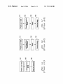
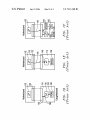
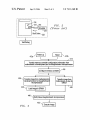
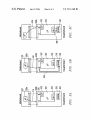
1
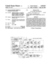
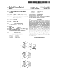
US0071 l l 160Bl
(12) United States Patent
Henniger et al.
(54)
(10) Patent N0.:
(45) Date of Patent:
METHOD AND APPARATUS FOR USING A
DEVELOPMENT PORT FOR BOOT UP
6,003,130 A *
6,105,136 A *
6,161,177
(75) Inventors: Mick Henniger, Austin, TX (US);
(US); Ming Chi Chen, Union City, CA
(US); Ramesh Srinivasan, Santa Clara,
CA (US); Severin Baer, Cupertino, CA
(US); Sanjoy Dey, Fremont, CA (US);
Smita Kiran Rane, Sunnyvale, CA
(Us)
(73) Assignee: Cisco Technology, Inc., San Jose, CA
(Us)
Notice:
Subject to any disclaimer, the term of this
patent is extended or adjusted under 35
USC 154(b) by 0 days.
(22)
(51)
Int. Cl.
12/2000
6,449,732 B1 *
9/2002
(52)
(58)
370/395.1; 361/724, 725; 709/200
See application ?le for complete search history.
OTHER PUBLICATIONS
Code TAP® for the Motorola® MPC8XX; Apr. 1997; cover sheet,
Chapter 14OvervieW, pp. 1-7 through 1-8 and Chapter
44Connecting to the Target, pp. 4-1 through 4-11.
Motorola MPC860 User’s Manual; Figure 1-1.MPC860 Block
Diagram, Section 4iReset pp. 4-1 through 4-11 and Support
Development pp. 18-20 through 18-40.
* cited by examiner
Primary ExamineriJeiTrey Gaf?n
Assistant ExamineriHassan Mahmoudi
(74) Attorney, Agent, or Firm4Campbell Stephenson
ABSTRACT
mation can include information used for con?guring a port,
other than the development port, and/or for con?guring a
memory controller, such as for a daughterboard DRAM. Use
of the Debug port makes it possible to reduce or eliminate
the need for storing boot-up code or con?guration informa
tion on a daughterboard ROM, or other non-volatile
memory, thus reducing cost and space requirements, poWer
consumption and the like.
References Cited
U.S. PATENT DOCUMENTS
Tehranian et al.
713/2
........ .. 714/12
con?guration information from a motherboard for use in
713/201, 400; 714/25, 30, 12; 710/302;
3/1999
Rasmussen et al.
. . . . ..
boot-up. In various aspects, the code or con?guration infor
US. Cl. ......................... .. 713/2; 713/200; 709/200
Field of Classi?cation Search .................. .. 713/2,
5,878,248 A *
713/201
. . . . . . . . . . . .
The development port or Debug port of a microprocessor on
an intelligent daughterboard is used for downloading code or
(2006.01)
(2006.01)
(56)
Anderson
Applied Microsystems Corporation; Emulator Installation Guide;
(57)
Feb. 7, 2000
G06F 9/44
G06F 15/16
Anderson .................... .. 713/2
Ascolese LLP
(21) Appl. N0.: 09/499,598
Filed:
Sep. 19, 2006
8/2000 Cromer et a1. .
*
Kelvin Shih-Tai Liu, Culpertino, CA
A
12/1999
US 7,111,160 B1
14 Claims, 4 Drawing Sheets
........ .. 709/200
Motherboard
/______
U.S. Patent
2896
Sep. 19, 2006
m1
n
31;
_1
m
Sheet 2 of4
lzéoQ1
__
T
2
E
US 7,111,160 B1
3%
é
t
d
c
$12
@EE
2896
6D~m:
3%E E
6E5
12E%5
NNF
2896
m1
28 :?
U.S. Patent
Sep. 19, 2006
m
“ /./.
P_m
m
m
m
u
u
n
P
_
mml-mm
Sheet 3 of4
FD”rrwGT 2Aw
m
x"
m
6 2"nH
2mm
m
”ME mm
:n:u.ow.
_
0
_
US 7,111,160 B1
/\
Test/Debug
Reset
\ 412b
/ 414
Transfer memo
rly controller configuration informatjon from
motherboard to deve opment port on aughterboard mlcroprocessor
Con?gure memory controller /
436
\
4
rtbeor8.0mwmm
h
g
r
e
p
r
0
8
%
‘aLlsrm
o0 anm.|gmtrnlo a00 .nr9 mmcnmdeD Meh
mme
.ld nV86
gI"pI
\we
00.|
416
Tommne‘mm.nwmmmD WVMea ?m\_0S4mm4
m
mtuo
6
1
(Soft) Reset daughterboard microprocessor
452
FIG. 4
\
\ Em“ te image
U.S. Patent
28 6
/
E826:
/
Sheet 4 of4
US 7,111,160 B1
vm /
mi‘11 0.2
/
11
9m
28 62
Sep. 19, 2006
28 59
um65%
£852
.mmQDN
ESQ
.3mQPN
35/
8%
3L"
m
31L"
_
_
?
ll
m1
.02
52 a
US 7,111,160 B1
1
2
METHOD AND APPARATUS FOR USING A
DEVELOPMENT PORT FOR BOOT UP
cessor (Which is a port that is normally inactive or not used
during poWer-up, boot-up, reset or during normal operation)
is used to facilitate one or more of the boot-up procedures,
such as accessing or storing boot-up code, con?guration
information and the like, originating on (or received from)
the motherboard (or other component of the electronic
device). In one embodiment, the development port is used
only for doWnloading or accessing the minimum amount of
boot code (or the like) needed or useful for initially booting
The present invention is related to employing a develop
ment port of a microprocessor for boot procedures and in
particular to reduce or avoid the need for relying on a read
only memory (ROM) or similar device for boot up.
BACKGROUND INFORMATION
or con?guring the daughterboard components. In one
It is common for microprocessor-based electronic equip
embodiment, initial code doWnloaded, via the development
ment to include tWo or more interconnected printed circuit
port, includes code as needed for con?guring a memory
boards, often including a main circuit board having the main
controller or microprocessor (often termed the “mother
controller and/or other devices permitting operation of a
DRAM. Thereafter, additional operating system or other
code is imported into daughterboard memory via more
conventional routes. In another embodiment, the develop
ment port is used for doWnloading, onto the daughterboard,
some or all of the operating system (or the so-called
board”) and one or more connected “daughterboards”. In
many electronic devices, some or all of the daughterboards,
may, themselves, be “intelligent”, i.e., may have their oWn
programmable controllers, typically microprocessors.
When electronic devices of these types are operated, upon
initial poWer-up (or, in some cases, upon resetting the
“image”) used for normal operation of the daughterboard.
20
BRIEF DESCRIPTION OF THE DRAWINGS
microprocessors) some or all devices on the boards need to
access and/or execute certain microcode or other code or
con?guration information. Some or all of this code or
information may include What is commonly called “boot-up
code”. Because such boot-up code must be available, (eg
FIGS. 1A and ID are a How diagram and a block diagram,
respectively, depicting procedures and components for boot
25
upon poWer-up), it is often stored in a read only memory
FIGS. 1B and 1E are a How diagram and a block diagram,
(ROM) device mounted on the same board Where the
microprocessor is mounted. Although ROM components are
commonly provided for this purpose, it is, at least theoreti
cally, possible to use any type of non-volatile memory, such
respectively, depicting procedures and components for boot
30
respectively, depicting procedures and components for boot
In many situations, providing or mounting a separate
ROM (or other non-volatile memory) component on an
35
up With respect to an intelligent daughter card according to
one previous approach;
FIG. 2 is a block and How diagram depicting components
and procedures using a Debug port for testing or Debug
purposes according to previous approaches;
a daughterboard occupies surface area on the board Which is
often needed for accommodating other components or cir
cuitry (particularly since many daughterboards have rela
tively small surface area). Furthermore, the ROM compo
nents themselves undesirably add to the cost of the
up With respect to an intelligent daughter card according to
one previous approach;
FIGS. 1C, and IF are a How diagram and a block diagram,
as ?ash memory, SRAM and the like.
intelligent daughterboard is a non-optimal approach to pro
viding boot-up code. The mounting of a ROM component on
up With respect to an intelligent daughter card according to
one previous approach;
FIGS. 3A, B and C are block diagrams depicting proce
40
daughterboard and the cost of mounting such ROM devices
undesirably adds to the cost of board fabrication. ROM
devices undesirably consume poWer. Furthermore, ROM
dures for daughterboard boot-up according to embodiments
of the present invention; and
FIG. 4 is a How chart depicting steps in a boot-up
procedure of an intelligent daughterboard according to an
embodiment of the present invention.
devices and similar memory devices may be cumbersome or
impossible to reprogram, e.g., to accommodate upgrades and
the like. Accordingly, it Would be useful to provide a system,
method and apparatus for use in booting up an intelligent
daughterboard While eliminating or reducing the need for
DETAILED DESCRIPTION OF THE
PREFERRED EMBODIMENT
Before describing aspects of the present invention, certain
previously-used approaches Will be described. As depicted
mounting a ROM or other nonvolatile memory on the
daughterboard.
50
Cost is often a consideration in designing and implement
ing electronic devices and, although there are advantages
(noted above) to avoiding the need for mounting nonvolatile
memory on a daughterboard, the cost for such an approach
can be a signi?cant issue. Accordingly, it Would be useful to
provide a system, method and apparatus to reduce or avoid
112, an intelligent daughterboard 114 (i.e. having a micro
processor or similar controller 116), Which is coupled to a
motherboard 118 (typically via an edge connector 122) Will
55
have a microprocessor 116 Which receives boot code 124
from a non-volatile memory such as a ROM 126 mounted on
the daughterboard. In a typical situation, the daughterboard
the need for mounting nonvolatile memory on an intelligent
daughterboard in Which at least some of the components or
processor 116 includes a serial or other port 128 coupled to
a bus 132. HoWever, in typical previous devices, it is
features involved are components and features Which are
already present, eg for another purpose.
in FIGS. 1A and 1D, according to at least some previous
approaches, upon poWer up (or reset) of an electronic device
60
necessary to use the boot code 124 to con?gure the serial
port 128 before receiving information from the motherboard
SUMMARY OF THE INVENTION
118 over the bus 132. For this reason, in the con?guration
depicted in FIG. 1D, it is impossible to doWnload the boot
The present invention includes the recognition of the
existence, nature and/or source of problems in previous
approaches, including as described herein. According to one
aspect, the development port of a daughterboard micropro
code 124 from the motherboard 118 over the bus 132, since
65
the daughterboard 128 cannot be con?gured until after the
boot code 124 has been accessed. As noted above, the need
for providing a nonvolatile memory 1.26 mounted on the
US 7,111,160 B1
3
4
daughterboard 114 undesirably increases costs, occupies
to reduce or avoid the need for mounting a ROM component
board surface area, consumes power, and may make it
(or other non-volatile memory component) on the daugh
cumbersome or impossible to provide programming
terboard.
upgrades.
Many types of microprocessors provide a development
port or debug port. One example is the development port
provided in the Motorola MPC860 microprocessor and
described, e.g., in MPC860 PoWer QuiccTM user’s manual,
especially at pages 4*1 through 4*12 and 18*22, 18410,
incorporated herein by reference. Regardless of What it may
After the boot code 124 is provided from the ROM 126,
the port 128 can be con?gured thus permitting the operating
system or “image” to be loaded 134 (FIG. 1A), typically
from the ROM 126 (FIG. 1D)(e.g. a PROM or from a ?ash
memory). As described beloW, in other con?gurations, the
be called in other contexts, as used herein, a development
port or Debug port of a microprocessor is a port Which does
not need con?guration, folloWing a poWer-up or (soft) reset,
in order to load or receive data provided at the port. In the
image can be doWnloaded through the interface betWeen the
host and the daughtercard. Thereafter, the microprocessor
116 can be reset and the operating system or image can
execute 136 (FIG. 1A).
present context, a soft reset Will cause the image to start
In the approach of FIGS. 1B and 1E, a daughterboard
Which contains a memory other than (or in addition to) a
executing at the reset vector in DRAM. In the example of the
MPC860, the development port is a dedicated serial port
Which does not need any of the regular system interfaces. In
dynamic random access memory (DRAM) storage device,
such as a static random access memory device (SRAM) 138.
the example of the MPC860, the development port provides
In the approach of FIG. 1B, folloWing poWer up or reset 112
the processor 142 (FIG. IE) on the motherboard (or “host”)
118 provides ?rmWare or microcode image for doWnloading
20
144, e.g., via a serial or other bus 146 to the non-DRAM
cessor is inactive or not used during normal operation of the
electronic device and also is typically inactive or not used
during poWer-up or boot-up procedures in an electronic
storage device 138 on the daughter card 114 (via an interface
betWeen the host and the card). Following the image doWn
load, the processor on the daughter card 114 is reset 148
(FIG. 1B), after Which it executes the image 152.
Unfortunately, the con?guration depicted in FIGS. 1B and
25
DRAM 154, for proper operation, needs to be coupled to or
and the like. In a typical use, a Debug port 212 (FIG. 2) of
a microprocessor 214 is connected, via a ribbon connector,
30
Applied Microsystems Corporation, and described, for
35
gate array or the like) or, in some cases, may be built-in as
part of the microprocessor 116. In either case, hoWever, the
memory controller 156 must be typically con?gured before
it can control the DRAM 154. Accordingly, in the con?gu
Debug port during normal operation of an electronic device
by an end user. When an emulator 218 is coupled to a Debug
port 212, it is possible to use the emulator 218 to load data
1C), microcode or con?guration information 158 (FIG. 1F)
is provided to (or accessed by) the microprocessor 116 from
cost, occupying surface area, consuming poWer and making
it impossible or cumbersome to provide updates. In the
approach of FIGS. 1C and IF, after the memory controller
has been con?gured, the image or operating system can be
doWnloaded, eg from the motherboard 144 for storage 164
in the DRAM 154. Thereafter, the microprocessor 116 is
reset 166 (FIG. 1C) and the image stored in the DRAM 154
to the Debug port 212 and, if desired, it Would be possible
to use an emulator 218 to doWnload boot code 222 to the
Debug port 212.
45
50
55
interface to the motherboard 316, eg through an edge
60
connector 3281). In one embodiment, on the daughterboard
318, the bus 326 comprises a plurality of traces or leads
formed on the surface of the printed circuit board 318 in a
manner that Will understood by those of skill in the art. With
respect to the motherboard 316, in one embodiment, a serial
peripheral device connection is used, at least during boot up,
processors Which is provided for testing or debugging pur
referred to as a “Debug port”) can play a role in boot-up of
an intelligent daughterboard, in particular, in such a Way as
controller con?guration information, is doWnloaded 314
(FIG. 3A) from a motherboard 316 to a coupled daughter
board 318 through the development port 322 of the daugh
terboard microprocessor 324. In the embodiment depicted in
FIG. 3A, a bus (or other) communication line 326 is pro
vided betWeen the development port 322 and a connection or
nition that a component or feature of many types of micro
poses, namely the development port (DP) (sometimes
(FIG. 4) initial boot-up code (or con?guration information),
Which can, in at least one embodiment, include memory
memory component or device 126 (FIGS. 1D and F), 138
(FIG. 1E) (such as a PROM or an SRAM) on the daugh
terboard 114. SRAMs and similar devices are generally
disadvantagous at least because of their relatively high cost,
and poWer and space requirements.
One aspect of the present invention involves the recog
One aspect of the present invention involves using the
Debug port of a daughterboard microprocessor during nor
mal use by an end user and, in particular during normal
boot-up, such as folloWing poWer-on or reset. As depicted in
FIGS. 3AiC and 4, folloWing poWer-up or reset 412a,b,
is executed 168.
Thus, as can be seen from FIGS. 1A through F, in the
depicted previous approaches, it Was typically necessary to
provide some type of non-DRAM, typically non-volatile,
example, in “Emulator Installation Guide, Code TAP for the
Motorola MPC8XX”, particularly pages 1*7, 21*8 and
4il24ill, incorporated herein by reference. An emulator
218 is typically used for testing the above unit, or other
development purposes, and is typically not coupled to a
ration of FIGS. 1C and IF, upon poWer up or reset 112 (FIG.
a ROM 126 (or other nonvolatile memory) and then pro
vided 162 to the memory controller 156. Thus, in the
embodiment of FIG. 1C, a ROM 126 is used, increasing
cable or the like, 216 to an external emulator device 218. An
example of an external emulator device of a type that can be
used in connection With the MPC860, for example, is that
sold under the trade name Code TAPTM, available from
controlled by a memory controller 156 (FIG. 1F) (eg to
provide it With timing information and the like). A memory
controller 156 can be provided externally in hardWare (eg
using a programmable logic device or a ?eld programmable
device. Instead, the development port is generally used
during product design or development, testing, debugging
IE is not feasible When the target device on the daughter
card (for storing the image) is DRAM 154 (as depicted in
FIG. 1F). In the approach depicted in FIGS. 1C and IF, the
a full duplex serial interface. The physical connections for
using the development port in the MPC860 include a 10-pin
connector. Typically, the development port of a micropro
65
for providing a path to doWnload information codes, con
?gurations and the like stored on the motherboard (eg in a
memory device mounted on or coupled to the motherboard).
US 7,111,160 B1
5
6
In the embodiment depicted in FIGS. 3AiC, the memory
controller 332 is provided as a component of the micropro
cessor 324, although, as noted above, it is also possible to
using it for con?guring a memory controller. The present
invention can be used in any of a plurality of different types
or categories of electronic devices, including personal com
puters, Work stations, netWork devices such as routers,
sWitches, bridges, hubs and the like, telecommunications
use the present invention in con?gurations in Which a
memory controller is provided as an external device. The
information Which Was doWnloaded 414 is used to con?gure
416 the memory controller 322. Once the memory controller
devices or components and the like.
retically, operable. In one embodiment (FIG. 3C), folloWing
con?guration of the memory controller 332, further coding
The present invention, in various embodiments, includes
components, methods, processes, systems and/or apparatus
substantially as depicted and described herein, including
various embodiments, subcombinations, and subsets
or softWare, such as an operating system or “image” is
thereof. Those of skill in the art Will understand hoW to make
332 has been con?gured, the DRAM 334 is, at least theo
doWnloaded 336 (step 436) through the development port
and use the present invention after understanding the present
322 for transfer 338 to the DRAM 334. In another embodi
ment (FIG. 3B), image or other code can be transferred 342
from the motherboard and provided 446 to the DRAM 334
disclosure. The present invention, in various embodiments,
includes providing devices and processes in the absence of
items not depicted and/or described herein or in various
by using a system bus 346 i.e. Without using the develop
embodiments hereof, including in the absence of such items
ment port 322 for the transfer of the image or the operating
system. In any case, after the operating system or image has
been stored in the DRAM 334, the daughterboard micro
processor can be (soft) reset 448 and the image can be
executed 452.
as may have been used in previous devices or processes, eg
for improving performance, achieving ease and/or reducing
20
As can be seen from FIGS. 3A£, use of the development
port 322, as described, makes it possible to provide for
con?guration or boot up of an intelligent daughterboard in
the absence of a need for using a ROM or other non-volatile
25
memory mounted on the daughterboard. The depicted
cost of implementation. The present invention includes
items Which are novel, and terminology adapted from pre
vious and/or analogous technologies, for convenience in
describing novel items or processes, do not necessarily
retain all aspects of conventional usage of such terminology.
The foregoing discussion of the invention has been pre
sented for purposes of illustration and description. The
foregoing is not intended to limit the invention to the form
or forms disclosed herein. Although the description of the
embodiments include a DRAM mounted on the daughter
board, but typically, a DRAM Would be provided for use
invention has included description of one or more embodi
during non-boot up general operation of the daughterboard
ments and certain variations and modi?cations, other varia
tions and modi?cations are Within the scope of the invention,
eg as may be Within the skill and knoWledge of those in the
and accordingly does not represent an additional cost, con
sumption of poWer or surface area and the like (compared to
the poWer, surface area and cost needed for non-boot-up
30
art, after understanding the present disclosure. It is intended
operation). As noted above, a Debug port is commonly
provided on microprocessors (for other purposes) and thus
this component or feature used during embodiments of the
to obtain rights Which include alternative embodiments to
the extent permitted, including alternate, interchangeable
35
present invention also is a component or feature Which is
already present for other purposes and thus is compatible
With providing embodiments of the present invention With
out the need to design or provide additional components. In
at least some embodiments, communication of code or data
40
from the motherboard to the daughterboard development
port is performed using the motherboard’s serial peripheral
device connection, coupling or pathWay, also already present
(on the motherboard) for another purpose, thus in assisting
in avoiding the need for incurring additional design or
component costs in order to implement embodiments of the
present invention.
In light of the above description a number of advantages
of the present invention can be seen. The present invention
makes it feasible to achieve con?guration and/or boot up of
and/or equivalent structures, functions, ranges or steps to
those claimed, Whether or not such alternate, interchange
able and/or equivalent structures, functions, ranges or steps
are disclosed herein, and Without intending to publicly
dedicate any patentable subject matter.
What is claimed is:
1. A method of booting up a system, Wherein the system
comprises a motherboard coupled to daughterboard, Wherein
the daughterboard comprises a microprocessor, a system
bus, a random access memory that stores a copy of an
45
operating system, and a second bus, Wherein the micropro
cessor comprises a development port coupled to the second
bus, Wherein the microprocessor comprises a memory con
troller, Wherein the memory controller is coupled to the
random access memory via the system bus, the method
50
comprising:
transmitting memory controller con?guration information
an intelligent daughterboard While reducing or eliminating
the need for using and/or mounting a ROM or other non
from said motherboard to said memory controller via
volatile memory device on the daughterboard. The present
invention accordingly can reduce the cost, consumption of
surface area and/or consumption of poWer on the daughter
board, needed for boot up or con?guration purposes, e.g.
the development port and the second bus, in response
to a poWer-on or reset of said system; and
55
providing additional surface area Which can be used mount
ing other circuitry or components. The present invention
the memory controller con?guration information via
the development port and in response to the poWer-on
effectively makes use of one or more features or components
Which are provided or used for other purposes, thus making
it possible to implement at least some embodiment of the
the memory controller reading some or all of the operat
ing system copy stored in the random access memory
via the system bus after the memory controller receives
60
or reset of said system.
present invention Without undue requirements for adding
2. The method of claim 1 transmitting the copy of the
operating system from the motherboard to the random
additional components to an electronic device.
access memory for storage therein.
The number of variations and modi?cations of the inven
tion can be used. It is possible to use some aspects of the
invention Without using others. It is possible to use the
development port during daughterboard boot up Without
65
3. The method of claim 1 Wherein the development port
comprises a full duplex serial interface.
4. The method of claim 1 further comprising transmitting
the operating system copy from the motherboard to the
US 7,111,160 B1
7
8
random access memory for storage therein via the develop
ment port, after the memory controller receives the memory
9. The apparatus of claim 7 Wherein the development port
is con?gured to transfer the con?guration information auto
controller con?guration information via the development
matically, in response to a poWer up or a reset of the
port and in response to the poWer-on or reset of said system.
5. The method of claim 4 Wherein the memory controller
con?guration information is transferred to the memory con
apparatus.
10. The apparatus of claim 9 Wherein the memory con
troller is con?gured to read some or all of the operating
system copy stored in the random access memory after the
troller from a memory device on said motherboard.
6. An apparatus comprising:
memory controller receives the con?guration information
a ?rst printed circuit board;
a processor mounted to the ?rst printed circuit board,
Wherein the processor comprises a development port
and in response to the poWer up or the reset of the apparatus.
11. The apparatus of claim 10 Wherein the development
port comprises a full duplex serial interface.
12. The apparatus of claim 6 Wherein the second bus
and a memory controller;
a system bus formed on the ?rst printed circuit board and
coupled to the memory controller;
comprises a serial data bus.
a second bus formed on the ?rst printed circuit board and
coupled to the development port;
13. An apparatus comprising:
a random access memory mounted on the ?rst printed
a ?rst printed circuit board coupled to a second printed
circuit board and coupled to the memory controller via
the system bus, Wherein the random access memory
stores a copy of an operating system;
circuit board;
20
a processor mounted to the ?rst printed circuit board,
Wherein the development port is con?gured to transfer
con?guration information to the memory controller;
Wherein the processor comprises a development port
Wherein the memory controller is con?gured to read some
or all of the operating system copy stored in the random
access memory via the system bus after the memory
a random access memory mounted on the ?rst printed
circuit board and con?gured to store a copy of an
and a memory controller;
25
controller receives the con?guration information via
the development port.
7. The apparatus of claim 6 further comprising:
a second printed circuit board;
a ?rst data storage device mounted on the second printed
controller;
30
circuit board, Wherein the ?rst data storage device
of the processor.
8. The apparatus of claim 7 Wherein the development port
receives data from an emulator device external to the pro
cessor When the development port is coupled to the emulator
device.
a second bus coupled to the development port, Wherein
the second bus is formed on the ?rst printed circuit
board;
stores the con?guration information;
a coupler, coupling the ?rst printed circuit board to the
second printed circuit board, de?ning at least a ?rst data
communication path from said second printed circuit
board to said ?rst printed circuit board;
Wherein the con?guration information can be transmitted
from the ?rst storage device, over the ?rst communi
cation path, said second bus, to said development port
operating system;
a system bus formed on the ?rst printed circuit board and
coupled to the random access memory and the memory
35
means for doWnloading memory controller con?guration
information from said second printed circuit board to
said memory controller via the development port and
the second bus, in response to a poWer on or reset of
said apparatus.
14. The apparatus of claim 13 Wherein the development
port receives data from an emulator device external to the
processor When the development port is coupled to the
emulator device.