1
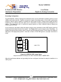
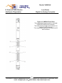
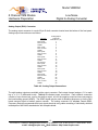
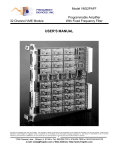
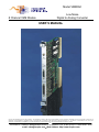
Model VM8DAC
Low Noise
Digital to Analog Converter
8 Channel VME Module
USER’S MANUAL
We hope the information given here will be helpful. The information is based on data and our best knowledge, and we consider the information to be true and accurate. Please read all
statements, recommendations or suggestions herein in conjunction with our conditions of sale which apply to all goods supplied by us. We assume no responsibility for the use of these
statements, recommendations or suggestions, nor do we intend them as a recommendation for any use which would infringe any patent or copyright.
1
25 Locust St., Haverhill, Massachusetts 01830 • Tel: 800/252-7074, 978/374-0761 • FAX:978/521-1839
e-mail: [email protected] • Web Address: http://www.freqdev.com
Model VM8DAC
8 Channel VME Module
Contents, Figures and Tables
Low Noise
Digital to Analog Converter
Contents
1. Introduction ...............................................................................................................................................4
Features/Benefits ..............................................................................................................................4
2. Specifications............................................................................................................................................5
3. Description................................................................................................................................................6
VMEBus Interface .............................................................................................................................6
Master Clock Interface and Timebase Control Logic ........................................................................6
DAC/Amplifiers and Output Connections ..........................................................................................7
External Power Supply Interface.......................................................................................................7
4. Hardware Preparation...............................................................................................................................8
Unpacking and Inspection.................................................................................................................8
Hardware Configuration ....................................................................................................................9
VMEbus Base Address .....................................................................................................................9
Grounding Configuration .................................................................................................................11
Board Installation ............................................................................................................................12
I/O Connections and the Front Panel..............................................................................................12
Clock Input Connector.....................................................................................................................14
External Power Supply Connector ..................................................................................................14
Analog Output (DAC) Connector.....................................................................................................16
5. Programming ..........................................................................................................................................17
Memory Map and Register/Bit Descriptions....................................................................................17
Programming the Timebase............................................................................................................19
DAC Data Write Timing and Constraints.........................................................................................19
Synchronizing with the Sample Clock .............................................................................................19
6. Troubleshooting and Technical Support .................................................................................................21
7. Warranty Information ..............................................................................................................................22
Limitation of Liability........................................................................................................................22
8. Ordering Guide .......................................................................................................................................23
Figures
Figure 3-1: A VM8DAC Channel...................................................................................................................6
Figure 4-1: VM8DAC Base Address Configuration Jumpers. .......................................................................9
Figure 4-2: VM8DAC GND Jumper Setup. .................................................................................................10
Figure 4-3: VM8DAC Front Panel ...............................................................................................................12
Figure 4-4: VM8DAC External Power Supply Connector............................................................................14
Figure 5-1: VM8DAC VMEbus Memory Map. .............................................................................................17
Figure 5-2: VM8DAC Board Data Transfer Timing. ....................................................................................19
Tables
Table 4-1: External Power Supply Connections. ........................................................................................13
Table 4-2: Analog Output Connections.......................................................................................................15
2
25 Locust St., Haverhill, Massachusetts 01830 • Tel: 800/252-7074, 978/374-0761 • FAX:978/521-1839
e-mail: [email protected] • Web Address: http://www.freqdev.com
Model VM8DAC
8 Channel VME Module
Introduction
Low Noise
Digital to Analog Converter
1. Introduction
The VM8DAC VMEbus digital to analog converter (DAC) board from Frequency Devices Inc. offers eight
channels of precision low-distortion/low-noise digital to analog converters that operate with a sample clock
frequency generated from a software programmable differential input external clock master timebase
divider. The boards are available in a single width B-size (6U) VME form factor and fully conform to
VMEbus Revision C.1 as an A32/D32 Data Transfer Bus Slave.
VM8DAC’s provide high resolution (24-bit) and low resolution (16-bit) data access to on-board DAC’s. The
boards interpret the received parallel data from the VMEbus as binary 2’s complement. This data is
serialized and transferred to any selected DAC channel at a fixed master timebase where it is converted to
analog signals at a software programmable sampling rate. The DAC channels may be configured to
16,384, 8,192, 4,096, or 2,048 samples per second.
Features/Benefits
•
Eight discrete channels with programmable sampling that provide a 24- bit DAC stage for each channel
offers the user versatile and convenient digital to analog conversion.
•
Outputs synchronized to the front panel external clock allow for multi-card synchronicity.
•
Designed for Real Time Operating Systems (RTOS) to provide minimal pipeline delay (less than 5
microseconds). i.e. Linux or Vx Works.
•
Interrupt free operation provides glitch energy of <5nV-sec and extremely low noise density
(<100nV/ Hz ).
•
VME backplane is galvanically isolated from the analog section to reduce system integration problems.
3
25 Locust St., Haverhill, Massachusetts 01830 • Tel: 800/252-7074, 978/374-0761 • FAX:978/521-1839
e-mail: [email protected] • Web Address: http://www.freqdev.com
Model VM8DAC
8 Channel VME Module
Specifications
Low Noise
Digital to Analog Converter
2. Specifications
(@ 25oC and Rated Power Input)
Module Size/Dimensions
1. Standard 6U VME, single slot module
2. Weight
Connectors
3. Input clock connector
4. Analog output connector
5. Matching output connector
External Clock Input
6. Configuration
7. Isolation
8. Frequency
Analog output
9. Number of channels per board
10. Analog output configuration
11. Minimum output load
12. Maximum output voltage
13. Output amplifier 3 dB bandwidth
14. Output impedance
15. Anti-image filter
16. Inter-channel crosstalk
DAC specifications
17. Number of bits
18. Binary number format
19. Sampling rate
20. Bipolar zero error
21. Bipolar zero error drift
22. Glitch energy
23. Output-referred noise
24. Amplitude match and accuracy
25. Harmonic spikes
26. Output settling time to 1%
Power requirements
27. From the + 5V VME backplane supply
28. From the +/- 12V VME backplane supply
VME interface
29. Interface configuration
30. Address modifier lines decoding
31. Data word size
32. Bus cycle compatibility
33. Addressing modes
Environmental
34. Operating Temperature range
35. Storage Temperature range
36. Humidity
9.17 X 6.3 inches (233 X 160 mm)
~ 1 lb., 0.45 kg
Lemo EPG.OB.302.HLN
Male DB25
Female DB25
Differential, TTL compatible
Transformer isolated
222 Hz (4.194305 MHz)
8
Differential
500 ohm
± 10V into 10 kOhm
>50KHz
50 ohms per leg
None
< -90dB (frequencies less than 50KHz)
24 bits
Binary 2’s complement
16,384, 8,192, 4,096, 2,048 samples per second
±2% F.S. maximum
± 5 ppm of FS/ °C
< 5nV-sec
<100nV/vHz
(40 Hz to 8192 Hz with FS 1000 Hz sine wave)
± 0.1 dB
<-100 dB (referred to a full scale output signal )
< 5 microseconds (From output clock edge)
1.0 A Max.
1.0 A
A32/D32 VME Data Transfer Bus (DTB) Slave
Full decode (0x09, 0x0A, 0x0D, and 0x0E valid)
Long word (Quad Byte) and aligned word (Double Byte)
AO, RMW, bus cycles address pipelining
A32 (Extended) addressing only
0oC to +70oC
-25oC to +85oC
0-95% non-condensing
4
25 Locust St., Haverhill, Massachusetts 01830 • Tel: 800/252-7074, 978/374-0761 • FAX:978/521-1839
e-mail: [email protected] • Web Address: http://www.freqdev.com
Model VM8DAC
8 Channel VME Module
Hardware Preparation
Low Noise
Digital to Analog Converter
3. Description
The VM8DAC is a single width B-size (6U) VME module that consists of a motherboard offering eigth
differential output DAC channels. The motherboard is divided into a VME-grounded digital section and a
galvanically isolated analog section. The “digital section” includes the VMEbus-to-DAC interface, the
master clock interface, and the timebase control logic. The “analog section” contains the opto-isolated high
precision DAC/amplifiers, the external power supply interface, and output connections.
VMEBus interface
The VM8DAC appears on the VMEbus as a Revision C.1 compliant A32/D32, VME Data Transfer Bus
(DTB) Slave with full decoding of address modifier lines. The board supports long word (Quad Byte) and
aligned word (Double Byte) transfers and is compatible with Address Only (AO) and Read-Modify-Write
(RMW) bus cycles as well as with address pipelining. An on-board field programmable gate array (FPGA)
is hard-coded to allow the board to respond to address modifier codes 0x09, 0x0A, 0x0D, and 0x0E. The
board assumes A32 (Extended) addressing and does not respond to A24 (Standard) or A16 (Short) bus
address cycles.
The VM8DAC board does not support Block Transfers (BLT), unaligned transfers, byte transfers, the VME
Serial Bus (VSB), or any features of VME64 or later enhancements. The board does not provide bus
mastering (DMA) capability or interrupt capability, however it is fully compatible with systems that make
extensive use of DMA and interrupts.
The VMEbus backplane offers a software programmable interface to set the actual sample clock frequency
of each DAC channel. Through the interface any user can set a programmable timebase divider, readback
a control word to determine when the board is ready for more data, and send digital signal data.
The board uses an indexed channel addressing scheme to serialize VME digital signal data and transfer it
to the selected DAC/amplifier channel. Figure 3-1 is a simplified block diagram of the VM8DAC showing
one DAC/amplifier channel and all of the common functions.
Master Clock Interface and Timebase Control Logic
The VM8DAC provides a Differential/TTL-compatible/Transformer-isolated external clock input. The
board’s timebase is derived from an 222 Hertz (4.19304 MHz, nominal) external clock that is brought onto
the board over the front panel. On board logic divides this timebase clock by four to provide a board level
master timebase of 220 Hz (1.048576 MHz, nominal). The sample clock pulse width is fixed at one cycle of
this on board master timebase (approximately 954 nanoseconds, nominal). In addition, a software
programmable divider, further divides the master timebase to provide the actual sample clock frequency.
Refer to the external time base select coding in Figure 5-1 in the programming section.
5
25 Locust St., Haverhill, Massachusetts 01830 • Tel: 800/252-7074, 978/374-0761 • FAX:978/521-1839
e-mail: [email protected] • Web Address: http://www.freqdev.com
Model VM8DAC
8 Channel VME Module
Hardware Preparation
Low Noise
Digital to Analog Converter
DAC/Amplifiers and Output Connections
The DAC/amplifiers are located on the analog section of the VM8DAC. Each channel contains two pairs of
DAC’s and one pair of I/V converter/amplifiers.
DAC's
I/V's
Data
WCLK
BCLK
Invert
D
W
B
Out
I
D
W
B
Ch x OUT
PLUS
Out
I
D
W
B
Out
I
D
W
B
Ch x OUT
MIN
Out
I
Figure 3-1: A VM8DAC Channel.
X represents the channel number of 1 up to 8.
The VME-DAC interface generates the inputs to the DAC’s. The inputs to the DAC’s are a bit clock, a word
clock , and the serial data. The serial data is connected in a non-inverting fashion two one pair of DAC’s
and in an inverting fashion to the other DAC pair. This converts the output to a differential one. The output
of each DAC’s pair is connected to an I/V converter amplifier which provides low output impedance. The
output of each I/V converter pair is sent to he output connector as the specific channel’s low impedance
differential signal.
External Power Supply Interface
An external power supply interface provides the option of using external power supplies connected through
a DB15 female connector located on the front panel. Using external power supplies results in lower
common mode noise as all power is derived from external sources and not from the VME backpanel.
6
25 Locust St., Haverhill, Massachusetts 01830 • Tel: 800/252-7074, 978/374-0761 • FAX:978/521-1839
e-mail: [email protected] • Web Address: http://www.freqdev.com
Model VM8DAC
8 Channel VME Module
Hardware Preparation
Low Noise
Digital to Analog Converter
4. Hardware Preparation
Unpacking and Inspection
Before unpacking the VM8DAC shipping container, carefully inspect the exterior of the package for
evidence of damage. After noting areas of possible shipping damage, open and unpack the shipping
container, being careful to preserve the container and packing materials in case they are needed later.
CAUTION:
The VM8DAC Board is sensitive to STATIC ELECTRICITY.
Use proper GROUNDING TECHNIQUES
when handling the board.
Carefully remove the VM8DAC board from its anti-static bag and visually inspect for evidence of damage.
If the board appears to be damaged in any way, notify the shipping carrier.
7
25 Locust St., Haverhill, Massachusetts 01830 • Tel: 800/252-7074, 978/374-0761 • FAX:978/521-1839
e-mail: [email protected] • Web Address: http://www.freqdev.com
Model VM8DAC
8 Channel VME Module
Hardware Preparation
Low Noise
Digital to Analog Converter
Hardware Configuration
Once the VM8DAC VMEbus board has been removed from its anti-static bag and carefully inspected for
damage, you are ready to configure the board for your particular system.
CAUTION:
The VM8DAC Board is sensitive to STATIC ELECTRICITY.
Use proper GROUNDING TECHNIQUES
when handling the board.
VMEbus Base Address
The selection of DAC channels and the timebase programming is done through VME memory space using
a Base Address that can be set throughout all of A32 space. A VM8DAC board occupies a 256-byte block
in A32 address space and may be configured on any 256-byte boundary. The user will need to set a Base
Address that is appropiate for the VME system in which the VM8DAC will be installed. The factory set
Base Address is 2000(hex). Before attempting to use the board, the user should set/verify the base
address using the address DIP switch blocks SW1, SW2, and SW3 on the board.
To reconfigure the VM8DAC Base Address, lay the board flat as shown in Figure 4-1. See the three DIP
switches that make the 24 position switch block shown in Figure 4-1. This switch block is used to set the
board's base address in A32 address space. SW1 set address lines A24 through A32, SW2 set address
lines A17 up to A23, and SW3 set lines A8 up to A16. A bit switch moved to the right sets a logic '1' while a
bit switch moved to the left sets a logic '0'. For example, to set the VM8DAC Base Adresss to 800(hex),
the bit switch which corresponds to A11 is moved to the right and all the other switches to the left.
8
25 Locust St., Haverhill, Massachusetts 01830 • Tel: 800/252-7074, 978/374-0761 • FAX:978/521-1839
e-mail: [email protected] • Web Address: http://www.freqdev.com
Model VM8DAC
8 Channel VME Module
Hardware Preparation
Low Noise
Digital to Analog Converter
Figure 4-1: VM8DAC Base Address Configuration Jumpers.
An installed jumper sets a logic '1' while a missing jumper sets a logic '0'.
9
25 Locust St., Haverhill, Massachusetts 01830 • Tel: 800/252-7074, 978/374-0761 • FAX:978/521-1839
e-mail: [email protected] • Web Address: http://www.freqdev.com
Model VM8DAC
8 Channel VME Module
Hardware Preparation
Low Noise
Digital to Analog Converter
Grounding Configuration
The DAC/amplifier “analog” signal ground reference point can be connected to chassis ground or to the
VMEbus back plane ground. If neither connection is made, the analog portion of the board is galvanically
floating so that its ground (AGND) is isolated from VME system ground. Floating means signal ground is
isolated from the chassis and back plane and is referenced to external signal ground through the I/O
cables. This allows the user to connect the analog common to other commons without creating low
frequency ground loops.
A set of jumpers is provided to allow the analog common to be connected to either VME system ground or
chassis ground through the board front panel. See Figure 4-2 for ground jumper setup information. To
change the signal ground reference point, locate the ground reference jumper J2 and jumper the ANALOG
GND post to the appropriate position. Note that to select a FLOATING ground, no jumper connection is
made.
NC
CHASSIS
GND
ANALOG
GND
J2
U48 - P.S.
VMEBP
GND
Figure 4-2: VM8DAC GND Jumper Setup.
Jumper the ANALOG GND post to either CHASSIS GND or VMEBP GND.
After the board's base address and grounding has been configured, the board is ready for installation in a
VME system.
10
25 Locust St., Haverhill, Massachusetts 01830 • Tel: 800/252-7074, 978/374-0761 • FAX:978/521-1839
e-mail: [email protected] • Web Address: http://www.freqdev.com
Model VM8DAC
8 Channel VME Module
Hardware Preparation
Low Noise
Digital to Analog Converter
Board Installation
Frequency Devices' eight channel VM8DAC boards conform mechanically, in every respect, to the single
width VME "B" size (6U) form factor. Installation of the board into a standard VME mainframe can proceed
exactly as for any other standard single width "B" size (6U) VME board.
CAUTION:
The VM8DAC Board is sensitive to STATIC ELECTRICITY.
Use proper GROUNDING TECHNIQUES
when handling the board.
The VM8DAC board may be installed in any available mainframe slot except Slot 0 (VMEbus Master). The
board does not use VMEbus interrupts or bus mastering capabilities, but passes all VMEbus daisy chained
signals automatically.
The major considerations in locating the VM8DAC board in the mainframe are for EMI and I/O signal
cabling. To minimize interference from other boards in the system, it is good practice to keep one or more
empty slots between analog signal conditioning boards and high speed digital boards in the system. When
cabling the system, it is desirable to keep the analog signal cabling as short as possible and physically
located away from high speed digital cabling and high voltage switching lines.
I/O Connections and the Front Panel
The following information is provided to assist the user/integrator in installing and interconnecting a
VM8DAC board into a VME system.
Figure 4-3 shows the layout of the VM8DAC front panel. The following sections provide detailed
information about connectors, pinouts, and cabling. There are no front panel indicators or controls on the
VM8DAC.
11
25 Locust St., Haverhill, Massachusetts 01830 • Tel: 800/252-7074, 978/374-0761 • FAX:978/521-1839
e-mail: [email protected] • Web Address: http://www.freqdev.com
Model VM8DAC
8 Channel VME Module
Hardware Preparation
Low Noise
Digital to Analog Converter
Figure 4-3: VM8DAC Front Panel
The external clock input connector is a female
LEMO EPG.OB.302.HLN connector.
The external power supply input connector is a
female 15-pin D connector.
The analog output connector is a male 25-pin Dshell connector.
12
25 Locust St., Haverhill, Massachusetts 01830 • Tel: 800/252-7074, 978/374-0761 • FAX:978/521-1839
e-mail: [email protected] • Web Address: http://www.freqdev.com
Model VM8DAC
8 Channel VME Module
Hardware Preparation
Low Noise
Digital to Analog Converter
Clock Input Connector
The clock input connector is a female right-angled Lemo connector located near the top of the front panel.
The clock input is galvanically isolated from both the VME system ground and the analog ground on the
DAC board through the use of transformer coupling. The board is designed to run with an external clock
set to 222 Hz (4.194304 MHz). This signal must be present for the board to work. The input requires a
5Vp-p signal, polarity not being important, except that all boards in a multi-VM8DAC system must be
wired with identical polarity to maintain synchronicity. The external clock should be connected
between the two contact pins on the Lemo connector. The shell of the connector is connected to the DAC
board analog common.
External Power Supply Connector
The power supply connector is a female DB15 connector located near the center of the front panel. Table
4-1 identifies the power supply connections:
Function
+15V Source
GND
-15V Source
GND
+5V Source
GND
-5V2 Source
-5V Source
Power Supply
Connector
1-8 (J5)
1
2
3
4
5
6
7
8
Function
+15V Load
GND
-15V Load
GND
+5V Load
-5V2 Load
-5V Load
Power Supply
Connector
9-15 (J5)
9
10
11
12
13
14
15
Table 4-1: External Power Supply Connections.
There are two power supply modes of operation: internal and external power supply. For operation with
internal power supply provided through the VM8DAC board, a dummy plug must be installed on J5. The
dummy plug has jumper wires between the internal power sources and the loads. Figure 4-4 shows the
dummy plug jumpers. For external power supply operation, the dummy plug is removed and external
power is connected to the ±15V loads, ±5V loads and analog ground via J5. Figure 4-4 also shows the
external power supply connections to each load.
13
25 Locust St., Haverhill, Massachusetts 01830 • Tel: 800/252-7074, 978/374-0761 • FAX:978/521-1839
e-mail: [email protected] • Web Address: http://www.freqdev.com
Model VM8DAC
8 Channel VME Module
Hardware Preparation
Low Noise
Digital to Analog Converter
Connect external supply
to this column
8
-5V Load
15
-5V Source
8
15
-5V2 Source
-5V2 Load
GND
+5V Load
+5V Source
GND
GND
-15V Load
-15V Source
GND
GND
+15V Load
99
1
1
+15V Source
Dummy
plug
jumpers
Figure 4-4: VM8DAC External Power Supply Connector.
When using internal power supply, a dummy plug must be installed.
Both –5V load and –5V2 load must connect to an external –5 Volt
supply for external power operation.
14
25 Locust St., Haverhill, Massachusetts 01830 • Tel: 800/252-7074, 978/374-0761 • FAX:978/521-1839
e-mail: [email protected] • Web Address: http://www.freqdev.com
Model VM8DAC
8 Channel VME Module
Hardware Preparation
Low Noise
Digital to Analog Converter
Analog Output (DAC) Connector
The analog output connector is a male 25-pin D-shell connector located near the bottom of the front panel.
Analog output connections are as follows:
Function
DAC 0 plus
DAC 0 minus
AGND
DAC 1 plus
DAC 1 minus
AGND
DAC 2 plus
DAC 2 minus
AGND
DAC 3 plus
DAC 3 minus
AGND
No Connect
DAC 4 plus
DAC 4 minus
AGND
DAC 5 plus
DAC 5 minus
AGND
DAC 6 plus
DAC 6 minus
AGND
DAC 7 plus
DAC 7 minus
AGND
Analog Output
Connector
Channels 0-7 (J1)
1
2
3
4
5
6
7
8
9
10
11
12
13
14
15
16
17
18
19
20
21
22
23
24
25
Table 4-2: Analog Output Connections.
The eight analog outputs are available at the output connector. Each output channel swings ± 5 V on each
leg or ± 10 V in differential mode. Table 4-2 indicates proper connection. Each channel connection
consists of up to three wires: one for the positive output, one for the negative output and one connected to
the board analog ground (AGND). The AGND signal may be used for shielding purpose or to tie the DAC
board common signal to another system common. The mating connector is a standard Female DB25.
Frequency Devices recommends that input signals be wired using cable consisting of individually shielded
twisted pairs of #22 AWG stranded wire with complete shield.
15
25 Locust St., Haverhill, Massachusetts 01830 • Tel: 800/252-7074, 978/374-0761 • FAX:978/521-1839
e-mail: [email protected] • Web Address: http://www.freqdev.com
Model VM8DAC
8 Channel VME Module
Programming
Low Noise
Digital to Analog Converter
5. Programming
This section provides essential information and specifications for programming the VM8DAC board over
the VMEbus. The DAC Board VME memory map, programming the timebase, writing DAC data, and
techniques for synchronizing data transfers to the sample clock are all covered. Figures 5-1 and Figure 52 provide a quick reference to the VM8DAC board programming and timing constraints.
Memory Map and Register/Bit Descriptions
The VM8DAC board occupies a contiguous 256 byte block of A32 (Extended) VME memory space and
provides both Non-Privileged and Supervisory access. The base address of the 256 byte block is set by
user accessible DIP switches and is aligned on a 256 byte boundary. Therefore, the board will respond to
A32 Non-Privileged and Supervisory accesses within the address block defined by DIP switch settings
corresponding to A31 down to A8. The DIP switch setting is referred to as the Base Address (BA) and
defines the 24 most significant bits of the 32-bit address block. A typical multi-board configuration might
configure board base addresses in increments of 1 (256 byte block) and then index board accesses in
modulo-256 increments.
In order to provide both high resolution (24 bit) and low resolution (16 bit) data paths to the on-board DACs,
and to provide a control/status interface for the board, the DAC Board subdivides its 256 byte memory
space into three distinct segments. The first segment, beginning at the board’s base address [BA],
consists of 8 contiguous long words (32 bytes) that provide 24 bit data access to each of the 8 on-board
DACs. Word transfers (16 bit data transfers) into this segment will result in unpredictable DAC behavior
and should be avoided. The second segment, beginning at [BA] + 0x20, consists of 4 contiguous long
words (16 bytes) that provide packed, aligned 16 bit data access to two DACs simultaneously. Aligned
word transfers can be made into this segment to provide 16 bit data updates to individual DACs. The third
segment consists of a single 16 bit word located at [BA] + 0x32. This is the CONTROL/STATUS word that
provides fields for programming the timebase and for sensing when the board is ready for more data. The
CONTROL/STATUS word may be accessed as a long word, in which case, the 16 most significant bits
(D31…D16) will read as 0x00.
Figure 5-1 provides a graphical description of the DAC Board memory map. The base address, BA, is the
modulo-256 block address set by the on-board DIP switches. In general, an “X” in an address bit position is
insignificant and ignored. The only exception here is when word (16 bit) accesses are made into the
second memory segment, in which case address bit A1 defines which DAC is being accessed. While this
arrangement provides multiple virtual images of the board address space (e.g., high resolution access to
DAC_0 can be made at [BA] +0, [BA] +0x40, [BA] + 0x80, and [BA] + 0xC0), it is recommended that
specific fixed addresses be assigned to the various memory objects.
Referring to Figure 5-1, DAC data is always presented left justified. So in the case of a high resolution
long word write into the first segment, the 8 least significant bits of the 32 bit long word (D7…D0) are
ignored. The VM8DAC board hardware treats all DAC data as 2’s complement. DAC data is “write only”
and will return an indeterminate value, if read. Unimplemented (“X”) bits in the CONTROL/STATUS word
will be ignored when written, but will return ‘0’ when read. Upon power up, the internal timebase is OFF and
the external timebase is disabled, so the board outputs are inactive (cannot be updated). The DAC’s
power up to an unknown state, so establishing the timebase and DAC initialization data should be a high
priority of the start up routine.
16
25 Locust St., Haverhill, Massachusetts 01830 • Tel: 800/252-7074, 978/374-0761 • FAX:978/521-1839
e-mail: [email protected] • Web Address: http://www.freqdev.com
Model VM8DAC
8 Channel VME Module
Programming
Low Noise
Digital to Analog Converter
DAC BOARD VME MEMORY MAP
BASE
ADDRESS
A1
IMPLIED
LSB
A7:A2
BYTE_0
BYTE_1
BYTE_2
BYTE_3
BA:XX0000X(X)
MSB
DAC_0
LSB
XXXXXXXX
BA:XX0001X(X)
MSB
DAC_1
LSB
XXXXXXXX
BA:XX0010X(X)
MSB
DAC_2
LSB
XXXXXXXX
BA:XX0011X(X)
MSB
DAC_3
LSB
XXXXXXXX
BA:XX0100X(X)
MSB
DAC_4
LSB
XXXXXXXX
BA:XX0101X(X)
MSB
DAC_5
LSB
XXXXXXXX
BA:XX0110X(X)
MSB
DAC_6
LSB
XXXXXXXX
BA:XX0111X(X)
MSB
DAC_7
LSB
XXXXXXXX
BA:XX1000X(X)
MSB
DAC_0
LSB MSB
DAC_1
LSB
BA:XX1001X(X)
MSB
DAC_2
LSB MSB
DAC_3
LSB
BA:XX1010X(X)
MSB
DAC_4
LSB MSB
DAC_5
LSB
BA:XX1011X(X)
MSB
DAC_6
LSB MSB
DAC_7
LSB
BA:0011XX1(X)
XXXXXXXX
CONTROL/STATUS WORD (See below)
XXXXXXXX
CONTROL/STATUS WORD
D15
(MSB)
RDY
X
X
X
X
READY FOR NEW DATA
READ ONLY;
INITIALIZES TO ‘1’;
SET TO ‘1’ BY DAC BOARD WHEN THE SAMPLE
CLOCK HAS TRANSFERRED BUFFERED
DATA TO THE DACs;
SET TO ‘0’ BY THE DAC BOARD ONCE ANY
DAC BUFFER HAS BEEN LOADED WITH A
NEW DATA POINT.
X
X
D8
D7
X
X
D0
(LSB)
X
X
ENABLE EXTERNAL TIMEBASE
READ/WRITE;
INITIALIZES TO ‘0’;
SET TO ‘1’ BY THE MASTER TO INDICATE THE
SAMPLE CLOCK COMES FROM THE FRONT
PANEL, RATHER THAN THE INTERNAL
TIMEBASE;
WHEN ‘1’, THE INTERNAL TIMEBASE STILL
RUNS NORMALLY BUT THE INTERNALLY
GENERATED SAMPLE CLOCK IS IGNORED;
WHEN ‘0’, THE SAMPLE CLOCK IS GENERATED
FROM THE MASTER TIMEBASE ACCORDING
TO THE SETTING OF TB[2:0].
X
EXT
TB
TB2
TB1
TB0
INTERNAL TIMEBASE FREQUENCY SELECT
READ/WRITE;
INITIALIZES TO ‘000’;
‘001’ =
‘010’ =
‘011’ =
‘100’ =
2.048 kHz
4.096 kHz
8.192 kHz
16.384 kHz
Figure 5-1: VM8DAC VMEbus Memory Map.
The DAC board subdivides its 256-byte memory space into three distinct segments.
17
25 Locust St., Haverhill, Massachusetts 01830 • Tel: 800/252-7074, 978/374-0761 • FAX:978/521-1839
e-mail: [email protected] • Web Address: http://www.freqdev.com
Model VM8DAC
8 Channel VME Module
Programming
Low Noise
Digital to Analog Converter
Programming the Timebase
The VM8DAC DAC board timebase is derived from a 222 Hertz (4.19304 MHz, nominal) external clock that
is brought onto the board over the front panel. On board logic divides this timebase clock by four to
provide a board level master timebase of 220 Hz (1.048576 MHz, nominal). The sample clock pulse width
is fixed at one cycle of this on board master timebase (approximately 954 nanoseconds, nominal). In
addition, a software programmable divider, further divides the master timebase to provide the actual
sample clock frequency. Refer to the external time base select coding in Figure 5-1.
Regardless of sample clock frequency, the sample clock pulse width is fixed at 1/220 seconds. Setting
TB[2:0] to ‘000’ turns off the on board timebase generator and, thus the on-board sample clock. The bit
EXT_TB, in the CONTROL/STATUS word allows hardware selection of an externally provided (over the
front panel) sample clock, thus allowing multiple boards to be slaved to the same sample clock. Refer to
Figure 5-1 for timebase programming details.
DAC Data Write Timing and Constraints
The D/A converters used on the VM8DAC board require serial data input. On-board logic receives the
parallel DAC data written from the VMEbus, serializes this data, and transfers it to the addressed D/A
converter at a 20 MHz rate. In order to minimize data latency and provide the maximum possible time
between timebase sample clocks, the board logic implements a separate parallel-to-serial converter and
serial data transfer controller for each of the D/A converters.
This “per channel” architecture means that DAC serial data transfers can overlap in time, skewed only by
the duration of a VMEbus write cycle. The first DAC data transfer cannot occur until the addressed D/A
converter is ready to accept new data, while the last DAC data transfer must occur early enough to ensure
that the data can be serialized and transferred to the D/A converter before the next sample clock. These
timing constraints create a “window” of time between sample clocks during which new data can be written
to the D/A converters. The basic data transfer timing is illustrated in Figure 5-2, which depicts one sample
period at the maximum sample clock frequency.
Referring to Figure 5-2, there is a period of 1.5 microseconds (maximum) either side of the leading edge of
the sample clock during which time no VMEbus DAC data writes should be initiated. The remaining time
between sample clocks comprises a window during which new data can be written from the VMEbus and
still preserve the sampling integrity. During this window, data may be written at any time, in any order,
word or long word (or mixed word and long word). Figure 5-2 depicts data being written in 8 channel bursts
in order to illustrate the minimum achievable VMEbus transfer time for a full board update. Note that the
VM8DAC board VMEbus Slave interface is not a full speed VME Slave interface as might be found on data
transfer intensive VME boards. Instead, the design trades off raw VMEbus data transfer speed for lower
power consumption and much lower (and more controllable) noise – both of which serve to enhance DAC
performance.
Synchronizing with the Sample Clock
The VM8DAC board sample clock is derived on board, totally asynchronous to VMEbus activity or the VME
SYSCLK signal. In other words, the VMEbus Master has no way of knowing when a sample clock (and,
thus DAC update) has occurred, so the Master will not know when to provide new DAC data points. To
18
25 Locust St., Haverhill, Massachusetts 01830 • Tel: 800/252-7074, 978/374-0761 • FAX:978/521-1839
e-mail: [email protected] • Web Address: http://www.freqdev.com
Model VM8DAC
8 Channel VME Module
Programming
Low Noise
Digital to Analog Converter
solve this problem and allow synchronization between VMEbus Masters and the VM8DAC board, a flag bit
is provided in the MSB position of the CONTROL/STATUS word. This flag, designated RDY, is set by the
VM8DAC board the instant the D/A converters are updated with the last buffered data. The RDY bit set
indicates the VM8DAC board can now accept a new set of data points. Referring to the timing diagram of
Figure 5-2, the RDY bit will be set in response to the leading edge of the sample clock, in the middle of the
3 microsecond wide data update “blackout” period.
The easiest way to detect the RDY flag is to poll for the RDY bit or, alternatively, set a timer to a value
conservatively shorter than the sample clock period and use the timer interrupt to begin polling for RDY.
Once RDY is detected, wait 1.5 microseconds before beginning transfer of any new data to the DACs.
Once any new DAC data is written to the board after RDY is set, the RDY bit will automatically clear until a
new sample clock occurs.
Overall DAC Board Guaranteed Timing
Eight VME Data Writes per Sample Clock
61.035 usec MIN
SAMPLE CLOCK
(TIMEBASE)
954 nsec
N
N+1
1.50 usec EACH
WRITE NEW
DATA SET
N
N+1 VALID DATA LOAD
T0
EARLIEST VALID
VME DATA
TRANSFER WRITES
1.50 usec EACH
N+1
N+2
3.00 usec
2.1 usec MIN, NOT TO SCALE
300 nsec WRITE CYCLE
N+2
2.1 usec MIN, NOT TO SCALE
300 nsec WRITE CYCLE
LATEST VALID
VME DATA
TRANSFER WRITES
T1
N+1
NOTES: (1) 300 nsec data write cycle time assumes minimum VMEbus MASTER cycle turn-around time.
(2) Lower sampling frequencies only change the SAMPLE CLOCK (TIMEBASE) interval.
(3) Valid data writes can occur at any time between T0 and T1 and need not be synchronous or evenly spaced.
Figure 5-2: VM8DAC Board Data Transfer Timing.
19
25 Locust St., Haverhill, Massachusetts 01830 • Tel: 800/252-7074, 978/374-0761 • FAX:978/521-1839
e-mail: [email protected] • Web Address: http://www.freqdev.com
Model VM8DAC
8 Channel VME Module
Troubleshooting and Technical
Inrformation
Low Noise
Digital to Analog Converter
6. Troubleshooting and Technical Support
If you have difficulty installing the VM8DAC board, or if the board fails to operate properly, contact
Frequency Devices for technical assistance. Technical assistance is available weekdays 8:00 AM to 5:00
PM Eastern time at 978-374-0761 or 800-252-7074. Inquiries may also be faxed to 978-521-1839 or
emailed to [email protected].
If you need to contact Frequency Devices in writing, our address is:
25 Locust Street
Haverhill, MA 01830
Attn: Customer Service
Please have the following information handy prior to contacting Frequency Devices for assistance:
Model Number and Serial Number
Purchase Order Number
Your "Bill To" and "Ship To" addresses
If Frequency Devices determines the board must be returned to the factory, you will be issued a Return
Material Authorization (RMA) number. Use this number on all shipping containers, repair purchase orders,
and shipping documents. DO NOT ATTEMPT TO RETURN BOARDS WITHOUT FIRST OBTAINING AN
RMA NUMBER.
CAUTION:
The VM8DAC Board is sensitive to STATIC ELECTRICITY.
Use proper GROUNDING TECHNIQUES
when handling the board.
20
25 Locust St., Haverhill, Massachusetts 01830 • Tel: 800/252-7074, 978/374-0761 • FAX:978/521-1839
e-mail: [email protected] • Web Address: http://www.freqdev.com
Model VM8DAC
8 Channel VME Module
Warranty Information
Low Noise
Digital to Analog Converter
7. Warranty Information
Unless otherwise specified in writing by FDI, all FDI products sold hereunder are warranted against defects
in workmanship and material under normal use and service for a period of one (1) year from the date of
shipment, except that, where applicable liability for defective components purchased by FDI and are resold
to the purchaser hereunder shall conform and be limited to the obligations prescribed by the original
manafacturer's warranties applicable to such components.
All warranties hereunder are contingent upon proper use in the application for which the product was
intended and do not cover products which have been modified or repaired without FDI approval or which
have been subjected to neglect, accident, improper installation or application or on which the original
identification marks have been removed or altered. These warranties will not apply if adjustment, repair or
parts replacement is required because of accident, neglect, misuse, power failure, transportation or other
causes other than ordinary use.
FDI's responsibility under the above warranty shall be limited to the repair or replacement, at FDI's option,
free of charge to the purchaser, of any component which fails during the one-year period; provided that the
purchaser has promptly reported such failure to FDI in writing and FDI has, upon inspection, found such
components to be defective. The purchaser must obtain shipping instructions for the return of any item
under this warranty provision and compliance with such instructions shall be a condition of this waranty.
EXCEPT FOR EXPRESS WARRANTIES STATED ABOVE, FDI DISCLAIMS ALL WARRANTIES
WITH REGARD TO THE PRODUCTS SOLD HEREUNDER, INCLUDING ALL IMPLIED
WARRANTIES OF MERCHANTABILITY AND FITNESS.
Limitation of Liability
Expressed warranties stated herein are in lieu of all obligations or liabilities on the part of FDI for damages,
including but not limited to consequential damages arising out of or in connection with the use or
performance of the product.
21
25 Locust St., Haverhill, Massachusetts 01830 • Tel: 800/252-7074, 978/374-0761 • FAX:978/521-1839
e-mail: [email protected] • Web Address: http://www.freqdev.com
Model VM8DAC
8 Channel VME Module
Ordering Guide
Low Noise
Digital to Analog Converter
8. Ordering Guide
VM8DAC Ordering Guide
This product is an 8 channel, high precision, low noise VME DAC card. Because of its specialized design,
the card has no options beyond the published specification. To order, simply specify the number below.
VM8DAC
We hope the information given here will be helpful. The information is based on data and our best knowledge, and we consider the information to be true and accurate. Please read all
statements, recommendations or suggestions herein in conjunction with our conditions of sale which apply to all goods supplied by us. We assume no responsibility for the use of these
statements, recommendations or suggestions, nor do we intend them as a recommendation for any use which would infringe any patent or copyright.
22
25 Locust St., Haverhill, Massachusetts 01830 • Tel: 800/252-7074, 978/374-0761 • FAX:978/521-1839
e-mail: [email protected] • Web Address: http://www.freqdev.com