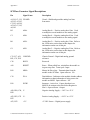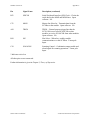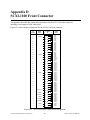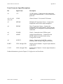
1
SCXI-1100
User Manual
32-Channel Differential Multiplexer/Amplifier Module for Signal Conditioning
October 1994 Edition
Part Number 320637C-01
© Copyright 1991, 1994 National Instruments Corporation.
All Rights Reserved.
National Instruments Corporate Headquarters
6504 Bridge Point Parkway
Austin, TX 78730-5039
(512) 794-0100
Technical support fax: (800) 328-2203
(512) 794-5678
Branch Offices:
Australia (03) 879 9422, Austria (0662) 435986, Belgium 02/757.00.20, Canada (Ontario) (519) 622-9310,
Canada (Québec) (514) 694-8521, Denmark 45 76 26 00, Finland (90) 527 2321, France (1) 48 14 24 24,
Germany 089/741 31 30, Italy 02/48301892, Japan (03) 3788-1921, Mexico 95 800 010 0793,
Netherlands 03480-33466, Norway 32-84 84 00, Singapore 2265886, Spain (91) 640 0085, Sweden 08-730 49 70,
Switzerland 056/20 51 51, Taiwan 02 377 1200, U.K. 0635 523545
Limited Warranty
The SCXI-1100 is warranted against defects in materials and workmanship for a period of one year from the date of
shipment, as evidenced by receipts or other documentation. National Instruments will, at its option, repair or replace
equipment that proves to be defective during the warranty period. This warranty includes parts and labor.
A Return Material Authorization (RMA) number must be obtained from the factory and clearly marked on the
outside of the package before any equipment will be accepted for warranty work. National Instruments will pay the
shipping costs of returning to the owner parts which are covered by warranty.
National Instruments believes that the information in this manual is accurate. The document has been carefully
reviewed for technical accuracy. In the event that technical or typographical errors exist, National Instruments
reserves the right to make changes to subsequent editions of this document without prior notice to holders of this
edition. The reader should consult National Instruments if errors are suspected. In no event shall National
Instruments be liable for any damages arising out of or related to this document or the information contained in it.
EXCEPT AS SPECIFIED HEREIN, N ATIONAL INSTRUMENTS MAKES NO WARRANTIES, EXPRESS OR IMPLIED,
AND SPECIFICALLY DISCLAIMS ANY WARRANTY OF MERCHANTABILITY OR FITNESS FOR A PARTICULAR
PURPOSE . CUSTOMER'S RIGHT TO RECOVER DAMAGES CAUSED BY FAULT OR NEGLIGENCE ON THE PART
OF NATIONAL INSTRUMENTS SHALL BE LIMITED TO THE AMOUNT THERETOFORE PAID BY THE CUSTOMER.
NATIONAL INSTRUMENTS WILL NOT BE LIABLE FOR DAMAGES RESULTING FROM LOSS OF DATA, PROFITS,
USE OF PRODUCTS, OR INCIDENTAL OR CONSEQUENTIAL DAMAGES, EVEN IF ADVISED OF THE POSSIBILITY
THEREOF. This limitation of the liability of National Instruments will apply regardless of the form of action,
whether in contract or tort, including negligence. Any action against National Instruments must be brought within
one year after the cause of action accrues. National Instruments shall not be liable for any delay in performance due
to causes beyond its reasonable control. The warranty provided herein does not cover damages, defects,
malfunctions, or service failures caused by owner's failure to follow the National Instruments installation, operation,
or maintenance instructions; owner's modification of the product; owner's abuse, misuse, or negligent acts; and
power failure or surges, fire, flood, accident, actions of third parties, or other events outside reasonable control.
Copyright
Under the copyright laws, this publication may not be reproduced or transmitted in any form, electronic or
mechanical, including photocopying, recording, storing in an information retrieval system, or translating, in whole or
in part, without the prior written consent of National Instruments Corporation.
Trademarks
LabVIEW ®, NI-DAQ ®, and RTSI ® are trademarks of National Instruments Corporation.
Product and company names listed are trademarks or trade names of their respective companies.
WARNING REGARDING MEDICAL AND CLINICAL USE
OF NATIONAL INSTRUMENTS PRODUCTS
National Instruments products are not designed with components and testing intended to ensure a level of reliability
suitable for use in treatment and diagnosis of humans. Applications of National Instruments products involving
medical or clinical treatment can create a potential for accidental injury caused by product failure, or by errors on the
part of the user or application designer. Any use or application of National Instruments products for or involving
medical or clinical treatment must be performed by properly trained and qualified medical personnel, and all
traditional medical safeguards, equipment, and procedures that are appropriate in the particular situation to prevent
serious injury or death should always continue to be used when National Instruments products are being used.
National Instruments products are NOT intended to be a substitute for any form of established process, procedure, or
equipment used to monitor or safeguard human health and safety in medical or clinical treatment.
Contents
About This Manual ........................................................................................................... xi
Organization of This Manual ....................................................................................... xi
Conventions Used in This Manual ............................................................................... xii
Related Documentation ................................................................................................ xiii
Customer Communication ........................................................................................... xiii
Chapter 1
Introduction ........................................................................................................................ 1-1
What Your Kit Should Contain.................................................................................... 1-1
Optional Software ........................................................................................................ 1-2
Optional Equipment ..................................................................................................... 1-3
Custom Cables ................................................................................................. 1-4
Unpacking .................................................................................................................... 1-4
Chapter 2
Configuration and Installation ..................................................................................... 2-1
Module Configuration .................................................................................................. 2-1
Digital Signal Connections .............................................................................. 2-3
Jumper W5 ........................................................................................... 2-3
Jumper W9 ........................................................................................... 2-4
Using Jumpers W5 and W9 ................................................................. 2-4
Jumper W11 (Revision A and B Modules Only) ................................. 2-4
Analog Configuration ...................................................................................... 2-5
Grounding, Shielding, and Output Mode Selection ............................. 2-6
Jumper W10 ............................................................................. 2-6
Reference Mode Selection ................................................................... 2-7
Jumper W1 ............................................................................... 2-7
Filter Selection ..................................................................................... 2-7
Jumpers W2 through W4 ......................................................... 2-7
Output Selection................................................................................... 2-8
Jumpers W7 and W8 ................................................................ 2-8
Input Filtering and Current Loop Receivers ........................................ 2-9
Hardware Installation ................................................................................................... 2-10
Signal Connections ...................................................................................................... 2-11
Front Connector ............................................................................................... 2-11
Front Connector Signal Descriptions ............................................................... 2-13
Analog Input Channels......................................................................... 2-13
Thermocouple Connections ................................................................. 2-16
Open Thermocouple Detection ............................................................ 2-17
Analog Output ...................................................................................... 2-17
Connector-and-Shell Assembly ........................................................... 2-17
SCXI-1300 Terminal Block ................................................................. 2-19
Terminal Block Temperature Sensor ....................................... 2-19
Terminal Block Jumper Configuration .................................... 2-19
Terminal Block Signal Connection .......................................... 2-20
Terminal Block Installation .................................................... 2-20
Rear Signal Connector ..................................................................................... 2-22
Rear Signal Connector Signal Descriptions ......................................... 2-23
© National Instruments Corporation
v
SCXI-1100 User Manual
Contents
Analog Output Signal Connections...................................................... 2-24
Digital I/O Signal Connections ............................................................ 2-24
Timing Requirements and Communication Protocol........................... 2-26
Timing Signal........................................................................... 2-26
Communication Signals ....................................................................... 2-26
Chapter 3
Theory of Operation ........................................................................................................ 3-1
Functional Overview .................................................................................................... 3-1
SCXIbus Connector ......................................................................................... 3-3
SCXIbus Connector Signal Descriptions ......................................................... 3-5
Digital Interface Circuitry ............................................................................................ 3-7
Digital Control Circuitry .............................................................................................. 3-8
Analog and Timing Circuitry ....................................................................................... 3-9
Analog Input and Timing Circuits ................................................................... 3-9
Calibration............................................................................................ 3-12
Analog Output Circuitry .................................................................................. 3-13
Scanning Modes ........................................................................................................... 3-14
Single-Module Multiplexed Scanning ............................................................. 3-14
Single-Module Multiplexed Scanning (Direct).................................... 3-14
Single-Module Multiplexed Scanning (Indirect) ................................. 3-15
Multiple-Module Multiplexed Scanning.......................................................... 3-15
Multiple-Chassis Scanning .............................................................................. 3-16
Chapter 4
Register Descriptions ....................................................................................................... 4-1
Register Description..................................................................................................... 4-1
Register Description Format ............................................................................ 4-1
SCXI-1100 Register Descriptions.................................................................... 4-1
Module ID Register.............................................................................. 4-2
Configuration Register ......................................................................... 4-3
Slot 0 Register Descriptions............................................................................. 4-6
Slot-Select Register .............................................................................. 4-7
Hardscan Control Register (HSCR) ..................................................... 4-8
FIFO Register....................................................................................... 4-9
Chapter 5
Programming ...................................................................................................................... 5-1
Programming Considerations....................................................................................... 5-1
Notation............................................................................................................ 5-1
Register Writes................................................................................................. 5-1
Register Selection and Write Procedure .............................................. 5-2
Initialization ......................................................................................... 5-3
Single-Channel Measurements ........................................................................ 5-3
Direct Measurements ........................................................................... 5-3
Indirect Measurements ......................................................................... 5-4
Measurements from Other Modules ........................................ 5-4
Measurements from the SCXI-1100 via Another Module ....... 5-4
Scanning Measurements .................................................................................. 5-5
1. Data Acquisition Board Setup Programming.................................. 5-6
Counter 1 and SCANDIV ........................................................ 5-7
2. Module Programming ..................................................................... 5-8
Single-Module Multiplexed Scanning (Direct)........................ 5-8
SCXI-1100 User Manual
vi
© National Instruments Corporation
Contents
Single-Module Multiplexed Scanning (Indirect) ..................... 5-8
Channel Scanning from Other Modules....................... 5-8
Channel Scanning from the SCXI-1100 via
Another Module ........................................................... 5-8
Multiple-Module Multiplexed Scanning.................................. 5-9
Multiple-Chassis Scanning ...................................................... 5-9
3. Programming the Slot 0 Hardscan Circuitry ................................... 5-10
4. Acquisition Enable, Triggering, and Servicing............................... 5-11
Scanning Examples ...................................................................................................... 5-11
Example 1 ........................................................................................................ 5-11
Example 2 ........................................................................................................ 5-12
Example 3 ........................................................................................................ 5-13
Appendix A
Specifications ...................................................................................................................... A-1
Analog Input ................................................................................................................ A-1
Explanation of Analog Input Specifications .................................................... A-2
Physical ........................................................................................................................ A-3
Cold-Junction Sensor ................................................................................................... A-3
Operating Environment ................................................................................................ A-3
Storage Environment.................................................................................................... A-3
Appendix B
Rear Signal Connector .................................................................................................... B-1
Rear Signal Connector Signal Descriptions ................................................................. B-2
Appendix C
SCXIbus Connector ......................................................................................................... C-1
SCXIbus Connector Signal Descriptions ..................................................................... C-3
Appendix D
SCXI-1100 Front Connector ......................................................................................... D-1
Front Connector Signal Descriptions ........................................................................... D-2
Appendix E
SCXI-1100 Cabling ........................................................................................................... E-1
SCXI-1340 Cable Assembly ........................................................................................ E-1
SCXI-1340 Installation .................................................................................... E-2
SCXI-1341 Lab-NB, Lab-PC, or Lab-PC+ and SCXI-1344 Lab-LC
Cable Assemblies ......................................................................................................... E-3
SCXI-1341 and SCXI-1344 Installation .......................................................... E-4
SCXI-1342 PC-LPM-16 Cable Assembly ................................................................... E-5
SCXI-1342 Installation .................................................................................... E-6
AT-MIO-16D and AT-MIO-64F-5 Board Connection................................................ E-6
SCXI-1351 and NB5 Cable Installation........................................................... E-6
SCXI-1180 Feedthrough Panel .................................................................................... E-8
SCXI-1180 Installation .................................................................................... E-8
SCXI-1302 50-Pin Terminal Block ............................................................................. E-10
SCXI-1302 Wiring Procedure.......................................................................... E-10
SCXI-1302 Installation .................................................................................... E-11
SCXI-1351 One-Slot Cable Extender .......................................................................... E-12
SCXI-1351 Installation .................................................................................... E-12
© National Instruments Corporation
vii
SCXI-1100 User Manual
Contents
SCXI-1350 Multichassis Adapter ................................................................................ E-12
SCXI-1350 Installation .................................................................................... E-13
SCXI-1343 Rear Screw Terminal Adapter .................................................................. E-13
SCXI-1343 Installation .................................................................................... E-13
Appendix F
Revision A and B Photo and Parts Locator Diagram ...........................................F-1
Appendix G
Customer Communication ............................................................................................. G-1
Glossary .....................................................................................................................Glossary-1
Index ................................................................................................................................ Index-1
SCXI-1100 User Manual
viii
© National Instruments Corporation
Contents
Figures
Figure
Figure
Figure
Figure
Figure
Figure
Figure
Figure
Figure
Figure
Figure
Figure
Figure
2-1.
2-2.
2-3.
2-4.
2-5.
2-6.
2-7.
2-8.
2-9.
2-10.
2-11.
2-12.
2-13.
SCXI-1100 Parts Locator Diagram .................................................................. 2-2
SCXI-1100 Front Connector Pin Assignment ................................................. 2-12
Ground-Referenced Signal Connection ........................................................... 2-14
Floating Signal Connection.............................................................................. 2-14
AC-Coupled Signal Connection....................................................................... 2-15
Assembling and Mounting the Connector-and-Shell Assembly ...................... 2-18
SCXI-1300 Parts Locator Diagram .................................................................. 2-21
SCXI-1100 Rear Signal Connector Pin Assignment ....................................... 2-22
SCANCLK Timing Requirements ................................................................... 2-26
Slot-Select Timing Diagram ............................................................................ 2-27
Serial Data Timing Diagram ............................................................................ 2-28
Configuration Register Write Timing Diagram ............................................... 2-29
SCXI-1100 Module ID Register Timing Diagram .......................................... 2-29
Figure
Figure
Figure
Figure
Figure
Figure
Figure
Figure
Figure
Figure
Figure
Figure
3-1.
3-2.
3-3.
3-4.
3-5.
3-6.
3-7.
3-8.
3-9.
3-10.
3-11.
3-12.
SCXI-1100 Block Diagram.............................................................................. 3-1
SCXI-1100 Detailed Block Diagram ............................................................... 3-2
SCXIbus Connector Pin Assignment ............................................................... 3-4
Digital Interface Circuitry Block Diagram ...................................................... 3-7
SCXI-1100 Digital Control Circuitry .............................................................. 3-8
Analog Input and Timing Block Diagram ....................................................... 3-10
Pad Locations ................................................................................................... 3-12
Analog Output Circuitry .................................................................................. 3-13
Single-Module Multiplexed Scanning (Direct)................................................ 3-15
Single-Module Multiplexed Scanning (Indirect) ............................................. 3-15
Multiple-Module Multiplexed Scanning.......................................................... 3-16
Multiple-Chassis Scanning .............................................................................. 3-16
Figure B-1.
SCXI-1100 Rear Signal Connector Pin Assignment ....................................... B-1
Figure C-1.
SCXIbus Connector Pin Assignment ............................................................... C-2
Figure D-1.
SCXI-1100 Front Connector Pin Assignment ................................................. D-1
Figure
Figure
Figure
Figure
Figure
SCXI-1340 Installation .................................................................................... E-3
NB5 Cable and SCXI-1351 Installation........................................................... E-7
SCXI-1180 Rear Connections.......................................................................... E-9
SCXI-1180 Front Panel Installation................................................................. E-10
Cover Removal ................................................................................................ E-11
E-1.
E-2.
E-3.
E-4.
E-5.
Figure F-1.
Figure F-2.
Revision A and B SCXI-1100 Signal Conditioning Module ........................... F-1
Revision A and B SCXI-1100 Parts Locator Diagram .................................... F-2
© National Instruments Corporation
ix
SCXI-1100 User Manual
Contents
Tables
Table
Table
Table
Table
Table
Table
Table
Table
Table
2-1.
2-2.
2-3.
2-4.
2-5.
2-6.
2-7.
2-8.
2-9.
Digital Signal Connections, Jumper Settings................................................... 2-5
Jumper W10 Settings ....................................................................................... 2-6
Jumper W1 Settings ......................................................................................... 2-7
Jumpers W2, W3, and W4 Settings ................................................................. 2-8
Jumpers W7 and W8 Settings .......................................................................... 2-9
User-Defined Input Filter Capacitors............................................................... 2-9
User-Defined Current Receiver Resistors ........................................................ 2-10
Jumper Setting on the Terminal Block ............................................................ 2-20
SCXIbus to SCXI-1100 Rear Signal Connector to Data Acquisition
Board Pin Equivalences ................................................................................... 2-25
Table 3-1.
Table 3-2.
SCXIbus Equivalents for the Rear Signal Connector ...................................... 3-6
Multiplexer/Input Channel Correspondence .................................................... 3-11
Table 5-1.
SCXI-1100 Rear Signal Connector Pin Equivalences ..................................... 5-2
Table
Table
Table
Table
SCXI-1100 and MIO Board Pinout Equivalences ........................................... E-2
SCXI-1341 and SCXI-1344 Pin Translations .................................................. E-4
SCXI-1342 Pin Translations ............................................................................ E-5
SCXI-1343 Pin Connections ............................................................................ E-14
E-1.
E-2.
E-3.
E-4.
SCXI-1100 User Manual
x
© National Instruments Corporation
About This Manual
This manual describes the electrical and mechanical aspects of the SCXI-1100 module and
contains information concerning its operation and programming. The SCXI-1100 operates as a
32-channel differential input multiplexer with an onboard software-programmable gain
instrumentation amplifier (PGIA). The SCXI-1100 is a member of the National Instruments
Signal Conditioning eXtensions for Instrumentation (SCXI) Series modules for the National
Instruments data acquisition plug-in boards. This module is designed for low-cost signal
conditioning of thermocouples, volt sources, millivolt sources, and 4 to 20 mA sources or 0 to
20 mA process-current sources.
This manual describes the installation, theory of operation, and basic programming
considerations for the SCXI-1100.
Organization of This Manual
The SCXI-1100 User Manual is organized as follows:
•
Chapter 1, Introduction, describes the SCXI-1100; lists the contents of your SCXI-1100 kit;
describes the optional software, optional equipment, and custom cables; and explains how to
unpack the SCXI-1100 kit.
•
Chapter 2, Configuration and Installation, describes the SCXI-1100 jumper configurations,
installation of the SCXI-1100 into the SCXI chassis, signal connections to the SCXI-1100,
and cable wiring.
•
Chapter 3, Theory of Operation, contains a functional overview of the SCXI-1100 module
and explains the operation of each functional unit making up the SCXI-1100.
•
Chapter 4, Register Descriptions, describes in detail the SCXI-1100 Module ID Register, the
Configuration Register, the Slot 0 registers, and multiplexer addressing.
•
Chapter 5, Programming, contains a functional programming description of the SCXI-1100
and Slot 0.
•
Appendix A, Specifications, lists the specifications for the SCXI-1100.
•
Appendix B, Rear Signal Connector, describes the pinout and signal names for the
SCXI-1100 50-pin rear signal connector, including a description of each connection.
•
Appendix C, SCXIbus Connector, describes the pinout and signal names for the SCXI-1100
96-pin SCXIbus connector, including a description of each connection.
•
Appendix D, SCXI-1100 Front Connector, describes the pinout and signal names for the
SCXI-1100 front connector, including a description of each connection.
•
Appendix E, SCXI-1100 Cabling, describes how to use and install the hardware accessories
for the SCXI-1100.
© National Instruments Corporation
xi
SCXI-1100 User Manual
About This Manual
•
Appendix F, Revision A and B Photo and Parts Locator Diagram, contains a photograph of
the Revision A and B SCXI-1100 and the parts locator diagram.
•
Appendix G, Customer Communication, contains forms you can use to request help from
National Instruments or to comment on our products and manuals.
•
The Glossary contains an alphabetical list and description of terms used in this manual,
including abbreviations, acronyms, metric prefixes, mnemonics, and symbols.
•
The Index contains an alphabetical list of key terms and topics in this manual, including the
page where you can find each one.
Conventions Used in This Manual
The following conventions are used in this manual.
italic
Italic text denotes emphasis, a cross reference, or an introduction to a key
concept.
Lab board
Lab board refers to the Lab-LC, Lab-NB, Lab-PC, and Lab-PC+ boards
unless otherwise noted.
MC
MC refers to the Micro Channel series computers.
MIO board
MIO board refers to the AT-MIO-16, AT-MIO-16D, AT-MIO-16F-5,
AT-MIO-16X, AT-MIO-64F-5, MC-MIO-16, NB-MIO-16, and
NB-MIO-16X multichannel I/O data acquisition boards unless otherwise
noted.
monospace
Lowercase text in this font denotes text or characters that are to be literally
input from the keyboard, sections of code, programming examples, and
syntax examples. This font is also used for the proper names of disk
drives, paths, directories, programs, subprograms, subroutines, device
names, functions, variables, filenames, and extensions, and for statements
and comments taken from program code.
NB
NB refers to the NuBus series computers.
PC
PC refers to the IBM PC/XT, the IBM PC AT, and compatible computers.
SCXIbus
SCXIbus refers to the backplane in the chassis. A signal on the backplane
is referred to as the SCXIbus <signal name> line (or signal). The
SCXIbus descriptor may be omitted when the meaning is clear.
Descriptions of all SCXIbus signals are given in Appendix C, SCXIbus
Connector.
Slot 0
Slot 0 refers to the power supply and control circuitry in the SCXI chassis.
Abbreviations, acronyms, metric prefixes, mnemonics, symbols, and terms are listed in the
Glossary.
SCXI-1100 User Manual
xii
© National Instruments Corporation
About This Manual
Related Documentation
The following documents contain information that you may find helpful as you read this manual:
•
AT-MIO-16 User Manual (part number 320476-01)
•
AT-MIO-16D User Manual (part number 320489-01)
•
AT-MIO-16F-5 User Manual (part number 320266-01)
•
AT-MIO-16X User Manual (part number 320488-01)
•
AT-MIO-64F-5 User Manual (part number 320487-01)
•
Lab-LC User Manual (part number 320380-01)
•
Lab-NB User Manual (part number 320174-01)
•
Lab-PC User Manual (part number 320205-01)
•
Lab-PC+ User Manual (part number 320502-01)
•
MC-MIO-16 User Manual, Revisions A to C (part number 320130-01)
•
MC-MIO-16 User Manual, Revision D (part number 320560-01)
•
NB-MIO-16 User Manual (part number 320295-01)
•
NB-MIO-16X User Manual (part number 320157-01)
•
PC-LPM-16 User Manual (part number 320287-01)
•
SCXI-1000/1001 User Manual (part number 320423-01)
Customer Communication
National Instruments wants to receive your comments on our products and manuals. We are
interested in the applications you develop with our products, and we want to help if you have
problems with them. To make it easy for you to contact us, this manual contains comment and
configuration forms for you to complete. These forms are in Appendix G, Customer
Communication, at the end of this manual.
© National Instruments Corporation
xiii
SCXI-1100 User Manual
Chapter 1
Introduction
This chapter describes the SCXI-1100; lists the contents of your SCXI-1100 kit; describes the
optional software, optional equipment, and custom cables; and explains how to unpack the
SCXI-1100 kit.
The SCXI-1100 module operates as a fast 32-channel differential multiplexer with an onboard
programmable gain instrumentation amplifier (PGIA). The SCXI-1100 is a module for signal
conditioning of thermocouples, volt sources, millivolt sources, 4 to 20 mA current sources, and
0 to 20 mA process-current sources. If you provide external excitation, you can also measure
thermistors, strain gauges, and RTDs.
The SCXI-1100 operates with full functionality with the National Instruments MIO boards. You
can use the Lab-LC, Lab-NB, Lab-PC, Lab-PC+, and PC-LPM-16 boards with the SCXI-1100,
but these boards can perform only single-channel reads and cannot scan the module. You can
also use the SCXI-1100 with other systems that comply with the specifications given in
Chapter 2, Configuration and Installation. Each SCXI-1100 module multiplexes its 32 input
channels into a single channel of the data acquisition board. You can multiplex several
SCXI-1100s into a single channel, thus greatly increasing the number of analog input signals that
you can digitize.
An additional shielded terminal block has screw terminals for easy signal attachment to the
SCXI-1100. In addition, a temperature sensor for cold-junction compensation of thermocouples
is included on the terminal block. This cold-junction reference (CJR) is either multiplexed with
the 32 channels or jumper connected to a different channel of the data acquisition board.
With the SCXI-1100 module, the SCXI chassis can serve as a fast-scanning signal conditioner
for laboratory testing, production testing, and industrial-process monitoring.
What Your Kit Should Contain
The contents of the SCXI-1100 kit (part number 776572-00) are listed as follows.
Kit Component
Part Number
SCXI-1100 module
SCXI-1100 User Manual
181690-01
320637-01
If your kit is missing any of the components, contact National Instruments.
© National Instruments Corporation
1-1
SCXI-1100 User Manual
Introduction
Chapter 1
Optional Software
This manual contains complete instructions for directly programming the SCXI-1100. You can
order separate software packages for controlling the SCXI-1100 from National Instruments.
When you use the SCXI-1100 in combination with the PC, AT, or MC data acquisition boards
with the SCXI-1100, you can use LabVIEW for Windows or LabWindows ® for DOS.
LabVIEW and LabWindows are innovative program development software packages for data
acquisition and control applications. LabVIEW uses graphical programming, whereas
LabWindows enhances Microsoft C and QuickBASIC. Both packages include extensive
libraries for data acquisition, instrument control, data analysis, and graphical data presentation.
You can use the SCXI-1100, together with the NB Series data acquisition boards, with
LabVIEW for Macintosh, a software system that features interactive graphics, a state-of-the-art
user interface, and a powerful graphical programming language. The LabVIEW Data
Acquisition Virtual Instrument (VI) Library, a series of VIs for using LabVIEW with National
Instruments boards, is included with LabVIEW. The LabVIEW Data Acquisition VI Library is
functionally equivalent to the NI-DAQ software for Macintosh.
The NI-DAQ driver software is shipped free with National Instruments data acquisition boards.
NI-DAQ has a library of functions that you can call from your application programming
environment. These functions include routines for analog input (A/D conversion), buffered data
acquisition (high-speed A/D conversion), analog output (D/A conversion), waveform generation,
digital I/O, counter/timer, SCXI, Real-Time System Integration (RTSI), and self-calibration.
NI-DAQ maintains a consistent software interface among its different versions so you can switch
between platforms with minimal modifications to your code.
The National Instruments PC, AT, and MC data acquisition boards are packaged with NI-DAQ
software for DOS/Windows/LabWindows. NI-DAQ software for DOS/Windows/LabWindows
comes with language interfaces for Professional BASIC, Turbo Pascal, Turbo C, Turbo C++,
Borland C++, and Microsoft C for DOS; and Visual Basic, Turbo Pascal, Microsoft C with SDK,
and Borland C++ for Windows. NI-DAQ software for DOS/Windows/LabWindows is on highdensity 5.25 in. and 3.5 in. diskettes. You can use your SCXI-1100, together with your PC, AT,
and MC Series data acquisition boards, with NI-DAQ software for DOS/Windows/LabWindows.
The National Instruments NB Series data acquisition boards are packaged with NI-DAQ software
for Macintosh. NI-DAQ software for Macintosh comes with language interfaces for MPW C,
THINK C, Pascal, and Microsoft QuickBASIC. Any language that uses Device Manager
Toolbox calls can access NI-DAQ software for Macintosh. You can use your SCXI-1100,
together with the NB Series data acquisition boards, with NI-DAQ software for Macintosh.
SCXI-1100 User Manual
1-2
© National Instruments Corporation
Chapter 1
Introduction
Optional Equipment
Equipment
Part Number
SCXI-1300 front terminal block
SCXI-1310 96-pin connector and shell
SCXI-1340 cable assembly
SCXI-1341 Lab-NB/Lab-PC/Lab-PC+ cable assembly
SCXI-1342 PC-LPM-16 cable assembly
SCXI-1343 screw terminal adapter
SCXI-1344 Lab-LC cable assembly
SCXI-1345 shielded cable
1m
2m
5m
10 m
SCXI-1346 shielded multichassis cable adapter
SCXI-1347 SCXI shielded cable assembly
with 1 m cable
with 2 m cable
with 5 m cable
with 10 m cable
SCXI-1349 SCXI shielded cable assembly
with 1 m cable
with 2 m cable
with 5 m cable
with 10 m cable
SCXI-1350 multichassis adapter
SCXI-1351 one-slot cable extender
SCXI process-current resistor kit
Standard ribbon cable
0.5 m
1.0 m
NB5 cable
0.5 m
1.0 m
NB6 cable
0.5 m
1.0 m
776573-00
776573-10
776574-40
776574-41
776574-42
776574-43
776574-44
776574-451
776574-452
776574-455
776574-450
776574-46
776574-471
776574-472
776574-475
776574-470
776574-491
776574-492
776574-495
776574-490
776575-50
776575-51
776582-01
180524-05
180524-10
181304-05
181304-10
181305-01
181305-10
Refer to the Signal Connections section in Chapter 2, Configuration and Installation, and to
Appendix E, SCXI-1100 Cabling, for additional information on cabling, connectors, and
adapters.
© National Instruments Corporation
1-3
SCXI-1100 User Manual
Introduction
Chapter 1
Custom Cables
The SCXI-1100 rear signal connector is a 50-pin male ribbon-cable header. The manufacturer
part number of the header National Instruments uses is as follows:
• AMP Inc. (part number 1-103310-0)
The mating connector for the SCXI-1100 rear signal connector is a 50-position polarized ribbonsocket connector with strain relief. National Instruments uses a polarized or keyed connector to
prevent inadvertent upside-down connection to the SCXI-1100. Recommended manufacturer
part numbers for this mating connector are as follows:
• Electronic Products Division/3M (part number 3425-7650)
• T&B/Ansley Corporation (part number 609-5041CE)
Part numbers of standard 50-conductor 28 AWG stranded-ribbon cables that you can use with
these connectors are as follows:
• Electronic Products Division/3M (part number 3365/50)
• T&B/Ansley Corporation (part number 171-50)
The SCXI-1100 front connector is a 96-pin DIN C male connector. The manufacturer part
number of this connector National Instruments uses is as follows:
• Harting Electronik Inc. (part number 09-03-396-6921)
The mating connector for the SCXI-1100 front connector is a 96-pin DIN C female connector.
National Instruments uses a polarized connector to prevent inadvertent upside-down connection
to the SCXI-1100. Recommended manufacturer part numbers for this mating connector are as
follows:
• AMP Inc. (part number 535020-1; right-angle pins)
• Panduit Corporation (part number 100-096-434; straight-solder eyelet pins)
Unpacking
Your SCXI-1100 module is shipped in an antistatic package to prevent electrostatic damage to
the module. Several components on the module can be damaged by electrostatic discharge. To
avoid such damage in handling the module, take the following precautions:
•
Touch the antistatic package to a metal part of your SCXI chassis before removing the
module from the package.
•
Remove the module from the package and inspect the module for loose components or any
other sign of damage. Notify National Instruments if the module appears damaged in any
way. Do not install a damaged module into your SCXI chassis.
SCXI-1100 User Manual
1-4
© National Instruments Corporation
Chapter 2
Configuration and Installation
This chapter describes the SCXI-1100 jumper configurations, installation of the SCXI-1100 into
the SCXI chassis, signal connections to the SCXI-1100, and cable wiring.
Module Configuration
Revision C and later SCXI-1100 modules contain 10 jumpers that are shown in the parts locator
diagram in Figure 2-1. For the Revision A and B parts locator diagram, see Appendix F,
Revision A and B Photo and Parts Locator Diagram.
© National Instruments Corporation
2-1
SCXI-1100 User Manual
Chapter 2
Configuration and Installation
The jumpers are used as follows:
•
•
Fixed jumpers
-
Jumper W6 is reserved; do not remove this jumper.
-
On Revision A and B modules, jumper W9 is unused; do not connect this jumper.
-
On Revision C and later modules, jumper W11 does not exist. On Revision A and B
modules, jumper W11 carries the SLOT0SEL* signal from the rear signal connector,
after buffering, to the SCXIbus INTR* line; leave this jumper in the factory-default
position (position A).
User-configurable jumpers
-
Jumper W5 carries the SCXIbus MISO line, after buffering, to the SERDATOUT signal
on the rear signal connector.
-
On Revision C and later modules, jumper W9 connects a pullup resistor to the
SERDATOUT signal on the rear signal connector.
-
Jumper W10 configures the guard, the analog output ground, and enables the
Pseudodifferential Output mode.
-
Jumpers W7 and W8 connect the module output to the front connector.
-
Jumper W1 provides a DC path for the bias current of the PGIA when used with floating
or AC-coupled sources.
-
Jumpers W2 through W4 are used to set the lowpass filter (LPF) or full
bandwidth (FBW).
Further configuration of the board is software controlled and is discussed later in this chapter.
Digital Signal Connections
The SCXI-1100 has two jumpers (three jumpers on Revision A and B modules) dedicated for
communication between the data acquisition board and the SCXIbus backplane/Slot 0. These
jumpers are W5 and W9 (and W11 on Revision A and B modules). In most cases, you do not
need to move these jumpers. See Table 2-1 later in this chapter for the description and
configuration of the jumper settings.
Jumper W5
Position 1 connects, after buffering, the SCXIbus MISO line to the SERDATOUT pin of the rear
signal connector. This is the factory-default setting. In this setting, along with the proper setting
of jumper W9, the data acquisition board can read the Module ID Register of the SCXI-1100.
See the Timing Requirements and Communication Protocol section later in this chapter, and
Chapter 4, Register Descriptions, for information on reading the Module ID Register. See
Appendix E, SCXI-1100 Cabling, for the pin equivalences of the SCXI-1100 rear signal
connector and the data acquisition board I/O connector. This position is marked on the module.
© National Instruments Corporation
2-3
SCXI-1100 User Manual
Configuration and Installation
Chapter 2
Position 3 disconnects SERDATOUT from the SCXIbus MISO line.
Jumper W9
On Revision C and later modules, position 1 connects a 2.2 kΩ pullup resistor to the
SERDATOUT line. Position 3 does not connect the pullup resistor to the SERDATOUT line.
On Revision A and B modules, do not connect jumper W9.
Using Jumpers W5 and W9
If the SCXI-1100 is not cabled to a data acquisition board, the positions of these jumpers do not
matter, so leave them in their factory-default positions (both in position 1).
If the SCXI-1100 is cabled to a data acquisition board, and the SCXI chassis that the SCXI-1100
is in, is the only SCXI chassis cabled to that data acquisition board, leave the jumpers in their
factory-default positions (both in position 1).
If the SCXI-1100 is cabled to a data acquisition board, and there are multiple SCXI chassis
cabled to that data acquisition board with shielded cables (you are using SCXI-1346 shielded
cable multichassis adapters), leave the jumpers in their factory-default positions (both in position
1).
If the SCXI-1100 is cabled to a data acquisition board, and there are multiple SCXI chassis
cabled to that data acquisition board with ribbon cables (you are using SCXI-1350 multichassis
adapters), leave jumper W5 in its factory-default position (position 1). On all but one of the
SCXI-1100s that are cabled to the data acquisition board, move jumper W9 to position 3. It does
not matter which of the SCXI-1100 modules that are cabled to the data acquisition board has
jumper W9 set to position 1. If you have different types of modules cabled to the data
acquisition board, those different modules will have jumpers similar to W5 and W9 of the SCXI
1100. Set those jumpers on the different modules using the same method described here for the
SCXI-1100.
On Revision A and B SCXI-1100s, jumper W9 is not used. You set jumper W5 as explained in
the cases above, except in the case of a multiple chassis ribbon-cable system. In a multichassis
ribbon-cable system with Revision A and B SCXI-1100s cabled to the data acquisition board,
you can access the MISO line in only one chassis. Pick one of the chassis that has the
SCXI-1100 cabled to the data acquisition board. Set jumper W5 on the SCXI-1100 to position 1.
On the SCXI-1100s that are in the other chassis and cabled to the data acquisition board, set
jumper W5 to position 3. Notice that you will only be able to access digital information from the
chassis that has the SCXI-1100 with jumper W5 set to position 1.
Jumper W11 (Revision A and B Modules Only)
On Revision C and later modules, jumper W11 does not exist. SLOT0SEL* is always buffered
to the INTR* line.
On Revision A and B modules, position A connects, after buffering, SLOT0SEL* to the
SCXIbus INTR* line. Do not change the factory setting, position A. In this setting, the data
SCXI-1100 User Manual
2-4
© National Instruments Corporation
Chapter 2
Configuration and Installation
acquisition board controls the SCXIbus INTR* line. See the Timing Requirements and
Communication Protocol section later in this chapter, and Chapter 5, Programming, for
information on the use of the INTR* line. See Appendix E, SCXI-1100 Cabling, for the pin
equivalences of the SCXI-1100 rear signal connector and the data acquisition board I/O
connector.
Do not use position B, which is reserved.
Table 2-1. Digital Signal Connections, Jumper Settings
Jumper
W9
W9
W11
Factory setting; do not remove this
jumper
Connects pullup to SERDATOUT
(Revision C and higher modules only);
factory-default setting
Parking position (not connected on
Revision A and B modules)
Factory default (Revision A and B
modules only)
•
2
•
3
•
1
•
2
•
3
•
•
W6
Parking position
1
•
W5
Connects MISO to SERDATOUT;
factory-default setting
Configuration
•
W5
Description
3
2
1
1
•
2
•
3
•
1
•
2
•
3
•
A
B
•
•
•
Analog Configuration
The SCXI-1100 has seven analog configuration jumpers–W10, W7, W8, W1, W2, W3, and W4.
Use these jumpers to configure the output mode, reference mode, filter selection, and amplifier
output selection.
© National Instruments Corporation
2-5
SCXI-1100 User Manual
Configuration and Installation
Chapter 2
Grounding, Shielding, and Output Mode Selection
Jumper W10
Position A-R0R1 is the parking position and the factory setting.
Position AB-R0 connects the PGIA reference to the analog output ground (pins 1 and 2 on the
rear signal connector).
Position AB-R1 connects the PGIA reference to the SCXIbus guard.
Position AB-R2 enables the Pseudodifferential Output mode and connects the PGIA reference to
the OUTREF pin on the rear signal connector. Select this mode when the SCXI-1100 has to
operate with data acquisition boards that have a nonreferenced single-ended input (NRSE). Do
not use differential input data acquisition boards when jumper W10 is in the AB-R2 position.
Table 2-2. Jumper W10 Settings
•
B
•
•
A
B
•
R2
A
B
•
R1
•
R0
•
R1
•
R0
•
•
R2
•
R1
•
R0
•
•
•
•
•
A
•
R2
R2
•
Enables the Pseudodifferential Output
mode (connects pin 19 of the PGIA
output reference to the rear signal
connector)
R1
•
W10
Connects the PGIA reference to the
SCXIbus guard
R0
B
•
W10
Connects the data acquisition analog
ground (pins 1 and 2 on the rear signal
connector) to the PGIA reference (used
with single-ended boards)
A
•
W10
Factory setting; parking position (used
with MIO boards in differential mode)
Configuration
•
W10
Description
•
Jumper
When using the SCXI-1100 with data acquisition boards such as the MIO boards, use the
Differential Input mode configuration to eliminate ground problems. With single-ended data
SCXI-1100 User Manual
2-6
© National Instruments Corporation
Chapter 2
Configuration and Installation
acquisition boards, such as the Lab boards and the PC-LPM-16, place jumper W10 in position
AB-R0 to connect the data acquisition board ground reference to the module analog ground
reference.
Reference Mode Selection
Jumper W1
Jumper W1 references the negative (-) input of the PGIA to ground through a 100 kΩ resistor.
The SCXI-1100 is shipped with jumper W1 in the parking position. Use this setting when
connecting to signals that are referenced to ground.
If you are measuring floating sources, you can move jumper W1 to position 3 to reference the
negative (-) input of the PGIA to ground through the 100 kΩ resistor. Refer to Figures 2-3, 2-4,
and 2-5 later in this chapter for signal connection diagrams.
Note:
If all of the sources are floating, you can configure jumper W1 to connect a 100 kΩ
resistor to the negative input of the amplifier to prevent saturation of the amplifier
inputs. This reduces the input impedance, however, and usually increases settling time
and common-mode noise. Also, if any of the sources are ground-referenced or have
high leakage to ground, a ground loop can result, causing DC offsets or noise.
Therefore, it is best if you do not use this jumper but instead connect your floating
channels to the chassis ground on the terminal block via a wire.
Table 2-3. Jumper W1 Settings
Jumper
Factory setting; parking position (used
for ground-referenced sources)
Configuration
•
•
•
W1
Description
1
Floating source connection
3
•
•
•
W1
2
1
2
3
For more information on input signal connections, see the Signal Connections section later in this
chapter.
Filter Selection
Jumpers W2 through W4
One jumper block is provided for jumpers W2, W3, and W4:
•
When you connect jumper W2, the SCXI-1100 does not filter.
•
When you connect jumper W3, a 10 kHz lowpass filter filters the conditioned signal.
•
When you connect jumper W4, a 4 Hz lowpass filter filters the conditioned signal.
© National Instruments Corporation
2-7
SCXI-1100 User Manual
Configuration and Installation
Chapter 2
Table 2-4. Jumpers W2, W3, and W4 Settings
Jumper
W2
Description
Factory setting is full bandwidth
(FBW) and no filtering
Configuration
•
•
•
•
•
•
W2 W3 W4
W3
10 kHz lowpass filter
•
•
•
•
•
•
W2 W3 W4
W4
4 Hz lowpass filter
•
•
•
•
•
•
W2 W3 W4
Note: The settling time varies greatly when you configure the SCXI-1100 to a 4 Hz or 10 kHz
filter or full bandwidth. Refer to Appendix A, Specifications, for details on how fast you
can scan in each case.
Output Selection
Jumpers W7 and W8
Position A connects the module output channel MCH0 to the front connector. Position B
disconnects the front connector from the module output. Use this setting if you do not need the
amplifier output at the front connector. Refer to the Analog Output section later in this chapter
for more information.
SCXI-1100 User Manual
2-8
© National Instruments Corporation
Chapter 2
Configuration and Installation
Table 2-5. Jumpers W7 and W8 Settings
Configuration
Amplifier Reference is connected to
the front connector AOREF pin
•
W8
A
•
B
•
Amplifier Output is connected to the
front connector OUTPUT pin
B
A
B
•
W7
•
Factory setting; parking position
•
W8
•
A
•
Factory setting; parking position.
Disconnects the front connector from
the module output
B
•
W7
•
A
•
Description
•
Jumper
Input Filtering and Current Loop Receivers
If you need input filtering, pads in which you can insert a capacitor are available at each input
channel. Table 2-6 shows which capacitor reference designator corresponds to which input
channel.
Table 2-6. User-Defined Input Filter Capacitors
Input Channel
Spare Capacitor Reference
Designator
0
1
2
3
4 through 7
8 through 11
12 through 15
16 through 19
20 through 23
24 through 27
28 through 31
C1
C5
C4
C2
C10 through C7 respectively
C16 through C13 respectively
C22 through C19 respectively
C30 through C27 respectively
C38 through C35 respectively
C44 through C41 respectively
C50 through C47 respectively
In addition, pads are available for transforming individual channels to current-to-voltage
converters. National Instruments manufactures an SCXI process-current pack, which consists of
a package of four 249 Ω, 0.1%, 5 ppm/°C, 1/4 W resistors. The part number for this kit is in the
Optional Equipment section of Chapter 1, Introduction. Table 2-7 shows the input channels and
their corresponding resistor reference designators.
© National Instruments Corporation
2-9
SCXI-1100 User Manual
Configuration and Installation
Chapter 2
Table 2-7. User-Defined Current Receiver Resistors
Input Channel
Resistor Reference Designator
0 through 3
4 through 7
8 through 11
12 through 15
16 through 19
20 through 23
24 through 27
28 through 31
R5 through R2 respectively
R9 through R6 respectively
R13 through R10 respectively
R17 through R14 respectively
R21 through R18 respectively
R25 through R22 respectively
R29 through R26 respectively
R33 through R30 respectively
For more information, refer to the Analog Input and Timing Circuits section in Chapter 3, Theory
of Operation.
To install either the capacitors or the resistors, perform the following steps before installing your
module in the SCXI chassis:
1.
Take off the module cover by removing the grounding screw at the rear of the module.
2.
Take off the rear panel by removing the two other screws.
3.
Slide the module out of its enclosure.
4.
Insert the capacitor(s) and/or resistor(s) into their appropriate pads.
5.
Solder the leads to the pads on the solder side of the board.
6.
Trim the leads to 0.06 in. maximum.
7.
Slide the module back into its enclosure.
8.
Reinstall the rear panel.
9.
Reinstall the top cover and grounding screw.
Your module is ready to be installed into the chassis.
Hardware Installation
You can install the SCXI-1100 in any available SCXI chassis. After you have made any
necessary changes and have verified and recorded the jumper settings (a form is included in
Appendix G, Customer Communication), you are ready to install the SCXI-1100. The following
are general installation instructions. Consult your SCXI chassis user manual for specific
instructions and warnings.
1. Turn off the computer that contains the data acquisition board or disconnect the data
acquisition board from your SCXI chassis.
2. Turn off the SCXI chassis. Do not insert the SCXI-1100 into a chassis that is turned on.
SCXI-1100 User Manual
2-10
© National Instruments Corporation
Chapter 2
Configuration and Installation
3. Insert the SCXI-1100 into the board guides. Gently guide the module into the back of the
slot until the connectors make good contact. If you have already installed a cable assembly
in the rear of the chassis, you must firmly engage the module and cable assembly; however,
do not force the module into place.
4. Screw the front mounting panel of the SCXI-1100 to the top and bottom threaded strips of
your SCXI chassis.
5. If you will connect this module to any MIO data acquisition board except the AT-MIO-16D
and the AT-MIO-64F-5, attach the connector at the metal end of an SCXI-1340 cable
assembly to the rear signal connector on the SCXI-1100 module. Screw the rear panel to the
rear threaded strip. Attach the loose end of the cable to the MIO board.
Note: If you already have another module in your chassis that is cabled to your data
acquisition board, you generally do not need to connect additional cabling to the
SCXI-1100. Typically, only one module in a chassis is cabled to a data acquisition
board.
For installation procedures with other SCXI accessories and data acquisition boards, consult
Appendix E, SCXI-1100 Cabling.
6. Check the installation.
7. Turn on the SCXI chassis.
8. Turn on the computer or reconnect the data acquisition board to your chassis.
The SCXI-1100 module is installed and ready for operation.
Signal Connections
This section describes the input and output signal connections to the SCXI-1100 board via the
SCXI-1100 front connector and rear signal connector, and includes specifications and connection
instructions for the signals given on the SCXI-1100 connectors.
Warning: Connections to any terminal that exceed any of the maximum ratings of input or
output signals on the SCXI-1100 can damage the SCXI-1100 module and the
SCXIbus backplane. Maximum input ratings for each signal are given in this chapter
under the discussion of that signal. National Instruments is not liable for any
damages resulting from signal connections that exceed these ratings.
Front Connector
Figure 2-2 shows the pin assignments for the SCXI-1100 front connector.
© National Instruments Corporation
2-11
SCXI-1100 User Manual
Configuration and Installation
Chapter 2
Pin
Number
32
Signal
Name
A
Column
B
C
CH0CH0+
CH1CH1+
CH2CH2+
CH3CH3+
CH4CH4+
CH5CH5+
CH6CH6+
CH7CH7+
CH8CH8+
CH9CH9+
CH10CH10+
CH11CH1+
CH12CH12+
CH13CH13+
CH14CH14+
CH15CH15+
CH16CH16+
CH17CH17+
CH18CH18+
CH19CH19+
CH20CH20+
CH21CH21+
CH22CH22+
CH23CH23+
CH24CH24+
CH25CH25+
CH26CH26+
CH27CH27+
CH28CH28+
CH29CH29+
CH30CH30+
CH31CH31+
CGND
31
30
29
28
27
26
25
24
CGND
23
22
21
20
19
18
17
16
CGND
15
14
13
12
11
10
9
8
OUTPUT
7
AOREF
6
GUARD
5
CGND
4
DTEMP
3
MTEMP
2
CGND
1
+5 V
Signal
Name
Figure 2-2. SCXI-1100 Front Connector Pin Assignment
SCXI-1100 User Manual
2-12
© National Instruments Corporation
Chapter 2
Configuration and Installation
Front Connector Signal Descriptions
Pin
Signal Name
Description
A1
+5 V
+5 VDC Source – Used to power the temperature
sensor on the terminal block. 0.2 mA of source not
protected.
A2, A5, A16,
A24, A32
CGND
Chassis Ground – Tied to the SCXI chassis.
A3
MTEMP
Multiplexed Temperature Sensor – Connects the
temperature sensor to the output multiplexer.
A4
DTEMP
Direct Temperature Sensor – Connects the
temperature sensor to the MCH1+ signal when the
terminal block is configured for direct temperature
connection.
A6
GUARD
Guard – Connected to the SCXIbus guard.
A7
AOREF
Analog Output Reference – Connected to the
MCH0- signal as described in the Analog
Configuration section.
A8
OUTPUT
Output – Connected to the MCH0+ signal as
described in the Analog Configuration section.
B1-B32
CH31- through CH0-
Negative Input Channels – Negative input channels
to the PGIA.
C1-C32
CH31+ through CH0+
Positive Input Channels – Positive input channels to
the PGIA.
The signals on the front connector are all analog but can be divided into three groups–the analog
input channels, the temperature sensor, and the analog output channel.
Analog Input Channels
Columns B and C constitute the analog input channels for the multiplexed PGIA inputs. The
inputs are configured in Differential mode, hence you should ground reference the measured
signal if it is floating. If the measured signals are floating, connect jumper W1 (position 2-3) to
produce a DC path for the input bias currents; otherwise, the PGIA bias currents charge up stray
capacitances, resulting in uncontrollable drift and possible saturation. Figure 2-3 illustrates how
to connect a ground-referenced signal. Figure 2-4 illustrates how to connect a floating signal.
Figure 2-5 shows how to connect AC-coupled signals.
© National Instruments Corporation
2-13
SCXI-1100 User Manual
Configuration and Installation
Chapter 2
+
PGIA
–
+
VS
W1
–
+
Vcm
–
+
Vout
–
(Position 1-2)
•
•
•
•
•
•
•
•
•
100 kΩ
Figure 2-3. Ground-Referenced Signal Connection
+
PGIA
–
+
VS
W1
(Position 2-3)
–
•
•
•
•
•
•
•
•
•
+
Vout
–
100 kΩ
Figure 2-4. Floating Signal Connection
SCXI-1100 User Manual
2-14
© National Instruments Corporation
Chapter 2
Configuration and Installation
+
PGIA
–
+
VS
W1
(Position 2-3)
–
+
Vout
–
100 kΩ
100 kΩ
Figure 2-5. AC-Coupled Signal Connection
For AC-coupled signals, connect jumper W1 and an external resistor from the positive input
channel to the chassis ground. This connection produces the DC path for the positive input bias
current. Typical resistor values range from 100 kΩ to 1 MΩ. Although this configuration is
necessary in this case, it lowers the input impedance of the PGIA and introduces an additional
offset voltage proportional to the input offset current and to the resistor value used. The typical
input offset current of the PGIA consists of ±350 pA and a negligible offset drift current. A
100 kΩ resistor results in ±35 µV of offset, which is insignificant in most applications.
However, if you use larger valued bias resistors, significant input offset may result. To determine
the maximum offset introduced by the biasing resistor, use the following equation:
V ofsbias = I ofsbias ( R bias ) + ( R bias − 100 kΩ )I bias
Use a 100 kΩ value when you use jumper W1 to reduce the amount of offset as well as to
maintain a balanced input and avoid the degradation of the PGIA common-mode rejection ratio
(CMRR). If you need larger valued biasing resistors, do not use jumper W1, and tie an external
biasing resistor to the negative input channels.
For DC-coupled signals, connect jumper W1; no external resistors are required. This
configuration internally connects a 100 kΩ value from the negative input of the PGIA to ground,
producing the required biasing. This configuration does not affect the input offset or the
differential input impedance because the voltage developing across the bias resistor appears as a
common-mode voltage.
The SCXI-1100 PGIA can reject any voltage within its common-mode input range that ground
potential differences between the signal source and the module introduce. In addition, the PGIA
can reject common-mode noise pickup in the leads connecting the signal sources to the
SCXI-1100.
The common-mode input range of the SCXI-1100 PGIA is the magnitude of the greatest
common-mode signal that the SCXI-1100 can reject. The PGIA can reject common-mode
© National Instruments Corporation
2-15
SCXI-1100 User Manual
Configuration and Installation
Chapter 2
signals in which both the positive and negative channel inputs are in the ±10 V range. Thus the
common-mode input range for the SCXI-1100 depends on the size of the differential input signal:
Vdiff = V+in - V-in
The exact formula for the permissible common-mode input range is as follows:
Vc = ± ( 10 V - G1 ( V+in - V-in )/2)
Thus, with a differential voltage of 10 V and a first-stage gain of G1 = 1, the maximum possible
common-mode voltage would be ±5 V. You measure the actual common-mode voltage available
at the PGIA input with respect to the SCXI-1100 ground. You can calculate the actual
common-mode voltage with the following formula:
Vcm-actual = (V+in + V-in )/2
where V+in is the signal at the positive input channel (CH#+) and V-in is the signal at the
negative input channel (CH#-). Both V+in and V-in are measured with respect to the SCXI-1100
chassis ground.
The analog input channels are overvoltage protected to ±25 VDC with power on and to ±15 VDC
with power off at a maximum of 20 mA sink or source.
Warning: Exceeding the differential and common-mode input ranges results in distorted input
signals. Exceeding the maximum input voltage rating between any two terminals
can damage the SCXI-1100, the SCXIbus backplane, and the data acquisition board.
National Instruments is not liable for any damages resulting from such signal
connections.
Thermocouple Connections
One of the main applications of the SCXI-1100 is thermocouple measurements. This section
describes the different type of thermocouple connections.
Your thermocouple can be either floating or ground referenced. When you connect your
thermocouple, make sure you know whether the thermocouple is floating or ground referenced.
If you are using a floating thermocouple, you must ground the PGIA CH- in one of the following
two ways:
•
Connect a wire on the terminal block from the CH- of interest to the chassis ground screw
terminal. If you are using several similar thermocouples, you can daisy chain the CH- of
interest to the chassis ground screw terminal. Use this method to avoid grounding all the
SCXI-1100 CH- and to create a solid ground connection; this is the recommended method of
referencing floating thermocouples.
•
Internally connect jumper W1 to the floating source position. This will connect all
SCXI-1100 CH- inputs to ground via a 100 kΩ resistor. However, this setting usually
increases settling time and common-mode noise.
If you are using a grounded thermocouple, do not ground the SCXI-1100 CH- and do not use
jumper W1 to ground floating signals because you will create a ground loop and adversely affect
the accuracy of your measurement.
SCXI-1100 User Manual
2-16
© National Instruments Corporation
Chapter 2
Configuration and Installation
Open Thermocouple Detection
For the SCXI-1100 to be able to detect open thermocouples, you must properly connect your
signals as explained in the previous section.
When the thermocouple opens, the PGIA bias currents charge the internal parasitic capacitors,
driving the PGIA inputs and output to saturation. Because it is not possible to predict the
direction of the bias currents, the PGIA can saturate to either the positive or negative rail. This is
open thermocouple detection.
Because the PGIA has low bias currents, the charging of the stray capacitances, and therefore
saturation, can be a slow process. It is best to have a self-test scan to check for open
thermocouples. Perform this self-test scan with the SCXI-1100 gain set to a minimum of 100
and the scan at a maximum rate of 15 Hz when you are in full bandwidth or in the 10 kHz filter,
and 3.5 Hz when you are in the 4 Hz filter. You can then execute this scan at regular intervals to
verify that all the thermocouples are connected. Saturation or a positive or negative reading
outside the expected range indicates an open thermocouple.
Analog Output
You can connect MCH0+ and MCH0- to the front connector to pins A8 and A7, respectively, via
internal jumpers as described in the Output Selection section earlier in this chapter. When you
do not need the module output at the front connector, place jumpers W7 and W8 in position B,
thus connecting pins A8 and A7 of the front connector to the module analog ground. This
connection reduces the amount of noise and stray capacitance coupling from the amplifier output
to its inputs, improving the settling time performance. In addition to the analog output, pin A6
connects to the SCXIbus guard.
Connector-and-Shell Assembly
Two types of signal connectors are available to connect the signals to the SCXI-1100. The first,
the SCXI-1310 96-pin connector-and-shell assembly, is available in a kit listed in the Optional
Equipment section in Chapter 1, Introduction. The connector has eyelet ends for easy hook-andsolder wire connection. With this kit, you can build your own signal cable to connect to the
SCXI-1100 inputs. After you have built the cable, use the shell to cover and protect the
connector.
Perform the following steps to build and mount the connector-and-shell assembly to your SCXI
module:
1. Refer to Figure 2-6 and the diagram included with your SCXI-1310 kit to build the
connector-and-shell assembly.
2. Turn off the computer that contains your plug-in board or disconnect the board from your
SCXI chassis.
3. Turn off your SCXI chassis.
4. Slide the module out of the chassis.
5. Remove the module cover. Refer to Figure 2-6 as you complete the remaining steps.
6. Place one jack screw as indicated in Figure 2-6.
© National Instruments Corporation
2-17
SCXI-1100 User Manual
Configuration and Installation
Chapter 2
7. While holding the jack screw in place, insert the lock washer and then the nut. Notice that
you might need long-nose pliers to insert the washer and nut.
8. Tighten the nut by holding it firmly and rotating the jack screw.
9. Repeat steps 6 through 8 for the second jack screw.
10. Replace the module cover and tighten the grounding screw.
11. Slide the module back into place in the chassis.
12. Connect the connector-and-shell assembly to your module front connector and secure the
assembly by tightening both mounting screws.
Shell Assembly
Mounting Screw
Connector
Jack
Screws
SCXI-1100 Module
Lock Washers
Nut
Nut
Shell Assembly
Grounding Screw
Mounting Screw
Figure 2-6. Assembling and Mounting the Connector-and-Shell Assembly
SCXI-1100 User Manual
2-18
© National Instruments Corporation
Chapter 2
Configuration and Installation
SCXI-1300 Terminal Block
The second type of connector available to connect the signals to the SCXI-1100 inputs is the
SCXI-1300 terminal block, which consists of a shielded board with 72 screw terminals to
connect to the SCXI-1100 input connector. Thirty-two pairs of screw terminals are for signal
connection to the 32 differential inputs of the SCXI-1100. One pair of screw terminals connects
to the chassis ground. Three screw terminals connect to the SCXI-1100 OUTPUT and AOREF
pins and to the SCXIbus guard. The remaining three screw terminals are not used. In addition,
solder pads are on each side of the terminal block for circuit additions.
Terminal Block Temperature Sensor
The temperature sensor is located on the SCXI-1300 terminal block. You can connect the
temperature sensor in two ways:
•
Multiplexed Temperature Sensor (MTS) mode–Connect the temperature sensor to the
MTEMP pin (A3) on the front connector and multiplex the sensor at the output multiplexer
along with the PGIA output.
•
Direct Temperature Sensor (DTS) mode–Connect the temperature sensor to a separate data
acquisition channel via MCH1± (pins 5 and 6 on the rear signal connector).
The temperature sensor outputs 10 mV/°C and has an accuracy of ±0.9° C over the 0° to 55° C
temperature range. To determine the temperature, use the following formulas:
(
T(°C) = 100 V TEMPOUT
T(° F) =
)
[T(°C)] 9 + 32
5
where VTEMPOUT is the temperature sensor output and T(°F) and T(°C) are the temperature
readings in degrees Fahrenheit and degrees Celsius, respectively.
Terminal Block Jumper Configuration
The SCXI-1100 has two jumpers for configuring the onboard temperature sensor. Jumper W1
(MTEMP) connects the temperature sensor output to the SCXI-1100 output multiplexer. This is
the factory setting. Jumper W2 (DTEMP) connects the temperature sensor to the SCXI-1100
MCH1+ signal on the rear signal connector.
In both MTS and DTS modes, the reference to the temperature sensor signal is the SCXI-1100
analog ground that is connected to MCH0- in the MTS mode and to MCH1- in the DTS mode.
Notice that MCH1- is continuously connected to the SCXI-1100 ground, whereas MCH0- is
switched through the output multiplexer.
One jumper block comprises both jumpers; thus, you can use only one type of configuration at a
time. The parking position for the jumper block is in the MTEMP position. The temperature
sensor is disabled until the RTEMP bit in the Configuration Register selects the sensor.
Table 2-8 shows the SCXI-1300 jumper settings.
© National Instruments Corporation
2-19
SCXI-1100 User Manual
Configuration and Installation
Chapter 2
Table 2-8. Jumper Setting on the Terminal Block
Jumper
Description
MTS mode selected; factory
setting; parking position
•
•
W1
Position
MTEMP
•
•
W2
DTEMP
DTS mode selected
•
•
W1
MTEMP
•
•
W2
DTEMP
Terminal Block Signal Connection
To connect the signal to the terminal block, you will need Phillips-head number 1 and number 2
screwdrivers and a 0.125 in. flathead screwdriver. Use the following procedure (refer to the
SCXI-1300 terminal block parts locator diagram in Figure 2-7):
1. Remove the grounding screw of the top cover with the Phillips-head number 1 screwdriver.
2. Snap out the top cover of the shield by placing the flathead screwdriver in the groove at the
bottom of the terminal block.
3. After loosening the strain-relief screws screws with the Phillips-head number 2 screwdriver,
slide the signal wires one at a time through the front panel strain-relief opening. Add
insulation or padding if necessary.
4. Connect the wires to the screw terminals by inserting the wires into the terminals and
tightening the screw without letting the wires slip out of the strain-relief bar.
5. Tighten the larger strain-relief screws.
6. Snap the top cover back into place.
7. Reinsert the grounding screw to ensure proper shielding.
8. Connect the terminal block to the SCXI-1100 front connector as explained in the Terminal
Block Installation section, the next section in this chapter.
Terminal Block Installation
To connect the terminal block to the SCXI-1100 front connector, perform the following steps:
1. Connect the SCXI-1100 front connector to its mating connector on the terminal block.
2. Make sure that the SCXI-1100 top and bottom thumbscrews do not obstruct the rear panel of
the terminal block.
3. Tighten the top and bottom screws on the back of the terminal block to hold it securely in
place.
SCXI-1100 User Manual
2-20
© National Instruments Corporation
Configuration and Installation
Chapter 2
Rear Signal Connector
Note: If you will be using the SCXI-1100 with a National Instruments data acquisition board
and cable assembly, you do not need to read the remainder of this chapter. If you will
also be using the SCXI-1180 feedthrough panel, the SCXI-1343 rear screw terminal
adapter, or the SCXI-1351 one-slot cable extender with the SCXI-1100, you should read
this section.
Figure 2-8 shows the pin assignments for the SCXI-1100 rear signal connector.
AOGND
1
2
AOGND
MCH0+
3
4
MCH0-
MCH1+
5
6
MCH1-
7
8
9
10
11 12
13 14
15 16
17 18
OUTREF
19 20
21 22
23 24
DIG GND
SERDATIN
25 26
SERDATOUT
DAQD*/A
27 28
SLOT0SEL*
29 30
31 32
DIG GND
33 34
35 36
SERCLK
SCANCLK
37 38
39 40
41 42
RSVD
43 44
45 46
47 48
49 50
Figure 2-8. SCXI-1100 Rear Signal Connector Pin Assignment
SCXI-1100 User Manual
2-22
© National Instruments Corporation
Chapter 2
Configuration and Installation
Rear Signal Connector Signal Descriptions
Pin
Signal Name
Description
1-2
AOGND
Analog Output Ground – Connected to the PGIA
reference when jumper W10 is in position AB-R0.
3-6
MCH0± and MCH1±
Analog Output Channels 0 and 1 – Connects to the
data acquisition differential analog input channels.
19
OUTREF
Output Reference – Serves as the reference node for
the PGIA output in the Pseudodifferential Output
mode. You should connect OUTREF to the analog
input sense of the NRSE data acquisition board.
24, 33
DIG GND
Digital Ground – Supply the reference for data
acquisition digital signals and are tied to the module
digital ground.
25
SERDATIN
Serial Data In – Taps into the SCXIbus MOSI line
to provide serial input data to a module or Slot 0.
26
SERDATOUT
Serial Data Out – Taps into the SCXIbus MISO line
to accept serial output data from a module.
27
DAQD*/A
Data Acquisition Board Data/Address Line – Taps
into the SCXIbus D*/A line to indicate to the
module whether the incoming serial stream is data
or address information.
29
SLOT0SEL*
Slot 0 Select – Taps into the SCXIbus INTR* line
to indicate whether the information on MOSI is
being sent to a module or Slot 0.
36
SCANCLK
Scan Clock – Indicates to the SCXI-1100 that the
data acquisition board has taken a sample; also
causes the SCXI-1100 to change channels.
37
SERCLK
Serial Clock – Taps into the SCXIbus SPICLK line
to clock the data on the MOSI and MISO lines.
43
RSVD
Reserved.
* Indicates active low.
All other pins are not connected.
See the Timing Requirements and Communication Protocol section later in this chapter for more
detailed information on timing.
The signals on the rear signal connector are analog output signals, digital I/O signals, or timing
I/O signals. Signal connection guidelines for each of these groups are given in the following
section.
© National Instruments Corporation
2-23
SCXI-1100 User Manual
Configuration and Installation
Chapter 2
Analog Output Signal Connections
Pins 1 through 6 and pin 19 of the rear signal connector are analog output signal pins. Pins 1 and
2 are AOGND signal pins. AOGND is an analog output common signal that is routed through
jumper W10 to the PGIA reference on the SCXI-1100. You can use these pins for a general
analog power ground tie point to the SCXI-1100 if necessary. In particular, when using
differential input data acquisition boards, such as the MIO boards, it is preferable to leave
jumper W10 in its factory setting or in position AB-R1 to avoid ground loops. With data
acquisition boards that are configured for referenced single-ended (RSE) measurements, set
jumper W10 in position AB-R0 to connect the SCXI-1100 ground to the data acquisition analog
ground. Pin 19, the OUTREF pin, is connected internally to the PGIA reference when jumper
W10 is in position AB-R2. Pins 3 through 6 are the analog output channels of the SCXI-1100.
Pins 3 and 4, or MCH0±, are a multiplexed output of the PGIA output and the temperature sensor
output. Pins 5 and 6, or MCH1±, are a direct connection of the temperature sensor to the rear
signal connector. Notice that the temperature sensor is located on the terminal block. For further
details on configuring the temperature sensor output, refer to the SCXI-1300 Terminal Block
section earlier in this chapter.
Warning: The SCXI-1100 analog outputs are not overvoltage protected. Applying external
voltage to these outputs can damage the SCXI-1100. National Instruments is not
liable for any damages resulting from such signal connections.
Digital I/O Signal Connections
Pins 24 through 27, 29, 33, 36, 37, and 43 constitute the digital I/O lines of the rear signal
connector. These pins are divided into three categories–the digital input signals, the digital
output signals, and the digital timing signals.
The digital input signals are pins 24, 25, 27, 29, 33, and 37. The data acquisition board uses
these pins to configure the SCXI module when the module is under data acquisition board
control. Each digital line emulates the SCXIbus communication signals as follows:
•
Pin 25 is SERDATIN and is equivalent to the SCXIbus MOSI serial data input line.
•
Pin 27 is DAQD*/A and is equivalent to the SCXIbus D*/A line. Pin 27 indicates to the
module whether the incoming serial stream on SERDATIN is data (DAQD*/A = 0), or
address (DAQD*/A = 1) information.
•
Pin 29 is SLOT0SEL* and is equivalent to the SCXIbus INTR* line. Pin 29 indicates
whether the data on the SERDATIN line is being sent to Slot 0 (SLOT0SEL* = 0) or to a
module (SLOT0SEL* = 1).
•
Pins 24 and 33 are the digital ground references for the data acquisition board digital signals
and are tied to the module digital ground.
•
Pin 37, SERCLK, is equivalent to the SCXIbus SPICLK line and clocks the serial data on the
SERDATIN line into the module registers.
The digital output signal is pin 26:
•
Pin 26 is SERDATOUT and is equivalent to the SCXIbus MISO line when jumper W5 is in
position 3.
SCXI-1100 User Manual
2-24
© National Instruments Corporation
Chapter 2
Configuration and Installation
The digital I/O signals of the SCXI-1100 match the digital I/O lines of the MIO board. When
used with an SCXI-1341, SCXI-1342, or SCXI-1344 cable assembly, the SCXI-1100 signals
match the digital lines of the Lab-NB/Lab-PC/Lab-PC+, PC-LPM-16, and Lab-LC boards,
respectively. Table 2-9 lists the equivalences. For more information, consult Appendix E,
SCXI-1100 Cabling.
Table 2-9. SCXIbus to SCXI-1100 Rear Signal Connector to
Data Acquisition Board Pin Equivalences
SCXIbus Line
SCXI-1100
Rear Signal
Connector
MIO Board
Lab-LC/Lab-NB/
Lab-PC/Lab-PC+
PC-LPM-16
MOSI
D*/A
INTR*
SPICLK
MISO
SERDATIN
DAQD*/A
SLOT0SEL*
SERCLK
SERDATOUT
ADIO0
ADIO1
ADIO2
EXTSTROBE*
BDIO0
PB4
PB5
PB6
PB7
PC1
DOUT4
DOUT5
DOUT6
DOUT7
DIN6
The digital timing signals are pins 36 and 43:
•
Pin 36 is a SCXI-1100 clock that increments the MUXCOUNTER after each data acquisition
board conversion during scanning. This signal is referred to as SCANCLK. See Chapter 3,
Theory of Operation, for a description of MUXCOUNTER.
•
Pin 43 is a reserved digital input.
The following specifications and ratings apply to the digital I/O lines:
Absolute maximum voltage
input rating
5.5 V with respect to DIG GND
Digital input specifications (referenced to DIG GND):
VIH input logic high voltage
VIL input logic low voltage
2 V minimum
0.8 V maximum
II input current leakage
±1 µA maximum
Digital output specifications (referenced to DIG GND):
VOH output logic high voltage
VOL output logic low voltage
© National Instruments Corporation
3.7 V minimum at 4 mA maximum
0.4 V maximum at 4 mA maximum
2-25
SCXI-1100 User Manual
Configuration and Installation
Chapter 2
Timing Requirements and Communication Protocol
Timing Signal
The data acquisition timing signal is SCANCLK.
SCANCLK increments MUXCOUNTER on its rising edge. Figure 2-9 shows the timing
requirements of the SCANCLK signal that ensure that SCANCLK is properly transmitted over
TRIG0.
SCANCLK
Tlow
Thigh
Thigh
Tlow
Time low before rising edge
Time high before falling edge
400 nsec minimum
250 nsec minimum
Figure 2-9. SCANCLK Timing Requirements
For settling time specifications, refer to Appendix A, Specifications.
Communication Signals
This section describes the methods for communicating on the Serial Peripheral Interface (SPI)
bus and their timing requirements. The communication signals are SERDATIN, DAQD*/A,
SLOT0SEL*, SERDATOUT, and SERCLK. Furthermore, Slot 0 produces SS* according to
data acquisition board programming, so this section also describes SS* timing relationships. For
more information on the Slot 0 Slot-Select Register, consult Chapter 4, Register Descriptions.
The data acquisition board writes a slot-select number to Slot 0 to determine to which slot the
board will talk. In the case of an SCXI-1001 chassis, this write also determines to which chassis
the data acquisition board will talk. Writing a slot-select number also programs the Slot 0
hardscan circuitry. See Chapter 5, Programming, for information on programming the Slot 0
hardscan circuitry.
Use the following procedure to select a slot in a particular chassis. Figure 2-10 illustrates the
timing of this procedure with the example case of selecting Slot 11 in Chassis 9. Notice that the
factory-default chassis address for the SCXI-1000 is address 0. For information on changing the
address of your chassis, consult the SCXI-1000/1001 User Manual. An SCXI-1000 chassis
responds to any chassis number.
SCXI-1100 User Manual
2-26
© National Instruments Corporation
Chapter 2
Configuration and Installation
SLOT0SEL*
SS*X
Chassis Y
SS*11
Chassis 9
Tss_dis
Tclk_wait
Tss_en
SERCLK
Tslot0sel*_wait
SERDATIN
0 1
0 0
1
1
Chassis ID = 9
Tss _ dis
Tclk _ wait
Tslot0sel* _ wait
Tss _ en
0
1
1
Slot 11
SLOT0SEL* low to SS* disabled
SLOT0SEL* low to first rising edge on SERCLK
Last rising edge on SERCLK to SLOT0SEL* high
SLOT0SEL* high to SS* enabled
200 nsec maximum
75 nsec minimum
250 nsec minimum
350 nsec maximum
Figure 2-10. Slot-Select Timing Diagram
To write the 16-bit slot-select number to Slot 0, perform the following steps:
1. Initial conditions:
SERDATIN = don't care.
DAQD*/A = don't care.
SLOT0SEL* = 1.
SERCLK = 1.
2. Clear SLOT0SEL* to 0. This deasserts all SS* lines to all modules in all chassis.
3. For each bit, starting with the MSB, perform the following actions:
a. Set SERDATIN = bit to be sent. These bits are the data that is being written to the
Slot-Select Register.
b. Clear SERCLK to 0.
c. Set SERCLK to 1. This rising edge clocks the data.
4. Set SLOT0SEL* to 1. This asserts the SS* line of the module whose slot number was
written to Slot 0. If you are using multiple chassis, only the appropriate slot in the chassis
whose address corresponds to the written chassis number is selected. When no
communication is taking place between the data acquisition board and any modules, write
zero to the Slot-Select Register to ensure that no accidental writes occur.
Figure 2-11 shows the timing requirements on the SERCLK and SERDATIN signals. You must
observe these timing requirements for all communications. T delay is a specification of the
SCXI-1100.
© National Instruments Corporation
2-27
SCXI-1100 User Manual
Configuration and Installation
Chapter 2
Thigh
Tlow
SERCLK
Tsetup
Thold
SERDATIN
Tdelay
SERDATOUT
Tlow
Thigh
Tsetup
Thold
Tdelay
Minimum low time
Minimum high time
SERDATIN setup time
SERDATIN hold time
SERDATOUT delay
65 nsec minimum
400 nsec minimum
200 nsec minimum
200 nsec minimum
350 nsec maximum
Figure 2-11. Serial Data Timing Diagram
After the Slot-Select line to an SCXI-1100 has been asserted, you can write to the module
Configuration Register and read from the Module ID Register using the following protocols.
Deassert Slot-Select to reinitialize the contents of the Module ID Register. After the 32 bits of
data are read from the Module ID Register, further data will be zeros until reinitialization occurs.
To write to the Configuration Register, perform the following steps:
1. Initial conditions:
SS* asserted low.
SERDATIN = don't care.
DAQD*/A = 0 (indicates data will be written to the Configuration Register).
SLOT0SEL* = 1.
SERCLK = 1 (and has not transitioned since SS* went low).
2. For each bit to be written:
Establish the desired SERDATIN level corresponding to this bit.
Clear SERCLK to 0.
Set SERCLK to 1. Clock the data.
3. Pull SLOT0SEL* low to deassert the SS* line and establish conditions for writing a new
slot-select number to the Slot 0 Slot-Select Register.
4. If you are not selecting another slot, write zero to the Slot 0 Slot-Select Register.
Figure 2-12 illustrates a write to the SCXI-1100 Configuration Register of the binary pattern:
00010010 10011111 00000111
SCXI-1100 User Manual
2-28
© National Instruments Corporation
Chapter 2
Configuration and Installation
SLOT0SEL*
SS*
SERCLK
SERDATIN
0 0 0 1 0 0 1 0 1 0 0 1 1 1 1 1 0 0 0 0 0 1 1 1
Figure 2-12. Configuration Register Write Timing Diagram
To read from the Module ID Register, perform the following steps:
1. Initial conditions:
SS* asserted low.
SERDATIN = don't care.
DAQD*/A = 1. Make sure DAQD*/A does not go low or erroneous data will be written
to the Configuration Register.
SLOT0SEL* = 1.
SERCLK = 1 (and has not changed since SS* went low).
2. For each bit to be read:
Clear SERCLK to 0.
Set SERCLK to 1. Clock the data.
Read the level of the SERDATOUT line.
3. Pull SLOT0SEL* low to deassert the SS* line and establish conditions for writing a new
slot-select number to the Slot 0 Slot-Select Register.
4. If you are not selecting another slot, you should write zero to the Slot 0 Slot-Select Register.
Figure 2-13 illustrates a read of the SCXI-1100 Module ID Register.
SLOT0SEL*
SS*
SERCLK
SERDATOUT
0 0 0 0 0 1 1 0 0 0 0 0 0 0 0 0 0 0 0 0 0 0 0 0 0 0 0 0 0 0 0 0
Tdelay
byte 0 = 6
Tdelay
byte 1 = 0
byte 2 = 0
SS* high to SERDATOUT high
byte 3 = 0
350 nsec maximum
Figure 2-13. SCXI-1100 Module ID Register Timing Diagram
For further details on programming these signals, refer to Chapter 5, Programming.
© National Instruments Corporation
2-29
SCXI-1100 User Manual
Chapter 3
Theory of Operation
This chapter contains a functional overview of the SCXI-1100 module and explains the operation
of each functional unit making up the SCXI-1100.
Functional Overview
The block diagram in Figure 3-1 illustrates the key functional components of the SCXI-1100.
Figure 3-2 shows the detailed block diagram.
Front Connector
Digital
Interface
and
Control
Analog
Input
and
Timing
Analog
Output
Stage
Rear Signal Connector
SCXIbus
Figure 3-1. SCXI-1100 Block Diagram
© National Instruments Corporation
3-1
SCXI-1100 User Manual
SCXI-1100 User Manual
3-2
DTEMP
MTEMP
CH31
MUX
Counter
Analog
MUXes
and Input
Protection
Gain Control
Auto Zero
and CAL
Switches
PGIA
Digital
Interface and Control
From Analog Bus 2
Low-Pass
Filter
Analog
Bus
Switch
Buffer
To Analog
Bus 0
Scan Clock
MCH1
MCH0
Rear Signal Connector
SCXIbus Connector
CH0
CH1
Theory of Operation
Chapter 3
Figure 3-2. SCXI-1100 Detailed Block Diagram
© National Instruments Corporation
Front Connector
Chapter 3
Theory of Operation
The major components of the SCXI-1100 are as follows:
•
The SCXIbus connector
•
The digital interface
•
The digital control circuitry
•
The timing and analog circuitry
The SCXI-1100 consists of eight CMOS four-to-one dual multiplexers for a total of 32
differential channels and a PGIA with gains of 1, 2, 5, 10, 20, 50, 100, 200, 500, 1,000, and
2,000. The SCXI-1100 also has a digital section for automatic control of channel scanning, gain
selection, amplifier output selection, MUXCOUNTER clock selection, calibration, and autozeroing.
The theory of operation for each of these components is explained in the remainder of this
chapter.
SCXIbus Connector
Figure 3-3 shows the pinout of the SCXIbus connector.
© National Instruments Corporation
3-3
SCXI-1100 User Manual
Theory of Operation
Chapter 3
GUARD
GUARD
GUARD
AB0+
GUARD
GUARD
GUARD
GUARD
GUARD
GUARD
AB2+
RESET*
MISO
VVCHSGND
CHSGND
V+
V+
+5 V
SPICLK
TRIG0
SS*
A1
B1
A2
B2
A3
B3
A4
B4
A5
B5
A6
B6
A7
B7
A8
B8
A9
B9
A10
B10
A11
B11
A12
B12
A13
B13
A14
B14
A15
B15
A16
B16
A17
B17
A18
B18
A19
B19
A20
B20
A21
B21
A22
B22
A23
B23
A24
B24
D1
C1
D2
C2
D3
C3
D4
C4
D5
C5
D6
C6
D7
C7
D8
C8
D9
C9
D10
C10
D11
C11
D12
C12
D13
C13
D14
C14
D15
C15
D16
C16
D17
C17
D18
C18
D19
C19
D20
C20
D21
C21
D22
C22
D23
C23
D24
C24
GUARD
GUARD
GUARD
AB0GUARD
GUARD
GUARD
GUARD
GUARD
GUARD
AB2-
CHSGND
CHSGND
CHSGND
CHSGND
CHSGND
RSVD
INTR*
D*/A
VVCHSGND
CHSGND
V+
V+
+5 V
MOSI
SCANCON
Figure 3-3. SCXIbus Connector Pin Assignment
SCXI-1100 User Manual
3-4
© National Instruments Corporation
Chapter 3
Theory of Operation
SCXIbus Connector Signal Descriptions
Pin
Signal Name
Description
A1, B1, C1, D1, GUARD
A2, D2, A3, B3,
C3, D3, A4, D4,
A5, B5, C5, D5,
A6, D6
Guard – Shield and guard the analog bus lines
from noise.
B2
AB0+
Analog Bus 0+ – Positive analog bus 0 line. Used
to multiplex several modules to one analog signal.
C2
AB0-
Analog Bus 0- – Negative analog bus 0 line. Used
to multiplex several modules to one analog signal.
B6
AB2+
Analog Bus 2+ – Positive analog bus 2 line. Refer to
the Calibration section later in this chapter for
information on the use of this pin.
C6
AB2-
Analog Bus 2- – Negative analog bus 2 line. Refer to
the Calibration section later in this chapter for
information on the use of this pin.
C13-C17, A21, CHSGND
B21, C21, D21
Chassis Ground – Digital and analog ground
reference.
C18
RSVD
Reserved.
A19
RESET*
Reset – When pulled low, reinitializes the module to
its power-up state. Totem pole. Input.
B19
MISO
Master-In-Slave-Out – Transmits data from the
module to the SCXIbus. Open collector. I/O.
C19
D*/A
Data/Address – Indicates to the module whether address
information or data information is being sent to the
module on MOSI. Open collector. I/O.
D19
INTR*
Interrupt – Active low. Causes data that is on
MOSI to be written to the Slot-Select Register in
Slot 0. Open collector. Output.
A20, B20, C20, VD20
Negative Analog Supply – -18.5 V to -25 V.
A22, B22, C22
D22
V+
Positive Analog Supply – +18.5 V to +25 V.
A23, D23
+5 V
+5 VDC Source – Digital power supply.
© National Instruments Corporation
3-5
SCXI-1100 User Manual
Theory of Operation
Chapter 3
Pin
Signal Name
Description (continued)
B23
SPICLK
Serial Peripheral Interface (SPI) Clock – Clocks the
serial data on the MOSI and MISO lines. Open
collector. I/O.
C23
MOSI
Master-Out-Slave-In – Transmits data from the
SCXIbus to the module. Open collector. I/O.
A24
TRIG0
TRIG0 – General-purpose trigger line that the
SCXI-1100 uses to send SCANCLK to other
modules or receive SCANCLK from other modules.
Open collector. I/O.
B24
SS*
Slot Select – When low, enables module
communications over the SCXIbus. Totem pole.
Input.
C24
SCANCON
Scanning Control – Combination output enable and
reload signal for scanning operations. Totem pole.
Input.
* Indicates active low
All other pins are not connected.
MOSI, MISO, SPICLK, and SS* form a synchronous communication link that conforms with
SPI using an idle-high clock and second-edge data latching. D*/A, INTR*, and RESET* are
additional control signals.
When the module is installed in an SCXI-1000 or SCXI-1001 chassis, the data acquisition board,
via the module rear signal connector, must tap into the open-collector backplane signal lines as a
master to write to the module. Table 3-1 shows the signal connections from the rear signal
connector to the backplane.
Table 3-1. SCXIbus Equivalents for the Rear Signal Connector
Rear Signal Connector
Signal
SCXIbus Equivalent
SERDATIN
DAQD*/A
SLOT0SEL*
MOSI
D*/A
INTR* You must set jumper W11 to position A
(Revision A and B modules only)
SPICLK
MISO You must set jumper W5 to position 3
SERCLK
SERDATOUT
The SCXI-1100 module converts the data acquisition board signals to open-collector signals on
the backplane of the SCXI chassis. For the data acquisition board to talk to a slot, the board must
first assert the SS* for that slot. This is done by asserting INTR* low, writing a 16-bit number
over MOSI corresponding to the desired slot (and chassis if you are using an SCXI-1001
SCXI-1100 User Manual
3-6
© National Instruments Corporation
Chapter 3
Theory of Operation
chassis), and then releasing INTR* high. At this point, the SS* of the desired slot is asserted low
and the data acquisition board can communicate with the module in that slot according to the SPI
protocol.
Digital Interface Circuitry
Figure 3-4 shows a diagram of the SCXI-1100 and SCXIbus digital interface circuitry.
SERDATIN
Buffered Serial
Data
DAQD*/A
Digital
Interface
Buffered Digital
Control Signals
SLOT0SEL*
SERCLK
Rear Signal Connector
SS*
MOSI
D*/A
INTR*
SPICLK
MISO
SCXIbus
SERDATOUT
Figure 3-4. Digital Interface Circuitry Block Diagram
The digital interface circuitry is divided into a data acquisition section and an SCXIbus section.
The SCXI-1100 connects to the SCXIbus via a 4x24 metral receptacle and to the data acquisition
board via a 50-pin ribbon-cable header.
© National Instruments Corporation
3-7
SCXI-1100 User Manual
Theory of Operation
Chapter 3
Digital Control Circuitry
Figure 3-5 diagrams the SCXI-1100 digital control circuitry.
Module ID Register
Serial Data Out
Buffered
Serial Data In
Input Channel
Select
Configuration
Register
Output
Stage
Control
PGIA
Gain
Select
Buffered Digital
Control Signals
SCANCLK
Path
Control
Hardware
Scan
Control
Figure 3-5. SCXI-1100 Digital Control Circuitry
The digital control circuitry section consists of the Configuration Register and the Module ID
Register.
The Configuration Register is a 3-byte serial-in parallel-out shift register. Data is received on the
MOSI line from either Slot 0 or the data acquisition board when SS* is enabled and D*/A
indicates data transfer (D*/A low). You use the Configuration Register for channel, gain,
calibration, and auto-zeroing selection, in addition to configuring the SCXI-1100 for scanning
options. All the control bits and the gain-select bits feed into a latch before being routed to the
rest of the module. The channel-select bits are taken directly from the shift register. Complete
descriptions of the register bits are given in Chapter 4, Register Descriptions. Writes to the
Configuration Register require the following steps:
1. Drive SS* low to enable communication with the board.
2. Drive D*/A low to indicate that the information sent on the MOSI line is data.
3. The serial data becomes available on MOSI. SPICLK clocks the data into the register.
4. Drive SS* high and D*/A high to indicate an end of communication. This latches the Configuration
Register bits.
SCXI-1100 User Manual
3-8
© National Instruments Corporation
Chapter 3
Theory of Operation
When you reset the SCXIbus, all bits in the Configuration Register clear.
The Module ID Register connects to MISO on the SCXIbus. The Module ID Register is an 8-bit
parallel/serial-in serial-out shift register and an SPI communication adapter. During the first four
bytes of transfer after SS* is asserted low, the contents of the Module ID Register are written
onto MISO. Zeros are written to MISO thereafter until SS* is released and reasserted. The
SCXI-1100 module ID is hex 00000006.
Analog and Timing Circuitry
The SCXIbus produces analog power (±18.5 VDC) that is regulated on the SCXI-1100 to
±15 VDC, a guard, analog buses (AB0±, AB2±) and a chassis ground (CHSGND). AB0± buses
the SCXI-1100 output to other modules or receives outputs from other modules via the SCXIbus.
The module can use AB2± to receive a precision voltage for auto calibration of the PGIA. Refer
to the Calibration section later in this chapter for more information. The guard guards both
analog buses. You can connect the guard via jumper W10 to the PGIA ground reference, or
leave the guard floating (another board can make a connection).
The data acquisition board analog input and timing is the interface between the SCXI-1100
output and the data acquisition board. This interface is described in the following section.
Analog Input and Timing Circuits
Figure 3-6 diagrams the SCXI-1100 analog input and timing circuitry.
© National Instruments Corporation
3-9
SCXI-1100 User Manual
Theory of Operation
Chapter 3
Timing Signals
Input Channel
Select
MUXCOUNTER
and
Channel Select
MUX0
and Input Protection
Calibration or
Input Selection
Calibration
and
Auto-Zero
Hardware
Auto-Zero or
Auto-Calibration
Selection
MUX1
and Input Protection
From AB2±
Gain Select
Front Connector
MUX2
and Input Protection
MUX3
and Input Protection
+
PGIA
MUX4
and Input Protection
To Output Multiplexer
–
MUX5
and Input Protection
MUX6
and Input Protection
MUX7
and Input Protection
Figure 3-6. Analog Input and Timing Block Diagram
The analog input and timing circuitry consists of an input multiplexer, channel select hardware, a
software-programmable gain instrumentation amplifier, and calibration hardware.
The input multiplexer consists of eight CMOS analog input multiplexers and has 32 differential
analog input channels. Input channels and multiplexers correspond as shown in Table 3-2.
SCXI-1100 User Manual
3-10
© National Instruments Corporation
Chapter 3
Theory of Operation
Table 3-2. Multiplexer/Input Channel Correspondence
Multiplexer
Input Channels
0
1
2
3
4
5
6
7
0 through 3
4 through 7
8 through 11
12 through 15
16 through 19
20 through 23
24 through 27
28 through 31
The analog input overvoltage protection is ±25 V when powered on and ±15 V when powered
off.
The channel-select hardware consists of a 5-bit counter, MUXCOUNTER, and a three-to-eight
decoder. The module sends to the decoder the three MSBs of the counter to determine which
multiplexer is addressed, and the two LSBs to determine which of the four channels of the
selected multiplexer is to be read. In the Single-Channel Read mode, the module loads the
MUXCOUNTER with the desired channel number. In the Scanning mode, the module loads the
counter with the first channel to be read. During the scan, the counter is clocked by SCANCLK
from the data acquisition board, or TRIG0 from the SCXIbus, depending on the state of the
CLKSELECT bit in the Configuration Register. During scanning operations, MUXCOUNTER
is reloaded with the channel value stored in the Configuration Register when SCANCON is high
(inactive) and counts upwards on each rising clock edge when SCANCON is low (active).
The instrumentation amplifier on the SCXI-1100 board fulfills two purposes. The PGIA
converts a differential input signal into a single-ended signal with respect to the SCXI-1100
ground for input common-mode signal rejection. With this conversion, the module can extract
the input analog signal from a common-mode voltage or noise before the data acquisition board
samples and converts the signal. The instrumentation amplifier also amplifies and conditions an
input signal, which results in an increase in measurement resolution and accuracy. Furthermore,
software-selectable gains of 1, 2, 5, 10, 20, 50, 100, 200, 1,000, and 2,000 are available through
the SCXI-1100 instrumentation amplifier. The instrumentation amplifier is made up of two
cascaded stages with independent gain control as described in Chapter 5, Programming. The
first stage has gains of 1, 10, and 100 and the second stage has gains of 1, 2, 5, 10, and 20. The
choice of first-stage and second-stage gains affects the settling time of the PGIA. For example,
to achieve a settling time of 5.6 µs at an overall gain of 100, you must set the first and second
stages to 10 and 10 and not to 100 and 1.
The input circuitry also includes two one-pole filters at 4 Hz and 10 kHz. These filters are
jumper selectable as described in Chapter 2, Configuration and Installation. For further filtering,
each input channel has C320-type capacitor pads for differential filtering at each channel. Notice
that the filter cut-off frequencies can differ for each channel depending on the capacitor used.
You can determine the -3 dB point of these filters from the following equation:
fc = 1/(4πRp C)
where Rp is equal to 820 Ω ±2% and C is the capacitor you installed.
© National Instruments Corporation
3-11
SCXI-1100 User Manual
Theory of Operation
Chapter 3
Note: In general, fc may be limited to 20 Hz minimum because of the physical and value
requirements of the package type capacitor (C = 4.7 µF).
In addition, each input channel has 1/4 W resistor pads. Figure 3-7 shows the locations of these
pads. You can transform a given channel into a current-loop receiver by placing an appropriate
resistor into these pads. You can purchase SCXI process-current packs (resistor kits) separately
from National Instruments. Refer to Chapter 2, Configuration and Installation, for detailed
installations of these capacitors and resistors.
820 Ω
CH#+
To Multiplexer
Pads for
Process-Current
Resistor
Pads for Filter
Capacitor
CH#820 Ω
Figure 3-7. Pad Locations
Refer to the Input Filtering and Current Loop Resistors section in Chapter 2, Configuration and
Installation, for more information.
Calibration
The calibration hardware consists of two single-pole double-throw (SPDT) switches. After you
select the Calibration mode, the input multiplexers are disabled and the PGIA inputs are
connected to the calibration switches. After you select the Calibration mode, clearing the
CV/ZERO* bit of the Configuration Register to 0 will ground the PGIA inputs. This procedure
is referred to as auto-zeroing. When you set the CV/ZERO* bit to 1, the PGIA inputs connect to
AB2± of the SCXIbus, on which you can send a precision voltage. This procedure, referred to as
auto-calibration, is reserved for use with future products.
Auto-zeroing and auto-calibration are methods for nullifying error sources that compromise the
quality of measurements. Auto-zeroing determines the amount of offset at the output of the
SCXI-1100 at a given PGIA gain. You should perform auto-zeroing at the start of an experiment
SCXI-1100 User Manual
3-12
© National Instruments Corporation
Chapter 3
Theory of Operation
for each gain you use to eliminate error caused by drift in the PGIA internal circuitry and to
increase the accuracy of the measurement. After you determine the offset, you can determine the
analog input as follows:
Vin = (Vout - Vofs)/GPGIA
where Vin is the analog input voltage, GPGIA is the PGIA gain, Vout is the SCXI-1100 output,
and Vofs is the measured offset voltage at the gain GPGIA.
Notice that the auto-zero path is different from the analog input path; therefore, even after autozeroing, a residual input offset still exists and has a value of less than 5 µV.
Inherently, the SCXI-1100 offsets and gain errors are small, as shown in Appendix A,
Specifications; therefore, hardware calibration is not necessary and the software calibration
procedure explained in the previous paragraph is adequate.
Analog Output Circuitry
Figure 3-8 diagrams the SCXI-1100 analog output circuitry.
SCXIbus
PGIA Output
Output Stage Control
Buffer
MTEMP >>
PGIA and Temperature
Sensor Reference
MCH0+
MCH0-
Hardware Scan Control
and Output Stage Control
DTEMP >>
Rear Signal Connector
To
AB0
Switch
MCH1+
MCH1-
Figure 3-8. Analog Output Circuitry
The SCXI-1100 output circuitry consists of an output multiplexer that multiplexes the PGIA
output and the temperature sensor reading on the MTEMP line. To read the temperature sensor
© National Instruments Corporation
3-13
SCXI-1100 User Manual
Theory of Operation
Chapter 3
when it is multiplexed with the other input channels, set the RTEMP bit of the Configuration
Register high. This measurement is only software controlled. For hardware control of the
temperature sensor reading, connect the temperature sensor to MCH1+. Notice that MCH1-, the
DTS reference, is hardwired to the chassis ground. The multiplexer output connects to the
MCH0± and is connected to the data acquisition board analog channel input. On MIO boards,
the MCH0± on the rear signal connector directly connects to ACH0 and ACH8. Furthermore,
you can bus the multiplexed output of the SCXI-1100 via switches to AB0± on the SCXIbus to
other modules. When you use multiple modules, you can bus the outputs of the module via AB0
to the module that connects to the data acquisition board. In this case, the AB0 switches of all
the modules are closed, whereas the output multiplexers of all the modules but the one being read
are disabled. Refer to Chapter 2, Configuration and Installation, and Chapter 5, Programming,
for further details on how to configure and program multiple modules. The SCXI-1100 outputs
on the rear signal connector are short-circuit protected.
Scanning Modes
The SCXI-1100 has three basic types of Scanning modes–single-module multiplexed scanning,
multiple-module multiplexed scanning, and multiple-chassis scanning, which is possible only
with the SCXI-1001 chassis. Only the MIO boards can scan the SCXI-1100. Notice, however,
that for many applications, such as reading temperatures, you can read channels at speeds high
enough to simulate scanning. In these cases, the Lab boards or the PC-LPM-16 board may be
sufficient. For additional information, consult either Chapter 2, Configuration and Installation,
Chapter 5, Programming, your data acquisition board user manual, or the SCXI chassis user
manual. If you need more information, contact National Instruments.
During scanning, a module sends the SCANCLK signal to Slot 0 over the TRIG0 backplane line,
and Slot 0 sends the SCANCON signal to the modules. Use this timing signal to reload the
MUXCOUNTER and to determine when the SCXI-1100 output is enabled. Slot 0 contains a
module scan list FIFO (first-in-first-out memory chip) similar to the Channel/Gain FIFO on an
MIO board, except that instead of having a channel number and gain setting for each entry, it
contains a slot number and a sample count for each entry. The list in Slot 0 determines which
module to access and for how many samples. Make sure that the lists on the data acquisition
board and Slot 0 are compatible so that the samples are acquired as intended. See your SCXI
chassis manual for more information.
Single-Module Multiplexed Scanning
Single-Module Multiplexed Scanning (Direct)
This is the simplest scanning mode. Directly cable the SCXI-1100 to the data acquisition board
as shown in Figure 3-9. The module sends SCANCLK onto TRIG0, and Slot 0 sends
SCANCON back to the module. SCANCON is low at all times during the scan except during
changes from one Slot 0 scan list entry to the next, when SCANCON pulses high to make the
MUXCOUNTER reload its starting channel. Notice that although you are using only a single
module, you can put many entries with different counts in the Slot 0 FIFO, so that some channels
are read more often than others. You cannot change the start channel in the module
Configuration Register during a scan.
SCXI-1100 User Manual
3-14
© National Instruments Corporation
Chapter 3
Theory of Operation
SCXI-1000 or SCXI-1001 Chassis
SCANCON X
TRIG0
Data Acquisition Board
SLOT 0
SCANCLK
32
Differential
Inputs
SLOT X
Cable
Assembly
Timing Output
MCH0
Analog Input
SCXI-1100
Figure 3-9. Single-Module Multiplexed Scanning (Direct)
Single-Module Multiplexed Scanning (Indirect)
In this mode, do not directly cable the SCXI-1100 to the data acquisition board. Instead, connect
another module to the data acquisition board; the analog output of the SCXI-1100 is sent over
Analog Bus 0, through the intermediate module, and then to the data acquisition board. The
SCXI-1100 receives its MUXCOUNTER clock from TRIG0, which the intermediate module
sends, as shown in Figure 3-10. Slot 0 operation is the same for direct connection scanning.
SCXI-1000 or SCXI-1001 Chassis
SCANCON X
TRIG0
Data Acquisition Board
SCANCLK
MCH0
SLOT 0
SCXI-1100
SLOT X
Cable
Assembly
Timing Output
Analog Input
Other
Module
Analog Bus 0
Figure 3-10. Single-Module Multiplexed Scanning (Indirect)
Multiple-Module Multiplexed Scanning
In this mode, all the modules tie into Analog Bus 0, and SCANCON enables the output of their
amplifiers. The module that is directly cabled to the data acquisition board sends SCANCLK
onto TRIG0 for the other modules and Slot 0, as shown in Figure 3-11. Program the scan list in
Slot 0 with the sequence of modules and the number of samples per entry.
© National Instruments Corporation
3-15
SCXI-1100 User Manual
Theory of Operation
Chapter 3
SCXI-1000 or SCXI-1001 Chassis
SCANCON X
Data Acquisition Board
SCANCON B
SCANCON A
Analog
Input
Timing
Output
TRIG0
SCANCLK
MCH0
SLOT 0
SCXI Module
SCXI Module
SLOT B
SLOT A
Cable Assembly
SCXI Module
SLOT X
Analog Bus 0
Figure 3-11. Multiple-Module Multiplexed Scanning
Multiple-Chassis Scanning
In this mode, you attach each SCXI-1001 chassis to a daisy chain of cable assemblies and
multichassis adapter boards, as shown in Figure 3-12. Program each chassis separately; each
chassis occupies a dedicated channel of the data acquisition board. Within each chassis,
scanning operations act as if the other chassis are not being used, with one exception–you must
program the Slot 0 scan list in each chassis with dummy entries of Slot 13 to fill the samples
when the data acquisition board will be sampling another chassis or data acquisition board
channel. This keeps the chassis synchronized. Notice that you can only perform multiplechassis scanning with the SCXI-1001 chassis and MIO boards. See Chapter 5, Programming, for
more information on multiple-chassis scanning. See Appendix E, SCXI-1100 Cabling, for more
information on the necessary cable accessories for multiple-chassis scanning.
Data Acquisition Board
Cable
Assembly
Multichassis
Adapter
Input Ch. N
Cable
Assembly
Multichassis
Adapter
Multichassis
Adapter
Input Ch. 1
Input Ch. 0
Timing Output
Cable
Assemblies
Chassis 1
Chassis 2
Chassis N
Figure 3-12. Multiple-Chassis Scanning
SCXI-1100 User Manual
3-16
© National Instruments Corporation
Chapter 4
Register Descriptions
This chapter describes in detail the SCXI-1100 Module ID Register, the Configuration Register,
the Slot 0 registers, and multiplexer addressing.
Note: If you plan to use a programming software package such as NI-DAQ, LabWindows, or
LabVIEW with your SCXI-1100 module, you do not need to read this chapter.
Register Description
Register Description Format
This register description chapter discusses each of the SCXI-1100 registers and the Slot 0
registers. A detailed bit description of each register is given. The individual register description
gives the type, word size, and bit map of the register, followed by a description of each bit.
The register bit map shows a diagram of the register with the MSB shown on the left (bit 15 for a
16-bit register, bit 7 for an 8-bit register), and the LSB shown on the right (bit 0). A rectangle is
used to represent each bit. Each bit is labeled with a name inside its rectangle. An asterisk (*)
after the bit name indicates that the bit is inverted (negative logic). The Module ID register has a
unique format and is described in the Module ID Register section.
In many of the registers, several bits are labeled with an X, indicating don’t care bits. When you
write to a register, you may set or clear these bits without effect.
SCXI-1100 Register Descriptions
The SCXI-1100 has two registers. The Module ID Register is a 4-byte read-only register that
contains the Module ID number of the SCXI-1100. The Configuration Register is a 24-bit writeonly register that controls the functions and characteristics of the SCXI-1100.
© National Instruments Corporation
4-1
SCXI-1100 User Manual
Register Descriptions
Chapter 4
Module ID Register
The Module ID Register contains the 4-byte module ID code for the SCXI-1100. Whenever the
module is accessed, the module ID code number is read as the first four bytes on the MISO line.
The bytes appear least significant byte first. Within each byte, data is sent out MSB first.
Additional data transfers result in all zeros being sent on the MISO line. The Module ID
Register is reinitialized to its original value each time the SCXI-1100 is deselected by the SS*
signal on the backplane.
Type:
Read-only
Word Size:
Four-byte
Bit Map:
Byte 0
7
0
Byte 1
7
0
Byte 2
7
0
Byte 3
7
0
6
5
4
3
2
1
0
0
0
0
0
1
1
0
6
5
4
3
2
1
0
0
0
0
0
0
0
0
6
5
4
3
2
1
0
0
0
0
0
0
0
0
6
5
4
3
2
1
0
0
0
0
0
0
0
0
SCXI-1100 User Manual
4-2
© National Instruments Corporation
Chapter 4
Register Descriptions
Configuration Register
The Configuration Register contains 24 bits that control the functions of the SCXI-1100. When
SS* is asserted (low) and D*/A indicates data (low), the register shifts in the data present on the
MOSI line, bit 23 first, and then latches it when the SCXI-1100 is deselected by the SS* signal
on the backplane. The Configuration Register initializes to all zeros when the SCXI chassis is
reset or first turned on.
Type:
Write-only
Word Size:
24-bit
Bit Map:
23
22
21
20
19
18
17
16
X
X
X
GAIN4
GAIN3
GAIN2
GAIN1
GAIN0
15
14
13
12
11
10
9
8
CLKOUTEN
CLKSELECT
X
CHAN4
CHAN3
CHAN2
CHAN1
CHAN0
7
6
5
4
3
2
1
0
CAL/ENM*
CV/ZERO*
RTEMP
RSVD
SCANCLKEN*
SCANCONEN
AB0EN
FOUTEN*
Bit
Name
Description
23-21, 13
X
Don't care bits – Unused.
20-16
GAIN<4..0>
Gain Select – Determine the gains of the first and second
stages of the PGIA. The total gain of the amplifier
combination is the product of the first-stage gain and the
second-stage gain. If an invalid bit pattern is programmed,
the gain of the amplifier stage becomes the open-loop gain
of the amplifier and the output of the SCXI-1100 saturates.
The following table describes the amplifier gains:
© National Instruments Corporation
Bit 17
Bit 16
First-Stage Gain
0
0
1
1
0
1
0
1
1
10
100
not valid (open loop)
4-3
SCXI-1100 User Manual
Register Descriptions
Bit
Chapter 4
Name
Description (continued)
Bit 20
Bit 19
Bit 18
Second-Stage Gain
0
0
0
0
1
1
1
1
0
0
1
1
0
0
1
1
0
1
0
1
0
1
0
1
1
2
5
10
20
not valid (open loop)
not valid (open loop)
not valid (open loop)
15
CLKOUTEN
Scan Clock Output Enable – Determines whether the
SCANCLK signal from the rear signal connector is sent
out, in inverted form, to the TRIG0 backplane signal. If
CLKOUTEN is set to 1, SCANCLK* is transmitted on
TRIG0. If CLKOUTEN is cleared to 0, SCANCLK* is not
transmitted on TRIG0.
14
CLKSELECT
Scan Clock Select – Determines whether the SCXI-1100 uses
SCANCLK or the inverted form of TRIG0 to clock the
MUXCOUNTER for the purposes of scanning through the
analog channels. If CLKSELECT is cleared to 0, SCANCLK
clocks MUXCOUNTER. If CLKSELECT is set to 1, TRIG0*
is the source that clocks MUXCOUNTER.
12-8
CHAN<4..0>
Channel Select – Determine the channel number (0 to 31)
that is loaded into the MUXCOUNTER to determine the
analog channel to be read during a single read, or the
starting channel on the module for a scanned data
acquisition. CHAN4 is the MSB.
7
CAL/ENM*
Calibration/Multiplexer Select – Along with CV/ZERO*
and the output of the MUXCOUNTER, determines the
source of the analog signal that is sent to the PGIA. If
CAL/ENM* is cleared to 0, the PGIA inputs are the
multiplexer outputs that MUXCOUNTER determines. If
CAL/ENM* is set to 1, the PGIA inputs are either
grounded or connected to Analog Bus 2 of the SCXIbus
backplane, as determined by the CV/ZERO* bit.
6
CV/ZERO*
Calibration Voltage/Zero Select – When CAL/ENM* is set
to 1, determines whether the PGIA inputs are grounded or
connected to Analog Bus 2. When CV/ZERO* is cleared
to 0, the PGIA inputs are grounded. When CV/ZERO* is
set to 1, the PGIA inputs are connected to Analog Bus 2.
SCXI-1100 User Manual
4-4
© National Instruments Corporation
Chapter 4
Register Descriptions
Bit
Name
Description (continued)
5
RTEMP
Read Temperature – Determines whether the PGIA output
or the MTEMP signal is driven onto the MCH0± pins of the
rear signal connector. If RTEMP is cleared to 0, the PGIA
output is used as the module output. If RTEMP is set to 1,
the MTEMP signal is the module output. The module
output is driven only when FOUTEN* is cleared to 0 or
SCANCON is active (low) while SCANCONEN* is
cleared.
4
RSVD
Reserved – Should always be written to 0.
3
SCANCLKEN*
Scan Clock Enable – Determines whether MUXCOUNTER
will increment on each clock signal (the clock source is
determined by CLKSELECT) or keep its loaded value. If
SCANCLKEN* is cleared to 0, MUXCOUNTER will be
clocked during scans. If SCANCLKEN* is set to 1,
MUXCOUNTER will not be clocked.
2
SCANCONEN
Scan Control Enable – When set to 1, enables the
SCANCON signal.
1
AB0EN
Analog Bus 0 Enable – Determines whether Analog Bus 0
on the SCXIbus drives MCH0 on the rear signal connector.
If AB0EN is cleared to 0, Analog Bus 0 does not drive
MCH0. If AB0EN is set to 1, Analog Bus 0+ drives
MCH0+ through a buffer and Analog Bus 0- is connected
to MCH0-.
0
FOUTEN*
Forced Output Enable – Determines whether the module
drives the MCH0± pins on the rear signal connector with
either the PGIA output or the MTEMP signal, depending
on the state of RTEMP. If FOUTEN* is cleared to 0, the
MCH0± pins are driven through a buffer by the PGIA
output or the MTEMP line. If FOUTEN* is set to 1, the
MCH0± pins are not driven by the PGIA or MTEMP,
unless SCANCON is active (low) and the SCANCONEN
bit is cleared. If the PGIA or MTEMP is driving the output
buffer, FOUTEN* drives Analog Bus 0 if AB0EN is set. If
nothing is driving the output buffer, the SCXI-1100 output
saturates.
© National Instruments Corporation
4-5
SCXI-1100 User Manual
Register Descriptions
Chapter 4
Slot 0 Register Descriptions
Slot 0 has three registers. The Slot-Select Register is a 16-bit write-only register that determines
with which slot the data acquisition board speaks when SLOT0SEL* is released high. With the
SCXI-1001 chassis, the Slot-Select Register also determines in which chassis the desired slot is.
The FIFO Register is a 16-bit write-only register that stores the Slot 0 scan list that determines
the chassis scan sequence. The Hardscan Control Register (HSCR) is an 8-bit write-only register
that sets up the timing circuitry in Slot 0. The Slot-Select Register is written to over the
SLOT0SEL* line. Write to the HSCR and the FIFO Register as if they were registers on
modules in Slots 13 and 14. Maintain software copies of the Slot-Select Register, HSCRs, and
all the Slot 0 scan lists that correspond to the writes to FIFO Registers.
If you are using multiple chassis, it is important to understand the architectural differences of the
Slot-Select Register as compared to the HSCR and the FIFO Register. Although each chassis
has its own physical Slot-Select Register, all are written to at the same time. The jumper settings
in Slot 0 of a chassis determine with which chassis number Slot 0 is identified. From the
software perspective, only one Slot-Select Register exists in a system composed of multiple
chassis. The HSCR and FIFO Register, on the other hand, are unique to each chassis, and you
must program them separately.
SCXI-1100 User Manual
4-6
© National Instruments Corporation
Chapter 4
Register Descriptions
Slot-Select Register
The Slot-Select Register contains 16 bits that determine which module in which chassis is
enabled for communication when the SLOT0SEL* line is high. An SCXI-1000 chassis selects
the appropriate module in its chassis, regardless of the chassis number written. The Slot-Select
Register shifts in the data present on the MOSI line, bit 16 first, when SLOT0SEL* is low.
Type:
Write-only
Word Size:
16-bit
Bit Map:
15
14
13
12
11
10
9
8
X
X
X
X
X
X
X
CHS4
7
6
5
4
3
2
1
0
CHS3
CHS2
CHS1
CHS0
SL3
SL2
SL1
SL0
Bit
Name
Description
15-9
X
Don't care bits – Unused.
8-4
CHS<4..0>
Chassis Bit 4 through 0 – Determine which chassis is
selected. On the SCXI-1000 chassis, these bits are don't
cares.
3-0
SL<3..0>
Slot Bit 3 through 0 – Determine which slot in the selected
chassis is selected.
© National Instruments Corporation
4-7
SCXI-1100 User Manual
Register Descriptions
Chapter 4
Hardscan Control Register (HSCR)
The HSCR contains eight bits that control the setup and operation of the hardscan timing
circuitry of Slot 0. To write to the HSCR, follow the procedure given in the Register Writes
section in Chapter 5, Programming, using 13 as the slot number and writing eight bits to the
HSCR. The register shifts in the data present on the MOSI line, bit 7 first, when the Slot-Select
Register selects Slot 13.
Type:
Write-only
Word Size:
8-bit
Bit Map:
7
6
5
4
3
2
1
0
RSVD
FRT
RD
ONCE
HSRS*
LOAD*
SCANCONEN
CLKEN
Bit
Name
Description
7
RSVD
Reserved.
6
FRT
Forced Retransmit – When cleared to 0, causes the scan list
in the FIFO to be reinitialized to the first entry, allowing
the scan list to be reprogrammed in two steps instead of
having to rewrite the entire list. When this bit is set to 1, it
has no effect.
5
RD
Read – When cleared to 0, prevents the FIFO from being
read. When set to 1, the FIFO is read except at the end of a
scan list entry during scanning, when reading is briefly
disabled to advance to the next scan list entry.
4
ONCE
Once – When set to 1, causes the hardscan circuitry to shut
down at the end of the scan list circuitry during a data
acquisition. When cleared to 0, the circuitry wraps around
and continues seamlessly with the first scan list entry after
the entry is finished.
3
HSRS*
Hardscan Reset – When cleared to 0, causes all the
hardware scanning circuitry, including the FIFO, to be reset
to the power-on state. When set to 1, this bit has no effect.
2
LOAD*
Load – When cleared to 0, forces the Slot 0 sample counter
to be loaded with the output of the FIFO. When set to 1,
this bit has no effect.
1
SCANCONEN
Scan Control Enable – When set to 1, enables the
SCANCON lines. When cleared to 0, all SCANCON lines
are disabled (high).
0
CLKEN
Clock Enable – When set to 1, enables TRIG0 as a clock
for the hardscan circuitry. When cleared to 0, TRIG0 is
disabled.
SCXI-1100 User Manual
4-8
© National Instruments Corporation
Chapter 4
Register Descriptions
FIFO Register
The FIFO Register adds entries to the Slot 0 FIFO. The FIFO contains the Slot 0 scan list. Each
entry contains a slot number to be accessed, and a count number to determine the number of
samples to be taken from that slot. To write to the FIFO Register, follow the procedure given in
the Register Writes section in Chapter 5, Programming, using 14 as the slot number and writing
16 bits to the FIFO Register. The register shifts in the data present on the MOSI line, bit 7 first,
when the Slot-Select Register selects Slot 14. Consecutive writes to the FIFO Register create the
Slot 0 scan list. Each write creates a new entry at the end of the scan list. The maximum number
of entries is 256. To clear the FIFO of all entries, clear the HSRS* bit in the HSCR.
Type:
Write-only
Word Size:
16-bit
Bit Map:
15
14
13
12
11
10
9
8
X
X
X
X
X
MOD3
MOD2
MOD1
7
6
5
4
3
2
1
0
MOD0
CNT6
CNT5
CNT4
CNT3
CNT2
CNT1
CNT0
Bit
Name
Description
15-11
X
Don't care bits – Unused.
10-7
MOD<3..0>
Module Number – The value of these bits plus one
determines the number of the slot to be accessed for this
scan entry. For example, to access Slot 6, MOD<3..0>
would be 0101.
6-0
CNT<6..0>
Count – The value of these bits plus one determines how
many samples are taken before the next scan list entry
becomes active. A value of zero corresponds to one sample
and a value of 127 corresponds to 128 samples.
© National Instruments Corporation
4-9
SCXI-1100 User Manual
Chapter 5
Programming
This chapter contains a functional programming description of the SCXI-1100 and Slot 0.
Note: If you plan to use a programming software package such as NI-DAQ, LabWindows, or
LabVIEW with your SCXI-1100 board, you do not need to read this chapter.
Programming Considerations
Programming the SCXI-1100 involves writing to the Configuration Register. Programming
Slot 0 involves writing to the HSCR and the FIFO Register. Programming the data acquisition
boards involves writes to their registers. See your data acquisition board user manual for more
information. The programming instructions list the sequence of steps to take. The instructions
are language independent; that is, they instruct you to write a value to a given register without
presenting the actual code.
Notation
For the bit patterns to be written, the following symbols are used:
0
1
X
G
C
Binary zero
Binary one
Don't care, either zero or one may be written
One of five bits used to specify the gain of the SCXI-1100. See the bit descriptions in the
Configuration Register section in Chapter 4, Register Descriptions, for more information.
One of five bits used to specify the channel to be loaded into the MUXCOUNTER. This
value is either the channel to be read for single reads, or a starting channel for scanned
measurements.
The 24-bit patterns are presented MSB first, left to right.
Register Writes
This section describes how to write to the Configuration Register, the HSCR, and the FIFO
Register, including the procedure for writing to the Slot-Select Register to select the appropriate
slot. For timing specifics, refer to the Communication Timing Requirements section in
Chapter 2, Configuration and Installation. Table 5-1 gives the rear signal connector pin
equivalences to the different National Instruments data acquisition boards. Also see Appendix E,
SCXI-1100 Cabling. The Configuration Register, the HSCR, and the FIFO Register are
write-only registers.
The different bits in these registers often control independent pieces of circuitry. There are times
when you may want to set or clear a specific bit or bits without affecting the remaining bits.
However, a write to one of these registers affects all bits simultaneously. You cannot read the
registers to determine which bits have been set or cleared in the past; therefore, maintain a
software copy of these registers. You can then read the software copy to determine the status of
the register. To change the state of a single bit without disturbing the remaining bits, set or clear
the bit in the software copy and write the software copy to the register.
© National Instruments Corporation
5-1
SCXI-1100 User Manual
Programming
Chapter 5
Table 5-1. SCXI-1100 Rear Signal Connector Pin Equivalences
SCXIbus Line
SCXI-1100 Rear
Signal Connector
MIO Boards
Lab Boards
PC-LPM-16
MOSI
D*/A
INTR*
SPICLK
MISO
SERDATIN
DAQD*/A
SLOT0SEL*
SERCLK
SERDATOUT
ADIO0
ADIO1
ADIO2
EXTSTROBE*
BDIO0
PB4
PB5
PB6
PB7
PC1
DOUT4
DOUT5
DOUT6
DOUT7
DIN6
Register Selection and Write Procedure
1. Select the slot of the module to be written to (or Slot 13 or 14). Initial conditions:
SERDATIN = X.
DAQD*/A = X.
SLOT0SEL* = 1.
SERCLK = 1.
2. Clear SLOT0SEL* to 0 to deassert all SS* lines to all modules in all chassis.
3. For each bit, starting with the MSB (bit 15):
a. Set SERDATIN = bit to be sent. These bits are the data that is being written to the
Slot-Select Register.
b. Clear SERCLK to 0.
c. Set SERCLK to 1. This rising edge clocks the data. (If you are using an MIO board,
writing to the EXTSTROBE* register will pulse EXTSTROBE* low and then high,
accomplishing steps 3b and 3c.)
4. Set SLOT0SEL* to 1. This asserts the SS* line of the module whose slot number was
written to Slot 0. If you are using multiple chassis, only the appropriate slot in the chassis
whose address corresponds to the written chassis number is automatically selected. When no
communication is taking place between the data acquisition board and any modules, write
zero to the Slot-Select Register to ensure that no accidental writes occur.
5. If you are writing to a Configuration Register, clear DAQD*/A to 0 (this indicates data is
written to the Configuration Register). If you are writing to the HSCR or the FIFO Register,
leave DAQD*/A high.
6. For each bit to be written to the Configuration Register:
a. Establish the desired SERDATIN level corresponding to this bit.
b. Clear SERCLK to 0.
c. Set SERCLK to 1 (clock the data). (If you are using an MIO board, writing to the
EXTSTROBE* register pulses EXTSTROBE* low and then high, accomplishing
steps 6b and 6c.)
SCXI-1100 User Manual
5-2
© National Instruments Corporation
Chapter 5
Programming
7. Pull SLOT0SEL* low to deassert the SS* line, latch the data into the Configuration Register,
and establish conditions for writing a new slot-select number to the Slot 0 Slot-Select
Register.
8. If you are not selecting another slot, write zero to the Slot 0 Slot-Select Register. If you are
selecting another slot, repeat this procedure starting at step 3.
For a timing illustration of a Configuration Register write, see Figure 2-12, Configuration
Register Write Timing Diagram, which shows the proper write to configure an SCXI-1100 that is
directly cabled to an MIO board for multiple-module multiplexed scanning with a start channel
of 31 and an amplifier gain of 2,000.
Initialization
The SCXI-1100 powers up with its Configuration Register cleared to all zeros. You can force
this state by pressing the Reset button on the front panel of Slot 0. In the reset state, the module
outputs CH0 to MCH0± of the rear signal connector and can be clocked via SCANCLK to
subsequent channels. The module is disconnected from Analog Bus 0. The total amplifier gain
is 1.
Single-Channel Measurements
This section describes how to program the SCXI-1100, either alone or in conjunction with other
modules, to make single-channel, or nonscanned, measurements.
Direct Measurements
To perform a direct measurement, you must cable the SCXI-1100 rear signal connector to a data
acquisition board. See Chapter 2, Configuration and Installation, for more information. For
information on how to make the voltage measurement with your data acquisition board, consult
your data acquisition board user manual. Remember to account for the gains of both the
SCXI-1100 and the data acquisition board when calculating the actual voltage present at the
input of the SCXI-1100.
To measure one of the 32 differential input channels to the SCXI-1100, perform the following
steps:
1. Write the binary pattern XXXGGGGG 00XCCCCC 00001000 to the SCXI-1100
Configuration Register.
2. Measure the voltage with the data acquisition board.
To measure the voltage on the MTEMP line, perform the following steps:
1. Write the binary pattern XXX00000 00XXXXXX 00101000 to the SCXI-1100
Configuration Register.
2. Measure the voltage with the data acquisition board.
© National Instruments Corporation
5-3
SCXI-1100 User Manual
Programming
Chapter 5
To measure the output of the amplifier in the Calibration mode, perform the following steps:
1. Write the binary pattern XXXGGGGG 00XXXXXX 1M001000 to the SCXI-1100
Configuration Register where:
M = 0 if the amplifier inputs are to be grounded.
M = 1 if the amplifier inputs are to be connected to Analog Bus 2.
2. Measure the voltage with the data acquisition board.
Indirect Measurements
Measurements from Other Modules
To perform measurements from other modules, you must cable the SCXI-1100 rear signal
connector to a data acquisition board. See Chapter 2, Configuration and Installation, for more
information. To make a measurement from another module, perform the following steps:
1. Perform any necessary programming to ensure that no modules are driving Analog Bus 0.
For an SCXI-1100, clear AB0EN in the Configuration Register to ensure that its output is not
driving AB0.
2. Write the binary pattern XXX00000 00XXXXXX 00101011 to the SCXI-1100
Configuration Register. This step disables the SCXI-1100 from driving Analog Bus 0 and
allows Analog Bus 0 to drive MCH0 through the output buffer.
3. Program the other module to drive Analog Bus 0 with the signal to be measured.
4. Measure the voltage with the data acquisition board.
Measurements from the SCXI-1100 via Another Module
To perform measurements via another module, you must cable the other module rear signal
connector to a data acquisition board. The other module must be able to transfer Analog Bus 0 to
the data acquisition board. See Chapter 2, Configuration and Installation, for more information.
To measure one of the 32 differential input channels of the SCXI-1100, perform the following
steps:
1. Perform any necessary programming to ensure that no modules are driving Analog Bus 0.
For an SCXI-1100, clear AB0EN in the Configuration Register to ensure that its output is not
driving AB0.
2. Program the other module not to drive Analog Bus 0, but to send Analog Bus 0 to the data
acquisition board.
3. Write the binary pattern XXXGGGGG 00XCCCCC 00001010 to the SCXI-1100
Configuration Register.
4. Measure the voltage with the data acquisition board.
SCXI-1100 User Manual
5-4
© National Instruments Corporation
Chapter 5
Programming
To measure the voltage on the MTEMP line, perform the following steps:
1. Perform any necessary programming to ensure that no modules are driving Analog Bus 0.
For an SCXI-1100, clear AB0EN in the Configuration Register to ensure that its output is not
driving AB0.
2. Program the other module not to drive Analog Bus 0, but to send Analog Bus 0 to the data
acquisition board.
3. Write the binary pattern XXX00000 00XXXXXX 00101010 to the SCXI-1100
Configuration Register.
4. Measure the voltage with the data acquisition board.
To measure the output of the amplifier in the Calibration mode, perform the following steps:
1. Perform any necessary programming to ensure that no modules are driving Analog Bus 0.
For an SCXI-1100, clear AB0EN and/or set FOUTEN* in the Configuration Register.
2. Program the other module not to drive Analog Bus 0, but to send Analog Bus 0 to the data
acquisition board.
3. Write the binary pattern XXXGGGGG 00XXXXXX 1M001010 to the SCXI-1100
Configuration Register where:
M = 0 if the amplifier inputs are to be grounded.
M = 1 if the amplifier inputs are to be connected to Analog Bus 2.
4. Measure the voltage with the data acquisition board.
Scanning Measurements
Programming for scanned data acquisition involves programming your data acquisition board,
modules, and Slot 0. In general, the steps to be taken are as follows:
1. Perform all data acquisition board programming to the point of enabling the data
acquisition.
2. Perform all module programming.
3. Program the Slot 0 hardscan circuitry.
4. Enable the data acquisition, trigger it either through software or hardware, and service the
data acquisition.
You can only channel scan with MIO boards. The Lab boards and the PC-LPM-16 board do not
support channel scanning.
© National Instruments Corporation
5-5
SCXI-1100 User Manual
Programming
Chapter 5
1. Data Acquisition Board Setup Programming
The programming steps for your data acquisition board are given in your data acquisition board
user manual. You should follow the instructions in the following sections:
•
•
•
•
•
•
•
•
AT-MIO-16 User Manual
-
Multiple A/D Conversions with Continuous Channel Scanning (Round Robin)
-
Multiple A/D Conversions with Interval Channel Scanning (Pseudo-Simultaneous)
AT-MIO-16D User Manual
-
Multiple A/D Conversions with Continuous Channel Scanning (Round Robin)
-
Multiple A/D Conversions with Interval Channel Scanning (Pseudo-Simultaneous)
AT-MIO-16F-5 User Manual
-
Posttrigger Data Acquisition with Continuous Channel Scanning
-
Posttrigger Data Acquisition with Interval Channel Scanning
AT-MIO-16X User Manual
-
Continuous Channel Scanning Data Acquisition
-
Interval Channel Scanning Data Acquisition
AT-MIO-64F-5 User Manual
-
Continuous Channel-Scanning Data Acquisition
-
Interval Channel-Scanning Data Acquisition
MC-MIO-16 User Manual
-
Multiple A/D Conversions with Continuous Channel Scanning (Round Robin)
-
Multiple A/D Conversions with Interval Channel Scanning (Pseudo-Simultaneous)
NB-MIO-16X User Manual
-
Multiple A/D Conversions with Continuous Channel Scanning (Round Robin)
-
Multiple A/D Conversions with Interval Channel Scanning (Pseudo-Simultaneous)
NB-MIO-16 User Manual
-
Programming Multiple A/D Conversions with Channel Scanning
SCXI-1100 User Manual
5-6
© National Instruments Corporation
Chapter 5
Programming
Follow the instructions in these sections through the part labeled as follows:
• Clear the A/D circuitry and reset the mux counter in the MIO board user manual (except for
the AT-MIO-16X and AT-MIO-64F-5). Do not continue to the part called Enable the
scanning data acquisition operation until you program the modules and Slot 0.
• Program the sample counter (if you are doing continuous channel scanning) or Program the
scan-interval counter (if you are doing interval channel scanning) in the AT-MIO-16X and
AT-MIO-64F-5 user manuals. Do not continue to the part labeled Enable a scanning data
acquisition operation or Enable an interval scanning data acquisition operation until you
program the modules and Slot 0.
Note: For multiplexed scanning with an MIO board, it is important that you follow the
instructions in the channel scanning sections, not the single-channel sections. Although
you may be using only one MIO board channel, the channel scanning programming
ensures that the MIO board outputs SCANCLK, which the SCXI-1100 and Slot 0 need.
Counter 1 and SCANDIV
All MIO boards can operate their data acquisition board scan lists in two ways–they can acquire
one sample per data acquisition board scan list entry; or they can acquire N samples per data
acquisition board scan list entry, where N is a number from 2 to 65,535 that is programmed in
Counter 1. This second method of operation is especially useful when the data acquisition board
scan list length is limited to 16 entries, as it is on all MIO boards except the AT-MIO-16F-5,
AT-MIO-16X, and AT-MIO-64F-5, which can have up to 512 entries. Because you can
multiplex many SCXI-1100s in one chassis to one MIO board channel, often the simplest way to
program the MIO board is to use only one data acquisition board scan list entry, and make N the
total number of samples to be taken on all modules in one scan. Check your MIO board user
manual for limitations in the data acquisition board scan list format.
Because the SCXI-1100 has a fixed programmable gain, you may want to split up the samples
across data acquisition board scan list entries in order to use different gains of the MIO board.
For example, with the AT-MIO-16F-5, each sample can have its own gain entry. With the other
MIO boards, you can still group similar signals together and have, for example, the first five
readings at one MIO channel gain, the next five readings at another MIO gain, and so on.
Notice, however, that it is best to apply gain to a signal on the SCXI-1100 rather than to amplify
it later on the MIO board. Applying gain on the SCXI-1100 results in the SCXI chassis sending
a high-level signal, which is less susceptible to noise than a low-level signal, to the MIO board.
If you have different signals with greatly differing ranges, the best solution for reducing noise is
to use multiple SCXI-1100s with each module programmed for a gain best suited for the signals
the module is receiving.
To program the MIO board to take N samples per data acquisition board scan list entry, perform
the following additional programming steps at the end of the Enable the Scanning Data
Acquisition Operation, Enable a Scanning Data Acquisition Operation, or Enable an Interval
Scanning Data Acquisition Operation section in the appropriate data acquisition board user
manual:
1. Write FF01 to the Am9513 Command Register to select Counter 1 Mode Register.
2. Write 0325 (hex) to the Am9513 Data Register to store Counter 1 Mode Value for most MIO
boards. For the AT-MIO-16F-5, the AT-MIO-16X, and the AT-MIO-64F-5, write 1325
(hex).
© National Instruments Corporation
5-7
SCXI-1100 User Manual
Programming
Chapter 5
3. Write FF09 to the Am9513 Command Register to select Counter 1 Load Register.
4. Write the number of samples to be taken per scan list entry (2 to 65,535) to the Am9513
Data Register to load Counter 1.
5. Write FF41 to the Am9513 Command Register to load Counter 1.
6. Write FFF1 to the Am9513 Command Register to step Counter 1.
7. Write FF21 to the Am9513 Command Register to arm Counter 1.
8. Set the SCANDIV bit in Command Register 1.
2. Module Programming
This section describes the programming steps for various scanning possibilities.
Single-Module Multiplexed Scanning (Direct)
To perform simple channel scanning, cable the SCXI-1100 to a data acquisition board. See
Chapter 2, Configuration and Installation, for more information.
To program the module for scanned-channel measurements, write the binary pattern XXXGGGGG
10XCCCCC 00000101 to the SCXI-1100 Configuration Register. CCCCC represents the
starting channel number.
Single-Module Multiplexed Scanning (Indirect)
Channel Scanning from Other Modules. To scan measurements from other modules, cable the
SCXI-1100 to a data acquisition board. See Chapter 2, Configuration and Installation, for more
information. The module programming steps are as follows:
1. Perform any necessary programming to ensure that no modules are driving Analog Bus 0.
For an SCXI-1100, clearing AB0EN in the Configuration Register ensures that the
SCXI-1100 output is not driving AB0.
2. Write the binary pattern XXX00000 10XXXXXX 00101011 to the SCXI-1100
Configuration Register. This step disables the SCXI-1100 from driving Analog Bus 0 and
allows Analog Bus 0 to drive MCH0 through the output buffer.
3. Program the other module to be scanned.
Channel Scanning from the SCXI-1100 via Another Module. To scan the SCXI-1100 via other
modules, cable the other module to a data acquisition board; the other module must be able to
transfer Analog Bus 0 to the data acquisition board. The other module must also be able to
SCXI-1100 User Manual
5-8
© National Instruments Corporation
Chapter 5
Programming
send a SCANCLK*-compatible signal on TRIG0. See Chapter 2, Configuration and
Installation, for more information. The module programming steps are as follows:
1. Perform any necessary programming to ensure that no modules are driving Analog Bus 0.
For an SCXI-1100, clearing AB0EN in the Configuration Register ensures that the register
output is not driving AB0.
2. Program the other module not to drive Analog Bus 0, but to send Analog Bus 0 to the data
acquisition board. Also program the other module to send a SCANCLK*-compatible signal
onto TRIG0.
3. Write the binary pattern XXXGGGGG 01XCCCCC 00000111 to the SCXI-1100
Configuration Register, where CCCCC is the starting channel number.
Multiple-Module Multiplexed Scanning
To scan multiple modules, connect one module to the data acquisition board; the module must be
able to transfer Analog Bus 0 to the data acquisition board. This module must also be capable of
sending a SCANCLK*-compatible signal on TRIG0. See Chapter 2, Configuration and
Installation, for more information. The module programming steps are as follows:
1. Perform any necessary programming to ensure that no modules are driving Analog Bus 0.
For an SCXI-1100, clearing AB0EN in the Configuration Register will ensure that its output
is not driving AB0.
2. Program the module that is connected to the data acquisition board to connect Analog Bus 0
to the data acquisition board but not drive Analog Bus 0 unless it is receiving an active low
signal on SCANCON. Also program the other module to send a SCANCLK*-compatible
signal onto TRIG0. If this module is an SCXI-1100, write the binary pattern XXXGGGGG
10XCCCCC 00000111 to its Configuration Register.
Note:
If this module is an SCXI-1100 and is not going to be scanned (it is being used only
as an interface), write a 0 to bit 2 (SCANCONEN) in the Configuration Register.
The gains and start channel become don't care bits.
3. Program the other modules to be used in the scan to connect their outputs to Analog Bus 0
but not drive Analog Bus 0 unless they are receiving an active low signal on SCANCON.
Also program the modules to use TRIG0 as their clock source. For SCXI-1100 modules,
write the binary pattern XXXGGGGG 01XCCCCC 00000111 to their Configuration
Registers.
Multiple-Chassis Scanning
To scan modules on multiple chassis, you must use the SCXI-1001 chassis. The cable from the
data acquisition board must bus the digital lines to one module on each chassis. Additionally, the
cable must provide each chassis with its own analog channel. The data acquisition board must be
able to take several readings at a time on a given channel before accessing a new channel. See
the Counter 1 and SCANDIV subsection of the 1. Data Acquisition Board Setup Programming
section earlier in this chapter. You can use the MIO boards, along with the SCXI-1350
multichassis adapter, for multiple-chassis scanning.
For each chassis, program the modules according to the appropriate mode of operation,
disregarding the fact that other chassis are involved.
© National Instruments Corporation
5-9
SCXI-1100 User Manual
Programming
Chapter 5
For example, you want to scan 13 modules. Twelve modules are in one chassis, and the 13th is
in the second chassis and is to be scanned through a 14th module that is cabled to the data
acquisition board but is not involved in the scan. Program the 12 modules in the first chassis
according to the steps listed in the previous Multiple-Module Multiplexed Scanning section, and
program the 13th and 14th modules according to the Channel Scanning from the SCXI-1100 via
Another Module section earlier in this chapter.
3. Programming the Slot 0 Hardscan Circuitry
The following section describes how to program the Slot 0 circuitry for scanning operations. For
a more detailed description of the Slot 0 scanning circuitry, consult the SCXI-1000/1001 User
Manual. Descriptions of the Slot 0 registers are given in the Slot 0 Register Descriptions section
in Chapter 4, Register Descriptions.
To program the hardscan circuitry, perform the following steps:
1. Write binary 0000 0000 to the HSCR.
2. Write binary 0000 1000 to the HSCR.
3. Write the Slot 0 scan list to the FIFO.
4. Write binary 0010 1100 to the HSCR.
5. Write binary 101S 1100 to the HSCR.
6. Write binary 101S 1110 to the HSCR.
7. Write binary 101S 1111 to the HSCR.
To program the hardscan circuitry to use the current scan list, perform the following steps:
1. Write binary 0000 1000 to the HSCR.
2. Write binary 0100 1000 to the HSCR.
3. Write binary 0000 1000 to the HSCR.
4. Write binary 0010 1100 to the HSCR.
5. Write binary 101S 1100 to the HSCR.
6. Write binary 101S 1110 to the HSCR.
7. Write binary 101S 1111 to the HSCR,
In the preceding steps:
S = 0 if you want the scanning to repeat when the end of the list is reached.
S = 1 if you want the circuitry to shut down after a single scan.
SCXI-1100 User Manual
5-10
© National Instruments Corporation
Chapter 5
Programming
When you are writing multiple entries to the same register–for example, repetitive writes to the
HSCR or several FIFO entries–it is important that SS*13 or SS*14 go inactive (high) between
each entry. Select another slot or toggle the SLOT0SEL* line to temporarily deassert the
appropriate SS* line.
If consecutive scan list entries access an SCXI-1100, the module reloads the MUXCOUNTER
with the starting channel after each entry. Thus, two entries for one module with counts of four
yield different behavior than one entry with a count of eight.
For multiple-chassis scanning, program each Slot 0 to have dummy entries to fill the sample
counts when the data acquisition board is accessing other chassis. Use Slot 13 as the dummy
entry slot.
See Example 3 at the end of this chapter.
4. Acquisition Enable, Triggering, and Servicing
At this point, you should now continue from where you left off in the 1. Data Acquisition Board
Setup Programming section of this chapter. Perform the following steps given in your data
acquisition board user manual:
1. Enable the scanning data acquisition operation.
2. Apply a trigger.
3. Service the data acquisition operation.
Scanning Examples
The following examples are intended to aid your understanding of module and Slot 0
programming. You may want to refer to the bit descriptions for the Configuration Register and
the FIFO Register in Chapter 4, Register Descriptions.
Example 1
You want to scan channels 3 through 9 at a gain of 1 on an SCXI-1100 in Slot 1 of an
SCXI-1000 chassis. The SCXI-1100 is directly cabled to a data acquisition board.
The programming steps are as follows:
1. Program your data acquisition board as described in the 1. Data Acquisition Board Setup
Programming section of this chapter.
2. Performing the procedure given in the Register Writes section earlier in this chapter, write
00000000 10000011 00000101 to the Configuration Register of the SCXI-1100 in
Slot 1.
© National Instruments Corporation
5-11
SCXI-1100 User Manual
Programming
Chapter 5
3. Perform the steps outlined in the 3. Programming the Slot 0 Hardscan Circuitry section
earlier in this chapter, where step 3, Write the Slot 0 scan list to the FIFO, consists of the
following:
Write 00000000 00000110 to the FIFO Register. This corresponds to Slot 1 for
seven samples.
4. Perform the procedure given in the 4. Acquisition Enable, Triggering, and Servicing section
earlier in this chapter.
Example 2
An SCXI-1000 chassis has SCXI-1100 modules in Slots 1, 2, 3, and 4. The SCXI-1100 in Slot 4
is cabled to the data acquisition board. You want to scan channels 17 through 25 on the
SCXI-1100 in Slot 1 at a gain of 1, channels 0 through 29 on the SCXI-1100 in Slot 4 at a gain of
50, and channels 28 through 7 on the SCXI-1100 in Slot 3 at a gain of 2,000.
The programming steps are as follows:
1. Program your data acquisition board as described in the 1. Data Acquisition Board Setup
Programming section earlier in this chapter.
2. Performing the procedure given in the Register Writes section earlier in this chapter, write
00000000 00000000 00000000 to the Configuration Register of the SCXI-1100 in Slot
2. This step resets the module, including the clearing of the AB0EN bit (bit 0). Notice that a
complete reset of this module is not necessary, but is used for simplicity.
3. Performing the procedure given in the Register Writes section earlier in this chapter, write
XXX01001 10X00000 00000111 to the Configuration Register of the SCXI-1100 in
Slot 4.
4. Performing the procedure given in the Register Writes section earlier in this chapter, write
XXX00000 01X10001 00000111 to the Configuration Register of the SCXI-1100 in
Slot 1.
5. Performing the procedure given in the Register Writes section earlier in this chapter, write
XXX10010 01X11100 00000111 to the Configuration Register of the SCXI-1100 in
Slot 3. Notice that after Channel 31, the SCXI-1100 will wrap around to Channel 0.
6. Perform the steps given in the 3. Programming the Slot 0 Hardscan Circuitry section earlier
in this chapter, where step 3, Write the Slot 0 scan list to the FIFO, consists of:
a. Write 00000000 00001000 to the FIFO Register. This corresponds to Slot 1 for nine
samples.
b. Write 00000001 10011101 to the FIFO Register. This corresponds to Slot 4 for 30
samples.
c. Write 00000001 00001011 to the FIFO Register. This corresponds to Slot 3 for 12
samples.
Make sure to toggle SLOT0SEL* or reselect the FIFO Register from scratch between steps
6a, 6b, and 6c.
7. Perform the procedure given in the 4. Acquisition Enable, Triggering, and Servicing section
earlier in this chapter.
SCXI-1100 User Manual
5-12
© National Instruments Corporation
Chapter 5
Programming
Example 3
In this example, you want to scan 31 channels on an SCXI-1100 in Slot 4 of Chassis 1, then
seven channels of an SCXI-1100 in Slot 11 of Chassis 2, three channels of an SCXI-1100 in Slot
3 of Chassis 3, and 25 channels of an SCXI-1100 in Slot 8 of Chassis 3. Assuming that the
modules are cabled and programmed correctly, the Slot 0 scan lists should be as follows:
Chassis 1
Chassis 2
Chassis 3
Entry
Slot
Number
Count
Entry
Slot
Number
Count
Entry
Slot
Number
Count
1
2
4
13
31
35
1
2
3
13
11
13
31
7
28
1
2
3
13
3
8
38
3
25
Other solutions are possible.
Perform the steps outlined in the 3. Programming the Slot 0 Hardscan Circuitry section earlier
in this chapter, where step 3, Write the Slot 0 scan list to the FIFO, consists of the following
steps:
1.
Select Slot 13 in Chassis 1.
2.
Write XXXXX001 10011110 over MOSI.
3.
Toggle SLOT0SEL*.
4.
Write XXXXX110 00100010 over MOSI.
5.
Select Slot 13 in Chassis 2.
6.
Write XXXXX110 00011110 over MOSI.
7.
Toggle SLOT0SEL*.
8.
Write XXXXX101 00000110 over MOSI.
9.
Toggle SLOT0SEL*.
10.
Write XXXXX110 00011100 over MOSI.
11.
Select Slot 13 in Chassis 3.
12.
Write XXXXX110 00100110 over MOSI.
13.
Toggle SLOT0SEL*.
14.
Write XXXXX001 00000010 over MOSI.
© National Instruments Corporation
5-13
SCXI-1100 User Manual
Programming
Chapter 5
15.
Toggle SLOT0SEL*.
16.
Write XXXXX011 10011001 over MOSI.
17.
Select Slot 0 in Chassis 0.
SCXI-1100 User Manual
5-14
© National Instruments Corporation
Appendix A
Specifications
This appendix lists the specifications for the SCXI-1100. These are typical at 25° C unless
otherwise stated. The operating temperature range is 0° to 50° C.
Analog Input
Number of channels
32 differential
Analog input range1
±10 V
Instrumentation amplifier
Input bias current
Input offset current
Gain (software-selectable)
±350 pA
±350 pA
1, 2, 5, 10, 20, 50, 100, 200, 500, 1,000, 2,000
Input impedance
>1 GΩ
Settling time (with 10 V step)
Full bandwidth
Accuracy
0.012%2
0.006%3
0.0015%3
Gain
1-100
200
500
1,000
2,000
6 µs
7 µs maximum
10 µs
32 µs
7.5 µs
12 µs
20 µs
25 µs
10 µs
33 µs
25 µs
40 µs
26 µs
76 µs
30 µs
195 µs
With filtering (all gains)
Accuracy
Bandwidth
10 kHz
0.012%2
0.006%3
0.0015%3
150 µs
160 µs
200 µs
4 Hz
0.35 s
0.4 s
0.5 s
1 Includes both common-mode voltage and differential voltage
2 Combined settling time of the SCXI-1100 and the AT-MIO-16F-5
3 Combined settling time of the SCXI-1100 and the AT-MIO-16X
© National Instruments Corporation
A-1
SCXI-1100 User Manual
Specifications
Appendix A
Filters
4 Hz, 10 kHz, full bandwidth (jumper selectable)
Filter type
Single-pole RC
Overload recovery time
11 µs at gain = 100
Noise (gain = 1,000; 400 kHz BW)
4 Hz filter
0.2 µVrms RTI
10 kHz filter
1.5 µVrms RTI
No filter
6 µVrms RTI
Gain error at DC
Gain = 1
All other gains
Gain temperature coefficient
Common-mode rejection ratio
10 kHz and full bandwidth
Gain = 1 to 5
Gain = 10 to 2,000
4 Hz bandwidth
Gain = 1 to 5
Gain = 10 to 2,000
Offset voltage
Output uncalibrated
Output calibrated
Input uncalibrated
Input calibrated
0.01% maximum
0.1%
20 ppm/°C
DC to 60 Hz
78 dB minimum
90 dB minimum
98 dB minimum
110 dB minimum
1 mV typical
3 mV maximum
40 µV
70 µV typical
1 mV maximum
5 µV
Offset voltage drift
Input
Output
4 µV/°C
20 µV/°C
Input protection
Power on
Power off
±25 V
±15 V
Cross talk (channel-to-channel, 50 Ω source and 50 Ω termination)
4 Hz
-120 dB
10 kHz
-65 dB
Power dissipation
4.5 W
Explanation of Analog Input Specifications
Analog input range is the common and differential mode voltages that can be applied on the
PGIA inputs without resulting in excessive distortion at the output.
SCXI-1100 User Manual
A-2
© National Instruments Corporation
Appendix A
Specifications
Settling time is the time it takes the PGIA to settle within an error band when its output is
responding to a 10 V step change.
Physical
Dimensions
Connectors
1.2 by 6.8 by 8.0 in.
50-pin male ribbon-cable rear connector
96-pin DIN C front connector
(70-screw terminal adapter available)
Cold-Junction Sensor4
Accuracy
Output
0.9° C over 0° to 55° C
10 mV/°C
Operating Environment
Temperature
Relative humidity
0° to 50° C
5% to 90% at 35° C
Storage Environment
Temperature
Relative humidity
4Located
-55° to 150° C
5% to 90% noncondensing
on the SCXI-1300 terminal block
© National Instruments Corporation
A-3
SCXI-1100 User Manual
Appendix B
Rear Signal Connector
This appendix describes the pinout and signal names for the SCXI-1100 50-pin rear signal
connector, including a description of each connection.
Figure B-1 shows the pin assignments for the SCXI-1100 rear signal connector.
AOGND
1
2
AOGND
MCH0+
3
4
MCH0-
MCH1+
5
6
MCH1-
7
8
9
10
11 12
13 14
15 16
17 18
OUTREF
19 20
21 22
23 24
DIG GND
SERDATIN
25 26
SERDATOUT
DAQD*/A
27 28
SLOT0SEL*
29 30
31 32
DIG GND
33 34
35 36
SERCLK
SCANCLK
37 38
39 40
41 42
RSVD
43 44
45 46
47 48
49 50
Figure B-1. SCXI-1100 Rear Signal Connector Pin Assignment
© National Instruments Corporation
B-1
SCXI-1100 User Manual
Rear Signal Connector
Appendix B
Rear Signal Connector Signal Descriptions
Pin
Signal Name
Description
1-2
AOGND
Analog Output Ground – Connected to the PGIA
reference when jumper W10 is in position AB-R0.
3-6
MCH0± and MCH1±
Analog Output Channels 0 and 1 – Connects to the
data acquisition differential analog input channels.
19
OUTREF
Output Reference – Serves as the reference node for
the PGIA output in the Pseudodifferential Output
mode. You should connect OUTREF to the analog
input sense of the NRSE data acquisition board.
24, 33
DIG GND
Digital Ground – Supply the reference for data
acquisition digital signals and are tied to the module
digital ground.
25
SERDATIN
Serial Data In – Taps into the SCXIbus MOSI line
to provide serial input data to a module or Slot 0.
26
SERDATOUT
Serial Data Out – Taps into the SCXIbus MISO line
to accept serial output data from a module.
27
DAQD*/A
Data Acquisition Board Data/Address Line – Taps
into the SCXIbus D*/A line to indicate to the
module whether the incoming serial stream is data
or address information.
29
SLOT0SEL*
Slot 0 Select – Taps into the SCXIbus INTR* line
to indicate whether the information on MOSI is
being sent to a module or Slot 0.
36
SCANCLK
Scan Clock – Indicates to the SCXI-1100 that the
data acquisition board has taken a sample; also
causes the SCXI-1100 to change channels.
37
SERCLK
Serial Clock – Taps into the SCXIbus SPICLK line
to clock the data on the MOSI and MISO lines.
43
RSVD
Reserved.
* Indicates active low.
All other pins are not connected.
See the Timing Requirements and Communication Protocol section in Chapter 2, Configuration
and Installation, for more detailed information on timing. Detailed signal specifications are also
included in Chapter 2.
SCXI-1100 User Manual
B-2
© National Instruments Corporation
Appendix C
SCXIbus Connector
This appendix describes the pinout and signal names for the SCXI-1100 96-pin SCXIbus
connector, including a description of each connection.
Figure C-1 shows pinout of the SCXI-1100 SCXIbus connector.
© National Instruments Corporation
C-1
SCXI-1100 User Manual
SCXIbus Connector
Appendix C
GUARD
GUARD
GUARD
AB0+
GUARD
GUARD
GUARD
GUARD
GUARD
GUARD
AB2+
RESET*
MISO
VVCHSGND
CHSGND
V+
V+
+5 V
SPICLK
TRIG0
SS*
A1
B1
A2
B2
A3
B3
A4
B4
A5
B5
A6
B6
A7
B7
A8
B8
A9
B9
A10
B10
A11
B11
A12
B12
A13
B13
A14
B14
A15
B15
A16
B16
A17
B17
A18
B18
A19
B19
A20
B20
A21
B21
A22
B22
A23
B23
A24
B24
D1
C1
D2
C2
D3
C3
D4
C4
D5
C5
D6
C6
D7
C7
D8
C8
D9
C9
D10
C10
D11
C11
D12
C12
D13
C13
D14
C14
D15
C15
D16
C16
D17
C17
D18
C18
D19
C19
D20
C20
D21
C21
D22
C22
D23
C23
D24
C24
GUARD
GUARD
GUARD
AB0GUARD
GUARD
GUARD
GUARD
GUARD
GUARD
AB2-
CHSGND
CHSGND
CHSGND
CHSGND
CHSGND
RSVD
INTR*
D*/A
VVCHSGND
CHSGND
V+
V+
+5 V
MOSI
SCANCON
Figure C-1. SCXIbus Connector Pin Assignment
SCXI-1100 User Manual
C-2
© National Instruments Corporation
Appendix C
SCXIbus Connector
SCXIbus Connector Signal Descriptions
Pin
Signal Name
Description
A1, B1, C1, D1, GUARD
A2, D2, A3, B3,
C3, D3, A4, D4,
A5, B5, C5, D5,
A6, D6
Guard – Shield and guard the analog bus lines
from noise.
B2
AB0+
Analog Bus 0+ – Positive analog bus 0 line. Used
to multiplex several modules to one analog signal.
C2
AB0-
Analog Bus 0- – Negative analog bus 0 line. Used
to multiplex several modules to one analog signal.
B6
AB2+
Analog Bus 2+ – Positive analog bus 2 line. Refer to
the Calibration section later in this chapter for
information on the use of this pin.
C6
AB2-
Analog Bus 2- – Negative analog bus 2 line. Refer to
the Calibration section later in this chapter for
information on the use of this pin.
C13-C17, A21, CHSGND
B21, C21, D21
Chassis Ground – Digital and analog ground
reference.
C18
RSVD
Reserved.
A19
RESET*
Reset – When pulled low, reinitializes the module to
its power-up state. Totem pole. Input.
B19
MISO
Master-In-Slave-Out – Transmits data from the
module to the SCXIbus. Open collector. I/O.
C19
D*/A
Data/Address – Indicates to the module whether address
information or data information is being sent to the
module on MOSI. Open collector. I/O.
D19
INTR*
Interrupt – Active low. Causes data that is on
MOSI to be written to the Slot-Select Register in
Slot 0. Open collector. Output.
A20, B20, C20, VD20
Negative Analog Supply – -18.5 V to -25 V.
A22, B22, C22
D22
V+
Positive Analog Supply – +18.5 V to +25 V.
A23, D23
+5 V
+5 VDC Source – Digital power supply.
© National Instruments Corporation
C-3
SCXI-1100 User Manual
SCXIbus Connector
Appendix C
Pin
Signal Name
Description (continued)
B23
SPICLK
Serial Peripheral Interface (SPI) Clock – Clocks the
serial data on the MOSI and MISO lines. Open
collector. I/O.
C23
MOSI
Master-Out-Slave-In – Transmits data from the
SCXIbus to the module. Open collector. I/O.
A24
TRIG0
TRIG0 – General-purpose trigger line that the
SCXI-1100 uses to send SCANCLK to other
modules or receive SCANCLK from other modules.
Open collector. I/O.
B24
SS*
Slot Select – When low, enables module
communications over the SCXIbus. Totem pole.
Input.
C24
SCANCON
Scanning Control – Combination output enable and
reload signal for scanning operations. Totem pole.
Input.
* Indicates active low
All other pins are not connected.
Further information is given in Chapter 3, Theory of Operation.
SCXI-1100 User Manual
C-4
© National Instruments Corporation
Appendix D
SCXI-1100 Front Connector
This appendix describes the pinout and signal names for the SCXI-1100 front connector,
including a description of each connection.
Figure D-1 shows the pin assignments for the SCXI-1100 front connector.
Pin
Number
Signal
Name
32
CGND
A
Column
B
C
CH0CH0+
CH1CH1+
CH2CH2+
CH3CH3+
CH4CH4+
CH5CH5+
CH6CH6+
CH7CH7+
CH8CH8+
CH9CH9+
CH10CH10+
CH11CH1+
CH12CH12+
CH13CH13+
CH14CH14+
CH15CH15+
CH16CH16+
CH17CH17+
CH18CH18+
CH19CH19+
CH20CH20+
CH21CH21+
CH22CH22+
CH23CH23+
CH24CH24+
CH25CH25+
CH26CH26+
CH27CH27+
CH28CH28+
CH29CH29+
CH30CH30+
CH31CH31+
31
30
29
28
27
26
25
24
CGND
23
22
21
20
19
18
17
16
CGND
15
14
13
12
11
10
9
8
OUTPUT
7
AOREF
6
GUARD
5
CGND
4
DTEMP
3
MTEMP
2
CGND
1
+5 V
Signal
Name
Figure D-1. SCXI-1100 Front Connector Pin Assignment
© National Instruments Corporation
D-1
SCXI-1100 User Manual
SCXI-1100 Front Connector
Appendix D
Front Connector Signal Descriptions
Pin
Signal Name
Description
A1
+5 V
+5 VDC Source – Used to power the temperature
sensor on the terminal block. 0.2 mA of source not
protected.
A2, A5, A16,
A24, A32
CGND
Chassis Ground – Tied to the SCXI chassis.
A3
MTEMP
Multiplexed Temperature Sensor – Connects the
temperature sensor to the output multiplexer.
A4
DTEMP
Direct Temperature Sensor – Connects the
temperature sensor to the MCH1+ signal when the
terminal block is configured for direct temperature
connection.
A6
GUARD
Guard – Connected to the SCXIbus guard.
A7
AOREF
Analog Output Reference – Connected to the
MCH0- signal as described in the Analog
Configuration section.
A8
OUTPUT
Output – Connected to the MCH0+ signal as
described in the Analog Configuration section.
B1-B32
CH31- through CH0-
Negative Input Channels – Negative input channels
to the PGIA.
C1-C32
CH31+ through CH0+
Positive Input Channels – Positive input channels to
the PGIA.
Further information is given in Chapter 2, Configuration and Installation.
SCXI-1100 User Manual
D-2
© National Instruments Corporation
Appendix E
SCXI-1100 Cabling
This appendix describes how to use and install the hardware accessories for the SCXI-1100:
•
SCXI-1340 cable assembly
•
SCXI-1341 Lab-NB/Lab-PC/Lab-PC+ cable assembly
•
SCXI-1342 PC-LPM-16 cable assembly
•
SCXI-1344 Lab-LC cable assembly
•
SCXI-1180 feedthrough panel
•
SCXI-1302 50-pin terminal block
•
SCXI-1351 one-slot cable extender
•
SCXI-1350 multichassis adapter
•
SCXI-1343 screw terminal adapter
SCXI-1340 Cable Assembly
The SCXI-1340 cable assembly connects any MIO board (except the AT-MIO-16D and the
AT-MIO-64F-5) to an SCXI-1100 module. The SCXI-1340 consists of a 50-conductor ribbon
cable that has a mounting bracket at one end and a 50-pin female connector at the other end.
This female connector attaches to the MIO board I/O connector. Attached to the mounting
bracket is a 50-pin female mounting bracket connector that connects to the module rear signal
connector. A male breakout connector is near the mounting bracket on the ribbon cable. You
can use this male breakout connector to extend the signals of the MIO board to an SCXI-1180
feedthrough panel or an SCXI-1181 breadboard module. All 50 pins from the MIO board go
straight to the rear signal connector. You can use a standard 50-pin ribbon cable in lieu of the
SCXI-1340 cable assembly.
The SCXI-1340 has the following advantages over the ribbon cable:
•
The SCXI-1340 produces strain relief so that you cannot accidentally disconnect the cable.
•
The SCXI-1340 includes a mounting bracket that mounts to the chassis so that you can
remove and reinsert the module without explicitly removing the cable from the back of the
chassis. This is especially useful when the SCXI chassis is rack mounted, making rear access
difficult.
© National Instruments Corporation
E-1
SCXI-1100 User Manual
SCXI-1100 Cabling
Appendix E
•
The SCXI-1340 has an extra male breakout connector for use with the SCXI-1180
feedthrough panel or additional modules or breadboards that need a direct connection to the
MIO board.
•
The SCXI-1340 rear panel gives both mechanical and electrical shielding.
Table E-1 lists the pin equivalences of the MIO board and the SCXI-1100.
Table E-1. SCXI-1100 and MIO Board Pinout Equivalences
Pin
1-2
3
4
5
6
19
24, 33
25
26
27
29
36
37
43
SCXI-1100 Rear Signal
Connector
AOGND
MCH0+
MCH0MCH1+
MCH1OUTREF
DIG GND
SERDATIN
SERDATOUT
DAQD*/A
SLOT0SEL*
SCANCLK
SERCLK
RSVD
MIO Board
Equivalent
AIGND
ACH0
ACH8
ACH1
ACH9
AISENSE
DIG GND
ADIO0
BDIO0
ADIO1
ADIO2
SCANCLK
EXTSTROBE*
OUT1
No other pins are connected on the SCXI-1100.
SCXI-1340 Installation
Perform the following steps to install the SCXI-1340:
1. Make sure that the computer and the SCXI chassis are turned off.
2. Install the SCXI module in the chassis.
3. Plug the mounting bracket connector onto the module rear signal connector (see Figure E-1).
Make sure the alignment tab on the bracket enters the upper board guide of the chassis.
4. Screw the mounting bracket to the threaded strips in the rear of the chassis.
5. Connect the loose end of the cable assembly to the MIO board I/O connector.
Check the installation.
SCXI-1100 User Manual
E-2
© National Instruments Corporation
Appendix E
SCXI-1100 Cabling
After step 1, the order of these steps is not critical; however, it is easier to locate the correct
position for the mounting bracket with a module installed in the chassis. If you are attaching a
cable to the breakout connector, installation is easiest if you attach the second cable before
installing the SCXI-1340.
Mounting Bracket
Connector
Rear Panel
Step 4
Step 5
50-Pin Female
Connector to
MIO-16 Board
Step 3
Step 4
SCXI-1100 Rear
Signal Connector Mounting Bracket
Male Breakout
Connector
Figure E-1. SCXI-1340 Installation
SCXI-1341 Lab-NB, Lab-PC, or Lab-PC+ and SCXI-1344
Lab-LC Cable Assemblies
The SCXI-1341 Lab-NB, Lab-PC, or Lab-PC+ cable assembly connects a Lab-NB, Lab-PC, or
Lab-PC+ board to an SCXI-1100 module. The SCXI-1344 Lab-LC cable assembly connects a
Lab-LC board to an SCXI-1100 module. The SCXI-1341 and SCXI-1344 cable assemblies
consist of two pieces–an adapter board and a 50-conductor ribbon cable that connects the Lab
board to the rear connector of the adapter board. The adapter board converts the signals from the
Lab board I/O connectors to a format compatible with the SCXI-1100 rear signal connector pinout
at the front connector of the SCXI-1341 or SCXI-1344. The adapter board also has an additional
male breakout connector that provides the unmodified Lab board signals for use with an
SCXI-1180 feedthrough panel or an SCXI-1181 breadboard module. The adapter board gives the
Lab boards full access to the digital control lines, but these boards take only single measurements
and cannot scan channels. Leave jumper W1 in position A on the SCXI-1341 and SCXI-1344.
The SCXI-1100 does not use jumper W1. Table E-2 lists the SCXI-1341 and SCXI-1344 pin
translations.
Note: If you are using the Lab-PC+, configure the board for single-ended inputs.
© National Instruments Corporation
E-3
SCXI-1100 User Manual
SCXI-1100 Cabling
Appendix E
Table E-2. SCXI-1341 and SCXI-1344 Pin Translations
Lab Board Pin
1
2
3
4
5
6
7
8
9
10
11
12
13, 50
26
27
28
29
31
32
40
43
49
Lab Board Signal
SCXI-1100 Pin
ACH0
ACH1
ACH2
ACH3
ACH4
ACH5
ACH6
ACH7
AIGND
DAC0OUT
AOGND
DAC1OUT
DGND
PB4
PB5
PB6
PB7
PC1
PC2
EXTCONV*
OUTB1
+5 V
3
5
7
9
11
13
15
17
1-2
20
23
21
24, 33
25
27
29
37
26
28
36
46
34-35
SCXI-1100 Signal
MCH0+
MCH1+
No Connect
No Connect
No Connect
No Connect
No Connect
No Connect
AOGND
No Connect
No Connect
No Connect
DIG GND
SERDATIN
DAQD*/A
SLOT0SEL*
SERCLK
SERDATOUT
No Connect
SCANCLK
No Connect
No Connect
All other pins of the Lab board pinout are not sent to the SCXI-1100 rear signal connector.
SCXI-1341 and SCXI-1344 Installation
Perform the following steps to install the SCXI-1341 and SCXI-1344:
1. Make sure that the computer and the SCXI chassis are turned off.
2. Install the SCXI module in the chassis.
3. Connect one end of the ribbon cable to the adapter board rear connector. This is the 50-pin
connector of the SCXI-1344 cable.
4. Plug the adapter board front connector to the module rear signal connector. Make sure the
corner of the adapter board enters the upper board guide of the chassis.
5. Screw the rear panel to the threaded strips in the rear of the chassis.
6. For an SCXI-1341, connect the loose end of the ribbon cable to the Lab-NB, Lab-PC, or
Lab-PC+ I/O connector. For an SCXI-1344, connect the two 26-pin connectors to the
Lab-LC board according to the instructions given in the Installation section of Chapter 2,
Configuration and Installation, of the Lab-LC User Manual.
Check the installation.
SCXI-1100 User Manual
E-4
© National Instruments Corporation
Appendix E
SCXI-1100 Cabling
SCXI-1342 PC-LPM-16 Cable Assembly
The SCXI-1342 PC-LPM-16 cable assembly connects a PC-LPM-16 board to an SCXI-1100
module. The SCXI-1342 cable assembly consists of two pieces–an adapter board and a
50-conductor ribbon cable connects the PC-LPM-16 board to the adapter board. The adapter
board converts the signals from the PC-LPM-16 I/O connector to a format compatible with the
SCXI-1100 rear signal connector pinout. The adapter board also has an additional male breakout
connector that provides the unmodified PC-LPM-16 signals for use with an SCXI-1180
feedthrough panel or an SCXI-1181 breadboard module. The adapter board gives the
PC-LPM-16 board full access to the digital control lines, but the PC-LPM-16 can take only
single measurements and cannot scan channels. Leave jumper W1 in position A on the
SCXI-1342. The SCXI-1100 does not use jumper W1. Table E-3 lists the SCXI-1342 pin
translations.
Table E-3. SCXI-1342 Pin Translations
PC-LPM-16 Pin
PC-LPM-16 Signal
1-2
3
4
5
6
7
8
9
10
11
12
13
14
15
16
17
18
19, 50
28
29
34
35
36
37
46
49
Rear Signal
Connector Pin
AIGND
ACH0
ACH8
ACH1
ACH9
ACH2
ACH10
ACH3
ACH11
ACH4
ACH12
ACH5
ACH13
ACH6
ACH14
ACH7
ACH15
DGND
DIN6
DIN7
DOUT4
DOUT5
DOUT6
DOUT7
OUT2
+5 V
1-2
3
4
5
6
7
8
9
10
11
12
13
14
15
16
17
18
24, 33
26
28
25
27
29
37
46
34-35
SCXI-1100 Use
AOGND
MCH0+
MCH0MCH1+
MCH1No Connect
No Connect
No Connect
No Connect
No Connect
No Connect
No Connect
No Connect
No Connect
No Connect
No Connect
No Connect
DIG GND
SERDATOUT
No Connect
SERDATIN
DAQD*/A
SLOT0SEL*
SERCLK
No Connect
No Connect
All other pins of the PC-LPM-16 pinout are not sent to the SCXI-1100 rear signal connector.
© National Instruments Corporation
E-5
SCXI-1100 User Manual
SCXI-1100 Cabling
Appendix E
SCXI-1342 Installation
Perform the following steps to install the SCXI-1342:
1. Make sure that the computer and the SCXI chassis are turned off.
2. Install the SCXI module to which the SCXI-1342 will connect.
3. Connect one end of the ribbon cable to the adapter board rear connector.
4. Plug the adapter board front connector onto the module rear signal connector. Make sure the
corner of the adapter board enters the upper board guide of the chassis.
5. Screw the rear panel to the threaded strips in the rear of the chassis.
6. Connect the loose end of the ribbon cable to the PC-LPM-16 I/O connector.
Check the installation.
AT-MIO-16D and AT-MIO-64F-5 Board Connection
To use your SCXI-1100 with an AT-MIO-16D or AT-MIO-64F-5 board, you need an NB5
cable. The NB5 cable is a ribbon cable with a 100-pin connector that mates with the data
acquisition board rear signal connector. The other end of the cable is divided into two 50-pin
connectors. Use positions 1 through 50 on the NB5 cable to connect to the SCXI-1100. This
connector has an MIO-16 compatible pinout; the pin equivalences of the MIO board on this
connector and the SCXI-1100 are given in Table E-1 in the SCXI-1340 Cable Assembly section
earlier in this chapter. You can either connect the positions 1 through 50 connector of the NB5
cable directly to the SCXI-1100, or use an SCXI-1351 between the SCXI-1100 and the NB5
cable. The SCXI-1100 does not use positions 51 through 100 of the NB5 cable.
The SCXI-1351 has the following advantages over the ribbon cable:
•
The SCXI-1351 includes a mounting bracket that mounts to the chassis so that you can
remove and reinsert the module without explicitly removing the cable from the back of the
chassis. This is especially useful when the SCXI chassis is rack mounted, making rear access
difficult.
•
The SCXI-1351 has an extra female conector for use with the SCXI-1180 feedthrough panel,
additional modules, or breadboards that need a direct connection to the board.
•
The SCXI-1351 rear panel gives the module and the chassis both mechanical and electrical
shielding.
SCXI-1351 and NB5 Cable Installation
Perform the following steps to install the SCXI-1351:
1. Make sure that the computer and the SCXI chassis are turned off.
2. Install the SCXI module in the chassis.
SCXI-1100 User Manual
E-6
© National Instruments Corporation
Appendix E
SCXI-1100 Cabling
3. Connect the positions 1 through 50 connector of the NB5 cable to the male breakout
connector on the SCXI-1351.
4. Plug the mounting bracket connector onto the module rear signal connector (see Figure E-2).
Make sure the alignment tab on the bracket enters the upper board guide of the chassis.
5. Screw the mounting bracket to the threaded strips in the rear of the chassis.
6. Connect the 100-pin connector of the NB5 cable to the board.
After step 1, the order of these steps is not critical; however, it is easier to locate the correct
position for the mounting bracket with a module installed in the chassis. If you are attaching a
cable to the female connector, installation is easiest if you attach the second cable before
installing the SCXI-1351.
Note: If you are not using the SCXI-1351, omit steps 3, 4, and 5 in the instructions; instead,
connect the positions 1 through 50 connector of the NB5 cable directly to the rear signal
connector of the SCXI module.
Mounting Bracket
Connector
SCXI-1351
Rear Panel
Step 5
50-Pin Female
Connector to
Next Slot
Step 4
SCXI-1100 Rear
Signal Connector
Step 3
Male Breakout
Connector
Mounting Bracket
NB5 Cable Positions
1 through 50
Figure E-2. NB5 Cable and SCXI-1351 Installation
© National Instruments Corporation
E-7
SCXI-1100 User Manual
SCXI-1100 Cabling
Appendix E
SCXI-1180 Feedthrough Panel
The SCXI-1180 feedthrough panel gives front panel access to the signals of any data acquisition
board that uses a 50-pin I/O connector. The SCXI-1180 consists of a front panel with a 50-pin
male front panel connector that occupies one slot in the SCXI chassis, and a ribbon cable with a
female rear connector and a male breakout connector. You can attach the rear connector to the
male breakout connector of an SCXI-1340, SCXI-1341, SCXI-1342, SCXI-1344, or SCXI-1351
in the adjacent slot. The breakout connector further extends the cabling scheme. The front panel
connector has the feedthrough connection. You can attach an SCXI-1302 terminal block to the
front panel connector for simple screw terminal connections. A rear filler panel that shields and
protects the interior of the SCXI chassis is also included.
SCXI-1180 Installation
Install the SCXI-1180 to the right of a slot that has an SCXI-1340, SCXI-1341, SCXI-1342, or
SCXI-1344 cable assembly or an SCXI-1351 slot extender in its rear connector space.
Perform the following steps to install the SCXI-1180:
1. Make sure that the computer and the SCXI chassis are turned off.
2. Remove the front filler panel of the slot where you want to insert the SCXI-1180.
3. Thread the rear connector through the front of the chassis to the rear of the chassis. Attach
the rear connector to the breakout connector of the adjacent cable assembly or slot extender,
as shown in Figure E-3.
SCXI-1100 User Manual
E-8
© National Instruments Corporation
Appendix E
SCXI-1100 Cabling
Threaded Strip in
Rear of Chassis
Step 3
SCXI-1180
Breakout Connector
Step 4
Rear
Panel
Breakout Connector
from SCXI-1340
Rear Connector
Ribbon Cable to
Front Panel
Figure E-3. SCXI-1180 Rear Connections
4. Screw in the rear panel to the threaded strip in the rear of the chassis.
5. Screw the front panel into the front threaded strip, as shown in Figure E-4.
Check the installation.
Note:
If you are using the SCXI-1180 with an SCXI-1351 and an NB5 cable, connect the
SCXI-1180 breakout connector to the female connector on the SCXI-1351. Place the
SCXI-1180 to the left of the SCXI-1351 (looking at the front of the chassis).
© National Instruments Corporation
E-9
SCXI-1100 User Manual
SCXI-1100 Cabling
Appendix E
Front Panel
Connector
Ribbon Cable to
Rear and Breakout
Connectors
Step 5
Front Panel
Front Threaded Strip
Figure E-4. SCXI-1180 Front Panel Installation
SCXI-1302 50-Pin Terminal Block
The SCXI-1302 terminal block has screw terminal connections for the 50-pin connector on the
SCXI-1180 feedthrough panel.
SCXI-1302 Wiring Procedure
To wire the SCXI-1302 terminal block, you must remove the cover, connect all the wiring, and
replace the cover. The procedure for this is as follows:
1. Unscrew the rear grounding screw on the back of the terminal block, as shown in Figure E-5.
2. With a flathead screwdriver, carefully pry the cover off the terminal block.
3. Insert each wire through the terminal block strain relief.
SCXI-1100 User Manual
E-10
© National Instruments Corporation
Appendix E
SCXI-1100 Cabling
4. Connect the wires to the screw terminals.
5. Tighten the large strain relief screws to secure the wires.
6. Snap the cover back in place.
7. Reinsert the rear grounding screw. The terminal block is now ready to be connected to the
front panel connector.
50-Pin
Connector
Grounding
Screw
Step 2
Step 1
Insert Screwdriver in
Groove and Rotate to
Pry Open
Thumbscrew Cutout
Figure E-5. Cover Removal
SCXI-1302 Installation
Perform the following steps to install the SCXI-1302:
1. Install an SCXI-1180 feedthrough panel as described in the SCXI-1180 Installation section.
2. Wire the terminal block as described previously in the SCXI-1302 Wiring Procedure section.
3. Connect the SCXI-1302 terminal block to the front panel connector on the SCXI-1180
feedthrough panel. Be careful to fit the thumbscrews in the thumbscrew cutouts.
4. Tighten the top and bottom captive screws on the back of the terminal block into the screw
holes in the front panel to hold the SCXI-1302 securely in place.
Check the installation.
© National Instruments Corporation
E-11
SCXI-1100 User Manual
SCXI-1100 Cabling
Appendix E
SCXI-1351 One-Slot Cable Extender
The SCXI-1351 cable extender is a miniature SCXI-1340 cable assembly. Instead of connecting
to an MIO board 1 m away, the SCXI-1351 female rear connector connects to a male breakout
connector that must be in the rear connector space of the slot to the left. The SCXI-1351 has a
female mounting bracket connector that mates with the rear signal connector of a module, and
also has a male breakout connector on the ribbon cable for connecting to a feedthrough panel or
more cable extenders.
You can also use the SCXI-1351 with an NB5 cable to connect an AT-MIO-16D or an
AT-MIO-64F-5 to your SCXI module. If you use the SCXI-1351 with these MIO boards, read
the AT-MIO-16D and AT-MIO-64F-5 Board Connectionsection earlier in this appendix instead.
SCXI-1351 Installation
Perform the following steps to install the SCXI-1351:
1. Make sure that the computer and the SCXI chassis are turned off.
2. Install the SCXI module in the chassis.
3. Connect the rear connector of the cable extender to the breakout connector in the adjacent
slot. This attachment is similar to step 3 in the SCXI-1180 Installation section, as shown in
Figure E-3.
4. Plug the mounting bracket connector to the module rear signal connector. Make sure the
alignment tab on the bracket enters the upper board guide of the chassis.
5. Screw the mounting bracket to the threaded strips in the rear of the chassis.
Check the installation.
SCXI-1350 Multichassis Adapter
You use the SCXI-1350 multichassis adapter to connect an additional SCXI-1001 chassis to the
MIO-16 board. Using several SCXI-1350 modules, you can connect up to eight chassis to a
single MIO board. The SCXI-1350 consists of a multichassis adapter board. You will also need
a ribbon cable for each chassis-to-chassis connection, and a ribbon cable for the connection from
the MIO board to the first chassis.
Note: When connecting multiple chassis, you should use a 0.5 m ribbon cable to minimize
cable length and maintain signal integrity. You can use a 1.0 m cable from the MIO
board to the first chassis.
The adapter board has a male rear connector, a female front connector, and a male chassis
extender connector. You can attach the rear connector to a ribbon cable from the MIO board or a
preceding chassis. You can connect the front connector with the module rear signal connector.
You connect the chassis extender connector to a ribbon cable that goes to the subsequent chassis.
The adapter takes channel 0 from the front connector and sends it to channel 0 of the rear
connector. The adapter also takes channels 0 through 6 on the chassis extender connector and
maps them to channels 1 through 7, respectively, on the rear connector.
SCXI-1100 User Manual
E-12
© National Instruments Corporation
Appendix E
SCXI-1100 Cabling
SCXI-1350 Installation
Perform the following steps to install the SCXI-1350:
1. Make sure that the computer and all the SCXI chassis are turned off.
2. Insert all the modules in all the chassis.
3. Connect one end of a ribbon cable to the MIO board.
4. Connect the other end of the ribbon cable to the rear connector of the first SCXI-1350.
5. Connect another ribbon cable or cable assembly to the chassis extender connector.
6. Plug the adapter board front connector to the module rear signal connector. Make sure a
corner of the adapter board enters the upper board guide of the chassis.
7. Screw the rear panel to the threaded strips in the rear of the chassis.
8. Connect the cable assembly to the desired module in the second chassis, or if you are using
more than two chassis, connect the loose end of the ribbon cable to the rear connector of the
second SCXI-1350, and install the adapter board.
9. Continue until all chassis are connected. For N chassis, you will need N ribbon cables and N
multichassis adapters.
SCXI-1343 Rear Screw Terminal Adapter
You use the SCXI-1343 universal adapter to adapt custom wiring to the SCXI-1100. The
SCXI-1100 has screw terminals for the analog output connections and solder pads for the rest of
the signals. A strain-relief clamp is on the outside of the rear panel. Table E-4 shows the
SCXI-1343 pin connections.
SCXI-1343 Installation
1. Insert each wire through through the adapter strain relief.
2. Make all solder connections first.
3. Connect the other wires to the screw terminals.
4. Tighten the strain-relief screws to secure the wires.
5. Plug the adapter board front connector to the module rear signal connector. Make sure the
corner of the adapter board enters the upper board guide of the chassis.
6. Screw the rear panel to the threaded strips in the rear of the chassis.
© National Instruments Corporation
E-13
SCXI-1100 User Manual
SCXI-1100 Cabling
Appendix E
Table E-4. SCXI-1343 Pin Connections
Rear Signal
Connector Pin
1
2
3
4
5
6
7
8
9
10
11
12
13
14
15
16
17
18
19
20
21
22
23
24, 33
26
27
28
29
30
31
32
33
34-35
36
37
38
39
40
41
42
43
44
45
46
47
48
49
50
SCXI-1100 User Manual
SCXI-1100 Use
AOGND
AOGND
MCH0+
MCH0MCH1+
MCH1No Connect
No Connect
No Connect
No Connect
No Connect
No Connect
No Connect
No Connect
No Connect
No Connect
No Connect
No Connect
OUTREF
No Connect
No Connect
No Connect
No Connect
DIG GND
SERDATOUT
DAQD*/A
No Connect
SLOT0SEL*
No Connect
No Connect
No Connect
No Connect
No Connect
SCANCLK
SERCLK
No Connect
No Connect
No Connect
No Connect
No Connect
RSVD
No Connect
No Connect
No Connect
No Connect
No Connect
No Connect
No Connect
E-14
Connection Type
Solder pad
Screw terminal
Screw terminal
Screw terminal
Screw terminal
Screw terminal
Screw terminal
Screw terminal
Screw terminal
Screw terminal
Screw terminal
Screw terminal
Screw terminal
Screw terminal
Screw terminal
Screw terminal
Screw terminal
Screw terminal
Screw terminal
Solder pad
Solder pad
Solder pad
Solder pad
Solder pad
Solder pad
Solder pad
Solder pad
Solder pad
Solder pad
Solder pad
Solder pad
Solder pad
Solder pad
Solder pad
Solder pad
Solder pad
Solder pad
Solder pad
Solder pad
Solder pad
Solder pad
Solder pad
Solder pad
Solder pad
Solder pad
Solder pad
Solder pad
Solder pad
© National Instruments Corporation
Appendix F
Revision A and B Photo and Parts Locator
Diagram
This appendix contains a photograph of the Revision A and B SCXI-1100 and the parts locator
diagram.
Figure F-1 shows the Revision A and B SCXI-1100. Figure F-2 shows the parts locator diagram.
Figure F-1. Revision A and B SCXI-1100 Signal Conditioning Module
© National Instruments Corporation
F-1
SCXI-1100 User Manual
Appendix G
Customer Communication
___________________________________________________
For your convenience, this appendix contains forms to help you gather the information necessary
to help us solve technical problems you might have as well as a form you can use to comment on
the product documentation. Filling out a copy of the Technical Support Form before contacting
National Instruments helps us help you better and faster.
National Instruments provides comprehensive technical assistance around the world. In the U.S.
and Canada, applications engineers are available Monday through Friday from 8:00 a.m. to
6:00 p.m. (central time). In other countries, contact the nearest branch office. You may fax
questions to us at any time.
Corporate Headquarters
(512) 795-8248
Technical support fax: (800) 328-2203
(512) 794-5678
Branch Offices
Australia
Austria
Belgium
Denmark
Finland
France
Germany
Italy
Japan
Mexico
Netherlands
Norway
Singapore
Spain
Sweden
Switzerland
Taiwan
U.K.
Phone Number
(03) 879 9422
(0662) 435986
02/757.00.20
45 76 26 00
(90) 527 2321
(1) 48 14 24 00
089/741 31 30
02/48301892
(03) 3788-1921
95 800 010 0793
03480-33466
32-848400
2265886
(91) 640 0085
08-730 49 70
056/20 51 51
02 377 1200
0635 523545
© National Instruments Corporation
Fax Number
(03) 879 9179
(0662) 437010-19
02/757.03.11
45 76 71 11
(90) 502 2930
(1) 48 14 24 14
089/714 60 35
02/48301915
(03) 3788-1923
95 800 010 0793
03480-30673
32-848600
2265887
(91) 640 0533
08-730 43 70
056/20 51 55
02 737 4644
0635 523154
G-1
SCXI-1100 User Manual
Technical Support Form
___________________________________________________
Photocopy this form and update it each time you make changes to your software or hardware, and use the completed
copy of this form as a reference for your current configuration. Completing this form accurately before contacting
National Instruments for technical support helps our applications engineers answer your questions more efficiently.
If you are using any National Instruments hardware or software products related to this problem, include the
configuration forms from their user manuals. Include additional pages if necessary.
Name
Company
Address
Fax (
)
Phone (
Computer brand
)
Model
Processor
Operating system
Speed
Mouse
MHz
yes
Hard disk capacity
RAM
no
M
M
Display adapter
Other adapters installed
Brand
Instruments used
National Instruments hardware product model
Revision
Configuration
National Instruments software product
Configuration
The problem is
List any error messages
The following steps will reproduce the problem
Version
SCXI-1100 Hardware Configuration Form
___________________________________________________
Record the settings and revisions of your hardware on the line located to the right of each item. In addition, fill out
the hardware and software configuration forms for the SCXI chassis and data acquisition board. Completing these
forms accurately before contacting National Instruments for technical support helps our applications engineers
answer your questions more efficiently.
•
SCXI-1100 Revision Letter
_________________________________________________
•
Chassis Slot
_________________________________________________
•
Chassis Type
_________________________________________________
•
Reference Mode Selection
(Factory Setting: parked, W1, 1-2)
_________________________________________________
•
Filter Selection
(Factory Setting: no filter, W2)
_________________________________________________
•
Grounding, Shielding, and Output
Selection
(Factory Setting: parked, W10,
A-R0R1)
•
Input Filter Capacitors (Factory Default: not loaded)
Channel
Capacitor Value
Channel
Capacitor Value
•
0
1
2
3
4
5
6
7
8
9
10
11
12
13
14
15
16
17
18
19
20
21
22
23
24
25
26
27
28
29
30
31
Current Receiver Resistors (Factory Default: not loaded)
Channel
Resistor Value
Channel
Resistor Value
•
_________________________________________________
0
1
2
3
4
5
6
7
8
9
10
11
12
13
14
15
16
17
18
19
20
21
22
23
24
25
26
27
28
29
30
31
Other Modules in System
_________________________________________________
_________________________________________________
_________________________________________________
•
Data Acquisition Boards Installed
_________________________________________________
_________________________________________________
_________________________________________________
Documentation Comment Form
___________________________________________________
National Instruments encourages you to comment on the documentation supplied with our products. This
information helps us provide quality products to meet your needs.
Title:
SCXI-1100 User Manual
Edition Date:
October 1994
Part Number:
320637C-01
Please comment on the completeness, clarity, and organization of the manual.
If you find errors in the manual, please record the page numbers and describe the errors.
Thank you for your help.
Name
Title
Company
Address
Phone
Mail to:
(
)
Technical Publications
National Instruments Corporation
6504 Bridge Point Parkway, MS 53-02
Austin, TX 78730-5039
Fax to:
Technical Publications
National Instruments Corporation
MS 53-02
(512) 794-5678
Index
analog input range, A-1
analog input specifications, A-1 to A-3
analog output circuitry, 3-13 to 3-14
analog output signal connections, 2-17, 2-24
AOGND signal
analog output, 2-24
description of, 2-23, B-2
AOREF signal
connecting to terminal block, 2-19
description of, 2-13, D-2
auto-calibration, 3-12 to 3-13
auto-zeroing, 3-12 to 3-13
Numbers/Symbols
+5 V signal, 2-13, 3-5, C-3, D-2
A
AB0- signal, 3-5, C-3
AB0+ signal, 3-5, C-3
AB2- signal, 3-5, C-3
AB2+ signal, 3-5, C-3
AB0EN bit, 4-5
analog and timing circuitry
analog input and timing circuits,
3-9 to 3-12
analog output circuitry, 3-13 to 3-14
block diagram, 3-10
calibration, 3-12 to 3-13
channel select hardware, 3-11
filters, 3-11 to 3-12
instrumentation amplifier, 3-11
multiplexer/input channel
correspondence, 3-11
MUXCOUNTER signal, 3-11
overview, 3-9
pad locations, 3-12
analog configuration
filter selection, 2-7 to 2-8
grounding, shielding, and output mode
selection, 2-5 to 2-6
input filtering and current loop receivers,
2-9 to 2-10
jumper W1, 2-7
jumper W10, 2-6 to 2-7
jumpers W2 through W4, 2-7 to 2-8
jumpers W7 and W8, 2-8 to 2-9
output selection, 2-8 to 2-9
reference mode selection, 2-7
user-defined current receiver
resistors, 2-10
user-defined input filter capacitors, 2-9
analog input and timing circuits, 3-9 to 3-12
analog input channels
AC-coupled signal connection, 2-15
exceeding input ranges (warning), 2-16
B
bit descriptions
AB0EN, 4-5
CAL/ENM*, 4-4
CHAN<4..0>, 4-4
CHS<4..0>, 4-7
CLKEN, 4-8
CLKOUTEN, 4-4
CLKSELECT, 4-4
CNT<3..0>, 4-9
CV/ZERO*, 4-4
FOUTEN*, 4-5
FRT, 4-8
GAIN<4..0>, 4-3 to 4-4
HSRS*, 4-8
LOAD*, 4-8
MOD<3..0>, 4-9
ONCE, 4-8
RD, 4-8
RSVD, 4-5, 4-8
RTEMP, 4-5
SCANCLKEN*, 4-5
SCANCONEN, 4-5, 4-8
SL<3..0>, 4-7
board configuration. See configuration.
C
cabling
custom cables, 1-4
SCXI-1180 feedthrough panel
description of, E-8
front panel installation, E-10
installation, E-8 to E-9
floating signal connection, 2-14
ground-referenced signal
connection, 2-14
signal connections, 2-13 to 2-16
© National Instruments Corporation
Index-1
SCXI-1100 User Manual
Index
rear connections, E-9
SCXI-1302 50-pin terminal block
installation, E-11
wiring procedure, E-10 to E-11
SCXI-1340 cable assembly
description of, E-1 to E-2
installation, E-2 to E-3
pinout equivalences, E-2
SCXI-1341 Lab-NB/Lab-PC/Lab-PC+
cable assembly
description of, E-3 to E-4
installation, E-4
pin translations, E-4
SCXI-1342 PC-LPM-16 cable assembly
description of, E-5
installation, E-6
pin translations, E-5
SCXI-1343 rear screw terminal adapter
installation, E-13
overview, E-13
pin connections, E-14
SCXI-1344 Lab-LC cable assembly
description of, E-3 to E-4
installation, E-4
pin translations, E-4
SCXI-1350 multichassis adapter
installation, E-13
overview, E-12
SCXI-1351 one-slot cable extender
AT-MIO-16D and AT-MIO-64F-5
connection, E-6 to E-7
installation, E-12
overview, E-12
CAL/ENM* bit, 4-4
calibration
analog and timing circuitry, 3-12 to 3-13
auto-calibration, 3-12 to 3-13
capacitors
installing, 2-10
user-defined input filter capacitors, 2-9
CGND signal, 2-13, D-2
CH0- through CH31- signal, 2-13, D-2
CH0+ through CH31+ signal, 2-13, D-2
CHAN<4..0> bit, 4-4
chassis address, changing, 2-26
CHS<4..0> bit, 4-7
CHSGND signal, 3-5, C-3
CJR. See cold-junction reference (CJR).
CLKEN bit, 4-8
CLKOUTEN bit, 4-4
CLKSELECT bit, 4-4
CNT<3..0> bit, 4-9
cold-junction reference (CJR)
included on SCXI-1100, 1-1
specifications, A-3
common-mode rejection ratio
specifications, A-2
communication signals
communicating on Serial Peripheral
Interface (SPI) bus, 2-26
DAQD*/A, 2-26 to 2-29
SERCLK, 2-26 to 2-29
SERDATIN, 2-26 to 2-29
SERDATOUT, 2-26 to 2-29
SLOT0SEL*, 2-26 to 2-29
SS* timing relationships, 2-26 to 2-29
configuration. See also signal connections.
analog configuration
filter selection, 2-7 to 2-8
grounding, shielding, and output
mode selection, 2-6 to 2-7
input filtering and current loop
receivers, 2-9 to 2-10
jumper W1, 2-7
jumper W10, 2-6 to 2-7
jumpers W2 through W4, 2-7 to 2-8
jumpers W7 and W8, 2-8 to 2-9
output selection, 2-8 to 2-9
reference mode selection, 2-7
user-defined current receiver
resistors, 2-10
user-defined input filter
capacitors, 2-9
digital signal connections, 2-3 to 2-5
jumper settings (illustration), 2-5
jumper W5, 2-3 to 2-4
jumper W9, 2-4
jumper W11, 2-4 to 2-5
fixed jumpers, 2-3
parts locator diagram, 2-2
user-configurable jumpers, 2-3
Configuration Register
description of, 4-3 to 4-5
digital control circuitry, 3-8
write timing diagram, 2-29
writing slot select number, 2-28
writing to registers, 5-1
connections. See signal connections.
connector-and-shell assembly
assembly steps, 2-17 to 2-18
illustration, 2-18
cross talk specifications, A-2
current loop receivers, 2-9 to 2-10
customer communication, xiii, G-1
CV/ZERO* bit, 4-4
D
Index-2
© National Instruments Corporation
Index
D*/A signal
description of, 3-5, C-3
equivalent to DAQD*/A signal, 3-6
DAQD*/A signal
description of, 2-23, B-2
register selection and write procedure,
5-2 to 5-3
SCXIbus equivalent, 3-6
selecting slots, 2-26 to 2-29
DIG GND signal
description of, 2-23, B-2
digital I/O line specifications and
ratings, 2-25
digital control circuitry
Configuration Register, 3-8
illustration, 3-8
Module ID Register, 3-8 to 3-9
digital I/O signal connections
data acquisition board pin
equivalences, 2-25
digital input signals, 2-24 to 2-25
digital output signals, 2-24 to 2-25
digital timing signals, 2-25
emulation of communication
signals, 2-24
specifications and ratings, 2-25
digital interface circuitry, 3-7
digital signal connections, 2-3 to 2-5
jumper settings (illustration), 2-5
jumper W5, 2-3 to 2-4
jumper W9, 2-4
jumper W11, 2-4 to 2-5
documentation
conventions used in manual, xii
organization of manual, xi to xii
related documentation, xiii
DTEMP signal, 2-13, D-2
analog output, 2-17
connector-and-shell assembly,
2-17 to 2-18
exceeding maximum ratings (warning),
2-11, 2-16
floating signal connection, 2-14
ground-referenced signal
connections, 2-14
open thermocouple detection, 2-17
pin assignments, 2-12, D-1
signal connection descriptions, D-2
signal descriptions, 2-13
terminal block, 2-19 to 2-21
thermocouple connections, 2-16
FRT bit, 4-8
E
initialization of registers, 5-3
input filtering, 2-9 to 2-10
input protection specifications, A-2
installation
capacitors and resistors, 2-10
hardware installation, 2-10 to 2-11
terminal block, 2-20
unpacking, 1-4
instrumentation amplifier
analog and timing circuitry, 3-11
specifications, A-1
INTR* signal
buffering of SLOT0SEL* line, 2-3
description of, 3-5, C-3
equivalent to SLOTSEL* signal, 3-6
G
gain error at DC, specifications, A-2
GAIN<4..0> bit, 4-3 to 4-4
GUARD signal, 2-13, 3-5, C-3, D-2
H
hardscan circuitry, programming,
5-10 to 5-11
Hardscan Control Register
description of, 4-8
writing to registers, 5-1
hardware. See also cabling.
custom cables, 1-4
installation, 2-10 to 2-11
optional equipment, 1-3
unpacking, 1-4
HSRS* bit, 4-8
I
equipment, optional, 1-3
F
fax technical support, G-1
FIFO (First-In-First-Out) memory chip, 3-14
FIFO Register
description of, 4-9
writing to registers, 5-1
filtering specifications, A-2
FOUTEN* bit, 4-5
front connector
AC-coupled connection, 2-15
analog input channels, 2-13 to 2-16
© National Instruments Corporation
Index-3
SCXI-1100 User Manual
Index
MTEMP signal
analog output circuitry, 3-13
connecting to temperature sensor,
2-19 to 2-20
description of, 2-13, D-2
measuring voltage, 5-5
multiple-chassis scanning
programming considerations, 5-9 to 5-10
theory of operation, 3-16
multiple-module multiplexed scanning
programming considerations, 5-9
theory of operation, 3-15 to 3-16
multiplexer/input channel
correspondence, 3-11
MUXCOUNTER signal
analog input and timing circuits,
3-10 to 3-11
J
jumper settings
analog configuration
filter selection, 2-7 to 2-8
grounding, shielding, and output
mode selection, 2-6 to 2-7
jumper W1, 2-7
jumper W10, 2-6 to 2-7
jumpers W2 through W4, 2-7 to 2-8
jumpers W7 and W8, 2-8 to 2-9
output selection, 2-8 to 2-9
reference mode selection, 2-7
analog input channels, 2-13 to 2-16
analog output signal connections, 2-24
digital signal connections
illustration, 2-5
jumper W5, 2-3 to 2-4
jumper W9, 2-4
jumper W11, 2-4 to 2-5
fixed jumpers, 2-3
parts locator diagram, 2-2
temperature sensor of terminal block,
2-19 to 2-20
user-configurable jumpers, 2-3
L
LabVIEW software, 1-2
LabWindows software, 1-2
LOAD* bit, 4-8
M
MCH0 and MCH1 signal
analog output, 2-17, 2-24
analog output circuitry, 3-13 to 3-14
description of, 2-23, B-2
measurements. See scanning measurements;
single-channel measurements.
MISO signal
buffering to SERDATOUT pin, 2-3
description of, 3-5, C-3
equivalent to SERDATOUT signal, 3-6
MOD<3..0> bit, 4-9
Module ID Register
description of, 4-2
digital control circuitry, 3-8 to 3-9
reading from, 2-29
timing diagram, 2-29
MOSI signal
description of, 3-6, C-4
equivalent to SERDATIN signal, 3-6
Index-4
© National Instruments Corporation
Index
incremented by SCANCLK, 2-26
scanning modes, 3-14 to 3-15
description of, 2-23, B-2
P
N
physical specifications, A-3
pin assignments
front connector, 2-12, D-1
rear signal connector, 2-22, B-1
SCXIbus connector, 3-4, C-2
pin equivalences
data acquisition board, 2-25
rear signal connector pin
equivalences, 5-2
SCXI-1340 cable assembly pinout
equivalences, E-2
SCXI-1341 pin translations, E-4
SCXI-1342 pin translations, E-5
SCXI-1344 pin translations, E-4
SCXIbus equivalents for rear signal
connector, 3-6
power dissipation specifications, A-2
programming
notation for bit patterns, 5-1
register writes
initialization, 5-3
overview, 5-1
rear signal connector pin
equivalences, 5-2
register selection and write
procedure, 5-2 to 5-3
scanning examples, 5-11 to 5-14
scanning measurements
acquisition enable, triggering, and
servicing, 5-11
data acquisition board setup,
5-6 to 5-8
general steps, 5-5
module programming, 5-8 to 5-10
Slot 0 hardscan circuitry,
5-10 to 5-11
single-channel measurements
direct measurements, 5-3 to 5-4
indirect measurements, 5-4 to 5-5
NB5 cable, E-6 to E-7
NI-DAQ software, 1-2
noise, specifications, A-2
O
offset voltage, specifications, A-2
offset voltage drift, specifications, A-2
ONCE bit, 4-8
open thermocouple detection, 2-17
operating environment specifications, A-3
operation of SCXI-1100
analog and timing circuitry
analog input and timing circuits,
3-9 to 3-12
analog output circuitry, 3-13 to 3-14
block diagram, 3-10
calibration, 3-12 to 3-13
multiplexer/input channel
correspondence, 3-11
overview, 3-9
block diagram of SCXI-1100, 3-1
detailed block diagram of
SCXI-1100, 3-2
digital control circuitry, 3-8 to 3-9
digital interface, 3-7
functional overview, 3-1 to 3-3
pinout of SCXIbus connector, 3-4
scanning modes
multiple-chassis scanning, 3-16
multiple-module multiplexed
scanning, 3-15 to 3-16
overview, 3-14
single-module multiplexed scanning
(direct), 3-14 to 3-15
single-module multiplexed scanning
(indirect), 3-15
SCXIbus connector signal descriptions,
3-5 to 3-6, C-3 to C-4
SCXIbus equivalents for rear signal
connector, 3-6
OUTPUT signal
connecting to terminal block, 2-19
description of, 2-13, D-2
OUTREF signal
analog output, 2-24
© National Instruments Corporation
R
RD bit, 4-8
rear signal connector
analog output signal connections, 2-24
applying external voltage
(warning), 2-24
communication signals, 2-26 to 2-29
Index-5
SCXI-1100 User Manual
Index
Configuration Register write timing
diagram, 2-29
digital I/O signal connections,
2-24 to 2-25
Module ID Register timing
diagram, 2-29
pin assignments, 2-22, B-1
pin descriptions, 2-23, B-2
pin equivalences, 5-2
SCANCLK timing requirements, 2-26
SCXIbus equivalents, 3-6
serial data timing diagram, 2-28
slot-select timing diagram, 2-27
timing requirements, 2-26
register descriptions
Configuration Register, 4-3 to 4-5
Module ID Register, 4-2
Slot 0 registers
FIFO Register, 4-9
Hardscan Control Register, 4-8
overview, 4-6
Slot-Select Register, 4-7
register writes
initialization, 5-3
overview, 5-1
rear signal connector pin
equivalences, 5-2
register selection and write procedure,
5-2 to 5-3
registers
Configuration Register
description of, 4-3 to 4-5
digital control circuitry, 3-8 to 3-9
writing to registers, 2-28 to 2-29
Module ID Register
description of, 4-2
digital control circuitry, 3-8 to 3-9
writing to registers, 2-29
Slot 0 Registers
FIFO Register, 4-9, 5-1
Hardscan Control Register, 4-8, 5-1
overview, 4-6
programming slot 0 hardscan
circuitry, 5-8 to 5-10
Slot-Select Register, 2-27, 4-7
RESET* signal, 3-5, C-3
Reset button, 5-3
resistors
installing, 2-10
user-defined current receiver
resistors, 2-10
RSVD bit, 4-5, 4-8
RSVD signal, 2-23, 3-5, B-2, C-3
RTEMP bit, 4-5
S
SCANCLK signal
analog input and timing circuits, 3-11
description of, 2-23, B-2
multiple-module multiplexed
scanning, 5-9
scanning modes, 3-14 to 3-16
timing requirements, 2-26
SCANCLKEN* bit, 4-5
SCANCON signal
analog input and timing circuits, 3-11
description of, 3-6, C-4
multiple-module multiplexed
scanning, 5-9
scanning modes, 3-14 to 3-16
SCANCONEN bit, 4-5, 4-8
scanning measurements
acquisition enable, triggering, and
servicing, 5-11
data acquisition board setup
Counter 1 and SCANDIV, 5-7
relevant documentation, 5-6
general steps, 5-5
module programming
channel scanning via another
module, 5-8 to 5-9
multiple-chassis scanning,
5-9 to 5-10
multiple-module multiplexed
scanning, 5-9
single-module multiplexed scanning
(direct), 5-8
single-module multiplexed scanning
(indirect), 5-8 to 5-9
Slot 0 hardscan circuitry, 5-10 to 5-11
scanning modes
multiple-chassis scanning, 3-16
multiple-module multiplexed scanning,
3-15 to 3-16
overview, 3-14
single-module multiplexed scanning
direct, 3-14 to 3-15
indirect, 3-15
scanning programming examples,
5-11 to 5-14
SCXI-1100. See also operation
of SCXI-1100.
contents of kit, 1-1
definition of, xi
optional equipment, 1-3
optional software, 1-2
Index-6
© National Instruments Corporation
Index
overview, 1-1
Revision A and B, F-1 to F-2
using with boards, 1-1
SCXI-1180 feedthrough panel
description of, E-8
front panel installation, E-10
installation, E-8 to E-9
rear connections, E-9
SCXI-1300 terminal block. See
terminal block.
SCXI-1302 50-pin terminal block
installation, E-11
wiring procedure, E-10 to E-11
SCXI-1340 cable assembly
description of, E-1 to E-2
installation, E-2 to E-3
pinout equivalences, E-2
SCXI-1341 Lab-NB/Lab-PC/Lab-PC+
cable assembly
description of, E-3 to E-4
installation, E-4
pin translations, E-4
SCXI-1342 PC-LPM-16 cable assembly
description of, E-5
installation, E-6
pin translations, E-5
SCXI-1343 rear screw terminal adapter
installation, E-13
overview, E-13
pin connections, E-14
SCXI-1344 Lab-LC cable assembly
description of, E-3 to E-4
installation, E-4
pin translations, E-4
SCXI-1350 multichassis adapter
installation, E-13
overview, E-12
SCXI-1351 one-slot cable extender
AT-MIO-16D and AT-MIO-64F-5
connection, E-6 to E-7
installation, E-12
overview, E-12
SCXIbus
equivalents for rear signal connector, 3-6
pinout of SCXIbus connector, 3-4, C-2
signal descriptions, 3-5 to 3-6,
C-3 to C-4
SERCLK signal
description of, 2-23, B-2
register selection and write procedure,
5-2 to 5-3
SCXIbus equivalent, 3-6
selecting slots, 2-26 to 2-29
timing requirements, 2-28
© National Instruments Corporation
SERDATIN signal
description of, 2-23, B-2
register selection and write procedure,
5-2 to 5-3
SCXIbus equivalent, 3-6
selecting slots, 2-26 to 2-29
timing requirements, 2-28
SERDATOUT signal
description of, B-2
SCXIbus equivalent, 3-6
selecting slots, 2-26 to 2-29
Serial Peripheral Interface (SPI) bus, 2-26
settling time
definition of, A-3
specifications, A-1
signal connections
front connector
AC-coupled connection, 2-15
analog input channels, 2-13 to 2-16
analog output, 2-17
connector-and-shell assembly,
2-17 to 2-18
exceeding maximum ratings
(warning), 2-11, 2-16
floating signal connection, 2-14
ground-referenced signal
connections, 2-14
open thermocouple detection, 2-17
pin assignments, 2-12, D-1
signal descriptions, 2-13, D-2
terminal block, 2-19 to 2-21
thermocouple connections, 2-16
rear signal connector
analog output connections, 2-24
applying external voltage
(warning), 2-24
communication signals, 2-26 to 2-29
Configuration Register write timing
diagram, 2-29
data acquisition board pin
equivalents, 2-25
digital I/O connections, 2-24 to 2-25
Module ID Register timing
diagram, 2-29
pin assignments, 2-22, B-1
pin descriptions, 2-23, B-2
pin equivalences, 5-2
SCANCLK timing
requirements, 2-26
serial data timing diagram, 2-28
slot-select timing diagram, 2-27
timing requirements, 2-26
SCXIbus connector signal descriptions,
3-5 to 3-6
Index-7
SCXI-1100 User Manual
Index
single-channel measurements
direct measurements, 5-3 to 5-4
indirect measurements
measurements from other
modules, 5-4
measurements from SCXI-1100 via
another module, 5-4 to 5-5
single-module multiplexed scanning
direct, 3-14 to 3-15, 5-8
indirect, 3-15, 5-8 to 5-9
from other modules, 5-8
from SCXI-1100 via another module,
5-8 to 5-9
SL<3..0> bit, 4-7
Slot 0 Registers
FIFO Register, 4-9
Hardscan Control Register, 4-8
overview, 4-6
programming slot 0 hardscan circuitry,
5-10 to 5-11
Slot-Select Register, 2-27, 4-7
SLOT0SEL* signal
buffering to INTR* line, 2-3
description of, 2-23, B-2
register selection and write procedure,
5-2 to 5-3
SCXIbus equivalent, 3-6
selecting slots, 2-26 to 2-29
slots
communication signals for selecting,
2-26 to 2-29
establishing communications, 3-6 to 3-7
slot-select timing diagram, 2-27
software, optional, 1-2
specifications
analog input, A-1 to A-3
explanation of, A-2 to A-3
cold-junction reference, A-3
common-mode rejection ratio, A-2
cross talk, A-2
digital I/O signal connections, 2-25
filtering, A-2
gain error at DC, A-2
input protection, A-2
instrumentation amplifiers, A-1
noise, A-2
offset voltage, A-2
offset voltage drift, A-2
operating environment, A-3
physical, A-3
power dissipation, A-2
settling time, A-1
storage environment, A-3
SPICLK signal
description of, 3-6, C-4
equivalent to SERCLK signal, 3-6
SS* signal
description of, 3-6, C-4
timing relationships, 2-26 to 2-29
storage environment specifications, A-3
T
technical support, G-1
temperature sensor of terminal block
connections, 2-19 to 2-20
jumper configuration, 2-19 to 2-20
terminal block
installation, 2-20
jumper configuration, 2-19 to 2-20
parts locator diagram, 2-21
signal connection, 2-20
temperature sensor, 2-19
theory of operation. See operation
of SCXI-1100.
thermocouple connections, 2-16
timing circuitry. See analog and timing
circuitry.
timing requirements, 2-26. See also
communication signals.
TRIG0 signal
description of, 3-6, C-4
scanning modes, 3-14 to 3-16
U
unpacking the SCXI-1100, 1-4
V
V- signal, 3-5, C-3
V+ signal, 3-5, C-3
Index-8
© National Instruments Corporation
Glossary
___________________________________________________
Prefix
pnµmkM-
Meaning
Value
piconanomicromillikilomega-
10-12
10-9
10-6
10-3
103
106
Numbers/Symbols
˚
Ω
+5 V (signal)
degrees
ohms
+5 VDC Source signal
A
AB#+
AB#AB0EN
ACH#
A/D
ADC
AOGND
AOREF
AWG
Positive Analog Bus Number signal
Negative Analog Bus Number signal
Analog Bus 0 Enable bit
data acquisition board analog input channel number
analog-to-digital
A/D converter
Analog Output Ground signal
Analog Output Reference signal
American Wire Gauge
B
BCD
BW
binary-coded decimal
bandwidth
C
C
CAL/ENM*
CH#+
CH#CHS
CGND
CHAN
CHSGND
Celsius
Calibration/Multiplexer Select bit
Positive Input Channel Number signal
Negative Input Channel Number signal
Chassis bit
Chassis Ground signal
Channel Select bit
Chassis Ground signal
© National Instruments Corporation
Glossary-1
SCXI-1100 User Manual
Glossary
CJR
CLKEN
CLKOUTEN
CLKSELECT
CMRR
CNT
CV/ZERO*
cold-junction reference
Clock Enable bit
Scan Clock Output Enable bit
Scan Clock Select bit
common-mode rejection ratio
Count bit
Calibration Voltage/Zero Select bit
D
DAQD*/A
D/A
D*/A
dB
DC
DIG GND
DTEMP
DTS
Data Acquisition Board Data/Address Line signal
digital-to-analog
Data/Address signal
decibels
direct current
Digital Ground signal
Direct Temperature Sensor signal
direct temperature sensor
F
F
FBW
FIFO
FOUTEN*
FRT
FS
ft
farads
full bandwidth
first-in-first-out
Forced Output Enable bit
Forced Retransmit bit
Full Scale
feet
G
GAIN
GUARD
Gain Select bit
Guard signal
H
hex
HSCR
HSRS*
Hz
hexadecimal
Hardscan Control Register
Hardscan Reset bit
hertz
I
II
Iin
in.
I/O
SCXI-1100 User Manual
input current leakage
input current
inches
input-output
Glossary-2
© National Instruments Corporation
Glossary
Iout
INTR*
output current
Interrupt signal
K
ksamples
1,000 samples
L
LOAD*
LPF
LSB
Load bit
lowpass filter
least significant bit
M
M
m
MCH#+
MCH#MISO
MOD
MOSI
MPW
MSB
MTEMP
MTS
megabytes of memory
meters
Positive Analog Output Channel Number signal
Negative Analog Output Channel Number signal
Master-In-Slave-Out signal
Module Number bit
Master-Out-Slave-In signal
Microsoft Programmer’s Workshop
most significant bit
Multiplexed Temperature Sensor signal
multiplexed temperature sensor
N
NRSE
nonreferenced single-ended (input)
O
ONCE
OUTPUT
OUTREF
Once bit
Output signal
Output Reference signal
P
PGIA
ppm
programmable gain instrumentation amplifier
parts per million
R
RAM
random-access memory
© National Instruments Corporation
Glossary-3
SCXI-1100 User Manual
Glossary
RD
RESET*
rms
RSE
RSVD
RTD
RTEMP
RTI
RTSI
Read bit
Reset signal
root mean square
referenced single-ended (input)
Reserved bit/signal
resistance temperature detector
Read Temperature bit
Referred To Input
Real-Time System Integration
S
SCANCLK
SCANCLKEN*
SCANCON
SCANCONEN
SCXI
SDK
sec
SERCLK
SERDATIN
SERDATOUT
SLOT
SLOT0SEL*
SPDT
SPI
SPICLK
SS*
Scan Clock signal
Scan Clock Enable bit
Scanning Control signal
Scan Control Enable bit
Signal Conditioning eXtensions for Instrumentation (bus)
Software Developer’s Kit
seconds
Serial Clock signal
Serial Data In signal
Serial Data Out signal
Slot bit
Slot 0 Select signal
single-pole double throw
serial peripheral interface
Serial Peripheral Interface Clock signal
Slot Select signal
T
tempco
TRIG0
temperature coefficient
Trigger 0 signal
V
V
V+
VVDC
VI
Vin
Vofs
Vout
Vrms
volts
Positive Analog Supply signal
Negative Anaolg Supply signal
volts direct current
virtual instrument
volts in
offset voltage
volts out
volts, root mean square
W
W
SCXI-1100 User Manual
watts
Glossary-4
© National Instruments Corporation