1
Mixed RTL and Gate-level Power Estimation
with Low Power Design Iteration
by
Jesper Nilsson
LiTH-ISY-EX-3296-2003
Linköping 2003
Mixed RTL and Gate-level Power Estimation
with Low Power Design Iteration
Master Thesis
Division of Computer Technology
Department of Electrical Engineering
Linköping University, Sweden
Jesper Nilsson
LiTH-ISY-EX-3296-2003
Supervisor/examiner: Professor Dake Liu
Linköping 2003-03-11
Avdelning, Institution
Division, Department
Datum
Date
2003-03-04
Institutionen för Systemteknik
581 83 LINKÖPING
Språk
Language
Svenska/Swedish
X Engelska/English
Rapporttyp
Report category
Licentiatavhandling
X Examensarbete
C-uppsats
D-uppsats
ISBN
ISRN LITH-ISY-EX-3296-2003
Serietitel och serienummer
Title of series, numbering
ISSN
Övrig rapport
____
URL för elektronisk version
http://www.ep.liu.se/exjobb/isy/2003/3296/
Titel
Title
Lågeffektsestimering på kombinerad RTL- och grind-nivå med lågeffekts design
iteration
Mixed RTL and gate-level power estimation with low power design iteration
Författare
Author
Jesper Nilsson
Sammanfattning
Abstract
In the last three decades we have witnessed a remarkable development in the area of integrated
circuits. From small logic devices containing some hundred transistors to modern processors
containing several tens of million transistors. However, power consumption has become a real
problem and may very well be the limiting factor of future development. Designing for low power
is therefore increasingly important. To accomplice an efficient low power design, accurate power
estimation at early design stage is essential. The aim of this thesis was to set up a power estimation
flow to estimate the power consumption at early design stage. The developed flow spans over both
RTL- and gate-level incorporating Mentor Graphics Modelsim (RTL-level simulator), Cadence PKS
(gate- level synthesizer) and own developed power estimation tools. The power consumption is
calculated based on gate-level physical information and RTL- level toggle information. To achieve
high estimation accuracy, real node annotations is used together with an own developed on-chip
wire model to estimate node voltage swing. Since the power estimation may be very time
consuming, the flow also includes support for low power design iteration. This gives efficient
power estimation speedup when concentrating on smaller sub- parts of the design.
Nyckelord
Keyword
power estimation, RTL power estimation, gate-level power estimation, low power design iteration,
Cadence PKS, Mentor Graphics Modelsim
Abstract
In the last three decades we have witnessed a remarkable
development in the area of integrated circuits. From small logic
devices containing some hundred transistors to modern processors
containing several tens of million transistors. However, power
consumption has become a real problem and may very well be the
limiting factor of future development. Designing for low power is
therefore increasingly important. To accomplice an efficient low
power design, accurate power estimation at early design stage is
essential. The aim of this thesis was to set up a power estimation
flow to estimate the power consumption at early design stage.
The developed flow spans over both RTL- and gate-level
incorporating Mentor Graphics Modelsim (RTL-level simulator),
Cadence PKS (gate-level synthesizer) and own developed power
estimation tools. The power consumption is calculated based on
gate-level physical information and RTL-level toggle information.
To achieve high estimation accuracy, real node annotations is used
together with an own developed on-chip wire model to estimate
node voltage swing.
Since the power estimation may be very time consuming, the flow
also includes support for low power design iteration. This gives
efficient power estimation speedup when concentrating on smaller
sub-parts of the design.
i
Mixed RTL- and Gate-level Power Estimation with Low Power Design Iteration
ii
Acknowledgements
I wish to tank my examiner and supervisor Professor Dake Liu for
handing me this thesis and giving me support and guidance during
this time. I also wish to tank Erik Tell for giving me an
introduction to Cadence PKS and for letting me use his DSP
design for testing.
iii
Mixed RTL- and Gate-level Power Estimation with Low Power Design Iteration
iv
Table of contents
1
INTRODUCTION........................................................................................ 1
1.1
1.2
1.3
2
AIM ............................................................................................................ 1
SCOPE......................................................................................................... 1
READING INSTRUCTION .............................................................................. 1
VLSI POWER CONSUMPTION BASICS ............................................... 3
2.1 VLSI BUILDING BLOCKS ............................................................................. 3
2.1.1 The MOS transistor .............................................................................. 3
2.1.2 The CMOS inverter............................................................................... 5
2.2 VLSI POWER CONSUMPTION ...................................................................... 5
2.2.1 Leakage power consumption ................................................................ 6
2.2.2 Dynamic power consumption ............................................................... 7
2.2.3 Short circuit power consumption.......................................................... 8
2.2.4 The effect of scaling.............................................................................. 8
3
POWER REDUCTION TECHNIQUES ................................................. 11
3.1 VOLTAGE REDUCTION .............................................................................. 11
3.2 CAPACITANCE REDUCTION ....................................................................... 11
3.3 SWITCHING ACTIVITY REDUCTION ............................................................ 12
3.3.1 Glitches............................................................................................... 12
4
POWER ESTIMATION TECHNIQUES................................................ 13
4.1
4.2
4.3
4.4
5
SYSTEM-LEVEL......................................................................................... 13
RTL-LEVEL .............................................................................................. 13
GATE-LEVEL ............................................................................................ 14
TRANSISTOR-LEVEL ................................................................................. 15
OUR POWER ESTIMATION FLOW .................................................... 17
5.1 DESIGN TOOLS .......................................................................................... 17
5.1.1 Mentor Graphics Modelsim................................................................ 17
5.1.2 Cadence PKS ...................................................................................... 18
5.1.3 Other Design tools.............................................................................. 20
5.2 THE FLOW ................................................................................................ 20
5.3 LOW POWER DESIGN ITERATION ............................................................... 22
5.4 THE TECHNIQUE ....................................................................................... 23
5.4.1 Model 1 ............................................................................................... 25
5.4.2 Model 2 ............................................................................................... 26
5.4.3 Refining model 1................................................................................. 28
5.4.4 Multiple fan-outs................................................................................. 30
5.5 FUTURE DEVELOPMENT OF THE SEVERAL FAN-OUT PROBLEM .................. 33
6
ESTIMATION TOOLS............................................................................. 35
6.1 POWER ESTIMATION SOFTWARE .............................................................. 35
6.1.1 Requirements ...................................................................................... 35
6.1.2 User guidance..................................................................................... 35
6.1.3 Technical information......................................................................... 37
6.2 POWER STIMULI GENERATOR ................................................................... 42
6.2.1 Description ......................................................................................... 42
6.2.2 Requirements ...................................................................................... 43
v
Mixed RTL- and Gate-level Power Estimation with Low Power Design Iteration
6.2.3 User guidance..................................................................................... 43
6.2.4 Technical information......................................................................... 43
7
POWER ESTIMATION STEP-BY-STEP .............................................. 47
7.1
7.2
7.3
7.4
GENERATING POWER STIMULI .................................................................. 47
PERFORMING A QUICK GATE-LEVEL SYNTHESIS ........................................ 47
PERFORMING TOGGLE ANALYSIS .............................................................. 48
PERFORMING POWER ESTIMATION ........................................................... 48
8
POWER ESTIMATION VERIFICATION AND RESULT.................. 49
9
FURTHER DEVELOPMENT.................................................................. 51
9.1
9.2
9.3
THE FLOW ................................................................................................ 51
THE TECHNIQUE ....................................................................................... 51
THE POWER ESTIMATION SOFTWARE ........................................................ 51
10
SUMMARY AND DISCUSSION ............................................................. 53
11
DICTIONARY ........................................................................................... 55
12
REFERENCES........................................................................................... 57
13
APPENDIX................................................................................................. 59
13.1
13.2
13.3
13.4
APPENDIX 1, INVESTIGATION OF WIRE MODEL 2 ....................................... 59
APPENDIX 2, DERIVATION OF T'-WIRE ...................................................... 61
APPENDIX 3, DERIVATION OF CN ............................................................... 62
APPENDIX 4, DERIVATION OF η ................................................................ 63
vi
1
Introduction
In the last three decades we have witnessed a remarkable
development in the area of integrated circuits. From small logic
devices containing some hundred transistors to modern processors
containing several tens of million transistors. The computing
power has approximately doubled every 18:th month (Moores
law1), a development that is likely to continue for another two
decades. However, there are some serious problems that have to
be dealt with. In ITRS2 executive summary of 2001 [1] it is stated,
"for high-performance systems the power consumption in 2016 is
estimated to 288 W at 0.4V which gives a current of 720 A". In
contrast, for battery-powered computers, the maximum allowable
power consumption is 3 W. This statement indicates that the
power consumption may very well be the limiting factor of future
development. It is clear that the power consumption trend have to
be broken.
1.1 Aim
The aim of this thesis was to set up a power estimation flow in
order to estimate power consumption at early design stage in a
VLSI3 design. The flow should incorporate well-known VLSI
design tools as well as own developed tools.
1.2 Scope
The power estimation flow involve only logic, memory is not
included.
1.3 Reading instruction
The main parts of this paper are divided into four parts. The first
part (chapter 2, 3 and 4) deal with the theoretical background of
VLSI power consumption and power estimation techniques. The
second part (chapter 5) describes the power estimation flow and
the design tools involved. The third part (chapter 6 and 7)
describes the estimation tools. Finally the fourth part (chapter 8, 9)
present power estimation results and further developments.
A useful dictionary is found in chapter 11.
1
From Dr. Gordon E. Moore, 1965.
ITRS - The International Technology Roadmap for Semiconductors.
3
VLSI - Very Large Scale Integration.
2
1
Mixed RTL- and Gate-level Power Estimation with Low Power Design Iteration
2
2
VLSI power consumption basics
In order to explain the basics of VLSI power consumption it is
essential to first give some explanation of the functionality and
performance of the basic VLSI building blocks. The performance
of these blocks can then easily be extrapolated into more complex
VLSI circuitry. The background information to this chapter is
taken from [2], [3] and [4].
2.1 VLSI building blocks
In resent days most VLSI circuitry are build in CMOS4. CMOS
was invented 19635 and has gained popularity due to its simplicity
and flexibility. It is also easily scalable, very suitable for mass
production and has low power consumption. CMOS is static,
meaning that it work as a mono stable flip-flop, only stable in one
out of two states. It will remain in the state as long as there is no
change on the input. This as opposed the dynamic circuits, which
only remain in a stable state for a short while and rely on
recharging of storage capacitance on regular basis. CMOS is
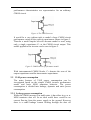
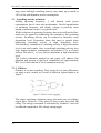
composed of a complimentary p- and n-nets as in figure 1.
Figure 1. CMOS structure, p- and n-nets.
2.1.1 The MOS transistor
The p- and n-nets in the CMOS circuit is build out of p- and nMOS6 transistors respectively. The n-MOS have two n-doped
regions in a bulk of silicon. The two regions are the source and
drain. A piece of polysilicon is laid in-between the source and
drain to form the gate. The p-MOS transistor is the same except p4
CMOS - Complementary Metal Oxide Semiconductor.
Invented by Wanless and Sah.
6
MOS - Metal Oxide Semiconductor.
5
3
Mixed RTL- and Gate-level Power Estimation with Low Power Design Iteration
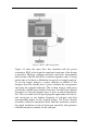
doped regions. A simple picture of the MOS transistor can be seen
in figure 2. When a positive voltage above the threshold voltage
Vt7 is applied to the n-MOS transistor gate, a conducting channel
is formed underneath the gate enabling a current to flow from
source to drain. The same applies for the p-MOS transistor except
a negative gate voltage is required.
Figure 2. Simplified picture the MOS transistor
Parasitic capacitance is formed between gate-source, gate-drain,
source-bulk, drain-bulk and gate-bulk. To understand the
performance of the transistor a model like the one in figure 3 is
used.
Figure 3. MOS parasitic model.
These capacitances have a large role in the performance of the
transistor, both in terms of speed and power consumption.
2.1.2 The CMOS inverter
The inverter is the simplest CMOS circuit. Here a single p- and nMOS transistor forms the p- and n-net. Figure 4 show the
schematic of the inverter. Even though simple, the inverter
7
Vt – The voltage for which the transistor changes state between conducting
and non-cunducting.
4
performance characteristics are representative for an arbitrary
CMOS circuit.
Figure 4. The CMOS inverter.
It would be a very tedious task to model a large CMOS circuit
performance using all the explicit capacitances shown in figure 3.
Therefor a much simpler but still accurate model is used, using
only a single capacitance CL at the CMOS circuit output. This
model applied to the inverter can be seen in figure 5.
Figure 5. CMOS inverter performance model.
With interconnected CMOS blocks, CL denotes the sum of the
output capacitance and the interconnect capacitance.
2.2 VLSI power consumption
The main features of VLSI power consumption can be
investigated based on the simple CMOS inverter performance
model and basic MOS transistor behavior. The power
consumption is divided into leakage, dynamic and static power
consumption.
2.2.1 Leakage power consumption
While the CMOS inverter is in stable state, it has either its p- or nMOS transistor shot off. In an ideal world there would be no
current flowing from the power supply to the ground. However
there is a small leakage current flowing through the shot off
5
Mixed RTL- and Gate-level Power Estimation with Low Power Design Iteration
transistor giving rise to leakage power consumption, specified by
formula 1.
P = I leak × Vdd
Formula 1.
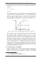
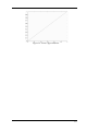
The dominating reason for the leakage current is the sub-threshold
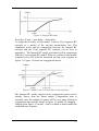
current. Below the threshold voltage Vt, at sub-threshold, the
transistor current approaches zero at zero gate-source voltage,
Vgs8. In figure 6 the transistor current Id is plotted at a
logarithmically scale against Vgs. As seen Id never becomes zero.
Figure 6. Transistor current I D plotted against Gate-Source voltage VGS.
The transistor current in the sub-threshold region is proportional to
gate voltage minus threshold voltage (Vg-Vt). A direct
consequence of this is an increase in leakage current with a
decrease of threshold voltage. It is an ongoing trend to decrease
the threshold voltage to increase speed and signal integrity. This
has lead to a constant increase of leakage current, which may
result in the leakage power consumption taking a dominating role
of the future VLSI power consumption. However, today the
leakage current is still small compared to other types of power
consumption. It is also due to MOS parameters and can not easily
be effected by the ASIC9 designer.
2.2.2 Dynamic power consumption
When the CMOS inverter switches from one state to another the
output capacitor CL have to be either charged or discharged.
Energy is consumed and transformed to heat in the MOS
8
9
6
Vgs – Voltage between gate and source.
ASIC - Application Specific Integrated Circuit.
transistors. The energy consumed is equal to the energy needed to
charge CL. The energy is specified according to formula 2.
E = Vdd × Q = Vdd × C L × Vswing
Formula 2.
Vdd is the power supply voltage and Vswing the voltage swing on
the output of the inverter. If the Vswing is the same as Vdd, which is
common, the energy becomes,
E = C L × Vdd
2
Formula 3.
The dynamic power consumption is the energy drawn from the
power supply during one second. The power consumed is
calculated as in formula 4, where f is the switching frequency.
1
2
P = × f × C L × Vdd
2
Formula 4.
CL is only charged at transition from low to high (zero to Vdd),
therefore the division by 2. In a general case, f symbolizes the
clock frequency. In this case the constant α is added to express the
switching activity as in formula 5.
P=
1
2
× α × f × C L × Vdd
2
Formula 5.
The constant α is between 0 and 1. With α equal to 1 there is
100% switching activity and formula 5 reduces to formula 4.
In the current CMOS technology the dynamic power consumption
constitutes up to 90% of the total power consumption. As seen
from the formula the dynamic power consumption depends on
parameters highly affected by the chosen design.
7
Mixed RTL- and Gate-level Power Estimation with Low Power Design Iteration
2.2.3 Short circuit power consumption
The inverter state transition is not instantaneous and at some point
both the p- and n-MOS transistors are conducting, creating a short
circuit current from power supply to ground. The current spike
produced has been showed to be of approximately rectangular
shape and the related power consumption can be approximated by
formula 6.
P=
1
× α × t × (Vdd + Vtp − Vtn )× I sc max
2
Formula 6.
Here t is the rise/fall time, Vtn and Vtp is the threshold voltage for
the n-MOS and p-MOS respectively and Iscmax is the maximum
short circuit current.
Iscmax is dependent on the load capacitance and the input versus
output rise/fall time. The best compromise has been shown to have
the input and output rise/fall time as equal as possible. The short
circuit power will then be reduced to approximately 10% of the
dynamic power consumption. The short circuit power
consumption is reduced even further with reduced supply voltage.
2.2.4 The effect of scaling
The main contributor to Moores law10 is the ongoing scaling of
transistor size. Scaling down the transistors has a large impact on
switching speed but also on power consumption. A smaller
transistor has less parasitic capacitance, which effectively increase
its speed. Smaller transistor on the other hand enables more
transistors, so there is no decrease in the total chip capacitance. At
the same time the supply voltage is scaled down to maintain an
acceptable electrical field over the gate dielectric. Formula 5 in
chapter 2.2.2 Dynamic power consumption shows that an increase
in f increases the power consumption while a decrease in supply
voltage decrease the power consumption. However, the decrease
in supply voltage has not been as big as the increase in clock
frequency. Also the chip die has constantly increased in size
leading to an increase in total chip capacitance. The higher
transistor count does also lead to an increasing need for
10
8
Doubling of computing power every 18:th month.
interconnect in more and more layers on the chip, increasing the
total chip capacitance even further.
The result is constantly higher power consumption. To cope with
this the switching activity, the total capacitance or the supply
voltage has to be reduced.
9
Mixed RTL- and Gate-level Power Estimation with Low Power Design Iteration
10
3
Power reduction techniques
As shown in the past chapter the dynamic power consumption is
the major contributor to VLSI power consumption. Formula 5
clearly shows which factors to scale to reduce power consumption.
The background information to this chapter is taken from [3] and
[4].
3.1 Voltage reduction
Scaling of supply voltage is of particular interest. Since P∝Vdd2 it
will have a significant effect on power consumption. However, at
the same time, the propagation delay td will increase as in formula
7, were β > 1.
td ∝
Vdd
(Vdd − Vt )β
Formula 7.
A reduction in supply voltage will therefore increase the delay. To
minimize delay loss Vt can be reduced somewhat. However, this
will have the effect of increased leakage power consumption as
was described in chapter 2.2.1 Leakage power consumption. Also,
as mentioned in chapter 2.2.4 The effect of scaling, scaling
transistor size implies scaling of supply voltage. The headroom to
further reduce supply voltage may therefore not be very large.
Even though supply voltage reduction has been the main action to
handle power consumption, it is today a balancing act between
power and speed. Even so, careful trade-off can achieve low
power consumption without loosing performance. The use of
lower supply voltage at less speed-sensitive parts is one such
example.
3.2 Capacitance reduction
Load capacitance is composed of the internal transistor
capacitance and wire capacitance. Better transistor technology and
careful layout of wires and gates can achieve capacitance
reduction. Special attention should be taken for on chip busses
with their long parallel wires with high wire-to-wire parasitic
capacitance and possibly high switching activity. Great effort
should be taken to reduce the capacitance in clock trees were their
11
Mixed RTL- and Gate-level Power Estimation with Low Power Design Iteration
long wires and high switching activity may make up as much as
50% of the total dynamic power consumption.
3.3 Switching activity reduction
Scaling operating frequency, f, will linearly scale power
consumption, but of cause also performance. Careful optimization
of operating frequency and supply voltage to precisely meet
timing constraints can give very good result.
While reduction of operating frequency has an overall good effect,
much can be gained by addressing the constant α, the switching
activity. Switching activity can be reduced in basically every
abstraction level. Experience show that most is gained when
addressing switching activity at high abstraction level.
Unfortunately, estimation of switching activity at high abstraction
level is not easily made. Also, even though switching activity have
large impact on power consumption, the product CL*α is of more
interest. But also CL is very hard to determine at high abstraction
level.
The power estimation method in this paper will address this
dilemma and present a high-level estimation tool (approximately
RTL-level) but with lower level estimation accuracy.
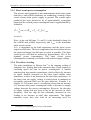
3.3.1 Glitches
Glitches is useless switching. They occur due to time differences
on input events, usually as a result of different logical depth as in
figure 7.
Figure 7. Glitch, useless toggling.
The output switching consumes energy the same way an ordinary
toggle does. However, if the glitch is short it may not reach full
swing. The energy consumed is calculated by formula 2, and will
be reduced compared to full voltage swing toggle.
12
4
Power estimation techniques
Power reduction has to be addressed at every design level, i.e.
system-, RTL-, gate- and transistor-level where most power can be
saved at the highest level. Good low power estimation is essential
for successful low power design. This chapter will give an
overview of the power estimation techniques used today on the
different levels. The background information to this chapter is
taken from [3] and [4].
4.1 System-level
At system-level, HW/SW co-simulators are often used to simulate
the performance of the entire system. The simulator co-simulates
predefined IP-blocks, such as µ-processors, memories, I/O’s etc,
together with HDL11 defined random logic. These simulators rely
on good, yet simple and fast performance models for the IPblocks. To my knowledge, most system level performance
simulator tools are more or less academic and have not, or just
very recently taken the step into the industry. At least if were
talking about performance in terms of power consumption.
4.2 RTL-level
While system-level power estimation is very new, power
estimation from RTL-level and down have had many years to
develop and mature. The traditional RTL-power estimation is
about ten years old, and can be divided into statistical- and
simulation-based estimation. The statistical-based estimation uses
component power statistics. It is very fast but not very accurate
and is of little interest. More interesting is the simulation-based
estimation since it provides much more accuracy.
Only architectural information of the hardware is known at RTLlevel. The first step in the power estimation is therefore
component power characterization and building of component
library. The components at issue are registers, adders, multipliers,
multiplexers etc. In many case component library may already be
at hand. Once power models for all components are available the
design is simulated together with the component power library
using suitable simulation vectors. The critical part in this flow is
of cause the component characterization.
11
HDL - Hardware Description Language
13
Mixed RTL- and Gate-level Power Estimation with Low Power Design Iteration
The components are characterized in terms of area, delay and
intrinsic switched capacitance (ISC). Area can be directly
measured from the layout and delay can be determined through
simulation or timing analysis programs. Determination of ISC,
which depends on input patterns, is more involving. The average
ISC of a module instance is the average capacitance that is
expected to switch when an input event toggles. ISC can be
determined by extracting a switch level model from a module
instance layout and simulating the switch level module using a
very long stream of randomly generated input patterns and
monitoring the capacitance switched per pattern.
The major drawback of this approach, except the tedious task of
component characterization, is that the power measure is an
average measure and only dependent on input switching activity,
not the actual input pattern. In reality the power consumption of
many components is very input pattern dependent. It is dependent
not only of the temporal input pattern, but also on the nature of an
input pattern sequence, i.e. spartial input pattern. For example the
power consumption of a ripple carry adder with a given input is
highly dependent of previous input.
This paper will present an alternative solution, integrated into the
original ASIC design flow, independent of predefined component
characterization and based on real signal annotation, not an
average measure.
4.3 Gate-level
Gate-level power estimation is in many ways a much easier task.
At gate level the design has been broken down to predefined gates
for which there exist accurate libraries. Either gate power models
are used in a similar way as for RTL-level simulation-based
estimation, or formula 5 in chapter 2.2.2 Dynamic power
consumption is used directly using the gate capacitance from the
gate library. The gate power models are basically a look up table
of the power consumed at a given input. The second model, using
formula 5, worked quite well in the past when the gate capacitance
was dominating. However, in recent days the wire capacitance is
dominating. Good wire capacitance estimation is therefore
essential for good accuracy in this type of power estimation. In
both cases simulation is performed using suitable simulation
vectors.
Gate-level is much closer to the final chip than RTL-level and the
power estimation is thereby more accurate. Also, at gate level the
14
power consumption is presented in more detail, per gate and not
per larger block as in RTL-level power estimation. The drawback
is higher computation complexity leading to longer estimation
time. It is also late in the design flow and the loop-back to higher
abstraction levels is often costly and painful.
The power estimation flow presented in this paper reach down to
gate-level taking advantage of good wire capacitance estimation of
modern design tools to perform accurate and detailed power
estimation.
4.4 Transistor-level
The most accurate power estimation is performed at transistorlevel. At this level the complete layout is known with complete
parasitic data. A comprehensive Spice like calculation can be done
to estimate the power consumption. However, if the design is large
the calculation may take very long time. A loop-back to perform a
major change could be very expensive.
Accurate transistor level performance in terms of power, speed
and area is essential for reusable blocks in order for higher level
tools to perform accurate performance estimation.
15
Mixed RTL- and Gate-level Power Estimation with Low Power Design Iteration
16
5
Our power estimation flow
Previous chapters have briefly described the advantages and
disadvantages with current power estimation methods at different
levels. The power estimation flow presented in this paper aim at
gate-level accuracy at RTL-level abstraction. It is not strictly
placed at a specific level, but instead integrated into the modern
ASIC design flow. The advantages of this are threefold. First, the
flow takes advantage of the information already gathered by other
design tools. It only requires a small third party tool to do the
actual power consumption calculation. Second, with an integrated
estimation flow, power estimation becomes a more natural part of
the ASIC design process. Fulfilling the power budget can be as
natural as fulfilling the time constants. The third advantage is
well-handled design iteration. This is of great importance since a
complete power estimation of a large design will be a heavy
computation task. The computation time may take days to perform
on a modern desktop. However, with good design iteration
complete power estimation is only needed once. The designer then
concentrates on the power hungry parts, which are dealt with
separately, each with considerable shorter estimation time.
5.1 Design tools
To understand the details of the power estimation flow, the design
tools need proper presentation. As will be described in chapter 6
Estimation tools, the power estimation flow is designed to work
with any design tool as long as necessary information is provided.
I have used Mentor graphics Modelsim as RTL-level simulator
and Cadence PKS (Physical Knowledge Synthesis) for gate-level
synthesis.
5.1.1 Mentor Graphics Modelsim
Modelsim is the discrete event simulator in Mentor Graphics HDL
design package. The simulator accepts hardware description
language VHDL or Verilog. A discrete event simulator works at
logical level were all transition is discrete values, logical 1, logical
0 and a number of other values such as X (undefined) and Z (high
impedance), etc. The simulator is build around a discrete event
table and a global clock. The discrete event table is like a time
calendar that is constantly updated during execution. At a given
time, the event listed in the table is executed and the table is
updated. The global clock advances to the next event in the table,
17
Mixed RTL- and Gate-level Power Estimation with Low Power Design Iteration
which is executed, and so the processes continue. By this
approach, only the time instance where an event occurs is
considered, with the advantage of simulation speedup.
The simulator is deterministic, which means that a given hardware
description and a given input sequence will always give in the
same result. This may not be the case if the events have zero
execution time. In that case there is no way to distinguish the
outcome of two order-dependent competition paths. The solution
to the problem is to introduce a minimum event execution delay,
the delta delay. The problem and its solution are shown
graphically in figure 8.
Figure 8. Maintaining determinism by using delta delay.
For the purpose of power estimation, Modelsim is used to analyze
gate-level node toggling. To accurately handle partial swing
toggling not only node toggling but also the time in-between
toggles is analyzed. For more information on Mentor graphics
Modelsim, see [5].
5.1.2 Cadence PKS
Cadence PKS (Physical Knowledge Synthesis) is the latest gatelevel synthesis from Cadence. The synthesizer reads HDL
18
description (VHDL or Verilog) together with a cell library and
generates a gate-level schematic. The cell library contain building
blocks for the gate-level schematic, such as AND-, OR -gates, flip
flops and buffers etc. The tool also needs timing and area
constraints in order to size gates and buffers and to optimize
placement.
Traditional gate level synthesis and place and route tools used
simple statistical wire load models to predict the wire delay. These
models were based on fan-outs12 and block size. This very simple
and crude model worked well in the past but increasingly bad in
modern technologies. The lack of physical wire delay knowledge
in the gate place and route made it very hard meet timing
constraints for the final design. Very many iteration steps between
gate and transistor level tool was required. PKS solve this problem
by introducing physical knowledge into the gate place and route.
PKS uses accurate timing analysis resulting in a close correlation
between timing at gate-level synthesis and timing after placement.
The result is much fast and very near optimal synthesis and gatelevel placement which is faster, smaller and less power consuming
than using traditional approach. PKS uses Seiner-tree or halfperimeter routines for estimation of wire length and Elmore delay
calculation to estimate the interconnect delay. The Seiner-tree
routine is more accurate than half-perimeter routine but slower,
the half-perimeter routine can be useful in a first quick synthesis.
For more information about Steiner-tree, half-perimeter, Elmore
calculation or more information about PKS in general, see [6] and
[8].
For the purpose of power estimation Cadence PKS is very useful.
It performs a quick and easy gate-level synthesis with accurate
estimation of wire capacitance and wire delay. A number of
standard formats exist to pass parasitic and delay information
between design tools. Cadence PKS support Standard Delay
Format (SDF) [7] and Reduced Standard Parasitic Format (RSPF)
[8]. SDF contain information on wire delay and gate delay for all
wires and gates. RSPF contain information on load parasitic for all
wires. Both SDF and RSPF are used in the power estimation flow.
PKS is also used to generate a Verilog netlist. It is a HDL
description of the design with the same behavior as the original
VHDL or Verilog description used as input to PKS, but with lower
level of abstraction. The Verilog netlist describes the gate-level
12
Fan-out - Number of block inputs connected to a block output.
19
Mixed RTL- and Gate-level Power Estimation with Low Power Design Iteration
schematic and contain all gate-level nodes. In the power
estimation flow this netlist is run in Modelsim to analyse gatelevel node toggling.
5.1.3 Other Design tools
The presented flow is targeted at Mentor Graphics Modelsim and
Cadence PKS. However, other similar design tools may be used as
long as they can supply enough design data, in this case wire-load,
wire-delay, gate-delay, RTL-level simulation result and process
data. The power estimation software (described in more detail in
chapter 6 Estimation tools) is designed for easy adaptation to
target other design tools.
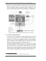
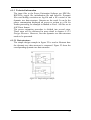
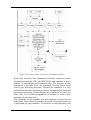
5.2 The flow
Figure 9 shows the part of a basic ASIC design flow covering
RTL-level and gate-level. After HDL is developed the complete
design is simulated and verified using Modelsim. Since the HDL
design often include a testbench and non-synthesizeable parts,
only a sub-part of the HDL description is passed to Cadence PKS
for gate-level synthesis and place and route. The gate-level netlist
together with placement information is then passed to transistorlevel place and route tools, possible Cadence Silicon Assembly.
20
Figure 9. Basic ASIC design flow.
Figure 10 show the same flow but extended with the power
estimation. HDL is developed as usual and a sub-part of the design
is passed to PKS for synthesis and place and route. Interconnect
data in form of RSPF and SDF is extracted together with a Verilog
netlist that is fed back to Modelsim for gate-level toggle analysis.
To do the toggle analysis a power stimulus is needed. If the
designer does not already have a power stimulus he can generate
one using the original testbench. This is done using a small piece
of software called Power Stimuli Generator. For the Power Stimuli
Generator to work the designer have to write a stimuli translationfile. This is a small text-file specifying the signal names for the inand in/out-puts to the highest hierarchy of sub-part and their
corresponding names in the original design. The Power Stimuli
Generator reads the simulation result from the testbench, extracts
the signal transitions on the in/inout-puts specified, and generates
a Modelsim macro stimulus for the sub-part.
21
Mixed RTL- and Gate-level Power Estimation with Low Power Design Iteration
When this is done the sub-part Verilog netlist can be simulated in
Modelsim using the power stimuli, generating a toggle list13. The
Power Estimation Software reads the toggle list together with
interconnect data and calculate the estimated power consumption.
Figure 10. Basic ASIC design flow extended with power estimation.
5.3 Low power design iteration
Since the power estimation of a large design may have long
execution time, it is essential with well-handled design iteration. It
would not be feasible to re-estimate the power for the complete
design every time a design modification has been made. Instead,
power estimation of the complete design is done only once, after
which the power hungry parts are handled separately.
The Power Stimuli Generator has a key role in this design
iteration. It generates a power stimulus for an arbitrary sub-part of
the design based on the original testbench stimuli. The input
stimulus for the isolated sub-part is identical with the input stimuli
for the sub-part in the complete design. This is absolutely essential
in order to get a comparable power estimation of the sub-part.
13
22
The toggle list is in reality the complete simulation result.
Typical power estimation iteration may look as follows (more
information about the individual steps can be found in chapter 6.
Estimation tools).
1. Perform power estimation on the complete design.
2. Re-design of the part of interest.
3. Write new stimuli translation-file and generate power stimuli
for the re-designed part.
4. Perform power estimation on the re-designed part.
5. Loop back to 2.
The low power design iteration achieves speedup in Cadence PKS
and in the Power Estimation Software. In PKS the speedup is
achieved due to smaller design to synthesize. In the Power
Estimation Software the speedup is achieved due to fewer nodes to
analyze.
I have not thoroughly investigated the magnitude of the speedup
but I estimate the estimation time to be at least linearly dependent
on the sub-part size. The speedup in each iteration can therefore be
expected to be of the same magnitude as the sub-part size
reduction.
A drawback is that no matter how small the sub-part is, the
complete design has to be simulated to generate the sub-part
power stimuli. However, this simulation time is small compared
with the PKS synthesis and Power Estimation Software execution
time.
5.4 The technique
The technique used to estimate the power consumption is fairly
straightforward. The idea is to gather information of toggling and
capacitance on every gate-level node and to calculate the dynamic
energy consumed on every node toggle based on formula 2 in
chapter 2.2.2 Dynamic power consumption. However, to assume
all node toggles to be full voltage swing would in most cases be a
too big overestimation. The main reason for this is glitches, which
often are to short in time to reach full swing. Other signals with
high toggle activity may also be of partial swing.
To calculate the voltage swing of a node, information of the time
between individual node toggle, gate-delay, wire-delay, node
capacitance and previous node voltage is needed. Full node
toggling information is acquired from Modelsim in form of the
toggle list. The toggle list contains all nodes that have toggled and
23
Mixed RTL- and Gate-level Power Estimation with Low Power Design Iteration
the time it occurred. The shortest toggle (glitch) is defined by the
delta-delay and is the shortest possible simulation step. In
Modelsim the delta delay is 1ns.
To estimate the behavior of the gate together with a wire, we need
to take a closer looks at the physical properties of the gate and the
wire. The on-chip wires act as a lossy transmission line that is
mainly capacitive. The analytical model of a RC transmission line
is a second order differential equation in two dimensions,
displacement x and time t.
∂ 2V
∂V
=
RC
∂t
∂x 2
Formula 8. Analytical model for the on-chip wire.
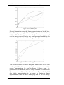
Simulation result of an on chip RC transmission line of different
length is presented in [9] and can be seen in figure 5.
Figure 11. Measured response of the on-chip wire.
The SDF-file supplied by Cadence PKS gate-level tool supplies
both gate-delay and wire-delay. The values are estimated by PKS
in order to perform a good gate-level layout. The gate-delay is the
delay from input to output measured at 50% of full swing voltage.
The measure is taken when the gate is driving an identical gate.
The wire-delay is the rise/fall time to 50% of full swing voltage.
The RSPF-file also supplied by PKS includes the wire load as a
lumped capacitor and the pin-to-pin delay modeled as a constant
voltage source driving a lumped RC network.
With the above information it is possible to make two models of
the gate transfer function.
24
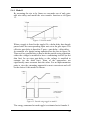
5.4.1 Model 1
By assuming the rise to be linear we can make use of only gateand wire-delay and model the wire transfer function as in figure
13.
Figure 12. Linear model.
When a toggle is listed in the toggle file, a delta delay has already
passed since the corresponding input was set to the gate input. The
effective gate delay is therefore T-gate = gate-delay - delta-delay.
An example of a partial swing transition can be seen in figure 14.
There are two possibilities to deal with the partial swing transition,
either the voltage is modeled to have a continuing rise/fall (as the
thin line) for an extra gate-delay or the voltage is modeled to
saturate (as the thick line). None of the approaches are
significantly more accurate then the other. For an implementation
point a view the saturating approach is most convenient and will
be the choice if this model is chosen.
Figure 13. Partial wing toggle in model 1.
The energy consumed at each toggle is estimated as in formula 8.
25
Mixed RTL- and Gate-level Power Estimation with Low Power Design Iteration
E=
1
× C × Vswing × Vdd
2
Formula 9.
The division by 2 is due to the fact that energy is only drawn from
the supply on transition from low to high. The formula for Vswing is
derived by a simple straight-line formula and gives formula 10.
Vswing
Vswing
Vdd
2 × T × (t + t d − Tgate ) − V p , transition ↑, t ≥ Tgate
wire
=
V − Vdd × (t − t + T ), transition ↓, t ≥ T
d
gate
gate
p 2 × Twire
≥ Vdd ⇒ Vswing = Vdd
Vswing ≤ 0 ⇒ Vswing = 0
Vswing = 0, t ≤ Tgate
Formula 10.
Here td is the delta delay, Vp is the previous voltage and Twire is the
wire-delay.
5.4.2 Model 2
In the RSPF-file a model of the pin-to-pin delay is modeled as the
delay of a lumped RC network. Judging from figure 12 and the
knowledge that the on chip wires are mainly capacitive, the gate
transfer function could be modeled as a RC network transfer
function, like the function in figure 14.
26
Figure 14. Lumped RC model.
Even here T-gate = gate-delay – delta delay.
To judge the accuracy of this model, I used a 10-pi segment RC
network as a model of the on-chip transmission line. The
simulation result and the comparison between the lumped RC
network and the 10-pi segment RC network can be seen in
appendix 1. The lumped RC model performed well in comparison
with the 10-pi segment RC model. However, neither of the models
compared very well with the measured on-chip wire response in
figure 11. Figure 15 shows an exaggerated sketch.
Figure 15. Model 1 and 2 vs. the actual on chip transition.
The lumped RC model requires more computation power and is
thereby slower than the linear model. Computation time is
essential since the number of nodes will be very many. Based on
computation time and the sketch in figure 15, model 2 is dropped.
Judging from figure 15, model 1 can be refined to better match the
measured wire response.
27
Mixed RTL- and Gate-level Power Estimation with Low Power Design Iteration
5.4.3 Refining model 1
Figure 16 shows a refinement of model 1 by introducing extra
wire-delay.
Figure 16. Better linear approximation.
In [9] a rule of thumb regarding lossy on-chip RC lines is
presented as,
T − wire = 0.4 × d 2 × R × C
Tr = d 2 × R × C
Formula 11. Rule of thumb.
Here T-wire is the wire-delay, R and C are resistance and
capacitance per unit length, d is the wire length and Tr is the risetime of the wire (from 10-90%). Since T-wire is already known
from the SDF-file, Tr can be rewritten as,
Tr =
T − wire
= 2.5 × T − wire
0 .4
Formula 12.
With this estimation of the rise-time and knowledge of the on-chip
wire behavior from figure 11, a two section linear approximation
is made. Using the estimation of Tr as 2.5×T-wire, T1 and T2 is
calculated. A linear approximation with a line trough origo and
with minimum distance to T-wire and T2 is used to calculate a
modified wire-delay, T-wire’. The approximation can be seen in
figure 14, the gate-delay have been excluded from this figure.
28
Figure 17. Calculation of modified wire-delay.
The modified wire-delay, T-wire’ becomes,
T − wire' = 1.63× T − wire
Formula 13.
For the full derivation of T-wire’, see appendix 2. Replacing Twire with T-wire’ in the equation for the estimated voltage swing
in formula 10 gives formula 14.
Vswing
Vswing
Vdd
3.26 × T × (t + t d − Tgate ) − V p , transition ↑, t ≥ Tgate
wire
=
Vdd
V −
× (t − t d + Tgate ), transition ↓, t ≥ Tgate
p 3.26 × Twire
≥ Vdd ⇒ Vswing = Vdd
Vswing ≤ 0 ⇒ Vswing = 0
Vswing = 0, t ≤ Tgate
Formula 14.
Here td is the delta delay, Vb is the previous voltage and Twire is the
wire-delay. This is the most appealing model and is the model
used in this power estimation method. Voltage saturation as
described in chapter 5.3.1 Model 1 will also be used.
29
Mixed RTL- and Gate-level Power Estimation with Low Power Design Iteration
5.4.4 Multiple fan-outs
The power consumption is estimated for each node. The wiredelay in the SDF-file is specified for every individual wire.
Naturally several wires may be connected one node. The question
is how to combine these several fan-out wire-delays to one totalwire delay to get representative power estimation. The situation is
described graphically in figure 18.
Figure 18. Multiple fan-outs
A transaction may be of full swing for one wire but partial for
another. There are two ways to address this problem. One way is
to look at each wire independently. The other way is to derive a, in
a power consumption view, representative wire-delay for the node.
Both solutions need knowledge about the individual wire
capacitance, which is unknown, only the Ctot is present in the
RSPF file. To find the individual capacitance an approximation
has to be made. The wire-delay of the wire is proportional to the
R×C. An increase of C is most likely due to an increase of the
wire length which in turn will give an equal increase in R.
Simultaneous increase in both C and R will give a relation
between C and wire delay as in formula 15, were α is a constant.
T − wire = α × C 2
Formula 15.
Some calculation gives formula 16 for the capacitance of an
arbitrary wire.
30
Cn =
C tot × t n
M
∑
m =1
tm
Formula 16.
Here Cn and tn is the capacitance and delay for wire n, and M is the
fan-out. Full derivation of the above formula can be found in
appendix 3. With this estimation of the individual wire
capacitance it is possible to do individual partial-swing voltage
calculations and sum up the power consumption for each node.
The problem with this method is the excessive amount of partial
swing calculations needed for a large design. A model using a
representative wire-delay for the node is more appealing since this
wire-delay only have to be derived once for each node. The main
problem with deriving this wire-delay is that the energy-time
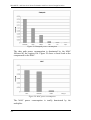
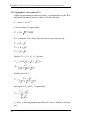
function is not a linear function. Figure 19 shows a Matlab
simulation if three different three-fan-out nodes. The final node
energy is normalized to 1 and the value on the x-axis is time units.
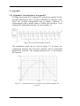
I tried to fit several differing polynomial functions, as can be seen
in figure 20, all without any satisfactory result.
Figure 19. Three different three-fan-out nodes.
31
Mixed RTL- and Gate-level Power Estimation with Low Power Design Iteration
Figure 20. Polynomial fits.
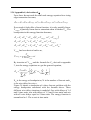
Several simulations show the linear approximation to be the best,
but still not good enough. A better linear approximation is shown
in figure 21. In this approximation the line starts from zero and
cuts the energy curve in such a way that I get equal probability for
over and under estimation of the energy consumption.
Figure 21. Better linear approximation.
The area in-between the linear and partly linear curve can be seen
as the probability for over- respectively under estimation of the
energy consumption. As seen in figure 21 those areas, i.e.
probabilities are identical, and for a large numbers of transactions
the energy error will be reduced to minimum. The method to find
this linear approximation is the same as finding a linear
approximation with the same underlying area as for the energy
32
function. The formula for the wire-delay for this representative
node wire-delay is expressed in formula 17.
N
T ' = 2 × max (Tn ) − ∑ (Tn − Tn −1 )(E n + E n −1 )
n =1
Tn = 3.26 × t n
N
V dd×Ctot m
1
× ∑ tk + tm ∑
Em = N
k =1
k = m +1 t k
t
∑ n
n =1
η=
T'
max(Tn )
t mod = max(tn ) ×η
Formula 17.
Here T’ is the time when the linear function reaches the
normalized energy, i.e. maximum energy for the node. tn is the
wire-delay and N is the fan-out. η is a positive value less or equal
to 1, specifying the wire-delay correction. tmod is the modified
wire-delay used to get a representative energy consumption for the
node. The full derivation of formula 17 and some Matlab
simulations verifying the result can be found in appendix 4.
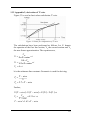
5.5 Future development of the several fan-out problem
If the calculation of a representative wire-delay turn out to be to
time consuming a possible solution would be to search for a
correlation between η for actual designs, and the fan-out number.
If a strong enough correlation exists, a simplified formula for the
wire-delay could be derived, speeding up the calculations.
33
Mixed RTL- and Gate-level Power Estimation with Low Power Design Iteration
34
6
Estimation tools
I have developed two tools with the purpose of the power
estimation. The main program, the Power Estimation Software is
designed to execute the power estimation technique described in
chapter 5.4 The technique, using the refined model 1 with
multiple-fan out wire-delay modification. The second program, the
Power Stimuli Generator is used to generate a stimulus for the
back-annotated Verilog netlist and to enable low power design
iteration.
6.1 Power Estimation Software
The first version of Power Estimation Software was developed and
executed in Matlab. This version did not take into account partial
swing and was thereby very much less complex then the final
version. Even so, it was terrible slow, and only small designs were
feasible for power estimation. The final version is designed in
C++ and uses a dynamic tree data structure which takes advantage
of the hierarchy of the design, giving a considerable execution
speedup compared to simple lookup tables. The program builds a
complete database, which can be quickly accessed to extract the
power consumption at any node or part, at any hierarchy of the
design.
6.1.1 Requirements
The current version of the Power Estimation Software is written
and compiled to work on Unix. In order to speed up the excessive
computation task the fastest possible computer should be used.
The power estimation requires large data storage capabilities,
preferable several tens of Gb. The data access time will influence
the execution time to a large extent and it is therefore preferred to
have local data storage.
The program requires an initialization-file that specifies search
paths and auto-save interval, etc. If the program is started without
such a file, the program can create an initialization-file template.
The initialization-file has to be located in the same directory as the
Power Estimation Software.
6.1.2 User guidance
Apart from filling out the initialization file template, the use of the
Power Estimation Software is straightforward. There is a couple of
commands available which all can be easily viewed by the help
command, “help”. The commands are:
35
Mixed RTL- and Gate-level Power Estimation with Low Power Design Iteration
all
This command performs complete power estimation. It performs
intermediate file translation, build data structure and calculate
power consumption. All these steps will be described in more
detail in the coming chapters.
hier
This command displays the loaded design hierarchy on screen.
Power
This command presents the power consumption. The command
can be executed alone or with a number of sub commands. The
possible combinations are:
power - the top level power consumption will be presented on
screen.
power all - all internal nodes and their power consumption will be
listed on screen.
power <node ore subunit> - the power consumption of the node
ore subunit will be presented on screen. Example, power n_101,
will present the power consumption on node n_101 on screen.
power <sub command> <filename> - adding a filename to the
above series of command will direct the output to a file by the
name specified by <filename>. <filename> have to be a complete
search
path.
Example,
power
all
~/final_project/power_example.txt
exit
This command will end the program.
The program performs several checks during execution. It does
not perform intermediate translation (described in chapter 6.1.3.2
Design structure) if it has already been done and no new in-data
exist. It also automatically reloads the data structure from file if it
exists. If the computer has crashed during power estimation, the
program starts by reloading the data structure from file before
continuing the power estimation procedure.
The log-file, help-file and all intermediate translator files are
saved in the same library as the Power Estimation program is
located.
All
files
will
be
automatically
named
<file_name>_<design_name>. For example, logfile_chip or
parasitics_chip.
36
6.1.3 Technical information
The input files to the Power Estimation Software are SDF-file,
RSPF-file, toggle file, initialization file and help-file. Dynamic
files used during execution are log-file and a file version of the
dynamic tree data structure. Outputs are the result. It can be the
power consumption displayed on screen or written to a file for
further processing for example in Matlab or Excel. All files are in
ASCII text format.
The power estimation procedure is divided into several steps.
These steps will be discussed in more detail in chapter 6.1.3.3
Design Structure. However, first the dynamic tree data structure
needs to be presented.
6.1.3.1 Data structure
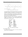
The simple design example in figure 22 is used to illustrate how
the dynamic tree data structure is composed. Figure 23 show the
corresponding dynamic tree data structure.
Figure 22. Simple design example.
37
Mixed RTL- and Gate-level Power Estimation with Low Power Design Iteration
Figure 23. Example dynamic tree data structure.
As seen the design is divided into three hierarchy levels. Note that
the inputs and outputs are represented at the second level, even
though they reach down to the third level. In the toggle file the
same in- or output signal may be represented at several levels. In
order not to count the same node several times the node is
represented only at the highest possible hierarchy. This is in my
point of view the most logical representation.
Each bubble, which I call a “knot”, has a number of variables and
dynamic lists associated to it. A list of these variables and the
variable type are presented in table 1. The dynamic lists add a
third dimension to the data structure.
node_name
instance
load
wire_delay
gate_delay
tot_power
time
logical_value
voltage
energy
String
String
Double
Double
Double
Double
Double list
Integer list
Double list
Double list
Table 1. List of variables and variable type.
6.1.3.2 Design structure
An overview of the design structure of the Power Estimation
Software can be seen in figure 24.
38
Figure 24. Design structure of the Power Estimation Software.
In the first step the Power Estimation Software extract all useful
information from the SDF- and RSPF-files and translate it into a
number of intermediate and formatted files. The purpose of this
translation is twofold. First, the translated files are much easier
read by the following processes. Second, the translator is a very
well defined interface between the Power Estimation Software and
the design tools used. If other design tool is going to be used, it is
fairly easy for a skilled programmer to modify or write a new
translator for this new tool.
The backbone of the dynamic tree data structure is based on the
node name. Wire-delay is presented per node. Gate-delay however
is presented per gate instance. To associate a both gate-delay and
39
Mixed RTL- and Gate-level Power Estimation with Low Power Design Iteration
wire-delay to a node an association between node name and
instance name is needed. This association is found in the RSPFfile and is presented in the parasitic file after translation.
To understand the steps in the power estimation a brief description
of the content in the translated files is useful.
Parasitic file
This file contains a table of node name, instance name and total
capacitance. The total capacitance is the sum of the gate output
capacitance and the wire capacitance.
Wire-delay file
This file contains a table of node name and wire-delay. Since a
node can have several wires (several fan-outs), several wire-delays
can be associated to one node name. In the SDF-file the wiredelay is presented both at transition from low to high and from
high to low. The wire-delay in the wire-delay file is the mean
value of these two.
Gate-delay file
This file contains a table of instance name and gate-delay. Even
here the gate-delay is the mean value of the gate-delay of
transition from low to high and from high to low.
Process file
This file contains information on parameters such as design
voltage and time scale.
Toggle file
This file contains full simulation information from Modelsim. It
contains a list of all transaction and at what time they happened.
The toggle file is actually a dump of the result in the list window
after running the power stimuli macro on the Verilog netlist from
Cadence PKS. More information about the generation of the
toggle file can be found in chapter 7 Power estimation step-bystep. The toggle file is left untouched by the translator. If another
design tool should be used instead of Modelsim the translator have
to be modified to generate a toggle file identical to this one.
Apart from the translator and the design structure the design is
composed of several operations, the major operations which will
be briefly described below.
40
Build data structure
This operation builds the dynamic three data structure backbone as
described in the previous chapter.
Add parasitic data
This operation adds data to the load, node name and instance
variable. Since the “Build data structure” operation is based on the
parasitic data file, the “Add parasitic data” operation is actually
performed simultaneously with “Build data structure”. Adding
variable data while each knot is created.
Add process data
This operation reads the process file and setting process variables.
Add wire-delay data
This operation first performs recalculation of the wire-delay
according to the multiple fan-out method described in chapter
5.3.4 Multiple fan-outs. After recalculation the new wire-delay
data is added to the wire-delay variable.
Add gate-delay data
This operation adds gate-delay data to the gate-delay variable.
Add toggle data
This operation adds the toggle information and performs voltage
swing, node energy and node power consumption calculation. The
heavy computing burden on this operation makes it the most time
consuming operation. The operation first adds a value to the
logical_value- and time-list for each knot. In the next step the
operation calculates the voltage swing and adds a value to the
voltage-list for each toggle based on the voltage swing formula 14
in chapter 5.3.3 Refining model 1. Next the energy consumed at
each toggle is calculated based on formula 9 in chapter 5.3.1
Model 1, and a value added to the energy-list. When the complete
toggle list has been processed the node total power consumption is
calculated by adding up the consumed energy of the node and
divide with the total execution time. The tot_power variable is set.
Finally the operation calculates the total power consumption on
higher hierarchy levels by adding up the power consumption on
lower levels. All knot variables and list are potentially set only for
the lowest level in the dynamic three data structure. At higher
41
Mixed RTL- and Gate-level Power Estimation with Low Power Design Iteration
level only the node_name, here representing subunit name, and
tot_power variables is set.
Read/write to log
These operation handles read and write to the log file. With large
designs the intermediate file translation may have significant
execution time. The Power Estimation Software uses the log-file
in order to keep track on what operation that has been performed.
It performs cross checks between log-file and file modification
dates in order not to retranslate already translated files.
Auto-save and auto-read back
Auto-save is essential since the power estimation of a large design
can take long time. Without this function a computer crash would
disastrous. The auto-save itself takes some time so the auto-save
interval should not be set to short, not less than a couple of hours
or so. The program uses the log-file to manage auto-save of the
data structure in ASCII format and to recreate the dynamic three
data structure from the auto-saved ASCII format data structure.
The auto-save interval is set in the initialization-file.
In case of a computer crash during power estimation, the Power
Estimation Software can easily be restarted. The program will then
read back the generated dynamic tree data structure from the
ASCII format data structure and automatically continue with the
power estimation procedure.
I/O operations
These operations handle the user interface and write the power
estimation result to screen or file.
6.2 Power Stimuli Generator
The Power Stimuli Generator is used to generate a stimulus for the
back-annotated Verilog netlist.
6.2.1 Description
In most cases only a part of the whole design can be synthesized at
gate-level. One example is memory, which usually is modeled in
HDL using a file. Also, for the purpose of power estimation
iteration, a power stimulus for a sub-part of the design is needed.
Most HDL designs are also tested using a testbench, which of
cause also is excluded at the gate-level synthesis. It would be very
impractical if the designer had to write separate power stimuli for
42
the sub-part. The purpose of the Power Stimuli Generator is to
enable the use of the complete HDL design with testbench as
power stimuli generator. Compared to the Power Estimation
Software this is a very simple program. It does two things. First it
generates a Modelsim macro file that adds the signals of interest.
Second it monitors the simulated signal activity of the original
HDL design and creates macro-based stimuli. The user specifies
the signals of interest by the stimuli translation-file.
6.2.2 Requirements
The program programmed and compiled for Unix. It requires an
initialization-file that specifies search paths. If the program is
started without such a file, the program can create an initializationfile template. The program also requires a stimuli translation-file.
The initialization-file has to be located in the same directory as the
Power Stimuli Generator.
6.2.3 User guidance
Before using the Power Stimuli Generator the initialization-file
template has to be filled out and a stimuli translator-file has to be
written. When this is done, the stimuli generator steps are as
follows.
1. Run the Power Stimuli Generator and generate the add-signal
macro.
2. Load the testbench of the original design into Modelsim and
make sure the list window is empty.
3. Run the add-signal macro.
4. Run the testbench and save the result in the list window with
the name and location you have specified in the Power Stimuli
Generation initialization-file.
5. Run the Power Stimuli Generator and generate a stimuli macro.
All output files are saved in the same library as the Power stimuli
Generator is located.
6.2.4 Technical information
An overview of the design structure of the Power Stimuli
Generator can be seen in figure 25. The inputs are Modelsim
simulation-file, stimuli translation-file and initialization-file.
Outputs are Modelsim macros for adding the signals of interest
and Modelsim stimuli macro. This program is designed for
43
Mixed RTL- and Gate-level Power Estimation with Low Power Design Iteration
Modelsim only. If other design tool is used this program has to be
modified or rewritten.
Figure 25. Design structure of the Power Stimuli Generator.
The program performs two functions, generate add-signal macro
and generate stimuli macro. For both operations the program
makes use of the stimuli translation-file. Figure 2 illustrates the
sub part in Modelsim, simulated using a testbench.
Figure 26. Subpart in testbench.
The subpart is the part that will be gate-level synthesized and the
part that need power stimuli. The stimuli translator-file specifies
the relation between the signal name in the testbench and the
corresponding signal name in the subpart. Two lines in the stimuli
translation-file may look as follows.
/testbench/io/clk /chip/clk
/testbench/io/freeze chip/freeze
44
All in- and in/out-signals has to be covered, but they are usually
not so many.
Generate add macro
This operation uses the stimuli translator-file to generate a
Modelsim macro file, which adds the signals of interest to the list
window in Modelsim. Two lines in the macro file may look as
follows.
add list /testbench/io/clk
add list /testbench/io/freeze
Generate stimuli macro
To generate the stimuli macro the program uses both the stimuli
translator-file and the Modelsim simulation-file. This file is a
direct dump of the simulation result when running the testbench
with the signals added by the add-signal macro. A couple of lines
in the generated stimuli macro file may look as follows.
force -freeze /chip/reset_n 1 @20
force -freeze /chip/clk 1 @21
force -freeze /chip/instr_bus 11000111111111100101100000 @21
force -freeze /chip/clk 0 @26
force -freeze /chip/clk 1 @30
45
Mixed RTL- and Gate-level Power Estimation with Low Power Design Iteration
46
7
Power estimation step-by-step
This chapter gives step-by-step guidance of how to perform the
power estimation based on design tools Cadence PKS and Mentor
Graphics Modelsim.
7.1 Generating power stimuli
The first step is the power estimation flow is to generate power
stimuli for the subpart of the design that will be synthesized by
Cadence PKS. The generation of the power stimuli should be
performed according to chapter 6.2 Power Stimuli Generator.
7.2 Performing a quick gate-level synthesis
The second step is to perform a gate-level synthesis of the subpart.
For this purpose of cause Cadence PKS have to be installed and
properly setup. For more information on installation and setup
please read to Cadence PKS user manual. The easiest way to
perform a quick gate-level synthesis is to fill out and run the
Cadence PKS script-file that are supplied with the estimation
tools. The script-file includes the following, in the order they
appear.
read_lef <library filename>
This command loads gate-level cell library. Several libraries may
be loaded.
Read_vhdl <VHDL filename>
or
Read_verilog <verilog finename>
These commands load the HDL description files. All files
included in the HDL design must be added.
do_build_generic -module <design name>
This command performs gate-level synthesis.
set_clock CLOCK -waveform {0 9} -period 18
set_clock_root -clock CLOCK clk
These commands add clock constraints. The waveform and period
have to be set according to the timing situation at hand. More
timing constants can obviously be set, but for the quick and easy
synthesis needed for power estimation clock constraints is
probable enough.
47
Mixed RTL- and Gate-level Power Estimation with Low Power Design Iteration
do_opimize –pks –effort [low medium high]
This command starts complete place and route optimization. The
effort can be set to low, medium and high. For a quick synthesis
the effort could be set to low.
do_extract_route_parasitcs <design name>.wdb
This command extracts the wire parasitic capacitance from the
design database.
write_sdf <spf filename>
write_spf –add_pks_rspf <rspf filename>
write_verilog –hierarchical –equation <netlist name>
These commands write the files needed for power estimation.
7.3 Performing toggle analysis
Next step is to analyze the node toggling of the Verilog netlist
created by Cadence PKS. This is done in Mentor Graphics
Modelsim. The procedure is as follows.
1. Compile the netlist, for example by using Compile menu ->
Compile, choose netlist and press open.
2. If the design is already compiled. Load the netlist, for example
by using the Simulate menu -> Simulate, choose design and
press load.
3. Add all signals in the design to the list window, for example
with the command add list -r/*.
1. Execute the power stimuli macro, for example using the Tool
menu -> Execute macro, choose macro and press open.
2. Save the result in the list window, for example by the
command write list -window .list -events <filename>. This file
is the toggle-file.
7.4 Performing power estimation
The last step in power estimation flow is to run the Power
Estimation Software. This should be done according to chapter 6.1
Power Estimation Software.
48
8
Power estimation verification and result
The verification of the result is limited due to lack of time. Power
Estimation Software verification was done by simulating a simple
design for a short period of time. The result was verified by hand
calculation. This verifies that the software, at least for that simple
design, calculated according to the derived method. To verify the
method, the result has to be comparing with the result from lower
level estimation tools, in this case a transistor-level. I did not have
time to learn two new tools and to perform the transistor-level
synthesis and power estimation. Therefor the result presented here
has not been verified and I can not guarantee its validity. I can
only state that the result seems fair.
The result in is from a rather small DSP design, simulated for 1ms
performing a FIR filter operation. Figure 27 show the overall most
power consuming nodes or units.
Figure 27. Overall power consumption.
Chip is the top level and the total power consumption of the
design. The most power-consuming node is the clock node, which
is expected. Second most power consuming is the Datapath,
followed by the MAC and the Multiplier. Figure 28 show a closer
look at the components in the data path.
49
Mixed RTL- and Gate-level Power Estimation with Low Power Design Iteration
Figure 28. Datapath power consumption.
The data path power consumption is dominated by the MAC
followed by the register file. Figure 29 show a closer look at the
components in the MAC.
Figure 29. MAC power consumption.
The MAC power consumption is totally dominated by the
multiplier.
50
9
Further development
There are no projects that can not be developed further and this is
no exception. In fact the plan is to form another final year project
to continue where I leave. First of all a better verification of the
method has to be done.
9.1 The flow
The most critical part of the flow is the toggle list, which can be
very big. The file contains redundancies since the same node can
be represented at several hierarchical levels, as described in
chapter 6.1.3.1 Data structure. This is an artifact of the Modelsim
command add list -r/*, which adds all signals in the design,
including the doublets. A workaround for this problem need to be
investigated to reduce the toggle list size and speed up power
estimation.
9.2 The technique
The technique calculates the power consumption based on
switching of node capacitance only, assuming this to be the major
part of the gate-level power consumption. The accuracy of this
approach i.e. the amount of internal gate power consumption
should be investigated. Though old, some guidance could probable
be found in [10]. Also, Spice simulation of a number of typical
VLSI gates to evaluate the internal power consumption would give
useful information. Finally the proposed development of the
several fan-out problem should be investigated as described in
chapter 5.4 Future development of the several fan-out problem.
9.3 The power estimation software
First of all the user interface need further development. The
internal structure holds much more information than can be
accessed by the current commands. Information at issue is node
capacitance, node toggle activity (percentage of clock) and better
display the design hierarchy associated with power consumption.
Display of consumed node energy as a function of time is also
easily implemented.
The efficiency of the code itself should also be looked into. I have
spent much time to make the software fast enough. Even so, I am
convinced that a skilled programmer can achieve better efficiency.
51
Mixed RTL- and Gate-level Power Estimation with Low Power Design Iteration
52
10 Summary and discussion
The aim of the thesis was to set up a power estimation flow to
estimate the power consumption at early design stage. I have
developed such a flow incorporating Mentor Graphics HDL
simulator Modelsim, Cadence PKS gate-level synthesis and power
estimation tools. The flow spans over both RTL- and gate-level to
achieve good accuracy at high abstraction level. I have developed
a suitable wire model to estimate partial swing toggling and I have
developed a first version of the power estimation tools. I have also
included support for low power design iteration for efficient power
estimation speedup when concentrating on smaller sub-parts of the
design.
The work has been very interesting and has given me good insight
in both low power VLSI design theory and the basic ASIC design
flow. More time was spent implementing the Power Estimation
Software than I initially estimated, mostly to get it time-efficient.
Unfortunately this led to lack of time for verification and full
development of the user interface of the Power Estimation
Software.
Nevertheless, I am satisfied with the result and hope someone will
continue with the work developing it into a powerful low power
design tool.
53
Mixed RTL- and Gate-level Power Estimation with Low Power Design Iteration
54
11 Dictionary
ASIC
CMOS
HDL
HW/SW
ISC
MAC
MOS
Netlist
n-MOS
p-MOS
PKS
RSPF
RTL
SDF
Verilog
VHDL
VLSI
Application Specific Integrated Circuit
Complementary Metal Oxide Semiconductor
Hardware Description Language (general term)
Hardware/Software
Intrinsic Switched Capacitance
Multiply And Accumulate
Metal Oxide Semiconductor
A HDL description of the gate-level schematic
n-doped Metal Oxide Semiconductor
p-doped Metal Oxide Semiconductor
Physical Knowledge Synthesis
Reduced Standard Parasitic Format
Register Transfer Level
Standard Delay Format
A common Hardware Description Language
A common Hardware Description Language
Very Large Scale Integration
55
Mixed RTL- and Gate-level Power Estimation with Low Power Design Iteration
56
12 References
[1] SIA, EECA, KSIA, JEITA, and TSIA, The International
Technology Roadmap for Semiconductors, 2001 edition, 2001.
[2] Jan M. Rabaey, Digital Integrated Circuits, Prentice Hall Inc,
1996, chapters 2 and 3.
[3] Wolfgang Nebel and Jean Mermet, Low power Design in Deep
Submicron Electronics, Kluwer Academic Publishers, 1997,
chapters 3, 4 and 6.
[4] Daniel Eckerbert, Deep Submicron Issues in RTL Power
Estimation, Department of Computer Engineering, Chalmers
University of Technology, 2002, chapters 1, 2 and 3.
[5] Mentor Graphics Modelsim user manual, accessed from the
program
[6] Cadence PKS user manual accessed from Open Book, supplied
with the program.
[7] IEEE std-1497-2001, IEEE Standard for Standard Delay
Format (SDF) for Electronic Design Process, 14 December 2001.
[8] Michael John Sebastian Smith, Application-Specific Integrated
Circuits, Addisson Wesley Longman, Inc, 1997, chapter 16 and
17.
[9] William J. Dally and John W. Poulton, Digital Systems
Engineering, Cambridge University Press, 1998, chapter 3.
[10] Alessandro Bogliolo, Luca Benini, Giovanni De Micheli and
Bruno Riccò. Gate-level Power and Current Simulation of CMOS
Integrated Circuits, IEEE transactions on very large scale
integration (VLSI) systems, vol. 5, no. 4, December 1997. Also
found
at:
http://akebono.stanford.edu/users/nanni/publications/archive/1997/
VSLISvol5iss4Dec97pg473.pdf [February 2003]
57
Mixed RTL- and Gate-level Power Estimation with Low Power Design Iteration
58
13 Appendix
13.1 Appendix 1, investigation of wire model 2
To judge the accuracy of a lumped RC network as a model for the
on-chip transmission line I needed something to compare with.
Since the on-chip transmission line is mainly capacitive I
experimented with a model using a CMOS gate driving a 10-pi
segment RC distributed network, as seen in figure 30.
Figure 30. 10-pi distributed RC network.
The simulation result can be seen in figure 31. It shows the
comparison between the 10-pi RC network and an equivalent
lumped RC network. The triangle-marked curve is the lumped
RC-network.
Figure 31. Comparison between 10-pi RC-network and a lumped RCnetwork.
59
Mixed RTL- and Gate-level Power Estimation with Low Power Design Iteration
Figure 32. Partial swing transitions.
A simulation of partial swing toggle can be seen in figure 32. As
seen the lumped RC network compare nicely with the 10-pi
network. However, due to several reasons, this wire model is not
used.
60
13.2 Appendix 2, derivation of T'-wire
Figure 33 is used as basis when calculating T'-wire.
Figure 33. Basis for computation of T'-wire.
The calculations have been performed as follows. Let Y1 denote
the equation of the first line section, Y2 the second section and Y3
the new linear approximation. The equations are,
Vdd
×t
2 × T − wire
0.4 × Vdd
Y2 =
×t
1.7 × T − wire
Y3 = k × t
Y1 =
k is the unknown line constant. Geometric is used for deriving,
T − wire
5
T2 = 2.7 × T − wire
T1 =
Further,
Y1 (T − wire ) − Y3 (T − wire ) = Y3 (T2 ) − Y2 (T2 ) ⇒
Vdd
× 0.31× t ⇒
T − wire
T − wire ' = 1.63 × T − wire
Y3 =
61
Mixed RTL- and Gate-level Power Estimation with Low Power Design Iteration
13.3 Appendix 3, derivation of Cn
Under the assumptions that wire-delay is proportional to the R×C
and that R increases linearly when C increase linearly.
T − wire = α × C 2
α is a constant. Or equivalent,
C = β × T − wire
β is a constant. For a three fan-out node we get respectively,
C1 = β × t1
C2 = β × t 2
C3 = β × t 3
Further Ctot = C1 + C2 + C3 giving,
Ctot = β ×
β=
(
)
t1 + t 2 + t 3 ⇒
Ctot
t1 + t 2 + t 3
(
)
which gives for C1
C1 =
(
Ctot × t1
t1 + t 2 + t 3
)
and equal or C2 and C3. Or generally
Cn =
Ctot × t n
M
∑
m =1
tm
Cn and tn is the capacitance and delay for wire n, and M is the fanout.
62
13.4 Appendix 4, derivation of η
For a three fan-out node the total node energy equation for a rising
edge transaction becomes,
Etot = C1 × Vdd × Vswing 1 + C 2 × Vdd × Vswing 2 + C3 × Vdd × Vswing 3
Even tough it looks like a linear function, it is only partially linear.
Vswingx is partially linear due to saturation when it reaches Vdd. The
breakpoints in this energy function becomes,
E1 = C1 × Vdd + Vdd × (C 2 × Vswing 2 + C3 × Vswing 3 )
2
2
2
2
2
E 2 = C1 × Vdd + C 2 × Vdd + Vdd × C3 × Vswing 3
2
E3 = C1 × Vdd + C 2 × Vdd + C3 × Vdd = Ctot × Vdd
2
Vswing has been derived earlier as,
Vswing =
Vdd
×t
3.26 × Twire
By insertion of Vswing and the formula for Cn, derived in appendix
3, into the energy equations we get the general equation,
N
V dd×Ctot m
1
Em = N
× ∑ tk + tm ∑
k =1
k = m +1 t k
t
∑ n
n =1
Em is the energy at breakpoint m, N is the number of fan-out and tx
is the wire delay for wire x.
Figure 34 shows a simulation of a three fan-out problem with the
energy breakpoints calculated with the formula above. Three
different wire delay situations is modeled. One with delays of 1,4
and 9 time units, one with delays of 1,2 and 9 time units and one
with all wire delays equal to 9 time units. The energy function is
normalized to 1. The x-axis is time units.
63
Mixed RTL- and Gate-level Power Estimation with Low Power Design Iteration
Figure 34. Energy consumed at a three fan-out node as a function of time.
I tried different polynomial fits to find a simple energy function.
Unfortunately a polynomial fit is in most cases very bad. In figure
35 polynomial mean-square fits of degree one to three is applied.
Figure 35. Different polynomial fits.
Linear fit is best but not good enough. A better linear
approximation is shown in figure 36.
64
Figure 36. Better linear approximation.
The area in-between the linear and partly linear curve can be seen
as the probability for over- respectively under estimation of the
energy consumption. The method to find this linear approximation
is the same as finding a linear approximation with the same
underlying area as for the energy function.
The area under the energy function is found by simple triangle and
square area calculations and becomes in the general case, for the
energy consumption function normalized to 1,
1 N
area1 = ∑ (Tn − Tn−1 )(E n + E n −1 )
2 n=1
N is the number of fan-outs, En and En-1 is the energy level at
breakpoint n respectively n-1, Tn and Tn-1 is the time for which the
breakpoints occur. T0 and E0 is zero and the time where the
breakpoints occur is,
Tn = 3.26 × t n
tn is the delay for wire n. The area for the linear approximation is
easier calculated and becomes,
area 2 =
1
(2 × max (Tn ) − T ')
2
65
Mixed RTL- and Gate-level Power Estimation with Low Power Design Iteration
T’ is the time when the linear approximation reaches 1 and
saturates. Setting area1=area2 gives,
N
T ' = 2 × max(Tn ) − ∑ (Tn − Tn−1 )(En + En−1 )
n =1
here Em is calculated as before,
N
V dd ×Ctot m
1
Em = N
× ∑ tk + tm ∑
k =1
k = m +1 t k
∑ tn
n =1
Finally the constant η becomes,
η=
T'
max (Tn )
Figure 37 and 38 shows the result of the linear approximation on
the other two fan-out examples. The third example, which already
is linear function, gives η=1.
Figure 37. Linear approximation.
66
Figure 38. Linear approximation.
67
På svenska
Detta dokument hålls tillgängligt på Internet – eller dess framtida ersättare –
under en längre tid från publiceringsdatum under förutsättning att inga extraordinära omständigheter uppstår.
Tillgång till dokumentet innebär tillstånd för var och en att läsa, ladda ner,
skriva ut enstaka kopior för enskilt bruk och att använda det oförändrat för
ickekommersiell forskning och för undervisning. Överföring av upphovsrätten
vid en senare tidpunkt kan inte upphäva detta tillstånd. All annan användning av
dokumentet kräver upphovsmannens medgivande. För att garantera äktheten,
säkerheten och tillgängligheten finns det lösningar av teknisk och administrativ
art.
Upphovsmannens ideella rätt innefattar rätt att bli nämnd som upphovsman i
den omfattning som god sed kräver vid användning av dokumentet på ovan
beskrivna sätt samt skydd mot att dokumentet ändras eller presenteras i sådan
form eller i sådant sammanhang som är kränkande för upphovsmannens litterära
eller konstnärliga anseende eller egenart.
För ytterligare information om Linköping University Electronic Press se
förlagets hemsida http://www.ep.liu.se/
In English
The publishers will keep this document online on the Internet - or its possible
replacement - for a considerable time from the date of publication barring
exceptional circumstances.
The online availability of the document implies a permanent permission for
anyone to read, to download, to print out single copies for your own use and to
use it unchanged for any non-commercial research and educational purpose.
Subsequent transfers of copyright cannot revoke this permission. All other uses
of the document are conditional on the consent of the copyright owner. The
publisher has taken technical and administrative measures to assure authenticity,
security and accessibility.
According to intellectual property law the author has the right to be
mentioned when his/her work is accessed as described above and to be protected
against infringement.
For additional information about the Linköping University Electronic Press
and its procedures for publication and for assurance of document integrity,
please refer to its WWW home page: http://www.ep.liu.se/
© Jesper Nilsson