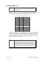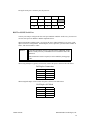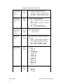
1
CMD17686GX
cpuModuleTM User’s Manual
RTD Enhanced Award BIOS Versions 4.51.xx
(Real Time Devices)
ISO9001 and AS9100 Certified
BDM-610000017
Rev. B
CMD17686GX
cpuModuleTM
User’s Manual
RTD Embedded Technologies, INC.
103 Innovation Blvd.
State College, PA 16803-0906
Phone: +1-814-234-8087
FAX: +1-814-234-5218
E-mail
[email protected]
[email protected]
web site
http://www.rtd.com
Revision History
Rev. A) New namual naming method
Rev. B) Added multiPort (aDIO)
Published by:
RTD Embedded Technologies, Inc.
103 Innovation Blvd.
State College, PA 16803-0906
Copyright 1999, 2002-2004 by RTD Embedded Technologies, Inc.
All rights reserved
Printed in U.S.A.
The RTD Logo is a registered trademark of RTD Embedded Technologies. cpuModule and utilityModule
are trademarks of RTD Embedded Technologies. PS/2, PC/XT, PC/AT and IBM are trademarks of International Business Machines Inc. MS-DOS, Windows, Windows 95, Windows 98 and Windows NT are trademarks of Microsoft Corp. PC/104 is a registered trademark of PC/104 Consortium. All other trademarks
appearing in this document are the property of their respective owners.
Chapter 1: Introduction . . . . . . . . . . . . . . . . . . . . . . . . . . . . . . . . . . 7
The CMD17686GX cpuModule .......................................................8
Specifications ....................................................................................10
Chapter 2: Getting Started . . . . . . . . . . . . . . . . . . . . . . . . . . . . . . . . 13
Basic Connector Locations ...............................................................14
Fail safe boot ROM ...........................................................................16
Cable Kits .........................................................................................17
Connecting Power .............................................................................18
Connecting the utility cable ..............................................................19
Connecting a Keyboard ....................................................................20
Connecting to the PC/104 Bus ..........................................................21
Connecting to the PC/104-Plus PCI Bus ..........................................22
Default Configuration .......................................................................24
Booting to Boot Block Flash with Fail Safe Boot ROM ..................26
If You Misconfigure the cpuModule ................................................27
For More Information .......................................................................28
Chapter 3: Connecting the cpuModule . . . . . . . . . . . . . . . . . . . . . . 31
I/O Connections ................................................................................32
Connector Locations .........................................................................33
Auxiliary Power, CN3 ......................................................................35
Advanced Digital I/O Ports (aDIO), multiPort CN6 ........................37
Serial Port 1, CN7 .............................................................................38
Serial Port 2, CN11 ...........................................................................41
multiPort Parallel Port, CN6 .............................................................44
Multifunction Connector, CN5 .........................................................46
Bus Mouse Connector, CN4 .............................................................48
USB Connector,CN17 ......................................................................49
PC/104 Bus, CN1 and CN2 ..............................................................50
Chapter 4: Configuring the cpuModule (BIOS Setup) . . . . . . . . . 55
Entering the BIOS Setup ...................................................................56
Default Configuration .......................................................................57
Disabling Fail Safe Boot ROM .........................................................59
Installing SSD Memory ....................................................................60
Quick Boot Description ....................................................................61
Configuring with the RTD Enhanced Award BIOS .........................62
Chapter 5: Using the cpuModule . . . . . . . . . . . . . . . . . . . . . . . . . . . 77
Memory Map ....................................................................................78
Input/Output Address Map ...............................................................79
Hardware Interrupts ..........................................................................81
The RTD Enhanced Award BIOS ....................................................82
Power On Self Tests (POSTs) ..........................................................83
RTD Enhanced Award BIOS POST Codes ......................................86
Default Configuration .......................................................................89
Direct Hardware Control ..................................................................91
Advanced Digital I/O Ports (aDIO) ..................................................92
Basic Interrupt Information for Programmers: .................................96
Watchdog Timer Control ..................................................................99
Real Time Clock Control ..................................................................100
Parallel Port Control .........................................................................101
Processor Clock Control ...................................................................102
Storing Applications On-board .........................................................103
Ways to Use the Solid State Disk Socket .........................................104
Using BIOS Extension Devices ........................................................105
Using Conventional Solid State Devices ..........................................106
Chapter 6: Hardware Reference . . . . . . . . . . . . . . . . . . . . . . . . . . . 109
Jumpers .............................................................................................110
Jumpers and Default Jumper Settings ...............................................112
Solder Jumpers ..................................................................................113
Mechanical Dimensions ....................................................................114
686GX Processor Thermal Management .........................................115
Chapter 7: Troubleshooting . . . . . . . . . . . . . . . . . . . . . . . . . . . . . . . 117
Common Problems and Solutions .....................................................118
Troubleshooting a PC/104 System ...................................................121
How to Obtain Technical Support ....................................................122
How to Return a Product ..................................................................123
Chapter 8: Limited Warranty . . . . . . . . . . . . . . . . . . . . . . . . . . . . . 125
CHAPTER 1: INTRODUCTION
This manual is meant for users developing with the CMD17686GX
cpuModule. It contains information on hardware and software of
the cpuModule.
READ THE SPECIFICATIONS FIRST.
The manual is organized as follows:
CMD17686GX
Chapter 1:
Introduction
Introduces main features and specifications.
Chapter 2:
Getting Started
Provides abbreviated instructions to get started.
Chapter 3:
Connecting the cpuModule
Provides information on connecting the cpuModule to peripherals.
Chapter 4:
Configuring the cpuModule
Provides information on configuring hardware and software.
Chapter 5:
Using the cpuModule
Provides information needed to develop applications for the cpuModule.
The chapter includes general information on the cpuModule, plus detailed information on storing applications and system functions, and using utility programs.
Chapter 6:
Hardware Reference
Lists jumpers and their locations and mechanical dimensions.
Chapter 7:
Troubleshooting
Offers advice on debugging problems with your system.
Chapter 8:
Warranty
RTD Embedded Technologies, Inc.
The CMD17686GX cpuModule
The PC/104 cpuModules described in this manual are designed for industrial applications which require:
•
•
•
•
•
•
software and hardware compatibility with the PC/AT world
high-speed "number-crunching" operation
low power consumption
small physical dimensions
high reliability
good noise immunity
This cpuModule is highly integrated, combining all major functions of a PC/AT computer on one
compact board. It integrates all primary I/O functions of a AT compatible computer:
•
•
•
•
•
•
•
a keyboard interface
a switchable (ECP/EPP parallel port) or (16 bits of digital I/O) multiPort
two versatile RS232/422/485 serial ports
a Real Time Clock
a speaker port
a PS/2 mouse port
two USB ports
It also enhances standard AT-compatible computer systems by adding:
•
•
•
•
•
one Solid State Disk socket
two Solid State Disk sockets
a non-volatile configuration without a battery
a Watchdog Timer
Fail Safe Boot ROM
The next figure shows a simplified block diagram of the cpuModule:
CMD17686GX
8
RTD Embedded Technologies, Inc.
32 or 128 MB
SDRAM
Two USB ports
MediaGX MMX
Enhanced
Processor
RTD Enhanced
BIOS
Cx5530 I/O
Companion
PC/104 ISA Bus
And
PC/104 Plus PCI Bus
IEEE 1284
Parallel Port
RS-232/422/485
Serial Port
RS-232/422/485
Serial Port
National
PC97317
Super I/O
RTC
Keyboard
Watchdog Timer
You can easily customize the cpuModule by stacking PC/104 modules such as video controllers,
modems, LAN controllers, or analog and digital data acquisition modules. Stacking PC/104 modules
on the cpuModule avoids expensive installations of backplanes and card cages and preserves the
module's compactness.
RTD Enhanced Award BIOS is also implemented in the cpuModule. This BIOS supports ROMDOS™, MS-DOS and Windows operating systems. Drivers in the BIOS allow booting from floppy
disk, hard disk, Solid State Disk, boot block flash, or DiskOnChip®, thus enabling the system to be
used with traditional disk drives or non-mechanical drives.
The cpuModule and BIOS are also compatible with most real-time operating systems for PC compatible computers, although these may require creation of custom drivers to use the SSD and watchdog timer.
CMD17686GX
RTD Embedded Technologies, Inc.
9
Specifications
CMD17686GX233
•
•
•
•
•
National Semiconductor Geode MMX enhanced microprocessor
233 MHz clock speed
2.0 V processor supply (provided on-board)
16 KB L1 cache
Math coprocessor
CMD17686GX300
•
•
•
•
•
National Semiconductor Geode GX1 MMX enhanced microprocessor
300 MHz clock speed
2.0 V processor supply (provided on-board)
16 KB L1 cache
Math coprocessor
CMD17686GX333
•
•
•
•
•
National Semiconductor Geode GX1 MMX enhanced microprocessor
333 MHz clock speed
2.2 V processor supply (provided on-board)
16 KB L1 cache
Math coprocessor
DMA, Interrupts, Timers
•
•
•
Six (6) DMA channels (8237 compatible)
Fifteen (15) interrupt channels (8259 compatible)
Three (3) counter/timers (8254 compatible)
•
2 USB 1.0 ports
USB ports
Advanced Digital I/O (aDIO)
•
•
•
•
•
•
Two 8 bit, TTL compatible, programmable Digital I/O Ports.
One port is bit direction programmable and the other is byte direction programable.
Advanced Interrupt modes
Interrupt on change
Interrupt on match
Interrupt on strobe
Memory Configurations
•
•
•
32MB
128MB
256MB
Fail-safe Boot ROM
•
•
CMD17686GX
10
Surface mount Flash chip that holds ROM-DOS™
Replaces the previous DiskOnChip®
RTD Embedded Technologies, Inc.
Solid State Disk Sockets
•
SSD sockets can hold one of the following Conventional SSD devices.
Device
Atmel 5V Flash
SRAM
NOVRAM
EPROM
AMD 5V Flash
Full Read/Write
Access
yes
yes
yes
Read Only
Read Only
Device
DiskOnChip®
2000
DiskOnChip®
1000
MCSI PromDisk
128Kbytes
256Kbytes
512Kbytes
1Mbyte
yes
yes
yes
yes
yes
yes
no
no
yes
no
yes
yes
yes
yes
yes
no
no
no
yes
no
Full Read/Write
Access
yes
Maximum Number per
Sizes
cpuModule
1
16MB - 1GB *
yes
1
1MB, 2MB
yes
1
4MB, 8MB *
(*) Larger devices may be available in the future.
Peripherals
•
•
•
•
•
•
•
•
Two serial ports software configurable for RS232/422/485; baud rates from 50 to 115200
baud in 16450 and 16550A compatible mode and 1.5 Mbaud in Extended UART mode
Parallel port with SPP, ECP, EPP capability and selectable interrupts and DMA channel
16 bits of digital I/O
PC/AT standard keyboard port
A PS/2 mouse port
PC speaker port
Real Time Clock (requires user-supplied external battery for date and time backup)
Watchdog Timer with time-out of 1.2 seconds
•
•
•
•
•
RTD Enhanced Award BIOS
Directly supports Solid State Disk (SSD) and M-Systems’ DiskOnChip®
User-configurable using built-in Setup program
Nonvolatile configuration without a battery
Can boot from floppy disk, hard disk, Solid State Disk, or fail-safe boot ROM
BIOS
CMD17686GX
RTD Embedded Technologies, Inc.
11
Connections
•
•
•
•
•
•
•
•
•
•
AT bus, per PC/104 specifications (64-pin CN1, 40-pin CN2)
Auxiliary Power Connector (12-pin CN3)
PS/2 Mouse Connector (4-pin CN4)
Multifunction connector (10-pin CN5)
multiPort (26-pin CN6)
Serial port 1 connector (10-pin CN7)
Serial port 2 connector (10-pin CN11)
PCI bus, per PC/104-Plus specifications ()
Dual USB port connector(10-pin CN17)
Two 8 bit Digital I/O Ports ( CN6)
Physical Characteristics
•
•
•
Dimensions: 3.55 x 3.775 x 0.6 inches (90 x 95.9 x 16mm)
Weight (mass): 4.16 ounces (118 grams)
PCB: 12-layer, mixed surface-mount and thru-hole
Operating environment
•
•
•
•
Power supply: 5V +/- 5%, 10 Watts
686 processor operating temperature: -40 to +85 degrees C case (with proper cooling) See
686GX Processor Thermal Management
Operating relative humidity: 0 to 95%, non-condensing
Storage temperature :-55 to +125 degrees C.
Power Consumption
Exact power consumption depends on the peripherals connected to the board, the selected SSD configuration and the memory configuration.
The table below lists power consumption for typical configurations and clock speeds:
Module
Consumption, typ.
RAM
SSD
Coprocessor
CMD17686GX233
233 MHz
5.0 W
32 or 128
or 256
MB
None
Internal
CMD17686GX300
300 MHz
6.1 W
32 or 128
or 256
MB
None
Internal
CMD17686GX333
333 MHz
6.3W
32 or 128
or 256
MB
None
Internal
CMD17686GX
12
RTD Embedded Technologies, Inc.
CHAPTER 2: GETTING STARTED
For many users, the factory configuration of the cpuModule can be used
to get a PC/104 system operational. If you are one of these users, you can
get your system up and running quickly by following a few simple steps
described in this chapter. Briefly, these steps are:
• Connect power.
• Connect the utility cable.
• Connect a keyboard.
• Default Bios Configuration
• Fail Safe Boot ROM
Refer to the remainder of this chapter for details on each of these steps.
CMD17686GX
RTD Embedded Technologies, Inc.
13
Basic Connector Locations
The following figure(s) and table show the connectors used in this chapter
CMD17686GX
14
RTD Embedded Technologies, Inc.
CMD17686GX Basic Connector Locations
Connector
Function
Size
CN1
PC/104 Bus (XT)
64 pin
CN2
PC/104 bus (AT)
40 pin
CN3
Auxiliary power
12 pin
CN4
PS/2 Mouse
4 pin
CN5
Multifunction
10 pin
CN6
multiPort
26 pin
CN7
Serial Port1
10 pin
CN11
Serial Port2
10 pin
CN17
USB Connector
10 pin
For a complete listing of connectors, please refer to I/O Connections.
NOTE!
CMD17686GX
Pin 1 of each connector is indicated by a square solder pad on the bottom of the PC board and a white square silkscreened on the top of the
board.
RTD Embedded Technologies, Inc.
15
Fail safe boot ROM
Fail Safe Boot ROM is supplied with the board. This feature is programmed into a surface mount flash chip. The programmed boot ROM is ROM-DOS™. Fail Safe Boot ROM allows
the system to boot without any attached storage devices. i.e. floppy, IDE, SSD. Installing jumper
JP5 will force the cpuModule to use fail safe boot ROM. This configuration allows you to boot to
non-volatile onboard ROM-DOS™.
CMD17686GX
16
RTD Embedded Technologies, Inc.
Cable Kits
For maximum flexibility, cables are not provided with the cpuModule. You may wish to purchase
our cable kit for the cpuModule.
The XK-CM33 cable kit contains the following:
•
•
•
•
•
•
CMD17686GX
Multifunction utility cable (keyboard socket, battery, reset, speaker)
Two serial port cables (DIL10 to DSUB9)
multiPort port cable (DIL26 to DSUB25)
Power cable (DIL12 to wire leads)
Dual USB cable (4 Pin SIL to USB)
PS/2 Mouse adapter (4 Pin DIL to PS/2 Female)
RTD Embedded Technologies, Inc.
17
Connecting Power
WARNING!
If you improperly connect power, the module will almost certainly be
damaged or destroyed. Such damage is not warranted! Please verify
connections to the module before applying power.
Power is normally supplied to the cpuModule through the PC/104 bus, connectors CN1 and CN2. If
you are placing the cpuModule onto a PC/104 stack that has a power supply, you do not need to make
additional connections to supply power.
If you are using the cpuModule without a PC/104 stack or with a stack that does not include a power
supply, refer to Auxiliary Power, CN3 for more details.
CMD17686GX
18
RTD Embedded Technologies, Inc.
Connecting the utility cable
The Multifunction connector CN5, implements the following interfaces:
•
•
•
•
AT keyboard
Speaker output
System reset input
Battery input
To use these interfaces, you must connect to the Multifunction connector, making sure the orientation of pin 1 is correct. If you are using the Multifunction cable from our cable kit, the cable provides
a small speaker, a 5-pin circular DIN connector for the keyboard, a push-button for resetting the PC/
104 system, and a lithium battery to provide backup power to the Real Time Clock.
To connect individual devices to the Multifunction connector, please see Multifunction Connector,
CN5
CMD17686GX
RTD Embedded Technologies, Inc.
19
Connecting a Keyboard
You may plug a PC/AT compatible keyboard directly into the circular DIN connector of the Multifunction cable in our cable kit.
NOTE!
Some newer keyboards may use a smaller "mini-DIN" connector; you
will need an adapter to plug these keyboards into the cpuModule.
These connectors are available for order instead of the default circular
DIN connector.
Many keyboards are switchable between PC/XT and AT operating
modes, with the mode usually selected by a switch on the back or bottom of the keyboard. For correct operation with this cpuModule, you
must select AT mode.
CMD17686GX
20
RTD Embedded Technologies, Inc.
Connecting to the PC/104 Bus
The PC/104 bus connectors of the cpuModule are simply plugged onto a PC/104 stack to connect to
other devices.
We recommend you follow the procedure below to ensure that stacking of the modules does not
damage connectors or electronics.
WARNING!
Do not force the module onto the stack! Wiggling the module or applying too much pressure may damage it. If the module does not readily
press into place, remove it, check for bent pins or out-of-place keying
pins, and try again.
• Turn off power to the PC/104 system or stack.
• Select and install standoffs to properly position the cpuModule on the PC/104 stack.
• Touch a grounded metal part of the rack to discharge any buildup of static electricity.
• Remove the cpuModule from its anti-static bag.
• Check that keying pins in the bus connector are properly positioned.
• Check the stacking order; make sure an XT bus card will not be placed between two
AT bus cards or it will interrupt the AT bus signals.
• Hold the cpuModule by its edges and orient it so the bus connector pins line up with
the matching connector on the stack.
• Gently and evenly press the cpuModule onto the PC/104 stack.
CMD17686GX
RTD Embedded Technologies, Inc.
21
Connecting to the PC/104-Plus PCI Bus
The cpuModule is simply plugged onto a PC/104 stack. Other PC/104-Plus boards may then connect to the cpuModule’s PC/104-Plus bus connector. Supplying power to the PCI bus is provided
by the cpuModule.
We recommend you follow the procedure described for the PC/104 bus.
There are three additional considerations when using the PCI bus, PCI Bus signaling level, the slot
selection switches on add in boards, and 3.3 volt power source for the expansion cards.
Slot Selection Switches
Unlike PC/104 cards, PC/104 Plus expansion cards have a "slot" selection switch or jumpers. In
total, there are 4 PCI cards that can be stacked onto the cpuModule with switch positions 0 through
3. The distance from the CPU determines these switch settings. The card closest to the CPU is said
to be in slot 0, the next closest slot 1 and so on to the final card as slot 3.
The "slot" setting method may vary from manufacturer to manufacturer, but the concept is the same.
The CPU is designed to provide the correct delay to the clock signals to compensate for the bus
length. The correct switch setting ensures the proper clock delay setting, interrupt assignment, and
bus grant/request channel assignment. Refer to the expansion board’s manual for the proper settings.
Each expansion card must be in a different slot.
PCI Bus Expansion Card Power
+5 Volt DC
The +5 volt power pins on the PC/104 Plus PCI bus are directly connected to the +5 volt pins on the
PC/104 connector and the power connector CN3 (pins 2 and 8). +5 volt expansion boards can be
powered directly from these pins.
+3.3 Volt DC
The default source for the +3.3 volt power pins on the PC/104 Plus PCI bus is an on board power
converter. The on-board +5 volt to +3.3 volt converter is capable of suppling a maximum of 2 amps
of 3.3 volts to the PCI bus. If 2 amps is not enough change solder blob BL1 from 1 and 2 to 2 and 3
. This change will connect the 3.3 volt power pins on the PCI bus to pins 10 and 12 on power connector CN3 .. This change will allow a new power source, connected to the power connector CN3,
to drive the 3.3 volt power pins on the PCI bus.
Booting the cpuModule for the First Time
You can now apply power to the cpuModule. You will see a greeting message from the VGA BIOS
and then:
CMD17686GX
22
RTD Embedded Technologies, Inc.
•
•
the cpuModule BIOS version information
a message requesting you press {Del} to enter the Setup program
If you don’t press {Del}, the cpuModule will try to boot from the current settings.
If you press {Del}, the cpuModule will enter Setup. Once you have configured the cpuModule using
Setup, save your changes and reboot.
NOTE!
By default, boards are shipped with fail safe boot ROM enable.
When Fail Safe Boot ROM is enabled the system will boot to it exclusively.
CMD17686GX
RTD Embedded Technologies, Inc.
23
Default Configuration
In addition to the Setup configuration stored on the board, the cpuModule has a permanent default
configuration. The system will resort to using this default if an error occurs when accessing the
EPROM which holds the Setup on the module.
The default configuration is listed below.
BIOS Default Configuration
Function
Default selection
IDE Interface 0 Master
IDE Interface 0 Slave
IDE Interface 1 Master
IDE Interface 1 Slave
Boot device
BIOS Extension
Floppy Drive 1
Floppy Drive 2
Serial port 1
Serial port 2
Keyboard
USB
Fail safe boot ROM
Select Active Video
Power Management
PNP OS Installed
Resources Controlled By
PCI IRQ Activated By
IDE HDD Block Mode
KBC Input Clock
SSD Window
Halt On
Virus Warning
CPU Internal Cache
Cyrix 6X86/MII CPUID
Swap Floppy Drive
Boot Up Numlock Status
Gate A20 Option
Security Option
Report No FDD for
WIN95
Quick Boot
Extended Memory Test
ISA Plug-n-Play Support
Video Bios Shadow
CMD17686GX
24
Auto detect
Auto detect
Auto detect
Auto detect
Floppy then hard disk
Disabled
3.5" 1.44 Meg
not installed
RS232 at 3F8H
RS232 at 2F8H
Enabled if connected
Enable if connected
Enabled
No Onboard
Disabled
No
Auto
Level
Enabled
8 Mhz
D800:0000
No Errors
Disabled
Enabled
Enabled
Disabled
Off
Fast
Setup
Yes
Disabled
Disabled
Enabled
Enabled
RTD Embedded Technologies, Inc.
C8000-DFFFF
16-bit I/O Recovery
(Clock)
8-bit I/O Recovery (Clock)
CMD17686GX
Disabled
5
5
RTD Embedded Technologies, Inc.
25
Booting to Boot Block Flash with Fail Safe Boot ROM
The Fail Safe Boot ROM is a special build of ROM-DOS™ located inside a surface mounted Boot
Block Flash chip that is memory mapped to the SSD window. Boot Block Flash is a write protected
flash device that contains the BIOS and extra room where the Fail Safe Boot ROM is stored in the
ROM DISK. The build is special because it can understand the ROM DISK format on the flash chip.
Additionally, Fail Safe Boot ROM is an emergency interface accessible by an external computer.
The ROM DISK contains REMDISK and REMSERVE for remote access to the system’s disk
drives. Due to the size of the flash chip, Fail Safe Boot ROM contains an abbreviated selection of
the ROM-DOS™ utilities, however, the complete ROM-DOS™ is contained on a CD shipped with
the board.
The purpose of the Fail Safe Boot ROM is to make the board bootable when the customer receives
the cpuModule. Fail Safe Boot ROM can be used as an indicator of the board’s functionality when
booting problems arise with another operating system. This test can be accomplished by installing
JP5. Installing JP5 forces the cpuModule to boot to Fail Safe Boot ROM. The ROM DISK that contains the Fail Safe Boot ROM acts as an example of what can be programmed into the flash chip.
Last, Fail Safe Boot ROM allows files to be transferred on or off the storage devices in the system
by use of REMSERV and REMDISK, two ROM-DOS™ utilities.
If the user would need remote access to the system run REMSERV on the target system and REMDISK on the host system. The end result would be that the storage devices on the target system
would appear as additional drives on the host system. Information could then be transferred between
hard disks by using a standard NULL Modem cable over a serial port. REMSERV makes the connection appear as an additional drive to the user. For details concerning this type of access, please
refer to the ROM-DOS™ user’s guide shipped with your board
NOTE!
By default, boards are shipped with fail safe boot ROM enable.
When Fail Safe Boot ROM is enabled the system will boot to it exclusively.
The first time, your system will boot to the DOS prompt at the first available drive letter. If you do
not intend to use REMSERV or REMDISK or you intend to boot from another device, you will need
to disable Fail Safe Boot ROM. See the steps below for the method to disable it.
•
•
•
•
CMD17686GX
26
Reset the system by either shutting it off and turning it on or by using the reset button.
while the system is booting repeatedly press the DEL key to enter the BIOS setup.
Choose INTEGRATED PERIPHERALS using the arrow keys and enter.
Once in INTEGRATED PERIPHERALS set Fail Safe Boot in SSD Win: Disabled
RTD Embedded Technologies, Inc.
If You Misconfigure the cpuModule
It is possible that you may incorrectly configure the cpuModule using Setup. If this happens the correct procedure is:
• Start Re-booting the cpuModule.
• While the system is re-booting repeatedly press the {Del} key until the cpuModule enters Setup.
• Change the parameters to correctly match your system.
If the above fails:
• Insert jumper JP5. This will force the cpuModule to boot using fail safe boot ROM.
• Boot the cpuModule.
• Press the {delete} key to enter Setup.
CMD17686GX
RTD Embedded Technologies, Inc.
27
For More Information
This chapter has been intended to get the typical user up and running quickly. If you need more details, please refer to the following chapters for more information on configuring and using the cpuModule.
Phone: 814-234-8087
Fax: 814-234-5218
RTD Embedded Technologies, Inc.
103 Innovation Blvd.
State College PA 16803-0906
USA
Our website: www.rtd.com
Our e-mail: [email protected]
CMD17686GX
28
RTD Embedded Technologies, Inc.
CMD17686GX
RTD Embedded Technologies, Inc.
29
CMD17686GX
30
RTD Embedded Technologies, Inc.
CHAPTER 3: CONNECTING THE CPUMODULE
This chapter contains necessary information for any of the connectors on the cpuModule.
CMD17686GX
RTD Embedded Technologies, Inc.
31
I/O Connections
The cpuModule comes from the factory ready to connect to the peripherals shown in the following
table.
Default Peripheral Settings
Item
Setting
Controlled by
Boot device
Floppy / DOC
Setup
SSD Power
5V on board or battery
Jumper
Serial Port #1
RS232 at 3F8H, IRQ 4
Setup
Serial Port #2
RS232 at 2F8H, IRQ 3
Setup
multiPort
disabled
Setup
USB Ports
#1 and #2
Enabled
Setup
Floppy Drive 1
1.44M 3.5"
Setup
Floppy Drive 2
Not installed
Setup
All IDE Drives
Auto Detect
Setup
If you are using peripherals compatible with this list, you do not need to configure any jumpers or
software settings before connecting them. If you are using different peripherals, you may need to
change the cpuModule settings. In that case, please see Configuring with the RTD Enhanced
Award BIOS.
CMD17686GX
32
RTD Embedded Technologies, Inc.
Connector Locations
The figure and table below show all connectors and the SSD sockets of the cpuModule.
CMD17686GX Connector Locations
NOTE!
CMD17686GX
Pin 1 of each connector is indicated by a square solder pad on the bottom of the PC board and a white box silkscreened on the top of the
board.
Connector
Function
Size
CN1
CN2
CN3
CN4
CN5
PC/104 XT Bus
PC/104 AT Bus
Auxiliary Power
Bus Mouse
Multifunction
64 Pin
40 Pin
12 pin
4 pin
10 pin
RTD Embedded Technologies, Inc.
33
CMD17686GX
34
Connector
Function
Size
CN6
CN7
CN11
CN17
multiPort
Serial port 1
Serial port 2
2 USB ports
26 pin
10 pin
10 pin
10 pin
RTD Embedded Technologies, Inc.
Auxiliary Power, CN3
WARNING!
If you improperly connect power, the module will almost certainly be
destroyed. Please verify power connections to the module before
applying power.
The power supply can be conveyed to the module either through the PC/104 bus (CN1and CN2) or
through the Auxiliary Power Connector, CN3. The cpuModule only uses +5 VDC and ground. +12
VDC, -12 VDC and -5 VDC may be required on other PC/104 boards in the system.
Auxiliary Power Connector CN3
Pin
Signal
Function
1
2
3
4
5
6
7
8
9
10
11
12
GND
+5 V
N/C
+12 V
-5 V
-12 V
GND
+5 V
GND
+3.3 V
CPU V+
+3.3 V
Ground
+5 Volts DC
Not Connected
+12 Volts DC
-5 Volts DC
-12 Volts DC
Ground
+5 Volts DC
Ground
See Note
See Note
See Note
Insufficient current supply will prevent your cpuModule from booting. The gauge and length of the
wire used for connecting power to the cpuModule must be taken into consideration. Some power
connectors have clip leads on them and may have significant resistance. Make sure that the input
voltage does not drop below 4.8V at the 5V power pins (see the table labeled Typical Power Consumption for the cpuModule’s power requirements). A good rule of thumb is to use wire that can
supply twice the power your system requires.
.
NOTE!
CMD17686GX
Connect two separate wires to the +5V pins (2 and 8) on the
power connector to ensure a good power supply. We recommend that no less than 22 gauge wire be used and the
length of this wire should not exceed 3 ft. Always measure
the voltage drop from your power supply to the power pins
on the cpuModule. The voltage at pins (2 and 8) should be
+5V.
RTD Embedded Technologies, Inc.
35
Facing the connector pins, the pinout of the Auxiliary Power connector is:
11
9
7
5
3
1
CPU V+
GND
GND
-5V
N/C
GND
3.3 V
3.3 V
+5V
-12V
+12V
+5V
12
10
8
6
4
2
NOTES!
-5 VDC, +12 VDC and -12 VDC voltages are not used by the module,
but are connected to the PC/104 bus connectors, CN1 and CN2.
The 3.3 volt pins (10 and 12) on power connector CN3 can be are used
to monitor the onboard 3.3 voltage regulator. In effect, these pins (10
and 12) become outputs. Don’t use these pins as a source of 3.3 volts
to another board and don’t connect these pins to a 3.3 volt power supply.
The onboard 3.3 volt regulator is limited to 2 Amps maximum.
The CPU V+ pin 11 of CN3 is used to monitor the onboard CPU regulator which is 2.0 volts. Don’t use this as source of 2.0 volts and don’t
connect this pin to a 2.0 volt power supply.
Pins 10 and 12 on CN3 are floating by default factory setting. These
pins are not set up for monitoring or power. If monitoring is needed at
these pins, please contact us for details.
Power Supply Protection
The cpuModule has protection circuitry which helps prevent damage due to problems with the +5V
supply, such as:
•
•
CMD17686GX
36
Reversed polarity
Overvoltage
RTD Embedded Technologies, Inc.
Advanced Digital I/O Ports (aDIO), multiPort CN6
Pin 1 is indicated by a square solder pad on the pin. This connector is located on the edge of the
cpuModule along the PC/104 bus.
multiPort Digital I/O Port 0 Connector Pinout
CN6 Pin
1
2
3
4
5
6
7
8
9
10
11
12
13
14
15
16
17
18
19
20
21
22
23
24
25
26
CMD17686GX
Function
strobe 0
P0-4
P1-0
P0-5
P1-1
P0-6
P1-2
P0-7
P1-3
strobe 1
P1-4
GND
P1-5
GND
P1-6
GND
P1-7
GND
P0-0
GND
P0-1
GND
P0-2
GND
P0-3
GND
RTD Embedded Technologies, Inc.
37
Serial Port 1, CN7
The first serial port is implemented on connector CN7. It is normally configured as a PC compatible
full-duplex RS232 port, but you may use the Setup program to re-configure it is as half-duplex
RS422 or full-duplex RS422 or RS485. The I/O address and corresponding interrupt must also be
selected using Setup. The available I/O addresses and the corresponding interrupts are shown in the
following table
First Serial Port Settings
I/O Address
IRQ
03F8H
02F8H
03E8H
02E8H
IRQ4
IRQ3
IRQ4
IRQ3
First Serial Port UART
The first serial port is implemented with a 16550-compatible UART (Universal Asynchronous Receiver/Transmitter). This UART is capable of baud rates up to 115.2 kbaud in 16450 and 16550A
compatible mode and 1.5 Mbaud in Enhanced UART mode, and includes a 16-byte FIFO. Please
refer to any standard PC-AT hardware reference for the register map of the UART.
RS232 Serial Port (Default)
The full-duplex RS232 mode is the default setting on the cpuModule. With this mode enabled, connector CN7 must be connected to RS232 compatible devices. The following table gives the connector pinout and shows how to connect to an external serial connector, either DB25 or DB9 compatible.
Connector CN7 in RS-232 Mode
CMD17686GX
38
Pin
Signal
Function
in/out
DB25
DB9
1
2
3
4
5
6
7
8
9,10
DCD
DSR
RXD
RTS
TXD
CTS
DTR
RI
GND
Data Carrier Detect
Data Set Ready
Receive Data
Request To Send
Transmit data
Clear To Send
Data Terminal Ready
Ring Indicate
Signal Ground
in
in
in
out
out
in
out
in
--
8
6
3
4
2
5
20
22
7
1
6
2
7
3
8
4
9
5
RTD Embedded Technologies, Inc.
Facing the serial port’s connector pins, the pinout is:
9
7
5
3
1
GND
DTR
TXD
RXD
DCD
GND
RI
CTS
RTS
DSR
10
8
6
4
2
RS422 or RS485 Serial Port
You may use Setup to configure the first serial port as RS422 or RS485. In this case, you must connect the serial port to an RS422 or RS485 compatible device.
When using RS422 or RS485 mode, you can use the port in either half-duplex (two-wire) or fullduplex (four-wire) configurations. For half-duplex (2-wire) operation, you must connect RXD+ to
TXD+, and connect RXD- to TXD-.
NOTE!
A 120 ohm termination resistors is provided on the cpuModule. Termination is usually necessary on all RS422 receivers and at the ends of the
RS485 bus.
If the termination resistor is required, it can be enabled by closing jumper JP1.
When using full-duplex (typically in 422 mode) connect the ports as shown in the table below.
Full-Duplex Connections
Port 1
RXD+
TXD+
RXDTXD-
Port 2
TXD+
RXD+
TXDRXD-
When using half-duplex in 485 connect the ports as shown in the table below.
Half-Duplex 485 Mode
From
Port 1 TXD+
Port 1 TXDPort 1 TXD+
Port 1 RXD-
CMD17686GX
To
Port 1 RXD+
Port 1 RXDPort 2 RXD+
Port 2 TXD-
RTD Embedded Technologies, Inc.
39
RS422 and RS485 Mode Pinout
The following table gives the pinout of the serial port connector when RS422 or RS485 modes are
enabled.
Connector CN7 in RS-422/485 Mode
Pin
Signal
Function
in/out
DB9
1
--
--
1
2
3
4
5
6
7
8
9,10
-RXDTXD+
TXDRXD+
--gnd
Data Carrier
Detect
Data Set Ready
Receive Data (-)
Transmit Data (+)
Transmit Data (-)
Receive Data (+)
Reseved
Reseved
Signal ground
-in
out
out
in
--out
6
2
7
3
8
4
9
5
Facing the serial port connector, the pinout is:
NOTE!
9
7
5
3
1
GND
Rsvd
TXD-
RXD-
Rsvd
GND
Rsvd
RXD+
TXD+
Rsvd
10
8
6
4
2
when using RS485 Mode
When using the serial port in RS485 mode, the serial transmitters are
enabled and disabled under software control.
The transmitters are enabled by manipulating the Request To Send
(RTS*) signal of the first serial port controller. This signal is controlled
by writing bit 1 of the Modem Control Register (MCR) as follows:
• If MCR bit 1 = 1, then RTS* = 0, and serial transmitters are disabled
• If MCR bit 1 = 0, then RTS* = 1, and serial transmitters are enabled
For more information on the serial port registers, including the MCR,
please refer to a standard PC-AT hardware reference for the 16550-type
UART.
CMD17686GX
40
RTD Embedded Technologies, Inc.
Serial Port 2, CN11
The second serial port is implemented on connector CN11. It is normally configured as a PC compatible full-duplex RS232 port, but you may use the Setup program to re-configure is as half- or fullduplex RS422 or RS485. The I/O address and corresponding interrupt must also be selected using
Setup. The available I/O addresses and the corresponding interrupts are shown in the following table
Second Serial Port Settings
I/O Address
Default IRQ
03F8H
02F8H
03E8H
02E8H
IRQ4
IRQ3
IRQ4
IRQ3
Second Serial Port UART
The second serial port is implemented with a 16550-compatible UART (Universal Asynchronous
Receiver/Transmitter). This UART is capable of baud rates up to 115.2 kbaud in 16450 and 16550A
compatible mode and 1.5 Mbaud in Enhanced UART mode, and includes a 16-byte FIFO. Please
refer to any standard PC-AT hardware reference for the register map of the UART.
RS232 Serial Port (Default)
The full-duplex RS232 mode is the default setting on the cpuModule. With this mode enabled, the
serial port connector must be connected to RS232 compatible devices. The following table gives
the connector pinout and shows how to connect to an external serial connector, either XT (DB25) or
AT(DB9) compatible.
Facing the serial connector pins, the pinout is:
CMD17686GX
9
7
5
3
1
GND
DTR
TXD
RXD
DCD
GND
RI
CTS
RTS
DSR
10
8
6
4
2
RTD Embedded Technologies, Inc.
41
The following table gives the pinout of the serial port connector when RS232 mode is enabled.
Connector in RS-232 Mode
Pin
Signal
Function
in/out
DB25
1
2
3
4
5
6
7
8
9,10
DCD
DSR
RXD
RTS
TXD
CTS
DTR
RI
GND
Data Carrier Detect
Data Set Ready
Receive Data
Request To Send
Transmit data
Clear To Send
Data Terminal Ready
Ring Indicate
Signal Ground
in
in
in
out
out
in
out
in
--
8
6
3
4
2
5
20
22
7
RS422 or RS485 Serial Port
You may use Setup to configure the second serial port as RS422 or RS485. In this case, you must
connect the serial port to an RS422 or RS485 compatible device.
When using RS422 or RS485 mode, you can use the port in either half-duplex (two-wire) or fullduplex (four-wire) configurations. For half-duplex (2-wire) operation, you must connect RXD+ to
TXD+, and connect RXD- to TXD-.
NOTE!
A 120 ohm termination resistors is provided on the cpuModule. Termination is usually necessary on all RS422 receivers and at the ends of the
RS485 bus.
If the termination resistor is required, it can be enabled by closing jumper JP9.
When using full-duplex (typically in 422 mode) connect the ports as shown in the table below.
Full-Duplex Connections
Port 1
RXD+
TXD+
RXDTXD-
Port 2
TXD+
RXD+
TXDRXD-
When using half-duplex in 485 connect the ports as shown in the table below.
Half-Duplex 485 Mode
From
Port 1 TXD+
Port 1 TXDPort 1 TXD+
Port 1 RXD-
CMD17686GX
42
To
Port 1 RXD+
Port 1 RXDPort 2 RXD+
Port 2 TXD-
RTD Embedded Technologies, Inc.
The following table gives the pinout of connector CN8 when RS422 or RS485 modes are enabled.
Connector in RS-422/485 Mode
Pin
Signal
Function
in/out
DB9
1
--
--
1
2
3
4
5
6
7
8
9,10
-RXDTXD+
TXDRXD+
--gnd
Data Carrier
Detect
Data Set Ready
Receive Data (-)
Transmit Data (+)
Transmit Data (-)
Receive Data (+)
Reseved
Reseved
Signal ground
-in
out
out
in
--out
6
2
7
3
8
4
9
5
Facing the serial port’s connector pins, the pinout is:
NOTE!
9
7
5
3
1
GND
Rsvd
TXD-
RXD-
Rsvd
GND
Rsvd
RXD+
TXD+
Rsvd
10
8
6
4
2
when using RS485 Mode
When using the serial port in RS485 mode, the serial transmitters are
enabled and disabled under software control.
The transmitters are enabled by manipulating the Request To Send
(RTS*) signal of the first serial port controller. This signal is controlled
by writing bit 1 of the Modem Control Register (MCR) as follows:
• If MCR bit 1 = 1, then RTS* = 0, and serial transmitters are disabled
• If MCR bit 1 = 0, then RTS* = 1, and serial transmitters are enabled
For more information on the serial port registers, including the MCR,
please refer to a standard PC-AT hardware reference for the 16550-type
UART.
CMD17686GX
RTD Embedded Technologies, Inc.
43
multiPort Parallel Port, CN6
The parallel port is available on connector CN6. Make sure the BIOS setup sets the multiPort to
parallel port. You can use the BIOS Setup to select the parallel port’s address, associated interrupt,
and choose between its operational modes (SPP, ECP, EPP 1.7 and EPP 1.9).
The pinout of the connector allows a ribbon cable to directly connect it to a DB25 connector, thus
providing a standard PC compatible port.
The following tables lists the parallel port signals and explains how to connect it to a DB25 connector to obtain a PC compatible port.
NOTE!
For correct operation, keep the length of the cable connecting the cpuModule and parallel device less than 3 meters (10 feet).
multiPort Connector, CN6
multiPort Connector,CN6
CMD17686GX
44
Pin
Signal
Function
in/out
DB25
1
STB
Strobe Data
out
1
2
AFD
Autofeed
out
14
3
PD0
Printer Data 0 (LSB)
out
2
4
ERR
Printer Error
in
15
5
PD1
Parallel Data 1
out
3
6
INIT
Initialize printer
out
16
7
PD2
Printer Data 2
out
4
8
SLIN
Select printer
out
17
9
PD3
Printer Data 3
out
5
10
GND
Signal ground
--
18
11
PD4
Printer Data 4
out
6
12
GND
Signal ground
--
19
13
PD5
Printer Data 5
out
7
14
GND
Signal ground
--
20
15
PD6
Printer Data 6
out
8
16
GND
Signal ground
--
21
17
PD7
Printer Data 7 (MSB)
out
9
RTD Embedded Technologies, Inc.
multiPort Connector, CN6
CMD17686GX
18
GND
Signal ground
--
22
19
ACK
Acknowledge
in
10
20
GND
Signal ground
--
23
21
BSY
Busy
in
11
22
GND
Signal ground
--
24
23
PE
Paper End
in
12
24
GND
Signal ground
--
25
25
SLCT
Ready To Receive
in
13
26
GND
Signal ground
--
26
RTD Embedded Technologies, Inc.
45
Multifunction Connector, CN5
The Multifunction connector implements the following functions:
•
•
•
•
Speaker output
AT keyboard
System reset input
Battery Input
The following table gives the pinout of the Multifunction connector.
Multifunction Connector CN5
Pin
Signal
Function
in/out
1
2
3
4
5
6
7
8
9
10
SPKR+
SPKRRESET
-KBD
KBC
GND
KBP
BAT
--
Speaker output (open collector)
Speaker output (+5 volts)
Manual push button reset
Not connected
Keyboard Data
Keyboard Clock
Ground
Keyboard Power (+5 volts)
Battery input
Not Connected
out
out
in
-in
out
-out
in
--
Facing the connector pins, the pinout is:
9
7
5
3
1
BAT
GND
KBD
RESET
SPKR+
KBP
KBC
8
6
10
SPKR4
2
Speaker
A speaker output is available on pins 1 and 2 of the Multifunction connector. These outputs are controlled by a transistor to supply 0.1 watt of power to an external speaker. The external speaker should
have 8 ohm impedance and be connected between pins 1 and 2.
Keyboard
An AT compatible keyboard can be connected to the Multifunction connector. Usually PC keyboards come with a cable ending with a 5-pin male ’DIN’ connector. The following table lists the
relationship between the Multifunction connector pins and a standard ’DIN’ keyboard connector.
CMD17686GX
46
RTD Embedded Technologies, Inc.
Pin
5
6
7
8
Keyboard Connector Pins on CN5
Signal
Function
KBD
KBC
GND
KBP
DIN
Keyboard Data
Keyboard Clock
Ground
Keyboard Power (+5 Volts)
2
1
4
5
To ensure correct operation, check that the keyboard is either an AT compatible keyboard or a switchable XT/AT keyboard set to AT mode. Switchable keyboards are usually set by a switch on the
back or bottom of the keyboard.
System Reset
Pin 3 of the multifunction connector allows connection of an external push-button to manually reset
the system. The push-button should be normally open, and connect to ground when pushed.
Battery
Pin 9 of the multifunction connector is the connection for an external backup battery (in the range
2.40 V to 4.15 V; typically 3.0 or 3.6 V). This battery is used by the cpuModule when system power
is removed, to preserve the date and time in the Real Time Clock and preserve SRAM contents if the
SSD jumpers are configured for battery backup.
CMD17686GX
RTD Embedded Technologies, Inc.
47
Bus Mouse Connector, CN4
The following table gives the pinout of the Bus Mouse connector.
Bus Mouse Connector, CN4
Pin
Signal
Function
in/out
1
2
3
4
+5 V
GND
MCLK
MDAT
+5 Volts
Ground
Mouse Clock
Mouse Data
out
out
out
bidi
Facing the connector pins, the pinout is:
CMD17686GX
48
3
1
MCLK
+5 V
MDAT
GND
4
2
RTD Embedded Technologies, Inc.
USB Connector,CN17
Two USB 1.0 compliant ports are available on CN17. The following table gives the pinout of the
USB connector.
Table 1: USB Connector, CN17
9 PIN D Pin
10 PIN DIL Pin
Signal
Function
in/out
1
1
VCC1
Supply 5V to USB1
out
6
2
VCC2
Supply 5V to USB2
out
2
3
DATA1-
Bi-directional data
line for USB1
in/out
7
4
DATA2-
Bi-directional data
line for USB2
in/out
3
5
DATA1+
Bi-directional data
line for USB1
in/out
8
6
DATA2+
Bi-directional data
line for USB2
in/out
4
7
GRND
Signal Ground
out
9
8
GRND
Signal Ground
out
5
9
GRND
Signal Ground
out
--
10
GRND
Signal Ground
out
Facing the connector pins, the pinout is
CMD17686GX
9
7
5
3
1
GRND
GRND
DATA1+
DATA1
-
VCC1
GRND
GRND
DATA2+
DATA2
-
VCC2
10
8
6
4
2
RTD Embedded Technologies, Inc.
49
PC/104 Bus, CN1 and CN2
Connectors CN1 and CN2 carry signals of the PC/104 bus; these signals match definitions of the
IEEE P996 standard. The following tables list the pinouts of the PC/104 bus connectors.
The following table lists the signals of the XT portion of the PC/104 bus (see Notes below AT Bus
table).
PC/104 XT Bus Connector, CN1
CMD17686GX
50
Pin
Row A
Row B
1
2
3
4
5
6
7
8
9
10
11
12
13
14
15
16
17
18
19
20
21
22
23
24
25
26
27
28
29
30
31
32
N.C.
SD7
SD6
SD5
SD4
SD3
SD2
SD1
SD0
IOCHRDY
AEN
SA19
SA18
SA17
SA16
SA15
SA14
SA13
SA12
SA11
SA10
SA9
SA8
SA7
SA6
SA5
SA4
SA3
SA2
SA1
SA0
0V
0V
RESETDRV
+5V
IRQ2
-5V
DRQ2
-12V
N.C.
+12V
(Keying pin)
SMEMW*
SMEMR*
IOW*
IOR*
DACK3*
DRQ3
DACK1*
DRQ1
REFRESH*
SYSCLK
IRQ7
IRQ6
IRQ5
IRQ4
IRQ3
DACK2*
TC
BALE
+5V
OSC
0V
0V
RTD Embedded Technologies, Inc.
The following table lists signals of the AT portion of the PC/104 bus.
PC/104 AT Bus Connector, CN2
Pin
Row C
Row D
0
0V
0V
1
SBHE*
MEMCS16*
2
LA23
IOCS16*
3
LA22
IRQ10
4
LA21
IRQ11
5
LA20
IRQ12
6
LA19
IRQ15
7
LA18
IRQ14
8
LA17
DACK0*
9
MEMR*
DRQ0
10
MEMW*
DACK5*
11
SD8
DRQ5
12
SD9
DACK6*
13
SD10
DRQ6
14
SD11
DACK7*
15
SD12
DRQ7
16
SD13
+5V*
17
SD14
MASTER*
18
SD15
0V
19
(Keying pin)
0V
Notes:
•ISA bus refresh is not supported by this cpuModule.
•Keying pin positions have the pin cut on the bottom of the board and the hole plugged
in the connector to prevent misalignment of stacked modules. This is a feature of the
PC/104 specification and should be implemented on all mating PC/104 modules.
•Signals marked with (*) are active-low.
•All bus lines can drive a maximum current of 4 mA at TTL voltage levels.
CMD17686GX
RTD Embedded Technologies, Inc.
51
PC/104 Bus Signals
The following table contains brief descriptions of the PC/104 bus signals.
PC/104 Bus Signals
Signal
Description
AEN
O
Address ENable: when this line is active (high), it means a DMA
transfer is being performed, and therefore, the DMA controller has
control over the data bus, the address bus, and the control lines.
BALE
O
Bus Address Latch Enable, active high. When active, it indicates that
address lines SA0 to SA19 are valid.
DACKx*
O
DMA ACKnowledge x=0-7, active low, used to acknowledge DMA
requests.
DRQx
I
DMA Request x=0-7: these are asynchronous lines used by peripheral
devices to request DMA service. They have increasing priority from
DRQ0 up to DRQ7. A DMA request is performed by setting the DRQ
line high and keeping it high until the corresponding DACK line is activated.
ENDXFR*
I/O
This is the only synchronous signal of the PC/104 bus and it is active
low. It indicates that the current bus cycle must be performed with 0
wait states. It is used only for 16-bit boards.
IOCHCHK*
I
I/O Channel Check, active low, indicates an error condition that cannot be corrected.
IOCHRDY
I
I/O Channel Ready: this line, usually high (ready) is pulled to a low
level by devices which need longer bus cycles.
IOCS16*
I
I/O Chip Select 16-bit: this line, active low, is controlled by devices
mapped in the I/O address space. It indicates they have a 16-bit bus
width.
IOR*
O
I/O Read, active low, indicates when the devices present on the bus
can send their information on the data bus.
IOW*
O
I/O Write, active low. When active, it allows the peripheral devices to
read data present on the data bus.
IRQx
I
Interrupt Request: x = 2 to 15, active on rising edge. IRQ15 has top
priority; the other lines have decreasing priority starting from IRQ14
down to IRQ2. An interrupt request is performed by changing the level of the corresponding line from low to high and keeping it high until
the microprocessor has recognized it.
KEY
N/A
These locations contain mechanical keying pins to help prevent incorrect connector insertion.
O
These signals select a 128kbyte window in the 16Mbyte address space
available on the bus.
LA23..LA17
CMD17686GX
52
I/O
RTD Embedded Technologies, Inc.
PC/104 Bus Signals
MASTER*
I
During a DMA cycle, this active-low signal, indicates that a resource
on the bus is about to drive the data and address lines.
MEMCS16*
I
Memory Chip Select 16-bit: this line, active low, is controlled by devices mapped in the memory address space and indicates they have a
16-bit bus width.
MEMR*
I/O
This active-low signal indicates a memory read operation. Devices using this signal must decode the address on lines LA23..LA17 and
SA19..SA0.
MEMW*
I/O
This active-low signal indicates a memory write operation. Devices
using this signal must decode the address on lines LA23..LA17 and
SA19..SA0.
OSC
O
OSCillator: clock with a 70 ns period and a 50% duty cycle. It is a
14.31818 MHz always presents.
REFRESH*
I
This cpuModule does not support refresh on the ISA bus. This pin is
pulled high with a 4.7 K ohm resistor and may be driven by another
card in the PC/104 stack.
RESETDRV
O
This line, active high, is used to reset the devices on the bus, at poweron or after a reset command.
SA0..19
O
Address bits 0 to 19: these lines are used to address the memory space
and the I/O space. SA0 is the least significant bit while SA19 is the
most significant bit.
SBHE*
O
This active-low signal indicates a transfer of the most significant data
byte (SD15..SD8).
SD8..15
I/O
Data bits: these are the high-byte data bus lines. SD8 is the least significant bit; SD15 the most significant bit.
SD0..7
I/O
Data bits: these are the low-byte data bus lines. SD0 is the least significant bit; SD7 the most significant bit.
SMEMR*
O
Memory Read command, active low.
SMEMW*
O
Memory Write command, active low.
SYSCLK
O
System Clock, 8.0MHz with a 50% duty cycle. Only driven during external bus cycles.
TC
O
Terminal Count: this line is active high and indicates the conclusion
of a DMA transfer.
CMD17686GX
RTD Embedded Technologies, Inc.
53
PC/104 Bus Termination
Termination of PC/104 bus signals is not recommended since this cpuModule incorporates source
termination on bus signals and may cause malfunctions of the cpuModule.
CMD17686GX
54
RTD Embedded Technologies, Inc.
CHAPTER 4: CONFIGURING THE CPUMODULE
(BIOS SETUP)
This chapter contains information to configure the cpuModule.
Topics covered in this chapter include:
• Entering Setup
• Default Configuration
• Disabling Fail Safe Boot ROM
• Configuring Using the Setup Program
• Adding SSD Memory
CMD17686GX
RTD Embedded Technologies, Inc.
55
Entering the BIOS Setup
• Apply power to the system
• Repeatedly press the DEL key to enter setup
CMD17686GX
56
RTD Embedded Technologies, Inc.
Default Configuration
In addition to the Setup configuration stored on the board, the cpuModule has a permanent default
configuration. The system will resort to using this default if an error occurs when accessing the
EPROM which holds the Setup on the module.
The default configuration is listed below.
BIOS Default Configuration
Function
Default selection
IDE Interface 0 Master
IDE Interface 0 Slave
IDE Interface 1 Master
IDE Interface 1 Slave
Boot device
BIOS Extension
Floppy Drive 1
Floppy Drive 2
Serial port 1
Serial port 2
Keyboard
USB
Fail safe boot ROM
Select Active Video
Power Management
PNP OS Installed
Resources Controlled By
PCI IRQ Activated By
IDE HDD Block Mode
KBC Input Clock
SSD Window
Halt On
Virus Warning
CPU Internal Cache
Cyrix 6X86/MII CPUID
Swap Floppy Drive
Boot Up Numlock Status
Gate A20 Option
Security Option
Report No FDD for
WIN95
Quick Boot
Extended Memory Test
ISA Plug-n-Play Support
Video Bios Shadow
CMD17686GX
Auto detect
Auto detect
Auto detect
Auto detect
Floppy then hard disk
Disabled
3.5" 1.44 Meg
not installed
RS232 at 3F8H
RS232 at 2F8H
Enabled if connected
Enable if connected
Enabled
No Onboard
Disabled
No
Auto
Level
Enabled
8 Mhz
D800:0000
No Errors
Disabled
Enabled
Enabled
Disabled
Off
Fast
Setup
Yes
Disabled
Disabled
Enabled
Enabled
RTD Embedded Technologies, Inc.
57
C8000-DFFFF
16-bit I/O Recovery
(Clock)
8-bit I/O Recovery (Clock)
NOTE!
Disabled
5
5
Boards are shipped with fail safe boot ROM enable. See the chapter
on Configuring the cpuModule (BIOS setup) in Disabling Fail Safe
Boot ROM for the method to disable it.
When Fail Safe Boot ROM is enabled the system will boot to it exclusively.
CMD17686GX
58
RTD Embedded Technologies, Inc.
Disabling Fail Safe Boot ROM
•
•
•
•
CMD17686GX
Reset the system by either shutting it off and turning it on or by using the reset button.
while the system is booting repeatedly press the DEL key to enter the BIOS setup.
Choose INTEGRATED PERIPHERALS using the arrow keys and enter.
Once in INTEGRATED PERIPHERALS set Fail Safe Boot in SSD Win: Disabled
RTD Embedded Technologies, Inc.
59
Installing SSD Memory
This section explains how to add SSD devices to the cpuModule. This procedure is only necessary
when you wish to add or change Solid State Disk memory devices
You may wish to install SSD memory to use the cpuModule as a "diskless" stand-alone device.
Refer to Storing Applications On-board for more information on various SSD device types. Solid
State Disk memories are placed in SSD socket U16.
The following table lists possible configurations for the SSD sockets:
SSD Support
Type
Part
Operation
Capacity
Atmel 5V Flash
29C010A
29C040A
DiskOnChip and
PromDisk
Boot Block
Flash
DS1645Y
DS1650Y
128KB
512KB
28F010
28F020
29F010
29F040
27C010
27C020
27C040
27C080
read/write
read/write
read/write
128KB
512KB
to 288 MB+
read/write
read/write
read/write
read/write
read-only
read-only
read-only
read-only
read-only
read-only
read-only
read-only
128KB
512KB
128KB
512KB
128KB
256KB
128KB
512KB
128KB
256KB
512KB
1MB
BIOS Extension
Devices
NOVRAM
SRAM
12V Flash
AMD 5V Flash
EPROM
CMD17686GX
60
Notes
battery backup
battery backup
read-only
read-only
read-only
read-only
read-only
read-only
read-only
read-only
RTD Embedded Technologies, Inc.
Quick Boot Description
The BIOS contains a Quick Boot option which minimizes the boot time for standard time critical
systems. Quick Boot eliminates the exhaustive tests that are performed during POST while maintaining the
functionality of the board (see note #1). By enabling the Quick Boot feature, your system can achieve 5
second boot times as shown in the table below.
BIOS Settings and Boot Times
Normal Boot
Quick Boot
Standard RTD Defaults
~ 16 seconds
< 10 seconds
Primary Master : None
Primary Slave
: None
Secondary Master : None
Secondary Slave : None
~ 20 seconds
< 6 seconds
~ 18 seconds
< 5 seconds
Device in SSD Socket #1 : ATMEL-512k
SSD Window
: D800:0000
Drive A:
: SSD
Same configuration as above including
ISA Plug-n-Play Support : Disabled
To achieve boot times of 6 seconds or less, you will have to disable the HDD and possibly any
other devices attached to the IDE controller. Booting to a SSD (see note #2) device is faster than a hard
drive.
To achieve boot times of 5 seconds or less, ISA Plug-n-Play Support must be disabled. If there is
not an ISA PnP card attached to your system then disabling this feature will save at least 1 second. Some
modern operating systems (Windows) will automatically configure ISA PnP devices. If using one of these
operating systems, ISA Plug-n-Play cards will still work even if it is disabled in the BIOS. Check with
your OS vendor to see if ISA auto configuration is supported.
Quick Boot in conjunction with the watch dog timer allows frozen systems or systems with
temporary power loss to become operable again within a few seconds. This can reduce the risk of complete
system failure.
NOTE!
1)
2)
CMD17686GX
NumLock will always be off on boot up when Quick Boot
is enabled
DiskOnChip devices contain their own embedded
firmware. Boot times can vary because of its initialization
process. Contact M-Systems for more information.
RTD Embedded Technologies, Inc.
61
Configuring with the RTD Enhanced Award BIOS
The cpuModule Setup program allows you to customize the cpuModule's configuration. Selections
made in Setup are stored on the board and are read by the BIOS at power-on.
Starting Setup
You can run Setup by:
• Re-boot the cpuModule, and press the {Del} key.
When you are finished with Setup, save your changes and exit. The system will automatically reboot.
Using the Setup Program
All displays in Setup consist of two areas. The left area lists the available selections. The right area
displays help messages which you should always read.
Field Selection
You move between fields in Setup using the keys listed below.
Setup Keys
CMD17686GX
62
Key
Function
Æ,Å,
È, Ç
move between fields
+, -,
<PgUp>,
<PgDn>
selects next/previous values in fields
<Enter>
Go to the submenu for the field.
<Esc>
to previous menu then to exit menu
RTD Embedded Technologies, Inc.
Main Menu Setup Fields
The following is a list of Main menu Setup fields.
Main Menu Setup Fields
Field
Active keys
Standard CMOS
Setup
Press <Enter>
to select
Access commonly used settings for the floppy
drives, hard disks, and video.
BIOS Features
Setup
Press <Enter>
to select
Access settings for BIOS features such as boot sequence, keyboard options and test options.
Chipset Features
Setup
Press <Enter>
to select
Set chipset specific options.
Power management Setup
Press <Enter>
to select
Set power management options.
PNP/PCI Configuration Setup
Press <Enter>
to select
Set PNP and PCI options.
Load RTD Defaults
Press <Enter>
to select
Load setup defaults except Standard CMOS Setup
Integrated Peripherals
Press <Enter>
to select
Set I/O device options
Supervisor Password
Press <Enter>
to select
Set supervisor access password.
User Password
Press <Enter>
to select
Set user access password.
IDE HDD Auto
Detection
Press <Enter>
to select
Have the BIOS detect the IDE hard disks connected
to the system.
Save and Exit
Setup
Press <Enter>
to select
Save your changes and exit Setup.
Exit without
Saving
Press <Enter>
to select
Exit Setup without saving changes.
CMD17686GX
Selections
RTD Embedded Technologies, Inc.
63
Standard CMOS Setup
The following is an alphabetical list of Standard CMOS Setup fields.BIOS Features Setup
Standard CMOS Setup Fields
Field
Active keys
Date
{0..9},{↵}
Sets the date with the format:
• month / day / year
• You must connect a backup battery, or this
setting will be lost at power down.
Time
{0..9},{↵}
Sets the time with the format:
• hour: minute: second
• You must connect a backup battery, or this
setting will be lost at power down.
+, -, <PgUp>,
<PgDn>
Selects the IDE hard disk type for each interface.
An interface must have a master before a slave
can be added. Make sure you configure the drive
jumpers correctly.
Selections are:
• None
• Auto (Auto detect drive parameters, not all
drives can be auto detected)
• 1 - 45 Standard drive types
• USER (User enters drive parameters)
+, -, <PgUp>,
<PgDn>
Selects the format of each floppy disk:
Selections are:
•
None
•
360 KB, 5¼" Floppy
•
1.2 MB, 5¼" Floppy
•
720 KB, 3½" Floppy
•
1.44/1.25 MB, 3½" Floppy
•
2.88 MB, 3½" Floppy
•
Hard Disk
Primary Master
Primary Slave
Secondary Master
Secondary Slave
Drive A
Drive B
Halt On
CMD17686GX
64
Selections
+, -, <PgUp>,
<PgDn>
•
•
•
•
•
All, But Keyboard
All, But Diskette
All, But Disk/Key
All Errors
No Errors
RTD Embedded Technologies, Inc.
BIOS Features Setup
The following is a list of BIOS Features Setup fields.
BIOS Features Setup Fields
Field
Active keys
Selections
Virus warning
+, -, <PgUp>,
<PgDn>
Enable or disable virus warning
• Enable -- Warn if boot sector or partition table
is being modified
• Disable -- Allow boot sector or partition table
modification
CPU Internal
Cache
+, -, <PgUp>,
<PgDn>
Enable or disable CPU internal cache
• Enable -- Enable CPU internal 16 KB cache
• Disable -- Disable CPU internal 16 KB cache
Boot Sequence
+, -, <PgUp>,
<PgDn>
Select from the options the boot sequence for the
CPU
Swap floppy drive
+, -, <PgUp>,
<PgDn>
Swap floppy drive A: and B:
• Enable -- Floppy connected after the twist in
the floppy wire will be Drive B: and floppy
connected before the twist in the floppy wire
will be Drive A:
• Disable (Normal) -- Floppy connected after the
twist in the floppy wire will be Drive A: and
floppy connected after the twist in the floppy
wire will be Drive B:
Note: This only works with two floppies installed.
Boot up numlock
status
+, -, <PgUp>,
<PgDn>
Set keypad numlock status after boot
• On -- Keypad is number keys
• Off -- Keypad is cursors keys
Gate A20 option
+, -, <PgUp>,
<PgDn>
Select gate A20 options
• Normal -- Use keyboard controller to control
A20 gate
• Fast -- Allow chipset to control A20 gate
Security option
+, -, <PgUp>,
<PgDn>
Limit access with password to the system and setup
or just setup
• System -- The system will not boot and access
to setup will be denied if the correct password
is not entered at the prompt
• Setup -- The system will boot but, access to setup will be denied if the correct password is not
entered at the prompt
Note: To disable security, select Password setting at
the main menu and then you will be asked to enter
a password. Do not type anything, just press <Enter> and it will disable security. Once security is
disabled, you can boot and enter setup freely.
Report No FDD for
Win95
+, -, <PgUp>,
<PgDn>
Enable reporting that there is no floppy disk drives
to Win 95
• Yes -- Report to Win 95 if there are no floppies
• No -- Do not report to Win 95 if there are no
floppies
CMD17686GX
RTD Embedded Technologies, Inc.
65
BIOS Features Setup Fields
Quick Boot
+, -, <PgUp>,
<PgDn>
Enables or Disables Quick Boot
• Disable
• Enable
Overrides Extended Memory Test Selection and
disables Boot Up Numlock Status
Extended Memory
Test
+, -, <PgUp>,
<PgDn>
Enable or Disable Extended Memory Test
• Disable
• Enable
ISA Plug-n-Play
Support
+, -, <PgUp>,
<PgDn>
Enable or Disable ISA Plug-n-Play Support
• Disable
• Enable
BIOS shadowing
+, -, <PgUp>,
<PgDn>
Enable or disable copying slow ROMs to fast
DRAM for the following memory areas:
• Video BIOS -- C0000 - C7FFFF
• C8000 - CBFFF
• CC000 - CFFFF
• D0000 - D3FFF
• D4000 - D7FFF
• D8000 - DBFFF
• DC000 - DFFFF
Cyrix 6x86/MII
CPUID
+, -, <PgUp>,
<PgDn>
Enable or disable the CPUID instruction
• Enable -- Allow the CPUID instruction
• Disable -- Don’t allow the CPUID instruction
CMD17686GX
66
RTD Embedded Technologies, Inc.
Chipset Features Setup
The following is a list of Chipset Features Setup fields.
Chipset Features Setup Fields
Recovery time is the length of time, measured in CPU clocks, which the system will delay
after the completion of an input/output request. This delay takes place because the CPU is
operating so much faster than the I/O bus that the CPU must be delayed to allow for the
completion of the I/O.
Field
Active keys
Selections
SDRAM CAS
Latency time
+, -, <PgUp>,
<PgDn>
• 3T
• AUTO
• 2T
SDRAM Clock
Ratio Div By
+, -, <PgUp>,
<PgDn>
• 4
• 3
16-bit I/O recovery (Clocks)
+, -, <PgUp>,
<PgDn>
Set the recovery time for 16-bit I/O cycles. Selection is from 1 to 16 clocks. Default is 5.
8-bit I/O recovery (Clocks)
+, -, <PgUp>,
<PgDn>
Set the recovery time for 8-bit I/O cycles. Selection
is from 1 to 16 clocks. Default is 5.
USB Controller
+, -, <PgUp>,
<PgDn>
• Enable
• Disable
USB Legacy
Support
+, -, <PgUp>,
<PgDn>
• Enable
• Disable
CMD17686GX
RTD Embedded Technologies, Inc.
67
Power Management Setup Fields
The following is a list of Power Management Setup fields.
Power Management Setup Fields
Field
Active keys
Selections
+, -,
<PgUp>,
<PgDn>
Select power management mode
• Disable -- Power management off
• Min Saving -- Minimum power savings, maximum performance
• Max Saving -- Maximum power savings, minimum performance
• User Defined -- User selects the power management functions to suit the application
Doze Mode
+, -,
<PgUp>,
<PgDn>
Select inactivity time delay before entering doze
mode
• Disable -- Doze mode off
• 1 -- 1 Second
• 2 -- 2 Seconds
• 4 -- 4 Seconds
• 8 -- 8 Seconds
• 10 -- 10 Seconds
• 12 -- 12 Seconds
• 15 -- 15 Seconds
• 16 -- 16 Seconds
Standby Mode
+, -,
<PgUp>,
<PgDn>
Select inactivity time delay before entering standby
mode
• Disable -- Standby mode off
• 1 -- 1 Minute
• 2 -- 2 Minutes
• 4 -- 4 Minutes
• 8 -- 8 Minutes
• 10 -- 10 Minutes
• 12 -- 12 Minutes
• 15 -- 15 Minutes
• 16 -- 16 Minutes
• 20 -- 20 Minutes
• 30 -- 30 Minutes
• 40 -- 40 Minutes
• 60 -- 60 Minutes
Power management
CMD17686GX
68
RTD Embedded Technologies, Inc.
Power Management Setup Fields
HDD Power
Down
+, -,
<PgUp>,
<PgDn>
Select inactivity time delay before hard disk power
down
• Disable -- HDD power down off
• 1 -- 1 Minute
• 2 -- 2 Minutes
• 4 -- 4 Minutes
• 8 -- 8 Minutes
• 10 -- 10 Minutes
• 12 -- 12 Minutes
• 15 -- 15 Minutes
• 16 -- 16 Minutes
• 20 -- 20 Minutes
• 30 -- 30 Minutes
• 40 -- 40 Minutes
• 60 -- 60 Minutes
Modem use
IRQ
+, -,
<PgUp>,
<PgDn>
Select IRQ for modem wakeup
• NA -- Not Available
• 3 -- IRQ 3
• 4 -- IRQ 4
• 5 -- IRQ 5
• 7 -- IRQ 7
• 9 -- IRQ 9
• 10 -- IRQ 10
• 11 -- IRQ 11
Throttle Duty
Cycle
+, -,
<PgUp>,
<PgDn>
Select throttle duty cycle.
• 12.5 -- 12.5% Minimum savings
• 33.3 -- 33.3%
• 50.0 -- 50.0%
• 75.0 -- 75.0% Maximum savings
RING POWER
ON Controller
+, -,
<PgUp>,
<PgDn>
•
•
Enable
Disable
Net POWER
ON Controller
+, -,
<PgUp>,
<PgDn>
•
•
Enable
Disable
RING POWER
ON Controller
+, -,
<PgUp>,
<PgDn>
•
•
Enable
Disable
RTC on by
date (of month)
+, -,
<PgUp>,
<PgDn>
Enter the day of the month to come out of standby.
Options are 0 - 31.
NET POWER
ON Controller
+, -,
<PgUp>,
<PgDn>
•
•
CMD17686GX
Enable
Disable
RTD Embedded Technologies, Inc.
69
Power Management Setup Fields
RTC Alarm
Function
RTC On by
Time (hh:mm)
•
•
Enable
Disable
hh:mm
•
hh:mm
Soft-Off by
PWR-BTTN
+, -,
<PgUp>,
<PgDn>
•
•
IRQ that will
bring the CPU
out of power
management
+, -,
<PgUp>,
<PgDn>
Select IRQs that will wake the CPU out of suspend
mode
• IRQ 1
• IRQ 3
• IRQ 4
• IRQ 5
• IRQ 6
• IRQ 7
• IRQ 9
• IRQ 10
• IRQ 11
• IRQ 12
• IRQ 13
• IRQ 14
• IRQ 15
CMD17686GX
70
+, -,
<PgUp>,
<PgDn>
Instant-OFF
Delay 4 Sec
RTD Embedded Technologies, Inc.
PNP/PCI Configuration Setup Fields
The following is a list of PNP/PCI Configuration Setup fields.
PNP/PCI Configuration Setup Fields
Field
Active keys
Selections
PNP OS installed
+, -,
<PgUp>,
<PgDn>
Select if you are using a PNP aware operating system. If you select Yes the Operating System will
change the I/O assignments made in the BIOS.
• Yes -- Using a PNP operating system such as
Microsoft Windows 95/98/NT
• No -- Not using a PNP operating system
Resources controlled by
+, -,
<PgUp>,
<PgDn>
How PNP resources are controlled
• Auto -- BIOS configures the PNP devices
• Manual -- User configures PNP devices
Reset Configuration Data
+, -,
<PgUp>,
<PgDn>
Select Enable to clear the Extended System Configuration Data (ESCD) area. This will make the
CPU search for legacy devices and store the updated info. This field will automatically return to
disable after the next boot.
IRQ assigned
to
+, -,
<PgUp>,
<PgDn>
Select whether interrupts are to be used by legacy
ISA devices or PCI/PNP ISA devices.
• IRQ 3 -- PCI/ISA PNP or Legacy ISA
• IRQ 4 -- PCI/ISA PNP or Legacy ISA
• IRQ 5 -- PCI/ISA PNP or Legacy ISA
• IRQ 6 -- PCI/ISA PNP or Legacy ISA
• IRQ 7 -- PCI/ISA PNP or Legacy ISA
• IRQ 9 -- PCI/ISA PNP or Legacy ISA
• IRQ 10 -- PCI/ISA PNP or Legacy ISA
• IRQ 11 -- PCI/ISA PNP or Legacy ISA
• IRQ 12 -- PCI/ISA PNP or Legacy ISA
• IRQ 13 -- PCI/ISA PNP or Legacy ISA
• IRQ 14 -- PCI/ISA PNP or Legacy ISA
• IRQ 15 -- PCI/ISA PNP or Legacy ISA
DMA assigned to
+, -,
<PgUp>,
<PgDn>
Select whether DMA channels are to be used by
legacy ISA devices or PCI/PNP ISA devices.
• DMA 0 -- PCI/ISA PNP or Legacy ISA
• DMA 1 -- PCI/ISA PNP or Legacy ISA
• DMA 2 -- PCI/ISA PNP or Legacy ISA
• DMA 3 -- PCI/ISA PNP or Legacy ISA
• DMA 5 -- PCI/ISA PNP or Legacy ISA
• DMA 6 -- PCI/ISA PNP or Legacy ISA
• DMA 7 -- PCI/ISA PNP or Legacy ISA
PCI IRQ activated by
+, -,
<PgUp>,
<PgDn>
Select if PCI interrupts are
level or
edge sensitive.
CMD17686GX
RTD Embedded Technologies, Inc.
71
PNP/PCI Configuration Setup Fields
Used memory
base address
+, -,
<PgUp>,
<PgDn>
Select the starting address of an upper memory region to exclude from PCI/PNP usage:
• NA -- Upper memory not used by legacy ISA
devices
• C800h
• CC00h
• D000h
• D400h
• D800h
• DC00h
Used memory
length
+, -,
<PgUp>,
<PgDn>
Select the length of an upper memory region to exclude from PCI/PNP usage:
• 8 KB
• 16 KB
• 32 KB
• 64 KB
CMD17686GX
72
RTD Embedded Technologies, Inc.
Integrated Peripherals Setup Fields
The following is a list of Integrated Peripherals Setup fields.
Integrated Peripherals Setup Fields
Field
Active keys
Selections
IDE block
mode
+, -,
<PgUp>,
<PgDn>
Allows the IDE controller to use fast block mode
to transfer data to and from the hard disk.
• Enable -- IDE controller uses block mode
• Disable -- IDE controller does not uses block
mode
Keyboard input clock
+, -,
<PgUp>,
<PgDn>
Select the clock to be used for the keyboard controller
• 8 -- 8 MHz - Default
• 12 -- 12 MHz
• 16 -- 16 MHz
Onboard Serial
Port 1:
+, -,
<PgUp>,
<PgDn>
Serial port 1, connector CN7 settings:
• Disable -- Serial port not used
• Auto -- BIOS/OS controls operation
• 3F8h/IRQ 4 -- Address 3F8h and interrupt 4
• 2F8h/IRQ 3 -- Address 2F8h and interrupt 3
• 3E8h/IRQ 4 -- Address 3E8h and interrupt 4
• 2E8h/IRQ 3 -- Address 2E8h and interrupt 3
+, -,
<PgUp>,
<PgDn>
Select mode for onboard serial port 1
• RS-232 -- RS-232 driver/receiver enabled
• RS-422/485 -- RS-422/485 driver/receiver
enabled
+, -,
<PgUp>,
<PgDn>
Serial port 2, connector CN8settings:
• Disable -- Serial port not used
• Auto -- BIOS/OS controls operation
• 3F8h/IRQ 4 -- Address 3F8h and interrupt 4
• 2F8h/IRQ 3 -- Address 2F8h and interrupt 3
• 3E8h/IRQ 4 -- Address 3E8h and interrupt 4
• 2E8h/IRQ 3 -- Address 2E8h and interrupt 3
Mode
+, -,
<PgUp>,
<PgDn>
Select mode for onboard serial port 2
• RS-232 -- RS-232 driver/receiver enabled
• RS-422/485 -- RS-422/485 driver/receiver
enabled
multiPort
(Location
CN6)
+, -,
<PgUp>,
<PgDn>
Selects mode for multiPort Connector CN6
Disabled
Parallel
aDIO (advanced Digital I/O)
Mode
Onboard Serial
Port 2:
CMD17686GX
RTD Embedded Technologies, Inc.
73
Integrated Peripherals Setup Fields
Onboard Parallel Port (If multiPort set to
Parallel)
+, -,
<PgUp>,
<PgDn>
Selects parallel port address and interrupt
• Disable -- Parallel port not used
• 378h/ IRQ7 -- Address 378h and interrupt 7
• 278h/ IRQ5 -- Address 278h and interrupt 5
• 3BCh/ IRQ7 -- Address 3BCh and interrupt 7
Parallel port
mode (If multiPort set to Parallel)
+, -,
<PgUp>,
<PgDn>
Select the mode for the parallel port
• SPP -- Standard parallel port
• EPP 1.7 -- Extended parallel port compatible
with version 1.7
• EPP 1.9 -- Extended parallel port compatible
with version 1.9
• ECP -- Extended Capabilities port
• EPP + ECP -- both EPP and ECP mode
ECP mode use
DMA (If multiPort set to
Parallel)
+, -,
<PgUp>,
<PgDn>
Select DMA for ECP mode
• 1 -- DMA channel 1
• 3 -- DMA channel 3
BIOS extension window1
and 2
+, -,
<PgUp>,
<PgDn>
Select a 32 KB memory window for BIOS extension devices in the 32-pin SSD socket such as DiskOnChip®
• Disable -- Do not use BIOS extension device
• C800 -- Window at C8000h - CFFFFh (if
USB is enabled these addresses are used)
• D000 -- Window at D0000h - D7FFFh
• D800 -- Window at D8000h - DFFFFh
device in SSD
Socket #1 and
#2
+, -,
<PgUp>,
<PgDn>
Select a SSD device to fill the SSD socket
•
None
• RAM-128k
• RAM-512k
• NOVRAM-128k
• NOVRAM-512k
• ATMEL-128k
• ATMEL-512k
• FLASH-128k
• FLASH-256k
• FLASH-512k
• EPROM-128k
• EPROM-256k
• EPROM-512k
• EPROM-1M
• BiosExt
SSD Window
+, -,
<PgUp>,
<PgDn>
Sets the memory window to be used for the SSD device
• D000:0000
• D800:0000
• C800:0000
CMD17686GX
74
RTD Embedded Technologies, Inc.
Integrated Peripherals Setup Fields
Drive A:
(except
BiosExt)
+, -,
<PgUp>,
<PgDn>
Selects the device the CPU will consider to be A:
• Floppy
• SSD
Fail Safe Boot
in SSD Win
+, -,
<PgUp>,
<PgDn>
Enables the non-volatile, onboard backup BIOS
•
Enable
•
Disable
Digital I/O
IRQ (If multiPort set to
aDIO)
+, -,
<PgUp>,
<PgDn>
CMD17686GX
•
•
•
•
•
•
Disable
IRQ5
IRQ7
IRQ10
IRQ11
IRQ12 (MAKE SURE PS/2 IS NOT CONNECTED)
RTD Embedded Technologies, Inc.
75
CMD17686GX
76
RTD Embedded Technologies, Inc.
CHAPTER 5: USING THE CPUMODULE
This chapter provides information for users who wish to develop their
own applications programs for the cpuModule.
This chapter includes information on the following topics:
• Memory map
• I/O Address map
• Interrupts
• Power On Self Tests (POSTs)
• System Functions (Watchdog Timer, Real Time Clock)
• Storing Applications in Solid State Disk
• Utility Programs
CMD17686GX
RTD Embedded Technologies, Inc.
77
Memory Map
The ISA portion of the cpuModule addresses memory using 24 address lines. This allows a maximum of 224 locations, or 16 Megabytes of memory.
The table below shows how memory in the first megabyte is allocated in the system.
First Megabyte Memory Map
FFFFFHC0000H
ROM
256 KB BIOS in Flash EPROM, shadowed into DRAM during runtime.
EFFFFHC0000H
Run time user memory space. Usually, memory between
C0000H and C7FFFH is used for the BIOS of add-on VGA
video cards.
BFFFFHA0000H
Normally used for video RAM as follows:
EGA/VGA
Monochrome
CGA
0A0000H to 0AFFFFH
0B0000H to 0B7FFFH
0B8000H to 0BFFFFH
9FFFFH00502H
DOS reserved memory area
00501H00400H
BIOS data area
003FFH00000H
Interrupt vector area
Memory beyond the first megabyte can be accessed in real mode, by using EMS or a similar memory
manager. See your OS or programming language references for information on memory managers.
CMD17686GX
78
RTD Embedded Technologies, Inc.
Input/Output Address Map
As with all standard PC/104 boards, the Input/Output (I/O) space is addressed by 10 address lines
(SA0-SA9). This allows 210 or 1024 distinct I/O addresses. Any add-on modules you install must
therefore use I/O addresses in the range 0-1023 (decimal) or 000-3FF (hex).
If you add any PC/104 modules or other peripherals to the system you
must ensure they do not use reserved addresses listed below, or malfunctions will occur. The exception to this is if the resource has been
released by the user.
The table below lists I/O addresses reserved for the cpuModule.
I/O Addresses Reserved for the cpuModule
CMD17686GX
Address Range
Bytes
Device
000H-00FH
16
DMA Controller
010H-01FH
16
Reserved for CPU
020H-021H
2
Interrupt Controller #1
022H-02FH
13
Reserved
040H-043H
4
Timer
060H-064H
5
Keyboard Interface
070H-071H
2
Real Time Clock port
080H-08FH
16
DMA page register
0A0H-0A1H
2
Interrupt controller #2
0C0H-0DFH
32
DMA controller #2
0F0H-0FFH
16
Math co-processor
100H-101H
2
Video Initialization
1F0H-1FFH
16
Hard disk 1
200H-201H
2
Reserved
238H-23BH
4
Bus Mouse4
2E8H-2EFH
8
Serial Port2
2F8H-2FFH
8
Serial port 2
378H-37FH
8
Parallel port 3
3BCH-3BFH
4
Parallel port 3
RTD Embedded Technologies, Inc.
79
3E8H-3EFH
8
Serial port 2
3F0H-3F7H
8
Floppy disk 1
3F8H-3FFH
8
Serial port 2
450H-453H
4
aDIO (Advanced Digital I/O)
(Select in BIOS)
32
a2DIO
1
If a floppy or IDE controller is not connected to the system, the I/O addresses listed will not be
occupied.
2
Only one of the I/O addresses shown for a Serial port is active at any time. You can use Setup to
select which one is active or to disable it entirely.
3
Only one of the I/O addresses shown for the Parallel printer port is active at any time. You can use
Setup to select which one is active or to disable it entirely.
4
If a PS2 mouse is not connected to the system, the I/O addresses listed will not be occupied.
CMD17686GX
80
RTD Embedded Technologies, Inc.
Hardware Interrupts
If you add any PC/104 modules or other peripherals to the system you
must ensure they do not use interrupts needed by the cpuModule, or
malfunctions will occur
The cpuModule supports the standard PC interrupts listed below. Interrupts not in use by hardware
on the cpuModule itself are listed as 'available'.
Hardware Interrupts Used on the cpuModule
Interrupt
Normal Use
Source
0
Timer 0
On-board ISA device
1
Keyboard
On-board ISA device
2
Cascade of IRQ 8-15
On-board ISA device
3
COM2
On-board ISA device
4
COM1
On-board ISA device
5
available
XT bus
6
Floppy 1
XT bus
7
Printer
On-board ISA device
8
Real Time Clock
On-board ISA device
9
available, routed to IRQ
2
XT bus
10
available
AT bus
11
available
AT bus
12
Bus mouse
On-board ISA device
14
primary IDE hard disk 2
AT bus
15
available
sometimes used as
secondary IDE hard disk
AT bus
1
Floppy disk interrupt, INT6, is available for use if no floppy disk is present in the system and floppy disk is disabled in Setup.
2
Hard disk interrupt, INT14, is available for use if no hard disk drive is present in the system and
hard disk is disabled in Setup.
CMD17686GX
RTD Embedded Technologies, Inc.
81
The RTD Enhanced Award BIOS
The RTD Enhanced Award BIOS (Basic Input/Output System) is software that interfaces hardwarespecific features of the cpuModule to an operating system (OS). Physically, the BIOS software is
stored in a Flash EPROM on the cpuModule. Functions of the BIOS are divided into two parts:
The first part of the BIOS is known as POST (Power-On Self-Test) software, and it is active from
the time power is applied until an OS boots (begins execution). POST software performs a series of
hardware tests, sets up the machine as defined in Setup, and begins the boot of the OS;
The second part of the BIOS is known as the CORE BIOS. It is the normal interface between cpuModule hardware and the operating system which is in control. It is active from the time the OS
boots until the cpuModule is turned off. The CORE BIOS provides the system with a series of software interrupts to control various hardware devices.
The following sections discuss the sections of the BIOS in more detail and describe features of the
BIOS which may be useful to you in developing applications.
CMD17686GX
82
RTD Embedded Technologies, Inc.
Power On Self Tests (POSTs)
POST Messages
During the Power On Self Test (POST), if the BIOS detects an error requiring you to do something
to fix, it will either sound a beep code or display a message.
If a message is displayed, it will be accompanied by:
PRESS F1 TO CONTINUE, CTRL-ALT-ESC OR DEL TO ENTER SETUP
POST Beep
Currently there are two kinds of beep codes in BIOS. This code indicates that a video error has occurred and the BIOS cannot initialize the video screen to display any additional information. This
beep code consists of a single long beep followed by three short beeps. The other code indicates that
your DRAM error has occurred. This beep code consists of a single long beep repeatedly.
Error Messages
One or more of the following messages may be displayed if the BIOS detects an error during the
POST. This list includes messages for both the ISA and the EISA BIOS.
CMOS BATTERY HAS FAILED
CMOS battery is no longer functional. It should be replaced.
CMOS CHECKSUM ERROR
Checksum of CMOS is incorrect. This can indicate that CMOS has become corrupt. This error may
have been caused by a weak battery. Check the battery and replace if necessary.
DISK BOOT FAILURE, INSERT SYSTEM DISK AND PRESS ENTER
No boot device was found. This could mean that either a boot drive was not detected or the drive
does not contain proper system boot files. Insert a system disk into Drive A: and press <Enter>. If
you assumed the system would boot from the hard drive, make sure the controller is inserted correctly and all cables are properly attached. Also be sure the disk is formatted as a boot device. Then reboot the system.
DISKETTE DRIVES OR TYPES MISMATCH ERROR - RUN SETUP
Type of diskette drive installed in the system is different from the CMOS definition. Run Setup to
reconfigure the drive type correctly.
DISPLAY TYPE HAS CHANGED SINCE LAST BOOT
Since last powering off the system, the display adapter has been changed. You must configure the
system for the new display type.
CMD17686GX
RTD Embedded Technologies, Inc.
83
ERROR ENCOUNTERED INITIALIZING HARD DRIVE
Hard drive cannot be initialized. Be sure the adapter is installed correctly and all cables are correctly
and firmly attached. Also be sure the correct hard drive type is selected in Setup.
ERROR INITIALIZING HARD DISK CONTROLLER
Cannot initialize controller. Make sure the cord is correctly and firmly installed in the bus. Be sure
the correct hard drive type is selected in Setup. Also check to see if any jumper needs to be set correctly on the hard drive.
FLOPPY DISK CNTRLR ERROR OR NO CNTRLR PRESENT
Cannot find or initialize the floppy drive controller. Make sure the controller is installed correctly
and firmly. If there are no floppy drives installed, be sure the Diskette Drive selection in Setup is set
to NONE.
KEYBOARD ERROR OR NO KEYBOARD PRESENT
Cannot initialize the keyboard. Make sure the keyboard is attached correctly and no keys are being
pressed during the boot.
If you are purposely configuring the system without a keyboard, set the error halt condition in Setup
to HALT ON ALL, BUT KEYBOARD. This will cause the BIOS to ignore the missing keyboard
and continue the boot.
MEMORY ADDRESS ERROR AT...
Indicates a memory address error at a specific location. You can use this location along with the
memory map for your system to find and replace the bad memory chips.
MEMORY PARITY ERROR AT...
Indicates a memory parity error at a specific location. You can use this location along with the memory map for your system to find and replace the bad memory chips.
MEMORY SIZE HAS CHANGED SINCE LAST BOOT
Memory has been added or removed since the last boot. In EISA mode use Configuration Utility to
reconfigure the memory configuration. In ISA mode enter Setup and enter the new memory size in
the memory fields.
MEMORY VERIFY ERROR AT...
Indicates an error verifying a value already written to memory. Use the location along with your system's memory map to locate the bad chip.
OFFENDING ADDRESS NOT FOUND
This message is used in conjunction with the I/O CHANNEL CHECK and RAM PARITY ERROR
messages when the segment that has caused the problem cannot be isolated.
CMD17686GX
84
RTD Embedded Technologies, Inc.
OFFENDING SEGMENT:
This message is used in conjunction with the I/O CHANNEL CHECK and RAM PARITY ERROR
messages when the segment that has caused the problem has been isolated.
PRESS A KEY TO REBOOT
This will be displayed at the bottom screen when an error occurs that requires you to reboot. Press
any key and the system will reboot.
PRESS F1 TO DISABLE NMI, F2 TO REBOOT
When BIOS detects a Non-maskable Interrupt condition during boot, this will allow you to disable
the NMI and continue to boot, or you can reboot the system with the NMI enabled.
RAM PARITY ERROR - CHECKING FOR SEGMENT...
Indicates a parity error in Random Access Memory.
SYSTEM HALTED, (CTRL-ALT-DEL) TO REBOOT...
Indicates the present boot attempt has been aborted and the system must be rebooted. Press and hold
down the CTRL and ALT keys and press DEL.
FLOPPY DISK(S) fail (80) - Unable to reset floppy subsystem.
FLOPPY DISK(S) fail (40) - Floppy Type mismatch.
Hard Disk(s) fail (80)
- HDD reset failed
Hard Disk(s) fail (40)
- HDD controller diagnostics failed.
Hard Disk(s) fail (20)
- HDD initialization error.
Hard Disk(s) fail (10)
- Unable to calibrate fixed disk.
Hard Disk(s) fail (08)
- Sector Verify failed.
KEYBOARD ERROR OR NO KEYBOARD PRESENT
Cannot initialize the keyboard. Make sure the keyboard is attached correctly and no keys are being
pressed during the boot.
BIOS ROM CHECKSUM ERROR - SYSTEM HALTED
The checksum of ROM address F0000H-FFFFFH is bad.
MEMORY TEST FAIL
BIOS reports the memory test fail if the onboard memory is tested error.
CMD17686GX
RTD Embedded Technologies, Inc.
85
RTD Enhanced Award BIOS POST Codes
POST (hex)
Description
01
Clear base memory 0~640K
02
Reserved
03
Initialize EISA registers (EISA BIOS only)
04
Reserved
05
1. Keyboard Controller Self-Test
2. Enable Keyboard Interface
06
Reserved
07
Verifies CMOS's basic R/W functionality
09
1. Program the configuration register of Cyrix CPU according to the MODBINable
Cyrix Register Table
2. OEM specific cache initialization (if needed)
0A
1. Initialize the first 32 interrupt vectors with corresponding Interrupt handlers Initialize
INT no from 33-120 with Dummy(Spurious) Interrupt Handler
2. Issue CPUID instruction to identify CPU type
3. Early Power Management initialization (OEM specific)
0B
1. Verify the RTC time is valid or not
2. Detect bad battery
3. Read CMOS data into BIOS stack area
4. PnP initialization including (PnP BIOS only)
-Assign CSN to PnP ISA card
-Create resource map from ESCD
5. Assign IO & Memory for PCI devices (PCI BIOS only)
0C
Initialization of the BIOS Data Area (40: 00 - 40:FF)
0D
1. Program some of the Chipset's value according to Setup. (Early Setup Value Program)
2. Measure CPU speed for display & decide the system clock speed
3. Video initialization including Monochrome, CGA, EGA/VGA. If no display device
found, the speaker will beep which consists of one single long beep followed by two
short beeps.
0E
1. Initialize the APIC (Multi-Processor BIOS only)
2. Test video RAM (If Monochrome display device found)
3. Show messages including:-Award Logo, Copyright string, BIOS Date code & Part
No.
-OEM specific sign on messages
-Energy Star Logo (Green BIOS ONLY)-CPU brand, type & speed
-Test system BIOS checksum (Non-Compress Version only)
0F
DMA channel 0 test
10
DMA channel 1 test
11
DMA page registers test
12-13
Reserved
CMD17686GX
86
RTD Embedded Technologies, Inc.
RTD Enhanced Award BIOS POST Codes
14
Test 8254 Timer 0 Counter 2.
15
Test 8259 interrupt mask bits for channel 1
16
Test 8259 interrupt mask bits for channel 2
17
Reserved
19
Test 8259 functionality
30
Detect Base Memory & Extended Memory Size
31
1. Test Base Memory from 256K to 640K
2. Test Extended Memory from 1M to the top of memory
32
1. Display the Award Plug & Play BIOS Extension message (PnP BIOS only)
2. Program all onboard super I/O chips (if any) including COM ports, LPT ports, FDD
port according to setup value
41
Initialize floppy disk drive controller
42
Initialize Hard drive controller
43
If it is a PnP BIOS, initialize serial & parallel ports
44
Reserved
45
Initialize math coprocessor.
50
Write all CMOS values currently in the BIOS stack area back into the CMOS
51
Reserved
52
1. Initialize all ISA ROMs
2. Later PCI initialization (PCI BIOS only)-assign IRQ to PCI devices-initialize all PCI
ROMs
3. PnP Initialization (PnP BIOS only)
-assign IO, Memory, IRQ & DMA to PnP ISA devices
-initialize all PnP ISA ROMs
4. Program shadows RAM according to Setup settings
5. Program parity according to Setup setting
6. Power Management Initialization-Enable/Disable global PM-APM interface initialization
53
1. If it is NOT a PnP BIOS, initialize serial & parallel ports
2. Initialize time value in BIOS data area by translate the RTC time value into a timer
tick value
60
Setup Virus Protection (Boot Sector Protection) functionality according to Setup setting
1A-1D
Reserved
1E
If EISA NVM checksum is good, execute EISA initialization (EISA BIOS only)
1F-29
Reserved
33-3B
Reserved
3C
Set flag to allow users to enter CMOS Setup Utility
CMD17686GX
RTD Embedded Technologies, Inc.
87
RTD Enhanced Award BIOS POST Codes
3D
1. Initialize Keyboard
2. Install PS2 mouse
3E
Try to turn on Level 2 cache
Note: Some chipset may need to turn on the L2 cache in this stage. But usually, the cache
is turn on later in POST 61h
41H
Enable FDD and detect media type
46-4D
Reserved
4E
If there is any error detected (such as video, kb...), show all the error messages on the
screen & wait for user to press <F1> key
4F
1. If password is needed, ask for password
2. Clear the Energy Star Logo (Green BIOS only)
BE
Program defaults values into chipset according to the MODBINable Chipset Default Table
BF
1. Program the rest of the Chipset's value according to Setup. (Later Setup Value Program)
2. If auto-configuration is enabled, programmed the chipset with pre-defined values in
the MODBINable Auto-Table
C0
1. Turn off OEM specific cache, shadow...
2. Initialize all the standard devices with default values standard devices includes:
-DMA controller (8237)
-Programmable Interrupt Controller (8259)
-Programmable Interval Timer (8254)
-RTC chip
C1
Auto-detection of onboard DRAM & Cache
C3
1. Test system BIOS checksum
2. Test the first 256K DRAM
3. Expand the compressed codes into temporary DRAM area including the compressed
System BIOS & Option ROMs
C5
Copy the BIOS from ROM into E0000-FFFFF shadow RAM so that POST will go faster
FFH
System Booting INT 19
CMD17686GX
88
RTD Embedded Technologies, Inc.
Default Configuration
In addition to the Setup configuration stored on the board, the cpuModule has a permanent default
configuration. The system will resort to using this default if an error occurs when accessing the
EPROM which holds the Setup on the module.
The default configuration is listed below.
BIOS Default Configuration
Function
Default selection
IDE Interface 0 Master
IDE Interface 0 Slave
IDE Interface 1 Master
IDE Interface 1 Slave
Boot device
BIOS Extension
Floppy Drive 1
Floppy Drive 2
Serial port 1
Serial port 2
Keyboard
USB
Fail safe boot ROM
Select Active Video
Power Management
PNP OS Installed
Resources Controlled By
PCI IRQ Activated By
IDE HDD Block Mode
KBC Input Clock
SSD Window
Halt On
Virus Warning
CPU Internal Cache
Cyrix 6X86/MII CPUID
Swap Floppy Drive
Boot Up Numlock Status
Gate A20 Option
Security Option
Report No FDD for
WIN95
Quick Boot
Extended Memory Test
ISA Plug-n-Play Support
CMD17686GX
Auto detect
Auto detect
Auto detect
Auto detect
Floppy then hard disk
Disabled
3.5" 1.44 Meg
not installed
RS232 at 3F8H
RS232 at 2F8H
Enabled if connected
Enable if connected
Enabled
No Onboard
Disabled
No
Auto
Level
Enabled
8 Mhz
D800:0000
No Errors
Disabled
Enabled
Enabled
Disabled
Off
Fast
Setup
Yes
Disabled
Disabled
Enabled
RTD Embedded Technologies, Inc.
89
Video Bios Shadow
C8000-DFFFF
16-bit I/O Recovery
(Clock)
8-bit I/O Recovery (Clock)
Enabled
Disabled
5
5
Bypassing the Stored Configuration
Under certain circumstances, you may want to bypass the configuration stored on the board. To do
this press the {Del} key to enter Setup and then you can then reconfigure the cpuModule correctly.
CMD17686GX
90
RTD Embedded Technologies, Inc.
Direct Hardware Control
Some of the cpuModule hardware is controlled directly without using BIOS routines. These include:
•
•
•
•
Advanced Digital I/O (aDIO)
Watchdog Timer
Real Time Clock Control
Parallel Port Control
The following sections describe use of these features.
CMD17686GX
RTD Embedded Technologies, Inc.
91
Advanced Digital I/O Ports (aDIO)
Make sure the BIOS setup has the multiPort set to aDIO mode. This board supports 16 bits of TTL/
CMOS compatible digital I/O (TTL signalling). Use the BIOS setup for to set the multiPort into its
DI/O mode. These I/O lines are grouped into two ports, port 0 and port 1. Port 0 is bit programmable
and Port 1 is byte programmable. Port 0 supports RTD’s two Advanced Digital Interrupt modes,
ADI. The two modes are match and event. Match mode generates an interrupt when an eight bit
pattern is received in parallel that matches the match mask register. The second ADI mode generates
an interrupt when a change occurs on any bit. In either mode masking can be used to monitor selected lines.
When the CPU boots all digital I/O line are programmed as inputs. What this condition means is the
digital I/O line’s initial state is undetermined. If the digital I/O lines must power up to a known state
an external 10 K Ohm resistor must be added to pull the line high or low. Additionally, when the
CPU boots up interrupts 5, 7, 10, 11, and 12 are masked off.
The 8 bit control R/W registers for the digital I/O lines are located from I/O address 450H to 453H.
These registers are written to zero upon power up. From 450H to 453H the name of these registers
are Port 0 data, Port 1 data, Multi-Function, and DIO-Control register.
Digital I/O Register Set
Port 0 data I/O address 450 HEX
D7
D6
P0.7
P0.6
D5
P0.5
D4
D3
P0.4
D2
P0.3
D1
P0.2
D0
P0.1
P0.0
Port 0 Data register is a read/write bit direction programable register. A particular bit can be set to
input or output. A read of an input bit returns the value of port 0. A read of an output bit returns
the last value written to Port 0. A write to an output bit sends that value to port zero.
Port 1 data I/O address 451 HEX
D7
D6
P1.7
P1.6
D5
P1.5
D4
D3
P1.4
D2
P1.3
D1
P1.2
D0
P1.1
P1.0
Port 1 Data register is a read/write byte direction programmable register. A read on this register
when it is programmed to input will read the value at the DIO connector. A write on this register
when it is programmed as output will write the value to the DIO connector. A read on this register
when it is set to output will read the last value sent to the DIO connector.
Multi-Function I/O address 452 HEX
D7
D6
D5
D4
D3
D2
D1
D0
Multi-Function register is a read/write register whose contents are set by the DIO-Control register.
See the DIO-Control register description for a description of this register.
CMD17686GX
92
RTD Embedded Technologies, Inc.
DIO-Control I/O address 453 HEX Read Access
D7
D6
Strobe0 Status
0 = no strobe
1 = strobe
D5
D4
D3
D2
D1
D0
Strobe1 Status
0 = no strobe
1 = strobe
Port 1 Direction
0 = Input
Multi-Function
1 = Output
Register Select
Digital IRQ Enable
00 = Clear Mode
0 = Disabled
01 = Port 0 Direction
1 = Enabled
10 = Mask Register
11 = Compare Register
Digital IRQ Mode
0 = Event Mode
1 = Match Mode
Digital IRQ Status
0 = no digital interrupt
1 = digital interrupt
DIO-Control I/O address 453 HEX Write Access
D7
D6
D5
Reserved
D4
D3
D2
D1
D0
Port 1 Direction
0 = Input
Multi-Function
1 = Output
Register Select
Digital IRQ Enable
00 = Clear Mode
0 = Disabled
01 = Port 0 Direction
1 = Enabled
10 = Mask Register
11 = Compare Register
Digital IRQ Mode
0 = Event Mode
1 = Match Mode
Multi-Function, at Address 452 Hex, Contents Based on Bits D0 and D1
of DIO-Control
read/write
00 Clear
0 in 1 out
01 Port 0 Direction
0 no mask 1 mask
read/write
10 DIO Mask
11 Compare
X
I/O
M7
C7
X
I/O
M6
C6
X
I/O
M5
C5
X
I/O
M4
C4
X
I/O
M3
C3
X
I/O
M2
C2
X
I/O
M1
C1
X
I/O
M0
C0
Clear Register:
A read to this register Clears the IRQs and a write to this register sets the DIO-Compare, DIOMask, DIO-Control, Port1 and Port0 to zeros. A write to this register is used to clear the board.
Port 0 Direction Register:
Writing a zero to a bit in this register makes the corresponding pin in the DIO connector an input.
Writing a one to a bit in this register makes the corresponding pin in the DIO connector an output.
Mask Register:
Writing a zero to a bit in this register will not mask off the corresponding bit in the DIO-Compare
register. Writing a one to a bit in this register masks off the corresponding bit in the
DIO-Compare register. When all bits are masked off the DIOs comparator is disabled. This
condition means Event and Match mode will not generate an interrupt. This register is used by Event
and Match modes.
Compare Register:
A Read/Write register used for Match Mode. Bit values in this register that are not masked off are
compared against the value on Port 0. A match or Event causes bit 6 of DIO-Control to be set and if
the DIO is in Advanced interrupt mode, the Match or Event causes an interrupt.
CMD17686GX
RTD Embedded Technologies, Inc.
93
Interrupts:
The Digital I/O can use interrupts 5, 7, 10, 11, and 12. The mapped interrupt numbers are 0x0D,
0x0F, 0x72, 0x73, and 0x74 in HEX respectfully or 13, 15, 114, 115, and 116 in decimal respectfully. To use any or all of the 5 listed interrupts set the interrupt(s) aside for an ISA legacy device. To
set the interrupts aside enter the BIOS under PNP/PCI CONFIGURATION. Select Resources Controlled By and change the interrupt(s) you wish to use to Legacy ISA.
Advanced Digital Interrupts:
There are three advanced digital interrupt modes available. These three modes are Event, Match,
and Strobe. The use of these three modes is to monitor state changes at the DIO connector. One
way to enable interrupts is to set bit 4 of the DIO-Control register to an 1 and select Event or Match
mode. The other way to enable interrupts will be explained in Strobe Mode.
Event Mode:
When this mode is enable, Port 0 is latched into the DIO-Compare register at 8.33 MHz. There is a
deglitching circuit inside the DIO circuitry. The deglitching requires pulses on Port 0 to be at least
120 nanoseconds in width. As long as changes are present longer than that, the event is guaranteed
to register. Pulses as small as 60 nanoseconds can register as an event but they must occur between
the rising and falling edge of the 8.33 MHz clock. To enter Event mode, set bit 3 of the DIO-Control
register to a zero.
Match Mode:
When this mode is enabled , Port 0 is latched into the DIO-Compare register at 8.33 MHz. There is
a deglitching circuit inside the DIO circuitry. The deglitching requires pulses on Port 0 to be at least
120 nanoseconds in width. As long as changes are present longer than that, the match is guaranteed
to register. Pulses as small as 60 nanoseconds can register as a match but they must occur between
the rising and falling edge of the 8.33 MHz clock. To enter Match mode, set bit 3 of the DIO-Control register to a one. !!Note!! Make sure bit 3 is set BEFORE writing the DIO-Compare register.
If you do not set bit 3 first, the contents of the DIO-Compare register could be lost. The reason for
this is Event mode latches in Port 0 into the DIO-Compare register at an 8.33 MHz rate
.
CMD17686GX
94
RTD Embedded Technologies, Inc.
Strobe Mode:
There is another way to cause an interrupt is to write a zero to the Digital IRQ Enable bit of the DIOControl register and write a one to the Digital IRQ Mode bit in the DIO-Control register. What these
writes do is to allow the strobe pin of the DIO connector to trigger an interrupt. A low to high transition on the strobe pin will cause an interrupt request. The request will remain high until the Clear
Register is read from. Additionally, the Compare Register latched in the value at Port 0 when the
Strobe pin made a low to high transition. No further strobes will be available until a read of the Compare Register is made. What this implies is one must read the Compare Register then clear interrupts
so that the latched value in the compare register is not lost.
Interrupt Generation
Digital IRQ Mode
Digital IRQ Enable
Function
0
0
1
1
0
1
0
1
DIO ONLY
Event Mode
Strobe Mode
Match Mode
Interrupt Selection:
The interrupt selection register is at I/O address 0x1F HEX. This is a 4 bit read/write register for
selecting the IRQ used for the digital I/O. Setting the interrupt here actually connects the interrupt
generating circuitry to the ISA bus. If you want to monitor interrupts on the bus, look at pins B23,
B21, D3, D4, and D5 (see the description of the PC-104 connector).
Interrupt Select Register at I/O address 0x1F HEX
I1
I2
I3
I4
IRQ Select Values and Settings
Value BIN
X000
X001
X010
X011
X100
X101
X110-X111
CMD17686GX
IRQ Setting
Disabled
IRQ5
IRQ7
IRQ10
IRQ11
IRQ12
Reserved
RTD Embedded Technologies, Inc.
95
Basic Interrupt Information for Programmers:
All information below only addresses the DIO on this board. Interrupts are connected to IRQs 5, 7,
10, 11, and 12 on the ISA bus (PC104 bus) and are controlled by two 8259-equivalent interrupt controllers containing 13 available interrupt request lines. Minimum time between two IRQ requests is
125 nanoseconds as set by ISA specification.
What is an Interrupt?
An interrupt is a subroutine called asynchronously by external hardware (usually an I/O device) during the execution of another application. The CPU halts execution of its current process by saving
the system state and next instruction then jumps to the interrupt service routine, executes it, loads
the saved system state and saved next instruction, and continues execution. Interrupts are good for
handling infrequent events such as keyboard activity.
What happens when an Interrupt occurs?
An IRQx pin on the PC104 bus makes a low to high transition while the corresponding interrupt
mask bit is unmasked and the PIC determines that the IRQ has priority, the PIC interrupts the processor. The current code segment (CS), instruction pointer (IP), and flags are pushed on the stack,
the CPU reads the 8 bit vector number from the PIC and a new CS and IP are loaded from a vector,
indicated by the vector number, from the interrupt vector table that exists in the lowest 1024 bytes
of memory. The processor then begins executing instructions located at CS:IP. When the interrupt
service routine is completed the CS, IP, and flags that were pushed onto the stack are popped from
the stack into their appropriate registers and execution resumes from the point where it was interrupted.
How long does it take to respond to an interrupt?
A DOS operating system can respond to an interrupt between (6-15uS). A windows system can take
a much longer time when a service routine has been installed by a device driver implemented as a
DLL; from 250-1500uS or longer. A VxD will take 20-60uS or longer. The time the CPU spends in
the interrupt is dependent on the efficiency of the code in the ISR. These numbers are general guidelines and will fluctuate depending on operating system and version. The amount of information that
can be moved during an interrupt theoretically can be 4 MB\Sec on a 8 MB bus using the INS or
MOVS instruction with the REP prefix. These instructions are in assembly language.
Interrupt Request Lines:
To allow different peripheral devices to generate interrupts on the same computer, the PC bus has
eight different interrupt request (IRQ) lines. A transition from low to high on one of these lines generates an interrupt request which is handled by the PC’s interrupt controller. The interrupt controller
checks to see if interrupts are to be acknowledged from that IRQ and, if another interrupt is already
in progress, it decides if the new request should supersede the one in progress or if it has to wait until
the one in progress is done. This prioritizing allows an interrupt to be interrupted if the second request has a higher priority. The priority level is based on the number of the IRQ; IRQ0 has the highest priority, IRQ1 is second-highest, and so on through IRQ7, which has the lowest. Many of the
IRQs are used by the standard system resources. IRQ0 is used by the system timer, IRQ1 is used by
the keyboard, IRQ3 by COM2, IRQ4 by COM1, and IRQ6 by the disk drives. Therefore, it is important for you to know which IRQ lines are available in your system for use by the module.
CMD17686GX
96
RTD Embedded Technologies, Inc.
8259 Programmable Interrupt Controller:
The chip responsible for handling interrupt requests in the PC is the 8259 Programmable Interrupt
Controller. To use interrupts, you need to know how to read and set the 8259’s interrupt mask register (IMR) and how to send the end-of-interrupt (EOI) command to the 8259.
Interrupt Mask Register (IMR):
Each bit in the interrupt mask register (IMR) contains the mask status of an IRQ line; bit 0 is for
IRQ0, bit 1 is for IRQ1, and so on. If a bit is set (equal to 1), then the corresponding IRQ is masked
and it will not generate an interrupt. If a bit is clear (equal to 0), then the corresponding IRQ is unmasked and can generate interrupts. The IMR is programmed through port 21H.
Writing an Interrupt Service Routine:
The first step in adding interrupts to your software is to write the interrupt service routine (ISR). This
is the routine that will automatically be executed each time an interrupt request occurs on the specified IRQ. An ISR is different than standard routines that you write. First, on entrance, the processor
registers should be pushed onto the stack BEFORE you do anything else. Second, just before exiting
your ISR, you must clear the interrupt status flag of the DM5812 and write an end-of-interrupt command to the 8259 controller. Finally, when exiting the ISR, in addition to popping all the registers
you pushed on entrance, you must use the IRET instruction and not a plain RET. The IRET automatically pops the flags, CS, and IP that were pushed when the interrupt was called.
If you find yourself intimidated by interrupt programming, take heart. Most C compilers allow you to identify a procedure (function) as an interrupt type and will automatically add
these instructions to your ISR, with one important exception: most compilers do not automatically add the end-of-interrupt command to the procedure; you must do this yourself. Other
than this and the few exceptions discussed below, you can write your ISR just like any other routine.
It can call other functions and procedures in your program and it can access global data. If you are
writing your first ISR, we recommend that you stick to the basics; just something that will convince
you that it works, such as incrementing a global variable.
NOTE: If you are writing an ISR using assembly language, you are responsible for pushing and
popping registers and using IRET instead of RET.
Writing a DOS Interrupt service routine (ISR):
There are a few cautions you must consider when writing your ISR. The most important is, do not
use any DOS functions or routines that call DOS functions from within an ISR. DOS is not reentrant;
that is, a DOS function cannot call itself. In typical programming, this will not happen because of
the way DOS is written. But what about when using interrupts? Then, you could have a situation
such as this in your program. If DOS function X is being executed when an interrupt occurs and the
interrupt routine makes a call to DOS function X, then function X is essentially being called while
it is already active. Such a reentrance attempt spells disaster because DOS functions are not written
to support it. This is a complex concept and you do not need to understand it. Just make sure that
you do not call any DOS functions from within your ISR. The one wrinkle is that, unfortunately, it
is not obvious which library routines included with your compiler use DOS functions. A rule of
thumb is that routines which write to the screen, or check the status of or read the keyboard, and any
disk I/O routines use DOS and should be avoided in your ISR.
The same problem of reentrance exists for many floating point emulators as well, meaning you may
have to avoid floating point (real) math in your ISR.
CMD17686GX
RTD Embedded Technologies, Inc.
97
The Code:
Refer to the DOS drivers that were shipped with this board or download them from our web site
www.rtd.com. The drivers are commented to help clarify their meaning. Reading through the DOS
drivers will give valuable insight into the board functionality.
CMD17686GX
98
RTD Embedded Technologies, Inc.
Watchdog Timer Control
The cpuModule includes a Watchdog Timer, which provides protection against programs "hanging",
or getting stuck in an execution loop where they cannot respond correctly. When enabled, the
Watchdog Timer must be periodically reset by your application program. If it is not reset before the
time-out period of 1.2 seconds expires, it will cause a hardware reset of the cpuModule.
Three functions have been implemented on the cpuModule for Watchdog Timer control. These are:
•
•
•
Watchdog Timer enable
Watchdog Timer disable
Watchdog Timer reset
To enable the watchdog timer you must write a 1 to Bit 0 of I/O register 1Eh. To ensure compatability with future designs, you should read the register and only change the bit you need to change.
After you enable the watchdog timer, you must reset it at least once every 1.2 seconds by reading I/
O 1Eh. The data read does not matter.
To disable the watchdog timer you must write a 0 to Bit 0 of I/O register 1Eh.
Enabling the watchdog timer is illustrated in the following QuickBasic program fragment:
temp = INP(&H1E)
temp = temp OR 1
OUTPUT &H1E, temp
’Read I/O port 1Eh
’Set LSB to 1
’Enable WDT
When the watchdog timer is enabled it must be refreshed before it times out or it hardware reset the
system. Refreshing the watchdog timer is illustrated in the following QuickBasic program fragment:
temp = INP(&H1E)
’Read I/O port 1Eh to refresh the WDT
Disabling the watchdog timer is illustrated in the following QuickBasic program fragment:
temp = INP(&H1E)
temp = temp AND &HFE
OUTPUT &H1E, temp
CMD17686GX
’Read I/O port 1Eh
’Clear LSB to 0
’Disable WDT
RTD Embedded Technologies, Inc.
99
Real Time Clock Control
The cpuModule is equipped with a Real Time Clock (RTC) which provides system date and time
functions, and also provides 128 non-volatile memory locations. The contents of these memory locations are retained whenever an external backup battery is connected, whether or not system power
is connected.
You may access the RTC date, time, and memory using an index and data register at I/O addresses
70h and 71h. Address 70h is the Index register. It must be written with the number of the register to
read or write. Refer to the map below for valid choices for the index. Data is then written to or read
from the selected register by writing or reading (respectively) the data register at address 71h.
Do not change values stored in the RTC registers listed as
RESERVED in the table below. Doing so will interfere with proper
cpuModule operation.
Registers of the Real Time Clock are shown below:.
Real Time Clock Registers
Registers
(hex)
Registers
(decimal)
Number of
Bytes
Function
00h
0
1
BCD Seconds
02h
2
1
BCD Minutes
04h
4
1
BCD Hours
06h
6
1
Day of week
07h
7
1
Day of month
08h
8
1
Month
09h
9
1
Year
0A-31h
10-49
40
RESERVED- Do not modify!
32h
50
1
BCD Century
33-3Fh
51-63
13
RESERVED - Do not modify!
40-7Fh
64-127
64
User RAM
RTC access is illustrated in the following QuickBasic program fragment:
Reference APP note ANC114 at http://www.rtd.com/appnote/ANC114.pdf
CMD17686GX
100
RTD Embedded Technologies, Inc.
Parallel Port Control
The parallel port may be operated in SPP (output-only), EPP (bi-directional), and ECP (extended capabilities) modes. The mode may be selected in Setup, or by application software.
CMD17686GX
RTD Embedded Technologies, Inc.
101
Processor Clock Control
The processor clock is controller by solder jumpers on the board. These are set at the factory and
should not be adjusted.
Please see Power Consumption for a listing of Power Consumption.
CMD17686GX
102
RTD Embedded Technologies, Inc.
Storing Applications On-board
The cpuModule was designed to be used in embedded computing applications. In these applications,
magnetic media like hard disks and floppy disks are not very desirable. It is better to eliminate magnetic storage devices and place your operating system and application software into the cpuModule's
Solid State Disk (SSD).
The following section describes two distinctly different ways you may use the Solid State Disk sockets of the cpuModule. These methods allows you to use a wide variety of memory devices to implement on-board Solid State Disk storage, each with its advantages and disadvantages.
CMD17686GX
RTD Embedded Technologies, Inc.
103
Ways to Use the Solid State Disk Socket
The ways to utilize the Solid State Disk socket of the cpuModule.
•
•
Using a device which installs as a BIOS Extension
Using Conventional SSD Memory
BIOS Extension Devices such as DiskOnChip® and PromDisk provide a relatively large amount of
read/write disk space. These devices generally appear similar to a conventional hard disk to DOS,
allowing you to copy, delete, and rename files without using any special utilities.
Conventional Solid State Disk can use a variety of memory devices, such as:
•
•
•
•
•
•
Atmel 5 volt only Flash
Intel 12 volt Flash
AMD 5-volt Flash
Static RAM
NOVRAM
EPROM
to create a Solid State Disk. When used with Atmel 5 volt Flash, SRAM, or NOVRAM, the SSD
appears similar to a read/write floppy disk to DOS, allowing you to copy, delete, and rename files
in the SSD without using any special utilities.
When used with other Flash or EPROM, you can create file to program the device with the RIMAGE
program.
These methods are described in detail in the following sections.
CMD17686GX
104
RTD Embedded Technologies, Inc.
Using BIOS Extension Devices
You can use BIOS Extension Devices like M-Systems DiskOnChip® and MCSI PromDisk to implement a Solid State Disk which can be read and written using normal disk commands.
Advantages of using these devices include:
•
•
•
Storage capacity up to 1 GB per socket (more in the future)
Full read/write capability using standard OS file commands
Integrated support for other operating systems is possible
(contact M-Systems for information)
Parts supported by the cpuModule include:
•
•
•
•
M-Systems 2000 series: MD2203-D1024 (1 GB)
down to...16 MB
Optional alternate operating system versions of the above parts
MCSI PromDisk: 72300 (4MB)
MCSI PromDisk: 72301 (8MB)
Our website at www.rtd.com provides links to the websites of these manufacturers.
Installing BIOS Extension Devices
To install these devices, follow this procedure:
•
•
Apply power to the cpuModule and run Setup.
Set A BIOS Extension Window on the advanced setup page. .
NOTE!
•
•
•
•
•
Save your changes and exit Setup.
Turn off the cpuModule.
Install the BIOS Extension Device into the socket.
Reboot the cpuModule. The BIOS Extension Device should appear as the next available
hard drive in your system. If there is no other hard drive installed, it will appear as drive
C:.
Format the new drive using the DOS format command.
NOTE!
•
CMD17686GX
The memory window selected for a BIOS extension device must not be
used by any other program or hardware device. Make sure this window
is not used by EMM386 or another memory manager, Ethernet card,
PCMCIA card, etc.
If you wish to make the drive bootable, you must format it using the /s
switch of the format command. Refer to your OS manual for more
information.
If you wish to boot from the BIOS Extension Device, run Setup and disable any other hard
drive. Set the boot device to Hard Drive. The cpuModule will not boot to a BIOS Extension Device if another hard drive is enabled.
RTD Embedded Technologies, Inc.
105
Using Conventional Solid State Devices
You can use numerous memory types to implement a Conventional Solid State Disk. Depending on
the devices used, you may implement read/write, read-only, or write-once-read-many type drives.
Advantages of using the Conventional SSD include:
•
•
Storage capacity up to 1 MB (EPROM only)
Atmel Flash and NovRAM allow read/write capability using standard DOS file commands
Disadvantages of using the Conventional SSD include:
•
•
Requires external utility program and device programmer to program 12 volt Flash, AMD
5-volt Flash, or EPROM.
Limited memory size.
The following memory devices or their equivalents may be used for a Conventional SSD. Access
times for all devices must be 150 ns or less, and all devices must be in 32-pin DIP packages.
•
•
•
•
•
•
Atmel 29C010A, 29C020A or 29C040A
+12 V Flash 28F010, 28F020
+5 V Flash 29F010, 29F040
SRAM 128Kx8, 512Kx8
NOVRAM (Dallas Semiconductor DS1645Y, DS1650Y)
EPROM (27C010, 27C020, 27C040, 27C080)
Installing a Conventional SSD using Atmel 5-volt-only Flash
To install an SSD using Atmel Flash, follow this procedure:
• Apply power to the cpuModule and run Setup.
• Set SSD socket 1 to the appropriate Atmel device type.
• Set SSD Window to a value which will not conflict with other hardware or software.
NOTE!
The memory window selected for DOC must not be used by any other
program or hardware device. Make sure this window is not in use by
EMM386 or another memory manager, or an Ethernet card, PCMCIA
card, etc.
• Save your changes and exit Setup.
• Turn off the cpuModule.
• Install the memory device into the socket.
• Reboot the cpuModule. The SSD should appear as the next available drive in your
system.
CMD17686GX
106
RTD Embedded Technologies, Inc.
• Format the SSD using the DOS format command.
NOTE!
If you wish to make the SSD bootable, you must format it using the /s
switch of the format command. Refer to your DOS manual for more information on format.
When using the MS-DOS format command, always specify a size parameter. Use a size larger than the installed SSD, e.g.
format /f:1.44M (for 2 x 512K Atmel Flash devices)
• If you wish to boot from the SSD make it diskette A.
Installing a Conventional SSD using SRAM or NOVRAM
When the Solid State Disk is composed of SRAM or NOVRAM, it appears as a read/write disk and
may be read and written using normal DOS disk commands.
To install an SRAM or NOVRAM SSD, you should follow this procedure:
•
•
•
Apply power to the cpuModule and run Setup.
Set SSD socket 1 or 2 to the appropriate SRAM or NOVRAM device type.
Set SSD Window to a value which will not conflict with other hardware or software.
NOTE!
•
•
•
•
•
The memory window selected for DOC must not be used by any other
program or hardware device. Make sure this window is not in use by
EMM386 or another memory manager, or an Ethernet card, PCMCIA
card, etc.
Save your changes and exit Setup.
Turn off the cpuModule.
Install the memory device into the cpuModule socket.
Reboot the cpuModule. The SSD should appear as the next available drive in your system.
Format the SSD using the DOS format command.
If you wish to make the SSD bootable, you must format it using the /s switch of the format command.
Refer to your DOS manual for more information on the format command.
If you wish to boot from the SSD make it diskette A.
Notes on Formatting an SRAM or NOVRAM SSD
For most purposes, you can format the SRAM or NOVRAM SSD as you would a 1.44MB floppy,
using a command line similar to:
for example format b: /u
To get the most possible space in the disk and ensure proper operation, use the format command with
a size parameter just over the total size of the installed SSD memory. For example, if you install 256
Kbytes of SRAM, you should use format with the parameters for a 360 Kbyte floppy disk. For example:
CMD17686GX
RTD Embedded Technologies, Inc.
107
ROM-DOS™:format b: /u /n:9 /t:40
MS-DOS:format b: /f:360K
See your DOS manual for details on the format command and its parameters.
Installing a Conventional SSD using EPROM or Flash other than Atmel
EPROMs or Flash EPROMs for an SSD must be programmed externally to the cpuModule, using
an EPROM programmer and following the procedure below.
To install an EPROM SSD, you should follow this procedure:
•
•
•
Apply power to the cpuModule and run Setup.
Set SSD socket 1 or 2 to the appropriate EPROM or Flash type.
Set SSD Window to a value which will not conflict with other hardware or software.
NOTE!
•
•
The memory window selected for DOC must not be used by any other
program or hardware device. Make sure this window is not in use by
EMM386 or another memory manager, or an Ethernet card, PCMCIA
card, etc.
Save your changes and exit Setup.
Boot the cpuModule.
After booting, the Solid State Disk will be seen by the system as a write-protected floppy. DOS commands normally used to read floppy disks will work with the SSD.
Directly Accessing the Solid State Disk
If you wish to directly access the Solid State Disk of the cpuModule contact the factory for additional
information on doing so.
CMD17686GX
108
RTD Embedded Technologies, Inc.
CHAPTER 6: HARDWARE REFERENCE
This appendix gives information on the cpuModule hardware, including:
•
•
•
•
CMD17686GX
jumper settings and locations
solder jumper settings and locations
mechanical dimensions
processor thermal management
RTD Embedded Technologies, Inc.
109
Jumpers
Many cpuModule options are configured by positioning jumpers. Jumpers are labeled on the board
as “JP” followed by a number.
Some jumpers are three pins, allowing three settings:
•
•
•
pins 1 and 2 connected (indicated as "1-2")
pins 2 and 3 connected (indicated as "2-3")
no pins connected.
1
2
3
Some jumpers are two-pin, allowing two settings:
•
•
pins 1 and 2 connected (indicated as "closed")
pins 1 and 2 un-connected (indicated as "open")
1
2
The figure below shows the locations of the jumpers used to configure the cpuModule. To use the
figure, position the module with the PC/104 bus connector at the six o'clock position and the component side facing up. The table below lists the jumpers and their settings.
CMD17686GX
110
RTD Embedded Technologies, Inc.
CMD17686GX Connector Locations
CMD17686GX
RTD Embedded Technologies, Inc.
111
Jumpers and Default Jumper Settings
CMD17686GX
112
JP1
2-pin jumper
Used to enable/disable 120 ohm termination resistor on first serial port for
RS-422/485 mode.
default: Open (no termination)
JP9
2-pin jumper
Used to enable/disable 120 ohm termination resistor on first serial port for
RS-422/485 mode.
default: Open (no termination)
JP4
3-pin jumper
Used to select power for an SSD socket.
1 to 2 is 5 Volts on board.
2 to 3 is 5 volts on board when power on and battery backup when power off
default: Positions 1 and 2.
JP5
2-pin jumper
Used to boot to Failsafe boot image. Used for restoring factory default settings
default: Open
JP6
2-pin jumper
Factory use only; do not close.
default: Open
BL1
3 position solder blob.
default: 1 and 2 shorted
BL3
3 position solder blob.
default: 2 and 3 shorted
RTD Embedded Technologies, Inc.
Solder Jumpers
Solder jumpers are set at the factory and are rarely changed. Solder jumpers are located on the module’s solder side and component side
.
CMD17686GX
RTD Embedded Technologies, Inc.
113
Mechanical Dimensions
The following figure shows mechanical dimensions of the module (in inches)
CMD17686GX Mechanical Dimensions (+/- 0.005")
CMD17686GX
114
RTD Embedded Technologies, Inc.
686GX Processor Thermal Management
The industrial grade processor IC of the cpuModule must receive adequate cooling to ensure proper
operation and good reliability. The case temperature of the processor must not exceed +85°C The
processor is therefore supplied with an attached fan or heatsink with a thermal resistance of 5° C/W.
NOTE!
This cpuModule is not warranted against damage caused by overheating due to improper or insufficient heatsinking or airflow.
The table below shows the maximum ambient temperature allowed vs. θCA.
θCA for Different Ambient Temperatures (°C/W)
Case Temperature 85° C
Part Number
CMD17686GX233
CMD17686GX300
CMD17686GX333
CMD17686GX
Frequency
20° C
25° C
30° C
35° C
40° C
233 MHz
300 MHz
333 MHz
12.04
17
13
11.11
16
12
10.19
15
11
9.26
13
10
8.33
12
9
RTD Embedded Technologies, Inc.
115
CMD17686GX
116
RTD Embedded Technologies, Inc.
CHAPTER 7: TROUBLESHOOTING
Many problems you may encounter with operation of your cpuModule
are due to common errors. This chapter will help you get your system operating properly.
It contains:
• Common problems and solutions
• Troubleshooting a PC/104 system
• How to obtain technical support
• How to return a product
CMD17686GX
RTD Embedded Technologies, Inc.
117
Common Problems and Solutions
The following table lists some of the common problems you may encounter while using your cpuModule, and suggests possible solutions.
If you are having problems with your cpuModule, please review this table before contacting technical support.
Problem
Cause
Solution
cpuModule "will not boot"
no power or wrong polarity
check for correct power on PC/104 bus
connectors
incorrect Setup
(video disabled, etc.)
install jumper JP5;reboot and press {Del}
key to run Setup
defective or mis-connected device on bus
check for misaligned bus connectors;
remove other cards from stack
cable connected backwards
verify all cables are connected correctly
SSD installed backwards
check for an SSD memory installed in
socket backwards
does not recognize Setup
changes
jumper JP5 installed
turn off power, remove JP5, reboot
will not boot from particular drive or device
device not bootable
use sys command on drive or re-format the
device using the /s switch
device not formatted
format drive using /s switch
power not connected to boot
drive
connect power cable to floppy or hard
drive
Atmel Flash shows disk
space available, but it cannot be written
part smaller than 1.44MB was
formatted as 1.44MB; it will
show space available even
when full
ignore "disk space remaining" messages
from DOS
REMEMBER! A bootable disk contains 3
hidden files plus format info, totalling
about 150kB
will not boot from DiskOnChip®
DiskOnChip® is not the only
hard drive in system
disable other hard drive(s) in system
using wrong DiskOnChip®
device (not 32 pin)
change to correct (32 pin) DiskOnChip®
Boot device not set to Hard
disk
run Setup and set boot device to Hard
Drive
CMD17686GX
118
RTD Embedded Technologies, Inc.
erratic operation
excessive bus loading
reduce number of PC/104 modules in
stack;
remove termination components from bus
signals;
remove any power supply bus terminations
power supply noise
examine power supply output with oscilloscope; glitches below 4.75Vdc will trigger
a reset; add bypass caps
power supply limiting
examine power supply output with oscilloscope; check for voltage drop below 4.75V
when hard drive or floppy drive starts; add
bypass caps
temperature too high
add fan, processor heatsink, or other cooling device(s)
See 686GX Processor Thermal Management.
memory address conflict
check for two hardware devices (e.g.
Ethernet, SSD, Arcnet, PCMCIA) trying
to use the same memory address
check for two software devices (e.g.
EMM386, PCMCIA drivers, etc.) trying to
use the same memory addresses
check for hardware and software devices
trying to use the same memory address
check for an address range shadowed (see
Advanced Setup screen) while in use by
another hardware or software device
I/O address conflict
check for another module trying to use I/O
addresses reserved for the cpuModule between 010h and 01Fh
check for two modules (e.g. dataModules,
PCMCIA cards, Ethernet) trying to use the
same I/O addresses
keyboard does not work
keyboard interface damaged
by misconnection
check if keyboard LEDs light
wrong keyboard type
verify keyboard is an 'AT' type or switch to
'AT' mode
Windows 3.1x installation
program hangs
smartdrive enabled
remove smartdrive command from config.sys, reboot, run install program
floppy drive light always on
cable misconnected
check for floppy drive cable connected
backwards
CMD17686GX
RTD Embedded Technologies, Inc.
119
two hard drives will not
work, but one does
both drives configured for
master
set one drive for master and the other for
slave operation (consult drive documentation)
floppy does not work
"data error" due to drive upside down
orient drive properly (upright or on its
side)
will not boot when video
card is removed
illegal calls to video controller
look for software trying to access non-existent video controller for video, sound, or
beep commands
won't boot from PCMCIA
hard drive
booting from PCMCIA is not
supported
boot from SSD, use autoexec.bat to load
PCMCIA drivers, run application from
PCMCIA card
COM port will not work in
RS422 or RS485 modes
not configured for RS422/485
correctly configure serial port in Setup
program
COM port will not transmit
in RS422 or RS485 mode
not enabling transmitters
control RTS* bit of Modem Control Register to enable transmitters; see Serial Port
descriptions
date and time not saved
when power is off
no backup battery
connect a backup battery to the Multifunction connector
cannot enter bios
quick boot enabled with no
hard drives
install JP5, reboot, and run qboot.exe and
reboot.
CMD17686GX
120
RTD Embedded Technologies, Inc.
Troubleshooting a PC/104 System
If you have reviewed the preceding table and still cannot isolate the problem with your cpuModule,
please try the following troubleshooting steps. Even if the resulting information does not help you
find the problem, it will be very helpful if you contact technical support.
Simplify the system. Remove items one at a time and see if one particular item seems to cause the
problem.
Swap components. Try replacing items in the system one-at-a-time with similar items.
CMD17686GX
RTD Embedded Technologies, Inc.
121
How to Obtain Technical Support
If after following the above steps, you still cannot resolve a problem with your cpuModule, please
assemble the following information:
•
•
•
•
•
•
cpuModule model, BIOS version, and serial number
list of all boards in system
list of settings from cpuModule Setup program
printout of autoexec.bat and config.sys files (if applicable)
description of problem
circumstances under which problem occurs
Then contact factory technical support:
Phone:
Fax:
E-mail:
CMD17686GX
122
814 234-8087
814 234-5218
[email protected]
RTD Embedded Technologies, Inc.
How to Return a Product
NOTE!
You must have authorization from the factory in the form of an RMA#
before returning any item for any reason!
If you wish to return a product to the factory for service, please follow this procedure:
1)
Read the Limited Warranty to familiarize yourself with our warranty policy.
2)
Please have the following available
•
•
•
1)
Complete board name
Board serial number
A detailed description of the board’s behavior
Contact the factory for a Return Merchandise Authorization (RMA) number.
2)
Write a detailed description of the situation or problem.
Include as much information as possible!
3)
List the name of a contact person, familiar with technical details of the problem
or situation, along with their phone and fax numbers, address, and e-mail
address (if available).
4)
List your shipping address!
5)
Indicate the shipping method you would like used to return the product to you.
We will not ship by next-day service without your pre-approval.
6)
Carefully package the product, using proper anti-static packaging.
7)
Write the RMA number in large (1") letters on the outside of the package.
8)
Return the package to:
RTD Embedded Technologies, Inc.
103 Innovation Blvd.
State College PA 16803-0906
USA
CMD17686GX
RTD Embedded Technologies, Inc.
123
CMD17686GX
124
RTD Embedded Technologies, Inc.
CHAPTER 8: LIMITED WARRANTY
RTD Embedded Technologies, Inc. warrants the hardware and software products it manufactures
and produces to be free from defects in materials and workmanship for one year following the date
of shipment from RTD Embedded Technologies, INC. This warranty is limited to the original purchaser of product and is not transferable.
During the one year warranty period, RTD Embedded Technologies will repair or replace, at its option, any defective products or parts at no additional charge, provided that the product is returned,
shipping prepaid, to RTD Embedded Technologies. All replaced parts and products become the
property of RTD Embedded Technologies. Before returning any product for repair, customers are
required to contact the factory for an RMA number.
THIS LIMITED WARRANTY DOES NOT EXTEND TO ANY PRODUCTS WHICH HAVE
BEEN DAMAGED AS A RESULT OF ACCIDENT, MISUSE, ABUSE (such as: use of incorrect
input voltages, improper or insufficient ventilation, failure to follow the operating instructions that
are provided by RTD Embedded Technologies, "acts of God" or other contingencies beyond the control of RTD Embedded Technologies), OR AS A RESULT OF SERVICE OR MODIFICATION
BY ANYONE OTHER THAN RTD Embedded Technologies. EXCEPT AS EXPRESSLY SET
FORTH ABOVE, NO OTHER WARRANTIES ARE EXPRESSED OR IMPLIED, INCLUDING,
BUT NOT LIMITED TO, ANY IMPLIED WARRANTIES OF MERCHANTABILITY AND FITNESS FOR A PARTICULAR PURPOSE, AND RTD Embedded Technologies EXPRESSLY DISCLAIMS ALL WARRANTIES NOT STATED HEREIN. ALL IMPLIED WARRANTIES,
INCLUDING IMPLIED WARRANTIES FOR MECHANTABILITY AND FITNESS FOR A
PARTICULAR PURPOSE, ARE LIMITED TO THE DURATION OF THIS WARRANTY. IN
THE EVENT THE PRODUCT IS NOT FREE FROM DEFECTS AS WARRANTED ABOVE,
THE PURCHASER'S SOLE REMEDY SHALL BE REPAIR OR REPLACEMENT AS PROVIDED ABOVE. UNDER NO CIRCUMSTANCES WILL RTD Embedded Technologies BE LIABLE
TO THE PURCHASER OR ANY USER FOR ANY DAMAGES, INCLUDING ANY INCIDENTAL OR CONSEQUENTIAL DAMAGES, EXPENSES, LOST PROFITS, LOST SAVINGS, OR
OTHER DAMAGES ARISING OUT OF THE USE OR INABILITY TO USE THE PRODUCT.
SOME STATES DO NOT ALLOW THE EXCLUSION OR LIMITATION OF INCIDENTAL OR
CONSEQUENTIAL DAMAGES FOR CONSUMER PRODUCTS, AND SOME STATES DO
NOT ALLOW LIMITATIONS ON HOW LONG AN IMPLIED WARRANTY LASTS, SO THE
ABOVE LIMITATIONS OR EXCLUSIONS MAY NOT APPLY TO YOU.
THIS WARRANTY GIVES YOU SPECIFIC LEGAL RIGHTS, AND YOU MAY ALSO HAVE
OTHER RIGHTS WHICH VARY FROM STATE TO STATE.
RTD Embedded Technologies, Inc.
103 Innovation Blvd.
State College PA 16803-0906
USA
Our website: www.rtd.com
CMD17686GX
RTD Embedded Technologies, Inc.
125
CMD17686GX
126
RTD Embedded Technologies, Inc.