1
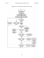
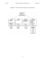
ECE 477
Digital Systems Senior Design Project
Spring 2009
Homework 9: Software Design Considerations
Due: Friday, March 27, at NOON
Team Code Name: Digi-iGuide Group No. 11
Team Member Completing This Homework: Kanchi Daiya
E-mail Address of Team Member: kdaiya @ purdue.edu
NOTE: This is the last in a series of four “design component” homework assignments, each of which is to be
completed by one team member. The body of the report should be 3-5 pages, not including this cover sheet,
references, attachments or appendices.
Evaluation:
SCORE
10
9
8
7
6
*
DESCRIPTION
Excellent – among the best papers submitted for this assignment. Very few
corrections needed for version submitted in Final Report.
Very good – all requirements aptly met. Minor additions/corrections needed for
version submitted in Final Report.
Good – all requirements considered and addressed. Several noteworthy
additions/corrections needed for version submitted in Final Report.
Average – all requirements basically met, but some revisions in content should be
made for the version submitted in the Final Report.
Marginal – all requirements met at a nominal level. Significant revisions in
content should be made for the version submitted in the Final Report.
Below the passing threshold – major revisions required to meet report
requirements at a nominal level. Revise and resubmit.
* Resubmissions are due within one week of the date of return, and will be awarded a score of
“6” provided all report requirements have been met at a nominal level.
Comments:
ECE 477
Digital Systems Senior Design Project
Spring 2009
1.0 Introduction
The Digi-iGuide is a hand-held device that displays the shortest walking path and points of interest to a
user on a LCD screen with the help of a GPS module. This device is designed to help visitors and
newcomers find their way around Purdue University in the most optimum manner. We calculate the
shortest path by implementing Dijkstra’s algorithm. Our application is a hybrid of interrupt driven and
program driven code. A microcontroller is used to poll through the status flags of peripherals and process
the respective requests. The peripherals include a LCD screen with touch capabilities to allow the user to
interface with the device, flash chips where the map, shortest path and points of interest data are stored. A
GPS module interfaces with the microcontroller over UART, we utilize Microchip’s USB stack to
implement USB such that we can send data to the flash chip via a microcontroller when the device is
connected to a PC.
2.0 Software Design Considerations
The PIC32 has two different addresses, a virtual address space and a physical address space,
mapped together with a Fixed Mapping Translation (FMT) unit. The virtual address space may
be partitioned into both user and kernel spaces, however the PIC32 data sheet only recommends
implementing the user mode for designs requiring multiple applications to run concurrently,
performing complex functionality. Our design will only need to perform relatively simple
functions sequentially, so it will run solely in kernel mode as the data sheet suggests. As a result,
RAM addresses are mapped from 0xA000000 - 0xA0007FFF. [1] Note that these numbers
correspond to the virtual address space, not the physical memory.
The Fixed Mapping Translation unit maps a portion of the address space to flash in a nearly
identical manner. The flash may be partitioned into user and kernel spaces in the same manner
as RAM, however since our application will be running in kernel mode for the reasons stated
earlier, we will not be partitioning the flash. [2] Since our program will be running in kernal
mode, we will be utilizing the KSEG1 portion of the virtual memory space.
-2-
Digital Systems Senior Design Project
ECE 477
Spring 2009
Figure 2.1 Fixed Memory Translation Unit
The registers that control peripherals are mapped to a block of memory that begins at
0xF800000.[1] We will be using the Microchip’s peripheral libraries to interface with external
interfaces, so there are very few if any memory-mapped I/O addresses that we will deal with
directly. Most of the interfacing will be accomplished through memory-mapped I/O, however
the peripheral libraries abstract this process largely with clever #define’s. As a result we are able
to write C code that looks high-level but compiles with no added overhead. For example,
sending a byte over UART 1 would be accomplished by writing a byte to U1TXREG register,
which is defined as a specific memory location, so the assembly would look something like this:
MOVB data,U1TXREG
-3-
Digital Systems Senior Design Project
ECE 477
Spring 2009
Using the UART peripheral library included with Microchip’s C32 compiler, we will send a byte
over the UART in the following manner (in C code):
WriteUART1(data);
So the library allows us to use easy-to-read syntax that appears to call a function, however the
function call is actually a #define, which will compile down to the identical machine code as the
assembly instruction.
#define WriteUART1(data)
U1TXREG = (data)
These libraries accomplish the tedious task of defining where in memory the peripheral control
registers are and providing intuitive interfaces to them. We will be using Microchip’s peripheral
code for both of our UARTs, SPI, and USB. Both UART modules will be operating with 8 data
bits, no parity, and one stop bit. The initialization will be as follows:
OpenUART1(UART_EN | UART_1STOPBIT,
UART_RX_ENABLE | UART_TX_ENABLE | UART_INT_RX_CHAR,
pbClk/16/DESIRED_BAUDRATE-1);
The initialization for each UART will be the same, however DESIRED_BAUDRATE will be
115200 for UART1 and 4800 for UART2. We will not be using any flow control. Our micro
controller will act as the master for the SPI. Our SPI chips can perform standard read operations
at 35 MHz, and all other operations at 75 MHz, so we will clock the SPI at 35 MHz [5]. The
PIC32 SPI module allows a frame mode
config = SPI_CON_MODE8|
// set SPI to send 8 bits at a time
SPI_CON_SMP|
// sample input at end of output(default)
SPI_CON_ON|
// SPI peripheral is enabled
SPI_CON_MSTEN;
// SPI configured as master
spi_channel = 1;
fpbClkDivider = 4;
// set clock to 35 MHz
SpiChnOpen(1, config, fpbClkDivider);
Peripheral
Pin Name
Pin Number
U1RX
51
U1TX
50
U2RX
31
U2TX
32
UART1
UART2
-4-
Digital Systems Senior Design Project
ECE 477
Peripheral
SPI
USB
Pin Name
Spring 2009
Pin Number
SCK2
4
SDI2
5
SDO2
6
RE3 (CS2)
63
RE4 (CS1)
64
VBUS
34
D+
37
D-
36
Table 2.1 Pin Designations
Microchip’s C32 compiler takes care of the majority of the memory details including the stack
and heap. The compiler only allocates space for a heap if the memory allocation functions are
used from the library. We do not need to use memory allocation, so our implementations will
not include a heap. We will have a limited number of global variables for information such as
flags, modes of operation (destination mapping mode, points of interest mode, PC mode, etc.),
and current location. Global variables and static values will be stored at the top of the RAM, and
the stack will begin at the bottom of RAM.
Code is stored in a specific section of flash and cached in during runtime. The compiler offers
the option to have RAM functions, or functions whose code is stored in RAM to allow for faster
execution, and these are stored at the very bottom of RAM below the stack. Since we are opting
to use lookup tables instead of lengthy algorithms to determine shortest path we will not need to
use RAM functions, and our stack will begin at the bottom of RAM. Once again, this is
managed by the compiler, and we will not need to know any more specifics.
We will be using a hybrid of interrupt driven and program driven application design. We will
have a number of “trigger” flags that will be set in various interrupts, and we will have a number
of “mode” flags that will be set while servicing the various “trigger” flags, and based on the
mode flags the polling loop will only perform specific functions. For instance, if input is
-5-
ECE 477
Digital Systems Senior Design Project
Spring 2009
received from the USB port, the ISR will set a “Computer mode” flag. Since the device will not
need to know its location while it is plugged into a computer, the polling loop will not update the
current GPS location. We chose this hybrid configuration since we will need to have interrupts
from user input, GPS input, etc., but the tasks we need to perform are to lengthy to include
entirely in the interrupts. Using the interrupt-flag hybrid design is also much more conducive to
configurations with multiple peripherals.
For debugging purposes we included a header on our PCB to connect our system to Microchip’s
ICD 2 debugger. The ICD 2 is a powerful debugging tool that not only programs the chip, but
also allows breakpoints, runtime memory mapping, and incremental program execution [1].
Additionally we will be using the PIC32 USB development board to get a jump start on
prototyping. We also included test points on the PCB for debugging the flash chips.
3.0 Software Design Narrative
From a big picture standpoint, our design will use a graph data structure with nodes
corresponding to specific pixels on a map image to display a shortest path to the user. The edges
of the graph will be weighted with the distance between the geographic points that the nodes
represent on the map. Instead of actually calculating the shortest path on the chip, all possible
shortest paths will be pre-computed on a PC, and then sent to the device via USB. The device
will store this information on the external flash chips and simply perform a table lookup when
the user inputs a destination.
The hierarchical arrangement of the code modules will begin with lightweight interrupt service
routines that will move information coming in over communications ports to circular FIFO
buffers since all of our peripherals deal with communications. Information will be pulled out of
these buffers using functions that act as drivers for the peripheral modules (Appendix B).
We will have a code module to interface with the GPS. The UART2 ISR will put location
information from the GPS device into a circular FIFO buffer. Since we will only be interested in
the most recent position, we will allow the ISR to just continually overwrite the buffer, allowing
enough space in the buffer so that at any given time we have a full set of GPS data. The GPS
-6-
ECE 477
Digital Systems Senior Design Project
Spring 2009
code module will have a GetCurrentPos function that will parse the data in the buffer into current
position information, and convert that into a node that corresponds to our graph. Currently, we
have the UART2 interface working such that the GPS module outputs the data string to a hyperterminal. We also have the code for the circular buffer set up, however integrating this with the
GPS data is required.
The code module that interfaces with the LCD module will include a SendImage function that
sends the map image to the LCD on start-up. The SendPath function will just send a string of
numbers that correspond to pixels on the image, and the LCD module will simply draw lines
between the specified pixels to show the user where the path is. The UART1 ISR will take userinput information sent from the LCD controller and set corresponding flags. The user input will
be short integer codings signifying that points of interest were requested or a destination has
been set, so the ISR will be able to handle parsing those commands and setting the appropriate
flag. The high speed UART interface has been implemented such that the LCD screen now
interfaces with the micro-controller displaying the example images that were provided to us with
the IDE.
The external flash module will have functions for getting/sending a map image, looking up a
path, and looking up points of interest. The get/send map image functions will only be executed
at start-up and when the device is connected to a PC. Since neither of these situations require
user-input or GPS information, these functions will disable interrupts from the UART
peripherals while running.
4.0 Summary
The Digi-iGuide’s software design will center around the application code of the microcontroller. The micro-controller will receive a map image, shortest path look-up table, and
points of interest information from a PC, and store this information on external flash chips. On
start-up the main program will start with a series of initialization functions that will power on the
LCD and external flash chips, load the map image from flash, and push that out to the LCD
controller. This initialization sequence and the subsequent main polling loop will interface with
the UARTs, SPI, and USB via peripheral modules. When the user inputs a destination it will
-7-
ECE 477
Digital Systems Senior Design Project
Spring 2009
look up the shortest path, and send the corresponding pixels that need to be displayed to the LCD
controller that eventually updates the image on the screen. After completing the user’s request
we poll for interrupt flags and assert or de-assert the corresponding “mode” flags, such that when
we loop back to check for mode flags, the values are updated. If the “connected to PC” mode is
set, we simply process the USB request. Thus making our software organization a hybrid of both
program-driven and interrupt-driven code.
-8-
ECE 477
Digital Systems Senior Design Project
Spring 2009
List of References
[1] Microchip, “MPLab ICD User’s Guide”, [Online Document]
http://ww1.microchip.com/downloads/en/DeviceDoc/51184d.pdf
[2] Microchip, “PIC32MX3XX/4XX Family Data Sheet”, [Online Document]
https://engineering.purdue.edu/477grp11/wpcontent/uploads/2009/02/pic32mx440f512h.pdf
[3] 4DGL, “LCD-32032-P1T Users Manual”, [Online Document]
https://engineering.purdue.edu/477grp11/wp-content/uploads/2009/02/ulcd-32032p1_users_manual_rev1_1.pdf
[4] GlobSat, “Product User Manual GPS Receiver Engine Board EM-406A”, [Online
Document] https://engineering.purdue.edu/477grp11/wp-content/uploads/2009/02/em406a-user-manual.pdf
[5] Winbond, “W25X16/16A/32/64 spiflash”, [Online Document]
https://engineering.purdue.edu/477grp11/wp-content/uploads/2009/02/w25x64vzeigflash.pdf
-9-
ECE 477
Digital Systems Senior Design Project
Appendix A: Flowchart/Pseudo-code for Main Program
-10-
Spring 2009
ECE 477
Digital Systems Senior Design Project
Appendix B: Hierarchical Block Diagram of Code Organization
-11-
Spring 2009