1
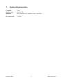
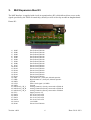
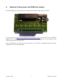
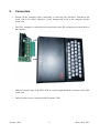
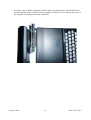
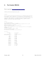
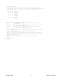
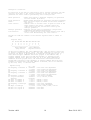
MrX Sound Board
for the ZX81 from Sinclair
“Manual for users and programmers”
www.eightbits.de
Version: v004
1
Date: 29.01.2012
CONTENT
1. System Requirements
.......... 4
2. MrX Sound Card
.......... 5
3. MrX Expansion Bus K3
.......... 6
4. Optional 3,5mm jacks and ZX96 bus diodes
.......... 7
5. Connection
.......... 8
6. Software
.......... 11
7. Programming
.......... 12
8. The Yamaha YM2149
.......... 15
Version: v004
2
Date: 29.01.2012
Disclaimer
This book is presented solely for educational and entertainment purposes. The author and publisher
are not offering it as legal, accounting, or other professional services advice. While best efforts have
been used in preparing this book, the author and publisher make no representations or warranties of
any kind and assume no liabilities of any kind with respect to the accuracy or completeness of the
contents and specifically disclaim any implied warranties of merchantability or fitness of use for a
particular purpose. Neither the author nor the publisher shall be held liable or responsible to any
person or entity with respect to any loss or incidental or consequential damages caused, or alleged
to have been caused, directly or indirectly, by the information or programs contained herein. No
warranty may be created or extended by sales representatives or written sales materials. Every
company is different and the advice and strategies contained herein may not be suitable for your
situation. You should seek the services of a competent professional before beginning any actions
described in this manual.
Version: v004
3
Date: 29.01.2012
1.
System Requirements
Computer:
Manufacturer:
Amplifier:
ZX81
Sinclair, UK
active amplifier (PC-amplifier) with 3,5mm jack
Recommended:
16k Ram
Version: v004
4
Date: 29.01.2012
2.
MrX Sound Card
A) 3,5mm jack. Connect the amplifier here.
B) Port connector.
C) 30 pin expansion bus K3 (see next chapter)
D) Through port connector.
Version: v004
5
Date: 29.01.2012
3.
MrX Expansion Bus K3
The MrX Interface is supplied with a built in expansion bus (K3) which allows direct access to the
signals provided by the YM2149 sound chip, should you wish to develop an add-on daughterboard.
Pinout K3:
1)
2)
3)
4)
5)
6)
7)
8)
9)
10)
11)
12)
13)
14)
15)
16)
17)
18)
19)
20)
21)
22)
23)
24)
25)
26)
27)
28)
29)
30)
IOB7
IOB6
IOB5
IOB4
IOB3
IOB2
IOB1
IOB0
IOA7
IOA6
IOA5
IOA4
IOA3
IOA2
IOA1
CHL
CHR
GND
/CLK
GND
ANALOG_CH_C
ANALOG_CH_B
ANALOG_CH_A
VCC
GAL1
GAL2
GAL3
GAL4
clock/2
IOA0
Version: v004
Port B from YM2149
Port B from YM2149
Port B from YM2149
Port B from YM2149
Port B from YM2149
Port B from YM2149
Port B from YM2149
Port B from YM2149
Port A from YM2149
Port A from YM2149
Port A from YM2149
Port A from YM2149
Port A from YM2149
Port A from YM2149
Port A from YM2149
Left channel of 3,5mm jack, behind capacitor
Right channel of 3,5mm jack, behind capacitor
Ground
ZX81 clock signal 3,25 MHz
Ground
Analog Channel C directly connected to YM2149
Analog Channel B directly connected to YM2149
Analog Channel A directly connected to YM2149
Supply current +5V
Pin 15 of GAL 16V8
Pin 14 of GAL 16V8
Pin 13 of GAL 16V8
Pin 12 of GAL 16V8
1,625 MHz
Port A from YM2149
6
Date: 29.01.2012
4.
Optional 3,5mm jacks and ZX96 bus diodes
If needed additional 3,5mm jacks can be soldered on the MrX sound card on J1 and J2.
For the ZX96 bus (http://www.fischerkai.de/zxteam/treib_e.htm) a diode DX1 for the /BUSCS
signal has to be soldered and the port connector has to be exchanged by a VG64 connector. The
VG64 connector uses all pins of K2.
Note: The ZX96 bus is only used by some freaks, if your ZX81 is equipped with the same the
original MrX won't fit mechanically.
Version: v004
7
Date: 29.01.2012
5.
Connection
•
Switch off the computer before connecting or removing any interfaces. Disconnect the
power lead to be certain! Otherwise, severe damage may occur to the computer and the
sound card.
•
The ZX81 computer is connected to the sound card via the ZX expansion port on the back of
the computer.
•
Make sure that the pins of the ZX81 PCB are exactly aligned with the connector of the MrX
sound card.
•
Don't use brute force to connect the MrX with the ZX81.
Version: v004
8
Date: 29.01.2012
•
The PC speaker (with integrated amplifier) has to be connected with the 3,5mm stereo jack.
Version: v004
9
Date: 29.01.2012
•
If needed, connect further equipment. NOTE: Make sure that the pins of the MrX PCB are
exactly aligned with the connector of the equipment. Otherwise severe damage may occur to
the computer, the equipment and the sound card.
Version: v004
10
Date: 29.01.2012
6.
Software
This manual and the software for the MrX sound card is provided at http://www.eightbits.de/ in the
download section.
manual.pdf
AY-Demo
Basic-Demo
Demon-Demo
Games
PT3-Player
Pink-Panther
ZON-X-Manual
→ This manual
→ Sound-Demo
→ Original Basic Demos from the ZON-X Manual
→ Dancing Demon Demo
→ 2 Games from Brasilian TK85
→ Player, plays PT3-files
→ Music demo
→ HTML document original zonx manual
Concerning the PT3-Player, PT3-files have to be converted to wav-files according the instructions
in the ZX81 forum „http://www.rwapservices.co.uk/ZX80_ZX81/forums/aye-ayet528s170.html#p4919 “.
Version: v004
11
Date: 29.01.2012
7.
Programming
The MrX is compatible with the original ZON-X sound card.
Addresses:
The MrX Interface responds to data placed in the following addresses:
Latch
Data
Comment
0xDF
0xCF
0xCF
0xDF
0x0F
0x1F
0x0F
0x1F
modified ZON-X
original ZON-X
from ZON-X user manual
additional combination
See chapter “8. The Yamaha YM2149” for further explanation about “Latch” (register address
latch) and “Data” (write mode).
Examples in assembler
Simple Sound:
;
LATCH:
LATCH:
DTAX:
DTAX:
;
equ
equ
equ
equ
$DF
$CF
$0F
$1F
xxx:
LD
out
LD
out
A,7
(LATCH),A
A,$C0
(DTAX),A
LD
out
LD
out
A,$08
(LATCH),A
A,15
(DTAX),A
looop:
LD
out
LD
out
ret
A,0
(LATCH),A
A,70
(DTAX),A
Version: v004
12
Date: 29.01.2012
Output on port A:
;
DTAX: equ $0F
DTAX: equ $1F
LATCH: equ $CF
;
LATCH:
equ $DF
xxx:
LD A,7
out (LATCH),A
LD A,$C0
;---> set port A and B as output
out (DTAX),A
looop:
LD A,14
out (LATCH),A
LD A,$00
out (DTAX),A ; set port A to 0
LD HL,(DFILE)
INC HL
LD (HL),_O
INC HL
LD (HL),_F
INC HL
LD (HL),_F
LD BC,100
CALL $0F35
LD A,14
out (LATCH),A
LD A,$FF
out (DTAX),A
LD HL,(DFILE)
INC HL
LD (HL),_O
INC HL
LD (HL),_N
INC HL
LD (HL),__
; set all bits of port A to 1 (high)
LD BC,100
CALL $0F35
jp
looop
Version: v004
13
Date: 29.01.2012
Reading from port A:
;
;
DTAX: equ $0F
DTAX: equ $1F
LATCH: equ $CF
LATCH: equ $DF
xxx:
LD A,7
out (LATCH),A
LD A,$00
out (DTAX),A
;--> set port A & B to Input
looop:
LD A,14
out (LATCH),A
in a,(LATCH)
and a,$3F
;Port A (register No. 14) is read
LD HL,(DFILE)
INC HL
LD (HL),A
;Print the port content to the screen
jp
looop
Version: v004
14
Date: 29.01.2012
8.
The Yamaha YM2149
This is a copy from “http://www.atari-forum.com/wiki/ “.
Software-Controlled Sound Generator (SSG)
----------------------------------------Overview
The SSG (Software-Controlled Sound Generator) is an NMOS-LSI device designed
to be capable of music generation. It only requires the microprocessor or
microcomputer (CPU) to initialize its register array, thus reducing the load
on the CPU. Music generation is carried out by the three sequence square wave
generator, noise generator, and envelope generator according to the set
parameters. This allows for the generation of music, special effects,
warnings, and various other types of sounds.
Features
5V single power supply
Easy connection to 8 bit or 16 bit CPU
Simple connection to external system through 2 sequence 8 bit I/O port
Wide voicing range of 8 octaves
Smooth attenuation by 5 bit envelope generator
Built-in 5 bit D/A convertor
Input of double frequency clock can be handled by built-in clock frequency
divider
TTL compatible level
Low power consumption (typical 125mW)
40 pin plastic DIL package
Pin compatible with AY-3-8910 manufactured by GI
Pin Layout
Vss(GND) 1
N.C 2
Analog Channel B 3
Analog Channel A 4
N.C 5
IOB7 6
IOB6 7
IOB5 8
IOB4 9
IOB3 10
IOB2 11
IOB1 12
IOB0 13
IOA7 14
IOA6 15
IOA5 16
IOA4 17
IOA3 18
IOA2 19
IOA1 20
Version: v004
40
39
38
37
36
35
34
33
32
31
30
29
28
27
26
25
24
23
22
21
Vcc(+5V)
Test1
Analog Channel C
DA0
DA1
DA2
DA3
DA4
DA5
DA6
DA7
BC1
BC2
BDIR
SEL
A8
A9
RESET
CLOCK
IOA0
15
Date: 29.01.2012
Block diagram
A9 A8
BDIR BC2 BC1
DA7~DA0
o o
o
o
o
|
| |
|
|
|
|
| |
|
|
|
|
| |
--- Bus Control ---o Bidirectional
-----o I/O Port A <=> IOA7~IOA0
| |
|
Decoder
o--buffer
|
| |
|
o
|
| |
|
|
|
| |
o
o
|
Register Addr --o Address --o Register o-------|
Latch
Decoder
Array
-----o I/O Port B <=> IOB7~IOB0
o
|
-------------------------------------|
|
|
|
|
o
o
|
o
o
Noise
Music
| Envelope
Level
Frequency
Generator Generator | Generator --o Control o----- divider ---o CLOCK
|
|
|
|
master
|
|
o
|
|
clock
|
-------o Mixer o-|
---------o SEL
|
|
|
|
o
|
D/A Convertor o-----------------|
|
|
|
|
|
Analog Channel
o
o
o
A
B
C
Description of pins
1. DA7 ~ DA0
This is an 8 bit bidirectional data bus which is used for moving data and
addresses between the SSG and CPU. In the read and write modes, DA7 ~ DA0
corresponds to B7 ~ B0 of the register array. In the address mode, DA3 ~ DA0
is used for the register address, and DA7 ~ DA4 is used together with A9 and
A8 for the upper address.
2. A8 and A9
These are the upper address input pins. A8 has pullup resistance while A9
has pulldown resistance. When the voltage level at A8 while the level at A9
and DA7 ~ DA4 is low, the address mode is selected allowing for the fetching
of a register address. Connect A8 and A9 to +5V and ground respectively when
not in use.
3. RESET
Reset is effective when the voltage level is low, and the contents of all
registers in the array are reset to '0'. This pin has pullup resistance.
4. CLOCK
Supplies the master clock to the sound generator and envelope generator. This
is equipped with a 1/2 frequency divider which allows for the use of a
frequency which is 1/2 of the input clock, as the master clock.
5. SEL
When SEL is driven to the high level, the input clock is taken as the master
clock. When the voltage level of SEL is low, the input clock is divided by 2
to obtain the master clock. This pin has pullup resistance, allowing for
full pin compatibility with the AY-3-8910 manufactured by AI, when this pin
is not connected to anything.
Version: v004
16
Date: 29.01.2012
6. BDIR,BC1 and BC2
Controls the external bus (DA7 ~ DA0) and internal bus of the SSG. The
following four modes can be set by the bus control decoder. The bus control
is redundant, control is possible even when BC5 is connected to +5V.
BDIR BC2 BC1
0
0
0
0
0
1
0
1
0
0
1
1
1
0
0
1
0
1
1
1
0
1
1
1
Mode
Inactive
Address
Inactive
Read
Address
Inactive
Write
Address
Inactive mode: DA7 ~ DA0 has high impedance.
Address mode: DA7 ~ DA0 set to input mode, and address is fetched from
register array.
Write mode:
DA7 ~ DA0 set to input mode, and data is written to register
currently being addressed.
Read mode:
DA7 ~ DA0 set to output mode, and contents of register
currently being addressed are output.
7. ANALOG CHANNEL A,B,C
Each of the three channels is equipped with a D/A convertor which converts
the calculated digital values to analog signals for output.
8. IOA7 ~ IOA0, IOB7 ~ IOB0
These are two 8 bit I/O ports. These ports allow the SSG to be placed
between an external system and the CPU for the transfer of data. These pins
have pullup resistance.
9. TEST1
Output pin for testing the device. Do not connect to anything.
10. Vcc
+5V power pin.
11. Vss
Ground pin.
Version: v004
17
Date: 29.01.2012
Description of funtions
All functions of the SSG are controlled by the 16 internal registers. The CPU
need only write data to the internal registers of the SSG. The SSG itself
generates the sound. Sound is generated by the following blocks:
Music generator:
Noise generator:
Mixer:
Square waves having a different frequency are generated
for each channel (A,B and C)
Pseudo-random waveforms are generated (variable frequency)
Music and noise output are mixed for the three channels
(A,B and C)
Constant level or variable level is given for each of the
three channels (A,B and C). Constant levels are
controlled by the CPU, and variable levels by the
envelope generator.
Generates various types of attenuation (single burst
attenuated and repeated attenuation)
Sound is output on each of the three channels (A,B and C)
at the level determined by the level control.
Level control:
Envelope generator:
D/A convertor:
The CPU can read the contents of the internal registers with no effect on
sound.
Register Array
A9 A8 DA7 DA6 DA5 DA4 DA3 DA2 DA1 DA0
0
1
0
0
0
0
0
0
0
0
0
1
0
0
0
0
1
1
1
1
\______________________/\_____________/
Upper addresses
Lower addresses
(chip select)
(register select)
Of the ten bit address, the lower addresses DA3 ~ DA0 are used to select the
16 internal registers(register array). The upper addresses are used for chip
selection. A9 and A8 is programmed to 01 while DA7 through DA4 are set to
0000. When the upper addresses match this program in the address mode, a
register address (lower four bits DA3 through DA0) is fetched from the
register address latch. When the value set is in the upper addresses is
different from the program value, the bidirectional bus formed from DA7
through DA0 is driven to high impedance. A register address which has been
fetched is retained until the next address is fetched, and is not affected
by the read, write, or inactive mode.
Register Array
R0
R1
R2
R3
R4
R5
R6
R7
Frequency of Channel A
Frequency of Channel B
Frequency of Channel C
Frequency of Noise
I/O port and mixer
settings
Level of channel A
Level of channel B
Level of channel C
Frequency of envelope
R8
R9
RA
RB
RC
RD Shape of envelope
RE Data of I/O port A
RF Data of I/O port B
Version: v004
B7....B0
00000000
----0000
00000000
----0000
00000000
----0000
---00000
iinnnttt
bacbacba
---mllll
---mllll
---mllll
00000000
00000000
----cath
00000000
00000000
8 bit fine tone adjustment
4 bit rough tone adjustment
8 bit fine tone adjustment
4 bit rough tone adjustment
8 bit fine tone adjustment
4 bit rough tone adjustment
5 bit noise frequency
i-I/O, n-Noise, t-Tone
m-Mode, l-Level
m-Mode, l-Level
m-Mode, l-Level
8 bit fine adjustment
8 bit rough adjustment
c-Cont, a-Att, t-Alt, h-Hold
8 bit data
8 bit data
18
Date: 29.01.2012
(1) Setting of music frequency (controlled by registers R0 ~ R5)
The frequencies of the square wave generated by the music generators for the
three channels (A,B and C) are controlled by registers R0 through R5. R0 and
R1 control channel A, R2 and R3 are used for channel B, and R4 and R5 control
channel C. The oscillation frequency fT is obtained in the following manner
from the value of the register TP(decimal).
fT = fMaster
------16TP
fMaster is the frequency of the master clock (this is the input click
frequency when
SEL is high, and 1/2 of this frequency when low).
Rough tone adjustment
register
R1
R3
R5
Channel
A
B
C
Fine tone adjustment
register
R0
R2
R4
B7 B6 B5 B4 B3 B2 B1 B0
B7 B6 B5 B4 B3 B2 B1 B0
\---------/|
\
/
Not used |
\
/
|
|
TP11 TP10 TP9 TP8 TP7 TP6 TP5 TP4 TP3 TP2 TP1 TP0
12 bit oscillation frequency setting value (TP)
(2) Setting of noise generator (controlled by register R6)
The noise frequency fN is obtained from the register value NP(decimal) in the
following manner.
fN = fMaster
------16NP
(fMaster if the frequency of the master clock)
Noise frequency register R6
B7 B6 B5 B4 B3 B2 B1 B0
\------/|
\
Not used|
\
|
|
NP4 NP3 NP2 NP1 NP0
5 bit noise frequency setting value (NP)
(3) Settings of mixer and I/O ports (controlled by register R7)
The mixer is used to combine music and noise components. The combination is
determined by bits B5 ~ B0 of register R7. Sound is output when a '0' is
written to the register. Thus, when both the noise and tone are '0', the
output is combined by the mixer. When the noise is '0' and the tone is '1',
only the noise signal is output. When the noise is '1' and the tone is '0',
music (square wave) is output. Nothing is output when both the noise and tone
are '1'. Selection of input/output for the I/O ports is determined by bits B7
and B6 of register R7. Input is selected when '0' is written to the register
bits.
I/O port and mixer setting register R7
B7 B6 B5 B4 B3 B2 B1 B0
/
/|
|\
\
/
/ |
| \
\
I/O
Noise
Tone
B
A
C
B
A
C
B
A
(Input is selected for I/O port when '0', and noise or tone can be output
when '0')
Version: v004
19
Date: 29.01.2012
(4) Level control (controlled by R8 ~ RA)
The audio level output from the D/A convertors for the three channels (A,B
and C) is adjusted by registers R8, R9 and RA.
Level setting registers
R8
R9
RA
Channel
A
B
C
B7 B6 B5 B4 B3 B2 B1 B0
\------/| |\
\
Not used| | \
\
| |
\
\
M
L3 L2 L1 L0
Mode
4 bit level selection
Mode M selects whether the level is fixed (when M=0) or variable (M=1). When
M=0, level is determined from one of 16 by level selection signals L3,L2,L1
and L0 which compromise the lower four bits. When M=1, the level is determined
by the 5 bit output of E4,E3,E2,E1 and E0 of the envelope generator of the
SSG. (This level is variable as E4 ~ E0 change over time)
(5) Setting of envelope frequency (controlled by R8 and RC)
Thus, the envelope repetition frequency fE is obtained as follows from the
envelope setting period value EP (decimal):
fE = fMaster
------256EP
(fMaster if the frequency of the master clock)
Envelope rough adjustment register RC Envelope fine adjustment register RB
B7 B6 B5 B4 B3 B2 B1 B0
B7 B6 B5 B4 B3 B2 B1 B0
/
\
/
\
/
\
/
\
/
|
\
EP15 EP14 EP13 EP12 EP11 EP10 EP9 EP8 EP7 EP6 EP5 EP4 EP3 EP2 EP1 EP0
16 bit envelope period setting value (EP)
The period of the actual frequency fEA used for the envelope generated is
1/32 of the envelope repetition period (1/fE).
(6) Envelope shape control (controlled by RD)
The envelope generator counts the envelope clock fEA 32 times for each
envelope pattern cycle. The envelope level is determined by the 5 bit output
(E4 ~ E0) of the counter. The shape of the envelope is created by increasing,
decreasing, stopping, or repeating this counter. The shape is controlled by
bits B3 ~ B0 of the register RD.
Envelope shape control register RD
B7 B6 B5 B4 B3 B2 B1 B0
\----------/ | | | |
Not used
| | | --- Hold
| | ------ Alt
| --------- Att
------------ Cont
Envelope shape control signals
Version: v004
20
Date: 29.01.2012
The envelope can take the shapes shown below according to combinations of the
CONT, ATT, ALT and HOLD signals.
B3 B2 B1
B0
CONT ATT ALT HOLD
0
0
x
x \
\--------------------0
1
x
x
/|
/ |--------------------
1
0
0
0
\ |\ |\ |\ |\ |\ |\ |\
\| \| \| \| \| \| \| \
1
0
0
1
\
1
0
1
0
\
\--------------------/\
/\
\/
/\
\/
/\
\/
/\
\/
/
\/
\/
1
0
1
1
\ |-------------------\|
1
1
0
0
/| /| /| /| /| /| /| /
/ |/ |/ |/ |/ |/ |/ |/
1
1
0
1
1
1
1
0
/---------------------
/
/\
/
1
1
1
1
/\
\/
/\
\/
/\
\/
/\
\/
/\
\/
\
/|
/ |--------------------
NOTE - The writing to register RD will reset the envelope frequency clock
Version: v004
21
Date: 29.01.2012