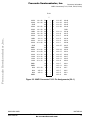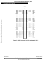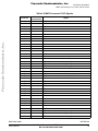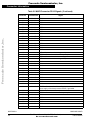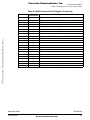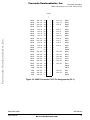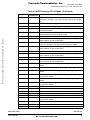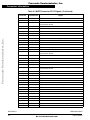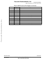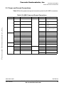
1
Freescale Semiconductor, Inc. Freescale Semiconductor, Inc... MMCLAB01 Logic Analyzer Board User’s Manual Motorola reserves the right to make changes without further notice to any products herein to improve reliability, function or design. Motorola does not assume any liability arising out of the application or use of any product or circuit described herein; neither does it convey any license under its patent rights nor the rights of others. Motorola products are not designed, intended, or authorized for use as components in systems intended for surgical implant into the body, or other applications intended to support or sustain life, or for any other application in which the failure of the Motorola product could create a situation where personal injury or death may occur. Should Buyer purchase or use Motorola products for any such unintended or unauthorized application, Buyer shall indemnify and hold Motorola and its officers, employees, subsidiaries, affiliates, and distributors harmless against all claims, costs, damages, and expenses, and reasonable attorney fees arising out of, directly or indirectly, any claim of personal injury or death associated with such unintended or unauthorized use, even if such claim alleges that Motorola was negligent regarding the design or manufacture of the part. Motorola and are registered trademarks of Motorola, Inc. Motorola, Inc. is an Equal Opportunity/Affirmative Action Employer. The M•CORE name and logotype and the OnCE name are trademarks of Motorola, Inc. © Motorola, Inc. 1999 For More Information On This Product, Go to: www.freescale.com Freescale Semiconductor, Inc. MMCLAB01UM/D CAUTION: ESD Protection Freescale Semiconductor, Inc... M•CORE development systems include open-construction printed circuit boards that contain static-sensitive components. These boards are subject to damage from electrostatic discharge (ESD). To prevent such damage, you must use static-safe work surfaces and grounding straps, as defined in ANSI/EOS/ESD S6.1 and ANSI/EOS/ESD S4.1. All handling of these boards must be in accordance with ANSI/EAI 625. MOTOROLA 2 MMCLAB01UM/D For More Information On This Product, Go to: www.freescale.com Reference Manual Freescale Semiconductor, Inc. Table of Contents Freescale Semiconductor, Inc... Section 1 Introduction 1.1 1.2 1.3 1.4 1.5 LAB01 Features . . . . . . . . . . . . . . . . . . . . . . . . . . . . . . . . . . . . . . . . . . 9 System and User Requirements . . . . . . . . . . . . . . . . . . . . . . . . . . . . . . 9 LAB01 Layout . . . . . . . . . . . . . . . . . . . . . . . . . . . . . . . . . . . . . . . . . . . 10 Using the Breadboard and Spare Areas . . . . . . . . . . . . . . . . . . . . . . . 12 Connecting the LAB01 . . . . . . . . . . . . . . . . . . . . . . . . . . . . . . . . . . . . 13 Section 2 Connector Information 2.1 2.2 2.3 MAPI Connectors (P1/J1, P2/J2, P3/J3, P4/J4) . . . . . . . . . . . . . . . . . 15 Logic Analyzer Connectors (J5 through J16) . . . . . . . . . . . . . . . . . . . 40 Power and Ground Connections. . . . . . . . . . . . . . . . . . . . . . . . . . . . . 49 Index Revision History MMCLAB01UM/D User’s Manual MOTOROLA For More Information On This Product, Go to: www.freescale.com 3 Freescale Semiconductor, Inc. Freescale Semiconductor, Inc... Table of Contents MOTOROLA 4 MMCLAB01UM/D For More Information On This Product, Go to: www.freescale.com User’s Manual Freescale Semiconductor, Inc. Freescale Semiconductor, Inc... List of Figures Figure 1-1 Figure 2-1 Figure 2-2 Figure 2-3 Figure 2-4 Figure 2-5 Figure 2-6 Figure 2-7 MMCLAB01 Logic Analyzer Board. . . . . . . . . . . . . . . . . . . . . . 11 MAPI Connector P1/J1 Pin Assignments (100–51) . . . . . . . . . 16 MAPI Connector P1/J1 Pin Assignments (50–1) . . . . . . . . . . . 17 MAPI Connector P2/J2 Pin Assignments (100–51) . . . . . . . . . 21 MAPI Connector P2/J2 Pin Assignments (50–1) . . . . . . . . . . . 22 MAPI Connector P3/J3 Pin Assignments (100–51) . . . . . . . . . 26 MAPI Connector P3/J3 Pin Assignments (50–1) . . . . . . . . . . . 27 MAPI Connector P4/J4 Pin Assignments (100–51) . . . . . . . . . 32 Figure 2-8 Figure 2-9 Figure 2-10 Figure 2-11 Figure 2-12 Figure 2-13 Figure 2-14 Figure 2-15 Figure 2-16 Figure 2-17 Figure 2-18 Figure 2-19 Figure 2-20 MAPI Connector P4/J4 Pin Assignments (50–1) . . . . . . . . . . . 33 Connector J5 Pin Assignments . . . . . . . . . . . . . . . . . . . . . . . . 40 Connector J6 Pin Assignments . . . . . . . . . . . . . . . . . . . . . . . . 40 Connector J7 Pin Assignments . . . . . . . . . . . . . . . . . . . . . . . . 41 Connector J8 Pin Assignments . . . . . . . . . . . . . . . . . . . . . . . . 41 Connector J9 Pin Assignments . . . . . . . . . . . . . . . . . . . . . . . . 42 Connector J10 Pin Assignments . . . . . . . . . . . . . . . . . . . . . . . 43 Connector J11 Pin Assignments . . . . . . . . . . . . . . . . . . . . . . . 44 Connector J12 Pin Assignments . . . . . . . . . . . . . . . . . . . . . . . 45 Connector J13 Pin Assignments . . . . . . . . . . . . . . . . . . . . . . . 46 Connector J14 Pin Assignments . . . . . . . . . . . . . . . . . . . . . . . 47 Connector J15 Pin Assignments . . . . . . . . . . . . . . . . . . . . . . . 47 Connector J16 Pin Assignments . . . . . . . . . . . . . . . . . . . . . . . 48 MMCLAB01UM/D User’s Manual MOTOROLA For More Information On This Product, Go to: www.freescale.com 5 Freescale Semiconductor, Inc. Freescale Semiconductor, Inc... List of Figures MOTOROLA 6 MMCLAB01UM/D For More Information On This Product, Go to: www.freescale.com User’s Manual Freescale Semiconductor, Inc. List of Tables LAB01 Design Specifications . . . . . . . . . . . . . . . . . . . . . . . . . . . 12 MAPI Connector P1/J1 Signals . . . . . . . . . . . . . . . . . . . . . . . . 18 MAPI Connector P2/J2 Signals . . . . . . . . . . . . . . . . . . . . . . . . 23 MAPI Connector P3/J3 Signals . . . . . . . . . . . . . . . . . . . . . . . . 28 MAPI Connector P4/J4 Signals . . . . . . . . . . . . . . . . . . . . . . . . 34 LAB01 Power and Ground Connections . . . . . . . . . . . . . . . . . . 49 Freescale Semiconductor, Inc... Table 1-1 Table 2-1 Table 2-2 Table 2-3 Table 2-4 Table 2-5 MMCLAB01UM/D User’s Manual MOTOROLA For More Information On This Product, Go to: www.freescale.com 7 Freescale Semiconductor, Inc. Freescale Semiconductor, Inc... List of Tables MOTOROLA 8 MMCLAB01UM/D For More Information On This Product, Go to: www.freescale.com User’s Manual Freescale Semiconductor, Inc. Section 1 Introduction Freescale Semiconductor, Inc... This user’s manual explains connection and operation information for the MMCLAB01 Logic Analyzer Board (LAB01), a development tool of Motorola’s M•CORE™ family. You may use the LAB01 with a compatible host processor board or other circuit boards that connect via a MAPI400 ring. The MAPI400 ring is a group of four high-density connectors. The LAB01 brings out signals from the pins of these MAPI connectors to dual-row pin headers that you can use as connection points for prototype circuits or test-equipment probes. The dual-row pin headers have 0.1-inch (0.045mm) spacing; many also connect to solder pads. Additionally, the board has a breadboard area and spare pads, making it easy for you to add your own components to circuits. 1.1 LAB01 Features The LAB01 features: • Four 2-by-10-pin connectors, compatible with the cable termination adapter (part HP 01650-63203) of a Hewlett-Packard logic analyzer. Optionally, you can use individual connections to pins of these connectors. • Seven 2-by-20-pin connectors, and one additional 2-by-10-pin connector, giving you access to MAPI-ring signals via individual pin connections. • A 15.75-square-inch (101.6-square-centimeter) through-hole breadboard area, for easy addition of custom components to your design. Adjacent to this breadboard area are convenient connection points for ground, host power, and 5-volt power. • Eight spare pad strips for easy addition of surface-mount custom components to your design. There are two strips in each of four sizes: 25.6 mils pitch and 250 mils width, 50 mils pitch and 220 mils width, 25.6 mils pitch and 260 mils width, and 50 mils pitch and 380 mils width. 1.2 System and User Requirements To use the LAB01, you need a compatible host processor board, such as the Motorola MMCCMB1200 Controller and Memory Board, or some other MAPI-compliant tool. The host processor board plugs onto the LAB01 MAPI400 ring, providing power and data signals to the LAB01. MMCLAB01UM/D User’s Manual MOTOROLA For More Information On This Product, Go to: www.freescale.com 9 Freescale Semiconductor, Inc. Introduction The LAB01 has no computer or software requirements of its own. Your host processor determines what hardware and software you need for your development activities. If your host processor board is MAPI400-compatible, the signal labels of LAB01 dual-row pin headers will be accurate. CAUTION: A non-compatible host processor board could short out power and ground connections if plugged onto the LAB01. 1.3 LAB01 Layout Freescale Semiconductor, Inc... Figure 1-1 shows the layout of the LAB01. Connectors P1 through P4 are the MAPI connectors. (The corresponding MAPI connectors on the bottom of the board are J1 through J4.) Connectors J5 through J8 are the HP-compatible logic analyzer connectors. Connectors J9 through J16 make available many other signals of the MAPI ring. The through-hole breadboard area is at the opposite end of the board from the MAPI ring. Ground connection points flank the breadboard area. VDDH (host voltage) connection points run along the edge of the board; VDD5V (5-volt) connection points run along the opposite edge of the breadboard area. The spare pads, for surface-mount components, are near the center of the LAB01. Note the labeling conventions for the LAB01’s dual-row pin headers: • • • • • • M designations denote a MAPI connector and pin. For example, M13 means that the pin brings out the signal from connector P1 (or J1), pin 3. M281 means that the pin brings out the signal from connector P2 (or J2), pin 81. Other designations follow the MAPI-specification signal names, as does connector J10, pin 1, labelled EXTAL. This is the EXTAL signal of MAPI connectors P3/J3, pin 93. Many LAB01 designations are shortened versions of the MAPI-specification signal names. An example is connector J7, pin 3, labeled CLKOT. This is the CLKOUT signal of MAPI connectors P4/J4, pin 95. (Note that the LAB01 uses an asterisk, not the specification’s _b suffix, to indicate active-low signals.) GND, GND1, GND2, GND3, GND4, VDD5V, and VDDH denote ground and power pin. These pins connect to LAB01 planes, rather than specific MAPI pins. Thus, all pins labeled VDDH, whether of the dual-row headers or the MAPI connectors, connect to the host voltage plane. OPEN denotes pins that have no assigned signals. You may use these pins for any purpose you like. NC (or no label) denotes pins that should not have any connections. MOTOROLA 10 MMCLAB01UM/D For More Information On This Product, Go to: www.freescale.com User’s Manual Freescale Semiconductor, Inc. Introduction LAB01 Layout NOTE: Connecting any signal to an NC or unlabeled pin could impair the logic-analyzer usefulness of the connector. VDDH GND GND J6 J5 Breadboard Area J8 Freescale Semiconductor, Inc... J7 GND GND VDD5V J9 J10 J12 Spare Pad Sites J11 P4 J14 J13 P1 P3 J16 J15 P2 Figure 1-1 MMCLAB01 Logic Analyzer Board MMCLAB01UM/D User’s Manual MOTOROLA For More Information On This Product, Go to: www.freescale.com 11 Freescale Semiconductor, Inc. Introduction Table 1-1 lists LAB01 specifications. Table 1-1 LAB01 Design Specifications1 Specifications1 Characteristic Operating temperature 0° to 40° C Storage temperature -40° to +85° C Relative humidity 0 to 90% (non-condensing) Power Requirements None Dimensions 9.65 x 13.0 inches (245.1 x 330.2 mm) Freescale Semiconductor, Inc... NOTES: 1. These specifications conform to the product design; they have not been tested with actual boards. 1.4 Using the Breadboard and Spare Areas The LAB01’s breadboard area lets you add your own components to the board. Merely insert the component’s leads through holes in the board, then solder the leads in place. Run appropriate wires from the new component to board power and ground locations. Note that the top row of breadboard-area holes are host-voltage (VDDH) sources, the bottom row of holes are +5-volt (VDD5V) sources, and the columns of holes at either side are ground connections. The LAB01’s spare pads let you add your own surface-mount components to the board. The four pad sizes are: • 25.6 mils pitch by 250 mils width, • 50 mils pitch by 220 mils width, • 25.6 mils pitch by 260 mils width, and • 50 mils pitch by 380 mils width. Solder the component’s leads to the appropriate solder bars to hold the component in position. Then run appropriate wires from the small adjacent through-holes to board power, ground, and signal locations. NOTE: If you do add components in the breadboard or spare-pad areas, make sure that their current draw does not exceed the power supply limits of your host processor board. MOTOROLA 12 MMCLAB01UM/D For More Information On This Product, Go to: www.freescale.com User’s Manual Freescale Semiconductor, Inc. Introduction Connecting the LAB01 1.5 Connecting the LAB01 In order to use your LAB01, you must connect it to a compatible host processor board. To do so, place the LAB01 on your work surface. Note the position of the silk-screen right-triangle marking, at the ends of MAPI connectors P1 and P2. Hold the host board directly above the LAB01. Orient the host board so that its MAPI connectors and right-triangle marking are directly above their LAB01 counterparts. Freescale Semiconductor, Inc... Press the host board down onto the LAB01, so that host-board MAPI connectors J1 through J4 (on the bottom of the board) connect to the LAB01’s corresponding MAPI connectors, P1 through P4. NOTE: The rows of large holes accommodate legs and compatible boards. The holes along the board’s edges and down the center line, are for the metal legs that hold the LAB01 an inch or so above your work surface. The intermediate holes let you bolt a compatible board (of any of three sizes) to the LAB01. An appropriate hardware kit comes with your LAB01. Consult the host-board user’s manual for instructions about making cable connections. MMCLAB01UM/D User’s Manual MOTOROLA For More Information On This Product, Go to: www.freescale.com 13 Freescale Semiconductor, Inc. Freescale Semiconductor, Inc... Introduction MOTOROLA 14 MMCLAB01UM/D For More Information On This Product, Go to: www.freescale.com User’s Manual Freescale Semiconductor, Inc. Section 2 Connector Information This section consists of pin assignments and signal descriptions for LAB01 connectors. A table of power and ground connections ends this section. Freescale Semiconductor, Inc... 2.1 MAPI Connectors (P1/J1, P2/J2, P3/J3, P4/J4) Connectors P1 through P4, all 2-by-50-pin connectors, are the LAB01 MAPI connectors. (Connectors J1 through J4, on the bottom of the LAB01, have the same pin assignments.) The diagram below shows the orientation of these connectors. Figure 2-1 through Figure 2-8, and Table 2-1 through Table 2-4, give the pin assignments and signal descriptions for these connectors. 100 100 1 P4 P1 1 100 P3 P2 100 1 1 NOTE: In Figures 2-1 through 2-8, the inmost columns list the numbers of the connector pins. The next outboard column of either side indicates any connection to a pin of connectors J5 through J16. The outermost columns list signal names, which correspond to the LAB01’s silk-screen indications for connectors J5 through J16. MMCLAB01UM/D User’s Manual MOTOROLA For More Information On This Product, Go to: www.freescale.com 15 Freescale Semiconductor, Inc. Connector Information P1/J1 VPP1 • 99 VDDH CS8* J9—40 98 • • 97 J8—9, J9—39 CS4* CS9* J9—38 96 • • 95 J9—37 CS5* CS10* J9—36 94 • • 93 J9—35 CS6* 92 • • 91 J9—33 CS7* GND VDD5V Freescale Semiconductor, Inc... 100 • 90 • • 89 M188 J9—34 88 • • 87 J9—31 M187 M186 J9—32 86 • • 85 J9—29 M185 M184 J9—30 84 • • 83 J9—27 M183 M182 J9—28 82 • • 81 J9—25 M181 M180 J9—26 80 • • 79 J9—23 M179 M178 J9—24 78 • • 77 J9—21 TSP0* DSP2* J9—22 76 • • 75 J9—19 DSP1* J9—17 DSP0* GND GND 74 • • 73 M172 J9—18 72 • • 71 M170 J9—16 70 • • 69 J9—15 M169 INT6* J9—14 68 • • 67 J9—13 INT7* INT4* J9—12 66 • • 65 J9—11 INT5* INT2* J9—10 64 • • 63 J9—9 INT3* INT0* J9—8 62 • • 61 J9—7 INT1* 60 • • 59 VDDH GND VDDH MID0 J9—6 58 • • 57 J9—5 M157 M156 J9—4 56 • • 55 J9—3 M155 M154 J11—40 54 • • 53 J11—39 M153 MID1 J11—38 52 • • 51 J11—37 M151 ⇓ Figure 2-1 MAPI Connector P1/J1 Pin Assignments (100–51) MOTOROLA 16 MMCLAB01UM/D For More Information On This Product, Go to: www.freescale.com User’s Manual Freescale Semiconductor, Inc. Connector Information MAPI Connectors (P1/J1, P2/J2, P3/J3, P4/J4) P1/J1 ⇓ M150 J11—36 50 • • 49 J11—35 M149 M148 J11—34 48 • • 47 J11—33 M147 46 • • 45 J11—31 M145 M144 J11—32 44 • • 43 J11—29 M143 M142 J11—30 42 • • 41 MID2 J11—12 40 • • 39 J11—11 M139 M138 J11—10 38 • • 37 J11—9 M137 M136 J11—8 36 • • 35 J11—7 M135 MID3 J11—6 34 • • 33 J11—5 M133 M132 J11—4 32 • • 31 J11—3 M131 M130 J13—38 Freescale Semiconductor, Inc... GND GND 30 • • 29 J11—1 M129 GND 28 • • 27 J13—37 M127 GND1 26 • • 25 GND1 M124 J13—22 24 • • 23 J13—19 M123 M122 J13—20 22 • • 21 J13—17 M121 M120 J13—18 20 • • 19 J13—15 M119 M118 J13—16 18 • • 17 J13—13 M117 M116 J13—14 16 • • 15 J13—11 M115 M114 J13—12 14 • • 13 J13—9 M113 GND1 12 • • 11 J13—7 M111 GND2 10 • • 9 J15—11 M19 M18 J15—10 8 • • 7 J15—9 M17 M16 J15—8 6 • • 5 J15—7 M15 M14 J15—6 4 • • 3 J15—5 M13 2 • • 1 J15—4 M11 GND2 Figure 2-2 MAPI Connector P1/J1 Pin Assignments (50–1) MMCLAB01UM/D User’s Manual MOTOROLA For More Information On This Product, Go to: www.freescale.com 17 Freescale Semiconductor, Inc. Connector Information Table 2-1 MAPI Connector P1/J1 Signals P1/J1 Pin 100 99 98 97 96 Freescale Semiconductor, Inc... 95 94 93 92 91 90 89 88 87 86 85 84 83 82 81 80 79 78 77 76 75 74 73 72 71 Other Connector Pin Signal VPP1 — Pass-through connection. VDDH — Connection to host voltage plane. J9—40 CS8* — Chip Select 8: Active-low output line that provides a chip select to an external device. J8—9, J9—39 CS4* — Chip Select 4: Active-low output line that provides a chip select to an external device. J9—38 CS9* — Chip Select 9: Active-low output line that provides a chip select to an external device. J9—37 CS5* — Chip Select 5: Active-low output line that provides a chip select to an external device. J9—36 CS10* — Chip Select 10: Active-low output line that provides a chip select to an external device. J9—35 CS6* — Chip Select 6: Active-low output line that provides a chip select to an external device. GND — Ground. J9—33 CS7* — Chip Select 7: Active-low output line that provides a chip select to an external device. VDD5V — Connection to the +5-volt power plane. GND — Connection to the main ground plane. J9—34 M188 J9—31 M187 J9—32 M186 J9—29 M185 J9—30 M184 J9—27 M183 J9—28 M182 J9—25 M181 J9—26 M180 J9—23 M179 J9—24 M178 J9—21 TSP0* — Target Space 0: Address line. Indicates to other MAPI-compliant boards that this is the target’s address space. Tells such other boards to not drive data if this line is low. J9—22 DSP2* — Development System Space 2: If low, indicates that another MAPI-compatible board is active. J9—19 DSP1* — Development System Space 1: If low, indicates that another MAPI-compatible board is active. GND — Connection to the main ground plane. J9—17 TSP0* — Target Space 0: If low, indicates that no development system board should drive data. J9—18 M172 GND — Connection to the main ground plane. MOTOROLA 18 MMCLAB01UM/D For More Information On This Product, Go to: www.freescale.com User’s Manual Freescale Semiconductor, Inc. Connector Information MAPI Connectors (P1/J1, P2/J2, P3/J3, P4/J4) Table 2-1 MAPI Connector P1/J1 Signals (Continued) P1/J1 Pin 70 69 68 67 66 Freescale Semiconductor, Inc... 65 64 63 62 61 60 59 58 57 56 55 54 53 52 51 50 49 48 47 46 45 44 43 42 41 40 39 Other Signal Connector Pin J9—16 M170 J9—15 M169 J9—14 INT6* — External Interrupt line 6: Active-low, bidirectional interrupt line of the external interface to the general-purpose I/O module. J9—13 INT7* — External Interrupt line 7: Active-low, bidirectional interrupt line of the external interface to the general-purpose I/O module. J9—12 INT4* — External Interrupt line 4: Active-low, bidirectional interrupt line of the external interface to the general-purpose I/O module. J9—11 INT5* — External Interrupt line 5: Active-low, bidirectional interrupt line of the external interface to the general-purpose I/O module. J9—10 INT2* — External Interrupt line 2: Active-low, bidirectional interrupt line of the external interface to the general-purpose I/O module. J9—9 INT3* — External Interrupt line 3: Active-low, bidirectional interrupt line of the external interface to the general-purpose I/O module. J9—8 INT0* — External Interrupt line 0: Active-low, bidirectional interrupt line of the external interface to the general-purpose I/O module. J9—7 INT1* — External Interrupt line 1: Active-low, bidirectional interrupt line of the external interface to the general-purpose I/O module. VDDH — Connection to host voltage plane. VDDH — Connection to host voltage plane. J9—6 MID0 — Identification Code 0: One of the signals that identify the host processor board. J9—5 M157 J9—4 M156 J9—3 M155 J11—40 M154 J11—39 M153 J11—38 MID1 — Identification Code 1: One of the signals that identify the host processor board. J11—37 M151 J11—36 M150 J11—35 M149 J11—34 M148 J11—33 M147 GND — Connection to the main ground plane. J11—31 M145 J11—32 M144 J11—29 M143 J11—30 M142 GND — Connection to the main ground plane. J11—12 MID2 — Identification Code 2: One of the signals that identify the host processor board. J11—11 M139 MMCLAB01UM/D User’s Manual MOTOROLA For More Information On This Product, Go to: www.freescale.com 19 Freescale Semiconductor, Inc. Connector Information Table 2-1 MAPI Connector P1/J1 Signals (Continued) P1/J1 Pin 38 37 36 35 34 Freescale Semiconductor, Inc... 33 32 31 30 29 28 27 26 25 24 23 22 21 20 19 18 17 16 15 14 13 12 11 10 9 8 7 6 5 4 3 2 1 Other Connector Pin J11—10 J11—9 J11—8 J11—7 J11—6 J11—5 J11—4 J11—3 J13—38 J11—1 J13—37 J13—22 J13—19 J13—20 J13—17 J13—18 J13—15 J13—16 J13—13 J13—14 J13—11 J13—12 J13—9 J13—7 J15—11 J15—10 J15—9 J15—8 J15—7 J15—6 J15—5 J15—4 Signal M138 M137 M136 M135 MID3 — Identification Code 3: One of the signals that identify the host processor board. M133 M132 M131 M130 M129 GND — Connection to the main ground plane. M127 GND1 — Connection to the Ground 1 plane. GND1 — Connection to the Ground 1 plane. M124 M123 M122 M121 M120 M119 M118 M117 M116 M115 M114 M113 GND1 — Connection to the Ground 1 plane. M111 GND2 — Connection to the Ground 2 plane. M19 M18 M17 M16 M15 M14 M13 GND2 — Connection to the Ground 2 plane. M11 MOTOROLA 20 MMCLAB01UM/D For More Information On This Product, Go to: www.freescale.com User’s Manual Freescale Semiconductor, Inc. Connector Information MAPI Connectors (P1/J1, P2/J2, P3/J3, P4/J4) P2/J2 M2100 J16—16 100 • • 99 M298 J16—14 98 • • 97 J16—15 M297 M296 J16—12 96 • • 95 J16—13 M295 M294 J16—10 94 • • 93 J16—11 M293 M292 J16—8 92 • • 91 J16—9 M291 M290 J16—6 90 • • 89 J16—7 M289 M288 J16—4 88 • • 87 J16—5 M287 86 • • 85 Freescale Semiconductor, Inc... GND3 GND 84 • • 83 VDDH 82 • • 81 GND3 GND3 GND J14—13 M281 M280 J14—14 80 • • 79 VDD5V M278 J14—16 78 • • 77 J14—15 M277 M276 J14—18 76 • • 75 J14—17 M275 M274 J14—20 74 • • 73 J14—19 M273 M272 J14—22 72 • • 71 J14—21 M271 M270 J14—24 70 • • 69 J14—23 M269 M268 J14—26 68 • • 67 J14—25 M267 M266 J14—28 66 • • 65 J14—27 M265 GND 64 • • 63 VDDH 62 • • 61 J14—29 M261 GND M260 J14—30 60 • • 59 J14—31 M259 M258 J14—32 58 • • 57 J14—33 M257 M256 J14—34 56 • • 55 J14—35 M255 M254 J14—36 54 • • 53 J14—37 M253 M252 J14—38 52 • • 51 J14—39 M251 ⇓ Figure 2-3 MAPI Connector P2/J2 Pin Assignments (100–51) MMCLAB01UM/D User’s Manual MOTOROLA For More Information On This Product, Go to: www.freescale.com 21 Freescale Semiconductor, Inc. Connector Information P2/J2 ⇓ M250 J11—28 50 • • 49 J11—27 M249 M248 J11—26 48 • • 47 J11—25 M247 46 • • 45 GND Freescale Semiconductor, Inc... VDDH VDD5V 44 • • 43 M242 J11—24 42 • • 41 J11—23 GND M241 M240 J11—22 40 • • 39 J11—21 M239 M238 J11—20 38 • • 37 J11—19 M237 M236 J11—18 36 • • 35 J11—17 M235 M234 J11—16 34 • • 33 J11—15 M233 M232 J11—14 32 • • 31 J11—13 SDCPS M230 J13—36 30 • • 29 M228 J13—34 28 • • 27 J13—35 M227 M226 J13—32 26 • • 25 J13—33 M225 M224 J13—30 24 • • 23 J13—31 M223 M222 J13—28 22 • • 21 J13—29 M221 J13—27 VDD5V VDDH 20 • • 19 GND 18 • • 17 GND GND2 16 • • 15 GND2 14 • • 13 M214 J13—6 J13—3 M219 M213 M212 J13—4 12 • • 11 J13—1 M211 M210 J15—18 10 • • 9 J15—19 M29 M28 J15—16 8 • • 7 J15—17 M27 M26 J15—14 6 • • 5 J15—15 M25 M24 J15—12 4 • • 3 J15—13 M22 J15—3 2 • • 1 M23 GND2 Figure 2-4 MAPI Connector P2/J2 Pin Assignments (50–1) MOTOROLA 22 MMCLAB01UM/D For More Information On This Product, Go to: www.freescale.com User’s Manual Freescale Semiconductor, Inc. Connector Information MAPI Connectors (P1/J1, P2/J2, P3/J3, P4/J4) Table 2-2 MAPI Connector P2/J2 Signals P2/J2 Pin Other Connector Pin 100 J16—16 Freescale Semiconductor, Inc... 99 Signal M2100 GND3 — Connection to the Ground 3 plane. 98 J16—14 M298 97 J16—15 M297 96 J16—12 M296 95 J16—13 M295 94 J16—10 M294 93 J16—11 M293 92 J16—8 M292 91 J16—9 M291 90 J16—6 M290 89 J16—7 M289 88 J16—4 M288 87 J16—5 M287 86 GND3 — Connection to the Ground 3 plane. 85 GND3 — Connection to the Ground 3 plane. 84 GND — Connection to the main ground plane. 83 GND — Connection to the main ground plane. 82 VDDH — Connection to the host voltage plane. 81 J14—13 80 J14—14 79 M281 M280 VDD5V — Connection to the +5-volt power plane. 78 J14—16 M278 77 J14—15 M277 76 J14—18 M276 75 J14—17 M275 74 J14—20 M274 73 J14—19 M273 72 J14—22 M272 71 J14—21 M271 70 J14—24 M270 69 J14—23 M269 68 J14—26 M268 67 J14—25 M267 66 J14—28 M266 65 J14—27 M265 64 GND — Connection to the main ground plane. 63 GND — Connection to the main ground plane. 62 VDDH — Connection to the host voltage plane. MMCLAB01UM/D User’s Manual MOTOROLA For More Information On This Product, Go to: www.freescale.com 23 Freescale Semiconductor, Inc. Connector Information Freescale Semiconductor, Inc... Table 2-2 MAPI Connector P2/J2 Signals (Continued) P2/J2 Pin Other Connector Pin 61 J14—29 M261 60 J14—30 M260 59 J14—31 M259 58 J14—32 M258 57 J14—33 M257 56 J14—34 M256 55 J14—35 M255 54 J14—36 M254 53 J14—37 M253 52 J14—38 M252 51 J14—39 M251 50 J11—28 M250 49 J11—27 M249 48 J11—26 M248 47 J11—25 M247 Signal 46 GND — Connection to the main ground plane. 45 VDD5V — Connection to the +5-volt power plane. 44 VDDH — Connection to the host voltage plane. 43 GND — Connection to the main ground plane. 42 J11—24 M242 41 J11—23 M241 40 J11—22 M240 39 J11—21 M239 38 J11—20 M238 37 J11—19 M237 36 J11—18 M236 35 J11—17 M235 34 J11—16 M234 33 J11—15 M233 32 J11—14 M232 31 J11—13 SDCPS — Shutdown Host Power Supply: Line that shuts down the power supply of the host processor board, if grounded. 30 J13—36 M230 29 VDD5V — Connection to the +5-volt power plane. 28 J13—34 M228 27 J13—35 M227 26 J13—32 M226 25 J13—33 M225 24 J13—30 M224 23 J13—31 M223 MOTOROLA 24 MMCLAB01UM/D For More Information On This Product, Go to: www.freescale.com User’s Manual Freescale Semiconductor, Inc. Connector Information MAPI Connectors (P1/J1, P2/J2, P3/J3, P4/J4) Table 2-2 MAPI Connector P2/J2 Signals (Continued) P2/J2 Pin Other Connector Pin 22 J13—28 M222 21 J13—29 M221 20 Freescale Semiconductor, Inc... 19 Signal VDDH — Connection to the host voltage plane. J13—27 M219 18 GND — Connection to the main ground plane. 17 GND — Connection to the main ground plane. 16 GND2 — Connection to the Ground 2 plane. 15 GND2 — Connection to the Ground 2 plane. 14 J13—6 M214 13 J13—3 M213 12 J13—4 M212 11 J13—1 M211 10 J15—18 M210 9 J15—19 M29 8 J15—16 M28 7 J15—17 M27 6 J15—14 M26 5 J15—15 M25 4 J15—12 M24 3 J15—13 M23 2 J15—3 M22 1 GND2 — Connection to the Ground 2 plane. MMCLAB01UM/D User’s Manual MOTOROLA For More Information On This Product, Go to: www.freescale.com 25 Freescale Semiconductor, Inc. Connector Information P3/J3 VDDH 100 • Freescale Semiconductor, Inc... VPP4 • 99 VDDH 98 • • 97 GND CLKCT J10—6 96 • • 95 GND FRZE* J12—38 94 • • 93 TSC J12—37 92 • • 91 GIOSI J12—36 90 • • 89 J12—33 GIOSO TSIZ1 J8—7 88 • • 87 J12—31 TRST* TSIZ0 J8—8 86 • • 85 J12—29 TCLK DE* J12—35 84 • • 83 J12—27 TMS J10—1 EXTAL GND TDI J12—34 82 • • 81 TDO J12—32 80 • • 79 J10—15 RSTO* VSTBY J12—30 78 • • 77 J10—13 RSET* IDVDD J12—28 76 • • 75 J5—3, J10—8 SHS* VDD5V GND 74 • • 73 J10—11 PSTA3 TBSY* J10—16 72 • • 71 J10—9 PSTA2 M370 J12—26 70 • • 69 J10—7 PSTA1 68 • • 67 J10—5 PSTA0 GND TC2 J10—14 66 • • 65 TC1 J10—12 64 • • 63 J12—25 MID9 TC0 J10—10 62 • • 61 J12—23 MID8 60 • • 59 RS60 GND VDDH M358 J12—24 58 • • 57 J12—21 M357 M356 J12—22 56 • • 55 J12—19 MID4 M354 J12—20 54 • • 53 J12—17 M353 M352 J12—18 52 • • 51 J12—15 M351 ⇓ Figure 2-5 MAPI Connector P3/J3 Pin Assignments (100–51) MOTOROLA 26 MMCLAB01UM/D For More Information On This Product, Go to: www.freescale.com User’s Manual Freescale Semiconductor, Inc. Connector Information MAPI Connectors (P1/J1, P2/J2, P3/J3, P4/J4) P3/J3 Freescale Semiconductor, Inc... ⇓ M350 J12—16 50 • • 49 J12—13 MID5 M348 J12—14 48 • • 47 J12—11 M347 M346 J12—12 46 • • 45 J12—9 M345 M344 J12—10 44 • • 43 M342 J12—8 42 • • 41 J12—7 M341 M340 J12—6 40 • • 39 J12—5 M339 M338 J12—4 38 • • 37 J12—3 MID6 M336 J12—2 36 • • 35 J14—11 M335 M334 J14—12 34 • • 33 J14—9 M333 M332 J14—10 32 • • 31 J14—7 MID7 M330 J14—8 30 • • 29 J14—5 M329 M328 J14—6 28 • • 27 J14—3 M327 M326 J14—4 26 • • 25 GND 24 • • 23 GND4 GND4 GND M322 J16—35 22 • • 21 J16—33 M321 M320 J16—36 20 • • 19 J16—31 M319 M318 J16—34 18 • • 17 J16—29 M317 M316 J16—32 16 • • 15 J16—27 M315 M314 J16—30 14 • • 13 J16—25 M313 M312 J16—28 12 • • 11 J16—23 M311 M310 J16—26 10 • • 9 GND4 M38 J16—24 8 • • 7 GND3 M36 J16—22 6 • • 5 J16—21 M35 M34 J16—20 4 • • 3 J16—19 M33 M32 J16—18 2 • • 1 GND3 Figure 2-6 MAPI Connector P3/J3 Pin Assignments (50–1) MMCLAB01UM/D User’s Manual MOTOROLA For More Information On This Product, Go to: www.freescale.com 27 Freescale Semiconductor, Inc. Connector Information Table 2-3 MAPI Connector P3/J3 Signals P3/J3 Pin Other Connector Pin 100 VDDH — Connection to the host voltage plane. 99 VDDH — Connection to the host voltage plane. 98 VPP4 — Pass-through connection. 97 GND — Connection to the main ground plane. 96 J10—6 95 Freescale Semiconductor, Inc... Signal CLKCTL — Clock Control: Signal that turns on or off the clock of the host processor board. GND — Connection to the main ground plane. 94 J12—38 FRZE* — Freeze: Signal indicating that the processor is in debug mode. 93 J10—1 EXTAL — Crystal Input: Input signal from a user-supplied crystal. 92 J12—37 TSC — Three State Control: Signal that puts the processor in three-state-control mode. 91 GND — Connection to the main ground plane. 90 J12—36 GIOSI — General Purpose I/O Serial In: General-purpose input line. 89 J12—33 GIOSO — General Purpose I/O Serial Out: General-purpose output line. 88 J8—7 TSIZ1 — Transfer Size line 1: Signal that indicates the size of an external transfer. 87 J12—31 TRST* — Test Reset: Active-low input signal to the Schmitt trigger, asynchronously initializing the OnCE controller. The TRST* pin has an internal 47K pull-up resistor. 86 J8—8 TSIZ0 — Transfer Size line 0: Signal that indicates the size of an external transfer. 85 J12—29 TCK — Test Clock: Input signal that synchronizes the JTAG test logic and the OnCE controller. The TCK pin has an internal 47K pull-up resistor. 84 J12—35 DE* — Debug Event: Open-drain, active-low debug signal. If an input signal from an external command controller, causes the LAB01 to enter debug mode. If an output signal, acknowledges that the LAB01 is in debug mode. 83 J12—27 TMS — Test Mode Select: Input signal that sequences the test controller’s state machine, sampled on the rising edge of the TCK signal. The OnCE controller also uses this signal. The TMS pin has an internal 47K pull-up resistor. 82 J12—34 TDI — Test Data Input: Serial input signal for test instructions and data. The OnCE controller also uses this signal. Three-stateable and actively driven in the Shift-IR and Shift-DR controller states, this signal changes on the falling edge of the TCK signal. 81 80 GND — Connection to the main ground plane. J12—32 TDO — Test Data Output: Serial output signal for test instructions and data, sampled on the rising edge of the TCK signal. The OnCE controller also uses this signal. The TDI pin has an internal 47K pull-up resistor. MOTOROLA 28 MMCLAB01UM/D For More Information On This Product, Go to: www.freescale.com User’s Manual Freescale Semiconductor, Inc. Connector Information MAPI Connectors (P1/J1, P2/J2, P3/J3, P4/J4) Table 2-3 MAPI Connector P3/J3 Signals (Continued) P3/J3 Pin Other Connector Pin 79 J10—15 RSTO* — Reset Out: Active-low output signal that resets external components. Activation of any internal reset sources asserts this line. 78 J12—30 VSTBY — Standby battery power. 77 J10—13 RSET* — Active-low input signal that resets the processor. 76 J12—28 IDVDD — Identification Power: Power line for MID0—MID9 identification signals. 75 J5—3, J10—8 SHS* — Show Cycle Strobe: Active-low output signal that indicates address and data for show cycles. 74 Freescale Semiconductor, Inc... Signal VDD5V — Connection to the +5-volt power plane. 73 J10—11 PSTA3 — Processor Status line 3: Output signal providing external status indication for the resident MCU. 72 J10—16 TBSY* — Transfer Busy: Active-low signal indicating that an access is in progress. The resident MCU drives this signal. 71 J10—9 PSTA2 — Processor Status line 2: Output signal providing external status indication for the resident MCU. 70 J12—26 M370 69 J10—7 PSTA1 — Processor Status line 1: Output signal providing external status indication for the resident MCU. 68 GND — Connection to the main ground plane. 67 J10—5 PSTA0 — Processor Status line 0: Output signal providing external status indication for the resident MCU. 66 J10—14 TC2— Transfer Code line 2: Signal indicating the type of general transfer. 65 GND — Connection to the main ground plane. 64 J10—12 TC1— Transfer Code line 1: Signal indicating the type of general transfer. 63 J12—25 MID9 — Identification Code 9: One of the signals that identify the host processor board. 62 J10—10 TC0 — Transfer Code line 0: Signal indicating the type of general transfer. 61 J12—23 MID8 — Identification Code 8: One of the signals that identify the host processor board. 60 RS60 — Reserved: Do not use. 59 VDDH — Connection to the host voltage plane. 58 J12—24 M358 57 J12—21 M357 56 J12—22 M356 55 J12—19 MID4 — Identification Code 4: One of the signals that identify the host processor board. 54 J12—20 M354 53 J12—17 M353 52 J12—18 M352 MMCLAB01UM/D User’s Manual MOTOROLA For More Information On This Product, Go to: www.freescale.com 29 Freescale Semiconductor, Inc. Connector Information Freescale Semiconductor, Inc... Table 2-3 MAPI Connector P3/J3 Signals (Continued) P3/J3 Pin Other Connector Pin 51 J12—15 Signal M351 50 J12—16 M350 49 J12—13 MID5 — Identification Code 5: One of the signals that identify the host processor board. 48 J12—14 M348 47 J12—11 M347 46 J12—12 M346 45 J12—9 M345 44 J12—10 M344 43 GND — Connection to the main ground plane. 42 J12—8 M342 41 J12—7 M341 40 J12—6 M340 39 J12—5 M339 38 J12—4 M338 37 J12—3 MID6 — Identification Code 6: One of the signals that identify the host processor board. 36 J12—2 M336 35 J14—11 M335 34 J14—12 M334 33 J14—9 M333 32 J14—10 M332 31 J14—7 MID7 — Identification Code 7: One of the signals that identify the host processor board. 30 J14—8 M330 29 J14—5 M329 28 J14—6 M328 27 J14—3 M327 26 J14—4 M326 25 GND — Connection to the main ground plane. 24 GND4 — Connection to the Ground 4 plane. 23 GND4 — Connection to the Ground 4 plane. 22 J16—35 M322 21 J16—33 M321 20 J16—36 M320 19 J16—31 M319 18 J16—34 M318 17 J16—29 M317 16 J16—32 M316 15 J16—27 M315 MOTOROLA 30 MMCLAB01UM/D For More Information On This Product, Go to: www.freescale.com User’s Manual Freescale Semiconductor, Inc. Connector Information MAPI Connectors (P1/J1, P2/J2, P3/J3, P4/J4) Table 2-3 MAPI Connector P3/J3 Signals (Continued) P3/J3 Pin Other Connector Pin 14 J16—30 M314 13 J16—25 M313 12 J16—28 M312 11 J16—23 M311 10 J16—26 9 8 M310 GND4 — Connection to the Ground 4 plane. J16—24 7 Freescale Semiconductor, Inc... Signal M38 GND3 — Connection to the Ground 3 plane. 6 J16—22 M36 5 J16—21 M35 4 J16—20 M34 3 J16—19 M33 2 J16—18 M32 1 GND3 — Connection to the Ground 3 plane. MMCLAB01UM/D User’s Manual MOTOROLA For More Information On This Product, Go to: www.freescale.com 31 Freescale Semiconductor, Inc. Connector Information P4/J4 VDD5V CSE1 100 • J8—5 Freescale Semiconductor, Inc... GND • 99 98 • • 97 96 • • 95 VDDH GND J7—3, J10—2 CLKOT CSE0 J8—6 94 • • 93 M492 J10—18 92 • • 91 M490 J10—20 90 • OE* J10—22 88 • EBD* J10—24 86 • • 85 EBC* J10—26 84 • • 83 EBA* J10—28 82 • • 81 J8—4, J10—25 R/W* EBB* J10—30 80 • • 79 J10—27 TREQ* TEA* J6—3, J10—32 78 • • 77 J8—3, J10—29 TA* 76 • • 75 GND GND J8—10, J10—17 CS3* • 89 J8—11, J10—19 CS2* • 87 J8—12, J10—21 CS1* J10—23 CS0* GND GND A30 J10—34 74 • • 73 J10—31 A31 A28 J10—36 72 • • 71 J10—33 A29 A26 J10—38 70 • • 69 J10—35 A27 A24 J10—40 68 • • 67 J10—37 A25 A22 J8—13 66 • • 65 J10—39 A23 A20 J8—15 64 • • 63 J8—14 A21 A18 J8—17 62 • • 61 J8—16 A19 A16 J8—19 60 • • 59 J8—18 A17 GND 58 • • 57 A14 J6—5 56 • • 55 J6—4 GND A15 A12 J6—7 54 • • 53 J6—6 A13 A10 J6—9 52 • • 51 J6—8 A11 ⇓ Figure 2-7 MAPI Connector P4/J4 Pin Assignments (100–51) MOTOROLA 32 MMCLAB01UM/D For More Information On This Product, Go to: www.freescale.com User’s Manual Freescale Semiconductor, Inc. Connector Information MAPI Connectors (P1/J1, P2/J2, P3/J3, P4/J4) P4/J4 ⇓ A8 J6—11 50 • • 49 J6—10 A9 A6 J6—13 48 • • 47 J6—12 A7 A4 J6—15 46 • • 45 J6—14 A5 A2 J6—17 44 • • 43 J6—16 A3 A0 J6—19 42 • • 41 J6—18 A1 40 • • 39 Freescale Semiconductor, Inc... GND GND D30 J5—5 38 • • 37 J5—4 D31 D28 J5—7 36 • • 35 J5—6 D29 D26 J5—9 34 • • 33 J5—8 D27 D24 J5—11 32 • • 31 J5—10 D25 D22 J5—13 30 • • 29 J5—12 D23 28 • • 27 GND GND D20 J5—15 26 • • 25 J5—14 D21 D18 J5—17 24 • • 23 J5—16 D19 D16 J5—19 22 • • 21 J5—18 D17 D14 J7—5 20 • • 19 J7—4 D15 D12 J7—7 18 • • 17 J7—6 D13 16 • • 15 GND GND D10 J7—9 14 • • 13 J7—8 D11 D8 J7—11 12 • • 11 J7—10 D9 D6 J7—13 10 • • 9 J7—12 D7 D4 J7—15 8 • • 7 J7—14 D5 D2 J7—17 6 • • 5 J7—16 D3 D0 J7—19 4 • • 3 J7—18 D1 2 • • 1 VDDH VDDH Figure 2-8 MAPI Connector P4/J4 Pin Assignments (50–1) MMCLAB01UM/D User’s Manual MOTOROLA For More Information On This Product, Go to: www.freescale.com 33 Freescale Semiconductor, Inc. Connector Information Table 2-4 MAPI Connector P4/J4 Signals P4/J4 Pin Other Connector Pin 100 VDD5V — Connection to the +5-volt power plane. 99 98 VDDH — Connection to the host voltage plane. J8—5 CSE1 — Emulation Chip Select 1: Input from the processor, relative to the emulation system. 97 GND — Connection to the main ground plane. 96 GND — Connection to the main ground plane. 95 Freescale Semiconductor, Inc... Signal 94 J7—3, J10—2 CLKOUT — Clock Output: External clock source LO_REFCLK or HI_REFCLK. J8—6 93 CSE0 — Emulation Chip Select 0: Input from the processor, relative to the emulation system. GND — Connection to the main ground plane. 92 J10—18 M492 91 J8—10, J10—17 CS3* — Chip Select 3: Active-low output line that provides a chip select to an external device. 90 J10—20 M490 89 J8—11, J10—19 CS2* — Chip Select 2: Active-low output line that provides a chip select to an external device. 88 J10—22 OE* — Output Enable: Active-low signal that indicates that a bus access is a read access; enables slave devices to drive the data bus. 87 J8—12, J10—21 CS1* — Chip Select 1: Active-low output line that provides a chip select to an external device. 86 J10—24 EBD* — Enable Byte D: Active-low output active during an operation corresponding to data bits D31 to D24. You can configure this byte to assert for read cycles and write cycles, or for write cycles only. 85 J10—23 CS0* — Chip Select 0: Active-low output line that provides a chip select to an external device. 84 J10—26 EBC* — Enable Byte C: Active-low output active during an operation corresponding to data bits D23 to D16. You can configure this byte to assert for read cycles and write cycles, or for write cycles only. 83 GND — Connection to the main ground plane. 82 J10—28 EBA* — Enable Byte A: Active-low output active during an operation corresponding to data bits D7 to D0. You can configure this byte to assert for read cycles and write cycles, or for write cycles only. 81 J8—4, J10—25 R/W* — Read/Write Enable: Active-low signal that indicates whether the current access is a read access or a write access. 80 J10—30 EBB* — Enable Byte B: Active-low output active during an operation corresponding to data bits D15 to D8. You can configure this byte to assert for read cycles and write cycles, or for write cycles only. MOTOROLA 34 MMCLAB01UM/D For More Information On This Product, Go to: www.freescale.com User’s Manual Freescale Semiconductor, Inc. Connector Information MAPI Connectors (P1/J1, P2/J2, P3/J3, P4/J4) Table 2-4 MAPI Connector P4/J4 Signals (Continued) P4/J4 Pin Other Connector Pin 79 J10—27 TREQ* — Transmit Request: Active-low signal indicating new access requests. The resident MCU drives this signal. 78 J6—3, J10—32 TEA* — Transmit Error Acknowledge: Active-low I/O signal that indicates a bus transfer error. 77 J8—3, J10—29 TA* — Transmit Acknowledge: Active-low I/O signal that indicates data-transfer completion, for either a read cycle or a write cycle. 76 GND — Connection to the main ground plane. 75 Freescale Semiconductor, Inc... Signal GND — Connection to the main ground plane. 74 J10—34 A30 — Address bus line 30: an output line for addressing external devices. This line changes state only during external-memory accesses. 73 J10—31 A31 — Address bus line 31: an output line for addressing external devices. This line changes state only during external-memory accesses. 72 J10—36 A28 — Address bus line 28: an output line for addressing external devices. This line changes state only during external-memory accesses. 71 J10—33 A29 — Address bus line 29: an output line for addressing external devices. This line changes state only during external-memory accesses. 70 J10—38 A26 — Address bus line 26: an output line for addressing external devices. This line changes state only during external-memory accesses. 69 J10—35 A27 — Address bus line 27: an output line for addressing external devices. This line changes state only during external-memory accesses. 68 J10—40 A24 — Address bus line 24: an output line for addressing external devices. This line changes state only during external-memory accesses. 67 J10—37 A25 — Address bus line 25: an output line for addressing external devices. This line changes state only during external-memory accesses. 66 J8—13 A22 — Address bus line 22: an output line for addressing external devices. This line changes state only during external-memory accesses. 65 J10—39 A23 — Address bus line 23: an output line for addressing external devices. This line changes state only during external-memory accesses. 64 J8—15 A20 — Address bus line 20: an output line for addressing external devices. This line changes state only during external-memory accesses. 63 J8—14 A21 — Address bus line 21: an output line for addressing external devices. This line changes state only during external-memory accesses. MMCLAB01UM/D User’s Manual MOTOROLA For More Information On This Product, Go to: www.freescale.com 35 Freescale Semiconductor, Inc. Connector Information Freescale Semiconductor, Inc... Table 2-4 MAPI Connector P4/J4 Signals (Continued) P4/J4 Pin Other Connector Pin 62 J8—17 A18 — Address bus line 18: an output line for addressing external devices. This line changes state only during external-memory accesses. 61 J8—16 A19 — Address bus line 19: an output line for addressing external devices. This line changes state only during external-memory accesses. 60 J8—19 A16 — Address bus line 16: an output line for addressing external devices. This line changes state only during external-memory accesses. 59 J8—18 A17 — Address bus line 17: an output line for addressing external devices. This line changes state only during external-memory accesses. 58 Signal GND — Connection to the main ground plane. 57 GND — Connection to the main ground plane. 56 J6—5 A14 — Address bus line 14: an output line for addressing external devices. This line changes state only during external-memory accesses. 55 J6—4 A15 — Address bus line 15: an output line for addressing external devices. This line changes state only during external-memory accesses. 54 J6—7 A12 — Address bus line 12: an output line for addressing external devices. This line changes state only during external-memory accesses. 53 J6—6 A13 — Address bus line 13: an output line for addressing external devices. This line changes state only during external-memory accesses. 52 J6—9 A10 — Address bus line 10: an output line for addressing external devices. This line changes state only during external-memory accesses. 51 J6—8 A11 — Address bus line 11: an output line for addressing external devices. This line changes state only during external-memory accesses. 50 J6—11 A8 — Address bus line 8: an output line for addressing external devices. This line changes state only during external-memory accesses. 49 J6—10 A9 — Address bus line 9: an output line for addressing external devices. This line changes state only during external-memory accesses. 48 J6—13 A6 — Address bus line 6: an output line for addressing external devices. This line changes state only during external-memory accesses. 47 J6—12 A7 — Address bus line 7: an output line for addressing external devices. This line changes state only during external-memory accesses. MOTOROLA 36 MMCLAB01UM/D For More Information On This Product, Go to: www.freescale.com User’s Manual Freescale Semiconductor, Inc. Connector Information MAPI Connectors (P1/J1, P2/J2, P3/J3, P4/J4) Table 2-4 MAPI Connector P4/J4 Signals (Continued) Other Connector Pin 46 J6—15 A4 — Address bus line 4: an output line for addressing external devices. This line changes state only during external-memory accesses. 45 J6—14 A5 — Address bus line 5: an output line for addressing external devices. This line changes state only during external-memory accesses. 44 J6—17 A2 — Address bus line 2: an output line for addressing external devices. This line changes state only during external-memory accesses. 43 J6—16 A3 — Address bus line 3: an output line for addressing external devices. This line changes state only during external-memory accesses. 42 J6—19 A0 — Address bus line 0: an output line for addressing external devices. This line changes state only during external-memory accesses. 41 J6—18 A1 — Address bus line 1: an output line for addressing external devices. This line changes state only during external-memory accesses. Freescale Semiconductor, Inc... P4/J4 Pin Signal 40 GND — Connection to the main ground plane. 39 GND — Connection to the main ground plane. 38 J5—5 D30 — Data Bus line 30: a bi-directional data line for accessing external memory. A hardware reset or no external-bus activity holds this line in its previous logic state. 37 J5—4 D31 — Data Bus line 31: a bi-directional data line for accessing external memory. A hardware reset or no external-bus activity holds this line in its previous logic state. 36 J5—7 D28 — Data Bus line 28: a bi-directional data line for accessing external memory. A hardware reset or no external-bus activity holds this line in its previous logic state. 35 J5—6 D29 — Data Bus line 29: a bi-directional data line for accessing external memory. A hardware reset or no external-bus activity holds this line in its previous logic state. 34 J5—9 D26 — Data Bus line 26: a bi-directional data line for accessing external memory. A hardware reset or no external-bus activity holds this line in its previous logic state. 33 J5—8 D27 — Data Bus line 27: a bi-directional data line for accessing external memory. A hardware reset or no external-bus activity holds this line in its previous logic state. 32 J5—11 D24 — Data Bus line 24: a bi-directional data line for accessing external memory. A hardware reset or no external-bus activity holds this line in its previous logic state. 31 J5—10 D25 — Data Bus line 25: a bi-directional data line for accessing external memory. A hardware reset or no external-bus activity holds this line in its previous logic state. MMCLAB01UM/D User’s Manual MOTOROLA For More Information On This Product, Go to: www.freescale.com 37 Freescale Semiconductor, Inc. Connector Information Freescale Semiconductor, Inc... Table 2-4 MAPI Connector P4/J4 Signals (Continued) P4/J4 Pin Other Connector Pin 30 J5—13 D22 — Data Bus line 22: a bi-directional data line for accessing external memory. A hardware reset or no external-bus activity holds this line in its previous logic state. 29 J5—12 D23 — Data Bus line 23: a bi-directional data line for accessing external memory. A hardware reset or no external-bus activity holds this line in its previous logic state. Signal 28 GND — Connection to the main ground plane. 27 GND — Connection to the main ground plane. 26 J5—15 D20 — Data Bus line 20: a bi-directional data line for accessing external memory. A hardware reset or no external-bus activity holds this line in its previous logic state. 25 J5—14 D21 — Data Bus line 21: a bi-directional data line for accessing external memory. A hardware reset or no external-bus activity holds this line in its previous logic state. 24 J5—17 D18 — Data Bus line 18: a bi-directional data line for accessing external memory. A hardware reset or no external-bus activity holds this line in its previous logic state. 23 J5—16 D19 — Data Bus line 19: a bi-directional data line for accessing external memory. A hardware reset or no external-bus activity holds this line in its previous logic state. 22 J5—19 D16 — Data Bus line 16: a bi-directional data line for accessing external memory. A hardware reset or no external-bus activity holds this line in its previous logic state. 21 J5—18 D17 — Data Bus line 17: a bi-directional data line for accessing external memory. A hardware reset or no external-bus activity holds this line in its previous logic state. 20 J7—5 D14 — Data Bus line 14: a bi-directional data line for accessing external memory. A hardware reset or no external-bus activity holds this line in its previous logic state. 19 J7—4 D15 — Data Bus line 15: a bi-directional data line for accessing external memory. A hardware reset or no external-bus activity holds this line in its previous logic state. 18 J7—7 D12 — Data Bus line 12: a bi-directional data line for accessing external memory. A hardware reset or no external-bus activity holds this line in its previous logic state. 17 J7—6 D13 — Data Bus line 13: a bi-directional data line for accessing external memory. A hardware reset or no external-bus activity holds this line in its previous logic state. 16 GND — Connection to the main ground plane. 15 GND — Connection to the main ground plane. 14 J7—9 D10 — Data Bus line 10: a bi-directional data line for accessing external memory. A hardware reset or no external-bus activity holds this line in its previous logic state. MOTOROLA 38 MMCLAB01UM/D For More Information On This Product, Go to: www.freescale.com User’s Manual Freescale Semiconductor, Inc. Connector Information MAPI Connectors (P1/J1, P2/J2, P3/J3, P4/J4) Table 2-4 MAPI Connector P4/J4 Signals (Continued) Other Connector Pin 13 J7—8 D11 — Data Bus line 11: a bi-directional data line for accessing external memory. A hardware reset or no external-bus activity holds this line in its previous logic state. 12 J7—11 D8 — Data Bus line 8: a bi-directional data line for accessing external memory. A hardware reset or no external-bus activity holds this line in its previous logic state. 11 J7—10 D9 — Data Bus line 9: a bi-directional data line for accessing external memory. A hardware reset or no external-bus activity holds this line in its previous logic state. 10 J7—13 D6 — Data Bus line 6: a bi-directional data line for accessing external memory. A hardware reset or no external-bus activity holds this line in its previous logic state. 9 J7—12 D7 — Data Bus line 7: a bi-directional data line for accessing external memory. A hardware reset or no external-bus activity holds this line in its previous logic state. 8 J7—15 D4 — Data Bus line 4: a bi-directional data line for accessing external memory. A hardware reset or no external-bus activity holds this line in its previous logic state. 7 J7—14 D5 — Data Bus line 5: a bi-directional data line for accessing external memory. A hardware reset or no external-bus activity holds this line in its previous logic state. 6 J7—17 D2 — Data Bus line 2: a bi-directional data line for accessing external memory. A hardware reset or no external-bus activity holds this line in its previous logic state. 5 J7—16 D3 — Data Bus line 3: a bi-directional data line for accessing external memory. A hardware reset or no external-bus activity holds this line in its previous logic state. 4 J7—19 D0 — Data Bus line 0: a bi-directional data line for accessing external memory. A hardware reset or no external-bus activity holds this line in its previous logic state. 3 J7—18 D1 — Data Bus line 1: a bi-directional data line for accessing external memory. A hardware reset or no external-bus activity holds this line in its previous logic state. Freescale Semiconductor, Inc... P4/J4 Pin Signal 2 VDDH — Connection to the host voltage plane. 1 VDDH — Connection to the host voltage plane. MMCLAB01UM/D User’s Manual MOTOROLA For More Information On This Product, Go to: www.freescale.com 39 Freescale Semiconductor, Inc. Connector Information 2.2 Logic Analyzer Connectors (J5 through J16) Connectors J5 through J16 are the LAB01 logic analyzer connectors. J5 through J8, and J15, are 2-by-10-pin connectors. J9 through J14, and J16, are 2-by-20 pin connectors. Figure 2-9 through Figure 2-20 give the pin assignments for these connectors. NOTE: In Figures 2-9 through 2-20, the inmost columns list the numbers of the connector pins. The next outboard column of either side indicates any connection to a MAPI-connector pin. The outermost columns list signal names. Freescale Semiconductor, Inc... J5 GND 20 • • 19 P4/J4—22 D16 D17 P4/J4—21 18 • • 17 P4/J4—24 D18 D19 P4/J4—23 16 • • 15 P4/J4—26 D20 D21 P4/J4—25 14 • • 13 P4/J4—30 D22 D23 P4/J4—29 12 • • 11 P4/J4—32 D24 D25 P4/J4—31 10 • • 9 P4/J4—34 D26 D27 P4/J4—33 8 • • 7 P4/J4—36 D28 D29 P4/J4—35 6 • • 5 P4/J4—38 D30 D31 P4/J4—37 4 • • 3 P3/J3—75 SHS* 2 • • 1 NC NC Figure 2-9 Connector J5 Pin Assignments J6 GND 20 • • 19 P4/J4—42 A0 A1 P4/J4—41 18 • • 17 P4/J4—44 A2 A3 P4/J4—43 16 • • 15 P4/J4—46 A4 A5 P4/J4—45 14 • • 13 P4/J4—48 A6 A7 P4/J4—47 12 • • 11 P4/J4—50 A8 A9 P4/J4—49 10 • • 9 P4/J4—52 A10 A11 P4/J4—51 8 • • 7 P4/J4—54 A12 A13 P4/J4—53 6 • • 5 P4/J4—56 A14 A15 P4/J4—55 4 • • 3 P4/J4—78 TEA* 2 • • 1 NC NC Figure 2-10 Connector J6 Pin Assignments MOTOROLA 40 MMCLAB01UM/D For More Information On This Product, Go to: www.freescale.com User’s Manual Freescale Semiconductor, Inc. Connector Information Logic Analyzer Connectors (J5 through J16) J7 GND 20 • • 19 P4/J4—4 D0 D1 P4/J4—3 18 • • 17 P4/J4—6 D2 D3 P4/J4—5 16 • • 15 P4/J4—8 D4 D5 P4/J4—7 14 • • 13 P4/J4—10 D6 D7 P4/J4—9 12 • • 11 P4/J4—12 D8 D9 P4/J4—11 10 • • 9 P4/J4—14 D10 D11 P4/J4—13 8 • • 7 P4/J4—18 D12 D13 P4/J4—17 6 • • 5 P4/J4—20 D14 D15 P4/J4—19 4 • • 3 P4/J4—95 CLKOT 2 • • 1 Freescale Semiconductor, Inc... NC NC Figure 2-11 Connector J7 Pin Assignments J8 GND 20 • • 19 P4/J4—60 A16 A17 P4/J4—59 18 • • 17 P4/J4—62 A18 A19 P4/J4—61 16 • • 15 P4/J4—64 A20 A21 P4/J4—63 14 • • 13 P4/J4—66 A22 CS1* P4/J4—87 12 • • 11 P4/J4—89 CS2* CS3* P4/J4—91 10 • • 9 P1/J1—97 CS4* TSIZ0 P3/J3—86 8 • • 7 P3/J3—88 TSIZ1 CSE0 P4/J4—94 6 • • 5 P4/J4—98 CSE1 R/W* P4/J4—81 4 • • 3 P4/J4—77 TA* 2 • • 1 NC NC Figure 2-12 Connector J8 Pin Assignments MMCLAB01UM/D User’s Manual MOTOROLA For More Information On This Product, Go to: www.freescale.com 41 Freescale Semiconductor, Inc. Connector Information J9 Freescale Semiconductor, Inc... CS8* P1/J1—98 40 • • 39 P1/J1—97 CS4* CS9* P1/J1—96 38 • • 37 P1/J1—95 CS5* CS10* P1/J1—94 36 • • 35 P1/J1—93 CS6* M188 P1/J1—88 34 • • 33 P1/J1—91 CS7* M186 P1/J1—86 32 • • 31 P1/J1—87 M187 M184 P1/J1—84 30 • • 29 P1/J1—85 M185 M182 P1/J1—82 28 • • 27 P1/J1—83 M183 M180 P1/J1—80 26 • • 25 P1/J1—81 M181 M178 P1/J1—78 24 • • 23 P1/J1—79 M179 DSP1* P1/J1—75 22 • • 21 P1/J1—77 TSP0* 20 • • 19 P1/J1—76 DSP2* GND M172 P1/J1—72 18 • • 17 P1/J1—73 DSP0* M170 P1/J1—70 16 • • 15 P1/J1—69 M169 INT6* P1/J1—68 14 • • 13 P1/J1—67 INT7* INT4* P1/J1—66 12 • • 11 P1/J1—65 INT5* INT2* P1/J1—64 10 • • 9 P1/J1—63 INT3* INT0* P1/J1—62 8 • • 7 P1/J1—61 INT1* MID0 P1/J1—58 6 • • 5 P1/J1—57 M157 M156 P1/J1—56 4 • • 3 P1/J1—55 M155 2 • • 1 GND GND Figure 2-13 Connector J9 Pin Assignments MOTOROLA 42 MMCLAB01UM/D For More Information On This Product, Go to: www.freescale.com User’s Manual Freescale Semiconductor, Inc. Connector Information Logic Analyzer Connectors (J5 through J16) Freescale Semiconductor, Inc... J10 A24 P4/J4—68 40 • • 39 P4/J4—65 A23 A26 P4/J4—70 38 • • 37 P4/J4—67 A25 A28 P4/J4—72 36 • • 35 P4/J4—69 A27 A30 P4/J4—74 34 • • 33 P4/J4—71 A29 TEA* P4/J4—78 32 • • 31 P4/J4—73 A31 EBB* P4/J4—80 30 • • 29 P4/J4—77 TA* EBA* P4/J4—82 28 • • 27 P4/J4—79 TREQ* EBC* P4/J4—84 26 • • 25 P4/J4—81 R/W* EBD* P4/J4—86 24 • • 23 P4/J4—85 CS0* OE* P4/J4—88 22 • • 21 P4/J4—87 CS1* M490 P4/J4—90 20 • • 19 P4/J4—89 CS2* M492 P4/J4—92 18 • • 17 P4/J4—91 CS3* TBSY* P3/J3—72 16 • • 15 P3/J3—79 RSTO* TC2 P3/J3—66 14 • • 13 P3/J3—77 RSET* TC1 P3/J3—64 12 • • 11 P3/J3—73 PSTA3 TC0 P3/J3—62 10 • • 9 P3/J3—71 PSTA2 SHS* P3/J3—75 8 • • 7 P3/J3—69 PSTA1 CLKCT P3/J3—96 6 • • 5 P3/J3—67 PSTA0 4 • • 3 2 • • 1 GND CLKOT P4/J4—95 GND P3/J3—93 EXTAL Figure 2-14 Connector J10 Pin Assignments MMCLAB01UM/D User’s Manual MOTOROLA For More Information On This Product, Go to: www.freescale.com 43 Freescale Semiconductor, Inc. Connector Information Freescale Semiconductor, Inc... J11 M154 P1/J1—54 40 • • 39 P1/J1—53 M153 MID1 P1/J1—52 38 • • 37 P1/J1—51 M151 M150 P1/J1—50 36 • • 35 P1/J1—49 M149 M148 P1/J1—48 34 • • 33 P1/J1—47 M147 M144 P1/J1—44 32 • • 31 P1/J1—45 M145 M142 P1/J1—42 30 • • 29 P1/J1—43 M143 M250 P2/J2—50 28 • • 27 P2/J2—49 M249 M248 P2/J2—48 26 • • 25 P2/J2—47 M247 M242 P2/J2—42 24 • • 23 P2/J2—41 M241 M240 P2/J2—40 22 • • 21 P2/J2—39 M239 M238 P2/J2—38 20 • • 19 P2/J2—37 M237 M236 P2/J2—36 18 • • 17 P2/J2—35 M235 M234 P2/J2—34 16 • • 15 P2/J2—33 M233 M232 P2/J2—32 14 • • 13 P2/J2—31 SDCPS MID2 P1/J1—40 12 • • 11 P1/J1—39 M139 M138 P1/J1—38 10 • • 9 P1/J1—37 M137 M136 P1/J1—36 8 • • 7 P1/J1—35 M135 MID3 P1/J1—34 6 • • 5 P1/J1—33 M133 M132 P1/J1—32 4 • • 3 P1/J1—31 M131 2 • • 1 P1/J1—29 M129 GND Figure 2-15 Connector J11 Pin Assignments MOTOROLA 44 MMCLAB01UM/D For More Information On This Product, Go to: www.freescale.com User’s Manual Freescale Semiconductor, Inc. Connector Information Logic Analyzer Connectors (J5 through J16) J12 Freescale Semiconductor, Inc... VDD5V 40 • • 39 FRZE* P3/J3—94 38 • • 37 P3/J3—92 VDD5V TSC GIOSI P3/J3—90 36 • • 35 P3/J3—84 DE* TDI P3/J3—82 34 • • 33 P3/J3—89 GIOSO TDO P3/J3—80 32 • • 31 P3/J3—87 TRST* VSTBY P3/J3—78 30 • • 29 P3/J3—85 TCLK IDVDD P3/J3—76 28 • • 27 P3/J3—83 TMS M370 P3/J3—70 26 • • 25 P3/J3—63 MID9 M358 P3/J3—58 24 • • 23 P3/J3—61 MID8 M356 P3/J3—56 22 • • 21 P3/J3—57 M357 M354 P3/J3—54 20 • • 19 P3/J3—55 MID4 M352 P3/J3—52 18 • • 17 P3/J3—53 M353 M350 P3/J3—50 16 • • 15 P3/J3—51 M351 M348 P3/J3—48 14 • • 13 P3/J3—49 MID5 M346 P3/J3—46 12 • • 11 P3/J3—47 M347 M344 P3/J3—44 10 • • 9 P3/J3—45 M345 M342 P3/J3—42 8 • • 7 P3/J3—41 M341 M340 P3/J3—40 6 • • 5 P3/J3—39 M339 M338 P3/J3—38 4 • • 3 P3/J3—37 MID6 M336 P3/J3—36 2 • • 1 GND Figure 2-16 Connector J12 Pin Assignments MMCLAB01UM/D User’s Manual MOTOROLA For More Information On This Product, Go to: www.freescale.com 45 Freescale Semiconductor, Inc. Connector Information J13 Freescale Semiconductor, Inc... VDDH 40 • • 39 VDDH M130 P1/J1—30 38 • • 37 P1/J1—27 M127 M230 P2/J2—30 36 • • 35 P2/J2—27 M227 M228 P2/J2—28 34 • • 33 P2/J2—25 M225 M226 P2/J2—26 32 • • 31 P2/J2—23 M223 M224 P2/J2—24 30 • • 29 P2/J2—21 M221 M222 P2/J2—2 28 • • 27 P2/J2—19 M219 OPEN 26 • • 25 OPEN GND1 24 • • 23 GND1 M124 P1/J1—24 22 • • 21 M122 P1/J1—22 20 • • 19 P1/J1—23 M123 GND1 M120 P1/J1—20 18 • • 17 P1/J1—21 M121 M118 P1/J1—18 16 • • 15 P1/J1—19 M119 M116 P1/J1—16 14 • • 13 P1/J1—17 M117 M114 P1/J1—14 12 • • 11 P1/J1—15 M115 OPEN 10 • • 9 P1/J1—13 M113 GND2 8 • • 7 P1/J1—11 M111 M214 P2/J2—14 6 • • 5 M212 P2/J2—12 4 • • 3 P2/J2—13 M213 2 • • 1 P2/J2—11 M211 GND2 OPEN Figure 2-17 Connector J13 Pin Assignments MOTOROLA 46 MMCLAB01UM/D For More Information On This Product, Go to: www.freescale.com User’s Manual Freescale Semiconductor, Inc. Connector Information Logic Analyzer Connectors (J5 through J16) J14 Freescale Semiconductor, Inc... VDDH 40 • • 39 P2/J2—51 M251 M252 P2/J2—52 38 • • 37 P2/J2—53 M253 M254 P2/J2—54 36 • • 35 P2/J2—55 M255 M256 P2/J2—56 34 • • 33 P2/J2—57 M257 M258 P2/J2—58 32 • • 31 P2/J2—59 M259 M260 P2/J2—60 30 • • 29 P2/J2—61 M261 M266 P2/J2—66 28 • • 27 P2/J2—65 M265 M268 P2/J2—68 26 • • 25 P2/J2—67 M267 M270 P2/J2—70 24 • • 23 P2/J2—69 M269 M272 P2/J2—72 22 • • 21 P2/J2—71 M271 M274 P2/J2—74 20 • • 19 P2/J2—73 M273 M276 P2/J2—76 18 • • 17 P2/J2—75 M275 M278 P2/J2—78 16 • • 15 P2/J2—77 M277 M280 P2/J2—80 14 • • 13 P2/J2—81 M281 M334 P3/J3—34 12 • • 11 P3/J3—35 M335 M332 P3/J3—32 10 • • 9 P3/J3—33 M333 M330 P3/J3—30 8 • • 7 P3/J3—31 MID7 M328 P3/J3—28 6 • • 5 P3/J3—29 M329 M326 P3/J3—26 4 • • 3 P3/J3—27 M327 2 • • 1 GND GND Figure 2-18 Connector J14 Pin Assignments J15 GND2 20 • • 19 P2/J2—9 M29 M210 P2/J2—10 18 • • 17 P2/J2—7 M27 M28 P2/J2—8 16 • • 15 P2/J2—5 M25 M26 P2/J2—6 14 • • 13 P2/J2—3 M23 M24 P2/J2—4 12 • • 11 P1/J1—9 M19 M18 P1/J1—8 10 • • 9 P1/J1—7 M17 M16 P1/J1—6 8 • • 7 P1/J1—5 M15 M14 P1/J1—4 6 • • 5 P1/J1—3 M13 M11 P1/J1—1 4 • • 3 P2/J2—2 M22 2 • • 1 OPEN OPEN Figure 2-19 Connector J15 Pin Assignments MMCLAB01UM/D User’s Manual MOTOROLA For More Information On This Product, Go to: www.freescale.com 47 Freescale Semiconductor, Inc. Connector Information J16 GND4 40 • Freescale Semiconductor, Inc... GND4 • 39 GND4 38 • • 37 M320 P3/J3—20 36 • • 35 P3/J3—22 M322 M318 P3/J3—18 34 • • 33 P3/J3—21 M321 M316 P3/J3—16 32 • • 31 P3/J3—19 M319 M314 P3/J3—14 30 • • 29 P3/J3—17 M317 M312 P3/J3—12 28 • • 27 P3/J3—15 M315 M310 P3/J3—10 26 • • 25 P3/J3—13 M313 M38 P3/J3—8 24 • • 23 P3/J3—11 M311 M36 P3/J3—6 22 • • 21 P3/J3—5 M35 M34 P3/J3—4 20 • • 19 P3/J3—3 M33 M32 P3/J3—2 18 • • 17 M2100 P2/2—100 16 • • 15 M298 P2/J2—98 14 • • 13 P2/J2—95 M295 M296 P2/J2—96 12 • • 11 P2/J2—93 M293 M294 P2/J2—94 10 • • 9 P2/J2—91 M291 M292 P2/J2—92 8 • • 7 P2/J2—89 M289 M290 P2/J2—90 6 • • 5 P2/J2—87 M287 M288 P2/J2—88 4 • • 3 GND3 2 • • 1 GND3 GND3 OPEN OPEN P2/J2—97 M297 Figure 2-20 Connector J16 Pin Assignments MOTOROLA 48 MMCLAB01UM/D For More Information On This Product, Go to: www.freescale.com User’s Manual Freescale Semiconductor, Inc. Connector Information Power and Ground Connections 2.3 Power and Ground Connections Table 2-5 lists the power and ground connection points for all LAB01 connectors. Table 2-5 LAB01 Power and Ground Connections Connection Connector Freescale Semiconductor, Inc... VDD5V GND1 GND2 Connection Connector GND P1/J1 92, 89, 74, 71, 46, 41, 28 90 P2/J2 79, 45, 29 P2/J2 84, 83, 64, 63, 46, 43, 18, 17 P3/J3 74 P3/J3 97, 95, 91, 81, 68, 65, 43, 25 P4/J4 100 P4/J4 97, 96, 93, 83, 76, 75, 58, 57, 40, 39, 28, 27, 16, 15 40, 39 J5 20 P1/J1 99, 60, 59 J6 20 P2/J2 82, 62, 44, 20 J7 20 P3/J3 100, 99, 59 J8 20 P4/J4 99, 2, 1 J9 20, 2, 1 J13 40, 39 J10 4, 3 J14 40 J11 2 P1/J1 26, 25, 12 J12 1 J13 24, 23, 21 J14 2, 1 P1/J1 10, 2 P2/J2 16, 15, 1 J3 8, 2 J15 20 GND3 P2/J2 99, 86, 85 P3/J3 7, 1 J16 GND4 3, 2, 1 P3/J3 24, 23, 9 J16 40, 39, 38 MMCLAB01UM/D User’s Manual Pins P1/J1 J12 VDDH Pins MOTOROLA For More Information On This Product, Go to: www.freescale.com 49 Freescale Semiconductor, Inc. Freescale Semiconductor, Inc... Connector Information MOTOROLA 50 MMCLAB01UM/D For More Information On This Product, Go to: www.freescale.com User’s Manual Freescale Semiconductor, Inc. B breadboard area 12 Freescale Semiconductor, Inc... C connecting 13 connector information 15–49 connectors logic analyzer J10 43 J11 44 J12 45 J13 46 J14 47 J15 47 J16 48 J5 40 J6 40 J7 41 J8 41 J9 42 MAPI P1/J1 16–20 P2/J2 21–25 P3/J3 26–31 P4/J4 32–39 conventions, labeling 10 J13 46 J14 47 J15 47 J16 48 J5 40 J6 40 J7 41 J8 41 J9 42 P1/J1 16, P2/J2 21, P3/J3 26, P4/J4 32, Index 17 22 27 33 R requirements, system and user 9 S signals P1/J1 18–20 P2/J2 23–25 P3/J3 28–31 P4/J4 34–39 spare areas 12 specifications 12 system requirements 9 U F user requirements 9 features 9 I introduction 9–13 L LAB01 connecting 13 features 9 layout 10 specifications 12 labeling conventions 10 layout 10 logic analyzer connectors 40–48 M MAPI connectors 15–39 P pin assignments J10 43 J11 44 J12 45 MMCLAB01UM/D User’s Manual MOTOROLA For More Information On This Product, Go to: www.freescale.com 51 Freescale Semiconductor, Inc. Freescale Semiconductor, Inc... Index MOTOROLA 52 MMCLAB01UM/D For More Information On This Product, Go to: www.freescale.com User’s Manual Freescale Semiconductor, Inc. Revision History Date Author 1.0 Feb 99 MTC DDOC Summary of Changes Original. Freescale Semiconductor, Inc... Release Number MMCLAB01UM/D User’s Manual MOTOROLA For More Information On This Product, Go to: www.freescale.com 53 Freescale Semiconductor, Inc. Freescale Semiconductor, Inc... Revision History This manual is a product of the Motorola M•CORE Technology Center Design Documentation team. Technical writing, illustration, and production editing performed with Adobe® Framemaker® running on multiple platforms. Printed by Ken Cook, Inc. in Milwaukee, Wisconsin. MOTOROLA 54 MMCLAB01UM/D For More Information On This Product, Go to: www.freescale.com User’s Manual