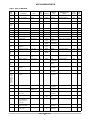
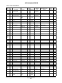
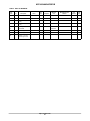
1
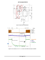
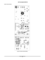
NCP4354AADAPGEVB 65 W Off-Line Adapter Featuring Very Low No-Load Power Consumption Evaluation Board User's Manual http://onsemi.com EVAL BOARD USER’S MANUAL Overview Key Features • • • • • When designing an offline Ac-Dc power adapter, one key consideration is the power consumption in standby mode. Standby power consumption, also sometimes referred to as vampire power or phantom load, is the power consumed by electronic devices when they are switched off, but still plugged into the wall. It is estimated that standby power accounts for nearly 10% of the energy usage in the average American home. One common contributor to vampire power in the home is notebook adapters. These adapters spend a lot of time left underneath desks with the notebook computer disconnected or powered off. The following design note features the latest techniques for minimizing the standby power consumption of a 65 W notebook adapter. When focusing on the no load power consumption of an adapter design, the key losses need to be identified. Switching losses and circuit biasing must be minimized or eliminated completely. The latest technique for minimizing losses during no load is to turn off the Ac-Dc controller and allow the output voltage to drop. Because the adapter is not supplying power, a drop in output voltage is viewed as acceptable. The following design utilizes the NCP1246 flyback controller and the NCP4354A secondary side controller to realize this technique. Both controllers have built-in features focused on minimizing no load input power consumption. Primary side flyback controller NCP1246 is a fixed frequency current mode controller featuring dynamic self supply. It also supports OFF mode and integrated active X2 capacitor discharge feature, which significantly reduces input power at very light load and no load conditions. NCP1246 includes frequency fold-back and skip mode to provide high efficiency in light load. Secondary side controller NCP4354A provides output voltage and current regulation (CCCV operation of whole SMPS), very light load condition detection, OFF mode control and indication LED driver. The NCP4354A is specially design for use in tandem with the NCP1246, detecting no load conditions and triggering OFF mode via the NCP1246 FB pin. © Semiconductor Components Industries, LLC, 2012 September, 2012 − Rev. 0 Constant Voltage Constant Current Regulation (CCCV) Very Low Input Power at Light and No Load High Efficiency Across the Entire Load Range Overpower Protection Universal Mains Operation Circuit Description The primary side uses a flyback topology, providing the advantage of a cost effective power stage design. The power stage operates in both CCM (continuous conduction mode) and DCM (discontinuous conduction mode), allowing it to accept a wide universal input voltage range. The CCM operation provides desired full load performance with good efficiency and low ripple of primary current. The DCM operation then permits an increase of efficiency under the light load conditions, by decreasing the switching losses. The device switches at 65 kHz which represents a good trade-off between switching losses and magnetic core size. The adapter primary side consists of several important sections. The first is an input EMI filter to reduce the conducted EMI to the ac line at the input of the adapter. The EMI filter is formed by common-mode inductors L3 and capacitors C1, C2, C3 and C11 with differential mode inductor L2. The varistor R7 is used to protect the adapter against the line overvoltage peaks. When the power supply is disconnected from the AC mains, X capacitors C2, C13 and Y capacitors C3 and C4 are discharged through HV pin via the following path: rectifying diodes D101, D103, surge protection T network R100, R101 and C100. This feature replaces commonly used discharging resistors and saves approximately 25 mW of input power consumption at 230 Vac. The next block is the rectifier with bulk capacitor. The main power stage of the flyback converter utilizes the low RDSon MOSFET SPP11N60C3 along with a custom designed transformer TR1 KA5038-BL from Coilcraft. The detailed design procedure of a flyback adapter can be found in the application note AND8461/D at ON Semiconductor website: http://www.onsemi.com. 1 Publication Order Number: EVBUM2138/D NCP4354AADAPGEVB is coupled to the NCP1246 primary side controller via the optocoupler. The NCP4354 secondary controller also detects very light load condition via D105, R114, C106, R115 and R116 by OFFDET pin. When light load condition is detected, the primary controller is switched into OFF mode by ON/OFF current sink to DRIVE pin via optocoupler. The built in LED driver indicates primary side operation (when SMPS is not in OFF mode). The LED driver switches with 1 kHz frequency and 12% duty cycle in order to optimize LED efficiency. Secondary rectification is done by a low forward voltage drop Schottky diode NTST30100SG from ON Semiconductor. A simple RC snubber across the secondary rectifier damps the high frequency ringing caused by the unclamped leakage inductance of the secondary side of the transformer and the rectification diode capacitance. Secondary controller NCP4354A provides the output voltage and output current regulation. Output voltage is set by voltage divider R112, R117, R118 and R127, output current is sensed at sense resistor R111. Regulation output Table 1. Parameter Symbol Value Units VIN 85 – 265 VAC Input Frequency fIN 30 – 80 Hz Output Voltage VOUT 19 V Nominal Output Current IOUTNOM 3.4 A Output Current Limit IOUTLIM 3.9 A Efficiency IOUT> 3% IOUTMAX h > 84 % Efficiency IOUT > 25% IOUTMAX h > 90 % Input Voltage NoLoad Power Consumption VIN = 115 V/ 60 Hz PIN 11 mW NoLoad Power Consumption VIN = 230 V/ 50 Hz PIN 21 mW VOUT_PK-PK 50 mV LOADREG 31.7 mV/A Maximal Load Resistance to Stay in OnMode ROUTON 4.4 kW Minimal Load Resistance to Activate OffMode ROUTOFF 5.5 kW 156 x 51 x 27 mm Output Voltage Ripple IOUT = 3.5 A Load Regulation IOUT = 50 mA – 3.5 A Board Dimension http://onsemi.com 2 NCP4354AADAPGEVB Evaluation Board Schematic Figure 1. Evaluation Board Schematic http://onsemi.com 3 NCP4354AADAPGEVB No Load Input Power Consumption Load Regulation Input power consumption was measured by Yokogawa WT210 power meter. Input power was integrated for 20 minutes and averaged from 4 measurements. The main impact on load regulation is the serial resistance of the output common mode inductor and the voltage drop on the output current sensing resistor (65.5 mV @ 3.9 A). Output voltage is sensed in front of them by resistor divider. Table 2. Input Voltage [V; Hz] Input Power [mW] 85 V; 60 Hz 9 115 V; 60 Hz 11 230 V; 50 Hz 21 265 V; 50 Hz 25 19,100 VO UT [V] 19,050 115V 60Hz 19,000 230V 50Hz 18,950 18,900 18,850 0,00 0,50 1,00 1,50 2,00 2,50 3,00 3,50 IO UT [A] Figure 2. Load Regulation is 31.7 mV/A Load Characteristic voltage starts to be limited to keep current at a level given by sensing resistor R111 and voltage threshold of 62.5 mV at current OTA sensing pin ISNS. The following load characteristic shows how current limitation works. When output current reaches 3.9 A, output http://onsemi.com 4 NCP4354AADAPGEVB Figure 3. Load Regulation is 31.7 mV/A Efficiency 95 Efficiency [%] 90 85 80 75 VIN = 230 Vac VIN = 115 Vac 70 0,0 0,5 1,0 1,5 2,0 2,5 IOUT [A] Figure 4. Converter Efficiency for Low and High Line http://onsemi.com 5 3,0 3,5 NCP4354AADAPGEVB Output Voltage Ripple 2 − VOUT (AC) 4 − IOUT Figure 5. VIN = 230 VAC, IOUT = 100 mA, Primary Controller is in Skip Mode, DVOUTPK−PK = 90 mV 2 − VOUT (AC) 4 − IOUT Figure 6. VIN = 230 VAC, IOUT = 500 mA, DVOUTPK−PK = 90 mV http://onsemi.com 6 NCP4354AADAPGEVB 2 − VOUT (AC) 4 − IOUT Figure 7. VIN = 230 VAC, IOUT = 1.0 A, DVOUTPK−PK = 50 mV 2 − VOUT (AC) 4 − IOUT Figure 8. VIN = 230 VAC, IOUT = 3.5 A, DVOUTPK−PK = 50 mV http://onsemi.com 7 NCP4354AADAPGEVB OFF Mode primary FB voltage below the off mode detection level (Figure 11 B). When the primary side detects off mode, FB pull up current is decreased to save energy. After that the FB pull down current through optocoupler can be lower. The secondary side stops sinking additional current by voltage OTA after VSNS voltage drops below VREF to save output capacitor energy (Figure 12 C). Off mode is interrupted when VOUT falls below the VMIN threshold that is detected by VMIN comparator (Figure 9 D). ONOFF current then disappears and primary side FB voltage increases. When primary FB voltage is within operation range, the primary controller starts to operate. The output capacitor is then recharged to nominal output voltage. Off-mode is activated, when output current is below set level. In this design, the off-mode threshold is set to approximately 3.5 mA. This condition is detected by OFFDET comparator through additional rectifier (D105) with bulk capacitor (C106) and voltage divider (R115 and R116). C106 charging current is limited by R114 to avoid full recharge of C106 by short and sporadic pulses in deep skip mode. When very light load is detected, ONOFF current starts to be sunk by the DRIVE pin. The internal pull up current source is connected to VSNS pin and increases its voltage (Figure 10 A). Thanks to this current, voltage OTA starts to sink limited current to help ONOFF current pull the Low VOUT is detected, output capacitor is recharged D 1 − Primary DRV 2 − VOUT (AC) 3 − DRIVE pin 4 − IOUT Figure 9. VIN = 230 VAC, IOUT = 0 A, Off−mode Period tOFFMODE = 77.5 s, VOUTMIN = 2.8 V http://onsemi.com 8 NCP4354AADAPGEVB A 1 − Primary DRV 2 − VOUT 3 − VSNS pin 4 − OFFDET pin Off mode is activated − IBIASV starts to flow Figure 10. VIN = 230 VAC, IOUT = 0 A, Output Capacitor Recharge when VOUT drops below VMIN Level in Off−mode Voltage OTA sinks current A Very light load is detected, converter goes in off mode B C 1 − Primary DRV 2 − VOUT 3 − DRIVE pin 4 − OFFDET pin Figure 11. VIN = 230 VAC, IOUT = 0 A, ON−mode to OFF−mode Transition. The voltage drop on the DRIVE pin indicates the higher voltage OTA sink current (1.5 mA) at time 200 ms after OFF-mode trigger. During this time, the VSNS pin is connected to a 10 mA pull up current source, which increases the voltage at VSNS pin. The OTA stops sinking current 1700 ms after trigger, because VSNS voltage drops below VREF. There is only ONOFF current sunk through OPTO after VSNS < VREF. http://onsemi.com 9 NCP4354AADAPGEVB IBIASV is connected to VSNS C VSNS < VREF, OTA stops sink 1 − Primary DRV 2 − VOUT 3 − DRIVE pin 4 − VSNS pin Figure 12. VIN = 230 VAC, IOUT = 0 A, Same Condition as is shown in Figure 11, but VOFFDET is replaced by VSNS. This waveform shows the time when internal current source (IBIASV) is connected to VSNS. This allows voltage OTA to sink less current until VSNS voltage is higher than VREF. Load is disconnected Load is connected 1 − Primary DRV 2 − VOUT 3 − DRIVE pin 4 − OFFDET pin Figure 13. VIN = 230 VAC, IOUT = 0 A, 20 W Load Resistor is connected to the Output in Off Mode VOUT quickly drops below VMIN voltage and primary side starts to operate again. The DRIVE waveform shows the point when voltage OTA stops sinking current, because VSNS voltage drops below VREF level. http://onsemi.com 10 NCP4354AADAPGEVB Low VOUT is detected D 1 − Primary DRV 2 − VOUT 3 − DRIVE pin 4 − OFFDET pin ONOFF current disappears Figure 14. VIN = 230 VAC, IOUT = 0 A, zoomed Situation from Figure 13. Cursors show time (3.13 ms) that is necessary to switch primary side from OFF mode to normal operation. The DRIVE waveform shows a small voltage change when VOUT is lower than VMIN and ONOFF current is switched off. Load Detection Speed Up Circuit output capacitors C8, C9, C10 are discharged slower than VCC capacitors C6 and C109, so at VCC the voltage is VOUT-VD109 and transistor Q100 is not conducting. Once a load is connected to the SMPS output in OFF mode, the output capacitors start to be discharged faster by the load than the VCC capacitors are discharged by ICC. The voltage difference between output capacitors and VCC capacitors forces Q100 to conduct current through R124 into the OFFDET divider. OFFDET voltage is increased by additional current and when it crosses 10% of VCC threshold, off mode is ended. When a load is connected to the SMPS in off mode, the output capacitors have to be discharged below VMIN level in order to re-start the primary side. The output capacitor discharging may take too long for some applications. Figure 15 shows an external speed up circuit (load detection circuit) that consists of D112, R124, R125, Q100, C6 and removed R123. This circuit uses the NCP4354A OFFDET pin. When the OFFDET voltage goes above 10% of VCC threshold, off mode is ended. Raising the OFFDET voltage can be used to end OFF mode sooner than waiting for VOUT to drop below VMIN level. When there is no load in off mode, http://onsemi.com 11 NCP4354AADAPGEVB Figure 15. Speed up Circuit Schematic Load is connected in off mode Off mode starts Off mode ends 1 − Primary DRV 2 − VOUT 3 − VCC pin 4 − OFFDET pin Figure 16. VIN = 230 VAC, IOUT = 0 A 1 A, Load is connected to the Output of Off Mode http://onsemi.com 12 NCP4354AADAPGEVB Load is connected in off mode Off mode starts Off mode ends 1 − Primary DRV 2 − VOUT 3 − VCC pin 4 − OFFDET pin Figure 17. Zoomed Situation from Figure 16. Cursors show time (4 ms) that elapsed from load connection to primary side turn-on. Load is connected in off mode Off mode starts 1 − Primary DRV 2 − VOUT 3 − VCC pin 4 − OFFDET pin Off mode ends Figure 18. VIN = 230 VAC, RLOAD = 2 kW W 2 kW, Load is connected to the Output in Off Mode http://onsemi.com 13 NCP4354AADAPGEVB 1 − Primary DRV 2 − VOUT 3 − VCC pin 4 − OFFDET pin Load is connected in off mode Figure 19. Zoomed Situation from Figure 18. Cursors show time (392 ms) that elapsed from load connection to primary side turn-on. Active X2 Capacitor Discharge Mains is disconnected X2 cap discharging 32 ms AC detect timer 1 − Input line 1 2 − Input line 2 3 − Primary VHV pin 4 − Primary DRV pin Figure 20. VIN = 230 VAC, IOUT = 1.0 A, when the AC mains is disconnected, 32 ms detection timer is started. After this time, the X2 cap is discharged. Discharging time is much shorter than required by safety standards (37 ms << 1 s) http://onsemi.com 14 NCP4354AADAPGEVB Transient Response Output Current Transients Current slew rate is 125 mA / 1 ms for all transients. 2 − VOUT (AC) 4 − IOUT Figure 21. VIN = 115 VAC, IOUT = 1.0 − 3.5 A, VOUT_DROP = 256 mV 2 − VOUT (AC) 4 − IOUT Figure 22. VIN = 115 VAC, IOUT = 3.5 − 1.0 A, VOUT_OVERSHOOT = 242 mV http://onsemi.com 15 NCP4354AADAPGEVB 2 − VOUT (AC) 4 − IOUT Figure 23. VIN = 230 VAC, IOUT = 1.0 − 3.5 A, VOUT_DROP = 254 mV 2 − VOUT (AC) 4 − IOUT Figure 24. VIN = 230 VAC, IOUT = 3.5 − 1.0 A, VOUT_OVERSHOOT = 242 mV http://onsemi.com 16 NCP4354AADAPGEVB Output Voltage Transients Electronic load is not fast enough to start sinking and keep output Output capacitor discharging − can‘t be controlled by NCP4354A voltage at set point when there is voltage transient 1 − Primary DRV pin 2 − VOUT 4 − IOUT Figure 25. VIN = 230 VAC, VOUT = 12 − 17 V 1 − Primary DRV pin 2 − VOUT 4 − IOUT Figure 26. VIN = 230 VAC, VOUT = 5 − 17 V http://onsemi.com 17 NCP4354AADAPGEVB Output Voltage to Current Transient 1 − Primary DRV pin 2 − VOUT 4 − IOUT Output capacitor discharging − can‘t be controlled by NCP4354A Figure 27. VIN = 230 VAC, VOUT = 12 V to ROUT = 200 W 1 − Primary DRV pin 2 − VOUT 4 − IOUT Figure 28. VIN = 230 VAC, VOUT = 5 V to ROUT = 40 W http://onsemi.com 18 NCP4354AADAPGEVB Open Loop Transfer Characteristics Voltage Control Loop Transfer Characteristic Phase margin is never lower than 50° Gain margin is never lower than 13 dB Crossover frequency is between 0.6 − 0.75 kHz 40 150 20 100 10 50 0 0 TR2/° TR1/dB 30 -10 -50 -20 -100 -30 -40 -150 102 103 104 105 f/Hz TR1: Mag(Gain) TR2: Phase(Gain) Figure 29. VIN = 85 VAC, IOUT = 100 mA 40 150 20 100 10 50 0 0 TR2/° TR1/dB 30 -10 -50 -20 -100 -30 -40 -150 102 103 104 f/Hz TR1: Mag(Gain) TR2: Phase(Gain) Figure 30. VIN = 85 VAC, IOUT = 1.0 A http://onsemi.com 19 105 NCP4354AADAPGEVB 40 150 20 100 10 50 0 0 TR2/° TR1/dB 30 -10 -50 -20 -100 -30 -40 -150 102 103 104 105 f/Hz TR1: Mag(Gain) TR2: Phase(Gain) Figure 31. VIN = 85 VAC, IOUT = 3.5 A 40 150 20 100 10 50 0 0 TR2/° TR1/dB 30 -10 -50 -20 -100 -30 -40 -150 102 103 104 105 f/Hz TR1: Mag(Gain) TR2: Phase(Gain) Figure 32. VIN = 265 VAC, IOUT = 100 mA 40 150 20 100 10 50 0 0 TR2/° TR1/dB 30 -10 -50 -20 -100 -30 -40 -150 102 103 104 f/Hz TR1: Mag(Gain) TR2: Phase(Gain) Figure 33. VIN = 265 VAC, IOUT = 2.0 A http://onsemi.com 20 105 NCP4354AADAPGEVB 40 150 20 100 10 50 0 0 TR2/° TR1/dB 30 -10 -50 -20 -100 -30 -40 -150 102 103 104 105 f/Hz TR1: Mag(Gain) TR2: Phase(Gain) Figure 34. VIN = 265 VAC, IOUT = 3.5 A Current Control Loop Transfer Characteristic Phase margin is never lower than 35° Gain margin is never lower than 18 dB Crossover frequency is between 100 − 200 Hz 40 150 20 100 10 50 0 0 TR2/° TR1/dB 30 -10 -50 -20 -100 -30 -40 -150 101 102 103 104 f/Hz TR1: Mag(Gain) TR2: Phase(Gain) Figure 35. VIN = 230 VAC, IOUT = 3.9 A, VOUT = 15 V http://onsemi.com 21 105 NCP4354AADAPGEVB 40 150 20 100 10 50 0 0 TR2/° TR1/dB 30 -10 -50 -20 -100 -30 -40 -150 101 102 103 104 105 f/Hz TR1: Mag(Gain) TR2: Phase(Gain) Figure 36. VIN = 115 VAC, IOUT = 3.9 A, VOUT = 15 V 40 150 20 100 10 50 0 0 TR2/° TR1/dB 30 -10 -50 -20 -100 -30 -40 -150 101 102 103 104 105 f/Hz TR1: Mag(Gain) TR2: Phase(Gain) Figure 37. VIN = 230 VAC, IOUT = 3.9 A, VOUT = 10 V 40 150 20 100 10 50 0 0 TR2/° TR1/dB 30 -10 -50 -20 -100 -30 -40 -150 101 102 103 104 f/Hz TR1: Mag(Gain) TR2: Phase(Gain) Figure 38. VIN = 115 VAC, IOUT = 3.9 A, VOUT = 10 V http://onsemi.com 22 105 NCP4354AADAPGEVB 40 150 20 100 10 50 0 0 TR2/° TR1/dB 30 -10 -50 -20 -100 -30 -40 -150 101 102 103 104 105 f/Hz TR1: Mag(Gain) TR2: Phase(Gain) Figure 39. VIN = 230 VAC, IOUT = 3.9 A, VOUT = 5 V 40 150 20 100 10 50 0 0 TR2/° TR1/dB 30 -10 -50 -20 -100 -30 -40 -150 101 102 103 104 f/Hz TR1: Mag(Gain) TR2: Phase(Gain) Figure 40. VIN = 115 VAC, IOUT = 3.9 A, VOUT = 5 V http://onsemi.com 23 105 NCP4354AADAPGEVB Conducted Emission Quasi−peak 70 65 60 Level [dBuV] 55 50 45 40 35 30 25 20 100 1000 Frequency [kHz] 10000 Figure 41. VIN = 115 VAC, IOUT = 3.5 A 80 70 Level [dBuV] 60 50 40 30 20 100 1000 Frequency [kHz] 10000 Figure 42. VIN = 230 VAC, IOUT = 3.5 A Result Summary Special thanks go to companies Coilcraft, Epcos and Würth that provided samples of their components for this evaluation board. The NCP1246 and NCP4354 controllers allow building cost effective, easy to design and high efficiency power supplies with very low no load input power consumption. http://onsemi.com 24 NCP4354AADAPGEVB Top Side Assembly Figure 43. Top Side Assembly http://onsemi.com 25 NCP4354AADAPGEVB Bottom Side Assembly Figure 44. Bottom Side Assembly http://onsemi.com 26 NCP4354AADAPGEVB Table 3. BILL OF MATERIAL Substitution Allowed Lead Free MCCA000722 Yes Yes Kemet C0805C104K5RAC Yes Yes 0805 Kemet C0805C102K5RAC Yes Yes - 0805 - - Yes Yes 33 nF 10% 0805 Kemet C0805C333K5RAC Yes Yes Ceramic Capacitor 180 nF 10% 0805 Kemet C0805C184K5RAC Yes Yes 1 Ceramic Capacitor 3.3 nF 10% 0805 Kemet C0805C332K5RAC Yes Yes 1 Ceramic Capacitor 1.0 mF 0805 Kemet C0805C105K5RAC Yes Yes C111 1 Ceramic Capacitor 1.2 nF 10% 0805 Kemet C0805C122K5RAC Yes Yes C12 1 Bulk Capacitor 100 mF / 400 V 20% Through Hole United Chemi-Con EKXG401ELL101MMN3S Yes Yes C13 1 Ceramic Capacitor 1.2 nF / 630 V 5% Disc Radial TDK Corporation FK26C0G2J122J Yes Yes C2, C11 2 Suppression Film Capacitors 100 nF 10% Through Hole Epcos B32922C3104K Yes Yes C4 1 Electrolytic Capacitor 47 mF / 50 V 20% Radial Koshin KLH-050V470ME110 Yes Yes C1, C3, C5 1 Ceramic Capacitor 2.2 nF / X1 / Y1 20% Disc Radial Murata DE1E3KX222MA5B Yes Yes C6 1 Electrolytic Capacitor NU (47 mF / 50 V) 20% Radial Koshin KLH-050V470ME110 Yes Yes C7 1 Ceramic Capacitor 5.6 nF / 630 V 5% Radial TDK Corporation FK20C0G2J562J Yes Yes C8, C9, C10 3 Electrolytic Capacitor 470 mF / 25 V 20% Radial Panasonic ECG ECA-1EHG471 Yes Yes D1 1 Standard Recovery Rectifier 1N4007 - DO41-10B ON Semiconductor 1N4007G No Yes D100, D110 2 Diode MMSD4148 - SOD123 ON Semiconductor MMSD4148T3G No Yes D101, D102, D103, D104, D105, D106, D107, D108, D111 8 Standard Recovery Rectifier MRA4007 - SMA ON Semiconductor MRA4007T3G No Yes D109 1 Zener diode MMSZ15 5% SOD123 ON Semiconductor MMSZ15T3G No Yes D112 1 Diode NU (MMSD4148) - SOD123 ON Semiconductor MMSD4148T3G Yes Yes D2 1 Diode Schottky 100 V, 30 A NTST30100SG - TO220 ON Semiconductor NTST30100SG Yes Yes F1 1 Fuse (MST ser.) 1.6 A - Through Hole Schurter Inc 0034.6617 Yes Yes IC100 1 Fixed Frequency Current Mode Controller for Flyback Converters NCP1246B65 - SOIC-08 ON Semiconductor NCP1246BD065R2G No Yes IC101 1 Secondary Side Off-Mode Controller NCP4354A SOIC-08 ON Semiconductor NCP4354ADR2G No Yes L1 1 WE-CMB Common Mode Choke 14 mH 744 841 414 Würth Elektronik 744 841 414 Yes Yes Value Tolerance Footprint Manufacturer Ceramic Capacitor 68 pF / 1000 V 5% 1206 Multicomp 2 Ceramic Capacitor 100 nF 10% 0805 C102 1 Ceramic Capacitor 1.0 nF 10% C103, C107, C110 3 Ceramic Capacitor NU C105 1 Ceramic Capacitor C106 1 C108 C109 Designator QTY C100 1 C101, C104 Description - http://onsemi.com 27 Manufacturer Part Number NCP4354AADAPGEVB Table 3. BILL OF MATERIAL Designator QTY Description Value L2 1 WE-FI Leaded Toroidal Line Choke 150 mH L3 1 Power Line Choke 2 x 20 mH L4 1 WE-TI Radial Leaded Wire Wound Inductor 1.0 mH LED1 1 LED 3 mm Green LED-3MM-GR EEN NTC1 1 Sensing NTC Thermistor OK1 1 Q1 Substitution Allowed Lead Free 744 701 8 Yes Yes Epcos B82734W2202B030 Yes Yes Würth Elektronik 744 772 010 Yes Yes Manufacturer Tolerance Footprint 20% 744 701 8 Würth Elektronik Manufacturer Part Number - B82734W 20% Radial - Through Hole Vishay TLHG4400 Yes Yes 330 kW 5% Disc Radial Vishay NTCLE100E3334JB0 Yes Yes Optocoupler PC817 - 4-DIP Sharp PC817X2J000F Yes Yes 1 N MOSFET Transistor SPP11N60C3 - TO220 Infineon SPP11N60C3 Yes Yes Q100 1 Transistor PNP NU (BC807-40) SOT23 ON Semiconductor BC807-40LT1G Yes Yes R1 1 Resistor 2.2 W 1% 0207 Vishay MBB02070C2208FRP00 Yes Yes R100, R108 2 Resistor SMD 2.2 W 1% 0805 Rohm MCR10EZHFL2R20 Yes Yes R101, R102 2 Resistor SMD 2.7 kW 0806 Rohm MCR10EZPF2701 Yes Yes R103 1 Resistor SMD 680 W 1% 0805 Rohm MCR10EZPF6800 Yes Yes R104, R105, R106, R107 4 Resistor SMD 1.0 W 1% 1206 Rohm MCR18EZHFL1R00 Yes Yes R109 1 Resistor SMD 22 W 1% 0805 Rohm MCR10EZPF22R0 Yes Yes R110 1 Resistor SMD 10 kW 1% 0805 Rohm MCR10EZPF1002 Yes Yes R111 1 Resistor SMD 16 mW 1% 1206 Panasonic ERJ-8BWFR016V Yes Yes R112 1 Resistor SMD 18 kW 0805 Rohm MCR10EZPF1802 Yes Yes R113, R119, R121 3 Resistor SMD 1.0 kW 1% 0805 Rohm MCR10EZPF1001 Yes Yes R114 1 Resistor SMD 270 W 1% 0805 Rohm MCR10EZHF2700 Yes Yes R115 1 Resistor SMD 300 kW 0805 Rohm MCR10EZPF3003 Yes Yes R116 1 Resistor SMD 56 kW 0805 Rohm MCR10EZPF5602 Yes Yes R117 1 Resistor SMD 180 kW 0805 Rohm MCR10EZPF1803 Yes Yes R118, R127 2 Resistor SMD 15 kW 0805 Rohm MCR10EZPF1502 Yes Yes R120 1 Resistor SMD 5.6 kW 0805 Rohm MCR10EZPF5601 Yes Yes R122 1 Resistor SMD 3.9 kW 0805 Rohm MCR10EZPF3901 Yes Yes R123 1 Resistor SMD 220 W 0805 Rohm MCR10EZPF2200 Yes Yes R124 1 Resistor SMD NU (220 kW) 0805 Rohm MCR10EZPF2203 Yes Yes R125 1 Resistor SMD NU (100 kW) 0805 Rohm MCR10EZPF1003 Yes Yes R126 1 Resistor SMD 33 kW 0805 Rohm MCR10EZPF3302 Yes Yes R128 1 Resistor SMD 82 kW 0805 Rohm MCR10EZPF8202 Yes Yes R2, R3 2 Resistor 330 kW 1% 0207 Vishay HVR2500003303FR500 Yes Yes R4 1 Resistor Through Hole, High Voltage 4.7 MW 5% Axial Lead Welwyn VRW37-4M7JI Yes Yes R5 1 NTC Thermistor Wire Strap - Disc Radial - - Yes Yes R6 1 Surge protecting varistor B72210P2301 K101 20% Disc Radial Epcos B72210P2301K101 Yes Yes http://onsemi.com 28 NCP4354AADAPGEVB Table 3. BILL OF MATERIAL Designator QTY Description Value Tolerance Footprint 1% 0207 Manufacturer Part Number Substitution Allowed Lead Free Vishay MRS25000C1509FRP00 Yes Yes Manufacturer R7 1 Resistor 15 W TR1 1 Transformer KA5038-BL - KA5038-BL CoilCraft KA5037-BL Yes Yes X1 1 Terminal Block, 2 Way CTB5000/2 - W237-102 Cadem El. CTB5000/2 Yes Yes X2 1 Terminal Block, 3 Way CTB5000/3 - W237-113 Cadem El. CTB5000/3 Yes Yes Q1, D1 2 EMI Suppression Ferrite Bead 742 700 73 - 742 700 73 Würth Elektronik 742 700 73 Yes Yes D2 1 Heat Sink Type 1 - - - - - Yes Yes Q2 1 Heat Sink Type 2 - - - - - Yes Yes Q1, D2 2 TO220 Transistor Insul Pad 1.13 x 0.63” & Bushiings & Screw - - - - TO-220-68 Yes Yes http://onsemi.com 29 NCP4354AADAPGEVB Evaluation Board Photo Figure 45. Evaluation Board Photo ON Semiconductor and are registered trademarks of Semiconductor Components Industries, LLC (SCILLC). SCILLC owns the rights to a number of patents, trademarks, copyrights, trade secrets, and other intellectual property. A listing of SCILLC’s product/patent coverage may be accessed at www.onsemi.com/site/pdf/Patent−Marking.pdf. SCILLC reserves the right to make changes without further notice to any products herein. SCILLC makes no warranty, representation or guarantee regarding the suitability of its products for any particular purpose, nor does SCILLC assume any liability arising out of the application or use of any product or circuit, and specifically disclaims any and all liability, including without limitation special, consequential or incidental damages. “Typical” parameters which may be provided in SCILLC data sheets and/or specifications can and do vary in different applications and actual performance may vary over time. All operating parameters, including “Typicals” must be validated for each customer application by customer’s technical experts. SCILLC does not convey any license under its patent rights nor the rights of others. SCILLC products are not designed, intended, or authorized for use as components in systems intended for surgical implant into the body, or other applications intended to support or sustain life, or for any other application in which the failure of the SCILLC product could create a situation where personal injury or death may occur. Should Buyer purchase or use SCILLC products for any such unintended or unauthorized application, Buyer shall indemnify and hold SCILLC and its officers, employees, subsidiaries, affiliates, and distributors harmless against all claims, costs, damages, and expenses, and reasonable attorney fees arising out of, directly or indirectly, any claim of personal injury or death associated with such unintended or unauthorized use, even if such claim alleges that SCILLC was negligent regarding the design or manufacture of the part. SCILLC is an Equal Opportunity/Affirmative Action Employer. This literature is subject to all applicable copyright laws and is not for resale in any manner. PUBLICATION ORDERING INFORMATION LITERATURE FULFILLMENT: Literature Distribution Center for ON Semiconductor P.O. Box 5163, Denver, Colorado 80217 USA Phone: 303−675−2175 or 800−344−3860 Toll Free USA/Canada Fax: 303−675−2176 or 800−344−3867 Toll Free USA/Canada Email: [email protected] N. American Technical Support: 800−282−9855 Toll Free USA/Canada Europe, Middle East and Africa Technical Support: Phone: 421 33 790 2910 Japan Customer Focus Center Phone: 81−3−5817−1050 http://onsemi.com 30 ON Semiconductor Website: www.onsemi.com Order Literature: http://www.onsemi.com/orderlit For additional information, please contact your local Sales Representative EVBUM2138/D