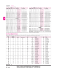
1
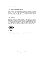
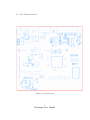
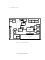
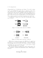
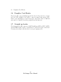
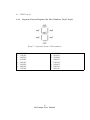
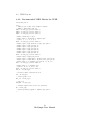
McGumps
McGill University
Microprocessor Systems Board
User Manual
Contents
1 General Information
1.1 User Manual Notation . . . . . . . . . . . . . . . . . . . . . .
1.1.1 Board, Components and Pins . . . . . . . . . . . . . .
1.1.2 Jumpers . . . . . . . . . . . . . . . . . . . . . . . . . .
2 McGumps Configuration and Hardware Reference
2.1 Powering up McGumps . . . . . . . . . . . . . . . . .
2.1.1 Parasitic Power from Parallel Port . . . . . .
2.1.2 External Wall mount supply . . . . . . . . . .
2.1.3 2-Input connector terminal block . . . . . . .
2.2 Programming MSP430 and MAX7128AE . . . . . . .
2.3 RS232C Interface . . . . . . . . . . . . . . . . . . . .
2.4 Oscillators . . . . . . . . . . . . . . . . . . . . . . . .
2.5 Bootstrap Loader . . . . . . . . . . . . . . . . . . . .
2.6 Daughter Card Header . . . . . . . . . . . . . . . . .
2.7 Straight up header . . . . . . . . . . . . . . . . . . .
.
.
.
.
.
.
.
.
.
.
.
.
.
.
.
.
.
.
.
.
.
.
.
.
.
.
.
.
.
.
.
.
.
.
.
.
.
.
.
.
3
3
4
4
7
. 7
. 7
. 7
. 7
. 8
. 9
. 9
. 9
. 11
. 11
3 Programming with MSP430 MCU
12
3.1 Startup . . . . . . . . . . . . . . . . . . . . . . . . . . . . . . 12
3.2 Resetting and Aborting Programs . . . . . . . . . . . . . . . . 12
3.3 Flashing LED example . . . . . . . . . . . . . . . . . . . . . . 12
4 Programming with MAX7128AE CPLD
14
4.1 Notes on Programming Max7128AE . . . . . . . . . . . . . . . 14
4.2 CPLD Layout . . . . . . . . . . . . . . . . . . . . . . . . . . . 15
4.2.1 Segment Pattern Required for Hex Numbers (SegG..SegA) 18
4.2.2 Recommended VHDL Header for CPLD . . . . . . . . 19
List of Figures
1
2
3
4
5
6
7
Board Layout . . . . . . . . . . . . . . . .
Logical Block Diagram . . . . . . . . . . .
DC Power Connector . . . . . . . . . . . .
Power Supply DC Jack . . . . . . . . . . .
Bootstrap circuit connection to MSP430 .
Bootstrap circuit connection to serial port
Segment Pattern for Hex numbers . . . . .
.
.
.
.
.
.
.
.
.
.
.
.
.
.
.
.
.
.
.
.
.
.
.
.
.
.
.
.
.
.
.
.
.
.
.
.
.
.
.
.
.
.
.
.
.
.
.
.
.
.
.
.
.
.
.
.
.
.
.
.
.
.
.
.
.
.
.
.
.
.
. 5
. 6
. 7
. 8
. 10
. 10
. 18
1: General Information
1
General Information
The board consists of a 6.5 inch by 6 inch 2-layer printed circuit board layer
(PCB) that provides the platform for interface and power connections to
both the MSP430 MCU chip and the MAX7128AE PLD.
Figure 1 shows the McGumps board layout and locations of the major
components as viewed from the component side of the board.
Figure 2 shows a system block diagram depicting the logical relationship
and interconnections within McGumps and with external equipment.
Hardware features of McGumps include:
• Power supply +5V DC jack and connector terminal input
• RSR232 interface (U3)
• Smart Card Media socket (U11)
• Hex Display (U9)
• iButton clip (U15)
• 8MHz crystal (X1) and 32.768KHz crystal (X2)
• 40MHz oscillator (U10)
• MSP430F149 MCU (U1)
• MAX7128AE PLD (U8)
• Serial communication interface (J10)
• Parallel port interface (J20)
• Headers
– 2X10 headers (H1) for connection to PLD and HEX display
– Shrouded straight 40-pin header (H2) for connection to the daughter card
1.1
User Manual Notation
The following convention is used to identify boards, jumper, other components and pins.
3
McGumps User Manual
1.1 User Manual Notation
1.1.1
Board, Components and Pins
Each board has a serial number on the bottom (viewed from the component
side) left of the board. Components, oscillators, headers, resistors and capacitors are labeled “U”, “H”, “R”, “C”, “X” respectively. Each alphabet
is followed by a number indicating the unique component. For example, U8
refers to the MAX7128AE CPLD.
1.1.2
Jumpers
Jumpers are labeled “J”, followed by a number. The figure below indicates
when a jumper block is place on pin2 and pin3 of a 3-pin jumper JXX. The
solid line around the pins depicts the jumper placement. For an open connection (no jumper blocks required), the pins of the jumper are not surrounded
by any line. The open connection is illustrated by the notation for JYY.
Note that pin 1 on the jumpers is explicitly labeled and has a square
connector on the board.
4
McGumps User Manual
1.1 User Manual Notation
Figure 1: Board Layout
5
McGumps User Manual
1.1 User Manual Notation
Figure 2: Logical Block Diagram
6
McGumps User Manual
2: McGumps Configuration and Hardware Reference
2
2.1
McGumps Configuration and Hardware Reference
Powering up McGumps
McGumps can be operated from a variety of power supplies. The power
supply (except when powering from parallel port) is regulated through a
3.3V regulator and a reset-able 500mA fuse.
2.1.1
Parasitic Power from Parallel Port
The MSP430F149 MCU can operate from a regulated 1.8V to 3.6V supply.
For low power applications, the parallel port supplies 2.8V to the board. This
will not be enough to power for using the MAX7128AE PLD. When using
power from the parallel port, remember to remove the CPLD power supply
from the board. The RS-232C serial interface should also be unplugged as it
reduces power consumption and allows for a higher voltage on the bus.
2.1.2
External Wall mount supply
With the use of the 78M33C regulator, the MCGUMPS can operate from an
external wall supply. The power connector is a 2.5mm barrel connector.
Figure 3: DC Power Connector
2.1.3
2-Input connector terminal block
A minimum Vin = 4.3V is recommended for the 3.3V regulator. This can be
supplied from the standard DC lab power supply. It is recommended that a
5V regulated DC power supply be used if the external screen daughter card
is used, because the backlight requires 5.0V on the unregulated 5V bus. It is
also recommended that the voltage on the input power line should not exceed
10V because of user safety concerns and the protection of some of the 3.3V
digital lines.
7
McGumps User Manual
2.2 Programming MSP430 and MAX7128AE
Figure 4: Power Supply DC Jack
2.2
Programming MSP430 and MAX7128AE
The MSP430 can be programmed through JTAG chain using Altera/Quartus
and also through CrossWorks. By using the jumper settings below, the MCU
and CPLD can be programmed using CrossWorks and Alter/Quartus respectively.
1
J18
1
J21
1
J22
1
J19
8
McGumps User Manual
2.3 RS232C Interface
2.3
RS232C Interface
Component U3 is the MAX3223 RS-232C line driver/receiver for interfacing
with CPU terminal/bootstrap loader and MSP430. The driver on board is
in normal operation with auto-power down enabled. During this mode of
operation, if the device does not sense a valid RS-232C signal, the driver
outputs are disabled. Data is valid if receiver input voltage is greater that
2.7V or less than -2.7V or has been between -0.3V and 0.3V for less than 30s.
For CPU terminal interface and bootstrap loader functionality (if available):
1
J12, J13
1
J5, J6
Refer to the main board schematics for MCU connections pins to the
MAX3223.
2.4
Oscillators
McGumps has the following three oscillators available.
Oscillator
40 MHz Oscillator
8MHz Crystal
32.768 KHz Crystal
2.5
On-board Label
U10
X1
X2
Connections
Pin 83 of MAX7128AE CPLD
Pin 52 and 53 of MPS430 MCU
Pint 8 and 9 of MSP430 MCU
Bootstrap Loader
The MSP430 bootstrap loader (BSL) enables users to communicate with
embedded memory in the MSP430 microcontroller during the prototyping
phase, final production, and in service. Both the programmable memory
(flash memory) and the data memory (RAM) can be modified as required.
The commonly used UART protocol with RS232C interfacing is supported,
9
McGumps User Manual
2.5 Bootstrap Loader
allowing flexible use of both hardware and software. To use the bootstrap
loader, a specific BSL entry sequence has to be applied to specific device
pins. An added sequence of commands initiates the desired function. A boot
loading session can be exited by continuing operation at a defined user program address, or by the reset condition. Access to the MSP430 memory via
the bootstrap loader is protected against misuse by a user-defined password.
The bootstrap circuitry is located in the bottom left corner of the board.
To initiate the bootstrap loader, ensure that following jumper settings
have been made:
1
1
J30,J31
J30,J31
1
J32,J33
Connected
1
J32,J33
Disconnected
Figure 5: Bootstrap circuit connection to MSP430
Figure 6: Bootstrap circuit connection to serial port
While in the bootstrap mode power to the MSP430 can be supplied via
the Serial port. To power up the MSP430 using the bootstrap circuitry make
sure that jumper J29 is in 1-2 position. If you wish to power the board using
an external power source and use that source to power up the bootstrap
circuit change the jumper J29 to 2-3 position.
Once properly connected you must use Bootstrap loading software. For
more information, consult the Texas Instruments website MSP430 Application notes.
10
McGumps User Manual
2.6 Daughter Card Header
2.6
Daughter Card Header
The header H2 connects MSP430 pin P1.X, P2.X, P3.X and P6.X to a daughterboard. The daughter board will be connected using a flat 40-wire cable.
Refer to the schematics for exact header-pin connections. Refer to MSP430
user guide for digital I/O and its peripheral module function.
2.7
Straight up header
The 40 pins header H1 connects to MAX7128AE pin OUTA, OUTC, OUTD,
and the HEX display. Refer to schematics for exact header-pin connections.
You may wire-wrap to this header for your prototyping needs.
11
McGumps User Manual
3: Programming with MSP430 MCU
3
Programming with MSP430 MCU
This section details steps necessary to begin programming with the MCU.
This includes a brief outline on setting up the McGumps for operation and
an example on loading and executing a program on the MCU.
3.1
Startup
1. Configure McGumps if required. See Section 2.2.
2. Power up the board. See Section 2.1 for more on how to power up the
MCGUMPS.
3. Connect the board to the terminal.
4. Apply power to the board.
3.2
Resetting and Aborting Programs
The MCU can be reset by pressing the reset button (SW1). This operation
has the effect of restarting the program currently loaded on the MCU. If
the program running on the MCU has to be aborted, the board has to be
powered down by removing the power connection.
3.3
Flashing LED example
1. Start (Rowley Associates Limited) CrossWorks MSP430 1.2.
2. Create new solution by File → New → New Blank Solution
3. In New Project window, choose TI FET Projects folder under Project
Types: and choose FET430P 140 C Project under templates: then
click OK.
4. A demo the flashes the LED is shown in the main.c tab in the main
frame.
5. To compile, Build→Build Solution. In the Output frame, the build log
indicates that build is complete.
12
McGumps User Manual
3.3 Flashing LED example
6. Ensure that the jumpers are set-up to enable programming of the
MSP430 MCU.
7. Ensure that the parallel port 1 is connected to the board. Then, choose
Target→Connect FET on LPT1 to connect to the MSP430 microprocessor.
8. Choose Debug→Start Debugging to download flashing LED example
on to MSP430 microprocessor. The LED should start flashing.
Comments: In the above example, the energy needed for operation is
taken from the parallel port (parasitic power ).
13
McGumps User Manual
4: Programming with MAX7128AE CPLD
4
Programming with MAX7128AE CPLD
4.1
Notes on Programming Max7128AE
Be sure to use the floorplan editor or a pin configuration file to declare the
pinout of the device before programming it on McGumps. The default state
of any pins that are not driven explicitly by the design in LO (0). A pin
can also be defined using Assign→Pin→Location→Chip from Max+Plus II
menus.
The exact device used should be the EPM7128AELC84-10. The speed
grade is the last 2 digits of the part number and may be subject to variation depending on board lot. Be sure to confirm exact part number before programming the CPLD using the Max+Plus II software. The exact
chip can be selected using Assign→Device→Max7000AE (Device Family)→
EPM7128AELC-XX (choose XX depending on your specific chip).
The chip can only be programmed in ByteBlasterMV mode using a computer’s parallel port (LPT1). This setting can be selected by going to the
Options→Hardware Setup menu in Max+Plus II.
To program the device, once you have the design ready, the device selected, the floorplan complete and the programmer type chosen:
1. Compile the device by selecting Max+Plus II→Compiler→Start from
the program menu to create the .POF and/or .SOF files needed for
programming.
2. Program the device by selecting Max+Plus II→Programmer→Program.
Make sure that the chip is installed and powered before attempting to
program it. Also make sure that no other program has control of the parallel
port before attempting to program. This situation will occur when trying
to program the CPLD after programming the MSP430 through the parallel
port. Any combination of the following may be required for Max+Plus II to
regain control of the parallel port:
1. Release parellel port in Crossworks by selecting Target→Disconnect.
2. Cycle the power on the McGill University Evaluation Board.
3. Disconnect and reconnect the parallel cable from the connector
14
McGumps User Manual
4.2 CPLD Layout
4.2
CPLD Layout
The CPLD used is the 84-pin PLCC version of the Altera MAX7128AE. It
contains 128 macrocells in 8 logic array blocks for an effective size of 2500
usable gates. There are a total of 68 I/O pins including those dedicated to
JTAG. All inputs are 5V and 3.3V compatible in the current setting. The
output voltage for all I/O is hardwired to 3.3V, but other voltages are possible
using this particular device. The ports connected to the microprocessor are
labeled with numbers (Ports 1, 2, 4 and 5) corresponding to the I/O pins
on the microprocessor. The Ports independent of the microprocessor are
labeled with letters (Ports A, B, C and D). The output ports of the chip can
be designed with up to 6 separate output enables.
The clock can be selected from one of two inputs GCLK1 and GCLK2.
GCLK1 (pin 83) is tied to the output of the 40.000 MHz oscillator. The
oscillator is equipped with an ultra-low power standby mode than can be
enabled by driving pin 73 (Port A [7]) high. A high or open is required for
the oscillator to operate; a low at pin 73 will disable the oscillator. The
alternate clock is GCLK2 (pin 2) and is hardwired to the SPI CLK input
from the microcontroller (Input Port 5 [7]).
Pin 84 (OE) can be used as an externally input active high output enable
for the device. Each register clear function can be individually driven by the
active-low dedicated global clear pin, GCLRn (pin 1). Upon power-up, each
register in a MAX 7000AE device may be set to either a high or low state.
This power-up state is specified at design entry.
The JTAG interface is connected to the device using pins 14 (TDI), 23
(TMS), 62 (TCK) and 71 (TDO). Hence, these pins are unavailable to the
user.
15
McGumps User Manual
4.2 CPLD Layout
LAB
A
A
A
A
A
A
A
A
C
C
C
C
C
C
C
C
84-Pin
PLCC
Pin Number
12
11
10
9
8
6
5
4
31
30
29
28
27
25
24
23
Pin Name
LAB
Port 1[7]
Port 1[6]
Port 1[5]
Port 1[4]
Port 1[3]
Port 1[2]
Port 1[1]
Port 1[0]
Port 5[6]
Port 5[5]
Port 5[4]
Port 5[3]
Port 5[2]
Port 5[1]
Port 5[0]
TMS
D
D
D
D
D
D
D
D
E
E
E
E
E
E
E
E
84-Pin
PLCC
Pin Number
41
40
39
37
36
35
34
33
44
45
46
48
49
50
51
52
16
McGumps User Manual
Pin Name
Port
Port
Port
Port
Port
Port
Port
Port
Port
Port
Port
Port
Port
Port
Port
Port
4[7]
4[6]
4[5]
4[4]
4[3]
4[2]
4[1]
4[0]
2[7]
2[6]
2[5]
2[4]
2[3]
2[2]
2[1]
2[0]
4.2 CPLD Layout
LAB
84-Pin
PLCC
Pin Number
Pin Name
B
B
B
B
B
B
B
B
F
F
F
F
F
F
F
F
G
G
G
G
G
G
G
G
H
H
H
H
H
H
H
H
22
21
20
8
17
16
15
14
54
55
56
57
58
60
61
62
63
64
65
67
68
69
70
71
73
74
75
76
77
79
80
81
Out
Out
Out
Out
Out
Out
Out
D[6]
D[5]
D[4]
D[3]
D[2]
D[1]
D[0]
40-Pin
Connector
Pin Numer
(if applicable)
24
26
28
30
32
34
36
Out
Out
Out
Out
Out
Out
Out
C[0]
C[1]
C[2]
C[3]
C[4]
C[5]
C[6]
12
14
16
18
35
31
33
Out
Out
Out
Out
Out
Out
Out
B[6]
B[5]
B[4]
B[3]
B[2]
B[1]
B[0]
29
27
25
23
21
19
17
Out
Out
Out
Out
Out
Out
Out
Out
A[7]
A[6]
A[5]
A[4]
A[3]
A[2]
A[1]
A[0]
3
5
7
9
10
8
6
4
Notes[1]
Reserved for TDI
Connected to segDP (decimal point) [2]
Connected to CA 1 (common anode digit 1)
Connected to CA 2 (common anode digit 2)
Reserved for TCK
Connected to SegG of hex display [2]
Connected to SegF of hex display [2]
Connected to SegE of hex display [2]
Connected to SegD of hex display [2]
Connected to SegC of hex display [2]
Connected to SegB of hex display [2]
Connected to SegA of hex display [2]
Reserved for TDO
Reserved for Oscillator Standby enable
[1] 40-pin connector also has the following pin assignments:
GND: 11, 15, 22, 37 and 38
5V VDD: 1 and 40
3.3V VDD: 2 and 39
[2] There are two digits on the hex display. The common anode must be tied
high for a digit to be enabled. Each segment must be tied low for it to light
up. Information should switch between the digits at speeds of less than 1
MHz (it was tested at 300 kHz). Hexadecimal Display is labeled as follows.
17
McGumps User Manual
4.2 CPLD Layout
4.2.1
Segment Pattern Required for Hex Numbers (SegG..SegA)
Figure 7: Segment Pattern for Hex numbers
0:
1:
2:
3:
4:
5:
6:
7:
”1000000”
”1111001”
”0100100”
”0110000”
”0011001”
”0010010”
”0000010”
”1111000”
8: ”0000000”
9: ”0011000”
A: ”0001000”
b: ”0000011”
C: ”1000110”
d: “0100001”
E: ”0000110”
F: ”0001110”
18
McGumps User Manual
4.2 CPLD Layout
4.2.2
Recommended VHDL Header for CPLD
entity CPLD_test is
Port (
-- PORT(1,2,4,5) to MSP, can be changed to outputs
-- PORT5(7) should map to SPI_clk
PORT1 : in std_logic_vector(7 downto 0);
PORT2 : in std_logic_vector(7 downto 0);
PORT4 : in std_logic_vector(7 downto 0);
PORT5 : in std_logic_vector(6 downto 0);
--OUTA(7) should map to clk_en
--OUTA(7 downto 0) should map to expansion port
--(pins 3, 5, 7, 9, 10, 8, 6, 4)
OUTA : out std_logic_vector(6 downto 0);
--OUTB(0) maps to segA (drive LO to light; port pin 17)
--OUTB(1) maps to segB (port pin 19)
--OUTB(2) maps to segC (port pin 21)
--OUTB(3) maps to segD (port pin 23)
--OUTB(4) maps to segE (port pin 25)
--OUTB(5) maps to segF (port pin 27)
--OUTB(6) maps to segG (port pin 29)
OUTB : out std_logic_vector(6 downto 0);
--OUTC(4) maps to segDP (port pin 35)
--OUTC(5) maps to Common Anode 1 (HI when in use; port pin 31)
--OUTC(6) maps to Common Anode 2 (HI when in use; port pin 33)
--OUTC(3 downto 0) to expansion port (pins 18, 16, 14, 12)
OUTC : out std_logic_vector(6 downto 0);
--OUTD(6 downto 0) to expansion port
--(pins 36, 34, 32, 30, 28, 26, 24)
OUTD : out std_logic_vector(6 downto 0);
CLK_en : out std_logic;
--oscillator enable, used with aux clock
CLK : in std_logic;
-- used as global clock
SPI_clk : in std_logic;
-- aux clock
GLB_RSTn : in std_logic;
-- internal register reset (active low, pulled HI)
OE : in std_logic
-- pulled up normally, bypass to expansion port pin 22
);
19
McGumps User Manual