1
P
~
tA' f
j
',-",
DESIGN & DATA ACQUISITION at
3-D FORCE SENSOR
Said BOUKERMA
Universite de Technologie de
compiegne - FRANCE
February - June 1989
WPA-rapport nr.0724
ACKNOWLEDGEMENTS
I want to express my gratitude to my coach'Mr P.C. MULDERS for
his kindness and efficient advice.
The organization of my project by the international relations
staff was satisfying.
The nice atmosphere created in the laboratory was very pleasant
thanks to all the students.
I also want to thank the students of I.R.C.E (International
Reception committee of Eindhoven) who involved themselves in the
good march of my stay.
said
BOUKERMA
CONTENTS
Page
I INTR.ODUCTION . . . . . . . . . . . . . . . . . . . . . . . . . . . . . . . . . . . . . . . . 1
I.1 The Engineering Education in the Netherlands ••
I.2 Eindhoven University of Technology ••••••••••.•
I.2.1 The Mechanical Department •••••.•••••••••••.
I.3 My Practical Work ...•••••..•••••••.•••..••••.•
1
1
2
3
II DIFFERENT TEACHING METHODS ••••••..•••..••••••..• 4
II.l Method used ................................... 4
II.2 Other Teaching Methods ••••.••••....•.•...••••• 4
III THE R-T ROOOT ...................................... 6
III.1 The Mechanical Part •.••••••.•••••••••••••••• 6
-III.2 The Actuators •••••••...•.••.•••...•••••••..• 6
III.3 The Interfaces ....................................... 8
III.3.1 The Force Sensor Interface .••••••••••••.•
III.3.1.1 General Information .••...••••••.•.••••
III.3.1.1.a Justification of this Interface •..•
III.3.1.1.b Review of the Previous Interface •..
8
8
8
8
III.3.1.1.c New Ideas . . . . . . . . . . . . . . . . . . . . . . . . . . 9
III.3.1.1.d Other Solutions ....•..••.•••••..••• 11
III.3.1.2 Technical Information •.••..••••••.•••• 11
III.3.1.2.a The SDM 856 •••••••••••.•••••••••.•• 11
III.3.1.2.b The Filter •••••..••••.••••••...•••• 12
III.3.1.2.c Programmable Amplifier: AD 526 •.••. 13
III.3.1.2.d Offset Adjustment •.•..•••••••••.•.• 14
III.3.1.2.e Overrange Detection ••••••.••••••..• 14
III.3.1.2.f Channel Selection •.•••••.•••••••••• 15
III.3.1.2.g Interface Timing .•••.•••..••...•••. 15
III.3.1.2.h Acquisition Speed ••••••..•••••.••.. 15
III.4 The Interface iSBC/Motor Power Amplifier ••.• 16
III.5 The position Interface .••••.••••••.....••.•. 16
III.6 The Interfaced Devices ••••••.•••••••.•.•.... 17
III.6.1 The Force sensor .•.•••••••••••.•••••••••• 18
III.6.1.1 Mechanical Consideration ••••...•...••• 18
III.6.1.2 The Strain Gages ••..••••...•••...•..••. 20
III.6.1.3 Electronic Description •••.•••.••..••.. 21
III.6.2 The Hall Switches ••••••••••••..•..••.•••• 21
III.6.3 The Position Force Sensor ••••••.•.••••••• 21
III.6.4 The Power Servo Amplifier ••••••...•.•..•• 22
........ .... . . . . . . ..... 23
23
IV.l The Communication •••••.••••
24
IV.2 Multibus system
. .... . . . ........
25
IV .,2.1 the Multibus Arbitration •••••
IV THE MULTIPROCESSOR SYSTEM
IV.3 The RAM Memory Board: iSBC 028A
IV.4 Single Board Computers
IV.4.1 iSBC 186/03
IV.4.2 iSBC 86/12
IV.5 Memory Addressing Scheme
V THE SOFTWARE
. . . . . . . . . . . . . . . . . . . . . . .. . . . . . . . . . . . . .
V.l Program Development
V.2 Program structure •••••
V.3 Calculations ••••..
V.4 Interrupt Procedures
V.5 Definition of the Various Modes
V.5.l Test Mode
V.5.2 Replay Mode
V.5.3 Teach Mode
V.6 Peripherals
V.6.l PPI
V.6.2 PIT
V.6.3 PIC .•••..
V.7 Development System
V.7.l Presentation
V.7.2 Compiling and Linking Operations
. . .. .
VI CONCLUSION
VII APPENDICES
. . . .. . . . . . . . . . . . . . . . . . . . . . . . . . . . . . . . . .
26
26
26
27
29
30
30
30
32
33
34
34
34
34
34
34
35
36
37
37
38
39
40
I
1.1
INTRODUCTION
The Engineering Education in the Netherlands
Engineering education at University level in the Netherlands is
not surprising, because the engineering education is not based
like in France on two structures; schools and universities.
In the Netherlands, there are three universities which like the
TUE (Technische Universiteit Eindhoven) award the engineering
degree. The TUE was founded in 1956, the oldest located in Delft
in 1842 and the most recent one located in Twente in 1961.
Technical Universities have a total population of 20,000
students.
The first degree which concludes a course of studies is the
master degree. In engineering subjects, the master degree
entitles the graduate to use the legally protected abbreviation
'Ir' (Engineer) before his name. To get the Doctor degree 'Dr' no
specific courses are required. The student has to be 'Ir' and is
required to carry out original research.
1.2
Eindhoven University of Technology
This university offers nine courses of study which students can
pursue. Engineering titles are granted in the following fields:
• Technology in its social application (60 students)
• Industrial engineering and science management (1150 students)
• Mathematics (360 students)
• Computer Science (438 students)
• Technical physics (529 students)
• Mechanical engineering (872 students)
• Electrical engineering (1083 students)
• Chemical engineering (656 students)
• Architecture, Structural engineering and urban planning
(716 students)
Among these students, 7% are female. The academic and
administrative staff is composed of 2200 persons who have
permitted the delivery of about 9000 diplomas since the opening
of the faculty.
1
I.2.1
The Mechanical Department
This department is the second largest of the university,
subdivided in many sections, Design and Production are the most
significant sections in which the diverse field of mechanics
including scientific research and development and industrial
application are represented.
The courses are focused on eight topics, reflecting the major
sections:
• control and simulation of mechanical manufacturing processes
• Biomedical technology of vital human biological functions
• Design of process equipment for maximum reduction of life
cycle costs
• Non linear dynamics and random vibrations
• High efficiency power transmission and tribology
• Optimization and energy conservation in transport
• Design of machines for making reinforced plastic materials
• Flexible automation and industrial robots
I worked during 5 month in the WPA section (engineering and
automation production) and participated to the FL.A.I.R.project
( FLexible Automation and Industrial Robots ). The research
project flair is financed and directed by the Dutch government.
Its goal is to get some experience in flexible automation and
industrial robotics.
In this project each university has its own task. At the TUE
this program involves both the mechanical and the electrical
department and including relations with private companies.
The programm is divided into five sections:
•
•
•
•
•
The general aspect of automation
The handling of parts
Kinematics and Dynamics of mechanical structures
The drive and control systems and their applications
The arc welding and the sensory system
2
1.3
My Practical Work
Working on the sensory system which is a part of the F.L.A.I.R
project, my coach ir P.C. Mulders is developing a two dimensional
robot. This robot has been built in many steps, with first only
one degree of freedom~ it is now going to get a second one.
The original feature of this robot is the fact that it includes
a force sensor which is used to calculate the forces and moments
applied on the robot.
During my project, I was busy with this force sensor. We had to
establish a link to the computer,which was Analog/digital
interface.
An interface which has been previously built didn't provide
sufficient speed and accuracy.
An interface, of course must be connected to computer.
therefore, I also worked with an INTEL single board iSBC 86/12A
in order to develop the software.
The organization of my work was as follows~ at the beginning I
was to get some information on the robot, the control, the
parallel processing, the Intel boards, the former student's work
and finally to precisely define the field of my work. After that,
my task was to design a new interface eliminated the previous
design efficiencies. This was done in cooperation with my coach
and Mr Henk van Rooy, who helped me a lot in this crucial part of
my project.
Once the design was finished, we didn't have enough time to
build the interface. We let the CTD (technical service of the
university) build it.
At that point, the software had to be written. Before starting
it, we had to choose the language. The assembler which appeared
best adapted to that application seemed too complex to be
mastered, so the pascal was used.
The last part of the work was the coordination of the software
and the hardware, usually the most difficult task.
Unfortunately, the building of the interface required much more
time than expected. So, the interface was not completely tested.
This will be the first step of another project.
3
II
DIFFERENT TEACHING METHODS
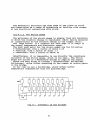
The purpose of this robot is to improve one of the numerous
teaching techniques.
A teach method is a more or less original way to record a
trajectory with the expectation that the robot will copy this
trajectory.
II.l
Method Used
A recently developed method integrates a six-axis force/torque
sensor in the robot. This method allows immediate programming of
robots either for paths or simultaneously for forces and torques
to be exerted on the robot's environment. It avoids all the
difficulties inherent with any kind of off-line or CAD
programming caused by uncertainties in the geometry of robot and
in the material to be processed. This method is based on a force
sensor, which can be used by the operator or directly placed at
the end of the robot's arm.
II.2
Other Teaching Methods
Among the several methods of teaching, in addition of the force
sensor method, three methods are predominant:
• The manual control: We use a reversible robot which is able
to be manually moved and can register a trajectory. The limit of
such a control is obvious. It is applicable solely for small
robots and accuracy of the control is also small.
• The dummy arm method: In this method, we use a mechanical
structure identical to the robot arm but not motorized and very
light weight. It includes the different position and velocity
sensors. As we use a different mechanical arm, the accuracy of
the copied motion is not as good. This method has the
disadvantage of requiring a second mechanical structure.
• The telecontrol method: The method is based on the use of a
teach-pendant or a joystick. The user can observe the effect of
his commands. The coordination of several degrees of freedom is
impossible using a teach-pendant. Another problem with the
joystick is that the human operator never masters the delay
considerations.
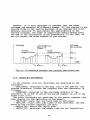
4
...
...
...
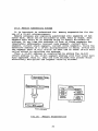
dummy
fig.!:
Teaching methods
5
III
THE R-T ROBOT
III.1
The Mechanical Part
The mechanical specifications of the robot are the following:
Translation part:
•
•
•
•
•
•
•
Maximum stroke
± 70 cm
Maximum linear velocity : 1 m/s
Maximum linear acceleration : 10 m/s2
Maximum load : 50 kg
Linear accuracy: 0.01 rom
power transmission : screw and spindle
mechanical energy provided by a DC motor
Rotation part:
•
•
•
•
•
Maximum rotation: ~ rad
Maximum velocity: ~~ rad/s
Maximum acceleration: ~~ rad/s 2
Circular accuracy: 0.002°
mechanical energy provided by a DC motor
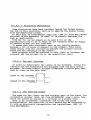
III.2
The actuators
Each actuator of the robot is driven by a DC motor ( MC 19 P
from the Electro Mechanic Company: CEM ) which requires a power
amplifier unit (Axodyn Series 05 LV power amplifier from Brown
Boveri Company: BBC).
This AXEM motor is fitted with a flat rotor with lamellar
conductors (armature) and permanent magnet (field).
This motor can also be associated with AXEM Tacho-Generators,
Brake, Gear Box and Encoder.
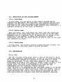
6
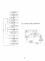
HALL EFFECT S'JlTCHES
fig.2: SCheMQ tiC of the Robot
7
FORCE
SENSDR
III.)
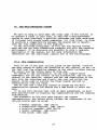
The Interfaces
Allowing the robot to communicate with the multiprocessor
system, the interfaces often limit the dynamic possibilities of a
robot. In our case we tried to design simple but efficient
interfaces.
III.).l
The Force Sensor Interface
It is not reasonable to design something for which the use and
the peculiarities are not clearly defined.
Thus, the objective of the interface must be defined as well as
the drawbacks of the original one. We must also study many
solutions and take the optimal one, which is justified from a
technical point of view and is financially acceptable.
The second part will show details and explanations to
understand how the interface works.
III.).l.l
III.).l.l.a
General Information
Justification of this Interface
An interface is very specific and has to be designed or adapted
for any need of communication between a computer and a
peripheral.
In this case, we needed to convert eight analog signals coming
from the force sensor (Refer Specific Chapter) to digital
signals. We have to carefully consider the speed of the
acquisition, the quality of the signals, the optimal use of the
force sensor, the financial investment and possibly most
importantly; give the interface many options in order to allow
for further development.
This interface has an important place in the control of the
robot. That is why, it has to be very fast, accurate and not too
sensitive to noise.
III.).l.l.b
Review of the Previous Interface
The first interface designed for this two dimensional robot
didn't satisfy to the requirements of the real time control.
It had no handshaking with the computer and the use of the
software for generating a clock rate was ineffective. Moreover,
the filter which is the guarantee of a better signal in the
acquisition chain, wasn't implemented.
8
Nevertheless we have also to consider the good points of this
interface. The use of the SDM 856 was a good idea (see in
Appendix the technical data sheets and below the technical
information), the adjustment of the offset is correct and the
decoupling between digital and analog ground is effective.
III.3.1.1.c
New Ideas
We kept the SDM 856 component, because it solves many problems
and avoids the use of three chips (Multiplexer, Sample/ Hold,
Analog/Digital Converter). But instead of using an arbitrary
acquisition directed by the computer, we decided to use the
control lines of the SDM 856, the interrupt lines and the timer
of the computer. In this manner, a lot of time is saved.
The use of a filter appeared obvious after the checking of the
analog signal shape.
Instead of amplifying the analog signal between the multiplexer
and the sample/hold it seemed more logical to increase the
amplification range of the amplifiers in the force sensor. Thus,
the settling time of the converter components is reduced and
despite the longer settling time of the sensor amplifiers, we get
a faster acquisition.
Previously if an overrange occurred one LED was lit, but no
information went into the computer. We use now an interrupt line
(Overrange interrupt) to inform the CPU of such events.
The former acquisition needed two steps. The twelve bits from
the DAC were connected to eight lines of the PPI, which meant
that we had to enable and disable the output latches of the DAC.
The output of the DAC's latches are in the new board,
individually connected to an input line of the PPI.
In the first design, the selection of the channel was done by
the CPU through the PPI. The new card owns a counter which
performs this task.
An optimal use of the force sensor is realised thanks to a
programmable amplifier. In this way, there is the opportunity to
use the force sensor as a joystick and manually applied
constraints.
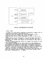
9
MTII IItAJV INTERIU'T
111 _ _
3 __
•
r
LED
I
OVERfMNGE
COMPARATOR
1
I
(1112)
L-_..J INTERRl.f'T
LED
"'7
I S/H
Allalog
Ground
IN
FILTER
GAIN stLECTl1Jf
DAC 80
COUNTER
,MIl,
FIG.31 SCHEMA TIC of the INTERFACE
10
BISTABLE
LATCH
III.3.1.1.d
Other Solutions
A more logical solution might be to use eight filters and eight
sample/hold units. in this case, the eight signals are recorded
at the same time. For economic reasons, this solution has been
ruled out.
Another solution is to use the PING-PONG acquisition which is a
specific way to run two Sample/Hold units in parallel. Thus, we
can eliminate the sampling time; because when one S/H is in the
Hold state, the other one is in the Sample state.
Analog Switch
L
I
S/H N°1
S/H N° 2
0
a-1
--0-
OJ
Input of the
DAC
Control Line
fig.4: The PING-PONG technique
111.3.1.2
III.3.1.2.a
Technical Information
The SDM 856
This component, sold by Burr-Brown is the skeleton of the
interface. It includes a multiplexer with eight differential
inputs or sixteen single-ended inputs and latched addresses, a
Sample/Hold which is also rather slow (Acquisition time: 10 ~s)
and an ADC (Analog Digital Converter) not very quick neither
(Conversion time: 30 ~s). The integration of many components into
one brings advantages, such as reliability, smaller size, less
noise. However, it is more fragile.
11
We use it in a special mode called overlap mode, that is to say
the selection of the next channel is done during the conversion
of the presently selected channel. The settling time effect of
the multiplexer, the filter and the programmable gain is no
longer included in the conversion time.
A delay and a clock are also available in this component, we
only use the delay to synchronize the signals.
The control of multiplexer's address is done with two lines
LOAD and CLEAR; the rising edge of LOAD put the data present on
the address lines into the latch and CLEAR selects the channel o.
The ADC is controlled trough the TRIG line which initiates the
A/D conversion. It runs the sample/Hold with the BUSY line.
The delay is triggered by the rising edge of the STROBE input.
III.3.1.2.b
The Filter
Also from Burr-Brown the UAF 21 is an universal active filter
therefore, it is adaptable to many uses:
• Low Pass
• High Pass
• Bandpass
• band reject
For each function, three configurations are allowable:
• Butterworth
• Bessel
• Chebyschev
And in any case we can choose the tuneable frequency, the gain
and the Q-factor.
The UAF 21 is a two-poles active filter which requires only
four resistances to be completely defined. In our application we
use it as a second order low pass filter with a bandwith of 3.5
kHZ and the Bessel configuration.
By using the equations B (Refer to the specific data sheet) we
calculate the various resistors:
• RF1=RF2= 11.3 kn
• RQ= 10.9 Mn
• RG= 200 Kn
With those equations, we must add a resistor of 11 kn between
pins 12 and 1.
The use of a lowpass filter is justified by the fact that the
speed of the acquisition is limited, so all the frequencies above
the tuneable frequency are without interest and could decrease
the accuracy of the Sample/Hold.
12
Rrt
Rf2
Mux Out HI
filter Out
71-----
RG
Mux Out LD
9
6
RQ
-15 +15
fig.5;
III.3.1.2.c
the Filter
Programmable Amplifier; AD 526
Supplied by Analog-Device, this component has digitally
programmable binary gains from 1 to 16 and is cascadable. It
provides gains of 1,2,4,8 and 16. It is complete, including
amplifier, resistor network and TTL-compatible latched Inputs,
and needs no external components.
We use only three ranges of amplification: 1,2 and 4. So, only
the three lower bits are useful.
Two modes of operation are available; transparent and latched
mode of operation. In the first one, the gain changes directly
with the level changes of the gain code inputs contrary to the
second mode which requires to select a control line (CS or CLOCK)
to modify it.
13
In our application, the transparent mode is used, so the CS and
CLOCK lines (Pins 14 and 13) are connected to the ground.
Using this component permits a wide use of the force sensor
which can either be placed a the end of the robot arm or used as
a joystick with manual control. Moreover, this component doesn't
require any Digital/Analog interface and offers very good dynamic
characteristics.
III.3.1.2.d
Offset Adjustment
This is a debatable point, because we can consider that on one
hand, this adjustment of offset doesn't bring more prec1s10n and
requires settling time. On the other hand, it seems interesting
to reduce the conversion time of the ADC.
It is realised with three components!
• a Digital/Analog Converter (DAC 80 from Burr-Brown)
• a Bistable Latch (SN 74100 from Texas Instrument) used to
synchronize the offset adjust system with the control lines.
• an Instrumental Amplifier (INA 101 from Burr-Brown) with a
gain of I, the output of the DAC is connected to the reference
signal of this component.
MUX
MUX
HIGH
LOW
I
t-----\
1------\
P
6 BITS
SN 74100 6 BITS
1------/
P t-----/
DAC 80
JO J
I
I
I
INA 101
I
Common
I
Filter
Input
fig.6: Offset Adjustment
III.3.1.2.e
Overrange Detection
Already present on the first design, this system has been
adapted to provide an interrupt signal to the computer when an
overrange occurs.
14
It is composed of one major component (LM 7470), containing two
operational amplifiers used as comparators.
with a resistor network, we select the overrange level. Each
output of the Op-Amps is connected to a voltage divisor which
includes a LED and provides a five volt level. To make this
output signal TTL-compatible we use an AND gate (SN 7432).
III.3.1.2.f
Channel Selection
A four bit synchronous up/down loadable counter (SN 74193 from
Texas Instrument) is used to select the channels of the
multiplexer. The inputs are connected to the ground and the LOAD
line is used as a CLEAR input. This counter is incremented
through the BUSY line of the SOM 856 and cleared with the output
of the timer 0 also connected to the CLEAR pin of the SOM 856.
The addresses of the multiplexer are registered by the computer
to check the data.
III.3.1.2.g
Interface Timing
In this area we allow a total flexibility, all the control
lines are put on a socket and many configurations allowed.
In any configuration, all the addresses (SOM 856 and SN 74193)
have to be at zero before each acquisition. The AOC is triggered
with the output of the timer 1 and the Sample/Hold control line
is connected to the BUSY pin of the OAC.
However, we allow many possibilities with the delay line which
could be connected to the LOAD input of the SOM 856. This delay
is adjustable from 3 to 300 ~s. The use of the timer allows the
user to select a wide range of frequencies.
III.3.1.2.h
Acquisition Speed
This is one of the major reasons for the design of a new
interface. For the first card, the maximum speed for the complete
acquisition is about 1.5 kHZ, with the new one a rate of 3 kHZ is
allowed.
We can see on the figure below the role of the sample time; the
shorter, better the acquisition is.
15
Force
Recorded Force
to t1 t2 t3 t4 t5 t6 t7
Time
fig.7 consequence of the sampling
111.4
The interface iSBCI Motor Power Amplifier
This interface is very simple and is composed of a twelve bit
DAC (Digital Analog Converter ), which is the DAC Sll from BurrBrown which provides voltage in the range of [-Sv,+sv].
In order to get the two's complemented code an inverter gate
has been used for the MSB of the twelve bits issued from the
iSBC.
The output of the DAC is connected to an Operational Amplifier
(OPA 27 from Burr-Brown), which brings the signal into the range
of [-10v, +10v] •
111.5 The position Interface
The position is coded with 20-bits, but the interface is
designed with 16-bit (discriminator) and 4 bit (counter)
components. The acquisition is achieved in two steps: sixteen and
then four bits.
The signal issued from the position sensor allows sense
discrimination. It consists of two pulses shifted in phase which
are generated by the position sensor.
Pulses issued from the Position sensor:
LL
16
The Schematic of the interface is the following:
U1
Linear
WL
Sensor
0L
U2
c
16-B1TS
Disciminator
0
4B1TS
---~
counter
M
P
U
T
E
R
fig.a: schematic of the position interface
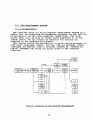
111.6 The Interfaced Devices
The Sensors are numerous in the control of the robot. One
for the registration of the forces, two for the position
recording, four for end switches. All these sensors are
interfaced to the iSBC.
To run the two motors, we also use two identical interfaces
which are connected to the power electronics.
The schematic below gives some ideas about the interfaced
devices.
17
MASTER
iSBC 186/03
Translation/Rotation
. . . . . . . . . . . . . . . . . . . . . . I. . . . . . .
··
··
iSBC
186/03
I ·
·
I
I
+
··
position
Interface
I
•
Motor
Interface
L
iSBC
II
..
..
··
····
·
I
·
·
:
Position
Motor-Power ·
Sensor
Supply
·
··
·
·
End
Switches
I
I ···
· . . . . .. . .. . . . . . . . . . ... . . ......... . . .
fig.9:
111.6.1
86/12
I
Force-Sensor
Interface
I
Force-Sensor
Block Diagram of the Interfaces
The Force Sensor
This torque sensor is a home-made sensor. It was a part of
another project and it looks like an industrial one.
The signals generated by this device have to be as "clean" as
possible, because they are at a very low level (~10 mV) and must
be amplified.
The sensor description will be divided in three parts; a
mechanical analysis, a strain gage analysis and an electronic
analysis.
18
111.6.1.1
Mechanical Considerations
The structure of this three dimensional torque sensor is in
aluminum. It has been built with two principle structures; a base
which can be mounted on the robot arm and a cover on which the
"helptool" can be fixed.
Both parts are linked together through connection bars. Six
bars are needed to ensure a static position of the two parts, the
use of more bars would be detrimental to the swiftness and the
symmetric structure of the sensor.
The main problem with the construction of the sensor is to get
the best orientation for the connection bars, because of the
small volume required for the interface.
The mechanical part consists of a circular base which is
connected to the nucleus by four bars, itself connected to the
upper ring with four bars.
On each bar there are two strain gages as close as possible to
the nucleus. Together they form a half Wheatstone bridge.
If forces or moments are performed between the two rings, they
cause elastic distortions which are converted into voltage by the
strain gages.
with the eight signals, the constraint on the sensor can be
calculated by using a transformation matrix which links the eight
voltages to the six components of the constraint matrix.
As said above, six bars are sufficient to calculate the efforts
applied on the sensor. The use of eight bars permits the
calculation of the same constraints, but as we can see in the
transformation matrix, there are many null terms. So the
calculation time is greater and the link between the two rings is
hyperstatic.
Despite the fact that steel offers a better linearity in its
deformation, aluminum is used because of its lower modiolus of
elasticity. Furthermore it doesn't corrode and is easy to tool.
Moreover, with the use of aluminum, we can get specific strain
gages.
19
fig.l0: Picture of the force sensor
20
The mechanical structure has been made of one piece to avoid
non-linearities as a cause of hysterisis or friction with screws
or non electrical connections with stick.
III.6.1.2
The strain Gages
The principle of the strain gages is simple; they are resistors
in which the relative change in resistance (6R/R) easily measured
is proportional to the relative change in the length (6L/L).
The 'Gage Factor' is a constant for each gage if it stays in
the normal temperature and distortion range.
The most used metal for the strain gages are the following:
• Nickelchrome; with a factor of about 2.25
• Platinum; with a factor of about 3.7
• constantan; with a factor of about 22
Nevertheless, it is impossible to use directly the resistance
variation of the strain gages, which is too small. The strain
gages are placed in a Wheatstone bridge to amplify the signal.
There are many kinds of bridges ( quarterbridge, halfbridge,
fullbridge), which differ according to the number of active parts
in the bridge.
In our case we use a halfbridge, which offers better
temperature compensation than the quaterbridge.
o
Ue
o
o o-+--~
Ua
o
fig. II:
Schematic of the bridges
21
III.6.1.3
Electronic Description
Some electronics have been included inside the torque sensor,
the aim of this electronic card is to amplify the signal issued
from the Wheatstone bridge.
In this goal an instrumental amplifier (INA 101 from Burr-Brown
detailed in the appendix) is used, it is exactly designed for
such an application.
With Ue= 5v, we can expect an Ua,max= 8 mv; so the
amplification has to be at least of one thousand times to supply
an optimal signal for the interface.
It seems that this electronic card is not totally perfect,
because a lot of noise is present on the outputs. This noise
comes mainly from the interaction between the printed circuit
board and the structure of the sensor.
Much progress could be achieved in this field to increase the
accuracy and the reliability of the acquisition chain.
III.6.2
The Hall switches
In order to determinate the limits of the movement, either the
rotation and the translation are equipped with two hall effect
switches. Two Nand Schmitt Trigger integrated circuits have been
used to clean up the wave form.
Input of the TRIGGER
I
\
'---
output of the TRIGGER
III.6.3
The position Sensor
The same for the linear and the circular part of the robot, the
incremental encoder (LIDA 360 from HEIDENHAIN) uses a scale tape
which can either be placed on a circular or a planar area.
This is an incremental transducer and allows the sense
discrimination. The precision of this sensor may be increased by
25 with an electronic interpolation and impulsformer (EXE 702
from HEIDENHAIN).
22
111.6.4
The Power servo Amplifier
Axodyn power servo amplifiers Series 05 LV comprise
continuously operating transistored amplifiers. The amplifier is
a multi-stage design for linearity and gain reasons. Output
current and output voltage are for optimal controlled through the
power stage in a parallel process.
The power section of the 05 LV comprises driver and power
stages. Each transistor is provided with its own emitter
resistance to improve current distribution and the symmetrical
arrangement allows the unlimited four quadrant operations
This device includes also a speed regulator which is a tacho
control, but it isn't used in our application.
r-----~----~~------~------~-------O
+
UQ
V control
V control
- Ua
~-----+-----4~------~------~-------O
fiq.12:
Power section of the Axodyn Power Servo Amplifier
23
IV
THE MULTIPROCESSOR SYSTEM
We have to keep in mind that the final goal of the control is
to operate a robot in real time. In this way a multiprocessor
system or more precisely a parallel processor has been developed,
it includes four single board computers, all from Intel, in order
to maintain a compatibility between the boards and to benefit
from the long experience of the supplier.
In the following paragraphs, we will see the various boards
used and the way they communicate together and with the hardware
environment. It is obviously not possible to give a complete
description of the system, but for more information the
references for the individual reports are in the bibliography.
IV.1
The communication
This is one of the most crucial parts of the system, since we
use many boards to share the operation of the control, as well as
the fact that the effective command to the robot includes knowing
the actual and the future state of this one.
As stated in the introduction, we use four single board
computers; one for the control of the translation, one for the
control of the rotation, another one for the acquisition of the
data from the interface and finally the last one called the
master, which used to control the other boards and has no
communication with the robot.
But we also use a multibus system to establish the data
communication between the boards and a RAM board to store the
data.
It is now more obvious that with so many subsystems, we have
many possibilities to organize the communication and the computer
architecture.
The schematic on the next page explain the system
implementation, but before going further the references of the
various boards must be given:
•
•
•
•
•
Master computer: iSBC 186/03
Translation computer: iSBC 186/03
Rotation computer: iSBC 186/03
Sensor computer: iSBC 86/12
Ram board: iSBC 028A
24
RS 232
TERMINAL
PARALLEL MUL T1BUS
MUL nsus 8MHZ CLOCK (10 MHZ optiOno.D
AR1JITRAGE CONTRll..
u-t
fig.13:
:IV. 2
Posttlon
L/R HALL switch
u..
POSItion
f'CJ«:E/HOMD£NT
(f'x,f'y.Mx)
System Architecture
Multibus System
IY.2.1 Definition
The multibus system requires a great deal of effort to
understand completely. The multibus system is a standard of
communication introduced by Intel in 1986. It is also known under
the name of IEEE 796.
This bus architecture is the conceptual foundation and physical
framework for interfacing the various components of the Intel
family. This family includes single board computers, memory
expansion boards, a broad array of I/O expansion products,
packaging products, microsystems software and integrated
microsystems.
It contains all the necessary signals to allow the system
components to interact with one another. This system is based on
the Master-slave concept. The 'Handshaking' protocol between
masters and slaves allows computer of different speeds to use the
multibus interface and also allows data rates of up to five
million transfers per second. The multibus system bus can support
multiple master device on a back plane and can directly address
up to 16 megabytes of memory.
Its interface structure consists of 24 address lines, 16 data
lines, 12 control lines, 9 interrupt lines and 6 bus exchange
lines.
25
To sum up, the multibus interface is included on each single
board and could be seen by the user as a parallel interface,
needed only proper configuration before use.
IV.2.1
The Multibus arbitration
For the multibus arbitration, we use a parallel priority
resolving technique which uses a separate bus request line
(BREQ) for each arbiter on the multi master system bus. Each BREQ
line enters into a priority encoder which generates the binary
address of the highest priority BREQ line which is active.
The arbiter receiving priority (BPRN true) then allows its
associated bus master onto the multi-master system bus as soon as
it becomes available. If a higher bus master is requesting the
bus it has to wait for the present instruction to be finished.
However a lower bus master can keep the multibus by using the
lock instruction which disables the other masters to use the bus.
There are two other ways of arbitration:
• The serial arbitration: The BPRO (Bus Priority out) of each
master bus is connected to the BPRN line of the next priority
master bus.
• The rotational priority resolution: This technique is
similar to the parallel resolving technique except that the
priority rotates. This allows each arbiter an equal chance to use
the multi-master system bus.
-
NClI
"
-..
""
"""_11
"
.........
,.
.."
r
-----
L
-----
I
N011:
-----
----
.
.............
-
«'0W£$1)
"
--
-
----
wu fOmTMGMDIIIKtlltl
0dAIl1tfG OIIHlO/OUTPUY.
fig.14:
Parallel Arbitration
26
1:g1C~1
ItllOnOM)
_J
IV.3 ThQ RAM Memory Board; ISBC 028A
The iSBC 028A random access memory board provides a dynamic
memory storage capacity of 128 K bytes. This RAM memory
interfaces directly with the bus master via the multibus
interface in any 8 or 16-bit ISBC operating board .
• Access time:
read
write
--> 500 ns max
--> 343 ns max
• Cycles times : Read, Write and Refresh in 608 ns max
This RAM board is used to store the common data; forces,
moments position registered, position calculated •••
IV. 4
IV.4.1
Single Board Computers
iSBC 186/03
The iSBC 186/03 is a general purpose, 16-bit computer system on
a multibus-compatible printed circuit board. The board supports
the high-speed memory execution bus (iLBX bus) for local memory
expansion. The board is designed to interface to the small
computer interface (SCSI) with some reconfiguration and some
optional components.
The specifications of this single board computer are the
followings:
• iAPX 186 (80186) high integration microprocessor
with a speed of 8 MHZ.
• iAPX 86/30 (80130) operating system processor.
• Eight byte-wide memory sites for EPROM, EEPROM,
SRAM, iRAM, or NVRAM.
configurable memory capacity: up to 32K bytes of
RAM and up to 256K bytes of ROM memory on the
board.
• iSBC 341 memory expansion multimodule board
compatible, expanding RAM to 64K bytes.
• iLBX local memory expansion for high-speed
transfers to/from iLBX memory expansion board.
27
+ 27 interrupt sources on-board using the 80186,
+
+
+
+
+
80130 and 8259a interrupt controllers and the
8274 serial controller.
Two serial I/O channels controlled by an 8274
multi-protocol serial controller (MPSC).
General purpose parallel interface: can be
configured to the SCSI or Centronics interface
by adding PALs.
Two iSBX bus interface connectors.
Master capability.
Dedicated front panel interface connector.
After this short introduction, the user could find more
informations in the iSBC 186/03 single Board computer Hardware
Reference Manual (Order Number: 146414-001).
IV.4.2 iSBC 86/12
We will examine this single board computer more in detail,
because it is directly used for the acquisition of the
interface's data.
It would be difficult to explain the choice of the 12 board for
this particular use, because it was the responsibility of
previous stUdents.
The major quality of this board is the Dual Port RAM, this RAM
is either addressed by the CPU and another bus master controlling
the multibus. So the communication between the CPU and the other
single board computers can be done without stopping the CPU. Any
device can put the data in the Dual Port RAM which can be
accessed at any time. In this particular use, we call the iSBC
86/12 a slave RAM.
The iSBC 86/12 single board computer is controlled by an Intel
8086 16-bit Microprocessor (CPU). The CPU includes four 16-bit
registers that may also be addressed as eight 8-bit registers.
The CPU contains also two 16-bit pointer registers, two 16-bit
index registers, four 16-bit segment registers.
The CPU instruction set supports a wide range of addressing
modes and data transfer operations, signed and unsigned 8-bit and
16-bit arithmetic including hardware multiply and divide, and
logical and string operation.
Four Ie sockets are included to accommodate up to 16K bytes of
ROM.
28
The iSBC 86/12 provides 24 programmable parallel I/O lines
implemented by means of an Intel 8255A PPI (programmable
peripheral interface) chip.
The RS232C compatible serial I/O port is controlled by an 8251A
USART (universal synchronous/asynchronous receiver/transmiter)
chip from Intel.
Three independent, fully programmable l6-bit interval
timer/event counters are provided by an Intel 8253 PIT
(programmable interval timer) chip.
concerning the interrupts the CPU has non-maskable interrupt
(NMI) and maskable interrupt (INTR). The NMI interrupt is
intended to be used for catastrophic events such as a power
failure that requires immediate action of the CPU. The INTR
interrupt is driven by an Intel 8259A PIC (programmable interrupt
controller) chip which, on demand provides an 8-bit identifier of
the interrupting source. This 8-bit identifier is multiplied by
four to provide a pointer for the interrupt service routine.
PARALLEL
110
SERIAL
110
(MULTl8US)
(AUXILIARY)
fig.15 intel Single Board Computer 86/12
29
IV.5
Memory Addressing Scheme
It is important to understand the memory segmentation for the
use of a 16-bit microprocessor.
Memory adresses are logically subdivided into segments of 64K
bytes each, which can be allocated to code, data or stack. Each
segment must start at an address which is evenly divisible by
sixteen. At any time the contents of four of these segments are
immediately addressable (current code segment, current data
segment, current stack segment, current extra segment). Since the
effective address of a 16-bit microprocessor is being 20-bit and
the segment used is only 16-biti we must use an other 16-bit word
called offset to calculate the address.
Thus, a 20-bit address is constructed by adding the 16-bit
offset address to the 16-bit segment address with four lower zero
bits appended. That is, they are left shifted four places which
effectively multiplies the segment value by sixteen.
'5
I
0
12~~lns
lOGICAl AODIIESS
"----
ti
fi_fGMENT II£GIST[~
0
100 0 ol~tGMENT
A DIIUS
IMPLICIT
SELECTION
r-
CODE
STACK
DATA
~
EXTRA
~D;Y
SEGMENT
REGISTERS
~~S~£G~M-t-NT""'I1
+J18gAl~~
I
201fT
PHYSICAL
ADDRESS
How." Addt... I~
!L
I
D
2O·81T
'HYSICAL MEMOIIY ADOlIlSS
I
M.1ItMJ Addt........
fig.16:
Memory Segmentation
30
'.,1It
I
1
V
THE SOFTWARE
This is a very important part for proper operation of the
interface. We will see the software development, the structure of
the program and explore different parts of the software.
It is unnecessary to explain in detail the program. The user
is left to examine the program listing and documentation.
V.I
Program Development
At the beginning, we didn't know if the software should be
written in assembly or in pascal, as both languages have
advantages and drawbacks. It appeared more useful, quicker and
easy for the debugging to write a first version in pascal.
In any event, it will be easier to implement an assembly
program by using the algorithm of the pascal one.
Learning to use the Pascal 86 took little time, and the time
was more often spent on configuration problems (PPI,PIC,PIT) than
on the specifications of this language, which was quite close to
the standard pascal.
We intended to do a program as modular as possible, in order to
allow further development.
Many problems came from the use of the monitor IAPX 86-88 which
wasn't adapted to the interrupt of the intel Single Board
computer 86/12. The use of the iSDM 86 Monitor V 1.0 solved all
these problems.
The last logical step was the simulation of the interface which
showed the limits of the software. The maximum speed obtained was
about 10 KHZ.
V.2
Program Structure
As explained in the previous chapter, this program has been
built in four modules.
The program itself called MAIN; calls the routines of other
modules, set the interrupts and runs the acquisition. This module
contains also the interrupt routines which was initially put in a
separate module.
31
flg.17: FLO'JCHART & MODULES COMMUNICATION
..
L
CONS
/
...
..
"'"'
)I
:(
Module
JI"
'\.
HARD
Module
(
MAIN
.....
PPI
PIT
.
...
Module
~,..
n
IINTERF ACE I
' - lNTERl
Module
force-sensor
,~
--"
32
The module used for all the public declarations needed in the
multi-module structure is called INTERl.
The hardware initialisation modules (PPI,PIC,PIT) is named
HARD.
To facilitate the communication between the operator and the
computer we introduced a module under the name of CONS.
The idea of using an interface module (INTERl) is useful for
the development of the program. A change in data only requires
the change of the interface specifications.
In the future, the communication between the computer and the
operator should be run by the master, meaning that the
communication module would be suppressed and the data should be
read at a specific address in the RAM board.
V.3
Calculations
We have many way to do the calculation, but it is obvious that
we have to consider that the acquisition is not continuous. Many
algorithms permit such calculations, but as a first step we use
an easy one; a linear interpolation. The precision could be
increased by using a most powerful method (higher level of
integration), but this better precision would be to the detriment
of the system speed.
Voltage
Uc:used to calculate the forces
Calculation time
Time
to
tl
fig.18: technique of calculation
33
However, it is also important to consider that the eight
voltages are measured at different moment. So, the chances to get
results close to the reality decrease if we consider the first
channels selected. To equilibrate the approximation of the
various voltages, the order of acquisition should change after
the end of the calculation of the constraints. in our case, we
can not change the order because of the counter.
Voltage
~C~lCUlitiOn
Tl.me
Former
Acquisition
Last
____A.9<llli§!.tJ-Qn_
Voltage
Calculated
U8,C
TIME
fig.19: differences between the various approximations
V.4
interrupt procedures
In our program, only two interrupts are generated by the
interface:
- DATA_READY: connected to the busy line of the SDM 856 (see
chapter interface) informs the computer that the conversion is
finished.
- OVERRANGE: connected to the overrange detector of the
interface, it is set if one of the analog signals is out of the
range [-lOv,+lOv].
The other interrupts are generated by the master computer (see
next chapter for the definition of the modes):
- TEACH INT: means that the teach mode is activated.
- TEST_INT: Occurs when some tests of the interface, the RAM
board or the various computers are done.
- REPLAY_INT: starts the replay mode.
- SAMPLE INT: generates the sample time for the acquisition.
34
V.S
V.S.1
Definition of the Various Modes
Test Mode
In this mode, all the parts of the control system may be
checked; the RAM board, the interface, the counters and the DACs
(counter and DAC from the rotation and translation interfaces),
this mode is not always used but might prevent many troubles if a
improper operation of the robot is detected.
V.5.2
Replay mode
When activated, this mode makes the robot copy the trajectory
registered in the teach mode. The robot is able to do the same
movement even if a greater force is applied on it; which is the
objective of the method. We teach the trajectory without
constraints and then the robot should be able to move in the same
way, whatever its load.
V.5.3
Teach mode
In this mode, the teaching method already defined is used, the
force sensor is obviously used to record the path.
V.6
V.6.1
Peripherals
PPI
The PPI includes three ports (port A, port B and port C) which
offer many possible configurations. It has 24 I/O lines which may
be individually grouped in 2 groups of 12 and used in 3 major
modes of operation. In the first mode (mode 0), the lines are
programmed by group of four Input or output lines. In mode 1, the
second mode each group is programmed to have eight Input or
output lines, the four lines remaining are used for the
handshaking and the interrupt control signals.
Only the port A is affected by the last mode (mode 2), it allows
eight lines to be configured either as Input and output, that is
to say bidirectional lines. Five other lines are used as control
lines borrowing one from the other group.To programm the PPI,
only the writing of a control word into the 8255A is required.
35
PORT Are
K
K
PORT C
(lower)
PPI
PORT C
(upper
8 higher bits
fro!'! the DAC
3 o.cldress bits
4 lower bits
froM the DAC
6 bits for the offset
PORT B
fig.20:
V.6.2
+
2 bits for the go.ln
Configuration of the PPI
PIT
A timer is a very useful component to generate a sample rate or
a simple clock without involving the CPU.
The Intel 8253 is organized as three independent 16-bit
counters, each with a count rate of up to 2 MHZ.
The counters may be either programmed to count in BCD or in
binary.
Each counter can be connected to one of the three clock rates
available: 153.6 KHZ, 1.23 MHZ or 2.46 MHZ. We have also the
possibility to connect the output of one counter to the clock of
another one.
A gate allows an external device to trigger the counter if this
one is so programmed.
Five modes of operation for each counter are programmable by
the software with simple I/O operations. The three counters may
be programmed individually at any time, It requires a control
word and a count value for initialisation. Usually consisting of
two bits, the count value may be reduced to only one: MSB or LSB.
Mode 0: Interrupt on Terminal Count. The output will be
initially low after the loading of the control word and stay low
until the terminal count is reached. This occurs assuming that
the gate is connected at a '1' Level.
36
Mode 1: Programmable One-Shot. The output will go low on the
count following the rising edge of the gate input and remain low
until the terminal count.
Mode 2: Rate Generator. The output is initially high, then it
goes low for one cycle. The process then repeats.
Mode 3: Square Wave Generator. high during on half of the count
and low during the other half. for odd count the output stay high
for (N+l)/2 of the count and low for (N-1)/2 of the count.
Mode 4: Software Triggered strobe. The output will go low for
one clock period after the terminal count which is initialized by
the loading of the counter.
Mode 5: Hardware Triggered Strobe. The counter will start
counting after the rising edge of the gate input and the output
will stay low for one clock period at the end of the count. The
counter is retriggerable.
V.6.3
PIC
The Intel 8259 handles up to 8 vectored priority interrupts for
the cpu. It is cascadable for up to 64 vectored interrupts.
The 8259 is designed to minimize the software and real time
overhead in handling multi-level priority interrupts. It has
several modes, permitting optimization for a variety of system
requirement.
To use this device two types of command words should be
defined; the Initialization Command Words CICWs) and the
operation Command Words (OCWs).
ICW1 indicates if that PIC takes place in a multi-pic
configuration or not and defines the level or the edge
triggered input for the interrupts.
ICW2 gives the address of the first vector interrupt.
ICW3 is only used for a slave PIC and indicates to which master
interrupt it is connected.
ICW4 defines whether or not an EOI (End Of Interrupt) is
generated and if the Fully Nested Mode is used (Interrupt
requests are ordered from 0 trough 7).
Concerning the Operation Command Words, only OCW1 has to be
clearly defined because it sets the interrupt mask. The others
can be forgotten in most of applications.
37
V.7
The development system
V.7.1 Presentation
The Intellec serie III micro-computer development system is a
useful tool for designing microcomputer software for the IAPX 8688 processors. We can write programs, debug them, link them,
locate them and run them on single board computers or on the
system itself. We can connect an emulator for running our
programs in the hardware environment.
This system offers the possibility to write source programs in
high level languages: Pascal, Fortran, PLM and Assembly. These
languages are special Intel's versions (PASCAL 86, FORTRAN 86,
PLM 86, ASSEMBLY 86) which are quite close to the standard
versions.
p--_.....-..
_ _ _ _ _ _ _' O.£ . . T,IOO:
....
S'SUM ,
• LOolOEA ,
1._------"
r·--·
.. •· ..
, OfllUGOEA :
1
OR
t
: _______
1I0lO,TOII J•
..
•.------- ..•
• 'N-CIRCUIT •
: _______
EMULATOl!:
1.
"
.
,,._.----,
1 - _.....:
CREFN
..
I
:
:
•r------:
USN"
·
•
OH"
I
:
•
1---.I
•L_--
"---l---"
•
-_....... _,
r-------,
I~::~--------------~
:.-------.1
:
•
HEX
LOAOEA
fig.21: Drawing of the System Development
38
:
I
• ........ ""' •• J.I
I.
V.7.2
Compiling and Linking operations
The Pascal 86 compiler is very powerful and efficient, it
generates a file with the same name than the module compiled, but
with the LST extension.
The interface module can not be compiled alone, nevertheless it
is compiled with all the other modules.
The Linker is also a powerful tool to link all the Object
files, as well Pascal or Assembly object files. However, the
linking can not be done without using the libraries required.
The files P86RNO.LIB and P86RNl.LIB are both always required,
when using real number, the file 87NULL.LIB is necessary and the
use of several modules involves the file RTNULL.LIB.
After the linking task, the object file has to be located: the
DATA segment, the STACK segment, the CODE segment and the
starting address must be defined.
Then, the located file can be converted in an HEX file to be
put in an EPROM or to be downloaded from the development system.
39
VI. CONCWSION
The management of a project abroad is totally different from a
project done in our own country, because in addition to the
technical work there is the every day life which requires an
adaptation and some changes in our habits.
Most of Dutch people are fluent in English and German, so the
communication is always possible.
The technical work was interesting, not very new for me, but
anyway it was a good experience.
One of the major problem was the fact that many students have
worked on the robot, and some of them didn't reach satisfying
results, so their work had no conclusion. I wanted to avoid such
a situation, that's why I wrote a report as complete as possible
to allow any further development. The conclusion on my work are
not easy to reach, because the interface wasn't tested in real
conditions.
However, I'm very optimistic regarding the performance of it.
The atmosphere of working was pretty good, and the other dutch
students helped me a lot for my integration among them.
I improved my English a lot and I discovered a country which is
really oriented to the foreign countries and well prepared to the
future European Common Market.
40
APPENDIX CONTENTS
Appendix
I: French Summary
Appendix
II: Practical Informations
Appendix III: Schematic of the Interface
Appendix
IV: SDM 856
Appendix
V: UAF 21
Appendix
VI: AD 526
Appendix VII: INA 101
Appendix VIII: DAC 80
Appendix
IX: SN 74100, SN 74193
Appendix
X: Motor, Power Amplifier and Encoder
Appendix
XI: Listing of Main.src
Appendix XII: Listing of Inter1.src
Appendix XIII: Listing of Hard.src
Appendix XIV: Listing of Cons.src
Appendix
XV: Listing of Location File.
Appendix XVI: References
41
Appendix I
RESUME EN FRANCAIS
Durant ces cinq mois, j'ai apporte ma contribution a
l'elaboration du control d'un robot qui comporte deux degres de
liberte (Rotation et Translation). La finalite de ce robot est de
repeter des trajectoires enregistrees prealablement.
L'originalite de ce robot consiste dans l'utilisation d'un
capteur de force tridimensionnel qui est precisement utilise pour
l'enregistrement des trajectoires.
Mon champ d'activite s'est surtout situe au niveau de
l'acquisition des efforts appliques sur Ie robot et mesures par
Ie capteur de force. A cet effet, j'ai con9u une interface ainsi
que Ie programme qui la gerait.
Mon travail s'est deroule en plusieurs etapes; au depart il m'a
fallut acquerir certaines connaissances sur Ie robot lui mame,
ensuite je me suis occupe de la conception de l'interface et
finalement de la mise au point du programme de gestion de
I 'interface. Le programme a pu etre teste dans de bonnes
conditions, mais l'interface ayant ete achevees trop tard, je
n'ai pas pu effectue tous les tests requis. Mon travail sera donc
conclu par un autre etudiant; j'ai donc apporte un soin tout
particulier a la redaction de mon rapport.
Ce travail n'etait pas d'un niveau technologique et
scientifique tres eleve, mais la necessite de communiquer en
Anglais, de lire des articles en Anglais et de dependre d'autres
services apportent des difficultes qui s'estompent peu a peu,
mais restent malgre tout un obstacle a la conduite de projet plus
consequent dans un temps limite.
Sur Ie plan personnel, ce stage a ete une experience tres
enrichissante; decouverte d'une autre culture, amelioration de
mon Anglais, mises en pratique de connaissances theoriques et
surtout eveil a un esprit international.
Appendix II
PRACTICAL INFORMATION
1. Use of SUBMIT program
This program allows the user to create a file called batch file
which may prevent to compile, link and locate all the files
separately. This BATCH file is called BATCH.CSO in our example
(see following page). By this way, if some modifications are
brought to any modules, the user don't have to wait that one task
is finished to start the following one; he has just to run the
SUBMIT program with the syntax below:
SUBMIT :FX:BATCH.Extension(Name1,Name2, Name3, ••. )
Fx is the drive where the BATCH file is put
Name1,Name2, •• are the source files.
In our example, we only use three source files, but the batch
file can run with five source files. As we can see on the listing
some lines start with ';' separator; this means that the line
won't be interpreted by the SUBMIT program.
2.
How to start the program?
with the iSDM86 Monitor, a located file is required to be
downloaded from the system development to the single Board. For
this task a program called iSOM86 is supplied by Intel, but the
various operations have to be done in a certain way.
The transfer of the located file requires the same baud rate
between the system development and the Single Board, so when the
iSOM86 file is activated, then the Single Board has to be
reseted. When the Single Board is ready, it print on the screen:
iSOM 86 Monitor, V1.0
Copyright 1983 Intel Corporation
Then the file can be loaded in the on board RAM with the
instruction: L:Fx:Name.STA
x being the drive where is the file
Name is the name of the file
STA is the extension given the batch file (see previous
chapter). When the monitor is ready, it prints '.' on the screen.
The program is able to run till this moment, the instruction
'G' performs this task. To stop the program, the 'CNTL C' Key can
be used. Then the 'G' instruction starts the program again or the
'E' instruction permits to the user to Exit the current program
and return to the ISIS-II environment.
~file:BATCH.CSD
·._---------------------------------------------------------------,•
,·
.
I
I
I
COMPILER & LINKEn & LOCATER (& HEXCONVERTER)
.
•
•
•~
I
I
I
•~
II
,•
I
•
I
,•
I
•
I
•
I
Put
,,
·,·
in drive 0 de systeemdisk,
in drive 1 de pasca186floppy,
in drive t1 de program.
---------------------------------------------------------------
I
I
;*****************************************************************
;*
Compiling of the source files
*
;*******************~*********************************************
RUN
:F2:PASC86 :Fl:%O.SRC
:F2:PASC86 :Fl:%l.SRC
:Fl:PASC86 :F4:%2.SRC
~:Fl:PASC86 :F4:%3.SRC
;:Fl:PASC86 :F4:%4.SRC
'*****************************************************************
*
linking of the object files
;*
;*****************************************************************
L.INK86 ~.;
: F4: ~~O. ODJ ~ : F'l: :(,:1., OB.J:
F":
;:F4:%3.obj; :F-1-;;~4.Dbj, ~~
J
:Fl:P861:~N().LI8~
:
i~2.
:F:l.:PB6r~:Nl.L.rB,
OBJ,
: F4: %2. !.JB,J,
~:I.
S~
:Fl:87NULL.LIB, :Fl:ce187.1ib, ~
:Fl:SDMIOL.LIB, :Fl:MBUS86.LIB, :Fl:SBCIOS.LIB TO :F4:%1.LNK
:Fl:RT~~LL.LIB,
:*************************~***************************************
;*
locating of the link file
*
;*********************************~*******************************
LDC86
~<
: Ft1: "1.1.
Un:::
TO : Fi.!: %1.. ST(")
~-.:
INITCODE (1000H) &
ORDER (CLASSES (CODE, DiHA, STACI-:::»
81,
ADDRESSES (CLASSES (CODE(1400H)~ DATAC2400H), STACK(3400H»)
;*******************~***3.****************************************
*
;*****************************************************************
;* INITCODE,ORDER and ADDRESSES have to be compatible
;********************~********************************************
;*
;*
CONVERSION to HEXA-DECIMAAL formaat
creation of a file with .HEX extension
*
*
;*****************************************************************
; DH86 l!1.
~:F4:%1.STA
TO :F4:Xl.HEX
Appendix ]I
7
8
+1SU
+1SU
A-
1 __~~__-'r-__~--'----r--~------------------------------------------------------.+SU
1
.---I
__
__
__+-__4-__-+__ ____,,__ __
__
__________________.+lSU
cA-~
D
1
2
3
5
6
~-+
~~
~
~
~-'
--r---~----------
c-~ ~
A-30 __~-+--~~--+---4----+--~----4---+---~-1----~--+---~---'r---r---~--~----r-._1SU
C- 30 ~
2
2
2
1
2
2
2
2
2
11
L J1
~ ~ ==1 -~ Cl::- C't
-c:tc y
C
J
C
C6 _: CT,
C~:
c*,
Cl":: CiT,
I
~~~ ~lrI_' I_'~::':::jf::::Jt:':::1L:':::~:2:::JL:'::I:1::JL:'=t=~=:~I~N_JL_'
~
L.L=-~
__66~SlH rom.,...
1-~"""'--______.:::68"1S1H IN
l.JLIyLtIllX_________'!!2~ ttJX
XU
=
•
X1 5
4CW
8
DO
~
~
X14
X16
I~
REF
Al
A2
I1JX EN l/A3
a...!XX RATE
I::....------------:=1ej'~8 '-"'"
~ EHa.£
~
~<41
mU01
D( 6 )
010
39
n, '"'
011 <40
nr" \
~nt..
"
,
EHU...E 2
~
5"/.-,
R8
oc:
-15V .....
~
"~
L
-
14
-
u
-
-{bs~
S
OS08
<4
~
OS08
~
0508
10
•
8
.J..
"C?l
" CR ,
c-
R«'
"' ?l
\.OJT
OJ<
.--1--+-=-18
~"" , =,
~r
9~
'..J
fG()2
r--!LOGW
____
F6{}
___
+SU
+llSU
" CQ
,
011
-i..JljR~C:°8"t=
:~~80~~"
1
r-~-',,·'-!OSO
~DBl
03
-I__-,~ :,x:LS37 3
____
RCO'
B(1)
8C 2'
813l
8C4l
I • • OS
~ LS32
3
01
<4
D2
7
03
8
D4
13 os
eAIN ADJ
~DB' 5U". J ""C ~
~DS3 zo u SI" AN ~
!.!......
Qlt~?e~."~n":t1-1~:f~
:5 ~:~
r.( .. \
U OUT
~
"""
008
DB.
VnEF Il<
0010 VREF OUT
e,?,
04'"" ,
Q3
6
QS
12
ct.'
"'" <
ct?, •
r
+lSU -lSU
SU3
Z3"-'-"2
10V SPAN
"8(5)14 0606 '50c"
...12.."
+SU
itA:;;
:~
l-----
SUl
r---+ os...
Q2
~
At
5
eccc-
12
13
1'"
15
16
17
18
19
B
20
21
2'"
2S
D- 26
~
__~
R19
D- V
28
02
J R20
cc-
TNH
TIMERO
22
23
D-8
"
~---I
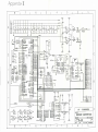
TU - EINDHOVEN
R21
~
R22
PROJECT
R23
S8£OR INTERFACE
~
~U'lA<~~,~"'~;;::::=~;::::===~3!!S~0~7.11 g . 23
"ca"OOl1
L____~C=.D="""=HJ.,,''------I
4
c-
'1
+15U
TEX .
. 1ooc . ~ .
C'I
J89003WiT .
JVK
I
6
DD-
11
llSU
•
7
~
CDCCDC-
tULI-4
I
r-
011'
U IN
~~
~ os
rl ~
~9 - 15V
S8&f'8,-,--,f"-'~
IINe,
AC'"
1
~-10
LS32
OS08
-;;-
(FT.2 ':'"
ACS'
DC Q ,
H..LL tt=:::{i~n:::::J
0' 15 AO
~
P2
, 7_____ ~
2
+V
"""
n C•• ,
T4
~~~~
OS
LS32
3
-
011
~
05
0508
____~
0-2
c- 3
0-4
0- 5 "
0-.
C- 7
C- 9
D- 10
"' n,
~
.u. .
~
0
FRE~~~2Uu
13 : --++SV
'---~+--_--+'~2"'
--
L-.!..!.
~8~=:l----!l
~O
Jg
-~ "
L-
6 6
10
OUT~3C===1f!-em
7
FREQ . A' .
aM1£><
~5"b
J~~~~~~~~~~~~--~~~9~!:~~:::7:7::::::::::::::::::::J-................
~
>..1...L
roo
IJ'
LP
C
+lSU
1
foP WT
~
em lSAm
em f.i~~~U
emp'
em &
SlN/Orr
Q
----~S9 ~
0:Q1-Sl.J.l:!
,,)E~32
L------------------------------"'"-l~?
7
<4
EPO "S9"'------4-J,
*
A2
14 I>FVT2
N'VT3
OIG . a::t1f2"'-------t--......
S
TII1ERO
---.g
G
"
DSl
1O-aIT
RES
011 OJT
UAFll
12
em~ss~==:ttl--!Eg::}----'
e-eIT RES
EHa.£ 3
~ 011 rn::a..£
.-1++--'"
</'-j0El.AY ADJ.
+lSU ___+-I-~6 +V
~ DFVTl
CELAY emf-i4"S-----1H----------'
a...!XX
r.Pl--l
"1
>"-----'!~I<RSn!.-,
-is
J>m
36
37.lll
"'
-lSV
-lSU
~
3S - -~
os
-6.4'-'
SfmT CYU.E
1
r
lN~l'48
-
Z2 a
10 _l!V'""c6'
-<J/
~ ~ ~an~
.-I-+-~'" TRlE
t
4
AO em 17 AC 0 ,
16 :A, 1)
IN
IN
IN
22 A3 IN .
--=
50
23
~:
D _.
REF ~ 57
Q-U3IRETS
",,4/RET6
OilS/RED
~'--------;o21~A2
n
lR121+Ul
03~ 3334 ",""i:
0709
QU2IRET4f
1-''--______~19;.JAO
i--''-______,,20~A1
9
.~ -:;. "'--
29n .'nl
01 ;:
D2 32
06
73 "'QUl/RET3
' IRE1"2
Xl0
X12
4
'~4
5 -
-0(""5")
n
X6
A-2
OS08
C~,
l@a""
2N'2
...rr ~7D8-------t+-t-------"-f.:.~;".
0l1T Ul r------_t-t-J
5 0i6
)(8
D
INT]
:j'3
____
-{j4
2
OJT
~~~71
71° Qf3IRETO
Di9lRET1
X2
X4
3
lN~l'48
74C
--i
6 2
SlH em ~
SlH 0F"FSf:T -"'-
O<S
X13
1
"0'
HSU -
43 cu
BVSV Ift,;.,'-4------_to
SDM 856
01
7 "'4
X9
C~
V2
BVSV
I'1JX
I'fJX
Xl ::=:mCHO
>C3
l~ail
~
If____J_
*
EN 2
11
d :2
10
2
20V RA<i£
1 DU RR'I3E ~
n_~ BVSV ..-..:
Vi
.~~
Cl~ Cl.f. Cit Ci~I Cllt Cl7T, C18
+Sl.OC f;4f-9-.+su
-ls.oc
1,
_____
j[2 __l_f2___JL
_2____2___
___
~~~~~t==16S~+l5VDC
: : ANA 001
I.
1,
3
2
1
ttBJ89003
0
CTDEE
~"6
~1;
o[::::::25
~!
00000000000000000000
>s>&
00000000000000000000
o-oo:J-oQ
[
&~~0::oOI::::::8
[
01
00000000000000000000
'?i'?i
mooooooooooooooooooo
~4
IIOtIlOt
o
~
o
0
ij (;;J ~
55 35 o~o :-t=-o C:: ::'5
i 809 0t:l~
I::::: ::s Co I::::::~ (r ( : : : : ::3$
~
0
U1
B
3
0
I::::::: :!:S
o-t:B2IJ-o
"6~
~w
~O7.119.23
o~o
o-ma:::J-o
I::~c:::::::~: :<
IIOtC12
..
o-iBIID-o o-£Bi2}-o
o-I::Ri3J-o
o~o o-[Bffi-o
t;Jt;J
0
0
0
CO
-0
0
0
0
0
0
0
0
0
0
0
0
0
o0 A
0
0
0
0
0
0
0
0
0
0
0
0
0
0
0
0
0
0
0
0
0
0
0
0
0
0
0
0
0
0
0
0
0
0
~ o· r:::::::'5
0
0
0
0
0
0
o
~~
32 32
••
•
Appendix N
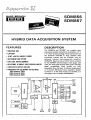
SDM856
SDM857
BURR-BROWN@>
I' •• ·1
HYBRID DATA ACQUISITION SYSTEM
FEATURES
DESCRIPTION
The SDM856 and SDM857 are complete data
acquisition systems contained in a miniature 2.2" x
1.7" x 0.22" ceramic package. These systems offer all
the functions available in large modular data
acquisition systems and are available with an
optional internal instrumentation amplifier
(SDM857). Inputs as low as ±IOmV can be accepted
by the SDM857; thermocouples, strain gages, and
other low level signal sensors don't require external
signal conditioning. Both models are fully
expandable from the basic 16 channel single-ended
or 8 channel differential input capability. Digital
resolution is 12 bits with accuracy of ±O.024% at a
throughput rate of 29kHz (SDM856KG).
- MINIATURE SIZE
-LOW COST
- 12·BIT. to.012% LINEARITY ERROR
-INSTRUMENT AMP OPTION
- LOW LEVEL INPUTS ISOM857)
- SELECTABLE 16 SINGLE. 8 DIFFERENTIAL INPUTS
- THREE·STATE OUTPUT BUFFERS
- THROUGHPUT RATES (SDM857 Overlap Mode)
8-Bit Accuracy: 70kHz
lO·BIl Accuracy: 32kHz
12·Bil Accuracy: 29kHz
SIH
Outputs
Inpul CDnirOIOuipul
rn~put'
- -OiiipUi1
Analog
Inpull
I
I
I
I
I
I
I
•
I
I
I
I.A.
-
Inpul r _ _ _ _ _ ___oSerl.1
Dall
r~.....l _ - - - - - - - ( ) Stalus
and
Cunlrol
,
I
I
I
L!~~~.!!_~
Olgltll
OutpUll
Enabl.
L~~::8} Oulput
lines
Sirolli
Clock
R... Adj.
_.". ....
Clock
Oul
-.,~"
---
Relerenc.
OutpulS
~."'."."
,.",.,"-" . . . . . .
r."
"""'~"'"
... '
,. ... ""
.
111---',.''''''''''
. - - " ..... Oulput
...--..:;.... (UIU 1
Oil
010
lit
DB
...----='--4 (U.Ul
01
06
IUh
All CAlMrill'
CHIIIlll'
ClltI1lETI
tHIOI1llU
CHIIIMT3
CHI2IMU
CH I311m
CHI4/1ne
QlI"lm
.UX UIAILf "
A20UT
A30UT
AIDUT
AO GUT
0$
D4
D3
or
DI
10
>-=~:: lrtAlLfl
L~~==~'t:', : ..in;IV(III[[
!i§~§~~Rn
_.1-..-.... l~~~~~~~~lI!r ...n
SHORT
CYCLE
S(IIAlIUr
III.SOlUTIDI
lIun .£SOlUTIDI
AOIII
AlII
A211
A311
12
.UI
SIIII DELAY 11101£
EMAILl r DIf ADJUST
IIfLAY TlIS
OUl
FIGURE I. SDM856/857 Block Diagram.
SYSTEM PERFORMANCE
SDM856 and SDM857 are configured for random
channel selection. With the addition of an external
counter they can be configured to continuously sequence
through all analog channels or sequence through all
analog channels on command from an external trigger.
With the appropriate 4-bit (singJe-ended) or 3-bit
(differential) channel address on the latch inputs, and
DELA Y OUT (pin 45) tied to the LOAD input (pin 23), a
negative going edge is applied to the STROBE input (pin
48). This starts the delay timer. latches the multiplexer
address, and allows the input signal to pass through the
multiplexer, instrumentation amplifier and sample/ hold
and settle to its final value before starting the A/D
conversion. The DELAY OUT signal (pin 45) is also
connected to the TRIG input (pin 46) and the A/ D
conversion is initiated on the negative-going edge. The
StH CONTROL input (pin 66) is connected to BUSY
(pin 24) so that the sample/hold is in the HOLD mode
during the AID conversion.
By using overlap programming the settling lime effects of
the analog multiplexer and instrumentation amplifier
can be reduced, extending throughput sampling rates up
to 29kHz for 12-bit and 70kHz for 8-bit resolution (ADC
short-cycled). This mode of operation is most useful
when converting low level inputs to accommodate the
increased settling time of the instrumentation amplifier.
Overlap programming is accomplished by connecting
BUSY to STROBE and StH CONTROL; DELA Y OUT
to LOAD and T"iITG. In this mode of operation the
address of the next channel to be converted is latched and
the output of the instrumentation amplifier allowed to
settle to a new value dLJrin~ the rresent conversion.
DIGITAL INPUT SPECIFICATIONS
Addr~'
InpUIS
One >!andard l.STIl load.
po~;t;ve
tfUI.'
(AO· A3)
Addrc., Codin,
4-bit binary
LOAD
Onr sl~ndard I.STIlload. po;ilive true,
pO .. IIH cdge.
addr~',
loaded on
Onc standard lSTIL load. negal;\'r trLl(. 10..' Incl clear.
addre", latch.
STROBE
One "andard lSTIl load. high.to-Iow Iran,ilion triggcr.
the dela)' limer,
One .Iandard I.STIlload. a negali\( going I.'dgr iniliate. the
A.O comer.ion.
SHORT CYCLE
Onc 'Iilndard I.Sn'l load. logic I for l2-ml resolulion.
Connect 10 ~8·bil· or MI()'bil- for II· or I()'bil roolulion,
ENABLE I.
ENABLE 2,
ENABLE 1
One 'Iandard I.STII. I"..d. a 1o.. k\c1 cnabl!:, Ihe
IiTi ENABl.E } 3·.1,,1< OUlrul.
BUSY ENABLE
SIH CONTROL 1'11. compalit>lc. IO/'A muimum inrul ("urrcn\.
I.,,~ic 0 " 1I"ld mode. 1,1I1t" I
Samr'" (lrarL) mode.
MUX ENABI.E 2 I'll cumra!!t> ... 2/,1\ input currenl. I uj1ic 0 enah"',
mulhrlcACr 2 (oannel, ti·I~I,
DIGITAL OUTPUT SPECIFICATIONS
"arallrl 1>011 ..
()Ulr Uh
S<'llal OUlrUI
2 .... nd .. 'd 111 'n~d•. ,,",;Ii,( Irue. ~K/. hme "·,,.. 1 d"la
nulrul t>cl'"m",., ",Ib 1>11
I uII'nj:
im
5 .... nd~'d
."'<
n
0,,,.,';11,,1
I I"ad•. r'''lli\c Ime . .1-"alC,
tiUSY
5 .I"nd.. ,d Til luad_. I.." dUlifilt A U (nmr"'un
BUSY
Cl.OCK OUT
5 " .. "d.ud 'I II, I""d,. IUj(h dUflll1.! A J) C"Il\~",un. J->Ialc
~ .Iand... d 111 I.... d •. lUI ,)n(hWnllill~ ""li,,1 uul d"l"
(,ecl.m'IIJ l>til!! ... m),
Add. f" Oulruh
(AU· A.'.
5 I.S n I. I... d., IH"'ili,c true
m:I.AY OUT
S ""nd.,d n'l, 10lld•• hillh durin/! dtillY period. lfiIlIlC.<,d
t>y Slrut>c inpul.
SIN/OIF
5 I.STII.lold •• hilh .. hilt .dd.fujnl ct>annel> 0.7,
ItI'" "'hll. addrc"in8 eh.nnt!. M-15,
Appendix'Sl
UAF11
UAF21
au"" . • •
IEIEI
UNIVERSAL ACTIVE FILTERS
FEATURES
APPLICATIONS
• SAVES DESIGN TIME
• FILTER CONFIGURATIONS
Uaer·tunable 'requency, O-factor, gain
Calculate anly three ralltanee valuBI
Dllian directly from thll data Ihell
Compillely chlrlctarlz.d plramllen
• IMPROVED PERFORMANCE
Wide 'requency rlnan
UAFtl • 0.001 Hz to 20kHz
UAF21 • 0.001 Hz to 200kHz
1% fraqu.ncy accuracy
Qrange of 0.5 to 500
Butlerwartlt
BIII.I
ChabYlchev
• FILTER FUNCTIONS
Low Pili
High pa••
Bandpasl
Band raJect
Rlllibl. hybrid conatructlon
NPO clpacllon Ind thin-film rellaton
DESCRIPTION
The UAFll's and UAF21's are low cost universal
active filters. These versatile units can easily be
tailored to any active filter application using the
extensive information provided in this data sheet.
UAF's are excellent choices for use in communications equipment. test equipment (engine analyzers.
aircraft and automotive test, medical test. etc.). servo
systems. process control equipment. sonar and many
others.
The UAFll's and UAF21's are complete two-pole
active filters with the addition of four external
resistors that provide the user easy control of the
Q-factor, resonant frequency and gain. Any complu
filter response can be obtained by cascading Ih"f
units. Three separate outputs provide low-pass. hi~!>.
pass, and bandpass transfer functions. A band-r(jw
(notch) transfer function may be realized simply ~\
summing the high-pass and Jow-pass outputs.
Since these UAF's are so versatile and nexible. the~
can be stocked by the user in quantity for u~e a'
building blocks whenever the requirement ari~e<
This means instant availability and the UAF pur·
chases may be made in volume to take advantage (I!
quantity price discounts.
'IIjIIIU
oAdjust
Iftterllllltntl AIrpwt IRftstrlll PI"'· P.II. au 114l1li· T-. am..1M. TIL II1II 7..1111 • Tft 1I1J.1&Z·1111 • CIIIII: IBIU:8IIP· TIIt.:"'1
Appendix~
Software Programmable
Gain Amplifier
AD526 I
r.ANALOG
WDEVICES
ADS26 PIN CONFIGURATION
FEATURES
Digitally Programmable Binary Gains from 1 to 18
Two-Chlp Cucade Mode Achieves Binary Gain from
1 to 258
Gain Error:
0.01% max, Gain = 1. 2. 4 IC Grade)
0.02% max, Gain = 8. 18 (C Grade'
0.5ppmrc Drift Over Temperatur.
Fist Settling TIme
10V Signal Change:
0.01% in 4.5p.$ (Gain = 18'
Gain Change:
0.01% in 5.6.,.. (Gain'" 16)
Low Nonlinearity: % 0.005% FSR max (J Grade'
Excellent de Accuracy:
Offset Voltage: 0.5mV max (C Grade'
Offset Voltage Drift: 3.,.Vrc (C Grade'
m Compatible Digital Inputs
DIG GND
At
1
AO
CS
VIN
ANALOOGND2
AD526
eLK
TOP VIEW
(Not to Scale'
A2
ANALOOGND 1
-Vs
VOUT SENSE
B
+V.
VOUT FORCE
PlOOUCT DESCRIPTION
The AD526 is a single-ended, monolithic software programmable
pia amplifier (SPGA) that provides gains or I, 2, 4, 8 and 16.
II is complete, including amplifier, resistor network and
APPUCATION HIGHUGHTS
I. Dynamic Itanp Exteasion for ADC Systems: A single
AD526 in conjunction with a 12-bit ADC can provide %dB
TTL-compatible latched inputs, and requires no external
alIDpOnents.
2. Gaia RanciDl Pre.Amps: The AD526 offers complete digital
of dynamic range for ADC systems.
gain control with precise gains in binary steps from 1 to 16.
Additional gains of32. 64. 128 and 256 are possible by cascadiDi
two AD526s.
Low gain error and low nonlinearity make the AD526 ideal for
precision instrumentation applications requiring programmable
pin. The small signal bandwidth is 350kHz at a gain of 16. In
addition, the AD526 provides excellent dc precision. The FETinput stage results in a low bias current of 5OpA. A guaranteed
maximum input offset voltage of O.5mV max (C grade) and low
gain error (0.01%, G = I, 2, 4, C grade) are accomplished using
Analog Devices' laser trimming technology.
To provide flexibility to the system designer, the AD526 can be
operated in either latched or transparent mode. The force/sense
configuration preserves accuracy when the output is connected
10 remote or low impedance loads.
The AD526 is offered in one commercial (0 to + 7O"C) grade, J,
and three industrial grades, A, B and C, which are specified
.
from - 40°C to + 85 QC. The S grade is specified from
55"C to
+ 125"C. The military version is available processed to MIL·STD
8838. Rev C. The J grade is supplied in a 16-pin plastic DIP,
iIId the other grades are offered in a 16-pin hennetic side·brazed
ceramic DIP.
(
I
.
Appendlx~
BURR-BROWNe
INA101
I' I' II
MILITARY ,. DIE
VERSIONS
AVAILABLE
Very-High Accuracy
INSTRUMENTATION AMPLIFIER
FEATURES
APPLICATIONS
• ULTRA-lOW VOL TASE DRIFT • o.Z5p Vlot
• lOW OFFSET VOLTAGE· 25pV
• LOW NONLINEARITY· 0.002%
elOWNOISE-I3nV/v'ifz atl.= 1kHz
• HIGH CMR • 106d8 at 6IIIz
• HIGH INPUT IMPEDANCE· 10100
• lOW COST. TO-100. CERAMIC DIP AND PLASTIC
• AMPLIFICATION OF SIGNALS
FROM SOURCES SUCH AS:
PACKAGE
Strain Gaga
Thermocoupla
RToa
• REMOTE TRANSOUCERS
• LOW LEVEL SIGNALS
• MEDICAL INSTRUMENTATION
DESCRIPTION
fhe INAIOI is a high accuracy. multistage, inte,rated-circuit instrumentation amplirier designed for
lignal conditioning requirements where very-high
performance is desired. All circuits. including the
Interconnected laser-trimmed thin-film resistors, are
Integrated on a single monolithic substrate.
A multiamplifier design is used to provide t he highest
performance and maximum versatility with monolithic construction for low cost. The input stage uses
Burr-Brown's ultra-low drift, low noise technology
10 provide exceptional input characteristics.
OFFIET ADJUST
OFFSET ADJUIT
-INPUT
GAIN
SENSE I
8AIN lET!
+Vcc .Vee A2 OUTPUT
M Package
_11110lIl1
G and P Packages
Airport lllduslrial hrII· P.O. Be. 11400· T _ Am...134· '11.l1l2I141-1111 . Tn IIlllZ·lIn . cal.: BBRCORI'· Ttln: 66·11491
A
endix-.szrn
BURR-BROWN.
DAC80
DAC80P
I' II II
AVAILABLE IN
DIE FORM
Monolithic 12-81t
DIGITAL-TO-ANALOG CONVERTERS
FEATURES
•
•
•
•
•
•
•
•
•
•
INDUSTRY STANDARD PINOUT
LOW POWER DISSIPATION: 345mW
FUll ±lOV SWING WITH Vee = ±12VDC
DIGITAL INPUTS ARE TTl- AND CMOS·COMPATIBlE
GUARANTEED SPECIFICATIONS WITH ±12V AND
±15V SUPPLIES
SINGlE·CHIP DESISN
±1I2LSB MAXIMUM NONLINEARITY. oct II +700C
GUARANTEED MONOTONICllY. GoC II +70°C
TWO PACKAGE OPTIONS: Hermetic lide-brazed
cerlmlc and le.-cOlt melded plude
SETtliNG TIME: 4,11 mix II ±D.01% II Full Sell.
DESCRIPTION
This monolithic digitat-to-analog converter is pinfor-pin equivalent to the industry standard OAC80,
first introduced by Burr-Brown. Its single-chip design
includes the output amplifier and provides a highly
stable reference capable of supplying up to 2.SmA to
an external load without degradation of 0/ A
performance.
This converter uses proven circuit techniques to
provide accurate and reliable performance over
temperature and power supply variations. The use
of a buried zener diode as the basis for the internal
reference contributes to the high stability and low
noise of the device. Advanced methods of laser
trimming result in precision output current and
output amplifier feedback resistors, as well as low
integral and differential linearity errors. Innovative
circuit design enables the OAC80 to operate at
supply voltages as low as ±1I.4V with no lou in
performance or accuracy over any range of output
voltage. The lower power dissipation ofthis 118-mil
by 121-mil chip results in higher reliability and
greater long term stability.
Burr-Brown has further enhanced the reliability of
the monolithic OAC80 by offering a hermetic, sidebrazed, ceramic package. In addition, ease of use
has been enhanced by eliminating the need for a
+SV logic power supply.
For applications requiring both reliability and low
cost. the OAC80P in a molded plastic package
offers the same electrical performance over temper·
ature as the ceramic model. The OAC80P is available
with either voltage or current output.
For designs that require a wider temperature range.
see Burr-Brown models OAC85H and OAC87H.
For designs that require complementary coded deci·
mal inputs. see Burr-Brown model OAC80-CCO-V
(-I).
-t---..---Relerence
Gain
Adju$tment
,----Scaling
H~~..,..........._-Network
Analog
Output
Ollset
'---_ _ _ _ _ Adjustment
--+Supply
---Supply
'lIIII'allllllll Airjllft'lIduIIrlll PIrk· P.II.11D 114011· Tuu-. am..114· '11.II1II1.1111 . 'wa: .....·HI •. Callie: "ICOIIp· T....: II·HlI
TTL
CIRCUIT. TYPES 5NS47S, SNS477, 5N54100, 5N7475,SN7477, 5N74100
8·BIT AND 4·11T BISTAlLE LAtCHES
tTl
aSI
SNli4nlSN7C71
SNli4l1ISN14l1
W fL ... T PACK"'OI!
ITOPVIEWI
JOR N OUAL·lt....lNI
OR W fLAT 'ACKAOIITOP VIIWI'
151
CIRCUIT TYPES 5N54192, 5N54193, SN74192, SN74193
. SYNCHRONOUS 4·ln UP/DOWN COUNTERS (DUAL CLOCI WITH CLEAR)
o
•
Cascading Circ:ui1ty Provided Internelly
•
Synchronous Operation
•
Individual Pr_t 10 Each Flip-FloP
JORN
DUAL·IN·LlNE PACKAGE ITOPYIEWI
»
-0
.'-0
•
fully Independent Clear Input
•
Typical Maximum Input Count F,equency .• , 32 MHz
C1)
TRUTHT....LI
................
... ....,
description
0
D
1
•
_
'_ .......
1
•
....- ....
_
, NOTU~ i t. ~. bit tliM: "NI. ~
SNli41001SN14'OO
JOR N DUAL·IN·L1NE OR W fLAT PACKAGE 1T000VIlIWI'
_ " ' -........ _ ...n.
2.
-
Thew monolithic circuils are synchronous reversible 'up/down)
counlert ha.ing a compl.xity of 55 equivalent galH. The
SN54192 and SN14192 ar. BCD counters and lhe SN54193 and
SN14193 are 4·bit binary counlers. Synchronous operation is
provided by hiving all flip·llopo clocked simultaneously 110 thai
the outpull change COincidently with uch other when 110
ill$tructed by the Steering logic. This mode 01 operation
eliminates the output counting spikes which are normally
associated with ••vnchronouslripple·clocl<l counters.
t".,...............
·.tt .......... .
clOGk
..NC-'" ....,.......MCtloft
.
_
..... : LowlnpullO 10""0" 0 ........
0a • a o 0c • c, ond 00 • 0
~
The outputs of the fQUl' master·1Iave fllp·flopc are triggered by a IOW·10·high·levei IT_ition of either count Iclock
input. Till direction of counting is determined by which count input is pulled while the other count input il high .
,
.....Ipdon
TIIeII IItdIII
All four counters are fully programmable; IhItt is, .... oulpUlI may be pr8i8t to any Slata by entering .... desired data at
IhIt dati inputs while the load input is kM. Till output will change to agree with the dati inpul5 ~tly of the
count pulses. This feature allows the count_ 10 be used as modLllo·N di.idets by limply modifying the count length
with the pr_ inputs.
IN ....Iy lUiud tor
~ IIklI'III for binIry
....
I nfoI'mIItion bII.wMn proc:eMlg
unI'III .... Inputlautprt or lndlcltor
unItI. Intorntlon ...-c III • dete
IDtI...................... O
GUfPUI wt.t ... cIoc:& .. h/eh.....
' . 1M Q outprt will foIIgw 1M dele
~. Input . . . . . . 1M dodI rtmeiIw
lilt .1. III
. h/eh."'" 1M cIoc:& . , . kM. 1M
;. • ......mMiorI.1MI _
pr_ III
eM deta Input" eM tlnw eM ....-....: _ _ _
1t'IIIIItion 0CCiIIrNdI .. NhinId III
::mI~tput ~
cIoc:& It L.I'In-............
- - - , - . , -...
-_-...
- ...-,....
- ....
-._--...
- ..
- , - _ - _ - - - - - - - - -......
j
,
1------------------...:.----1
, ._......... ...
:J
CL .
X
A deer input has been provided which fO(_ all outpull to the kM level when a high level is lIPPiied. TIll clear function
is independent of the count and load inpull. An inpu1 bufler hat been placed on the clew. count..... load inpu1I to
low« the drive requir_U 10 one nor....tiled Seri<l$ 54114 load. This is impo<tant ~ .... output 01 .... driving
circuitry is somewhat limited.
OUIpu_
Ttiese counters were designed to be aIICoIded without the need lor external circuitry. Both bomIW and carry
..e available to ~e both th, LIP' and down-counting functions. The borrow output produces • pu .... equal in width
to the count-down input when the countet underflows. Similarly. the ctIIry output produces. pulll equal In width to
the count·up input when an o_flow condition exllts. Till counters can then be easilV c.cadId by feeding the bomIW
and carry outputl to the count-clown and count·up inputs respectively of the succeeding counter .
"
TIll SNl47&I&H7475 f _ ~ Q .... U oulpUts from • 4-bit 1D:h..... II ....... in eM 10iJin
........ For ..... oompooIIftt deMIty appIIcationI .... SN64771SN7471 4-IIIt latdt It _il... in . . 141J1n filii
........ TIll SN541001SN14100 _ _ _ \ndIpIndInt quadruple IatdlIIt in.1infIIe 24"" . . .-In-lina .......
n- cIrcuIU . . cornpINIy compatible with all popuI.. TTL or OTL .amlllIL TypicII ~ dIIIipatIon It 40
mlllIwatU ......... n. &erieI 54 cin:ults IN c:harIcWimd for .,atlon __ 1M full mIIIwy .......,...,.. I'IInII of
....C to lWC .... SerMi14 dn:ullllN c:Nrac:ttlf1md for GpllIItion from O"c to NC.
lbIoIutI mlXimum,1ItingI ( _ ~ ........... ,... l1li1_ o1hlrwite noad)
Supply VoIuue. Vee (See Nota 31 ' , . • • • , , ,
'. . VoIuue. Vin IS. No_ 3 .... 4, ' . . . , . ,
Operating F....AIr Temperature R. . . : SN6415 Circuits
SN7475 Circuiu
NOT6-a: 3. n... .a.... vaIIH&.,. witt'! ~1: 10 MiWCWk .,Of,mel 1IttM .......
4. •. . . , . . . . . 1ft.... be UtO or pOlJdve wtlh . . . .' to MlWOflf. II'OUnd -..mln...
Power dissipation is typically 325 milli..-tts for eid\et the decade or binary version. Maximum input count frllQUll\CV il
typically 32 megahertz and i. jUa<antlled to be 25 MHz minimum. All inputs are buffered and represent only _
nor....lized Sari<l$ 54114 load. Inpul clamping diodes lire provided 10 minimize tran&mission-line effectl and thereby
limplify syotem design. Till SN54192 and SN54193 are characterized 10( operalion over the lull militery tamper.ture
range of -55'C 10 125"C; the SN74192 and SN74193 are characterized lor oper.tion from O·C to
mOe.
absolull maximum rau,. _
•
.
'IV
, , • , , 5.5V
, -55'C to 125°C
O"c to NC
-6fj·C to 15O"C
operatilllJ free..ai, temperature rafllJ8lun_ otherwise notedl
Supply IIOltage Vee 1_ Nota 11
Input voltage 1_ Nota 11
......
...... .
. . . . ..
...... .
Operating fr",·1ie temperature range: SN54192 and SN54193 Citcuits
SN14192 and SN74193 CiteLlits
Stor8g8 tamperaturerange . . . , . . . . . . .
.
7V
1i.5V
-55·C 10 125"C
. o·C to
-6fj'C to !WC
mOc
Appendix X
Power amplifier
Axodyn-Power Servo Amplifier 05 LV 05
B.B.C,
Brown Bovery company
Table 1 Summary of Speclnc.tlon
A.oayn
Type
Orde, No.
GJV160 ...
Supply
Voltage
Power
Conaumption
VA
V
05lY01 ... -e
OSlV02 ... -E
05lV03 ... ·E
05lV04 ... ·E
05lV05 ... ·E
05lV06 ... ·E
OSlV07 ... -E
05lVOB ... ·E
OS LV09 ... ·E
(J)
... 1001 R1
... 1002R1
... loo3R1
... 1004 R1
... 1005Rl
... 1006R1
... 1007 R1
... l008Rl
•.. 1009 Rl
Output
Power IUPplift
power ,,'vo amplifier
220V/1220V/1220v/1380V/3380V/3220V/1220VI1220V/l220V/l-
200
250
550
1200
1200
500
400
550
550
d. c. voltage d. c. current Dynam'peak Output
curr.n~J)
impedance
rating<2I
rating':!)
A-
V~
±13
±24
±52
+ 80/-12
±45
±40
±24
701-12
±24
et ,eted d, c. current
II> c:.an be aOIU$ted Irom 10'l0 to 10m. of rated d, c, current
± 8
.± 6
± 6
±10
±20
±10
±10
± 6
±15
Power
ratln",!)
A-
D
W
±16
±15
±15
+30/-20
±40
±20
±20
+ 151-10
±30
0,30
0.20
0,30
0,30
0,30
0,30
0,20
0,30
0.25
100
145
360
800
900
400
240
420
360
Dynam·
peak
pow.,
W
weight
210
360
780
2400
1800
800
480
1050
720
6,0
8.5
18,0
37,0
37,0
18,0
10,0
18,0
18,0
(3.
mall 2l1ec, decay time constant can be aet
",1
reduction 2'I'oioC from 40"C ambjentlemperatur8 Increase
kg
\
Table 2
RegulaUng and Control Section
Techo control
OperaUng rangu
Adjustment range
Control range
Control error
Tolerance of connection voltage
Frequency
Guaranted temperature range
Operational temperature range
+ 10%-10%
50 ... 60 Hz
OOC ... 400C
from -100C ... +SOOC
atabillaed CUI'1"aftt aupply
poaltive output voltage
negative output voltage
Temperature drift
max. additional loading
1: 5000
±0.5%
IR CompenNtlon
Actuating range
Control range
Control error
10 ... 100%
1: 100
±5%
+14.1V... +1S.9V
Current limiting
(specimen scatter)
Current limiting (continuous current) 10 ... 100%
Dynamic peak current
see table 1
Malt. duration of dynamic peak
current
see Fig. 11
-14.1V... -15.9V
< 2.25mV/oC
±20mA
Note
8peecI regulator
Rated voltage
Actual voltage
malt. eltt. rated voltage
Input resistance rated value
Large signal gain
In--phase suppression
Limiting frequency (without network)
Offset voltage adjustment
0 ... 100%
± 15 V
The limits of the control range are associated with the
. permissible control error. Indication of errors is related to
rated output voltage (speed) and the following interference variables; a wider control range is possible with
a larger error:
± 15 V
± 30 V
30 kO
200000
90 dB
10 kHz
by potentiometer
Change in load
Mains Yoltage fluctuation
Temperature change
58
4: 1
±10%
±5%
I:S I:S ~ ~=ii2""·'-VL.IIL.i\I~U u.~.
BROWN BOVERI Rotterdam TeL:010·180 280
E' P A RV E X
21·29, rue Lucien Juy. 21001 • DIJON·CEDEX • fRANCE
o£pt VITESSE VARIABLE
Phone (10, 41.11.1' - Telex 350653
MC 19 P
SYMBOLS
1
'1.
-
MOTOR RATINGS
Rated Torqu••
12. Rated Sp.ed ..
13.
....
15.
16.
17.
18.
Ulell'"
(I)
Rat.d Output •
Rated Voltagl.
Rated Current.
Maximum at Very Low Spe.d •
P"I,. Torqu. lintermittent operation I (3)
Maximum Speed with no external load ..
Cn
Nn
cm.N
r.p.m.
Pn
Un
W
In
Icc
Cimp
Nmax
V
A
A
cm.N
r.p.m.
Me 19 P
Cool.ll m
10 lifel/sec
16,5
2440
510
3000
1600
87
22,2
22.3
2440
5000
5000 ,
320
3000
1000
83
I ......
• S,all molOf ; ask I/S for "'alt. curt.llt
• • Fo. other dl/lr CYCles : &$1\ I/S
2
-
MOTOR CONSTANTS
21. E.M.F.lIOOO RPM..
ke
•.
Kr
KN
22. Torq". Constant/Ampere ..
23. R.gulatlon Conrotant Voltoge/cm.N
2... friction Torqu. .• .. .. ..
25. Damping Con "on' 1 1000 RPM .•
26. T.rmlnol 'e,islance f4l.,
27. Armalure Inductance., ..
. 28. Total Inertia ..
29. Mechanical Tim. Constant
2.10 Pow.r Rot. (i)
*,
,
3
I N
8
....
..
!.
.-;-
!
...... \_.
. § ......
I
t'oI
JI
2.'.
te
•
E
..
'l'~'
Q,
J
l'
p,
0
0,3
10
8
0,46
#lH
g.cm2
m,
12000
9.2
KW/s
500
<100
PERFORMANCE CHARACTERISTICS, CONTINUOUS OPERATION
i
••c
KO
R
L
25,S
24."
parallel loyer,
-
iii
Tf
V
cm.N
'.p.m.
cm.N
cm.N
".,.,.
---:
\
.!:
j
r
..
•12
.
!
I
I
- I ..
In.
I
!._J ...
I
i..tt'
'''T'' .
~ n-
201
i
j ..
.
i
.'
I
~~
!
-..•
.i-.
I
·1
I
~
! .....
.. .....-
:
1
.. -. .. .
"- .
'1-
'e
.
-
.~
--;-
r--,
.. !. .
"'1-;' r-'"
N
, .,.. ....~
~
I
,,- ~
I
..
-
iI
!
. ....;
.
.. .. -
I
'T"
I
-1'-
i
I
600
410
:
... ,.
i
i
~ ~ r-+~ .-.~
i
..
;12
!
,
:
;
.\h.
. I ..•
.•.J...
~
\~ .. !"-.
" ;.!.\IiJ
'-1- .. !=M. ~
1
·-i.·~·
I
!i
~I
I
100
Torque (em. N)
0 ....
!iI''''" af'
1ft
pfac1u:a indepen"'"' Of lhe a,mall/,e tampe,alu,e
11 Mount,ng on malll plaia ••llIlhelmall",ulalion I 401h400k10 mm'. and puf. DC lupply. Amb,.nl ,_pal'llil/" O' C 10 40' C
J)
Lou '" ",otOI : 13 "'''' 01 H20
;) I A.._d eyela 5:1.
~
mi. I X
.. I Value '"Cludad 10101 pllII cont.a '''''Ianca .II,cll doe..
HI(; .....' ..tIe1l conlut ,a.j.tance a.c •••sell
5) Calculalacl from III. lormull:
I Pul •• lorque I 2
fr
:t,
ftCII ..alY
••111 alma, ..." I.mpe ••' .... ~Ince oI'mlt".e "'s,stanc.
25.5
24.'"
0,3
10
8
0.46
<100
12000
9.2
500
_
==
WinkelmeBgerat
Inkrementales offenes WinkelmeBgerat
mit AURODUR-Stahlband
Teilungaperiode 100 fJrYl
MeBschritt bis 0.000020
8endauflagedurchrraener il: 600 mm
...........
~.-:""
.. •..
. . ",:'" '"' '.
... .,.
~!;'
,
......... .,.. ......
:
.
, ..... ,,: ,..;..\-....... ';~.;.f;'.', ",.- '.: .
• fIo...
.....,
".
60
HEIDENHAlt,
LIDA 36(
yom
Bandauflagedurchmesser (0) .. da Teilungsperiode des AU~OL
.bhangig
Stahl-MaBbandes immer ,OO~
(omm + 0.3 mm) •
z - Int [
01
. mm
Int: Ganzzahl-Anteil des in Klammern stehenden Ausdrucks
Strichzahlen [z]
Bandauflagedurchmesser
:s 3000mm
MaBband-Teilstucke
Stahl-MaBband-Teilstucke konnen uber Spannschlosser miteinander verbundt
werden.
Wlrmeausdehnungskoeffizient
des AURODUR-Stahlbandes
In der Mine (Toleranzbereich ± 10 mm) des Stahl-MaBbandteilstOckes und d..
ausgehend im 5O-mm-Raster.
Damit die erste und letzte Referenzmarke nicht ntiher als 5 mm am Stahl-Ma.
band-StoB liegt wird der Toleranzbereich von ± 10 mm ausgenutzt.
Referenzmarken
MaBband-Genauigkeitsklasse
±5~
GroBter Unterteilungsfehler
± 2 J.IITI (± 1 ~ nur mit EXE 700 nach Abgleich)
± 5 ~ an den StoBstellen
zulissige Beschleunigung
zullssige StoBbelastung
Schutzart
Abtasteinheit staub- und spritzwassergeschutzt nach IP54 (DIN 400501
Korrosionsschutz
Abtasteinheit: eloxiertes Aluminium
Stahl-MaBband. Spannschlosser und EndspannsWcke: rostfreier Stahl
Arbeitstemperatur-Bereich
Abtasteinheit: CP C bis 450 C
Stahl-MaBband und MaBbandtrager: CP C bis 5CP C
Nur wenn der MaBbandtrager aus eioem Material besteht. dessen Warmeau~
dehnungskoeffizient zwischen 9 . 10. 6 und 12 . 10-6 K- 1 (z. B. GuBelsen oder
ferritischer Stahl) betragt. Bei hoheren Warmeausdehnungskoeffizienten (z. B
Aluminium) gilt ein eingeschrankter Temperaturbereich von 100 C bis 300 C.
lagertemperatur-Bereich
Abtasteinheit: - 3CP C bis TCP C
Stahl-MaBband und MaBbandtrager: CP C bis 500 C
relative Feuchte
max. 80%
Gewicht
Abtasteinheit
350 9
SpannschloB
300 g
EndspannstOck 300 9
Stahl-MaBband 60 g/m
Sektrilche
~nnwert.
± 10%. < 120 rnA
Lichtquelle
LED mit Vorwiderstand: 5 V
Impulsformer~lektronik
a) in zahler eingebaut
b) extern. siahe EXE-Druckschrift
Ausgangssignale
Inkremental-Signale 1.1 ~I\I\J\
•
1.2VVV\
•
t--,..............:=
•
Referenz-Signal
110
SignalgrbBe
1.1 ca. 11
1.2 ca. 11
fJAu
1.0 ca. 5.5 J:iA~
I
2 anntihernd sinusformige Signala 1.1 und 1.2
1 Signal 110 pro Umdrehung
bei Last 1 kOhm
- Nutzantell
HOchste zulassige Drehzahl n.....
n
max
(min- h
J
_
f!!llx 1kHz) • 103
Z
•
60
z: Anzahl der Teilungsperioden von 100 J.IITI auf dem Umfang (Strichzahl)
f.....: maximale Eingangsfrequenz der e)(ternen Impulsformer-Elektronik
zulassige Kabellange
lOr
FoIgeelektronik
20 m (HEIDENHAIN-Kabel [3 (2 x 0.14)
61
+ 2)( 0.5) mm2 )
Appendix X[
,'1PUULE PH I NC I r'u:::;
{*
{-lJ·
This module is th~ !lp.?rt of the progr;",m, i t includ~.;'s .3.11 the
r-outines to f~!J.n t.he .?Ctiui.sition and the calcule.tir.m (J'(' the
*}
*)
{* constraint.
This module calls also procedures from othpr modules.*}
C* This progr~m doesn't do the adjustment of offset, 3t the e~d of
*}
C* module a flowchart is given in this way.
*}
$INCLUDE (:F4:INTER1.SRC)
fhe :inclusion of II'nE:J:;:1..'3F'C: alloltJs this module to use the
declared in INTERl.SRC and to call the other
{* proredures and functions declared as public.
f*
C*
v~riabtes
$INTERRUPT
(TEACH_JNT~0,RFPLAY_INT=1,SAMPLE_INT=2,TESr_INT=5)
$INTERRUPT(DATA_READY~6,
DVERRANGE=7)
PROGRAM PRINCIPLE;
COt;J::·n
DELAY',::!O;
PROCEDURE. ASSIGN_INrr.RRUPfS;
{-~
{~
This; procech'.n2 a:tr-i.I1I.I.tr,:~s the levf.?l of the di·f+erpnt intc?rnJpts
used, i t al~o permits to define the interrupt vectors.
*}
*>
BLGIN
DISABLEIN"fCRRUPTS;
{*Disable the interrupts at the CPU level.*}
!3ET r NTEF~F:I.JF'T «(lOC II, TEr-)f~;H .._ I NT) ;
SErINTERRUPT(001H,REPLAY_INT);
SET I NTFRPUPT (O(,,'f-L, S,;H1PLE_.I 1\11 ) ;
SETINTFF;:f~Upr (OfX::iH~f):3T"".Il'rrl;
SETINTERRUpr(0~6H,D0TA_READY);
SET I NTEF:F<U!'']' «('Ull-!"
O\lE.F<Fu~t'.JGE ~
ENAHLEINTERRUP1S:
C* Enable the interrupts at the CPU level. *}
;
elf 'The procE'dLlr·~s -fnllm'linq !:ire c:allf.?d ItJhf"n the h,:;'lrr1"Jart:"
{* interrupts connected to the PIC are activated.
PROCEDURE TEACH INT;{*This procedure services hardware interrupt O.*}
BEGIN
PRINT30('Teach Interrupt Activated
TEACH::::::TRUE;
');
F.ND;
PROCEDURE REPLAY
IN1~{¥This
procedure services
hard~are
interrupt 1*}
BEGIl',1
PRINT30('Replay Interrupt activated
');
HEPU·,Y: =TRUE;
END;
PROCEDUF:E SI:\t'1PLEU'H, f.*Thi s pn:lcedure services han:h·;are interr-upt 2*}
BEGIN
PRI~~IT·:3t.)(='Sample
S{~t'1PLE:
Irft:el.... rLtpt. Act:i'/ated
=');
::::TF:UE;
END;
PROCEDURE'TEsr INT:{*rt,is procedure services harrlware interrupt 5. *}
BEn I 1'.1
PRINT30('lest Interrupt Activated
TESTl.:==TRUF;
ErtD;
PROCEDURE DATA_REAOY;{*This procedure services hardware interrupt 6*}
BEGIN
DATt~:
::-::TRUE;
Et··m;
PROCEDURE
OVEf~RANGE;{*!his
nEG I ",f
CO ( , IT ) ; CI )( " (.r
) ; CO (" E'
procedure services harware interrupt 7. *}
) ; CO (' R' ) ;
OVEH:=THUE;
END~
{*****************************************************~************}
{~***********************************************.*****************}
PRUCEDURE CALCUL_VOLTAGE;
{* The TEMP_VOLTAGE
matrix calculated in the main program is
{* used to determine the VOLTAGE matrix.
VtiR
I~,J~t~U-)X_COEFF,DLmiAL
:
*}
*}
INTEGER;
BEGIN
MAX_COEFF:=2048;
{* 2048=2 PCI1)
OLDVAL:=O;
{* Initialization of this temporary variable.
FClR 1:=1 TO 8 DO
BEGIN
IF TMP ..... VOLT[I , 1]=1 THEN SIGN:~-1 ELSE 81GN:=I;
{* The MSB defines the sign of the integer.
*}
*>
*}
FOR J:=2 TO 12 DO
BEGIN
VOLTAGE_'lIJ:=MAX_COEFF*TMP VOLT[I,J] + OLDVAL;
MAX_COEFF: =1'"l{)X,_CClEFF DIV :.;::; {-J(-Get the other power o'f 2,lt}
OLDVAL~=VOLTAGE_l[IJ;
END;
VnLTi~H3E
,.1 [] :1: ""'SIGN*VOLH"'iE_,l [I J;
Et-.lD;
HID ;
{***********~****~**~**********************************************>
{**************~***~~****~*************************¥******~********}
PROCEDURE LINEAR;
pr'ocedure linearises the value of the voltage which is
C* supposed to ke~p a linear variation during thA calculation
{* Time.
{* This
VAR
I:
*>
*}
*}
INfEGER;
BEGIN
FOR 1:=1 TO 8 DO
BEGIN
Tl:=(8 - !)*DEL'rA + CALCULATION_TIME;
T2:=CALCULATION_TIME + (7*DELTA);
VOL1AGE[Il:=ROUNDCVDLTAGE_l(IJ + «VOLTAGE l[Il
VOLTAGE_O[IJ:=VOLTAGE_l[IJ;
END;
END;
{*******~**********************************************************}
{******************************************************************}
PROCEDURE MULT_MATRICE;
{*
{*
The multiplication of the VOLTAGE matrix by the transformation *}
matrix leads to the constraint matrix.
*>
VAR I: INTEGER;
BEGIN
FX:=O;FY:=O;M:=O;
{*
Initialisation of the variables.
FOR 1:=1 TO 8 DO
BEGIN
FX:=VDLTAGE[Il*TMEI,ll+FX;
FY:=VOLTAGE[IJ*TM[I~21+FY;
M:=VOLTAGE[IJ*TM[I,3J+M;
END;
END;
C*************************************************************_****}
{******************************************************************}
PROCEDURE SEND_DATA;
{*
{*
The sending of the data into the RAM board is easier with the
MEWI (Multibus write integer) defined in the MBUS.LIB file.
*}
*}
BEGIN
MBWI(OAOOOOH,FX); {* First data is the address pointed and
MBWI(OA0002H,FY); {* the second one is the data loaded.
MBWICOA0004H,M);
END;
{******************************************************************}
{******************************************************************>
PROCEDURE STAR1_ACQUISITION;
{* The beginning
{*
of the acquisition is activated by the counter 0 *>
and the selection of the other channels by the use of counter 1*}
VAR I:
INTEGER;
BEGIN
nUTBYT(ADRR_TI~IER_O,DATA_COUNTER_O);
OUTBYT(ADRR_TIMER_l,DATA_COUNTER_l);
{******************************************************************}
{******************************************************************}
PROCEDURE CHECK_DATA;
{* This procedure issued the calcul data which is the present
{* selected channel address. Moreover, the PPI binary inputs are
(*
tranformed in integers in order to be computed.
*}
*}
*>
VAR
I:
INTEGER;
BEGIN
FOR 1:=1 TO 7 DO
BEGIN
ADRRCIJ:=TMP_VOLT(I,16J+(TMP_VOLT[I,15J*2)+("rMP_VOLTC1,14]*4);
IF ADRR[I]<>I THEN RIGHT:=FALSE;
END;
ADRRC8J:=TMP_VOLT[B, 16J+(TMP_VOLT[8, 15J*2)+(TMP_VOLT[I ,14]*4);
IF ADRR[8J<>O THEN RIGHT:=FALSE;
END;
{******************************************************************}
{******************************************************************>
BEGIN {* Start of the program.
CLS;LINE(5) ;TAB(10);
INITIALISATION;
{* Initialisation of the peripheral devices. *}
PRINT30('INITIALISATION PPI/PIT/PIC
');
CLS;LINE(5);TAB(10);
ASSIGN_INTERRUPTS; {* The interrupts are now enabled.
PRINT30C" INTERRUPTS ASSIGNED
');
TEST1: =FALSE; REPLAY: =FALSE; TEACH:=FALSE; SAMPLE: =FALSE;
{*AII the interrupt flags have been resated to be sure of them.*}
CLS;LINE(10);TAB(10);
RANGE;
{* Allows the user to select his amplification.
l4.lHILE TI::':UE DO
BEGIN
LINE(1);TAB(5);
PRINT30("WAITING FOR AN INTERRUPT
IF TEACH OR REPLAY OR TESTI OR SAMPLE
'};
THEN
BEGIN
DATA:=FALSE;
{*
Reset of the interface interrupt flag.*>
REPEAT
START_ACQUISITION;
OVER:=FALSE;
1:=0;
CO('W');
REPEAT
IF DATA THEN
BEGIN
DATA:=FALSE;
FOR J:=l TO 8 DO
BEGIN
INBYTCADRR_PORT_A,DATA_A[J);
INBYT(ADRR_PORT_C,DATA_C[JJ);
END;
FOR J:=l TO 8 DO
BEGIN
IF DA1"A_A[J] THEN TMP_VOLT[I,Jl:=l ELSE TMP_VDLT[I,JJ:=O;
IF DATA_C(J] THEN TMP_VDLT[I,J+8]:=1 ELSE TMP_VOLT[I,J+8l:=O;
END;
1:=1+1;
END;
UNTIL 1=8;
UNTIL RIGHT AND NOT OVER;
CALCUL_VOLTAGE;
LINEAR;
MULT_MATRICE;
SEND_DATA;
PRINT30('DATA SENT TO THE RAM BOARD
END;
END;
END.
');
Flowchart
~th
the offset adjUstMent
IllIIt PtC,PIl,PPI ..
~
orrsr..~
Muster INT '1
-)
I
rst;;-rt
ACQUisition
L_ I=fL..
t
_ _ _- - '
Adjust OFFset
of' selected
r channel
._-
y
DA TA-READY
IN11J
UVERRI\NG[ INT '1
Appehdix XlI
PUBLIC PRINCIPLE;
CONST
ADRR_INIT . PPI=
ADHH_PORT_A .ADRR.f'OR-r __ B f')DRF<_PORI C =:
OCEH;
ADRR_. I ell! 1 :::::
I':)DRR __ I CW2 -ADRR __ IC\oJLI ::
ADRR t-IASI< --
OCOH;
OC2H;
ADRR_.INIT _PIT :::::
ADRR_ T II'1ER_._ 0 :::::
ADF:R_ TIMER._1 : : :
OD6H;
ODOH;
OD2H;
DATA If'n T PF'I .-
099H;
DATA_ICtH
D/Hf.i_ r Cl'J2 _.
DATA_ICLo.'4 ==
(lIIH;
OOOH;
O!)FH;
(lFFH;
OCBH;
OCAH;
OCCH;
(){:2H;
OC2H;
DATA_NASI< ._DATA_TIMER_O
- 01EH;
DATA_TIMER_l
::::: 050H;
DATA_COUNTER_O
::::: (lODH;
DATA_COUNTER_l - OOBH;
CALCULATION_TIME::::: 170;
DELTA
:::::
17;
TYPE
8TH I 1'.!G30
PACKED ARRAY [1 •• 30J OF CHAR;
PACKED ARRAY [1 .• 8J OF BOOLEAN;
Mf-'lfRIX __ 16._1 ::::
PACt::'ED ARRAY [1 •• 16] OF INTEGER;
MATRI X_B_.16 __ I ::::: PACKED ARRAY [1 •• 8,1 •• 16J OF INTEGER;
MATF<IX_B_I ::=
PACKED ARRAY [1 •• 8J OF II'JTE6ER;
t1ATRIX_8_:3_I .PACKED ARRAY [1 •• 8~1 •• 3J OF INTEGER;
:=
MATR IX __ B._B -
VAR
RANGE_ACQUISITION:
SIGN,CALCUL:
FX,FY,M,Tl,T2:
INTEGER;
INTEGER;
INTEGER;
DATA A.DATA C:
MATRIX 8 B;
TMP_OoLT:
- MATRIX_B_I6:I;
VOLTAGE:
MATRIx_a_I;
VOLTAGE_O,ADRR:
MATRIX_8_I;
MATRIx_a_I;
VOLTAGE_I:
TM:
MATRIX_8_3_I;
RIGHT:
BOOLEAN;
ANSWER:
CHAR;
REPLAY,TEACH,TEST1: BOOLEAN;
DATA,DVER,SAMPLE:
BOOLEAN;
PUBLIC HARDWARE;
PROCEDURE INITIALISATION;
PROCEDURE RANGE;
PROCEDURE INIT_TRANSF_MATRIX;
PUBLIC seCIOS;
PROCEDURE CO(X:CHAR);
FUNCTION CI:CHAR;
PUBLIC CONSOLE;
PROCEDURE
PROCEDURE
PROCEDURE
PROCEDURE
LINE(N:INTEGER);
TAB (LENGTH: INTEGER);
PRINT30(WORD30:STRING30);
CLS;
PUBLIC MBUS86;
PROCEDURE MBWI(ADDRES:LONGINT;DONNE:INTEGER);
PROCEDURE MBRI(ADDRES:LONGINT;DONNE:INTEGER);
Appendix Xli
MODULE HAF:DWARE;
$INCLUDE(:F4:INTER1.SRC)
PRIVATE HARDWARE;
PROCEDURE INITIALISATION;
<*
This procedure initialised the PPI,PIT and PIC peripherals.
{* masks the interrupts of the PIC with the DATA mask which is
{* to FFH.
BEGIN
OUTBYTCADRR - INrT - PPI , DATA - INIT - PPI);.
OUTBYT<ADRR_INIT_PIT,DATA_TIMER_O);
OUTBYTCADRR_INIT_PIT,DATA_TIMER_l);
OUTBYT(ADRR_ICW1~DATA_ICW1);
OUTBYTCADRR_ICW2,DATA_ICW2);
OUTBYTCADRR_ICW4,DATA_ICW4);
END;
PROCEDUF:E H?\1\1!3E;
(* This procedure alows the user to select the gain of the
C* programmable amplifier.
BEGIN
REPEAT
CLS; LINE(10};TAB(10);
PRINT30C"RANGE OF AMPLIFICATION 1/2/4 7');
ANSWER:=CI; CO(ANSWER);
UNTIL (ANSWER='1") OR (ANSWER='2') OR (ANSWER='4');
C{~SE
{~NSWER
OF
"I': RANGE_ACQUISITION:=OlH;
"2": RANGE_ACQUISITION:=02H;
'4': RANGE_ACQUISITION:=04H;
~:':~ND ;
It *}
*}
*}
END;
<* This procedure initialises the yoltage_O to linearise the data *}
C* we suppose that at the beginning the voltage matrix is null.
VAR I: I !'HEGER ;
BEGIN
FOR 1:=1 TO B DO
BE(3 I 1\1
VClLTAGE_O[I]:=O;
END;
END;
PROCEDURE I NIT _TR(-\NSF _t'1ATR I X;
{* This procedure initialises the transformation matrix.
BE(HN
TM(I,lJ:=545;TM[Z,lJ:=14;TM(3,lJ:=-567;TM[4,lJ:=S;
TM[S,IJ:=5Z5;TM[6,lJ:=-7;TM(7,lJ:=-537;TM[S,lJ:=-S;
TM[1,2J:=-3;TMC2,2J:=1385;TM[3,Zl:=5;TM[4,ZJ:=-13;
TM[5,Zl:=1;TM[6,ZJ:=-1498;TM[7,2J:=Z;TM[S,2J:=-97;
TM[1,3J:=O;TM[Z,3J:=-14;TM[3,3J:=O;TM[4,3J:=14;
TM[S,3J:=O;TM[6,3J:=-15;TM[7,3J:=O;TM[S,3J:=14;
END;
*>
Appendix Xr\l
MODULE CONSOLE;
$NOLIST
$INCLUDE(:F4:INTER1.SRC)
PRIVATE CONSOLE;
-
PROCEDURE LINE(N:INTEGER);
{* This procedure permits to select the line to be printed.
VAR I:INTEGER;
BEGIN
FOR 1:=1 TO N DO
BEGIN
CO (CR);
CO (LF) ;
END;
END;
PROCEDURE TABCLENGfH:INTEGER);
{* This instruction is used to move the cursor on a
line
*}
VAR I:INTEGER;
BEGIN
FOR 1:=1 TO LENGTH DO CO("
~);
END;
PROCEDURE CLS;
BEGIN
LINE(25);
END;
PROCEDURE PRINT30(WORD30:STRING30);
<*
<*
With this procedure, a word of 30 Characters,Blanks included *}
can be printed on the screen.
*>
W)R I: INTEGER;
BEGIN
FOR 1:=1 TO 30 DO CO(WORD30[IJ);
END;
Appendix X'\l
SERIES-III 8086 LOCATER, V2.5
INPUT FILE: :F4:MAIN.LNK
OUTPUT FILE: :F4:MAIN.STA
CONTROLS SPECIFIED IN INVOCATION COMMAND:
TO :F4:MAIN.STA INITCODE(1000H) ORDER (CLASSES (CIJDE,
DATA,STACK» ADDRESSES (CLASSES (CODEC 1400H) ,DATA(2400H) ,STACK (3400H) »
DATE: 22/02/88 TIME:
SYMBOL TABLE OF MODULE PRINCIPLE
BASE
OFFSET TYPE SYMBOL
BASE
OFFSET TYPE SYMBOL
0140H
0240H
0240H
0240H
0240H
0240H
0485H
017EH
017AH
015CH
016EH
0179H
PUB
PUB
PUB
PUB
PUB
PUB
PRINCIPLE
ANSllJER
DATA
DATA_C
FY
OVER
0240H
0240H
0240H
0240H
0240H
0240H
003CH
0172H
0164H
0170H
0240H
0240H
0240H
0240H
0240H
OlA8H
01A8H
01B4H
Ol7DH
0178H
017CH
OOOCH
004CH
OOOEH
0049H
01lDH
PUB
PUB
PUB
PUB
PUB
PUB
PUB
PUB
REPLAY
SAMPLE
TEACH
TM
VOLTAGE
LINE
TAB
INIT_TRANSF_MATR
0240H
0240H
0240H
0240H
OlA8H
01A8H
01B4H
01B4H
017FH
0174H
005CH
007CH
0094H
0020H
(104BH
PUB
PUB
PUB
PUB
PUB
F'UB
PUB
PUB
01D2H
01COH
PUB
01D2H
0168H
PUB
01D2H
01D2H
0060H
0100H
PUB
PUB
01D2H
0110H
PUB
01D2H
01D2H
01D2H
01D2H
0258H
0258H
01D2H
01FDH
OlFDH
01FDH
0367H
0367H
0210H
01DOH
OOOOH
0020H
OOOOH
0002H
0290H
003FH
0005H
OOOFH
0039H
OOOOH
PUB
PUB
PUB
PUB
PUB
PUB
PUB
PUB
PUB
PUB
PUB
PUB
016CH
0176H
017BH
F'UB
PUB
PUB
PUB
PUB
PUB
ADRR
CALCUL
DATA_A
FX
M
RANGE_ACOUISITIC
-N
RIGHT
SIGN
TESTl
TMP_VOLT
CLS
PRINT30
INI T IAL ISAT 101'·1
RANGE
-IX
OlD2H
0120H
PQCALL_DEVICEDRI
-VER
PUB PC;!UTSCLOSEDOWN
PUB PO_FAR_INTERNAL_
-WRITE_BUFFER
PUB PQ_IOSC
OlD2H
OlD2H
01D2H
OlD2H
01D2H
0258H
0258H
01FCH
OlFDH
01FDH
01FDH
0367H
0367H
0220H
0200H
0260H
0140H
0040H
0004H
0005H
OOOOH
0044H
OOOAH
OOOOH
0058H
0019H
PUB TOALLOCATE
PUB Tl1GETERH
PUB TQPARSECL
PUB TO_302
PUB TO_COPYRIGHT
PUB TDACCESS
PUB TQDATAAREAFREE
PUB INITFP
PUB 'CO
PUB DQCFG
PUB DQSEND
PUB MBRLI
PUB MBWLI
01D2H
OOBOH
01D2H .:... Ol60H
PQINTERNALWRITEI
-UFFER
PQUTSSTARTUP
PG!_GET _LOCAL_T m
-EN
PG!_STORE_LOCAL_-,
-OI(EN
TG1EX IT
TQINITIALIZE
TQ_001
TQ_999
TOLOCAL
TQCURRENTPTR
TODEFAULTPL
CI
DQeALLI
DQFAIL
MBRI
MBWI
MEMORY MAP OF MODULE PRINCIPLE
MODULE START ADDRESS
SEGMENT MAP
START
STOP
PARAGRAPH = 0100H
LENGTH ALIGN NAME
01000H
01018H
0019H
A
01400H
01A8EH
01B42H
01D20H
01FCOH
01FDOH
02400H
02580H
02580H
02580H
01A8DH
OlB4lH
OlD18H
OlFB4H
01FCOH
02018H
0257FH
02580H
02580H
02581H
068EH
OOB4H
01D7H
029SH
OOOtH
0049H
0180H
OOOOH
OOOOH
0002H
W
W
W
G
G
G
W
W
W
G
02582H
02S86H
02590H
03400H
03670H
03670H
03700H
02585H
02586H
0259:'$H
03669H
03670H
036F2H
03700H
0004H
000lH
0004H
026AH
OOOOH
(1083H
OOOOH
B
B
8
G
G
G
G
GROUP MAP
ADDRESS
01D20H
GROUP OR SEGMENT NAME
UGROUP
UTSCODE
-
OFFSET = 0006H
??LOC86_INITCO
-DE
PRINCIPLE_CODE
CONSOLE_CODE
HARDWARE_CODE
UTSCODE
LIB_87_NULLP
CODE
PRINCIPLE_DATA
CONSOLE~DATA
HARDWARE_DATA
UTS_DATA_SEGME
-NT
TQNULLDEVICE
TQNULLDATAAREA
peLIST_BASE
CLASS
CODE
CODE
CODE
CODE
CODE
CODE
CODE
DATA
DATA
DAT{~
DATA
DATI'4
DATA
STACt<
DATA
STACK
??SEG
CODE
MEMORY
l'1EMORY
OVERLAY
Apperidix ZSZI
REFERENCES
Former Reports:
E. Galet : Teach operations with a force sensor for a linear
robot arm - February 1986 - WPB report n00255.
L. Janvier : Teaching operations with a force sensor for a linear
robot arm - February-june 1986 - WPA report n00306.
E. Retrain : Control unit for a two dimentional robot
- September 87-February 88 - WPA report n00542.
Intel Books:
• MCS-86 User's Manual (ref: 9800722A).
• iSBC 86/12 Single Board Computer Hardware Reference Manual.
(ref: 9800645A).
• Peripheral Design Handbook.
• PASCAL 86 User's Guide (ref: 121539-005).
• iSDM86 system Debug Monitor (ref:146165-001).
• IAPX 86-88 Family Utilities User's Guide (ref: 121616-004).
Scientific Books:
Ralph MOrrison : Instrumentation Fundamentals and Applications
- John Willey & Sons 1984 -.
Grounding and Shelding Techniques in
Instrumentation - John Willey & Sons 1986-.
Asada H. , Slotine J.J.E. : Robot Analysis and Control - Whiley
Interscience Publication 1986 Data Books:
• Burr-Brown : Integrated Circuits Data Book.
• Analog-Devices : Linear Product Data Book.
• Texas-Instrument : Integrated Circuits Data book.