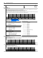
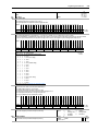
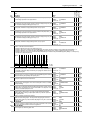
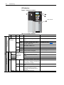
1
PowerFlex 700S
High Performance
AC Drive
User Manual
Important User Information
Solid state equipment has operational characteristics differing from those of
electromechanical equipment. “Safety Guidelines for the Application,
Installation and Maintenance of Solid State Controls” (Publication SGI-1.1
available from your local Allen-Bradley Sales Office or online at http://
www.ab.com/manuals/gi) describes some important differences between
solid state equipment and hard-wired electromechanical devices. Because of
this difference, and also because of the wide variety of uses for solid state
equipment, all persons responsible for applying this equipment must satisfy
themselves that each intended application of this equipment is acceptable.
In no event will the Allen-Bradley Company be responsible or liable for
indirect or consequential damages resulting from the use or application of
this equipment.
The examples and diagrams in this manual are included solely for
illustrative purposes. Because of the many variables and requirements
associated with any particular installation, the Allen-Bradley Company
cannot assume responsibility or liability for actual use based on the
examples and diagrams.
No patent liability is assumed by Allen-Bradley Company with respect to
use of information, circuits, equipment, or software described in this
manual.
Reproduction of the contents of this manual, in whole or in part, without
written permission of the Allen-Bradley Company is prohibited.
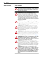
Throughout this manual we use notes to make you aware of safety
considerations.
!
ATTENTION: Identifies information about practices or
circumstances that can lead to personal injury or death, property
damage, or economic loss.
Attentions help you:
• identify a hazard
• avoid the hazard
• recognize the consequences
Important: Identifies information that is especially important for successful
application and understanding of the product.
Shock Hazard labels may be located on or inside the drive to
alert people that dangerous voltage may be present.
SCANport is a trademark of Rockwell Automation.
PLC is a registered trademark of Rockwell Automation.
COLOR-KEYED is a registered trademark of Thomas & Betts Corporation.
IBM is a registered trademark of International Business Machines Corporation.
Windows 95 is a registered trademark of Microsoft Corporation.
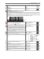
Summary of Changes
This information summarizes the changes to the PowerFlex 700S User
Manual, publication 20D-UM001 since the last release.
Manual Updates
Change
Catalog Number Explanation updated.
AC Input Phase Selection has been updated.
Selecting/Verifying Fan Voltage has been updated.
Cooling Fan Voltage added.
Power Terminal Block information for Frames 4 & 6 added.
Disconnecting MOVs and Common Mode Capacitors updated.
Typical Terminal Block Locations added
Power Terminal Blocks added - Frame 4 & 6 and Common Bus
I/O Wiring Diagrams updated.
PowerFlex 700S EN61800-3 EMC Compatibility
Programming and Parameters Chapter updated.
Over Frequency Fault - Fault 22 added.
Faults Cleared - Fault 65 added
Specifications Table updated.
Recommended Protection Devices Tables updated.
540 and 650V DC Input Recommended Protection Devices Tables added.
PowerFlex 700S Frames AC Input Table updated.
Frame 4 Dimensions added.
Frame 6 Dimensions added.
Frame 4 Bottom View Dimensions added.
Frame 6 Bottom View Dimensions added.
See Page...
Preface-5
1-9
1-9
1-9
1-10
1-15
1-11
1-12-1-13
1-21-1-30
1-35
3-1-3-98
4-7
4-5
A-1
A-9-A-11
A-12
A-15
A-17
A-19
A-22
A-24
soc-2
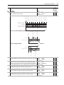
Table of Contents
i
Important User Information . . . . . . . . . . . . . . . . . . . . . . . . . . . . . . . . . . . . . . . . . . . . . . . 1-2
Summary of
Changes
Manual Updates . . . . . . . . . . . . . . . . . . . . . . . . . . . . . . . . . . . . . . . . . . . . . . . . . . . . . . . . . i-1
Preface
Overview
Who Should Use This Manual . . . . . . . . . . . . . . . . . . . . . . . . . . . . . . . . . . . . . . . . . . . . .
What Is Not In This Manual . . . . . . . . . . . . . . . . . . . . . . . . . . . . . . . . . . . . . . . . . . . . . . .
Recommended Documentation . . . . . . . . . . . . . . . . . . . . . . . . . . . . . . . . . . . . . . . . . . . . .
Manual Conventions . . . . . . . . . . . . . . . . . . . . . . . . . . . . . . . . . . . . . . . . . . . . . . . . . . . . .
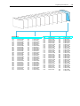
Drive Frame Sizes . . . . . . . . . . . . . . . . . . . . . . . . . . . . . . . . . . . . . . . . . . . . . . . . . . . . . . .
General Precautions . . . . . . . . . . . . . . . . . . . . . . . . . . . . . . . . . . . . . . . . . . . . . . . . . . . . .
Class 1 LED Product . . . . . . . . . . . . . . . . . . . . . . . . . . . . . . . . . . . . . . . . . . . . . . . . . . .
Catalog Number Explanation . . . . . . . . . . . . . . . . . . . . . . . . . . . . . . . . . . . . . . . . . . . . . .
P-1
P-1
P-1
P-3
P-3
P-4
P-4
P-5
ii
Chapter 1
Installation/Wiring
Chapter Objectives. . . . . . . . . . . . . . . . . . . . . . . . . . . . . . . . . . . . . . . . . . . . . . . . . . . . . . . 1-1
Opening the Cover . . . . . . . . . . . . . . . . . . . . . . . . . . . . . . . . . . . . . . . . . . . . . . . . . . . . . . . 1-2
Mounting Clearances . . . . . . . . . . . . . . . . . . . . . . . . . . . . . . . . . . . . . . . . . . . . . . . . . . . . . 1-2
Operating Temperatures. . . . . . . . . . . . . . . . . . . . . . . . . . . . . . . . . . . . . . . . . . . . . . . . . 1-3
AC Supply Source Considerations. . . . . . . . . . . . . . . . . . . . . . . . . . . . . . . . . . . . . . . . . . . 1-3
Unbalanced or Ungrounded Distribution Systems . . . . . . . . . . . . . . . . . . . . . . . . . . . . 1-3
Input Power Conditioning . . . . . . . . . . . . . . . . . . . . . . . . . . . . . . . . . . . . . . . . . . . . . . . 1-4
Grounding Requirements. . . . . . . . . . . . . . . . . . . . . . . . . . . . . . . . . . . . . . . . . . . . . . . . . . 1-4
Recommended Grounding Scheme . . . . . . . . . . . . . . . . . . . . . . . . . . . . . . . . . . . . . . . . 1-4
Shield Termination - SHLD . . . . . . . . . . . . . . . . . . . . . . . . . . . . . . . . . . . . . . . . . . . . . . 1-5
RFI Filter Grounding . . . . . . . . . . . . . . . . . . . . . . . . . . . . . . . . . . . . . . . . . . . . . . . . . . . 1-5
Fuses and Circuit Breakers . . . . . . . . . . . . . . . . . . . . . . . . . . . . . . . . . . . . . . . . . . . . . . . . 1-5
Power Wiring . . . . . . . . . . . . . . . . . . . . . . . . . . . . . . . . . . . . . . . . . . . . . . . . . . . . . . . . . . . 1-6
Power Cable Types Acceptable for 200-600 Volt Installations . . . . . . . . . . . . . . . . . . . 1-6
Motor Cable Lengths . . . . . . . . . . . . . . . . . . . . . . . . . . . . . . . . . . . . . . . . . . . . . . . . . . . 1-8
Power Terminal Block . . . . . . . . . . . . . . . . . . . . . . . . . . . . . . . . . . . . . . . . . . . . . . . . . . 1-8
Cable Entry Plate Removal . . . . . . . . . . . . . . . . . . . . . . . . . . . . . . . . . . . . . . . . . . . . . . 1-8
Access Panel Removal. . . . . . . . . . . . . . . . . . . . . . . . . . . . . . . . . . . . . . . . . . . . . . . . . . 1-8
Replace the cover when wiring is complete.
AC Input Phase Selection (Frames 5 & 6 Only) . . . . . . . . . . . . . . . . . . . . . . . . . . . . . . 1-8
Cooling Fan Voltage . . . . . . . . . . . . . . . . . . . . . . . . . . . . . . . . . . . . . . . . . . . . . . . . . . . 1-9
Selecting/Verifying Fan Voltage (Frames 5 & 6 Only) . . . . . . . . . . . . . . . . . . . . . . . . . 1-9
Dynamic Brake Resistor Considerations . . . . . . . . . . . . . . . . . . . . . . . . . . . . . . . . . . . 1-14
Using Input/Output Contactors . . . . . . . . . . . . . . . . . . . . . . . . . . . . . . . . . . . . . . . . . . . . 1-15
Disconnecting MOVs and Common Mode Capacitors . . . . . . . . . . . . . . . . . . . . . . . . . . 1-15
I/O Wiring . . . . . . . . . . . . . . . . . . . . . . . . . . . . . . . . . . . . . . . . . . . . . . . . . . . . . . . . . . . . 1-18
Wiring the Main Control Board I/O Terminals . . . . . . . . . . . . . . . . . . . . . . . . . . . . . . 1-19
Main Control Board I/O Configuration Settings . . . . . . . . . . . . . . . . . . . . . . . . . . . . . 1-31
Connecting SynchLink . . . . . . . . . . . . . . . . . . . . . . . . . . . . . . . . . . . . . . . . . . . . . . . . . . 1-32
Class 1 LED Product . . . . . . . . . . . . . . . . . . . . . . . . . . . . . . . . . . . . . . . . . . . . . . . . . . 1-32
EMC Instructions. . . . . . . . . . . . . . . . . . . . . . . . . . . . . . . . . . . . . . . . . . . . . . . . . . . . . . . 1-34
CE Conformity. . . . . . . . . . . . . . . . . . . . . . . . . . . . . . . . . . . . . . . . . . . . . . . . . . . . . . . 1-34
Low Voltage Directive (73/23/EEC) . . . . . . . . . . . . . . . . . . . . . . . . . . . . . . . . . . . . . . 1-34
EMC Directive (89/336/EEC) . . . . . . . . . . . . . . . . . . . . . . . . . . . . . . . . . . . . . . . . . . . 1-34
General Notes . . . . . . . . . . . . . . . . . . . . . . . . . . . . . . . . . . . . . . . . . . . . . . . . . . . . . . . 1-34
Essential Requirements for CE Compliance . . . . . . . . . . . . . . . . . . . . . . . . . . . . . . . . 1-35
Chapter 2
Start-Up
Prepare for Drive Start-Up. . . . . . . . . . . . . . . . . . . . . . . . . . . . . . . . . . . . . . . . . . . . . . . . .
Before Applying Power to the Drive . . . . . . . . . . . . . . . . . . . . . . . . . . . . . . . . . . . . . . .
Applying Power to the Drive . . . . . . . . . . . . . . . . . . . . . . . . . . . . . . . . . . . . . . . . . . . . .
Status Indicators. . . . . . . . . . . . . . . . . . . . . . . . . . . . . . . . . . . . . . . . . . . . . . . . . . . . . . . . .
Assisted Start-Up . . . . . . . . . . . . . . . . . . . . . . . . . . . . . . . . . . . . . . . . . . . . . . . . . . . . . . . .
Chapter 3
2-1
2-1
2-2
2-3
2-4
Programming and Parameters
About Parameters. . . . . . . . . . . . . . . . . . . . . . . . . . . . . . . . . . . . . . . . . . . . . . . . . . . . . . . . 3-1
How Parameters are Organized . . . . . . . . . . . . . . . . . . . . . . . . . . . . . . . . . . . . . . . . . . . . . 3-3
Parameter Data in Linear List Format . . . . . . . . . . . . . . . . . . . . . . . . . . . . . . . . . . . . . . . 3-16
Parameter Cross Reference By Name . . . . . . . . . . . . . . . . . . . . . . . . . . . . . . . . . . . . . . . 3-94
Table of Contents
Chapter 4
Troubleshooting
Chapter Objectives . . . . . . . . . . . . . . . . . . . . . . . . . . . . . . . . . . . . . . . . . . . . . . . . . . . . . .
Faults and Alarms . . . . . . . . . . . . . . . . . . . . . . . . . . . . . . . . . . . . . . . . . . . . . . . . . . . . . . .
Drive Status . . . . . . . . . . . . . . . . . . . . . . . . . . . . . . . . . . . . . . . . . . . . . . . . . . . . . . . . . . . .
LED Indications . . . . . . . . . . . . . . . . . . . . . . . . . . . . . . . . . . . . . . . . . . . . . . . . . . . . . .
HIM Indication . . . . . . . . . . . . . . . . . . . . . . . . . . . . . . . . . . . . . . . . . . . . . . . . . . . . . . .
Manually Clearing Faults . . . . . . . . . . . . . . . . . . . . . . . . . . . . . . . . . . . . . . . . . . . . . . . . .
Fault Descriptions . . . . . . . . . . . . . . . . . . . . . . . . . . . . . . . . . . . . . . . . . . . . . . . . . . . . . . .
Appendix A
iii
4-1
4-1
4-1
4-2
4-3
4-4
4-4
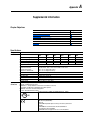
Supplemental Information
Chapter Objectives . . . . . . . . . . . . . . . . . . . . . . . . . . . . . . . . . . . . . . . . . . . . . . . . . . . . . . A-1
Specifications . . . . . . . . . . . . . . . . . . . . . . . . . . . . . . . . . . . . . . . . . . . . . . . . . . . . . . . . . . A-1
DPI Communication Configurations. . . . . . . . . . . . . . . . . . . . . . . . . . . . . . . . . . . . . . . . . A-5
Typical Programmable Controller Configurations . . . . . . . . . . . . . . . . . . . . . . . . . . . . A-5
Logic Command Word . . . . . . . . . . . . . . . . . . . . . . . . . . . . . . . . . . . . . . . . . . . . . . . . . A-5
Logic Status Word . . . . . . . . . . . . . . . . . . . . . . . . . . . . . . . . . . . . . . . . . . . . . . . . . . . . . A-6
Output Devices . . . . . . . . . . . . . . . . . . . . . . . . . . . . . . . . . . . . . . . . . . . . . . . . . . . . . . . . . A-6
Drive, Fuse & Circuit Breaker Ratings . . . . . . . . . . . . . . . . . . . . . . . . . . . . . . . . . . . . . . . A-6
Fuse Size . . . . . . . . . . . . . . . . . . . . . . . . . . . . . . . . . . . . . . . . . . . . . . . . . . . . . . . . . . . . A-6
Fuse Type . . . . . . . . . . . . . . . . . . . . . . . . . . . . . . . . . . . . . . . . . . . . . . . . . . . . . . . . . . . A-7
List of Motors with Compatible Thermistor Ratings . . . . . . . . . . . . . . . . . . . . . . . . . . . A-13
Spare Connectors . . . . . . . . . . . . . . . . . . . . . . . . . . . . . . . . . . . . . . . . . . . . . . . . . . . . . . A-14
Main Control Board . . . . . . . . . . . . . . . . . . . . . . . . . . . . . . . . . . . . . . . . . . . . . . . . . . A-14
High Resolution Encoder Interface Board . . . . . . . . . . . . . . . . . . . . . . . . . . . . . . . . . A-14
Resolver Interface Board. . . . . . . . . . . . . . . . . . . . . . . . . . . . . . . . . . . . . . . . . . . . . . . A-14
Dimensions . . . . . . . . . . . . . . . . . . . . . . . . . . . . . . . . . . . . . . . . . . . . . . . . . . . . . . . . . . . A-15
Frame 1 . . . . . . . . . . . . . . . . . . . . . . . . . . . . . . . . . . . . . . . . . . . . . . . . . . . . . . . . . . . . A-20
Frame 2 . . . . . . . . . . . . . . . . . . . . . . . . . . . . . . . . . . . . . . . . . . . . . . . . . . . . . . . . . . . . A-20
Frame 3 - All Drives except 50 HP, 480V (37 kW, 400V) . . . . . . . . . . . . . . . . . . . . . A-21
Frame 3 - 50 HP, 480V (37 kW, 400V) Normal Duty Drive . . . . . . . . . . . . . . . . . . . A-21
Frame 4 . . . . . . . . . . . . . . . . . . . . . . . . . . . . . . . . . . . . . . . . . . . . . . . . . . . . . . . . . . . . A-22
Frame 5 - 75 HP, 480V (55 kW, 400V) Normal Duty Drive . . . . . . . . . . . . . . . . . . . A-23
Frame 5 - 100 HP, 480V (55 kW, 400V) Normal Duty Drive . . . . . . . . . . . . . . . . . . A-23
Frame 6 . . . . . . . . . . . . . . . . . . . . . . . . . . . . . . . . . . . . . . . . . . . . . . . . . . . . . . . . . . . . A-24
Appendix B
Control Block Diagrams
Appendix C
Hi-Resolution Encoder Feedback Option
Chapter Objectives . . . . . . . . . . . . . . . . . . . . . . . . . . . . . . . . . . . . . . . . . . . . . . . . . . . . . .
Specifications . . . . . . . . . . . . . . . . . . . . . . . . . . . . . . . . . . . . . . . . . . . . . . . . . . . . . . . . . .
Hi-Resolution Feedback Option Card Specifications . . . . . . . . . . . . . . . . . . . . . . . . . .
Supported Encoders. . . . . . . . . . . . . . . . . . . . . . . . . . . . . . . . . . . . . . . . . . . . . . . . . . . .
Recommended Cables . . . . . . . . . . . . . . . . . . . . . . . . . . . . . . . . . . . . . . . . . . . . . . . . . .
Wiring the Hi-Resolution Feedback Option Card to an Encoder . . . . . . . . . . . . . . . . . . .
C-1
C-1
C-1
C-1
C-2
C-2
iv
Appendix D
HIM Overview
External and Internal Connections. . . . . . . . . . . . . . . . . . . . . . . . . . . . . . . . . . . . . . . . . . .
LCD Display Elements . . . . . . . . . . . . . . . . . . . . . . . . . . . . . . . . . . . . . . . . . . . . . . . . . . .
ALT Functions . . . . . . . . . . . . . . . . . . . . . . . . . . . . . . . . . . . . . . . . . . . . . . . . . . . . . . . . . .
Removing/Installing the HIM . . . . . . . . . . . . . . . . . . . . . . . . . . . . . . . . . . . . . . . . . . . . . .
Index
D-1
D-2
D-2
D-3
Preface
Overview
The purpose of this manual is to provide you with the basic information
needed to install, start-up and troubleshoot the PowerFlex 700S Adjustable
Frequency AC Drive.
For information on …
Who Should Use This Manual
What Is Not In This Manual
Recommended Documentation
Manual Conventions
Drive Frame Sizes
General Precautions
Catalog Number Explanation
See page...
Preface-1
Preface-1
Preface-1
Preface-3
Preface-3
Preface-4
Preface-5
Who Should Use This
Manual
This manual is intended for qualified personnel. You must be able to
program and operate Adjustable Frequency AC Drive devices. In addition,
you must have an understanding of the parameter settings and functions.
You must also understand programmable controllers for the PowerFlex
700S with DriveLogix.
What Is Not In This Manual
Since this User Manual is designed to provide only basic start-up
information, the following topic has not been included:
• Spare Parts Information
For detailed drive information, please refer to publication PowerFlex 700S
Reference Manual, Vol 2. This pubication is available online at:
www.theautomationbookstore.com
Recommended
Documentation
The following publications provide general drive information.
Title
Wiring and Grounding for PWM AC
Drives
Safety Guidelines for the
Application, Installation and
Maintenance of Solid State Control
A Global Reference Guide for
Reading Schematic Diagrams
Guarding Against Electrostatic
Damage
Publication
DRIVES-IN001
Available…
www.theautomationbookstore.com
SGI-1.1
www.ab.com/manuals/dr/
index3.html#Safety
0100-2.10
www.theautomationbookstore.com
8000-4.5.2
www.ab.com/manuals/dr/
index3.html#Safety
p-2
Overview
The following publications provide specific PowerFlex drive information.
Title
Installation Instructions Hi-Resolution Encoder Feedback
Option for PowerFlex 700S Drives
Installation Instructions - Resolver
Feedback Option for PowerFlex
700S Drives
Firmware Release Notes PowerFlex 700S Drive (firmware
revision 1.14)
Publication
20D-IN001
Available…
20D-IN002
www.ab.com/manuals/dr
20D-RN004
For detailed PowerFlex 700S information:
Title
Publication
PowerFlex Reference Manual, Vol. 2 PFLEX-RM001
Available…
On CD supplied with drive or
www.ab.com/manuals/dr
The following publications provide necessary information when applying
the DriveLogix Controller.
Title
Publication
DriveLogix Controller User Manual 20D-UM002
Firmware Release Notes DriveLogix Controller (firmware
revsion 10.15)
Firmware Release Notes DriveLogix Controller (firmware
revsion 10.16)
Firmware Release Notes DriveLogix Controller (firmware
revsion 11.14)
Logix5000 Controllers Common
Procedures
Installation Instructions DriveLogix Controller for
PowerFlex 700S Drives
Logix5000 Controllers General
Instructions
ControlNet Daughtercard
Installation Instructions
ControlNet Daughtercard
Installation Instructions
Logix5000 Controllers Process
Control and Drives Instructions
RSLogix 5000 Getting Results
RSNetworx for ControlNet Getting
Results
RSLinx Getting Results Guide
20D-RN001
Available…
On CD supplied with drive or
www.ab.com/manuals/dr
www.ab.com/manuals/dr
20D-RN002
www.ab.com/manuals/dr
20D-RN003
www.ab.com/manuals/dr
1756-PM001
www.ab.com/manuals/fl/
20D-IN003
www.ab.com/manuals/dr
1756-RM003
www.ab.com/manuals/fl/
1788-IN002
www.ab.com/manuals/cn
1788-IN005
www.ab.com/manuals/cn
1756-RM006
www.ab.com/manuals/fl/
9399-RLD300GR
9398-CNETGR
www.ab.com/manuals/swrsi/
www.ab.com/manuals/swrsi/
9399-LINXGR
www.ab.com/manuals/swrsi/
Overview
p-3
The following publications provide information that is useful when
planning and installing communication networks.
Title
ContolNet Coax Tap Installation
Instructions
ControlNet Cable System Planning
and Installation Manual
ContolNet Fiber Media Planning
and Installation Guide
SynchLink Design Guide
Manual Conventions
Publication
1786-5.7
Available…
www.ab.com/manuals/cn/controlnet.html
1786-6.2.1
www.ab.com/manuals/cn/controlnet.html
CNET-IN001
www.ab.com/manuals/cn/controlnet.html
1756-TD008
www.ab.com/manuals/cn/
• In this manual we refer to the PowerFlex 700S Adjustable Frequency AC
Drive as: drive, PowerFlex 700S or PowerFlex 700S Drive.
• To help differentiate parameter names and LCD display text from other
text, the following conventions will be used:
– Parameter Names will appear in [brackets] after the Parameter
Number.
For example: Parameter 307 [Output Voltage].
– Display text will appear in “quotes.” For example: “Enabled.”
• The following words are used throughout the manual to describe an
action:
Word
Can
Cannot
May
Must
Shall
Should
Should Not
Drive Frame Sizes
Meaning
Possible, able to do something
Not possible, not able to do something
Permitted, allowed
Unavoidable, you must do this
Required and necessary
Recommended
Not recommended
Similar PowerFlex 700S drive sizes are grouped into frame sizes to simplify
spare parts ordering, dimensioning, etc. A cross reference of drive catalog
numbers and their respective frame size is provided in Appendix A.
p-4
Overview
General Precautions
Class 1 LED Product
!
!
!
!
!
!
!
!
ATTENTION: Hazard of permanent eye damage exists when
using optical transmission equipment. This product emits intense
light and invisible radiation. Do not look into module ports or
fiber optic cable connectors.
ATTENTION: This drive contains ESD (Electrostatic
Discharge) sensitive parts and assemblies. Static control
precautions are required when installing, testing, servicing or
repairing this assembly. Component damage may result if ESD
control procedures are not followed. If you are not familiar with
static control procedures, reference A-B publication 8000-4.5.2,
“Guarding Against Electrostatic Damage” or any other applicable
ESD protection handbook.
ATTENTION: An incorrectly applied or installed drive can
result in component damage or a reduction in product life. Wiring
or application errors, such as, undersizing the motor, incorrect or
inadequate AC supply, or excessive ambient temperatures may
result in malfunction of the system.
ATTENTION: Only qualified personnel familiar with the
PowerFlex 700S Drive and associated machinery should plan or
implement the installation, start-up and subsequent maintenance
of the system. Failure to comply may result in personal injury
and/or equipment damage.
ATTENTION: To avoid an electric shock hazard, verify that the
voltage on the bus capacitors has discharged before performing
any work on the drive. Measure the DC bus voltage at the +DC &
–DC terminals of the Power Terminal Block (refer to Chapter 1
for location). The voltage must be zero.
ATTENTION: Risk of injury or equipment damage exists. DPI
or SCANport host products must not be directly connected
together via 1202 cables. Unpredictable behavior can result if two
or more devices are connected in this manner.
ATTENTION: Risk of injury or equipment damage exists.
Parameters 365 [Encdr0 Loss Cnfg] - 394 [VoltFdbkLossCnfg] let
you determine the action of the drive in response to operating
anomalies. Precautions should be taken to ensure that the settings
of these parameters do not create hazards of injury or equipment
damage.
ATTENTION: Risk of injury or equipment damage exists.
Parameters 383 [SL CommLoss Data] - 392 [NetLoss DPI Cnfg]
let you determine the action of the drive if communications are
disrupted. You can set these parameters so that the drive continues
to run. Precautions should be taken to ensure that the settings of
these parameters do not create hazards of injury or equipment
damage.
Overview
p-5
Catalog Number
Explanation
Position
11
1-3
4
5-7
8
9
10
12
13
14
15
16
17
20D
D
2P1
A
0
E
Y
N
A
N
N
N
N
Drive
Voltage Rating
Rating
Enclosure
HIM
Documentation
Brake
Brake
Resistor
Emission
Comm Slot
I/O
Feedback
Additional
Config
Code Type
20D PowerFlex
700S
Code
B
C
D
H
J
P
R
Voltage
240V AC
400V AC
480V AC
540V DC
650V DC
540V DC
650V DC
Code w/Resistor
Y
Yes
N
No
Ph.
3
3
3
—
—
—
—
DC Precharge
—
—
—
N
N
Y
Y
Code
0
2
3
4
5
Operator Interface
Blank Cover
Digital LCD
Full Numeric LCD
Analog LCD
Prog. Only LCD
Code Enclosure
A
IP 20, NEMA Type 1
Code Rating
A
Filtered
Output Current @ 480V 60Hz Input
Code
Amps
HP
1P1
1.1
0.5
2P1
2.1
1.0
3P4
3.4
2.0
5P0
5
3.0
8P0
8
5.0
011
11
7.5
014
14
10
022
22
15
027
27
20
034
34
25
040
40
30
052
52
40
065
65
50
096
96
75
125
125
100
156
156
125
180
180
150
Code
N
A
B
Option
None
Resolver
Hi-Resolution Stegman Encoder
Code
N
A
B
Code w/Brake IGBT
Y
Yes
N
No
Code Documents
E
Quick Start Guide and CD
N
No Documentation
Output Current @ 230V 60Hz Input
Code
Amps
HP
2P2
2.2
0.5
4P2
4.2
1.0
6P8
6.8
2.0
9P6
9.6
3.0
015
15.3
5.0
022
22
7.5
028
28
10
042
42
15
052
52
20
Code Type Voltage
N
None N/A
Code
C
D
R
S
E
1
2
3
4
5
6
N
Logix Options
None
DriveLogix5720
DriveLogix 5720 w/
Expanded Memory
Version
DPI ControlNet (Coax)
DPI DeviceNet
DPI RIO
DPI RS-483 DF1 ➌
DPI EtherNet/IP ➌
DriveLogix ControlNet (Coax)
DriveLogix ControlNet Redundant (Coax)
DriveLogix ControlNet (Fiber)
DriveLogix ControlNet Redundant (Fiber)
DriveLogix DeviceNet (Open Conn.)
DriveLogix EtherNet/IP (Twisted Pair)
None
Important: This table is not indended for ordering. For a full list of current
options refer to publication 20D-PL001, PowerFlex 700S/700S
DriveLogix USA Price List.
p-6
Notes:
Overview
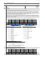
Chapter
1
Installation/Wiring
Chapter Objectives
This chapter provides the information needed to mount and wire the
PowerFlex 700S AC drive.
For Information on …
Opening the Cover
Mounting Clearances
AC Supply Source Considerations
Grounding Requirements
Fuses and Circuit Breakers
Power Wiring
Using Input/Output Contactors
Disconnecting MOVs and Common Mode Capacitors
I/O Wiring
Connecting SynchLink
EMC Instructions
See Page...
1-2
1-2
1-3
1-4
1-5
1-6
1-16
1-16
1-19
1-33
1-35
Since most start-up difficulties are the result of incorrect wiring, take every
precaution to assure the wiring is correct. Read and understand all items in
this chapter before beginning installation.
!
ATTENTION: The following information is merely a guide for
proper installation. The Allen-Bradley Company cannot assume
responsibility for the compliance or the noncompliance to any
code, national, local or otherwise for the proper installation of this
drive or associated equipment. A hazard of personal injury and/or
equipment damage exists if codes are ignored during installation.
1-2
Installation/Wiring
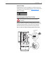
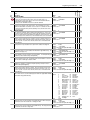
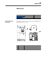
Opening the Cover
B
DRIVE
DRIVE
ENABLE
SYNCHLINK
A
B
C
Auto / Man
8
9
4
5
1
2
3
.
0
+/-
Exit
Esc
Sel
Opening Control Assembly
Step
Lang
7
S.M.A.R.T.
Alt
Description
Loosen captive screw.
Push down on cover.
Pull cover away from assembly.
Exp
6
Remove
Jog
Param #
Opening Power Structure
Pull up on locking tab and swing door
open.
Special hinges allow the cover to move
away from drive and lay on top of
adjacent drive (if present).
C
A
Mounting Clearances
101.6mm
No
(4.0 in.)
Adhesive Label
(see below)
With Adhesive Label
50.8mm (2.0 in)
101.6mm
(4.0 in.)
50.8mm (2.0 in)
101.6mm
(4.0 in.)
(see below)
101.6mm
(4.0 in.)
Refer to the PowerFlex Reference
Manual Vol. 2 for detailed
dimension information
Installation/Wiring
1-3
Operating Temperatures
PowerFlex 700S drives are designed to operate in surrounding air
temperature of 0° to 40° C. To operate the drive in installations with
surrounding air temperature between 41° and 50° C, remove the adhesive
label affixed to the top of the drive enclosure.
Important: Removing the adhesive label from the drive changes the NEMA
enclosure rating from Type 1 to Open type.
AC Supply Source
Considerations
PowerFlex drives are suitable for use on a circuit capable of delivering up to
a maximum of 200,000 rms symmetrical amperes, 600 volts with
recommended fuses/circuit breakers. Refer to the PowerFlex Reference
Manual Vol. 2 for actual interrupt ratings based on circuit breaker or fuse
choice.
!
ATTENTION: To guard against personal injury and/or
equipment damage caused by improper fusing or circuit breaker
selection, use only the recommended line fuses/circuit breakers
specified in Appendix A.
If a Residual Current Detector (RCD) is used as a system ground fault
monitor, only Type B (adjustable) devices should be used to avoid nuisance
tripping.
Unbalanced or Ungrounded Distribution Systems
If phase to ground voltage will exceed 125% of normal or the supply system
is ungrounded, refer to the PowerFlex Reference Manual Vol. 2 for more
information.
!
ATTENTION: PowerFlex 700S drives contain protective MOVs
and common mode capacitors that are referenced to ground.
These devices should be disconnected if the drive is installed on
an ungrounded distribution system. See page page 1-18 for
jumper locations.
1-4
Installation/Wiring
Input Power Conditioning
Certain events on the power system supplying a drive can cause component
damage or shortened product life. These conditions are divided into 2 basic
categories:
1. All Drives
– The power system has power factor correction capacitors switched in
and out of the system, either by the user or by the power company.
– The power source has intermittent voltage spikes in excess of 6000
volts. These spikes could be caused by other equipment on the line or
by events such as lightning strikes.
– The power source has frequent interruptions.
2. 5 HP or Less Drives (in addition to “1” above)
– The nearest supply transformer is larger than 100kVA or the available
short circuit (fault) current is greater than 100,000A.
– The impedance in front of the drive is less than 0.5%.
If any or all of these conditions exist, it is recommended that the user install
a minimum amount of impedance between the drive and the source. This
impedance could come from the supply transformer itself, the cable
between the transformer and drive or an additional transformer or reactor.
The impedance can be calculated using the information supplied in either
the PowerFlex Reference Manual Vol. 2 or the technical document Wiring
and Grounding Guidelines, publication DRIVES-IN001.
Grounding Requirements
The drive Safety Ground-PE must be connected to system ground.
Ground impedance must conform to the requirements of national and local
industrial safety regulations and/or electrical codes. The integrity of all
ground connections should be periodically checked.
Recommended Grounding Scheme
A single point (PE only) grounding scheme should be used. Some
applications may require alternate grounding schemes, refer to the Wiring
and Grounding Guidelines for PWM AC Drives, publication number
DRIVES-IN001 for more information. These applications include
installations with long distances between drives or drive line-ups, which
could cause large potential differences between the drive or line-up grounds.
For installations within a cabinet, a single safety ground point or ground bus
bar connected directly to building steel should be used. All circuits
including the AC input ground conductor should be grounded
independently and directly to this point/bar.
Installation/Wiring
1-5
Figure 1.1 Typical Grounding
R
(L1)
S
(L2)
T
(L3)
PE
U
(T1)
V
(T2)
W
(T3)
DC
+
DC
–
BR1
BR2
Required
Input Fusing
Required Branch
Circuit Disconnect
Shield Termination - SHLD
The Shield terminal (see Figure 1.3 on page 1-11) provides a grounding
point for the motor cable shield. It must be connected to an earth ground by
a separate continuous lead. The motor cable shield should be connected to
this terminal on the drive (drive end) and the motor frame (motor end). Use
a shield terminating or EMI clamp to connect shield to this terminal.
RFI Filter Grounding
Using an optional RFI filter may result in relatively high ground leakage
currents. Therefore, the filter must only be used in installations with
grounded AC supply systems and be permanently installed and solidly
grounded (bonded) to the building power distribution ground. Ensure that
the incoming supply neutral is solidly connected (bonded) to the same
building power distribution ground. Grounding must not rely on flexible
cables and should not include any form of plug or socket that would permit
inadvertent disconnection. Some local codes may require redundant ground
connections. The integrity of all connections should be periodically
checked. Refer to the instructions supplied with the filter.
Fuses and Circuit Breakers
The PowerFlex 700S can be installed with either input fuses or an input
circuit breaker. Local/national electrical codes may determine additional
requirements for these installations. Refer to Appendix A for recommended
fuses/circuit breakers.
!
ATTENTION: The PowerFlex 700S does not provide input
power short circuit protection. Specifications for the
recommended fuse or circuit breaker to provide drive input power
protection against short circuits are provided in Appendix A.
1-6
Installation/Wiring
Power Wiring
Power Cable Types Acceptable for 200-600 Volt Installations
!
ATTENTION: National Codes and standards (NEC, VDE, BSI
etc.) and local codes outline provisions for safely installing
electrical equipment. Installation must comply with specifications
regarding wire types, conductor sizes, branch circuit protection
and disconnect devices. Failure to do so may result in personal
injury and/or equipment damage.
A variety of cable types are acceptable for drive installations. For many
installations, unshielded cable is adequate, provided it can be separated
from sensitive circuits. As an approximate guide, allow a spacing of 0.3
meters (1 foot) for every 10 meters (32.8 feet) of length. In all cases, long
parallel runs must be avoided. Do not use cable with an insulation thickness
less than or equal to 15 mils (0.4 mm/0.015 in.). See Table 1.A.
Unshielded
THHN, THWN or similar wire is acceptable for drive installation in dry
environments provided adequate free air space and/or conduit fill rates
limits are provided. Do not use THHN or similarly coated wire in wet
areas. Any wire chosen must have a minimum insulation thickness of 15
Mils and should not have large variations in insulation concentricity.
Shielded/Armored Cable
Shielded cable contains all of the general benefits of multi-conductor cable
with the added benefit of a copper braided shield that can contain much of
the noise generated by a typical AC Drive. Strong consideration for shielded
cable should be given in installations with sensitive equipment such as
weigh scales, capacitive proximity switches and other devices that may be
affected by electrical noise in the distribution system. Applications with
large numbers of drives in a similar location, imposed EMC regulations or a
high degree of communications/networking are also good candidates for
shielded cable.
Shielded cable may also help reduce shaft voltage and induced bearing
currents for some applications. In addition, the increased impedance of
shielded cable may help extend the distance the motor can be located from
the drive without the addition of motor protective devices such as terminator
networks. Refer to Reflected Wave in Wiring and Grounding Guidelines for
PWM AC Drives, publication DRIVES-IN001.
Consideration should be given to all of the general specifications dictated by
the environment of the installation, including temperature, flexibility,
moisture characteristics and chemical resistance. In addition, a braided
shield should be included and specified by the cable manufacturer as having
coverage of at least 75%. An additional foil shield can be greatly improve
noise containment.
Installation/Wiring
1-7
A good example of recommended cable is Belden® 295xx (xx determines
gauge). This cable has 4 XLPE insulated conductors with a 100% coverage
foil and an 85% coverage copper braided shield (with drain wire)
surrounded by a PVC jacket.
Other types of shielded cable are available, but the selection of these types
may limit the allowable cable length. Particularly, some of the newer cables
twist 4 conductors of THHN wire and wrap them tightly with a foil shield.
This construction can greatly increase the cable charging current required
and reduce the overall drive performance. Unless specified in the individual
distance tables as tested with the drive, these cables are not recommended
and their performance against the lead length limits supplied is not known.
Table 1.A Recommended Shielded Wire
Location
Rating/Type
Description
Standard
(Option 1)
600V, 90° C (194° F)
XHHW2/RHW-2
Anixter
B209500-B209507,
Belden 29501-29507,
or equivalent
Four tinned copper conductors with XLPE insulation.
Copper braid/aluminum foil combination shield and tinned
copper drain wire.
PVC jacket.
Standard
(Option 2)
Tray rated 600V, 90°
C (194° F) RHH/
RHW-2
Anixter OLF-7xxxxx or
equivalent
Three tinned copper conductors with XLPE insulation.
5 mil single helical copper tape (25% overlap min.) with three
bare copper grounds in contact with shield.
PVC jacket.
Class I & II; Tray rated 600V, 90°
Division I & II C (194° F) RHH/
RHW-2
Anixter 7V-7xxxx-3G
or equivalent
Three bare copper conductors with XLPE insulation and
impervious corrugated continuously welded aluminum armor.
Black sunlight resistant PVC jacket overall.
Three copper grounds on #10 AWG and smaller.
EMC Compliance
Refer to EMC Instructions on page 1-35 for details.
Cable Trays and Conduit
If cable trays or large conduits are to be used, refer to guidelines presented
in the PowerFlex Reference Manual Vol. 2.
!
ATTENTION: To avoid a possible shock hazard caused by
induced voltages, unused wires in the conduit must be grounded
at both ends. For the same reason, if a drive sharing a conduit is
being serviced or installed, all drives using this conduit should be
disabled. This will help minimize the possible shock hazard from
“cross coupled” motor leads.
1-8
Installation/Wiring
Motor Cable Lengths
Typically, motor lead lengths less than 30 meters (100 feet) are acceptable.
Motor lead lengths of 30 meters (100 feet) to 246 meters (800 feet) require
shielded cable. If your application dictates longer lengths, refer to
publication 20D-TD001, Technical Data - PowerFlex 700S Drives, for
details.
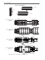
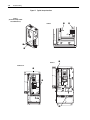
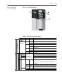
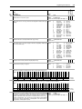
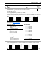
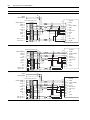
Power Terminal Block
Figure 1.3 shows the typical location of the Power Terminal Block in Frame
1 drives. The terminal block is located in the bottom section of the drive on
Frame 2-5 drives.
Cable Entry Plate Removal
If additional wiring access is needed, the Cable Entry Plate on Frame 1-3
drives can be removed. Simply loosen the screws securing the plate to the
chassis. The slotted mounting holes assure easy removal.
Important: Removing the Cable Entry Plate limits the maximum
surrounding air temperature to 40o C (104o F).
Access Panel Removal
Frame 3 drives utilize a panel/cover over the power wiring terminals. To
remove, simply slide it down and out.
Replace the cover when wiring is complete.
!
ATTENTION: Removing the access panel/cover exposes
dangerous voltages on the terminals and negates the enclosure
type rating. Replace the access panel/cover when service is
complete. Failure to comply may result in personal injury or
equipment damage.
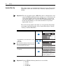
AC Input Phase Selection (Frames 5 & 6 Only)
!
ATTENTION: To avoid a shock hazard, ensure that all
power to the drive has been removed before performing
the following.
Moving the “Line Type” jumper shown in Figure 1.2 will select single or
three-phase operation. Remove plastic guard to access jumper.
Important: When selecting single-phase operation, input power must be
applied to the R (L1) and S (L2) terminals only.
Installation/Wiring
1-9
Cooling Fan Voltage
Common Bus drives require user supplied 120 or 240V AC to power the
cooling fans. Power source is connected between “0 VAC” and the terminal
corresponding to your source voltage (see Figure 1.5 on page 1-13).
Table 1.B Fan VA Rating
Frame
5
6
Fan Voltage(120V or 240V)
100 VA
138 VA
Selecting/Verifying Fan Voltage (Frames 5 & 6 Only)
!
ATTENTION: To avoid a shock hazard, ensure that all
power to the drive has been removed before performing
the following.
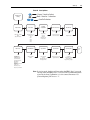
Frames 5 & 6 utilize a transformer to match the input line voltage to the
internal fan voltage. If your line voltage is different than the voltage class
specified on the drive nameplate, it may be necessary to change the
transformer taps. The taps are shown in the insert of frame 5 below.
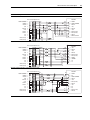
Figure 1.2 Frames 5 & 6 Jumper and Transformer Locations (Frame 5 shown)
Sin
gle
-Ph
as
Th
e
ree
(de -Ph
fau ase
lt)
Phase Selection
Jumper
Line Type
Spare
Optional
Communications
Module
Spare
Fan Voltage
300 VDC EXT PWR SPLY TERM (PS+, PS-)
POWER TERMINAL RATINGS
WIRE RANGE: 14-1/0 AWG (2.5-35 MM2)
TORQUE: 32 IN-LB (3.6 N-M)
STRIP LENGTH: 0.67 IN (17 MM)
USE 75 C CU WIRE ONLY
WIRE RANGE: 22-10 AWG (0.5-4 MM2)
TORQUE: 5.3 IN-LB (0.6 N-M)
STRIP LENGTH: 0.35 IN (9 MM)
9
17
GROUND TERMINAL RATINGS (PE)
WIRE RANGE: 6-1/0 AWG (16-35 MM2)
TORQUE: 44 IN-LB (5 N-M)
STRIP LENGTH: 0.83 IN (21 MM)
21
OUTPUT
INPUT AC
690 Volt Tap
600 Volt Tap
480 Volt Tap
400 Volt Tap
1-10
Installation/Wiring
Frame 6 Transformer Tap Access
The transformer is located behind the Power Terminal Block in the area
shown in Figure 1.2. Gain access by releasing the terminal block from the
rail. To release terminal block and change tap:
1. Locate the small metal tab at the bottom of the end block.
2. Press the tab in and pull the top of the block out. Repeat for next block if
desired.
3. Select appropriate transformer tap.
4. Replace block(s) in reverse order.
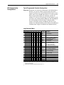
Table 1.C Power Terminal Block Specifications
No.
➊
Name
Power Terminal Block
Frame
1
2
3
4
5
(75 HP)(2)
5
(100 HP)(2)
6
Wire Size Range(1)
Torque
Maximum
Minimum
Maximum
Recommended
4.0 mm2
(10 AWG)
All power terminals
10.0 mm2
(6 AWG)
All power terminals
25.0 mm2
(3 AWG)
All power terminals
10.0 mm2
(6 AWG)
All power terminals
35.0 mm2
(1/0 AWG)
R, S, T, BR1, 2, DC+, DC-, 35.0 mm2
(1/0 AWG)
U, V and W
PE
35.0 mm2
(1/0 AWG)
R, S, T, DC+, DC-, U, V and 70.0 mm2
W
(3/0 AWG)
BR1, 2
35.0 mm2
(1/0 AWG)
PE
35.0 mm2
(1/0 AWG)
All power terminals
70.0 mm2
(250 MCM)
0.5 mm2
(22 AWG)
0.8 mm2
(18 AWG)
2.5 mm2
(14 AWG)
0.8 mm2
(18 AWG)
10 mm2
(8 AWG)
2.5 mm2
(14 AWG)
16.0 mm2
(6 AWG)
16.0 mm2
(4 AWG)
2.5 mm2
(14 AWG)
16.0 mm2
(6 AWG)
2.5 mm2
(14 AWG)
1.7 N-m
(15 lb.-in.)
1.7 N-m
(15 lb.-in.)
3.6 N-m
(32 lb.-in.)
1.7 N-m
(15 lb.-in.)
4.0 N-m
(24 lb.-in.)
3.6 N-m
(32 lb.-in.)
5 N-m
(44 lb.-in.)
15 N-m
(133 lb.-in.)
3.6 N-m
(32 lb.-in.)
5 N-m
(44 lb.-in.)
6 N-m
(52 lb.-in.)
0.8 N-m
(7 lb.-in.)
1.4 N-m
(12 lb.-in.)
1.8 N-m
(16 lb.-in.)
1.4 N-m
(12 lb.-in.)
4.0 N-m
(24 lb.-in.)
3.6 N-m
(32 lb.-in.)
5 N-m
(44 lb.-in.)
15 N-m
(133 lb.-in.)
3.6 N-m
(32 lb.-in.)
5 N-m
(44 lb.-in.)
6 N-m
(52 lb.-in.)
Description
All power terminals
➋
SHLD Terminal
1-6
Terminating point for wiring —
shields
—
1.6 N-m
(14 lb.-in.)
1.6 N-m
(14 lb.-in.)
➌
AUX Terminal Block
1-4
Auxiliary Control Voltage (3) 1.3 mm2
PS+, PS(16 AWG)
4.0 mm2
(10 AWG)
User Supplied Fan Voltage 4.0 mm2
0V AC, 120V AC, 240V AC (10 AWG)
0.2 mm2
(24 AWG)
0.5 mm2
(22 AWG)
0.5 mm2
(22 AWG)
—
—
0.6 N-m
(5.3 lb.-in.)
0.6 N-m
(5.3 lb.-in.)
0.6 N-m
(5.3 lb.-in.)
0.6 N-m
(5.3 lb.-in.)
5-6
➍
(1)
(2)
(3)
Fan Terminal Block
(Common Bus Only)
5-6
Maximum/minimum sizes that the terminal block will accept - these are not recommendations.
Not all terminals present on all drives.
External control power:
UL Installation - 300V DC, ±10%, Non UL Installation - 270-600V DC, ±10%.
Frame 1-6, 100 W
Installation/Wiring
Figure 1.3 Typical Power Terminal Block Location
Frame 2
Frame 1
Frame 3 & 4
➌
!
Optional
Communications
Module
DANGER
Optional
Communications
Module
Use 75C Wire Only
PE B
BR1
WIRE
STRIP
PE
BR1 B
➌
U/T1
V/T2
W/T3
R/L1
S/L2
V/T2 W/T3
PE A
PE R/L1 S/L2 T/L3
➌
AUX IN+ AUX OUT–
T/L3
SHLD
WIRE
STRIP
BR1 BR2
75C Cu Wire
6 AWG [10MM2] Max.
75C Cu Wire
3 AWG [25MM2] Max.
16 IN. LBS.
1.8 N-M } TORQUE
12 IN. LBS.
1.4 N-M } TORQUE
AUX IN
+ –
POWER
75C Cu Wire
2
6 AWG [10MM ] Max.
12 IN. LBS.
1.4 N-M } TORQUE
DC–
CONTROL
DC+
POWER
BR2
CONTROL
➊
#10-#14 AWG
Torque to 7 in-lbs
BR1 BR2 DC+ DC- U/T1 V/T2 W/T3 R/L1 S/L2 T/L3
SHLD
➊
PE
SHLD
/
SHLD
➋
➊
➋
➋
Frame 6
Frame 5
➋
➋
Optional
Communications
Module
Optional
Communications
Module
➌
➍
0 120 240
VAC VAC VAC
WIRE RANGE: 22-10 AWG (0.5-4 MM2)
TORQUE: 5.3 IN-LB (0.6 N-M)
STRIP LENGTH: 0.35 IN (9 MM)
➍
9
17
WIRE RANGE: 6-1/0 AWG (16-35 MM2)
TORQUE: 44 IN-LB (5 N-M)
STRIP LENGTH: 0.83 IN (21 MM)
21
INPUT AC
PS+
PS–
OUTPUT
WIRE STRIP
➌
300 VDC EXT PWR SPLY TERM (PS+, PS-)
POWER TERMINAL RATINGS
WIRE RANGE: 14-1/0 AWG (2.5-35 MM2)
TORQUE: 32 IN-LB (3.6 N-M)
STRIP LENGTH: 0.67 IN (17 MM)
USE 75 C CU WIRE ONLY
GROUND TERMINAL RATINGS (PE)
22-10
AWG
5.3 IN-LB
(0.6 N-M)
BR2
BR1
DC+
DC–
USE 75 C COPPER WIRE ONLY, TORQUE 52 IN-LB (6 N-M)
➊
Fan Terminal
Block
➊
USE 75 C
COPPER WIRE
ONLY
TORQUE
52 IN-LB
(6 N-M)
T1
T2
OUTPUT
T3
L1
L2
INPUT
L3
PE
1-11
1-12
Installation/Wiring
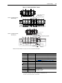
Figure 1.4 Power Terminal Block
BR1
BR2
DC+
DC–
PE
Frame 2
Frame 1
BR1 BR2 DC+ DC– PE
U (T1)
V (T2)
W (T3)
R (L1)
S (L2)
T (L3)
U V W R S T
(T1) (T2) (T3) (L1) (L2) (L3)
Frame 3
BR1 BR2 DC+ DC– U V W R S
T
(T1) (T2) (T3) (L1) (L2) (L3)
PS–
BR1/
BR2 DC+ DC+ DC– U/T1 V/T2 W/T3
PE
PE
R/L1 S/L2 T/L3
Frame 5 - 75 HP, Normal Duty
480V AC Input
PS+
BR2
BR1/
DC+
DC+
DC–
U/T1
V/T2
R/L1
W/T3
PE
PE
PS–
Frame 5 - 100 HP, Normal Duty
480V AC Input
PS+
PS–
BR1*/
BR2* DC+ DC+ DC–
U/T1 V/T2 W/T3
0 240
VAC VAC
PE
PE
Frame 5 - 75 HP, Normal Duty
650V DC Input
120
VAC
PS+
Precharge Resistor Fuse – FWP-15A14F
(Common Bus Drives w/Precharge Only)
PS–
BR1*/
BR2* DC+
DC+
DC–
U/T1
V/T2
W/T3
0 240
PEVAC VAC
PE
Frame 5 - 100 HP, Normal Duty
650V DC Input
PS+
120
VAC
Precharge Resistor Fuse – FWP-15A14F
(Common Bus Drives w/Precharge Only)
Shaded terminals (BR1 & BR2) will only be present on drives ordered with the Brake Option.
S/L2
T/L3
Installation/Wiring
PS+
PS–
WIRE STRIP
Figure 1.5 Power Terminal Block - Frame 6
22-10
AWG
5.3 IN-LB
(0.6 N-M)
BR2
BR1
DC+
Common Mode Capacitor
& MOV Jumpers
DC–
USE 75°C COPPER WIRE ONLY, TORQUE 52 IN-LB (6 N-M)
Input Filter Capacitor
Frame 6 - 150 HP, Normal Duty
480 V AC Input
USE 75°C
COPPER WIRE
ONLY
TORQUE
52 IN-LB
(6 N-M)
U
T1
V
T2
W
T3
PE
PE
R
L1
S
L2
Frame 6 - 150 HP, Normal Duty
650V DC Input
INPUT
Common Mode Capacitor
PS+
PS–
WIRE STRIP
OUTPUT
T
L3
& MOV Jumpers
22-10
AWG
5.3 IN-LB
(0.6 N-M)
BR2
BR1
DC+
DC–
Input Filter Capacitor
USE 75 C COPPER WIRE ONLY, TORQUE 52 IN-LB (6 N-M)
U
T1
V
T2
W
T3
PE
PE
22-10 AWG
5.3 IN-LB
(0.6 N-M)
OUTPUT
0 VAC
1-PHASE
TORQUE
52 IN-LB
(6 N-M)
FAN
INPUT
USE 75 C
COPPER WIRE
ONLY
0 VAC
120 VAC
240 VAC
Precharge Resistor Fuse – FWP-15A14F
(Common Bus Drives w/Precharge Only)
120V AC
240V AC
Shaded terminals (BR1 & BR2) will only be present on drives ordered with the Brake Option.
Terminal
BR1
BR2
DC+
DC–
PE
PS+
PSU
V
W
R
S
T
(1)
Description
DC Brake (+)
DC Brake (–)
DC Bus (+)
DC Bus (–)
PE Ground
Aux +
Aux Motor Ground
U (T1)
V (T2)
W (T3)
R (L1)
S (L2)
T (L3)
Notes
Dynamic Brake Resistor Connection (+)
Dynamic Brake Resistor Connection (–)
DC Input Power or Dynamic Brake Chopper
DC Input Power or Dynamic Brake Chopper
Refer to Figure 1.4 for location on 3 Frame drives
Auxiliary Control Voltage. See Table 1.C on page 1-10(1)
Auxiliary Control Voltage. See Table 1.C on page 1-10(1)
Refer to Figure 1.3 for location on 3 Frame drives
To motor
To motor
To motor
AC Line Input Power
Three-Phase = R, S & T
Single-Phase = R & S
External control power:
UL Installation - 300V DC, ±10%, Non UL Installation - 270-600V DC, ±10%.
1-3 Frame - 40 W, 165 mA, 5 Frame - 80 W, 90 mA
1-13
1-14
Installation/Wiring
Important Common Bus (DC Input) Application Notes
1. If drives without internal precharge are used (Frames 5 & 6 only), then:
a) precharge capability must be provided in the system to guard against
possible damage, and
b) disconnect switches Must Not be used between the input of the drive
and a common DC bus without the use of an external precharge
device.
2. If drives with internal precharge (Frames 0-6) are used with a disconnect
switch to the common bus, then:
a) an auxiliary contact on the disconnect must be connected to a digital
input of the drive. The corresponding input (parameter 361-366) must
be set to option 30, “Precharge Enable.” This provides the proper
precharge interlock, guarding against possible damage to the drive
when connected to a common DC bus.
b) the drive must have firmware version 2.002 or above (Standard &
Vector Control).
Installation/Wiring
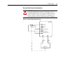
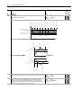
Dynamic Brake Resistor Considerations
!
ATTENTION: The drive does not offer protection for
externally mounted brake resistors. A risk of fire exists if
external braking resistors are not protected. External resistor
packages must be self-protected from over temperature or a
circuit equivalent to the one shown below must be supplied.
Figure 1.6 External Brake Resistor Circuitry
AC Drive
TB1-T7
DB Resistor
Thermostat
TB1-T8
Enable
Input #1
TB1-T9
Logic Common
TB1-T10
24V dc Power
TB1-T11
24V dc Common
BR1
BR2
Fuse
DB Resistor
Fuse
1-15
1-16
Installation/Wiring
Using Input/Output
Contactors
!
!
!
Disconnecting MOVs and
Common Mode Capacitors
ATTENTION: A contactor or other device that routinely
disconnects and reapplies the AC line to the drive to start and stop
the motor can cause drive hardware damage. The drive is
designed to use control input signals that will start and stop the
motor. If an input device is used occasionally, an auxiliary contact
on that device should also be wired to a digital input programmed
as a “Enable” function. The input device must not exceed one
operation per minute or drive damage will occur.
ATTENTION: The drive start/stop control circuitry includes
solidstate components. If hazards due to accidental contact with
moving machinery or unintentional flow of liquid, gas or solids
exist, an additional hardwired stop circuit may be required to
remove the AC line to the drive. When the AC line is removed,
there will be a loss of any inherent regenerative braking effect that
might be present - the motor will coast to a stop. An auxiliary
braking method may be required.
ATTENTION: To guard against drive damage when using
output contactors, the following information must be read and
understood. One or more output contactors may be installed
between the drive and motor(s) for the purpose of disconnecting
or isolating certain motors/loads. If a contactor is opened while
the drive is operating, power will be removed from the respective
motor, but the drive will continue to produce voltage at the output
terminals. In addition, reconnecting a motor to an active drive (by
closing the contactor) could produce excessive current that may
cause the drive to fault. If any of these conditions are determined
to be undesirable or unsafe, an auxiliary contact on the output
contactor should be wired to a drive digital input that is
programmed as “Enable.” This will cause the drive to execute a
coast-to-stop (cease output) whenever an output contactor is
opened.
PowerFlex 700S drives contain protective MOVs and common mode
capacitors that are referenced to ground. To guard against drive damage,
these devices should be disconnected if the drive is installed on an
ungrounded distribution system where the line-to-ground voltages on any
phase could exceed 125% of the nominal line-to-line voltage. To disconnect
these devices, remove the jumper(s) listed in Table 1.D. Jumpers can be
removed by carefully pulling the jumper straight out. See the PowerFlex
Reference Manual Vol. 2 for more information on ungrounded system
installation.
Installation/Wiring
!
1-17
ATTENTION: To avoid an electric shock hazard, verify that the
voltage on the bus capacitors has discharged before removing/
installing jumpers. Measure the DC bus voltage at the +DC & –
DC terminals of the Power Terminal Block. The voltage must be
zero.
Table 1.D Jumper Removal
Frames Jumper
1
PEA
2-4
PEB
PEA
5
PEB
Wire
Component
Common
Mode
Capacitors
MOV’s
Common
Mode
Capacitors
MOV’s
Common
Mode
Capacitors
MOV’s
Input Filter
Capacitors
6
Wire
Common
Mode
Capacitors
MOV’s
Input Filter
Capacitors
Jumper Location
Remove the Control Assembly and Cassette.
Jumpers are located on the drive Power Board (see
Figure 1.7).
Jumpers are located above the Power Terminal Block
(see Figure 1.7).
No.
➊
➋
➌
➍
Remove the I/O Cassette. The green/yellow jumper is ➎
located on the back of chassis in the area shown (see
Figure 1.7). Disconnect, insulate and secure the wire
to guard against unintentional contact with chassis or
components.
Note location of green/yellow jumper wire in Figure
1.7. Disconnect, insulate and secure the wire guard
against unintentional contact with chassis or
components.
Remove the wire guard from the Power Terminal
Block. Disconnect the three green/yellow wires from
the two “PE” terminals shown in Figure 1.4. Insulate
and secure the wires to guard against unintentional
contact with chassis or components.
➏
Please
refer to
Power
Terminal
Blocks,
Frame 6
on page
1-13.
1-18
Installation/Wiring
Figure 1.7 Typical Jumper Locations
Frame 1
(Control Assembly and I/O
Cassette Removed)
➌
Frame 2
➍
PE 1
PE 2
MOV-PE JMPR
PE 4
PE 3
DC FILTER CAP-PE JMPR
!
ly
On
ire
CW G
e 75
Us #14 AW
lbs
#10- 7 into
ue
Torq
AUX IN+ AUX OUT–
BR1
BR2
DC+
DC–
PE
SHLD
U/T1
V/T2
3
W/T
R/L1
S/L2
T/L3
➊
➋
Frame 5
SHLD
➎
Frames 3 & 4
➌
Optional
Communications
Module
➍
Optional
Communications
Module
300 VDC EXT PWR SPLY TERM (PS+, PS-)
POWER TERMINAL RATINGS
WIRE RANGE: 14-1/0 AWG (2.5-35 MM2)
TORQUE: 32 IN-LB (3.6 N-M)
STRIP LENGTH: 0.67 IN (17 MM)
USE 75 C CU WIRE ONLY
PE B
PE A
WIRE RANGE: 22-10 AWG (0.5-4 MM2)
TORQUE: 5.3 IN-LB (0.6 N-M)
STRIP LENGTH: 0.35 IN (9 MM)
9
17
GROUND TERMINAL RATINGS (PE)
WIRE RANGE: 6-1/0 AWG (16-35 MM2)
TORQUE: 44 IN-LB (5 N-M)
STRIP LENGTH: 0.83 IN (21 MM)
21
OUTPUT
12 IN. LBS.
1.4 N-M } TORQUE
AUX IN
+ –
POWER
75C Cu Wire
2
3 AWG [25MM ] Max.
16 IN. LBS.
1.8 N-M } TORQUE
CONTROL
WIRE
STRIP
BR1 BR2
75C Cu Wire
6 AWG [10MM2] Max.
BR1 BR2 DC+ DC- U/T1 V/T2 W/T3 R/L1 S/L2 T/L3
PE
SHLD
SHLD
➏
INPUT AC
POWER
CONTROL
WIRE
STRIP
75C Cu Wire
6 AWG [10MM2] Max.
12 IN. LBS.
1.4 N-M } TORQUE
ER
NG
DA
Installation/Wiring
I/O Wiring
1-19
Important points to remember about I/O wiring:
• Always use copper wire.
• Wire with an insulation rating of 600V or greater is recommended.
• Control and signal wires should be separated from power wires by at
least 0.3 meters (1 foot).
Important: I/O terminals labeled “(–)” or “Common” are not referenced to
earth ground and are designed to greatly reduce common mode
interference. Grounding these terminals can cause signal noise.
Table 1.E Recommended Control Wire
Type
Signal
Digital I/O
Wire Type(s)
Belden 8760/9460 (or equiv.)
Description
Standard
0.750 mm2 (18 AWG),
Analog I/O
twisted pair, 100% shield
with drain (1).
Belden 8770 (or equiv.)
0.750 mm2 (18 AWG), 3
cond., shielded for remote
pot only.
Encoder/ Less than or equal to 30 m (98 0.196 mm2 (24 AWG),
Pulse I/O ft.) – Belden 9728(or equiv.)
individually shielded.
Greater than 30 m (98 ft.) –
0.750 mm2 (18 AWG),
Belden 9773 (or equiv.)
twisted pair, shielded.
–
Unshielde Per US NEC or applicable
d
national or local code
Shielded Multi-conductor shielded cable 0.750 mm2 (18 AWG), 3
such as Belden 8770 (or equiv.) conductor, shielded.
Insulation
Rating
300V,
75-90o C
(167-194o F),
Minimum
300V, 60o C
(140o F),
Minimum
EMC
Refer to EMC Instructions on page 1-35 for details.
Compliance
(1)
If the wires are short and contained within a cabinet which has no sensitive circuits, the use of shielded wire may
not be necessary, but is always recommended.
Installation/Wiring
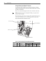
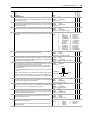
Wiring the Main Control Board I/O Terminals
Terminal blocks TB1 and TB2 contain connection points for all inputs,
outputs and standard encoder connections. Both terminal blocks reside on
the Main Control Board.
Remove the terminal block plug from the socket, and make connections.
TIP: Remember to route wires through the sliding access panel at the
bottom Control Assembly.
Reinstall the plug, when wiring is complete. The terminal blocks have keys,
which make it difficult to insert a terminal plug into the wrong socket.
Main Control Board I/O Terminal Locations
TB1
TB1 - Row T (Top)
TB1 - Row B (Bottom)
TB2
1-20
TB2 - Row T (Top)
TB2 - Row B (Bottom)
Table 1.F Main Control Board I/O Terminal Block Specifications
Name
Frame
I/O & Encoder 1-6
Blocks
(1)
Description
Signal & Encoder
power connections
Wires Size Range(1)
Maximum
Minimum
1.5 mm2
.14 mm2
(16 AWG)
(28 AWG)
Torque
Maximum
.25 N-m
(2.2 lb.-in.)
Maximum/minimum sizes the terminal block will accepts - these are not recommendations.
Recommended
.22 N-m
(1.9 lb.-in.)
Installation/Wiring
Signal
Power Supply 24V DC Return (-)
Power Supply 24V DC (+)
Logic Common
T8
Digital Input #1
T7
Enable Input
T6
Digital Output #1
T5
Digital Output #2
T4
T3
T2
T1
Digital Output Return
Thermistor Input
Thermistor Input Return
Thermistor Shield
T1
2
3
4
5
6
7
8
9
Default = Precharge
Description
Power and common for pre charge
and enable inputs.(1) Inputs may
sink or source.(2)
Rating: 100 mA maximum.
For common DC bus drives. Must
be high, for drive to complete the
pre charge cycle.
Load: 20 mA at 24V DC.
Must be high for drive to run.
Load: 20 mA at 24V DC.
24V DC open collector (sinking
logic) output.
Rating: 25 mA maximum.
24V DC open collector (sinking
logic) output.
Rating: 25 mA maximum.
Return for Digital outputs 1 and 2.
Used only in FOC2 mode with
approved motor for temperature
adaptation.
Refer to Appendix A, Specifications
for approved motors.
(1)
The drive’s 24V DC power supply supports only on-board digital inputs. Do not use it to power circuits outside of the drive.
(2)
Refer to wiring examples of sinking and sourcing outputs.
Related
Parameter
Terminal
T11
T10
T9
10
11
Table 1.G TB1 - Row T (Top) Terminals
824, 826,
827, 828,
829, 838
824, 825
824, 843,
844
824, 845,
846
485
1-21
1-22
Installation/Wiring
.
Table 1.H TB1 - Row T (Top) Wiring Examples
The following definitions are used throughout this section:
Source
A. Apply positive voltage through the device to the input or output.
B. Connect the input or output common (return) directly to the power supply common.
Sinking
A. Apply the positive voltage directly to the input or output common (return).
B. Connect the input or output to the power supply common through the device
Input/Output
Connection Example
Required Parameter Changes
Digital Inputs used for enable Sourcing Precharge and Enable Inputs - using internal power Enable - In sourcing configuration. this circuit must
and precharge control.
supply
connect to 24V DC power for drive to run.
11
Note:
24V DC Supply - supports
only on-board digital inputs.
Do not use for circuits outside
the drive.
Precharge
Precharge control is used in common bus
configurations and is not required for AC fed drives.
10
9
8
7
PRECHARGE
ENABLE
Default If this is not used the drive must
be re-programmed or use a
jumper between terminal #8 & 10
Fixed - If this is not
used a jumper must be
used between 7 & 10.
If precharge is needed, in sourcing configuration,
this circuit must connect to 24V DC power for drive
to complete the precharge cycle.
Sourcing Precharge and Enable Inputs - using external power
COMMON
(RETURN)
9
8
7
PRECHARGE
ENABLE
If precharge control is not required, reprogram Par
838 [DigIn 1 Sel] to a value of zero or replace the
contact shown with a jumper from Terminal 8 to
Terminal 10.
+24V DC
Installation/Wiring
1-23
Table 1.H TB1 - Row T (Top) Wiring Examples
Input/Output
Connection Example
Sinking Precharge and Enable Inputs - using internal power
supply
Required Parameter Changes
Enable - In sinking configuration. this circuit must
connect to 24V DC return for drive to run.
11
Precharge
Precharge control is used in common bus
configurations and is not required for AC fed drives.
10
9
8
7
PRECHARGE
If precharge control is not required, reprogram Par
838 [DigIn 1 Sel] to a value of zero or replace the
contact shown with a jumper from Terminal 8 to
Terminal 11.
ENABLE
Sinking Precharge and Enable Inputs - using external power
supply
+24V DC
9
8
7
If precharge is needed, in sinking configuration,
this circuit must connect to 24V DC return for drive
to complete the precharge cycle.
Common
(Return)
Precharge
Enable
Digital Outputs - 24V DC
outputs 25 mA maximum per
output
Digital Output 1 Indicating Alarm and Digital Output 2
Indicating Fault - in sourcing configuration
11
10
• Link Parameter 155 [Logic Status], the source,
to Parameter 845 [DigOut 2 Data], the sink
Set Parameter 846 [DigOut 2 Bit] to a value of
seven, so that Parameter 155 [Logic Status] / bit 7
[Faulted] will control the output
6
5
4
Digital Output - 24V DC
output 25 mA maximum per
output.
If one (1) output is configured
in sinking, the other output is
not available.
• Link Parameter 155 [Logic Status], the source,
to Parameter 843 [DigOut 1 Data], the sink
• Set Parameter 844 [DigOut 1 Bit] to a value of
eight, so that parameter 155 [Logic Status] / bit 8
“Alarm” will control the output
Digital Output 1 Indicating Alarm Fault - in sinking
configuration
11
10
6
4
Alarm
• Link Parameter 155 [Logic Status], the source,
to Parameter 843 [DigOut 1 Data], the sink
Set Parameter 844 [DigOut 1 Bit] to a value of 8, so
that Parameter 155 [Logic Status] / bit 8 “Alarm”
will control the output
1-24
Installation/Wiring
Signal
Analog Input #1 (-)
Analog Input #1 (+)
B9
Analog Input Shield
B8
B7
Analog Input #2 (-)
Analog Input #2 (+)
B6
B5
Analog Output #1 (+)
Analog Output #1 Return (-)
B4
Analog Output Shield
B3
B2
Analog Output #2 (+)
Analog Output #2 Return (-)
B1
Analog Output Shield
B1
2
3
4
5
6
7
8
9
10
11
Terminal
B11
B10
Description
+/-10.0V DC or +/-1.0V DC bipolar,
differential input. (1) 13 bit + sign,
20k ohm input impedance
Optional connection point for
analog input shield. (2)
+/-10.0V DC or +/-1.0V DC bipolar,
differential input. (1) 13 bit + sign,
20k ohm input impedance
+/-10.0V DCDC bipolar, differential
output, 11 bit + sign, 2k ohm
minimum load
Optional connection point for
analog output shield. (2)
+/-10.0V DC bipolar, differential
output, 11 bit + sign, 2k ohm
minimum load
Optional connection point for
analog shields.
Related
Parameter
Table 1.I TB1 - Row B (Bottom) Terminals
800, 802,
803, 804,
805
806, 808,
809, 810,
811
812, 814,
815, 817,
818
813, 819,
820, 822,
823,
(1)
Refer to Analog Input Settings on page 1-32 for necessary dip switch settings.
(2)
Analog shields should connect to common at the signal source, if possible. Shields for signals from ungrounded devices, such as analog
tachometers, should connect to an analog shield terminal point at the drive.
Installation/Wiring
1-25
Table 1.J TB1 - Row B (Bottom) Wiring Examples
Input/Output
Connection Example
Analog Inputs
Analog Inputs for Speed Reference and Speed Trim - shield
+/-10V DC or +/-1.0V DC
terminated at source
(DIP switch selectable)
11
Terminate shields at the analog
Speed
10
#1
+
source if analog common is
Reference
COMMON
available
(RETURN)
8
Used for Speed Reference and
Speed Trim
Analog Outputs
+/-10V DC or +/-1.0V DC
Used to drive analog meters
displaying speed and current
7
+
Analog Inputs for Speed Reference and Speed Trim - shield
terminated at drive
11
10
+
Speed Reference
0-10V dc = 0-100%
of Motor Base Speed
+
Speed Trim
0-10V dc = 0-10%
Trim
9
8
7
Analog Outputs
+/-10V DC
#2 Speed
Trim
COMMON
(RETURN)
Analog Outputs Indicating Motor Speed and Motor Current
6
#1 Motor
Speed
+
-
5
4
3
2
1
Motor
#2 Current
+
-
Required Parameter Changes
Using Analog In1 as 0-10V speed reference
• Adjust Parameter 803 [Anlg In1 Offset] so that
the minimum analog signal creates the minimum
speed reference (if the minimum input is 0V DC
and the minimum speed reference is zero, enter
a value of zero)
• Adjust the Parameter 802 [Anlg In1 Offset] so
that the maximum analog signal creates the
maximum speed reference (if the maximum
input is 10V DC and the maximum speed
reference is motor base speed, enter a value of
0.1)
• Send the data to the Speed Reference
parameter
Par 10 [Speed Ref1] (the destination) linked to
Par 800 [Anlg In1 Data] (the source)
• Select Ref 1 as the active speed ref Par 16
[Speed Ref Sel] = 1
• Par 153 [Control Option]/bit 0 = 0 Unipolar
Speed Reference”
Using Analog In2 as -10 to +10V speed trim @
10%:
• Adjust Parameter 809 [Anlg In2 Offset] so that
the minimum analog signal creates the minimum
speed trim (if the minimum input is 0V DC and
the minimum trim is zero, enter a value of zero)
• Adjust Parameter 808 [Anlg In2 Offset] so that
the maximum analog signal creates the
maximum speed trim (if the maximum input is
10V DC and the maximum speed trim is 10%,
enter a value of 0.01)
• Send the data to the speed Reference
parameter
Par 13 [Speed Ref2] (the destination) linked to
Par 806 [Anlg In2 Data] (the source)
• Select Ref 1 as the active speed ref and Ref2 as
trim [Speed Ref Sel] = 3
Using Analog Out 1, -10V to +10V to meter
Motor RPM and direction:
• Adjust Parameter 812 [Anlg Out1 Offset] so that
minimum speed creates a minimum signal (if the
minimum speed is zero and the minimum signal
is zero, enter a zero)
• Adjust Parameter 817 [Anlg Out1 Scale] so that
the maximum speed creates a maximum signal
(if the maximum speed is 100% of motor base
speed and the maximum signal is 10V DC, enter
a value of 0.1)
• Send the data to the Analog Output
Par 815 [Anlg Out1 Real] (the destination) linked
to Par 300 [Motor Spd Fdbk] (the source)
Using Analog Out 2, -10V to +10V to meter
Motor Current
• Adjust Parameter 813 [Anlg Out2 Offset] so that
minimum current creates a minimum signal (if
the minimum current is zero and the minimum
signal is zero, enter a zero)
• Adjust Parameter 822 [Anlg Out2 Scale] so that
the maximum current creates a maximum signal
(if the maximum current is 200% of motor NP
FLA and the maximum signal is 10V DC, enter a
value of 2.0)
• Send the data to the Analog Output
Par 820 [Anlg Out2 Real] (the destination) linked
to Par 308 [Output Current] (the source)
• Scale the Output to the source parameter
Par 822 [Anlg Out2 Scale] = xx (Par2 [Motor NP
FLA]/10V Output
Installation/Wiring
Table 1.K TB2 - Row T (Top) Terminals
T1
Terminal
T13
T12
T11
T10
T9
T8
T7
T6
T5
T4
T3
T2
T1
Signal
Encoder Signal A
Encoder Signal Not A
Encoder Signal B
Encoder Signal Not B
Encoder Signal Z
Encoder Signal Not Z
Shield
Digital Input #2
Digital Input #2 Return
2
3
4
5
6
7
8
9
10 11 12 13
Description
Primary encoder interface. 5 or 12V
DC switch selectable (1), Nominal
current draw per channel @ 12V
DC 45 mA, @5V DC 32 mA
Maximum input frequency for
Encoders 0 & 1 is 500 kHz.
Related
Parameter
1-26
222, 230,
231, 232,
233, 234,
235, 236,
237, 238
Connection point for encoder shield.
High speed 12-24V DC sinking
824, 830,
digital input.
831, 832,
833, 839
Digital Input #3
High speed 12-24V DC sinking
824, 834,
digital input.
835, 836,
Digital Input #3 Return
837, 840
Power Supply +12V DC (A) (+)
12V DC power supply for primary
high speed
Power Supply +12V DC Return (A) (-) encoder interface and (2)
inputs. Rating 300 mA
(1)
Refer to Encoder Input Settings on page 1-32 for necessary dip switch settings.
(2)
This power supply supports only the primary encoder interface and digital inputs. Do not use it to power circuits
outside of the drive.
Installation/Wiring
1-27
Table 1.L TB2 - Row T (Top) Wiring Examples
Input/Output
Primary Encoder Interface Supports 12V DC differential
encoders with internal power
supply.
5V DC differential encoders
require external power supply
and special jumper settings.
Refer to Main Control Board I/O
Configuration Settings on
page 1-32.
Connection Examples
Primary Encoder - using internal power supply
1
2
Power
Common
(Return)
7
8 9 10 11 12 13
Z Z B B A A
Case Ground
Primary Encoder - using external power supply
7
8 9 10 11 12 13
Shield
Power
Common
(Return)
Power
Common
(Return)
Z Z B B A A
Case Ground
Required Parameter Changes
• Set the value of Parameter 222 [Motor Fdbk
Sel] to a value of 0 - Encoder 0, so the drive will
use this encoder as the primary motor speed
feedback device.
• Set the value of Parameter 232 [Encoder0 PPR]
to match the encoder’s resolution.
1-28
Installation/Wiring
Table 1.L TB2 - Row T (Top) Wiring Examples
Input/Output
High Speed Inputs
12 or 24V DC
Connection Examples — 3-Wire Control
Sourcing High Speed Inputs, Used for 3 Wire Control - using
the internal power supply
1 2 3 4 5 6 7
Required Parameter Changes
• Set the value of Parameter 839 [DigIn 2 Sel] to
a value of 1 - Normal Stop
• Set the value of Parameter 840 [DigIn 3 Sel] to
a value of 2 - Start
• Set Parameter 153 [Control Options] / bit 8
“3WireControl”
Start
Stop
Sourcing High Speed Inputs, Used for 3 Wire Control - using an Note: +12V and +24V are also available from
external power supply
TB1 Top 10 & 11.
EXTERNAL
POWER SUPPLY
POWER COMMON
(RETURN)
3 4 5 6 7
Start
Stop
Sinking High Speed Inputs, Used for 3 Wire Control - using the
internal power supply
1 2 3 4 5 6
Start
Stop
Sinking High Speed Inputs, Used for 3 Wire Control- using an
external power supply
24V DC
COMMON
(RETURN)
EXTERNAL 24V
POWER SUPPLY
3 4 5 6
Start
Stop
Note: +12V and +24V are also available from
TB1 Top 10 & 11.
Installation/Wiring
1-29
Table 1.L TB2 - Row T (Top) Wiring Examples
Input/Output
High Speed Inputs
12 or 24V DC
Connection Examples — 2-Wire Control
Sourcing High Speed Inputs, Used for 2 Wire Control - using
the internal power supply
1 2 3
5 6 7
Required Parameter Changes
• Set the value of Parameter 839 [DigIn 2 Sel] to
a value of 3 - Run
• Set Parameter 153 [Control Options] / bit 9 “2W
Coast Stop” to make the drive coast stop when
input 2 goes low
• Reset Parameter 153 [Control Options] / bit 9
“2W Coast Stop” to make the drive ramp stop
when input 2 goes low
• Reset Parameter 153 [Control Opt]/bit 8 “3Wire
Control” for two wire control
Run-Stop
Sourcing High Speed Inputs, Used for 2 Wire Control - using an Note: +12V and +24V are also available from
external power supply
TB1 Top 10 & 11.
12 or 24V dc
Power Supply
Common
Power
(Return)
3
5 6
Run-Stop
Sinking High Speed Inputs, Used for 2 Wire Control - using the
internal power supply
1 2 3 4 5 6
Run Stop
Sinking High Speed Inputs, Used for 2 Wire Control - using an Note: +12V and +24V are also available from
TB1 Top 10 & 11.
external power supply
24V DC
COMMON
(RETURN)
EXTERNAL 24V
POWER SUPPLY
1 2 3 4 5 6
Run Stop
Installation/Wiring
Table 1.M TB2 - Row B (Bottom) Terminals
B1
2
3
4
5
6
7
8
9
10 11 12 13
Terminal
B13
B12
B11
B10
B9
B8
Signal
Encoder Signal A
Encoder Signal Not A
Encoder Signal B
Encoder Signal Not B
Encoder Signal Z
Encoder Signal Not Z
Description
Secondary encoder interface.
5 or 12V DC switch
selectable (1), Nominal
current draw per channel @
12V DC 45 mA, @5V DC 32
mA
Maximum input frequency for
Encoders 0 & 1 is 500 kHz.
Connection point for encoder
shield.
B7
Shield
B6
B5
B4
Unused
Relay Output
Relay Output Return
B3
B2
B1
Unused
Power Supply +12V DC (B) (+)
12V DC power supply for
interface.
Power Supply +12V DC Return (B) (-) secondary encoder
Rating 300 mA(2)
Relay contact output.
Rating: 5A @ 24V DC
Resistive, 2A 24V DC
Inductive
Related
Parameter
1-30
222, 240,
241, 242,
243, 244,
245, 246,
247, 248
824, 841,
842
(1)
Refer to Encoder Input Settings on page 1-32 for necessary dip switch settings.
(2)
This power supply supports only the secondary encoder interface. Do not use it to power circuits outside of the
drive
Installation/Wiring
1-31
Table 1.N TB2 - Row B (Bottom) Wiring Examples
Input/Output
Connection Example
Secondary Encoder Interface Secondary Encoder - using internal power supply
- Supports 12V DC differential
encoders with internal power
supply.
5V DC differential encoders
require external power supply
and special jumper settings.
Refer to Main Control Board I/O
Configuration Settings on
page 1-32.
1
2
Power
Common
(Return)
7
8 9 10 11 12 13
Required Parameter Changes
• Set the value of Parameter 222 [Motor Fdbk
Sel] to a value of 1 - Encoder 1, so the drive will
use this encoder as the primary motor speed
feedback device
• Set the value of Parameter 242 [Encoder1 PPR]
to match the encoder’s resolution
Z Z B B A A
Case Ground
Secondary Encoder - using external power supply
7
8 9 10 11 12 13
Shield
Power
Common
(Return)
Power
Common
(Return)
Auxiliary Output - Relay
contact output
Z Z B B A A
Case Ground
Auxiliary Output, Used to Indicate Running
EXTERNAL
24V DC
COMMON
(RETURN)
EXTERNAL 24V
POWER SUPPLY
4
5
Running
• Link Parameter 155 [Logic Status], the source,
to Parameter 841 [Relay Out Data], the sink
• Set Parameter 842 [Relay Out Bit] to a value of
one, so that Parameter 155 [Logic Status] / bit 1
“Running” will control the output.
1-32
Installation/Wiring
Main Control Board I/O Configuration Settings
Figure 1.8 Main Control Board Dip Switches
SW1
SIDE VIEW
FRONT - TOP VIEW
UP = OPEN = OFF
1 2
DOWN = CLOSED= ON
SW2
SIDE VIEW
FRONT - TOP VIEW
UP = OPEN = OFF
OPEN
1 2 3 4 5 6 7 8
DOWN = CLOSED= ON
Analog Input Settings
Switch SW1-1 configures the scaling of Analog Input #1. Switch SW1-2
configures the scaling of Analog Input #2. Open the switch for +/-10.0V DC
operation. Close the switch for +/-1.0V DC operation.
Table 1.O Analog Input #1 Switch Settings For Scaling
Analog Input #1 Scaling
SW1-1
+/-10.0V DC
Open
+/-1.0V DC
Closed
Table 1.P Analog Input #2 Switch Setting For Scaling
Analog Input #2 Scaling
SW1-2
+/-10.0V DC
Open
+/-1.0V DC
Closed
Encoder Input Settings
Dip switch SW2 on the main control board configures the encoder inputs
for 5V DC or 12V DC operation. Switches SW2-2, 4, and 6 are for the
primary encoder. Set these switches to match the encoder output
specifications. Open these switches for 12V DC operation, close them for
5V DC operation.
Table 1.Q SW2 - Primary Encoder Input Configuration
Primary Encoder
5V DC Operation
12V DC Operation
SW2-2
Closed
Open
SW2-4
Closed
Open
SW2-6
Closed
Open
Installation/Wiring
1-33
Dip switch SW2 on the main control board configures the encoder inputs
for 5V DC or 12V DC operation. Switches SW2-1, 3, and 5 are for the
secondary encoder. Set these switches to match the encoder output
specifications. Open these switches for 12V DC operation, close them for
5V DC operation.
Table 1.R SW2 - Secondary Encoder Input Configuration
Secondary Encoder
5V DC Operation
12V DC Operation
Connecting SynchLink
SW2-1
Closed
Open
SW2-3
Closed
Open
SW2-5
Closed
Open
SynchLink provides high-speed synchronization and communication
between multiple PowerFlex 700S drives (or other products with SynchLink
capability).
Refer to The SynchLink Design Guide, publication # 1756-TD008 when
planning and connecting the SynchLink network.
Class 1 LED Product
!
ATTENTION: Hazard of permanent eye damage exists when
using optical transmission equipment. This product emits intense
light and invisible radiation. Do not look into module ports or
fiber optic cable connectors.
Figure 1.9 SynchLink Connections
J8 (Transmit)
J9 (Receive)
1-34
Installation/Wiring
Connect cables to J9 (receive) and J8 (transmit) connectors on the bottom of
the Main Control Board. Push the plug into the socket until it produces an
audible click.
Important: Do not overtighten tie-wraps.
Table 1.S SynchLink Cables and Accessories
Description
2 x 25 cm Fiber Optic Link
2 x 1 M Fiber Optic Link
2 x 3 M Fiber Optic Link
2 x 5 M Fiber Optic Link
10 M Fiber Optic Link
20 M Fiber Optic Link
50 M Fiber Optic Link
100 M Fiber Optic Link
250 M Fiber Optic Link
500 M Fiber Optic Bulk
SynchLink Fiber-Hub, 1 input, Base
SynchLink Fiber-Hub, 4 output, “Star” Splitter
SynchLink Bypass Switch
Cat. No.
1403-CF000
1403-CF001
1403-CF003
1403-CF005
1403-CF010
1403-CF020
1403-CF050
1403-CF100
1403-CF250
1403-CFBLK
1751-SLBA
1751-SL4SP
1751-SLBP/A
Table 1.T Fiber Optic Cable Assembly
Specification
Connecting Cables
200/230 micron HCS (Hard Clad Silica)
• Versalink V-System
• Lucent Technologies,
• Specialty Fibers Technology Division
300 meters with no more than one splice or one adapter
Maximum
Cable Length
Minimum
1 meter
Cable Length
Minimum inside bend radius 25.4mm (1 in.) Any bends with a shorter inside radius can permanently
damage the fiber optic cable. Signal attention increases with
decreased inside bend radius.
Operating Wavelength
650 nm (Red)
Data Rate
5 Mbps
Maximum
• 10 - Daisy Chain
Node Count
• 256 - Star Configuration
Installation/Wiring
EMC Instructions
1-35
CE Conformity
Conformity with the Low Voltage (LV) Directive and Electromagnetic
Compatibility (EMC) Directive has been demonstrated using harmonized
European Norm (EN) standards published in the Official Journal of the
European Communities. PowerFlex Drives comply with the EN standards
listed below when installed according to the User and Reference Manual.
Declarations of Conformity are available online at:
http://www.ab.com/certification/ce/docs.
Low Voltage Directive (73/23/EEC)
• EN50178 Electronic equipment for use in power installations.
EMC Directive (89/336/EEC)
• EN61800-3 Adjustable speed electrical power drive systems Part 3:
EMC product standard including specific test methods.
General Notes
• If the adhesive label is removed from the top of the drive, the drive must
be installed in an enclosure with side openings less than 12.5 mm (0.5
in.) and top openings less than 1.0 mm (0.04 in.) to maintain compliance
with the LV Directive.
• The motor cable should be kept as short as possible in order to avoid
electromagnetic emission as well as capacitive currents.
• Use of line filters in ungrounded systems is not recommended.
• PowerFlex drives may cause radio frequency interference if used in a
residential or domestic environment. The user is required to take
measures to prevent interference, in addition to the essential
requirements for CE compliance listed below, if necessary.
• Conformity of the drive with CE EMC requirements does not guarantee
an entire machine or installation complies with CE EMC requirements.
Many factors can influence total machine/installation compliance.
• PowerFlex drives can generate conducted low frequency disturbances
(harmonic emissions) on the AC supply system. More information
regarding harmonic emissions can be found in the PowerFlex Reference
Manual Vol. 2.
Installation/Wiring
Essential Requirements for CE Compliance
Conditions 1-6 listed below must be satisfied for PowerFlex drives to meet
the requirements of EN61800-3.
3. Standard PowerFlex 700S CE compatible Drive.
4. Review important precautions/attentions statements throughout this
document before installing drive.
5. Grounding as described on page 1-4.
6. Output power, control (I/O) and signal wiring must be braided, shield
cable with a coverage of 75% or better, metal conduit or equivalent
attenuation.
7. All shielded cables should terminate with proper shielded connector.
8. Conditions in Table 1.U on page 36
Table 1.U PowerFlex 700S EN61800-3 EMC Compatibility
Frame
1-36
1
2
3
4
5
6
Second Environment
Restrict Motor Cable to 30 m
(98 ft.)
Any Drive and Option
✔
✔
✔
✔
✔
✔
First Environment
Restricted Distribution
Refer to
PowerFlex Reference Manual
Vol. 2
Chapter
2
Start-Up
This chapter describes how you start-up the PowerFlex 700S Drive. Refer to
Appendix D for a brief description of the HIM (Human Interface Module).
For Information on …
Prepare for Drive Start-Up
Status Indicators
Assisted Start-Up
!
Prepare for Drive Start-Up
See Page...
2-1
2-3
2-4
ATTENTION: Power must be applied to the drive to perform
the following start-up procedure. Some of the voltages present are
at incoming line potential. To avoid electric shock hazard or
damage to equipment, only qualified service personnel should
perform the following procedure. Thoroughly read and
understand the procedure before beginning. If an event does not
occur while performing this procedure, Do Not Proceed.
Remove Power including user supplied control voltages. User
supplied voltages may exist even when main AC power is not
applied to then drive. Correct the malfunction before continuing.
Before Applying Power to the Drive
❏ 1. Confirm that motor wires are connected to the correct terminals and are
secure. Confirm Frame 5 transformer connections (refer to page 1-9).
❏ 2. Confirm that encoder wires are connected to the correct terminals and
are secure.
❏ 3. Confirm that all control inputs are connected to the correct terminals and
are secure.
❏ 4. Verify that AC line power at the disconnect device is within the rated
value of the drive.
❏ 5. Verify that control power voltage is correct.
The remainder of this procedure requires that a HIM be installed. If an
operator interface is not available, remote devices should be used to start-up
the drive.
2-2
Start-Up
Applying Power to the Drive
❏ 6. Apply AC power and control voltages to the drive. Examine the Power
(PWR) LED.
Steady Green
Power has been applied to the drive and no faults are present.
❏ 7. Examine the Status (STS) LED. Verify that it is flashing green. If it is not
in this state, check the following possible causes and take the necessary
corrective action.
Flashing Yellow
A run inhibit exists in the drive. Refer to Chapter 4 to correct the problem.
Flashing Red
A fault has occurred. Refer to Table 4.C on page 4-4 for drive faults and
actions to correct the problem.
If any digital input is configured to Stop – CF (CF = Clear Fault) or Enable,
verify that signals are present or the drive will not start. Refer to Chapter 4
for a list of potential digital input conflicts.
If a fault code appears, refer to Chapter 4.
If the STS LED is not flashing green at this point, refer to the Status
Indicators descriptions in Table 2.A on page 2-3.
❏ 8. Proceed to Start-Up Routine.
Start-Up
Status Indicators
2-3
Figure 2.1 Drive Status Indicators
4
DRIVE
DRIVE
1
ENABLE
SYNCHLINK
2
3
Table 2.A Drive Status Indicator Descriptions
#
Color
State
Description
➊ PWR
Name
Green
Steady
Illuminates when power is applied to the drive.
➋
Green
Flashing
Steady
Flashing
DRIVE
Control Assembly
Control
Communications
Power Structure
(Power)
STS (Status)
➌ PORT
MOD
NET A
NET B
Drive ready, but not running & no faults are present.
Drive running, no faults are present.
Yellow
A type 2 (non-configurable) alarm condition exists, drive continues to
run.
Steady
A type 1 (user configurable) alarm condition exists, but drive
continues to run.
Red
Flashing
A fault has occurred.
Steady
A non-resettable fault has occurred.
Red /
Flashing
The drive is in flash recovery mode. The only operation permitted is
Yellow Alternately flash upgrade.
Status of DPI port internal communications (if present).
Status of communications module (when installed).
Refer to the
Communication
Status of network (if connected).
Adapter User Manual Status of secondary network (if connected).
➍ SYNCHLINK Green
ENABLE
Steady
Green
Red
Flashing
Flashing
Green
Green
On
Off
• The module is configured as the time keeper
or
• The module is configured as a follower and synchronization is
complete.
The follower(s) are not configured with the time keeper.
• The module is configured as a time master on SynchLink and has
received time information from another time master on SynchLink.
The drive’s enable input is high.
The drive’s enable input is low.
2-4
Start-Up
Assisted Start-Up
This routine prompts you for information needed to start-up a drive for most
applications, such as line and motor data, commonly adjusted parameters
and I/O.
Important: This start-up routine requires a HIM. If the drive is configured for 2-wire
control, the HIM installed on the drive will also act as a 2-wire device. In
2-wire mode, the drive will start when the HIM “Start” is pressed and
stop when the HIM “Start” is released. The recommended mode of use
for the Start-Up Routine is 3-wire control, Parameter 153 [Control
Options], Bit 8 set to “1”.
The assisted start-up routine asks simple yes or no questions and prompts
you to input required information. Access Assisted Start-Up by selecting
“Start-Up” from the Main Menu.
Step
Key(s)
Example LCD Displays
1. To exit the User Display screen, Press Esc.
Esc
F
Stopped
0.0
Auto
RPM
0.0
0.0 Output
DC Bus V
1. In the Main Menu, use the Down Arrow to scroll to
“Start Up”
2. Press Enter.
TIP: Throughout the Start-Up Routine many screens
have more selection than shown. Use the arrow keys
to scroll through all the menu options.
1. Follow the instructions on the screen to complete
the Start-Up.
F
Stopped
Auto
RPM
Main Menu:
0.0
Diagnostics
Parameter
Device Select
PowerFlex 700S
Start-Up
The Start-Up
routine sets up
0.0 for
the drive
Diagnostics
basic operation.
Push Enter.
Important: If using a HIM the following functions are not available.
• Alt-Man
• Alt-Lang
• Alt-SMART
0.0
C
Start-Up
2-5
Table 2.B Start-Up Menu
PowerFlex 700S
Start-Up
Down 1 level or Select
Back 1 level or 1 selection
Scroll all choices
Esc
Feedback
Configuration
Motor Control
Motor Data
Power Circuit Test
Direction Test
Select Motor Control
Mode
Select DB Resistor
Enter Motor NP Data
Power & Units
FLA
Volts
Hertz
RPM
Poles
Setup / Select
Encoder
Resolver
Hi-Res Encoder
Linear Sensor
Diagnostic Check for
Drive Power Circuit
Verify Direction
Motor Tests
Inertia Measure
Speed Limits
Speed Control
Start / Stop / I/O
Field Oriented
Control: Measure
Stator Resistance,
Leakage Inductance,
Magnetizing
Inductance
PMag Motor: Encoder
Offset, Stator
Resistance, Stator
Inductance, Back EMF
Measure System
Inertia
Select Direction
Control
Set FWD, REV and
ABS Speed Limits
Select Sources For All
Speed References
Configure:
Digital Inputs, Digital
Outputs, Analog
Inputs, Analog Outputs
Done /
Exit
Note: In 2-wire mode, the drive will start when the HIM “Start” is pressed
and stop when the HIM “Start” is released. The recommended mode
of use for the Start-Up Routine is 3-wire control, Parameter 153
[Control Options], Bit 8 set to “1”.
2-6
Notes:
Start-Up
Chapter
3
Programming and Parameters
Chapter 3 provides a complete listing and description of the PowerFlex
700S parameters. The parameters can be programmed (viewed/edited) using
a HIM (Human Interface Module). As an alternative, programming can also
be performed using DriveTools 2000™ software and a personal computer.
For information on...
About Parameters
How Parameters are Organized
Parameter Data in Linear List Format
Parameter Cross Reference By Name
About Parameters
See page
3-1
3-3
3-16
3-94
To configure a Drive module to operate in a specific way, drive parameters
may have to be set. Three types of parameters exist:
•ENUM Parameters
These parameters allow a selection from 2 or more items
•Bit Parameters
These parameters have individual bits associated with features or
conditions. If the bit is 0, the feature is off or the condition is false. If
the bit is 1, the feature is on or the condition is true.
•Numeric Parameters
These parameters have a single numeric value (i.e. 0.1 Volts).
The example on the following page shows how each parameter type is
presented in this manual.
➋
➌
No.
Name
Description
Values
151
Logic Command
4
No.
➊
PM Offset En
Dir Sel En
Pwr Diag En
MC Atune En
Time Axis En
TachLoss Rst
Spd S Crv En
SpdRamp Dsbl
0 0 0 0 0 0 0
15 14 13 12 11 10 9
Mtr Inert En
Sys Inert En
Inertia Comp
Frict Comp
PositionEnbl
Reserved
Reserved
Default
Bit
ProcsTrim En
The controller-drive interface (as defined by the Controller Commmunication Format) sets bits to enable and disable various functions and algorithms. Bits that
are changed here are reflected in Parameter 152 [Applied LogicCmd]. Note: Bits 4 through 9 in Logic Command are NOT recalled from Control EEprom. They
will be cleared upon drive powerup or following an EEprom recall operation.
Options
110
Data Type
➊
Read-Write
Programming and Parameters
Linkable
3-2
0
8
0
7
0
6
0
5
0
4
0
3
0
2
0
1
0
0
Spd/Torq ModeSel
Selects the source for the drive torque reference.
Motor NP RPM
Set to the motor nameplate rated RPM.
0 = True
1 = False
Default:
Options:
1
“Speed Reg”
0
“Zero Torque”
4
“Max Spd/Torq”
1
“Speed Reg”
5
“Sum Spd/Torq”
2
“Torque Ref”
6
“AbsMn Spd/Tq”
3
“Min Spd/Torq”
Units:
RPM
✓ 16-bit
Default:
Calculated
Integer
Min/Max:
1/30000
Comm Scale: Parameter 4 [Motor NP RPM] = 1.0
Name
Description
No. - Parameter Number
Stop drive before changing this parameter
➋
➌
Name - Parameter name as it appears in DriveExecutive software.
Description - Brief description of parameter function.
Values - Define the various operating characteristics of the parameter. There are 3 types of Values.
ENUM
Default:
Lists the value assigned at the factory.
Options:
Displays the selections available.
Bit
Default:
Lists the value assigned at the factory.
Options:
Displays the selections available.
Numeric
Default
Lists the value assigned at the factory.
Min.
Displays lowest possible setting.
Max.
Displays highest possible setting.
Type
Indicates if parameter is linkable, read-write, read-only, and data type (i.e. integer, floating point,
boolean).
Comm
Value sent from Controller or Comm Device = Drive Parameter Value x Comm Scale
Scale:
Programming and Parameters
How Parameters are
Organized
DriveExecutive programming software displays parameters in “Linear List”
or “File Group Parameter” format. Viewing the parameters in “File Group
Parameter” format simplifies programming by grouping parameters that are
used for similar functions. There are twelve files. Each file is divided into
multiple groups of parameters.
Proc
or
Metering
300
72
762
310
307
308
297
311
309
547
306
312
313
345
824
168
801
807
816
821
298
299
Dyna
Moto
Monit
3-3
mic C
r Con
Motor Spd Fdbk
Scaled Spd Fdbk
Mtr Posit Fdbk
Output Freq
Output Voltage
Output Current
Output Curr Disp
Output Power
% Motor Flux
Estimated Torque
DC Bus Voltage
MotorFluxCurr FB
Heatsink Temp
Drive OL JnctTmp
Local I/O Status
StdDig I/O State
Anlg In1 Volts
Anlg In2 Volts
Anlg Out1 Volts
Anlg Out2 Volts
Elapsed Run Time
Elapsed MWHrs
trol
ontro
l
Posit
io
ess C
Torqu
ontro
e Co
l
ntrol
d Co
ntrol
Spee
Control Status
Logic State Mach
150
Logic Status
155
Logic Ctrl State
157
Run Inhibit Stat
156
Motor Ctrl Cmmd
166
Motor Ctrl Ackn
167
MC Status
555
Drive OL Status
346
DigIn ConfigStat
159
Test Status
165
SL System Time
317
Utility
Spee
d/Po
sit Fd
n Co
b
k
ntrol
Inputs
Motor Ctrl Data
Stator Frequency
533
Iqs Command
534
Mtr Vds Base
434
Mtr Vqs Base
435
Vds Fdbk Filt
441
Vqs Fdbk Filt
442
Vqs Command
541
Vds Command
542
Iqs Command
535
Ids Command
537
Iqs Feedback
539
Ids Feedback
540
Com
& Ou
tputs
Sync
munic
a
Drive Data
400
401
404
692
314
315
527
526
1001
1002
tion
hLink
Rated Amps
Rated Volts
Dead Time
DPI Baud Rate
VPL Firmware Rev
VPL Build Number
MC Firmware Rev
MC Build Number
SynchLink Rev
SL System Rev
3-4
Programming and Parameters
Spee
d/Po
Posit
sit Fd
ion C
Proc
bk
ontro
ess C
Torqu
l
ontro
Spee
e Co
l
ntrol
d Co
Dyna
ntrol
mic C
Moto
ontro
l
r Con
Monit
t
r
o
l
or
Motor Data
1
2
3
4
5
6
7
8
9
336
Motor NP Volts
Motor NP FLA
Motor NP Hertz
Motor NP RPM
Motor NP Power
Mtr NP Pwr Units
Motor Poles
Motor Inertia
Total Inertia
Service Factor
Drive Config
Motor Ctrl Mode
485
PWM Frequency
402
Voltage Class
403
Dead Time Comp
405
Line Undervolts
409
PreChrg TimeOut
410
PreChrg Control
411
FOC Mode Config
510
FOC2 Mode Config
511
Test Mode Config
514
PMag Mode Cnfg
512
PM TestWait Time
505
PM Test Idc Ramp
506
PM Test FreqRamp
507
PM Test Freq Ref
508
PM Test I Ref
509
Flux Ratio Ref
424
Tuning
423
453
454
425
426
443
470
444
500
501
437
438
439
440
469
473
449
450
451
474
475
447
448
446
445
476
472
431
432
433
477
Utility
Iqs Rate Limit
Iu Offset
Iw Offset
Flux Rate Limit
Flux Satur Coef
Flux Reg P Gain1
Flux Reg P Gain2
Flux Reg I Gain
Bus Util Limit
Torque En Dly
Vqs Max
Vds Max
Vqs Min
Vds Min
StatorInduc Gain
Freq Reg FF Gain
Freq Reg I Gain
Freq Reg P Gain
Freq Track Filt
Freq Reg We BW
Freq Reg Wr BW
Slip Reg P Gain
Slip Reg I Gain
Slip Gain Min
Slip Gain Max
Slip Gain Comp
PreCharge Delay
Test Current Ref
Test Freq Ref
Test Freq Rate
Est Theta Delay
Inputs
Com
& Ou
tputs
Sync
munic
ati
on
hLink
Autotune Results
Iqs Integ Freq
421
Iqs Reg P Gain
422
Ids Integ Freq
429
Ids Reg P Gain
430
Rated Slip Freq
486
Motor NTC Coef
487
Flux Current
488
StatorInductance
490
StatorResistance
491
Leak Inductance
492
Rotor Resistance
502
Current Reg BW
503
PM AbsEncd Offst
504
PM Motor
427
520
521
522
523
PM Mtr CEMF Comp
PM Q Inductance
PM D Inductance
PM Stator Resist
PM Mtr CEMF Coef
Programming and Parameters
Proc
Monit
Moto
Dyna
or
mic C
r Con
trol
Configuration
151
Logic Command
152
Applied LogicCmd
153
Control Options
158
Drive Logic Rslt
160
Zero Speed Lim
335
Abs OverSpd Lim
ess C
Torqu
ontro
e Co
l
ntrol
d Co
ntrol
Spee
ontro
l
Overload
337
338
339
340
343
344
OL OpnLp CurrLim
OL ClsLp CurrLim
Drive OL JnctTmp
Drive OL Status
Drive OL TP Sel
Drive OL TP Data
Spee
Posit
io
d/Po
n Co
ntrol
Utility
sit Fd
Inputs
Com
& Ou
tputs
Sync
munic
a
tion
hLink
bk
Stop/Brake Modes
414
Brake/Bus Cnfg
415
BusReg/Brake Ref
416
Brake PulseWatts
417
Brake Watts
154
Stop Dwell Time
Power Loss
406
Power Loss Mode
407
Power Loss Time
408
Power Loss Level
3-5
3-6
Programming and Parameters
Dyna
Moto
Monit
or
Reference
16
10
11
12
13
14
15
20
17
18
40
30
31
41
32
33
42
34
43
37
35
36
44
38
46
21
47
45
61
62
63
56
55
57
58
59
60
140
141
142
143
144
145
Spee
r Con
mic C
d Co
trol
Torqu
e
ontro
Speed Ref Sel
Speed Ref 1
Spd Ref1 Divide
Speed Ref 2
Spd Ref2 Multi
Speed Ref 4
Speed Ref 5
Speed Ref DPI
Jog Speed 1
Jog Speed 2
Selected Spd Ref
Rev Speed Limit
Fwd Speed Limit
Limited Spd Ref
Accel Time
Decel Time
Ramped Spd Ref
S Curve Time
S Curve Spd Ref
Spd Ref Bypass
SpdRef Filt Gain
SpdRef Filt BW
Filtered Spd Ref
Speed Ref Scale
Scaled Spd Ref
Speed Trim 1
Spd Trim1 SpdRef
Delayed Spd Ref
Virt Encoder EPR
Virt Encdr Posit
Virt Encdr Dlyed
Inertia SpeedRef
Speed Comp
InertiaAccelGain
InertiaDecelGain
Inertia Torq Add
DeltaSpeedScale
FricComp Spd Ref
FricComp Setup
FricComp Stick
FricComp Slip
FricComp Rated
FricComp TorqAdd
ntrol
Proc
Cont
ess C
Posit
io
rol
Spee
d/Po
ontro
n Co
l
ntrol
sit Fd
Utility
Inputs
Com
& Ou
tputs
bk
l
Regulator
47
22
25
26
23
24
19
30
31
301
300
93
94
71
100
89
85
84
80
81
82
87
8
9
90
97
91
92
101
102
103
86
95
96
302
Spd Trim1 SpdRef
Speed Trim 2
STrim2 Filt Gain
SpdTrim2 Filt BW
Speed Trim 3
SpdTrim 3 Scale
Atune Spd Ref
Rev Speed Limit
Fwd Speed Limit
Motor Speed Ref
Motor Spd Fdbk
SRegFB Filt Gain
SReg FB Filt BW
Filtered SpdFdbk
Speed Error
Spd Err Filt BW
Servo Lock Gain
SpdReg AntiBckup
Speed Reg Ctrl
Spd Reg P Gain
Spd Reg I Gain
SReg Torq Preset
Motor Inertia
Total Inertia
Spd Reg BW
Act Spd Reg BW
Spd Reg Damping
SpdReg P Gain Mx
SpdReg Integ Out
Spd Reg Pos Lim
Spd Reg Neg Lim
Spd Reg Droop
SRegOut FiltGain
SReg Out Filt BW
Spd Reg PI Out
Sync
munic
a
Setpoint Monitor
171
Set Speed Lim
172
Setpt 1 Data
173
Setpt1 TripPoint
174
Setpt 1 Limit
175
Setpt 2 Data
176
Setpt2 TripPoint
177
Setpt 2 Limit
tion
hLink
Programming and Parameters
Monit
Moto
Dyna
or
Spee
r Con
mic C
trol
Torque
110
302
59
145
111
112
113
114
115
116
129
117
118
306
401
127
128
300
125
126
123
124
303
Torqu
d Co
ontro
l
Proc
ntrol
e Co
ntrol
Spd/Torq ModeSel
Spd Reg PI Out
Inertia Torq Add
FricComp TorqAdd
Torque Ref 1
Torq Ref1 Div
Torque Ref 2
Torq Ref2 Mult
Torque Trim
Torque Step
Atune Torq Ref
Notch Filt Mode
Notch Filt Freq
DC Bus Voltage
Rated Volts
Mtring Power Lim
Regen Power Lim
Motor Spd Fdbk
Torque Pos Limit
Torque Neg Limit
Torq PosLim Actl
Torq NegLim Actl
Motor Torque Ref
Spee
Posit
io
ess C
d/Po
n Co
ontro
l
Current
309
360
361
350
351
343
356
352
313
345
ntrol
Utility
sit Fd
bk
% Motor Flux
Min Flux
Flx LpassFilt BW
Iq Actual Ref
Iq Ref Trim
OL OpnLp CurrLim
Mtr Current Lim
Is Actual Lim
Heatsink Temp
Drive OL JnctTmp
Inputs
Com
& Ou
tputs
Sync
munic
a
tion
hLink
3-7
3-8
Programming and Parameters
Proc
Torqu
Spee
e Co
ntrol
d Co
Dyna
ntrol
mic C
Moto
ontro
r
l
C
ontro
Monit
l
or
Process Config
183
PI Command
181
PI Reference
182
PI Feedback
Regulator
184
186
185
187
188
189
190
191
192
180
Spee
Posit
io
ess C
ontro
d/Po
n Co
l
ntrol
PI Lpass Filt BW
PI Prop Gain
PI Preload
PI Integ Time
PI Integ HLim
PI Integ LLim
PI Integ Output
PI High Limit
PI Lower Limit
PI Output
sit Fd
Utility
Inputs
Com
& Ou
tputs
Sync
munic
a
tion
bk
Limit Generator
200
Time Axis Rate
201
Time Axis Output
204
LimGen Y axis Mx
205
LimGen Y axis Mn
206
LimGen X axis In
207
Limit Gen Hi Out
208
Limit Gen Lo Out
hLink
Programming and Parameters
Pr
Posit
io
oces
s Co
Torqu
ntrol
Spee
e Co
ntrol
d Co
Dyna
ntrol
mic C
Moto
ontro
r Con
l
Monit
trol
or
Position Config
740
Position Control
741
Position Status
742
Posit Ref Sel
Interp / Diret
Aux Posit Ref
743
PositRef EGR Mul
745
PositRef EGR Div
746
PositRef EGR Out
744
Abs Posit Offset
757
Posit Offset 1
753
Posit Offset 2
754
Posit Offset Spd
755
X Offst SpdFilt
756
Position Cmmd
747
Mtr Posit Fdbk
762
Posit Load Fdbk
764
Posit FB EGR Mul
766
Posit FB EGR Div
767
Act Motor Posit
763
Posit Actl Load
765
Position Error
769
PositReg P Gain
768
PositReg Integ
770
XReg Integ LoLim
772
XReg Integ HiLim
773
XReg Integ Out
774
PositReg Droop
771
XReg Spd LoLim
775
XReg Spd HiLim
776
Posit Spd Output
318
Spee
n Co
ntrol
d/Po
sit Fd
Utility
Inputs
Com
& Ou
tputs
Sync
munic
a
tion
hLink
bk
Point to Point
Pt-Pt Posit Ref
758
PositRef EGR Mul
745
PositRef EGR Div
746
PositRef EGR Out
744
Posit Offset 1
753
Posit Offset 2
754
Posit Offset Spd
755
X Offst SpdFilt
756
Position Cmmd
747
Mtr Posit Fdbk
762
Act Motor Posit
763
Position Error
769
PositReg P Gain
768
Pt-Pt Filt BW
761
Pt-Pt Accel Time
759
Pt-Pt Decel Time
760
XReg Spd LoLim
775
XReg Spd HiLim
776
Posit Spd Output
318
Posit Detection
784
Posit Detct1 In
785
Posit Detct2 In
780
PositDetct1 Stpt
781
PositDetct2 Stpt
769
Position Error
782
In Posit BW
783
In Posit Dwell
Sync Generator
Xsync Status
786
Xsync Gen Period
787
SL System Time
317
Xsync In 1
788
Xsync Out 1
789
Xsync In 2
790
Xsync Out 2
791
Xsync Out 2 Dly
792
Xsync In 3
793
Xsync Out 3
794
Posit Indexer
796
Posit Index Ctrl
797
Posit Index Step
798
PositIndexPreset
799
PositIndexOutput
3-9
3-10
Programming and Parameters
Proc
Torqu
Spee
e Co
ntrol
d Co
Dyna
ntrol
mic C
Moto
ontro
r Con
l
Monit
trol
or
Feedback Config
72
Scaled Spd Fdbk
73
Spd Fdbk Scale
222
Motor Fdbk Sel
223
Virtual Edge/Rev
227
Spd Obs Trq Gain
220
Spd Observer BW
221
Load Estimate
300
Motor Spd Fdbk
Calculated Fdbk
548
Est Speed Fdbk
74
Motor Spd Est
226
Virtual Edge/Rev
75
MtrSpd Est Posit
76
MtrSpd Simulated
70
MtrSpd Sim Posit
Posit
ion
ess C
ontro
Encoder Port 0
Encdr0 Config
233
Encdr0 Error
234
Encoder0 PPR
232
Encdr0 Spd Fdbk
231
Encdr0 Position
230
Port0 Regis Cnfg
236
Port0 Regis Ctrl
237
Port0 Regis Stat
238
Port0 Regis Ltch
235
l
Spee
d/Po
Contr
ol
sit Fd
Utility
Inputs
Com
& Ou
tputs
Sync
munic
a
tion
hLink
bk
Encoder Port 1
Encdr1 Config
243
Encdr1 Error
244
Encoder1 PPR
242
Encdr1 Spd Fdbk
241
Encdr1 Position
240
Port1 Regis Cnfg
246
Port1 Regis Ctrl
247
Port1 Regis Stat
248
Port1 Regis Ltch
245
Feedback Opt 0
249
Fdbk Option ID
250
FB Opt0 Posit
Programming and Parameters
Inputs
Proc
Dyna
Monit
Moto
or
r Con
Fault/Alm Config
Ext Flt/Alm Cnfg
379
Motor Stall Cnfg
374
Motor Stall Time
373
MC Cmd Lim Cnfg
382
PreChrg Err Cnfg
381
BusUndervoltCnfg
393
VoltFdbkLossCnfg
394
Inv OL Pend Cnfg
376
Inv OL Trip Cnfg
377
Mtr OL Pend Cnfg
372
Mtr OL Trip Cnfg
371
Inv OT Pend Cnfg
375
Brake OL Cnfg
369
Encdr0 Loss Cnfg
365
Encdr1 Loss Cnfg
366
DPI CommLoss Cfg
391
NetLoss DPI Cnfg
392
SL CommLoss Data
383
SL CommLoss Cnfg
384
SL MultErr Cnfg
390
Lgx CommLossData
385
Lgx OutOfRunCnfg
386
Lgx Timeout Cnfg
387
Lgx Closed Cnfg
388
Lgx LinkChngCnfg
389
Peak Detection
PeakDtct Ctrl In
210
Peak Ctrl Status
211
PeakDtct1 In Int
212
PkDtct1 In Real
213
PeakDtct1 Preset
214
PeakDetect1 Out
215
PeakDtct2 In Int
216
PkDtct2 In Real
217
PeakDtct2 Preset
218
PeakDetect2 Out
219
trol
Torqu
e Co
ntrol
d Co
ntrol
Spee
mic C
ontro
l
Spee
Posit
io
ess C
ontro
Diagnostics
Local I/O Status
824
Limit Status
304
Exception Event1
320
Exception Event2
321
Alarm Status 1
326
Alarm Status 2
327
Fault Status 1
323
Fault Status 2
324
SynchLink Status
316
SL Error History
1228
SL Error Status
1229
SL CRC Err Accum
1230
SL CRC Error
1231
SL BOF Err Accum
1234
SL BOF Error
1232
SL CRC Err Limit
1233
SL BOF Err Limit
1235
MC Diag Status
550
MC Diag Done
551
MC Diag Error 1
552
MC Diag Error 2
553
MC Diag Error 3
554
Peak Detection
ParamAccessLevel
850
User Data Int 01
396
User Data Int 02
397
User Data Int 03
398
User Data Int 04
399
User Data Int 05
1300
User Data Int 06
1301
UserData Real 01
1315
UserData Real 02
1316
UserData Real 03
1317
UserData Real 04
1318
UserData Real 05
1319
UserData Real 06
1320
d/Po
n Co
l
ntrol
Utility
sit Fd
Test Points
161
162
163
164
544
545
546
412
413
347
348
50
51
52
98
99
108
109
130
131
363
364
418
419
77
78
79
329
330
193
194
777
778
779
1226
1227
Com
& Ou
tputs
Sync
munic
a
tion
hLink
bk
Logic TP Sel
Logic TP Data
Stop Oper TP Sel
StopOper TP Data
MC TP Select
MC TP Value
MC TP Bit
Power EE TP Sel
Power EE TP Data
Drive OL TP Sel
Drive OL TP Data
Spd Ref TP Sel
Spd Ref TP RPM
Spd Ref TP Data
Spd Gain TP Sel
Spd Gain TP Data
Spd Reg TP Sel
Spd Reg TP Data
Torq Ref TP Sel
Torq Ref TP Data
Curr Ref TP Sel
Curr Ref TP Data
Brake TP Sel
Brake TP Data
Spd Fdbk TP Sel
Spd Fdbk TP RPM
Spd Fdbk TP Data
Fault TP Sel
Fault TP Data
PI TP Sel
PI TP Data
Posit TP Select
PositTP Data Int
PositTP DataReal
SL Comm TP Sel
SL Comm TP Data
Trending
1250
1251
1252
1253
1254
1255
1256
1257
1258
1259
1260
1264
1265
1266
1267
1268
1269
1270
1271
1280
1281
1283
1284
1285
1286
1287
1288
1289
1290
1291
Trend Control
Trend Status
Trend State
Trend Rate
Trend TrigA Int
Trend TrigA Real
Trend TrigB Int
Trend TrigB Real
Trend Trig Data
Trend Trig Bit
Trend PreSamples
Trend In1 Int
Trend In1 Real
Trend In2 Int
Trend In2 Real
Trend In3 Int
Trend In3 Real
Trend In4 Int
Trend In4 Real
Trend Marker Int
Trend Mark Real
TrendBuffPointer
Trend Out1 Int
Trend Out1 Real
Trend Out2 Int
Trend Out2 Real
Trend Out3 Int
Trend Out3 Real
Trend Out4 Int
Trend Out4 Real
User Function
1370
Switch Control
1371
SW Int 1 NO
1372
SW Int 1 NC
1373
SW Int 1 Output
1374
SW Real 1 NO
1375
SW Real 1 NC
1376
SW Real 1 Output
3-11
3-12
Programming and Parameters
Pr
Posit
ion
oces
s Co
Torqu
ntrol
Spee
e Co
n
d Co
Dyna
trol
n
mic C
trol
Moto
ontro
r Con
l
Monit
trol
or
Analog Inputs
Anlg In1 Data
800
Anlg In1 Scale
802
Anlg In1 Offset
803
AI 1 Filt Gain
804
Anlg In1 Filt BW
805
Anlg In2 Data
806
Anlg In2 Scale
808
Anlg In2 Offset
809
AI 2 Filt Gain
810
Anlg In2 Filt BW
811
Analog Outputs
AnlgOut1 Integer
814
Anlg Out1 Real
815
Anlg Out1 Scale
817
Anlg Out1 Offset
812
Anlg Out1 Zero
818
AnlgOut2 Integer
819
Anlg Out2 Real
820
Anlg Out2 Scale
822
Anlg Out2 Offset
813
Anlg Out2 Zero
823
Spee
d/Po
sit Fd
bk
Contr
ol
Utility
Inputs
Com
& Ou
Digital Inputs
En In Debounce
825
DigIn1 Sel
838
DigIn1 Debounce
829
DigIn1 Data
826
DigIn1 Bit
827
DigIn1 User Data
828
DigIn2 Sel
839
DigIn2 Debounce
833
DigIn2 Data
830
DigIn2 Bit
831
DigIn2 User Data
832
DigIn3 Sel
840
DigIn3 Debounce
837
DigIn3 Data
834
DigIn3 Bit
835
DigIn3 User Data
836
tputs
Sync
munic
a
tion
hLink
Digital Outputs
(1)
Relay Out Data
843
Relay Out Bit
844
Dig Out 1 Data
845
Dig Out 1 Bit
846
Dig Out 2 Data
Dig Out 2 Bit
(1)
Programming and Parameters
Com
Proc
Monit
Moto
Dyna
or
r Con
trol
Commands
691
DPI Ref Select
664
Lgx Comm Format
Masks & Owners
Logic Mask
693
Start Mask
694
Jog Mask
695
Direction Mask
696
Fault Clr Mask
697
Stop Owner
700
Start Owner
701
Jog Owner
702
Direction Owner
703
Fault Clr Owner
704
Torqu
e Co
ntrol
d Co
ntrol
Spee
mic C
ontro
l
Posit
ion
ess C
ontro
DPI Data Links
Data In A1 Int
707
Data In A1 Real
708
Data In A2 Int
709
Data In A2 Real
710
Data In B1 Int
711
Data In B1 Real
712
Data In B2 Int
713
Data In B2 Real
714
Data In C1 Int
715
Data In C1 Real
716
Data In C2 Int
717
Data In C2 Real
718
Data In D1 Int
719
Data In D1 Real
720
Data In D2 Int
721
Data In D2 Real
722
DLink OutDataTyp
723
Data Out A1 Int
724
Data Out A1 Real
725
Data Out A2 Int
726
Data Out A2 Real
727
Data Out B1 Int
728
Data Out B1 Real
729
Data Out B2 Int
730
Data Out B2 Real
731
Data Out C1 Int
732
Data Out C1 Real
733
Data Out C2 Int
734
Data Out C2 Real
735
Data Out D1 Int
736
Data Out D1 Real
737
Data Out D2 Int
738
Data Out D2 Real
739
l
Spee
d/Po
sit Fd
bk
Contr
ol
Utility
Inputs
Logix Inputs
Integer In00
600
Real In00
601
Integer In01
602
Real In01
603
Integer In02
604
Real In02
605
Integer In03
606
Real In03
607
Integer In04
608
Real In04
609
Integer In05
610
Real In05
611
Integer In06
612
Real In06
613
Integer In07
614
Real In07
615
Integer In08
616
Real In08
617
Integer In09
618
Real In09
619
Integer In10
620
Real In10
621
Integer In11
622
Real In11
623
Integer In12
624
Real In12
625
Integer In13
626
Real In13
627
Integer In14
628
Real In14
629
Integer In15
630
Real In15
631
munic
a
Sync
tion
& Ou
hLink
tputs
Logix Outputs
Integer Out00
632
Real Out00
633
Integer Out01
634
Real Out01
635
Integer Out02
636
Real Out02
637
Integer Out03
638
Real Out03
639
Integer Out04
640
Real Out04
641
Integer Out05
642
Real Out05
643
Integer Out06
644
Real Out06
645
Integer Out07
646
Real Out07
647
Integer Out08
648
Real Out08
649
Integer Out09
650
Real Out09
651
Integer Out10
652
Real Out10
653
Integer Out11
654
Real Out11
655
Integer Out12
656
Real Out12
657
Integer Out13
658
Real Out13
659
Integer Out14
660
Real Out14
661
Integer Out15
662
Real Out15
663
3-13
3-14
Programming and Parameters
Utility
Spee
d/Po
Posit
sit Fd
ion C
b
k
ontro
ess C
l
ontro
l
Inputs
Com
& Ou
Sync
hLink
munic
a
tputs
tion
Proc
Dyna
Moto
Monit
or
mic C
r Con
SynchLink Config
SL Node Cnfg
1000
SL Rx Comm Frmt
1010
SL Rx DirectSel0
1011
SL Rx DirectSel1
1012
SL Rx DirectSel2
1013
SL Rx DirectSel3
1014
SL Tx Comm Frmt
1020
SL Tx DirectSel0
1021
SL Tx DirectSel1
1022
SL Tx DirectSel2
1023
SL Tx DirectSel3
1024
trol
Torqu
e Co
ntrol
d Co
ntrol
Spee
ontro
l
Mutiplier
1030
1031
1032
1033
1034
1035
1036
SL Mult A In
SL Mult B In
SL Mult Base
SL Mult Out
SL Mult State
Real to Int In
Real to Int Out
Event Data
1040
1049
1041
1042
SL Rcv Events
SL Clr Events
SL Rx P0 Regis
SL Rx P1 Regis
Direct Data
1054
1055
1056
1057
1058
1059
1060
1061
1140
1141
1142
1143
1144
1145
1146
1147
1148
SL Dir Int Rx0
SL Dir Real Rx0
SL Dir Int Rx1
SL Dir Real Rx1
SL Dir Int Rx2
SL Dir Real Rx2
SL Dir Int Rx3
SL Dir Real Rx3
Tx Dir Data Type
SL Dir Int Tx0
SL Dir Real Tx0
SL Dir Int Tx1
SL Dir Real Tx1
SL Dir Int Tx2
SL Dir Real Tx2
SL Dir Int Tx3
SL Dir Real Tx3
Programming and Parameters
Proc
Dyna
Moto
Monit
or
r Con
Buffered Data In
SL Buf Int Rx00
1073
SL Buf Real Rx00
1074
SL Buf Int Rx01
1075
SL Buf Real Rx01
1076
SL Buf Int Rx02
1077
SL Buf Real Rx02
1078
SL Buf Int Rx03
1079
SL Buf Real Rx03
1080
SL Buf Int Rx04
1081
SL Buf Real Rx04
1082
SL Buf Int Rx05
1083
SL Buf Real Rx05
1084
SL Buf Int Rx06
1085
SL Buf Real Rx06
1086
SL Buf Int Rx07
1087
SL Buf Real Rx07
1088
SL Buf Int Rx08
1089
SL Buf Real Rx08
1090
SL Buf Int Rx09
1091
SL Buf Real Rx09
1092
SL Buf Int Rx10
1093
SL Buf Real Rx10
1094
SL Buf Int Rx11
1095
SL Buf Real Rx11
1096
SL Buf Int Rx12
1097
SL Buf Real Rx12
1098
SL Buf Int Rx13
1099
SL Buf Real Rx13
1100
SL Buf Int Rx14
1101
SL Buf Real Rx14
1102
trol
Torqu
e Co
ntrol
d Co
ntrol
Spee
mic C
ontro
1103
1104
1105
1106
1107
1108
1109
1110
1111
1112
1113
1114
1115
1116
1117
1118
1119
1120
1121
1122
1123
1124
1125
1126
1127
1128
1129
1130
1131
1132
l
Utility
Spee
d/Po
Posit
sit Fd
ion C
bk
ontro
l
ontro
l
Inputs
Com
& Ou
Sync
hLink
munic
a
tputs
tion
ess C
SL Buf Int Rx15
SL Buf Real Rx15
SL Buf Int Rx16
SL Buf Real Rx16
SL Buf Int Rx17
SL Buf Real Rx17
SL Buf Int Rx18
SL Buf Real Rx18
SL Buf Int Rx19
SL Buf Real Rx19
SL Buf Int Rx20
SL Buf Real Rx20
SL Buf Int Rx21
SL Buf Real Rx21
SL Buf Int Rx22
SL Buf Real Rx22
SL Buf Int Rx23
SL Buf Real Rx23
SL Buf Int Rx24
SL Buf Real Rx24
SL Buf Int Rx25
SL Buf Real Rx25
SL Buf Int Rx26
SL Buf Real Rx26
SL Buf Int Rx27
SL Buf Real Rx27
SL Buf Int Rx28
SL Buf Real Rx28
SL Buf Int Rx29
SL Buf Real Rx29
Buffered Data Out
Tx Buf Data Type
1160
SL Buf Int Tx00
1161
SL Buf Real Tx00
1162
SL Buf Int Tx01
1163
SL Buf Real Tx01
1164
SL Buf Int Tx02
1165
SL Buf Real Tx02
1166
SL Buf Int Tx03
1167
SL Buf Real Tx03
1168
SL Buf Int Tx04
1169
SL Buf Real Tx04
1170
SL Buf Int Tx05
1171
SL Buf Real Tx05
1172
SL Buf Int Tx06
1173
SL Buf Real Tx06
1174
SL Buf Int Tx07
1175
SL Buf Real Tx07
1176
SL Buf Int Tx08
1177
SL Buf Real Tx08
1178
SL Buf Int Tx09
1179
SL Buf Real Tx09
1180
SL Buf Int Tx10
1181
SL Buf Real Tx10
1182
SL Buf Int Tx11
1183
SL Buf Real Tx11
1184
SL Buf Int Tx12
1185
SL Buf Real Tx12
1186
SL Buf Int Tx13
1187
SL Buf Real Tx13
1188
SL Buf Int Tx14
1189
1190
1191
1192
1193
1194
1195
1196
1197
1198
1199
1200
1201
1202
1203
1204
1205
1206
1207
1208
1209
1210
1211
1212
1213
1214
1215
1216
1217
1218
1219
1220
SL Buf Real Tx14
SL Buf Int Tx15
SL Buf Real Tx15
SL Buf Int Tx16
SL Buf Real Tx16
SL Buf Int Tx17
SL Buf Real Tx17
SL Buf Int Tx18
SL Buf Real Tx18
SL Buf Int Tx19
SL Buf Real Tx19
SL Buf Int Tx20
SL Buf Real Tx20
SL Buf Int Tx21
SL Buf Real Tx21
SL Buf Int Tx22
SL Buf Real Tx22
SL Buf Int Tx23
SL Buf Real Tx23
SL Buf Int Tx24
SL Buf Real Tx24
SL Buf Int Tx25
SL Buf Real Tx25
SL Buf Int Tx26
SL Buf Real Tx26
SL Buf Int Tx27
SL Buf Real Tx27
SL Buf Int Tx28
SL Buf Real Tx28
SL Buf Int Tx29
SL Buf Real Tx29
3-15
3-16
Programming and Parameters
1
Motor NP Volts
2
3
4
5
6
7
8
9
10
11
12
13
14
15
16
17
18
Values
Units:
Set to the motor nameplate rated volts.
Default:
Min/Max:
Comm Scale:
Units:
Motor NP FLA
Set to the motor nameplate rated full load amps. Range limited by three-second inverter Default:
rating.
Min/Max:
Comm Scale:
Units:
Motor NP Hertz
Set to the motor nameplate rated frequency.
Default:
Min/Max:
Comm Scale:
Units:
Motor NP RPM
Set to the motor nameplate rated RPM.
Default:
Min/Max:
Comm Scale:
Units:
Motor NP Power
Set to the motor nameplate rated power.
Default:
Min/Max:
Comm Scale:
Default:
Mtr NP Pwr Units
The power units shown on the motor nameplate.
Options:
Units:
Motor Poles
Set to the number of motor poles indicated on the motor nameplate. Only even numbers Default:
are allowed.
Min/Max:
Comm Scale:
Units:
Motor Inertia
Time, in seconds, for an uncoupled motor to accelerate from zero to base speed, at rated Default:
motor torque. Calculated during auto-tune.
Min/Max:
Comm Scale:
Units:
Total Inertia
Time, in seconds, for a motor coupled to a load to accelerate from zero to base speed, at Default:
rated motor torque. Calculated during auto-tune.
Min/Max:
Comm Scale:
Default:
Speed Ref 1
Sets the speed reference that the drive should use when selected by Parameter 16
Min/Max:
[Speed Ref Sel]. A value of 1.0 represents base speed of the motor.
Comm Scale:
Default:
Spd Ref1 Divide
Parameter 10 [Speed Ref 1] is divided by this number. This number can be used to scale Min/Max:
Comm Scale:
the value of Parameter 10 [Speed Ref 1].
Default:
Speed Ref 2
Sets the speed reference that the drive should use when selected by Parameter 16
Min/Max:
[Speed Ref Sel]. A value of 1.0 represents base speed of the motor.
Comm Scale:
Default:
Spd Ref2 Multi
Parameter 12 [Speed Ref 2] is multiplied by this number. This number can be used to Min/Max:
Comm Scale:
scale the value of Parameter 12 [Speed Ref 2].
Units:
Speed Ref 4
Sets the speed reference that the drive should use when selected by Parameter 16
Default:
[Speed Ref Sel].
Min/Max:
Comm Scale:
Units:
Speed Ref 5
Sets the speed reference that the drive should use when selected by Parameter 16
Default:
[Speed Ref Sel].
Min/Max:
Comm Scale:
Default:
Speed Ref Sel
Selects the source of the speed reference to the drive.
Options:
Units:
Jog Speed 1
Sets the speed reference that the drive should use when responding to bit 18 [Jog 1] of Default:
Min/Max:
Parameter 152 [Applied LogicCmd].
Comm Scale:
Units:
Jog Speed 2
Sets the speed reference that the drive should use when responding to bit 23 [Jog 2] of Default:
Min/Max:
Parameter 152 [Applied LogicCmd].
Comm Scale:
Data Type
Name
Description
Read-Write
No.
Linkable
Parameter Data in Linear
List Format
Volt
✓ 16-bit
Calculated
Integer
75/705
x1
Amps
✓ Real
Calculated
Calculated/Calculated
x1
Hz
✓ Real
Calculated
2.0000/500.0000
x1
RPM
✓ 16-bit
Calculated
Integer
1/30000
x1
Hp
✓ Real
Calculated
0.5000/3500.0000
x1
0
Hp
0
Hp
1
W
Pole
✓ 16-bit
4
Integer
2/40
x1
Sec
✓ ✓ Real
0.400
0.0100/655.0000
x1
Sec
✓ ✓ Real
2.0000
0.0100/655.0000
x1
0.0000
✓ ✓ Real
-/+2200000000.0000
x1
1.0000
✓ ✓ Real
-/+2200000000.0000
x1
0.0000
✓ ✓ Real
-/+2200000000.0000
x1
1.0000
✓ ✓ Real
-/+2200000000.0000
x1
RPM
✓ ✓ Real
0.0000
-/+14112.0000
Parameter 4 [Motor NP RPM] = 1.0
RPM
✓ ✓ Real
0.0000
-/+14112.0000
Parameter 4[Motor NP RPM] = 1.0
1
“Spd Ref DPI”
0
“Zero Speed”
4
““Spd Ref 4”
1
“Spd Ref 1
5
“Spd Ref 5”
2
“Spd Ref 2”
6
“Spd Ref DPI”
3
“Spd Ref 3
RPM
✓ ✓ Real
0.0000
-/+14112.0000
Parameter 4 [Motor NP RPM] = 1.0
RPM
✓ ✓ Real
0.0000
-/+14112.0000
Parameter 4 [Motor NP RPM] = 1.0
19
Atune Spd Ref
Data Type
Name
Description
3-17
Read-Write
No.
Linkable
Programming and Parameters
Values
Units:
Default:
Min/Max:
Comm Scale:
Units:
Default:
Min/Max:
Comm Scale:
Units:
Default:
Min/Max:
Comm Scale:
Units:
Default:
Min/Max:
Comm Scale:
Units:
Default:
Min/Max:
Comm Scale:
Default:
Min/Max:
Comm Scale:
Default:
Min/Max:
Comm Scale:
RPM
1499.4000
176.4000/1764.0000
Parameter 4 [Motor NP RPM] = 1.0
RPM
0.00000
-/+14112.00000
Parameter 4 [Motor NP RPM] = 1.0
RPM
0.0000
-/+14112.0000
Parameter 4 [Motor NP RPM] = 1.0
RPM
0.0000
-/+14112.0000
Parameter 4 [Motor NP RPM] = 1.0
RPM
0.0000
-/+14112.0000
Parameter 4 [Motor NP RPM] = 1.0
1.0000
-/+1000.0000
x1
1.0000
-/+15.0000
x1
Units:
Default:
Min/Max:
Comm Scale:
Units:
Rev Speed Limit
Sets a limit on the speed reference in the negative direction. This value can be entered Default:
as a negative value or zero.
Min/Max:
Comm Scale:
R/S
200.0000
0.0000/1000.0000
x1
RPM
-2205.0000
-14112.0000/0.0000
Parameter 4 [Motor NP RPM] = 1.0
✓ ✓ Real
31
Units:
Fwd Speed Limit
Sets a limit on the speed reference in the positive direction. This value can be entered as Default:
a positive value or zero.
Min/Max:
Comm Scale:
RPM
2205.0000
0.0000/14112.0000
Parameter 4 [Motor NP RPM] = 1.0
✓ Real
32
Accel Time
Sec
10.0000
0.1000/6553.5000
Linkable Read-Write Real
x1
Sec
10.0000
0.1000/6553.5000
x1
Sec
0.5000
0.0000/4.0000
x1
1.0000
-/+5.0000
x1
Sets the maximum speed of the motor during the Flux current and inertia tests.
20
Speed Ref DPI
21
Speed Trim 1
22
Speed Trim 2
23
Speed Trim 3
24
25
26
30
33
34
35
36
37
38
40
Sets the speed reference that the drive should use when selected in Parameter 16
[Speed Ref Sel]. A device communicating on a DPI port (typically a HIM) provides this
value.
Provides an additive trim value to the Parameter 46 [Scaled Speed Reference].
Provides an additive speed trim value to Parameter 47 [Spd Trim1 SpdRef] with a Lead/
Lag filter. The Position regulator output is linked to this parameter by default. This speed
trim value affects the speed reference input to the speed regulator.
Provides a scalable speed trim value that will be added to Parameter 47 [Spd Trim1
SpdRef]. [SpdTrim3 Scale] scales this value prior to the trim value affecting the speed
reference.
SpdTrim 3 Scale
Parameter 23 [Speed Trim 3] is multiplied by this number. This number can be used to
scale the value of Parameter 23 [Speed Trim 3].
STrim2 Filt Gain
Sets the lead term for the Parameter 22 [Speed Trim 2] filter. Values greater than 1 will
result in a lead function and value less than 1 will result in a lag function. A value of 1 will
disable the filter.
SpdTrim2 Filt BW
Sets the frequency for the Speed Trim 2 filter.
Units:
Sets the rate of acceleration for all speed increases, with time in seconds to base speed. Default:
Accel Rate = Parameter 4 [Motor NP RPM] / Parameter 32 [Accel Time]
Min/Max:
Type:
Comm Scale:
Units:
Decel Time
Sets the rate of deceleration for all speed decreases, with time in seconds to base speed. Default:
Min/Max:
Decel Rate = Parameter 4 [Motor NP RPM] / Parameter 33 [Decel Time]
Comm Scale:
Units:
S Curve Time
Sets the S time (Round In and Round Out ) in seconds. This time is added to the
Default:
beginning and to the end of the applied ramp. The S time is independent of speed and Min/Max:
Comm Scale:
results in a trapezoidal torque profile.
Default:
SpdRef Filt Gain
Sets the lead term for the Speed Reference filter. Values greater than 1 will result in a Min/Max:
lead function and value less than 1 will result in a lag function. A value of 1 will disable Comm Scale:
the filter.
Units:
SpdRef Filt BW
Sets the frequency for the Speed Reference filter.
Default:
Min/Max:
Comm Scale:
Units:
Spd Ref Bypass
The speed command after the limit, ramp and s-curve blocks. Link a source directly to Default:
this parameter to bypass these blocks.
Min/Max:
Comm Scale:
Default:
Speed Ref Scale
This parameter is multiplied with the value in Parameter 44 [Filtered Spd Ref] to produce Min/Max:
the value in Parameter 46 [Scaled Spd Ref].
Comm Scale:
Units:
Selected Spd Ref
Displays the speed command before the speed reference limit block.
Default:
Min/Max:
Comm Scale:
R/S
0.0000
0.0000/500.0000
x1
RPM
0.0000
-/+14112.0000
Parameter 4 [Motor NP RPM] = 1.0
1.0000
-/+1000.0000
x1
RPM
0.0000
-/+14112.0000
Parameter 4 [Motor NP RPM] = 1.0
✓ Real
Real
✓ ✓ Real
✓ ✓ Real
✓ ✓ Real
✓ ✓ Real
✓ ✓ Real
✓ Real
✓ ✓ Real
✓ ✓ Real
✓ ✓ Real
✓ ✓ Real
✓ ✓ Real
✓ ✓ Real
Real
41
42
43
44
45
46
47
50
51
52
55
56
Values
Units:
Displays the speed command after the limit block, limited by Parameter 30 [Rev Speed Default:
Min/Max:
Limit] and Parameter 31 [Fwd Speed Limit].
Comm Scale:
Units:
Ramped Spd Ref
Displays the speed command after the linear ramp block, modified by Parameter 32
Default:
Min/Max:
[Accel Time] and Parameter 33 [Decel Time].
Comm Scale:
Units:
S Curve Spd Ref
Displays the speed command after the s-curve block, modified by Parameter 34 [S Curve Default:
Min/Max:
Time].
Comm Scale:
Units:
Filtered Spd Ref
Displays the speed reference value output from the reference Lead/Lag filter.
Default:
Min/Max:
Comm Scale:
Units:
Delayed Spd Ref
One sample period delayed output of Parameter 43 [S Curve Spd Ref]. Used in some Default:
applications to synchronize the speed reference value through SynchLink. This master Min/Max:
drive [S Curve Spd Ref] would then be transmitted to the slave drives over SynchLink. Comm Scale:
Units:
Scaled Spd Ref
Displays the speed command after scaling (the product of Parameter 44 [Filtered Spd Default:
Ref] and Parameter 38 [Speed Ref Scale].
Min/Max:
Comm Scale:
Units:
Spd Trim1 SpdRef
Displays the final speed command used by the Speed Regulator. It is the sum of the
Default:
Parameter 46 [Scaled Spd Ref] and Parameter 21 [Speed Trim1].
Min/Max:
Comm Scale:
Default:
Spd Ref TP Sel
Enter or write a value to select speed reference data displayed in Parameter 52 [Spd TP Options:
Data] and Parameter 51 [Spd Ref TP RPM].
Limited Spd Ref
RPM
Real
0.0000
-/+14112.0000
Parameter 4 [Motor NP RPM] = 1.0
RPM
Real
0.0000
-/+14112.0000
Parameter 4 [Motor NP RPM] = 1.0
RPM
Real
0.0000
-/+14112.0000
Parameter 4 [Motor NP RPM] = 1.0
RPM
Real
0.0000
-/+14112.0000
Parameter 4 [Motor NP RPM] = 1.0
RPM
Real
0.0000
-/+14112.0000
Parameter 4[Motor NP RPM] = 1.0
RPM
Real
0.0000
-/+14112.0000
Parameter 4 [Motor NP RPM] = 1.0
RPM
Real
0.0000
-/+14112.0000
Parameter 4 [Motor NP RPM] = 1.0
0
“Zero”
0
“Zero”
11 “Ramp Match”
1
“User Ref”
12 “S Crv Match”
2
“Logic Select”
13 “S Array size”
3
“Lgc Sel Ref”
14
“S Array Indx”
4
“Reserved”
15 “VE Pos Diff”
5
“Logic En Ref” 16 “Scl Ext Trim”
6
“Rev Spd Lim” 17 “Trim FiltOut”
7
“Fwd Spd Lim” 18 “Ref w/Trim”
8
“Rev Lim Stat” 19 “Amp Lim2 In”
9
“Fwd Lim Stat” 20 “Amp LimStat2”
10
“Amp Lim Stat” 21 “Amp Lim2 Out“
Units:
RPM
Real
Spd Ref TP RPM
Displays the value selected by Parameter 50 [Spd Ref TP Sel] in RPM. This display
Default:
0.0000
should only be used if the selected value is floating point data.
Min/Max:
-/+14112.0000
Comm Scale: Parameter 4[Motor NP RPM] = 1.0
Default:
0
16-bit
Spd Ref TP Data
Integer
Displays the value selected by Parameter 50 [Spd Ref TP Sel]. A value of 1.0 represents Min/Max:
-/+32768
Comm Scale: x 1
base speed of the motor.
Default:
0.0000
16-bit
Speed Comp
Displays the derrivative or change in Parameter 56 [Inertia SpeedRef] on a per second Min/Max:
-/+2200000000.0000
Integer
basis. Link this parameter to Parameter 23 [Speed Trim 3] and set Parameter 24
Comm Scale: x 1
[SpeedTrim 3 Scale] to 0.002 to reduce postion error in following applications.
Inertia SpeedRef
The speed input of the inertia compensator. Link this parameter to the output of an
internal ramp or s-curve block. The inertia compensator generates a torque reference
that is proportional to the rate of change of speed input and total inertia.
57
InertiaAccelGain
58
InertiaDecelGain
59
Inertia Torq Add
60
Data Type
Name
Description
Read-Write
No.
Programming and Parameters
Linkable
3-18
Sets the acceleration gain for the Inertia Compensation function. A value of 1 produces
100% compensation.
Sets the deceleration gain for the Inertia Compensation function. A value of 1 produces
100% compensation.
The torque reference output generated by the inertia compensator. This torque level is
modified by Parameter 57 [InertiaAccelGain] and Parameter 58 [InertiaDecelGain]. A
value of 1.0 represents rated torque of the motor.
DeltaSpeedScale
Multiplier in the Inertia Compensation function - affects the value of Parameter 59 [Inertia
Torq Add]. Use in center winder and unwind applications to compensate for roll diameter
build-up.
Units:
Default:
Min/Max:
Comm Scale:
Default:
Min/Max:
Comm Scale:
Default:
Min/Max:
Comm Scale:
Units:
Default:
Min/Max:
Comm Scale:
Default:
Min/Max:
Comm Scale:
RPM
0.0000
-/+14112.0000
Parameter 4 [Motor NP RPM] = 1.0
0.0000
0.0000/2.0000
x1
0.0000
0.0000/2.0000
x1
P.U.
0.0000
-/+8.0000
x1
1.0000
-/+1000.0000
x1
✓ ✓ Real
✓ ✓ Real
✓ ✓ Real
Real
✓ ✓ Real
61
Virt Encoder EPR
62
Virt Encdr Posit
63
70
71
72
73
74
75
76
77
78
79
Equivalent Edges Per Revolution (EPR) or line count of a virtual encoder. A virtual
encoder is a position reference whose input comes from speed reference. It
accumulates pulses at the same rate as a real encoder of identical PPR. Enter the
equivalant Pulses Per Revolution (PPR).
For example: enter 1024 EPR to match an encoder with 1024 PPR.
Values
Units:
Default:
Min/Max:
Comm Scale:
Default:
A 32 bit pulse accumulator of the virtual encoder. The accumulated pulse count is
Min/Max:
equivalent to the hardware accumulator of a real encoder. It accumulates at a rate of 4x Comm Scale:
the value placed in Parameter 61 [Virt Encoder PPR]. The accumulator starts at zero
upon position enable.
Default:
Virt Encdr Dlyed
One sample period delayed output of Parameter 62 [Virt Encdr Posit]. Used in some
Min/Max:
applications to phase synchronize position reference through synchLink. The master is Comm Scale:
delayed one sample while the downstream drives update their position references – then
all drives sample position simultaneously. The downstream drives do not select a delay.
Default:
MtrSpd Sim Posit
The motor position output of the motor simulator. The motor simulator provides motor Min/Max:
position information during setup and troubleshooting when actual motor control is not Comm Scale:
desired or possible. To use the motor simulator, enter a value of 4 in Parameter 222
[Motor Fdbk Sel].
Units:
Filtered SpdFdbk
Displays the motor speed feedback value output from the feedback Lead/Lag filter.
Default:
Min/Max:
Comm Scale:
Default:
Scaled Spd Fdbk
Displays the product of the speed feedback and Parameter 73 [Sped Fdbk Scale]. This Min/Max:
Parameter is for display only.
Comm Scale:
Default:
Spd Fdbk Scale
A user adjustable scale factor (multiplier) for speed feedback. It is multilplied with speed Min/Max:
feedback to produce Parameter 72 [Scaled Spd Fdbk].
Comm Scale:
Units:
Motor Spd Est
Displays estimated motor speed, calculated when the selected feedback is sensorless or Default:
when encoderless ridethrough is enabled, in RPM.
Min/Max:
Comm Scale:
Default:
MtrSpd Est Posit
Summation (or integration) of Parameter 74 [Motor Spd Est] scaled by the value in
Min/Max:
Parameter 226 [Virtual Edge/Rev].
Comm Scale:
Units:
MtrSpd Simulated
The motor speed output of the motor simulator. The motor simulator provides motor
Default:
speed information during setup and troubleshooting when actual motor control is not
Min/Max:
desired or possible. To use the motor simulator, enter a value of 4 in Parameter 222
Comm Scale:
[Motor Fdbk Sel].
Default:
Spd Fdbk TP Sel
Enter or write a value to select the data displayed in Parameter 78 [Spd Fdbk TP RPM] Options:
and Parameter 79 [Spd Fdbk TP data].
EPR
4096
10/67108864
x1
Data Type
Name
Description
3-19
Read-Write
No.
Linkable
Programming and Parameters
✓ 32-bit
Integer
0
-/+2147483648
x1
32-bit
Integer
0
-/+2147483648
x1
32-bit
Integer
0
-/+2147483648
x1
32-bit
Integer
RPM
0.0000
-/+14112.0000
Parameter 4 [Motor NP RPM] = 1.0
0.0000
-/+2200000000.0000
Parameter 4 [Motor NP RPM] = 1.0
1.0000
-/+2200000000.0000
x1
RPM
0.0000
-/+14112.0000
Parameter 4 [Motor NP RPM] = 1.0
0
-/+2147483648
x1
RPM
0.0000
-/+14112.0000
Parameter 4 [Motor NP RPM] = 1.0
Real
Real
✓ ✓ Real
Real
32-bit
Integer
Real
0
“Zero”
0
“Zero”
20 “E0 dTime”
1
“Clock Time”
21 “E0 EPR”
2
“Tach Loss Sw” 22 “E0 PU Mult”
3
“Actl FB Dev”
23 “E0 dTheta”
4
“MCP Fdbk Dev” 24 “E0 Error”
5
“Observer Er”r 25 “E0 Qloss pk”
6
“UnFilt Load”
26 “E0 Ploss pk”
7
“Pri Actl Spd”
27 “E0 Plevl pk”
8
“Alt Actl Spd”
28 “E1 Edge Time”
9
“Pri Actl Pos”
29 “E1 dEdge”
10
“Alt Actl Pos”
30 “E1 dTime”
11
“Obser dp in”
31 “E1 EPR”
12
“Obser dp”
32 “E1 PU Mult”
13
“Obser dperr”
33 “E1 dTheta”
14
“Obser accel”
34 “E1 Error”
15
“Obser K3/S”
35 “E1 Qloss pk”
16
“MCP PPR”
36 “E1 Ploss pk”
17
“MCP 2^n”
37 “E1 Plevl pk”
18
“E0 Edge Time” 38 “Zero”
19
“E0 dEdge”
Units:
RPM
Real
Spd Fdbk TP RPM
Displays the value selected in Parameter 77 [Spd Fdbk TP Sel] in RPM. This display
Default:
0.0000
should only be used if the selected value is floating point data.
Min/Max:
-/+14112.0000
Comm Scale: Parameter 4 [Motor NP RPM] = 1.0
Default:
0
16-bit
Spd Fdbk TP Data
Integer
Displays the value selected in Parameter 77 [Spd Fdbk TP Sel]. This display should only Min/Max:
-/+32768
be used if the selected value is integer data.
Comm Scale: x 1
Name
Description
80
Speed Reg Ctrl
Integ Hold
Integ Reset
Reserved
Reserved
Reserved
Reserved
Default 0
Bit
0
Preset Sel
Reserved
Enter or write a value to configure the speed regulator integrator. Refer to Appendix B, Speed Control, page B-4.
Options
81
Values
Data Type
No.
Read-Write
Programming and Parameters
Linkable
3-20
0
1
0
2
0
3
0
4
0
5
0
6
0
7
0 = True
1 = False
Spd Reg P Gain
Default:
20.0000
Sets the proportional gain of the speed regulator. It's value is automatically calculated Min/Max:
0.0000/200.0000
based on the bandwidth setting in Parameter 90 [Spd Reg BW]. Proportional gain may Comm Scale: x 1
be manually adjusted by setting Parameter 90 to a value of zero. Units are (per unit
torque) / (per unit speed).
✓ ✓ Real
Adjustments to Parameters 474 [Freq Reg We BW] and 475 Freq Reg Wr BW] may be
necesary when using sensorless feedback.
82
Units:
Spd Reg I Gain
Sets the integral gain of the speed regulator. It's value is automatically calculated based Default:
on the bandwidth setting in Parameter 90 [Spd Reg BW]. Integral gain may be manually Min/Max:
adjusted by setting Parameter 90 to a value of zero. Units are (per unit torque/sec) / (per Comm Scale:
unit speed).
/Sec
50.0000
0.0000/4095.8000
x1
✓ ✓ Real
Adjustments to Parameters 474 [Freq Reg We BW] and 475 Freq Reg Wr BW] may be
necesary when using sensorless feedback.
84
SpdReg AntiBckup
Default:
0.0000
By setting this to 0.3, the drive will not over-shoot to a step response.This parameter has Min/Max:
0.0000/0.5000
no affect on the drive's response to load changes. Recommended setting is 0.1000 to Comm Scale: x 1
0.5000.
✓ ✓ Real
Over-Shoot
Over-Shoot
Error
Reference
Feedback, SpdReg AntiBckup = 0.0
Feedback, SpdReg AntiBckup = 0.3
Error
Under-Shoot
Under-Shoot
85
86
87
89
Servo Lock Gain
Units:
Sets the gain of an additional integrator in the speed regulator. The effect of Servo Lock Default:
is to increase stiffness of the speed response to a load disturbance. It behaves like a
Min/Max:
position regulator with velocity feed forward, but without the pulse accuracy of a true
Comm Scale:
position regulator. The units of Servo Lock are rad/sec. Gain should normally be set to
less than 1/3 speed regulator bandwidth, or for the desired response. Set to zero to
disable Servo Lock.
Units:
Spd Reg Droop
Specifies the amount of base speed that the speed reference is reduced when at full load Default:
torque. Use the droop function to cause the motor speed to decrease with an increase in Min/Max:
load. The units are per unit speed / per unit torque.
Comm Scale:
Units:
SReg Torq Preset
When the drive is not enabled, this parameter presets integrator output Parameter 101 Default:
[SpdReg Integ Out] to specified a torque level. This ensures that the torque command Min/Max:
will be at the preset value when the drive is enabled and run. Parameter 80 [Speed Reg Comm Scale:
Ctrl] bit 1 [Preset Sel] = 0 enables this preset.
Units:
Spd Err Filt BW
Sets the bandwidth of a 2nd order Butterworth low pass filter, which reduces quantization Default:
noise. The units are rad/sec. A value of 0 will disable the filter. The value should be
Min/Max:
greater than 5 times the value of Parameter 90 [Spd Reg BW].
Comm Scale:
/Sec
0.0000
0.0000/300.0000
x1
✓ ✓ Real
P.U.
0.0000
0.0000/0.2500
x1
P.U.
0.0000
-/+8.0000
x1
✓ ✓ Real
R/S
200.0000
0.0000/2000.0000
x1
✓ ✓ Real
✓ ✓ Real
90
Values
Units:
Sets the bandwidth of the speed regulator in rad/sec. Bandwidth is also referred to as the Default:
crossover frequency. Small signal time response is approximately 1/BW and is the time Min/Max:
to reach 63% of set point. A change to this parameter will cause an automatic update of Comm Scale:
Parameters 81 [Spd Reg P Gain] and 82 [Spd Reg I Gain]. To disable the automatic gain
calculation, set this parameter to a value of zero.
Spd Reg BW
R/S
10.0000
0.0000/500.0000
x1
Data Type
Name
Description
3-21
Read-Write
No.
Linkable
Programming and Parameters
✓ ✓ Real
Adjustments to Parameters 474 [Freq Reg We BW] and 475 Freq Reg Wr BW] may be
necesary when using sensorless feedback.
91
Spd Reg Damping
Default:
1.0000
Min/Max:
0.5000/3.0000
Comm Scale: x 1
✓ ✓ Real
92
SpdReg P Gain Mx
Default:
100.0000
Min/Max:
0.0000/300.0000
Comm Scale: x 1
✓ ✓ Real
93
Default:
SRegFB Filt Gain
Sets the lead term for the speed feedback filter. Values greater than 1 will result in a lead Min/Max:
function and value less than 1 will result in a lag function. A value of 1 will disable the Comm Scale:
filter.
Units:
SReg FB Filt BW
Sets the frequency for the Speed feedback filter.
Default:
Min/Max:
Comm Scale:
Default:
SRegOut FiltGain
Sets the lead term for the Speed Regulator output filter. Values greater than 1 will result Min/Max:
in a lead function and value less than 1 will result in a lag function. A value of 1 will
Comm Scale:
disable the filter.
Units:
SReg Out Filt BW
Sets the frequency for the Speed Regulator output filter.
Default:
Min/Max:
Comm Scale:
Units:
Act Spd Reg BW
Displays the actual speed regulator bandwidth or crossover frequency. The value
Default:
represents the bandwidth in Parameter 90 [Spd Reg BW] after the maximum bandwidth Min/Max:
limits have been applied.
Comm Scale:
1.0000
-5.0000/20.0000
x1
✓ ✓ Real
R/S
35.0000
0.0000/3760.0000
x1
0.5000
-/+5.0000
x1
✓ ✓ Real
R/S
30.0000
0.0000/3760.0000
x1
R/S
10.0000
0.0000/500.0000
x1
✓ ✓ Real
Default:
Spd Gain TP Sel
Enter or write a value to select the speed gain data displayed in Parameter 99 [Spd Gain Options:
TP Data].
0
“Zero”
0
“Zero”
9
“TI Lim Stat”
1
“Intg Rate BW” 10 “Mtr Inertia”
2
“Inertia BW”
11 “M InrtLStat”
3
“PGain Max BW” 12 “I Rate Limit”
4
“BW Limit”
13 “I RtLim Stat”
5
“BW Calc”
14 “PGain Max”
6
“BW Lim Stat” 15 “GnMx LimStat”
7
“BW Select”
16 “Damping”
8
“Totl Inertia”
17 “Dmp Lim Stat”
0.0000
Real
0.0000/500.0000
x1
RPM
Real
0.0000
-/+14112.0000
Parameter 4 [Motor NP RPM] = 1.0
P.U.
Real
0.0000
-/+8.0000
1.0 PU Torque
P.U.
✓ ✓ Real
3.0000
0.0000/6.0000
Parameter 4 [Motor NP RPM] = 1.0
94
95
96
97
98
99
100
101
102
Sets the damping factor of the drive's characteristic equation and factors in the
calculation of the integral gain. A damping factor of 1.0 is considered critical damp.
Lowering the damping will produce faster load disturbance rejection, but may cause a
more oscillatory response. When Parameter 90 [Spd Reg BW] is set to zero, damping
factor has no effect.
Places a limit on the maximum value of proportional gain in Parameter 81 [Spd Reg P
Gain]. When gains are autmatically calculated, this parameter is necessary to limit the
amplification of noise with increased inertia.
Spd Gain TP Data
Displays the value selected by Parameter 98 [Spd Gain TP Sel].
Speed Error
The error (difference) between the motor speed reference (+) and the filtered motor
speed feedback (-).
SpdReg Integ Out
The output value of the Speed Regulator Intergal channel.
Spd Reg Pos Lim
Sets the positive limit of the Speed regulator output value. The output of the Speed
regulator is limited by adjustable high and low limits.
Default:
Min/Max:
Comm Scale:
Units:
Default:
Min/Max:
Comm Scale:
Units:
Default:
Min/Max:
Comm Scale:
Units:
Default:
Min.Max:
Comm Scale:
✓ ✓ Real
Real
103
108
109
110
111
112
113
114
115
116
117
118
123
124
125
126
Values
Units:
Default:
Min/Max:
Comm Scale:
Default:
Options:
Data Type
Name
Description
Read-Write
No.
Programming and Parameters
Linkable
3-22
P.U.
✓ ✓ Real
-3.0000
-6.0000/0.0000
Parameter 4 [Motor NP RPM] = 1.0
0
“Zero”
Spd Reg TP Sel
Enter or write a value to select speed regulator data displayed in Parameter 109 [Spd
0
“Zero”
10 “Intg Hold”
Reg TP Data].
1
“Spd FiltOut”
11 “Reserved”
2
“Servo Lock”
12 “I GainParLim”
3
“Spd+ServLock” 13 “P GainParLim”
4
“Prop Output”
14 “SrvLck ParLm”
5
“Intg Input
15 “AntiBkup PLm”
6
“Scld Int Pre”
16 “Droop ParLim”
7
“Sel Int Pre”
17 “Pos Lim Stat”
8
“Droop Output” 18 “Neg Lim Stat”
9
“Out Lim Stat” 19 “Limiter Out”
Units:
P.U.
Real
Spd Reg TP Data
Displays the data selected by Parameter 108 [Spd Reg TP Sel].
Default:
0.0000
Min/Max:
-/+8.0000
Comm Scale: x 1
Default:
1
“Speed Reg”
Spd/Torq ModeSel
Selects the source for the drive torque reference.
Options:
0
“Zero Torque”
4
“Max Spd/Torq”
1
“Speed Reg”
5
“Sum Spd/Torq”
2
“Torque Ref”
6
“AbsMn Spd/Tq”
3
“Min Spd/Torq”
Default:
0.0000
✓ ✓ Real
Torque Ref 1
Supplies an external motor torque reference to the drive. This parameter is divided by the Min/Max:
-/+2200000000.0000
value in Parameter 112 [Torq Ref1 Div]. A value of 1.0 represents rated torque of the Comm Scale: 1.0 Rated Motor Torque
motor.
Default:
1.0000
✓ Real
Torq Ref1 Div
Parameter 111 [Torque Ref 1] is divided by this number. Use this parameter to scale the Min/Max:
-/+2200000000.0000
value of Parameter 111 [Torque Ref 1].
Comm Scale: x 1
Default:
0.0000
✓ ✓ Real
Torque Ref 2
Supplies an external motor torque reference to the drive. This parameter is multiplied by Min/Max:
-/+2200000000.0000
the value in Parameter 114 [Torq Ref2 Mult]. A value of 1.0 represents rated torque of Comm Scale: 1.0 Rated Motor Torque
the motor.
Default:
1.0000
✓ ✓ Real
Torq Ref2 Mult
Parameter 113 [Torque Ref 2] is multiplied by this number. Use this parameter to scale Min/Max:
-/+2200000000.0000
the value of Parameter 113 [Torque Ref 2].
Comm Scale: x 1
Units:
P.U.
✓ ✓ Real
Torque Trim
The amount added to the Torque Ref 1 & 2 before the Speed/Torque Mode Selector. A Default:
0.0000
value of 1.0 represents rated torque of the motor.
Min/Max:
-/+8.0000
Comm Scale: 1.0 Rated Motor Torque
Units:
P.U.
✓ ✓ Real
Torque Step
The amount added to the selected Torque Reference before notch filtering or limits are Default:
0.0000
Min/Max:
-/+8.0000
applied. A value of 1.0 represents rated torque of the motor.
Comm Scale: 1.0 Rated Motor Torque
Default:
0
“No Filter”
Notch Filt Mode
Notch enabled.
Options:
0
“No Filter”
2
“IIR Notch”
1
“Reserved”
Units:
Hz
✓ ✓ Real
Notch Filt Freq
The center frequency for Notch filter.
Default:
135.0000
Min/Max:
0.0000/500.0000
Comm Scale: x 1
Units:
P.U.
Real
Torq PosLim Actl
Sets the internal torque limit for positive torque reference values. The positive internal Default:
1.0000
motor torque will not be allowed to exceed this value.
Min/Max:
0.0000/8.0000
Comm Scale: x 1
Units:
P.U.
Real
Torq NegLim Actl
Sets the internal torque limit for negative torque reference values. The internal negative Default:
-1.0000
motor torque will not be allowed to exceed this value.
Min/Max:
-8.0000/0.0000
Comm Scale: x 1
Units:
P.U.
✓ ✓ Real
Torque Pos Limit
Sets the external torque limit for positive torque reference values. The external positive Default:
2.0000
motor torque will not be allowed to exceed this value.
Min/Max:
0.0000/8.0000
Comm Scale: x 1
Units:
P.U.
✓ ✓ Real
Torque Neg Limit
Sets the external torque limit for negative torque reference values. The external negative Default:
-2.0000
motor torque will not be allowed to exceed this value.
Min/Max:
-8.0000/0.0000
Comm Scale: x 1
Spd Reg Neg Lim
Sets the negative limit of the Speed regulator output value. The output of the Speed
regulator is limited by adjustable high and low limits.
127
128
129
130
131
140
141
P.U.
✓ ✓ Real
8.0000
0.0000/8.0000
x1
P.U.
✓ ✓ Real
Regen Power Lim
Sets the maximum regenerative (negative) power of the drive. This can be calculated by
-1.0000
-8.0000/0.0000
multipling the desired maximum motor torque and the maxumim motor speed. A value of
x1
1.0 = nominal motor power
P.U.
✓ ✓ Real
Atune Torq Ref
Sets the motor torque that is applied to the motor during the flux current and inertia tests
0.5000
0.2500/1.0000
1.0 = P.U. Motor to Torque
0
“Zero”
Torq Ref TP Sel
Enter or write a value to select torque reference data displayed in Parameter 131 [Torq
0
“Zero”
14 “NegAtun Torq”
Ref TP Data].
1
“Scale Output” 15 “Pos Lim Src”
2
“Spd Torque”
16 “Neg Lim Src”
3
“TorqMode Out” 17 “MPwr Par Lim”
4
“ActvTorqMode” 18 “RPwr Par Lim”
5
“Actv Mod Out” 19 “=+Torq ParLim”
6
“Torq En In”
20 “=-Troq ParLim”
7
“Reserved”
21 “Nom Bus Volt”
8
“NotchFilt In”
22 “Bus Volt Hys”
9
“Torq Lim In”
23 “Bus Reg Ref”
10
“Bus Reg Out” 24 “Bus Reg Err”
11
“Pos Pwr Lim” 25 “Bus Reg Intg”
12
“Neg Pwr Lim” 26 “BusReg Clamp”
13
“PosAtun Torq” 27 “BusRegOutput”
Units:
P.U.
Real
Torq Ref TP Data
Displays the data selected by Parameter 130 [Torq Ref TP Sel].
Default:
0.0000
Min/Max:
-/+8.0000
Comm Scale: 1.0 = P.U. Motor to Torque
Units:
RPM
✓ ✓ Real
FricComp Spd Ref
Supplies a speed input to the Friction Compensation algorithm. This input is normally a Default:
0.0000
speed reference from a motion planner or ramped speed reference. It will trigger a torque Min/Max:
-/+14112.0000
feed forward response depending on its value.
Comm Scale: Parameter 4 [Motor NP RPM] = 1.0
Default:
325
✓ 16-bit
FricComp Setup
Integer
Enter or write a value to configure the friction compensation algorithm. This is a packed Min/Max:
0/999Integer
word of 3 digits. Each digit has a possible selection of 10 levels.
Comm Scale: x 1
• The least significant digit sets the speed threshold in intervals of 0.0005 pu speed.
NNN
• The next (middle) digit sets the hysteresis band for the “units” digit in intervals of
0.0005 pu velocity.
• The most significant digit sets the number of time steps from stick to slip, each step is
0.002 sec.
Mtring Power Lim
Sets the maximum motoring (positive) power of the drive. This can be calculated by
multipling the desired maximum motor torque and the maxumim motor speed. A value of
1.0 = nominal motor power
Example: Fsetup = 524 means: 5 time steps between stick and slip, each of 0.002 sec.
duration, 2 counts of hysteresis or 0.001 pu_speed (each count is 0.0005 pu speed),
and 4 counts or 0.002 pu_speed is the trigger threshold (each count is 0.0005 pu speed).
142
143
144
145
150
Values
Units:
Default:
Min/Max:
Comm Scale:
Units:
Default:
Min/Max:
Comm Scale:
Units:
Default:
Min/Max:
Comm Scale:
Default:
Options:
3-23
Data Type
Name
Description
Read-Write
No.
Linkable
Programming and Parameters
FricComp Stick
Number of
Time Steps
Units:
The torque needed to break away from zero speed. By nature of friction, the break away Default:
sticktion will always be greater than the running friction.
Min/Max:
Comm Scale:
Units:
FricComp Slip
The torque level to sustain very low speed – once “break away” has been achieved. By Default:
Min/Max:
nature of friction, viscous friction will always be less than sticktion.
Comm Scale:
Units:
FricComp Rated
The torque needed to a base friction at base motor speed and with no process loading. Default:
The friction compensation algorithm assumes a linear or viscous component of friction Min/Max:
Comm Scale:
between [FricComp Slip] and FricComp Rated].
Units:
FricComp TorqAdd
The torque reference output of the Friction Compensation function. A value of 1.0
Default:
Min/Max:
represents rated torque of the motor.
Comm Scale:
Default:
Logic State Mach
Indicates the logical state of the drive.
Options:
Value 0- Stopped indicates zero speed has been detected and the speed and torque
regulators are disabled.
Units
Hysteresis
P.U.
0.1500
0.0000/8.0000
Motor P.U. Torque
P.U.
0.1000
0.0000/8.0000
Motor P.U. Torque
P.U.
0.2000
0.0000/8.0000
Motor P.U. Torque
P.U.
0.0000
-/+8.0000
Motor P.U. Torque
0
“Stopped”
0
“Stopped”
1
“Starting”
2
“Running”
3
“Stopping”
✓ ✓ Real
✓ ✓ Real
✓ ✓ Real
Real
4
5
6
“Inertia Test”
“MC Diag”
“Test Done”
151
Logic Command
Values
Mtr Inert En
PM Offset En
Dir Sel En
Pwr Diag En
MC Atune En
Time Axis En
TachLoss Rst
Spd S Crv En
SpdRamp Dsbl
Sys Inert En
Inertia Comp
Frict Comp
PositionEnbl
0 0 0 0 0 0 0
15 14 13 12 11 10 9
0
8
0
7
0
6
0
5
0
4
0
3
0
2
0
1
0
0
0 = True
1 = False
Applied LogicCmd
PM Offset En
Dir Sel En
Pwr Diag En
MC Atune En
Time Axis En
TachLoss Rst
Spd S Crv En
SpdRamp Dsbl
0 1 0 1 1 0 0 0 0 1 0 0 0 0 1 0 0 0 0 0 0 0 0
31 30 29 28 27 26 25 24 23 22 21 20 19 18 17 16 15 14 13 12 11 10 9
Mtr Inert En
Sys Inert En
Inertia Comp
Frict Comp
ProcsTrim En
PositionEnbl
Reserved
Reserved
Normal Stop
Start
Jog 1
Clear Fault
UniPol Fwd
UniPol Rev
Reserved
Jog 2
CurrLim Stop
Coast Stop
Reserved
Reserved
Reserved
Reserved
Reserved
Reserved
Displays Logic Command that is applied to the Regulators and Control Algorithms within the drive. Logic Commands come from the 32-bit Logic Command
found in a connection with the Logix Controller.
Options
Default
Bit
0
8
0
7
0
6
0
5
0
4
0
3
0
2
0
1
0
0
0 = True
1 = False
Control Options
Bit
0
1
2-3
4
5
6
7
8
9
10
11
12
13-31
Stop Cndt Tq
Stop in Torq
Jog - NoRamp
Jog in Torq
Reserved
Reserved
SRef Filt En
Bipolar SRef
2W CoastStop
Motor Dir
Iq Delay
Jog -NoInteg
Reserved
Reserved
Reserved
Reserved
Reserved
Reserved
Reserved
Reserved
Reserved
Reserved
Reserved
Reserved
Reserved
Reserved
Reserved
0 1 0 1 1 0 0 0 0 1 0 0 0 0 1 0 0 0 0 0 0 0 0
31 30 29 28 27 26 25 24 23 22 21 20 19 18 17 16 15 14 13 12 11 10 9
3WireControl
Default
Bit
Reserved
Options
OL ClsLpDsbl
Set bits to configure the options for operating the drive.
Reserved
153
Reserved
Reserved
Default
Bit
ProcsTrim En
The controller-drive interface (as defined by the Controller Commmunication Format) sets bits to enable and disable various functions and algorithms. Bits that
are changed here are reflected in Parameter 152 [Applied LogicCmd]. Note: Bits 4 through 9 in Logic Command are NOT recalled from Control EEprom. They
will be cleared upon drive powerup or following an EEprom recall operation.
Options
152
Data Type
Name
Description
Read-Write
No.
Linkable
Programming and Parameters
Reserved
3-24
0
8
0
7
0
6
0
5
0
4
0
3
0
2
0
1
0
0
0 = True
1 = False
Name
Current Function
Bipolar SRef Uses a bipolar speed reference. Resetting the bit configures for a unipoloar speed reference determined by Par 152 [Applied LogicCmd]/ bits 20 [UniPol
Fwd] and 21 [UniPol Rev].
SRef Filt En Enables Speed Reference Lead Lag Filter-reset disables
Reserved
Jog in Torq
Overrides Par 110 [Spd/Torq ModeSel] setting when jog command received
Job-NoRamp Bypasses the Speed Reference Ramp and S-Curve
Stop in Torq Overrides Par 110 [Spd/Torq ModeSel] setting when stopping
Stop Cndt Tq Configures how drive uses stop dwell time
Latch Start
Configures for 3-wire control
2W CoastStop Specifies stop for 2-wire control
Reserved
Curr Delay
Enables Torque Current Delay option
Jog-NoInteg Configures speed regulator’s integrator to hold when jogging
Reserved
Sec
0.0000
0.0000/10.0000l
x1
✓ ✓ Real
When Parameter 154 [Stop Dwell Time] equals zero, the
drive turns off the velocity and torque regulators when it
detects zero speed.
P 160 [Zero Speed Lim]
Time
Drive Receives Stop Command
Drive Detects Zero Speed
and Turns Off Regulators
0
Drive Operation When Parameter 154 [Stop Dwell Time] Equals Zero
When Parameter 154 [Stop Dwell Time] is greater than zero, the drive
delays turning off the velocity and torque regulators for the amount of
time specified by Parameter 154
P 154 [Stop Dwell Time]
P 160 [Zero Speed Lim]
Drive Turns Off Regulators
Drive Detects Zero Speed
Time
Drive Receives Stop Command
0
3-25
Data Type
Read-Write
Values
Units:
Sets an adjustable delay time between detecting zero speed and disabling the speed and Default:
Min/Max:
torque regulators, when responding to a stop command.
Comm Scale:
Important:
Consult industry and local codes when setting the value of this
parameter.
Drive Operation When Parameter 154 [Stop Dwell Time] Equals Zero
Stop Dwell Time
Speed
154
Name
Description
Speed
No.
Linkable
Programming and Parameters
Name
Description
155
Logic Status
Values
Faulted
Jogging
Decelerating
Accelerating
Actual Dir
Command Dir
Running
Enabled
0
6
0
5
0
4
0
3
0
2
0
1
0
0
0 = True
1 = False
Bit
14
Name
At Setpt Spd
1
Running
Run command received & controlling motor
15
Reserved
2
Command Dir Commanded direction is forward
16
At Setpt 1
3
Actual Dir
Actual motor direction is forward
17
Above Setpt 2 Par 175 value is within limits defined by Par 176 and 177
4
Accelerating
Motor is increaseing speed
18
MC En Ack
Drive is controlling motor (same as enabled)
5
Decelerating Motor is decreasing speed
19
MC Commis
Motor control commissioning in progress
6
Jogging
Jog command received & controlling motor
20
Spd Commis
Speed control commissioning in progress
7
Faulted
Exception event that causes a fault has occured
21
Reserved
8
Alarm
Exception event that causes an alarm has occured
22
Torque Mode
Par 110 value is 2, 3, 4, 5 or 6
9
Flash Mode
Flash upgrade in progress
23
Speed Mode
Par 110 value is 1 & position control is not enabled
10 Run Ready
Enable input is high & drive is fault free
24
Position Mode Positon control active & Par 110 value is not 2, 3, 4, 5 or 6
11 At Limit
Speed, Power, Current or Torque is being limited, refer to Par 304
25
Start Active
12 Tach Loss SW Failure is detected in primary speed or position feedback device &
drive has switched to secondary device
13 At Zero Spd Speed feedback is within limits defined in Par 160
26
Command Run Run command received
Current Function
Speed feedback is within limits defined in Par 41 and 171
Par 172 value is within limits defined by Par 173 and 174
Start command received & controlling motor
27-31 Reserved
Run Inhibit Stat
Flash Upgrd
Power EE
Power Loss
SW I Lim Stp
SW Coast Stp
SW Ramp Stop
No Enable
Faulted
0 0 0 0 0 0 0 0 0 0 0 0 0 0 0 0 0 0 0 0 0 0 0
31 30 29 28 27 26 25 24 23 22 21 20 19 18 17 16 15 14 13 12 11 10 9
Start
Jog
Bus PreChrg
DigIn Config
Reserved
PM Mtr Fdbk
Reserved
Reserved
Reserved
Reserved
Reserved
Reserved
Reserved
Reserved
Reserved
Reserved
Reserved
Reserved
Reserved
Reserved
Reserved
Reserved
Reserved
Encoder PPR
Indicates which condition is preventing the drive from starting or running.
0
8
0
7
0
6
0
5
0
4
0
3
0
2
0
1
0
0
0 = True
1 = False
Logic Ctrl State
SReg IntgHld
SReg IntgHld
J Tst FulSpd
Inert Tst En
PositionEnbl
SRef SCrv En
SRef Ramp En
Spd Ref En
Torq Ref En
Forced Spd
CurrRef En
RThru Coast
Mtr Sim Mode
DC Brake En
RThru Flux
MC En Req
Reserved
MC Atune Req
Pwr Diag Req
Mtr Dir Req
PM Offset Rq
Reserved
Reserved
Reserved
Reserved
Reserved
Reserved
Lgx Run Mode
Lgx I/O Cnx
Cmd Dir Upol
0 0 0 0 0 0 0 0 0 0 0 0 0 0 0 0 0 0 0 0 0 0 0
31 30 29 28 27 26 25 24 23 22 21 20 19 18 17 16 15 14 13 12 11 10 9
Spd Reg En
Default
Bit
ProcsTrim En
Indicates which logic control functions are enabled.
Options
0
8
0
7
0
6
0
5
0
4
0
3
0
2
0
1
0
0
0 = True
1 = False
Drive Logic Rslt
DigIn ConfigStat
Jog 2
Reserved
UniPol Rev
UniPol Fwd
Clear Fault
Jog 1
Start
Normal Stop
0 0 0 0 0 0 0
15 14 13 12 11 10 9
CurrLim Stop
Reserved
Reserved
Reserved
Reserved
Reserved
Reserved
Default
Bit
Coast Stop
This is the logic output of the logic parser that combines the outputs from the DPI ports and the DriveLogix controller to determine drive control based on the
masks and owners. The control bits are reflected in Parameter 152 [Applied LogicCmd] bits 16-31.
Options
159
0
7
Current Function
Drive is controlling motor
Default
Bit
158
0
8
Bit Name
0 Enabled
Options
157
Alarm
Flash Mode
Run Ready
At Limit
Tach Loss Sw
At Zero Spd
At Setpt Spd
Reserved
At Setpt 1
Above Setpt2
MC En Ack
MC Commis
Spd Commis
Reserved
Torque Mode
Speed Mode
PositionMode
Start Active
Command Run
Reserved
Reserved
Reserved
Reserved
Reserved
Displays the status - condition of the drive.
Options
Default 0 0 0 0 0 0 0 0 0 0 0 0 0 0 0 0 0 0 0 0 0 0 0
Bit
31 30 29 28 27 26 25 24 23 22 21 20 19 18 17 16 15 14 13 12 11 10 9
156
Data Type
No.
Read-Write
Programming and Parameters
Linkable
3-26
0
8
0
7
0
6
0
5
0
4
0
3
0
2
0
1
0
0
This parameter indicates the status of the Digital Inputs.
0 = True
1 = False
Default:
Options:
0
0
1
2
3
“DigIn Ok”
“DigIn Ok”
“2 Run/Starts”
“Start NoStop”
“Run+Latched”
4
5
6
7
“Strt+UnLatch”
“2 Jog1's”
“2 Jog2's”
“2 FwdRevrs's”
Reserved
Reserved
Base Block
Reserved
Reserved
Torque Run
Flux Run
CP Enable
Reserved
Reserved
Reserved
Reserved
Reserved
Reserved
Fault Reset
Reserved
Reserved
Reserved
Reserved
Reserved
Reserved
Reserved
Reserved
Reserved
Reserved
Reserved
Reserved
0
8
0
7
0
6
0
5
0
4
0
3
0
2
0
1
0
0
Data Type
0 = True
1 = False
Motor Ctrl Ackn
Set Speed Lim
Units:
Creates a tolerance - hysteresis band around the value in Parameter 41 [Limited Spd Ref] Default:
for comparison to average speed feedback. The comparison controls bit 14 [At Setpt Spd] Min/Max:
of Parameter 155 [Logic Status]. In general bit 14 [At Setpt Spd] turns on when the
Comm Scale:
feedback is within the tolerance of the reference. Technically - Turn-on level for rising
feedback = Limited Spd Ref - Limit. Turn-off level for rising feedback = Limited Spd Ref +
2(Limit). Turn-on level for falling feedback = Limited Spd Ref + Limit. Turn-off level for
falling feedback = Limited Spd Ref - 2(Limit).
Reserved
Reserved
Reserved
Power Diag
Precharge
Torque Run
Flux Run
CP Enable
Reserved
Reserved
Reserved
Reserved
Reserved
Reserved
Fault Reset
Reserved
Reserved
Reserved
Reserved
Reserved
Reserved
Reserved
Reserved
Reserved
Reserved
0 0 0 0 0 0 0 0 0 0 0 0 0 0 0 0 0 0 0 0 0 0 0
31 30 29 28 27 26 25 24 23 22 21 20 19 18 17 16 15 14 13 12 11 10 9
Reserved
Default
Bit
Reserved
Displays the Motor Control Processor's acknowledgment to the Velocity Processor for the Motor Control Command bits.
Options
171
0 0 0 0 0 0 0 0 0 0 0 0 0 0 0 0 0 0 0 0 0 0 0
31 30 29 28 27 26 25 24 23 22 21 20 19 18 17 16 15 14 13 12 11 10 9
Reserved
Default
Bit
Reserved
Options
167
Read-Write
Motor Ctrl Cmmd
Displays the command bits to the Motor Control Processor from the Velocity Processor.
Reserved
166
Reserved
165
Reserved
164
Reserved
163
Reserved
162
RPM
✓ ✓ Real
17.6400
0.0000/882.0000
Parameter 4 [Motor NP RPM] = 1.0
0
“Reserved”
0
“Reserved”
15 “2ms time”
1
“Avg Spd Ref” 16 “2ms max”
2
“Avg Spd Fdbk” 17 “8ms time”
3
“LastStopMode” 18 “8ms max”
4
“Spd Ref Sel”
19 “BkGnd Time”
5
“Start State”
20 “BkGnd Max”
6
“Run State”
21 “500us %”
7
“Stop State”
22 “2ms %”
8
“PrChrg Logic” 23 “8ms %”
9
“Meas State”
24 “BkGnd %”
10
“Data State”
25 “RThru State”
11
“Diag State”
26 “RThru Timer”
12
“MC CalcState” 27 “Mtr Friction”
13
“500us time”
28 “Sys Friction”
14
“500us max”
Default:
0.0000
Real
Logic TP Data
Displays the indication selected by Parameter 161 [Logic TP Sel].
Min/Max:
-/+2200000000.0000
Comm Scale: x 1
Default:
0
“Zero”
Stop Oper TP Sel
Enter or write a value to select data displayed in Parameter 164 [StpOper TPData] at the Options:
0
“Zero”
14 “ZM1 Spd Fdbk”
time of the last initiated stop.
1
“Logic State”
15 “Speed Ref”
2
“Logic Input”
16 “Avg Spd Ref”
3
“Lcl In State”
17 “ZM1 Spd Ref”
4
“Logic Status” 18 “SReg PI Out”
5
“Run Inhibit”
19 “Torq Ref”
6
“Logic Ctrl”
20 “TorqRef Stat”
7
“Mtr Ctrl Cmd” 21 “DC Bus Volts”
8
“Mtr Ctrl Ack”
22 “Motor Volts”
9
“Reserved”
23 “Mtr Current”
10
“Flt Status 1”
24 “Motor Flux”
11
“Flt Status 2”
25 “Motor Freq”
12
“Motor Speed” 26 “Motor Power”
13
“Avg Spd Fdbk”
Default:
0.0000
Real
StopOper TP Data
Displays the data selected by Parameter 163 [Stop Oper TP Sel].
Min/Max:
-/+2200000000.0000
Comm Scale: x 1
Default:
0
“None”
Test Status
Indicates which test (if any) is in progress.
Options:
0
“None”
4
“PM Offset”
1
“MC Autotune” 5
“Mtr Inertia”
2
“Power Diag”
6
“Sys Inertia”
3
“Motor Direct”
7
“Mtr+Sys J”
Reserved
161
Values
Units:
Establishes a band around zero speed that is used to determine when the drive
Default:
Min/Max:
considers the motor to be at zero speed.
Comm Scale:
Default:
Logic TP Sel
Enter or write a value to select logic status indication displayed in Parameter 162 [Logic Options:
TP Data].
3-27
Zero Speed Lim
Reserved
160
Name
Description
Reserved
No.
Linkable
Programming and Parameters
0
8
0
7
0
6
0
5
0
4
0
3
0
2
0
1
0
0
RPM
17.6400
0.0000/882.0000
Parameter 4 [Motor NP RPM] = 1.0
0 = True
1 = False
✓ ✓ Real
Name
Description
172
Setpt 1 Data
Values
Units:
Provides data for comparison to Parameter 173 [Setpt1 TripPoint], driving bit 16 [At Setpt Default:
Min/Max:
1] of Parameter 155 [Logic Status].
Comm Scale:
Data Type
No.
Read-Write
Programming and Parameters
Linkable
3-28
✓ ✓ Real
P.U.
0.0000
-/+8.0000
x1
bit 16 [At Setpt 1] turns off
bit 16 [At Setpt 1] turns on
bit 16 [At Setpt 1] turns off
bit 16 [At Setpt 1] turns on
bit 16 [At Setpt 1] turns off
bit 16 [At Setpt 1] turns on
bit 16 [At Setpt 1] turns off
bit 16 [At Setpt 1] turns on
bit 16 [At Setpt 1] turns off
bit 16 [At Setpt 1] turns on
P172 [Setpt 1 Data]
Detector 1 - Positive Set Mode (Bit 0 [Peak 1 Set] and 2 [Peak 1 Sel] On\
P173 [Setpt1 TripPoint] + 2 x P174 [Setpt 1 Limit]
P173 [Setpt1 TripPoint] + P174 [Setpt 1 Limit]
P173 [Setpt1 TripPoint]
P173 [Setpt1 TripPoint] - 2 x P174 [Setpt 1 Limit]
P173 [Setpt1 TripPoint] - P174 [Setpt 1 Limit]
Time
bit 17 [Above Setpt 2] turns off
P175 [Setpt 2 Data]
bit 17 [Above Setpt 2] turns on
Detector 2 - Positive Level Detection with Parameter 176 [Setpt 2 TripPoint] Greater Than Zero
P176 [Setpt 2 TripPoint]
P176 [Setpt 2 TripPoint] - P177 [Setpt 2 Limit]
0
Time
Detector 2 - Negative Level Detection with Parameter 176 [Setpt 2 TripPoint] Less Than Zero
0
Time
P176 [Setpt 2 TripPoint]
173
174
Setpt1 TripPoint
bit 17 [Above Setpt 2] turns off
bit 17 [Above Setpt 2] turns on
P175 [Setpt 2 Data]
P176 [Setpt 2 TripPoint] - P177 [Setpt 2 Limit]
Units:
Provides the midpoint for operation of bit 16 [At Setpt 1] of Parameter 155 [Logic Status]. Default:
Min/Max:
Comm Scale:
Units:
Setpt 1 Limit
Creates a tolerance - hysteresis band around the value in Parameter 173 [Setpt1
Default:
TripPoint]. Turn-on level for ascending data = TripPoint - Limit. Turn-off level for
Min/Max::
ascending data = TripPoint + 2(Limit). Turn-on level for descending data = TripPoint +
Comm Scale:
Limit. Turn-off level for descending data = TripPoint - 2(Limit).
P.U.
0.1000
-/+8.0000
x1
P.U.
0.0100
0.0000/0.5000
x1
✓ ✓ Real
✓ ✓ Real
175
Values
Units:
Provides data for comparison to Parameter 177 [Setpt2 TripPoint], driving bit 17 [Above Default:
Min/Max:
Setpt 2] of Parameter 155 [Logic Status].
Comm Scale:
Setpt 2 Data
3-29
Data Type
Name
Description
Read-Write
No.
Linkable
Programming and Parameters
✓ ✓ Real
P.U.
0.0000
-/+8.0000
x1
bit 16 [At Setpt 1] turns off
bit 16 [At Setpt 1] turns on
bit 16 [At Setpt 1] turns off
bit 16 [At Setpt 1] turns on
bit 16 [At Setpt 1] turns off
bit 16 [At Setpt 1] turns on
bit 16 [At Setpt 1] turns off
bit 16 [At Setpt 1] turns on
bit 16 [At Setpt 1] turns off
bit 16 [At Setpt 1] turns on
P172 [Setpt 1 Data]
Detector 1 - Positive Set Mode (Bit 0 [Peak 1 Set] and 2 [Peak 1 Sel] On\
P173 [Setpt1 TripPoint] + 2 x P174 [Setpt 1 Limit]
P173 [Setpt1 TripPoint] + P174 [Setpt 1 Limit]
P173 [Setpt1 TripPoint]
P173 [Setpt1 TripPoint] - 2 x P174 [Setpt 1 Limit]
P173 [Setpt1 TripPoint] - P174 [Setpt 1 Limit]
Time
bit 17 [Above Setpt 2] turns off
P175 [Setpt 2 Data]
bit 17 [Above Setpt 2] turns on
Detector 2 - Positive Level Detection with Parameter 176 [Setpt 2 TripPoint] Greater Than Zero
P176 [Setpt 2 TripPoint]
P176 [Setpt 2 TripPoint] - P177 [Setpt 2 Limit]
0
Time
Detector 2 - Negative Level Detection with Parameter 176 [Setpt 2 TripPoint] Less Than Zero
0
Time
P176 [Setpt 2 TripPoint]
176
177
180
181
182
Setpt2 TripPoint
bit 17 [Above Setpt 2] turns off
bit 17 [Above Setpt 2] turns on
P175 [Setpt 2 Data]
P176 [Setpt 2 TripPoint] - P177 [Setpt 2 Limit]
Units:
Provides the midpoint for operation of bit 16 [At Setpt 1] of Parameter 155 [Logic Status]. Default:
Min/Max:
Comm Scale:
Units:
Setpt 2 Limit
Creates a tolerance - hysteresis band around the value in Parameter 176 [Setpt2
Default:
TripPoint]. For positive setpoints: Turn-on level = TripPoint, Turn-off level = TripPoint - Min/Max:
Limit. For negative setpoints: Turn-on level = TripPoint, Turn-off level = TripPoint + Limit. Comm Scale:
Units:
PI Output
The final output of the Process Control regulator. A value of 1 can represent either base Default:
motor speed, motor rated torque, or 100% for some external function.
Min/Max:
Comm Scale:
Units:
PI Reference
The reference input for the process control regulator. A value of 1 can represent either Default:
base motor speed, motor rated torque, or 100% for some external function.
Min/Max:
Comm Scale:
Units:
PI Feedback
The feedback input for the process control regulator. A value of 1 can represent either Default:
base motor speed, motor rated torque, or 100% for some external function.
Min/Max:
Comm Scale:
P.U.
0.2000
-/+8.0000
x1
P.U.
0.0100
0.0000/0.5000
x1
P.U.
0.0000
-/+8.0000
x1
P.U.
0.0000
-/+8.0000
x1
P.U.
0.0000
-/+8.0000
x1
✓ ✓ Real
✓ ✓ Real
Real
✓ ✓ Real
✓ ✓ Real
183
PI Command
Values
Reserved
Reserved
Reserved
Reserved
Reserved
Reserved
Time Lim En
Enable
Set bits to configure the process control regulator -enable or disable the regulator, enable or disable the time function generator and limit generator.
0
8
0
7
0
6
0
5
0
4
0
3
0
2
0
1
0
0
Default
Bit
185
186
187
188
189
190
191
192
193
194
200
201
Reserved
Reserved
Reserved
Reserved
Reserved
Reserved
Reserved
Options
184
Data Type
Name
Description
Read-Write
No.
Linkable
Programming and Parameters
Reserved
3-30
0 0 0 0 0 0 0
15 14 13 12 11 10 9
0 = True
1 = False
Units:
PI Lpass Filt BW
Sets the bandwidth of a single pole filter applied to the error input of the Process Control Default:
regulator. The input to the filter is the difference between Parameter 181 [PI Reference] Min/Max:
Comm Scale:
and Parameter 182 [PI Feedback]. The output of this filter is used as the input to the
process control regulator.
Units:
PI Preload
Presets the integrator of the Process Control regulator.
Default:
Min/Max:
Comm Scale:
Default:
PI Prop Gain
Controls the proportional gain of the Process Control regulator. If the proportional gain is Min/Max:
1.0, the regulator output equals 1 pu for 1 pu error.
Comm Scale:
Units:
PI Integ Time
Controls the integral gain of the Process Control regulator. If the integrator time is 1.0, Default:
Min/Max:
the regulator output equals 1 pu in 1 second for 1 pu error.
Comm Scale:
Units:
PI Integ HLim
The high limit of the integral gain channel for the Process Control regulator. A value of 1 Default:
can represent either base motor speed, motor rated torque, or 100% for some external Min/Max:
function.
Comm Scale:
Units:
PI Integ LLim
The low limit of the integral gain channel for the Process Control regulator. A value of 1 Default:
can represent either base motor speed, motor rated torque, or 100% for some external Min/Max:
function.
Comm Scale:
Units:
PI Integ Output
Displays the output value of the integral channel of the Process Control regulator. A
Default:
value of 1 can represent either base motor speed, motor rated torque, or 100% for some Min/Max:
external function.
Comm Scale:
Units:
PI High Limit
The high limit of the Process Control regulator output. A value of 1 can represent either Default:
Min/Max:
base motor speed, motor rated torque, or 100% for some external function.
Comm Scale:
Units:
PI Lower Limit
The low limit of the Process Control regulator output. A value of 1 can represent either Default:
Min/Max:
base motor speed, motor rated torque, or 100% for some external function.
Comm Scale:
Default:
PI TP Sel
Enter or write a value to select Process Control PI data displayed by Parameter 194 [PI Options:
TP Data].
✓ ✓ Real
R/S
0.0000
0.0000/500.0000
x1
P.U.
0.0000
-/+8.0000
x1
8.0000
0.0000/200.0000
x1
/Sec
8.0000
0.0000/4000.0000
x1
P.U.
0.1000
0.0000/8.0000
x1
P.U.
-0.1000
-8.0000/0.0000
x1
P.U.
0.0000
-/+8.0000
x1
P.U.
0.1000
0.0000/8.0000
x1
P.U.
-0.1000
-8.0000/0.0000
x1
0
“Zero”
0
“Zero”
1
“PI Error”
2
“LPF Output”
3
“P Gain Term”
4
“Reg Output”
5
“On Intg Lim”
Units:
P.U.
PI TP Data
Displays the data selected by Parameter 193 [PI TP Sel].
Default:
0.0000
Min/Max:
-/+8.0000
Comm Scale: x 1
Units:
/Sec
Time Axis Rate
Sets rate (1/sec) for the Time Function Generator to ramp from and output of 0 to 1 and Default:
1.0000
from 1 to 0.
Min/Max:
0.0100/20.0000
Comm Scale: x 1
Default:
0.0000
Time Axis Output
The output of the Time Function Generator. When the Time Function Generator is
Min/Max:
0.0000/1.0000
enabled by Parameter 183 [PI Command] bit 1 or Parameter 151 [Logic Command] bit 3, Comm Scale: x 1
the value of this parameter ramps from 0 to 1 at a rate determined by Parameter 200
[Time Axis Rate]. Conversely, when the Function Generator is disabled, the value of this
parameter ramps from 1 to 0.
✓ ✓ Real
✓ ✓ Real
✓ ✓ Real
✓ ✓ Real
✓ ✓ Real
Real
✓ ✓ Real
✓ ✓ Real
6
7
8
9
10
“On Out Limit”
“Extern Hold”
“Hold Status”
“Enbl Status”
“Time Axis En”
Real
✓ ✓ Real
Real
204
LimGen Y axis Mx
Reserved
Peak 2 Sel
Peak 2 Hold
Peak 2 Set
Reserved
Peak 1 Sel
Peak 1 Hold
Peak 1 Set
Reserved
Reserved
0 0 0 0 0 0 0
15 14 13 12 11 10 9
Reserved
Default
Bit
0
8
0
7
0
6
0
5
0
4
0
3
0
2
0
1
0
0
215
216
217
218
Reserved
Reserved
Reserved
Reserved
Reserved
Reserved
Reserved
Peak 2 Chng
Peak 1 Chng
Reserved
Reserved
Reserved
Reserved
Reserved
Reserved
Reserved
214
Real
✓ ✓ Real
Real
0 = True
1 = False
Status of peak/level detectors. A peak detector sets its bit when it detects a peak or when its input exceeds its preset - depending on mode.
Default
Bit
213
P.U.
-8.0000
-8.0000/0.0000
x1
✓ ✓ Real
Peak Ctrl Status
0
8
0
7
0
6
0
5
0
4
0
3
0
2
0
1
0
0
Options
212
✓ ✓ Real
Sets configuration of the two peak/level detectors.
• Set mode is a level detector which causes the output to match the preset when the set bit is set.
• Hold mode is a level detector which causes the output to hold its present min/max.
• Regular peak detection (when set and hold are off) causes the output to capture the peak min/max.
• Sel determines if the peak/level detector is positive of negative. If the bit is set the detector detects positive peaks or levels above the preset. If the bit is not
set the detector detects "valleys" or levels below the preset. The output shows the min or max peak.
Options
211
P.U.
0.2500
0.0000/8.0000
x1
P.U.
0.0500
0.0000/8.0000
x1
0.0000
-/+8.0000
x1
P.U.
8.0000
0.0000/8.0000
x1
PeakDtct Ctrl In
Reserved
210
Reserved
208
Reserved
207
Reserved
206
Reserved
205
Values
Units:
Sets Parameter 207[Limit Gen Hi Out] and Parameter 208 [Limit Gen Lo Out] when the Default:
absolute value of Parameter 206 [LimGen X axis in] is greater than or equal to 1.
Min/Max:
Comm Scale:
Units:
LimGen Y axis Mn
Sets Parameter 207[Limit Gen Hi Out] and Parameter 208 [Limit Gen Lo Out] when the Default:
absolute value of Parameter 206 [LimGen X axis in] is equal to 0.
Min/Max:
Comm Scale:
Default:
LimGen X axis In
The x axis input to the Limit Generator. Typically this parameter is linked to a speed
Min/Max:
reference or to Parameter 201 [Time Axis Output].
Comm Scale:
Units:
Limit Gen Hi Out
Displays the positive output of the Limit Generator. When Parameter 206 [Limit Gen X Default:
Axis In] is greater than or equal to 1, this value equals Parameter 204 [Limit Gen Y axis Min/Max:
Mx]. When Parameter 206 [Limit Gen X Axis In] is equal to 0, this value equals
Comm Scale:
Parameter 205 [Limit Gen Y axis Mn]. For values of x Axis input between 0 and 1, the
value of this parameter is interpolated from Y axis min and max values. Typically it is
linked to Parameter 188 [PI High Limit].
Units:
Limit Gen Lo Out
Displays the negative output of the Limit Generator. The value of this parameter is the Default:
negative of Parameter 207 [Limit Gen Hi Out]. Typically it is linked to Parameter 189 [PI Min/Max:
Lower Limit].
Comm Scale:
3-31
Data Type
Name
Description
Read-Write
No.
Linkable
Programming and Parameters
0 0 0 0 0 0 0
15 14 13 12 11 10 9
PeakDtct1 In Int
0 = True
1 = False
Default:
Min/Max:
Comm Scale:
Default:
PkDtct1 In Real
Floating point input to the first peak/level detector
Min/Max:
Comm Scale:
Default:
PeakDtct1 Preset
The first detector (in set or hold modes) compares this value to its input for level
Min/Max:
detection. When the detector trips (in set mode) it transfers the value of this parameter to Comm Scale:
its output.
Default:
PeakDetect1 Out
Output from the first peak/level detector.
Min/Max:
Comm Scale:
Default:
PeakDtct2 In Int
Integer input to second peak/level detector.
Min/Max:
Comm Scale:
Default:
PkDtct2 In Real
Floating point input to second peak/level detector
Min/Max:
Comm Scale:
Default:
PeakDtct2 Preset
The second detector (in set or hold modes) compares this value to its input for level
Min/Max:
detection. When the detector trips (in set mode) it transfers the value of this parameter to Comm Scale:
its output.
Integer input to the first peak/level detector.
0
-/+2147483648
x1
0.0000
-/+2200000000.0000
x1
0.0000
-/+2200000000.0000
x1
0.0000
-/+2200000000.0000
x1
0
-/+2147483648
x1
0.0000
-/+2200000000.0000
x1
0.0000
-/+2200000000.0000
x1
✓ ✓ 32-bit
Integer
✓ ✓ Real
✓ ✓ Real
Real
✓ ✓ 32-bit
Integer
✓ ✓ Real
✓ ✓ Real
219
220
221
222
223
226
227
230
231
232
Values
Default:
Output from the second peak/level detector.
Min/Max:
Comm Scale:
Units:
Spd Observer BW
Sets the internal bandwidth for the speed feedback observer. The setting should be as Default:
high a possible, preferrably at least 6 times the value of Parameter 90 [Spd Reg BW]. A Min/Max:
setting of 1000 rad/sec is reasonable for most applications. The speed observer is
Comm Scale:
bypassed when set to zero.
Units:
Load Estimate
Displays the estimated load torque, which is the side effect of the speed observer and Default:
does not include torque to accelerate or decelerate the motor if the inertia input is correct. Min/Max:
Comm Scale:
The value is provided for display purposes.
Default:
Motor Fdbk Sel
Enter or write a value to select the primary motor speed feedback device.
Options:
PeakDetect2 Out
Mtr Fdbk Alt Sel
Selects alternate feedback device if the feedback selected from Par 122 fails.
Virtual Edge/Rev
Set the EPR (Edges Per Revolution) scaling for calculating motor position. Used in the
calculation of the position feedback such as Parameter 70 [MtrSpd Sim Pos].
Spd Obs Trq Gain
Multiplication factor for the inertia input to the Speed Observer. If the specified inertia
differs from actual, this is used to fine tune the inertia value input to the observer.
Normally set to 1.
0.0000
-/+2200000000.0000
x1
R/S
0.0000
0.0000/1200.0000
x1
P.U.
0.0000
-/+8.0000
x1
0
“Encoder 0”
0
“Encoder 0”
1
“Encoder 1”
2
“Sensorless”
Default:
0
“Encoder 0”
Options:
0
“Encoder 0”
1
“Encoder 1”
2
“Sensorless”
Units:
EPR
Default:
4096
Min/Max:
10/16777216
Comm Scale: x 1
Default:
1.0000
Min/Max:
0.0000/2.0000
Comm Scale: x 1
Default:
Encdr0 Position
Displays the position feedback (accumulator) from encoder 0. The value changes by a Min/Max:
value of 4 times the Pulses Per Revolution (PPR) rating of the encoder for each full
Comm Scale:
revolution of the encoder shaft. Used by the VPL to close the position loop if the position
control is selected.
Units:
Encdr0 Spd Fdbk
Displays the speed feedback from encoder 0. Calculated from the change of Parameter Default:
230 [Encdr0 Position] and Parameter 232 [Encoder0 PPR].
Min/Max:
Comm Scale:
Units:
Encoder0 PPR
Sets the pulse per revolution rating of the feedback device connected to the Encoder 0 Default:
input.
Min/Max:
Comm Scale:
Data Type
Name
Description
Read-Write
No.
Programming and Parameters
Linkable
3-32
Real
✓ ✓ Real
Real
3
4
5
“Reserved”
“Motor Sim”
“FB Opt Port0”
3
4
5
“Reserved”
“Motor Sim”
“FB Opt Port0”
✓ 32-bit
Integer
✓ ✓ Real
0
-/+2147483648
x1
32-bit
Integer
RPM
0.0000
-/+14112.0000
Parameter 4 [Motor NP RPM] = 1.0
PPR
1024
10/20000
x1
Real
✓ 16-bit
Integer
233
Encdr0 Config
Values
Table 233B: Multiplier and Direction Settings
Bit 3
0
0
0
0
0
0
0
0
1
1
1
1
1
1
1
1
Bit 5
4
0
0
0
1
1
0
1
1
Reserved
Reserved
2
0
0
0
0
1
1
1
1
0
0
0
0
1
1
1
1
1
0
0
1
1
0
0
1
1
0
0
1
1
0
0
1
1
0
0
1
0
1
0
1
0
1
0
1
0
1
0
1
0
1
Encoder Bit Filter Settings
Filter disabled
100 ns filter
200 ns filter
300 ns filter
400 ns filter
500 ns filter
600 ns filter
700 ns filter
800 ns filter (default setting)
900 ns filter
1000 ns filuter
1100 ns filter
1200 ns filter
1300 ns filter
1400 ns filter
1500 ns filter
Reserved
Reserved
Encdr Dir
Encdr A Phs
Encdr 4x
Encdr Filt 3
Encdr Filt 2
Encdr Filt 1
Encdr Filt 0
Default 0 1 0 1 1 0 0 0 0 1 0 0 0 0 1 0 0 0 0 0 0 0 0
Bit
31 30 29 28 27 26 25 24 23 22 21 20 19 18 17 16 15 14 13 12 11 10 9
Bits 0-3, please refer to Table 233A: Encoder Input Filter Settings.
Bits 4 and 5, please refer to Table 233B: Multiplier and Direction Settings.
Bits 12-15, please refer to Table 233C: Encoder Sample IntervalSettings.
Table 233A: Encoder Input Filter Settings
0
8
0
7
0
6
0
5
0
4
0
3
0
2
0
1
0
0
Edge Time
Reserved
Reserved
SmplRate bt0
SmplRate bt1
SmplRate bt2
Reserved
Reserved
Reserved
Reserved
Reserved
Reserved
Reserved
Reserved
Reserved
Reserved
Reserved
Reserved
Reserved
Reserved
Reserved
Reserved
SmplRate bt3
Specifies the configuration options for the encoder 0.
• Bits 0 [Encdr Filt 0], 1 [Encdr Filt 1], 2 [Encdr Filt 2], and 3 [Encdr Filt 3] configure encoder input filter (see Table 233A). The filter requires the input signal to
be stable for the specified time period. Input transitions within the filter time setting will be ignored.
• Bits 4 [Encdr 4x] and 5 [Encdr A Phs] determine how the encoder channel A and B signals will be interpreted. Typically, both encoder phases A and B are
used so that direction information is available. The Parameter 230 [Encdr0 Position] counts up for forward rotation and down for reverse rotation. If bit 5 is
set, then the B phase signal is ignored. As a result, the encoder position will only increase, regardless of rotation direction. Bits 4 and 5 together also
determine the number of edges counted per encoder pulse (see Table 233B). "4x" sampling counts both rise and fall of both A and B encoder phases,
hence 4 edges per pulse. In 4x mode, the encoder position will change by four times the encoder pulses per revolution rating (PPR) per encoder revolution
(e.g., it increments the value in Parameter 230 [Encdr0 Position] by 4096 for one revolution of a 1024 PPR encoder).
• Bit 6 [Encdr Dir] inverts the channel A input, thus reversing the direction of the feedback.
• Bit 9 [Edge Time] configures the method of sampling used by the Velocity Position Loop (VPL). Setting the bit chooses "Edge to Edge" sampling, while
resetting the bit to zero chooses "Simple Difference" sampling. "Simple Difference" sampling calculates speed by examining the difference between pulese
counts over a fixed sample time. "Edge to Edge" sampling adjusts the sample time to synchronize with the position count updates from the daughter card improving the accuracy of the speed calculation.
• Bits 12 [SmplRate bt0] throught 15 [SmplRate bt3] configure the sample interval for measuring speed (see Table 233C). Increasing the encoder sample
interval improves speed measurement near zero speed. Decreasing allows the speed control regulator to perform with high gains at high speeds.
Options
0 = True
1 = False
Table 233C: Encoder Sample IntervalSetting
Bit 15 14 13 12 Encoder Sample Interval
Settings
0 0 0 0 0.5 ms
0 0 0 1 0.5 ms (min. setting)
0 0 1 0 1.0 ms
0 0 1 1 1.5 ms
0 1 0 0 2.0 ms (default setting)
0 1 0 1 2.5 ms
0 1 1 0 3.0 ms
0 1 1 1 3.5 ms
1 0 0 0 4.0 ms
1 0 0 1 4.5 ms
1 0 1 0 5.0 ms
1 0 1 1 5.5 ms
1 1 0 0 6.0 ms (max. setting)
1 1 0 1 6.0 ms
1 1 1 0 6.0 ms
1 1 1 1 6.0 ms
Mult Directions Comments
.
2x fwd/rev Counts rise/fall of phase
A, phase B only used to
find direction
4x fwd/rev Counts rise/fall of both A
and B phases (default
setting)
1x fwd only Counts rise of phase A.
Phase B ignored.
2X fwd only Counts rise of phase A.
Phase B ignored.
Encdr0 Error
Reserved
Reserved
Reserved
Reserved
Phase Level
Phase Loss
Quad Loss
Encdr Missng
Indicates the error status of the encoder 0.
Reserved
234
0
8
0
7
0
6
0
5
0
4
0
3
0
2
0
1
0
0
Default
Bit
Reserved
Reserved
Reserved
Reserved
Reserved
Reserved
Reserved
Reserved
Reserved
Reserved
Reserved
Reserved
Reserved
Reserved
Reserved
Reserved
Reserved
Reserved
Reserved
Reserved
Reserved
Options
235
Data Type
Name
Description
3-33
Read-Write
No.
Linkable
Programming and Parameters
0 0 0 0 0 0 0 0 0 0 0 0 0 0 0 0 0 0 0 0 0 0 0
31 30 29 28 27 26 25 24 23 22 21 20 19 18 17 16 15 14 13 12 11 10 9
Default:
0
Port0 Regis Ltch
Displays the registration data of port 0. Indicates the position reference counter value
Min/Max:
-/+2147483648
latched by the external strobes. The strobe signal used to trigger the latch is configurable Comm Scale: x 1
by Parameter 236 [Port0 Regis Cnfg].
0 = True
1 = False
32-bit
Integer
236
Port0 Regis Cnfg
Values
Data Type
Name
Description
Read-Write
No.
Linkable
Programming and Parameters
RL Encdr1Sel
RL Trig Src0
RL Trig Src1
RL Dir Rev
RL Dir Fwd
Reserved
Ext Filt 1
Ext Filt 2
Ext Filt 3
Ext Filt 4
Reserved
Reserved
Reserved
Reserved
Reserved
Reserved
Reserved
Reserved
Reserved
Reserved
Reserved
Reserved
Reserved
Reserved
Reserved
Reserved
Reserved
Reserved
Reserved
Reserved
Options
RL Trig Edg0
Configures the registration latch at port 0.
• Bit 0 [RL Encdr1 Sel] selects the encoder for the input source of latched data. Setting bit 0 selects encoder 1, resetting the bit to zero selects encoder 0.
• Bits 1 [RL Trig Src0] and 2 [RL Trig Src1] select the trigger source (see Table 236A).
• Bits 3 [RL Trig Edg0] and 4 [RL Trig Edg1] select which edges signal the the position (see Table 236B).
• Bits 5 [RL Dir Rev] and 6 [RL Dir Fwd] set the direction of position capture (see Table 236C).
• Bits 8 [Ext Filt 1], 9 [Ext Filt 2], 10 [Ext Filt 3], and 11 [Ext Filt 4] configure a filter for for the digital input 1 and 2 (see Table 236D). The filter requires the input
signal to be stable for the specified time period. Input transitions within the filter time setting will be ignored.
RL Trig Edg1
3-34
Default 0 1 0 0 0 1 1 0 0 0 0 1 0 0 0 0 0 0 0 0 0 0 0 0 0 0 0 0 0 0 0 0
Bit
31 30 29 28 27 26 25 24 23 22 21 20 19 18 17 16 15 14 13 12 11 10 9 8 7 6 5 4 3 2 1 0
Bits 1-2, please refer to Table 236A: Trigger Source Settings.
0 = True
Bits 3 and 4, please refer to Table 236B: Edge Selection Settings.
1 = False
Bits 5 and 6, please refer to Table 236C: Trigger Source Settings.
Bits 8-11, please refer to Table 236D: Filter Settings
Table 236D: Filter Settings
Table 236A: Trigger Source Settings
Bit 11 10 9 8 Input Filter Setting
Bit 2 1
0 0 0 0 Filter disabled
0 0 Digital Input 2 AND Encoder 0 (Primary Encoder) Z Phase
0 0 0 1 100 ns filter
0 1 Digita Input 3 (default setting)
0 0 1 0 200 ns filter
1 0 Digital Input 2
0 0 1 1 300 ns filter
1 1 Encoder 0 (Primary Encoder) Z Phase
0 0 1 1 300 ns filter
Table 236B: Edge Selection Settings
0 1 0 0 400 ns filter
Bit 4 3
0 1 0 1 500 ns filter
0 0 Capture position on rising edge
0 1 1 0 600 ns filter
0 1 Capture position on falling edge
0 1 1 1 700 ns filter
1 0 Capture position on both edges
1 0 0 0 800 ns filter (default setting)
1 1 Disable capture
1 0 0 1 900 ns filter
Table 236C: Trigger Source Settings
1 0 1 0 1000 ns filuter
Bit 6 5
1 0 1 1 1100 ns filter
0 0 Disable capture
1 1 0 0 1200 ns filter
0 1 Capture position during Reverse rotation
1 1 0 1 1300 ns filter
1 0 Capture position during Forward rotation
1 1 1 0 1400 ns filter
1 1 Capture position during either rotation
1 1 1 1 1500 ns filter
Port0 Regis Ctrl
Reserved
Reserved
Reserved
Reserved
Reserved
Reserved
Disarm Req
Arm Request
Configures the registration control for port 0.
• Set bit 0 [Arm Request] to arm the registration logic for the next trigger event. The particular latch will be armed and ready to be strobed on the next
occurrence of the trigger input.
• Set bit 1 [DisArm Req] to disarm the registration logic for next trigger event.
Reserved
237
0
8
0
7
0
6
0
5
0
4
0
3
0
2
0
1
0
0
Default
Bit
Reserved
Reserved
Reserved
Reserved
Reserved
Reserved
Reserved
Reserved
Reserved
Reserved
Reserved
Reserved
Reserved
Reserved
Reserved
Reserved
Reserved
Reserved
Reserved
Reserved
Reserved
0 0 0 0 0 0 0 0 0 0 0 0 0 0 0 0 0 0 0 0 0 0 0
31 30 29 28 27 26 25 24 23 22 21 20 19 18 17 16 15 14 13 12 11 10 9
0 = True
1 = False
Port0 Regis Stat
Reserved
Reserved
Reserved
Reserved
Reserved
Reserved
Found
Armed
Reserved
Reserved
Reserved
Reserved
Reserved
Reserved
Reserved
Reserved
Reserved
Reserved
Reserved
Reserved
Reserved
Reserved
Reserved
Reserved
Reserved
Reserved
Reserved
Reserved
0 0 0 0 0 0 0 0 0 0 0 0 0 0 0 0 0 0 0 0 0 0 0
31 30 29 28 27 26 25 24 23 22 21 20 19 18 17 16 15 14 13 12 11 10 9
Reserved
Default
Bit
Reserved
Options
Reserved
Indicates the registration control status of port 0.
• Bit 0 [Armed] indicates the registration latch is armed.
• Bit 1 [Found] indicates the registration event has triggered the latch.
Reserved
238
Reserved
Reserved
Options
0
8
0
7
0
6
0
5
0
4
0
3
0
2
0
1
0
0
0 = True
1 = False
240
Encdr1 Position
241
242
Displays the position feedback (accumulator) from encoder 0. The vaule changes by a
value of 4 times the Pulses Per Revolution (PPR) rating of the encoder for each full
revolution of the encoder shaft. Used by the VPL to close the position loop if the position
control is selected.
Values
Default:
0
Min/Max:
-/+2147483648
Comm Scale: x 1
Units:
Encdr1 Spd Fdbk
Displays the speed feedback from encoder 1. Calculated from the change of Parameter Default:
240 [Encdr1 Position] and Parameter 242 [Encoder1 PPR].
Min.Max:
Comm Scale:
Units:
Encoder1 PPR
Sets the pulse per revolution rating of the feedback device connected to the Encoder 1 Default:
input.
Min/Max:
Comm Scale:
RPM
0
-/+14112.0000
Parameter 4 [Motor NP RPM] = 1.0
PPR
1024
10/20000
x1
3-35
Data Type
Name
Description
Read-Write
No.
Linkable
Programming and Parameters
32-bit
Integer
Real
16-bit
Integer
243
Encdr1 Config
Values
Data Type
Name
Description
Read-Write
No.
Linkable
Programming and Parameters
Encdr Filt 0
Encdr Filt 1
Encdr Filt 2
Encdr Filt 3
Encdr 4x
Encdr A Phs
Encdr Dir
Reserved
Reserved
Edge Time
Reserved
Reserved
SmplRate bt0
SmplRate bt1
Reserved
Reserved
Reserved
Reserved
Reserved
Reserved
Reserved
Reserved
Reserved
Reserved
Reserved
Reserved
Reserved
Reserved
Reserved
Reserved
Options
SmplRate bt2
Specifies the configuration options for the encoder 1.
• Bits 0 [Encdr Filt 0], 1 [Encdr Filt 1], 2 [Encdr Filt 2], and 3 [Encdr Filt 3] configure encoder input filter (see Table 243A). The filter requires the input signal to
be stable for the specified time period. Input transitions within the filter time setting will be ignored.
• Bits 4 [Encdr 4x] and 5 [Encdr A Phs] determine how the encoder channel A and B signals will be interpreted. Typically, both encoder phases A and B are
used so that direction information is available. The Parameter 240 [Encdr1 Position] counts up for forward rotation and down for reverse rotation. If bit 5 is
set, then the B phase signal is ignored. As a result, the encoder position will only increase, regardless of rotation direction. Bits 4 and 5 together also
determine the number of edges counted per encoder pulse (see Table 243B). "4x" sampling counts both rise and fall of both A and B encoder phases,
hence 4 edges per pulse. In 4x mode, the encoder position will change by four times the encoder pulses per revolution rating (PPR) per encoder revolution
(e.g., it incremetnts the value in Parameter 240 [Encdr1 Position] by 4096 for one revolution of a 1024 PPR encoder).
• Bit 6 [Encdr Dir] inverts the channel A input, thus reversing the direction of the feedback.
• Bit 9 [Edge Time] configures the method of sampling used by the Velocity Position Loop (VPL). Setting the bit chooses "Edge to Edge" sampling, while
resetting the bit to zero chooses "Simple Difference" sampling. "Simple Difference" sampling calculates speed by examining the difference between pulese
counts over a fixed sample time. "Edge to Edge" sampling adjusts the sample time to synchronize with the position count updates from the daughter card improving the accuracy of the speed calculation.
Bits 12 [SmplRate bt0] throught 15 [SmplRate bt3] configure the sample interval for measuring speed (see Table 223C). Increasing the encoder sample interval
improves speed measurement near zero speed. Decreasing allows the speed control regulator to perform with high gains at high speeds.
SmplRate bt3
3-36
Default 0 0 0 0 0 0 0 0 0 0 0 0 0 0 0 0 0 0 0 0 0 0 0 0 0 0 0 0 0 0 0 0
Bit
31 30 29 28 27 26 25 24 23 22 21 20 19 18 17 16 15 14 13 12 11 10 9 8 7 6 5 4 3 2 1 0
Bits 0-3, please refer to Table 243A: Trigger Source Settings.Bits 4 and 5, please refer to Table 243B: Encoder Sample Interval Settings.0 = True
Bits 10-13, please refer to Table 243C: Channel Interpretation Settings.
1 = False
Table 243A: Trigger Source Settings
Table 243C: Channel Interpretation Settings
Bit 3 2 1 0 Input Filter Setting
Bit 15 14 13 12 Encoder Sample Interval Settings
0 0 0 0 Filter disabled
0 0 0 0 0.5 ms
0 0 0 1 100 ns filter
0 0 0 1 0.5 ms (min. setting)
0 0 1 0 200 ns filter
0 0 1 0 1.0 ms
0 0 1 1 300 ns filter
0 0 1 1 1.5 ms
0 0 1 1 300 ns filter
0 1 0 0 2.0 ms (default setting)
0 1 0 0 400 ns filter
0 1 0 1 2.5 ms
0 1 0 1 500 ns filter
0 1 1 0 3.0 ms
0 1 1 0 600 ns filter
0 1 1 1 3.5 ms
0 1 1 1 700 ns filter
1 0 0 0 4.0 ms
1 0 0 0 800 ns filter (default setting)
1 0 0 1 4.5 ms
1 0 0 1 900 ns filter
1 0 1 0 5.0 ms
1 0 1 0 1000 ns filuter
1 0 1 1 5.5 ms
1 0 1 1 1100 ns filter
1 1 0 0 6.0 ms (max. setting)
1 1 0 0 1200 ns filter
1 1 0 1 6.0 ms
1 1 0 1 1300 ns filter
1 1 1 0 6.0 ms
1 1 1 0 1400 ns filter
1 1 1 1 1500 ns filter
Table 243B: Encoder Sample Interval Settings
Bit 5 4 Mult Directions Comments
.
0 0 2x fwd/rev Counts rise/fall of phase A, phase B only used to find
direction
0 1 4x fwd/rev Counts rise/fall of both A and B phases (default setting)
1 0 1x fwd only Counts rise of phase A. Phase B ignored.
1 1 2X fwd only Counts rise of phase A. Phase B ignored.
Encdr1 Error
Reserved
Reserved
Reserved
Reserved
Reserved
Phase Level
Phase Loss
Quad Loss
Encdr Missng
Indicates the error status of the encoder 1.
0
8
0
7
0
6
0
5
0
4
0
3
0
2
0
1
0
0
Default
Bit
Reserved
Reserved
Reserved
Reserved
Reserved
Reserved
Reserved
Reserved
Reserved
Reserved
Reserved
Reserved
Reserved
Reserved
Reserved
Reserved
Reserved
Reserved
Reserved
Reserved
Reserved
Reserved
Options
Reserved
244
0 0 0 0 0 0 0 0 0 0 0 0 0 0 0 0 0 0 0 0 0 0 0
31 30 29 28 27 26 25 24 23 22 21 20 19 18 17 16 15 14 13 12 11 10 9
0 = True
1 = False
Data Type
Read-Write
Port0 Regis Cnfg
RL Dir Rev
RL Trig Edg1
RL Trig Edg0
RL Trig Src1
0
7
0
6
0
5
0
4
0
3
0
2
RL Encdr1Sel
RL Dir Fwd
0
8
RL Trig Src0
Reserved
Default 0 1 0 0 0 1 1 0 0 0 0 1 0 0 0 0 0 0 0 0 0 0 0
Bit
31 30 29 28 27 26 25 24 23 22 21 20 19 18 17 16 15 14 13 12 11 10 9
Bits 1-2, please refer to Table 246A: Trigger Source Settings.
Bits 3 and 4, please refer to Table 246B: Edge Selection Settings.
Bits 5 and 6, please refer to Table 246C: Direction Settings.
Bits 8-11, please refer to Table 246D: Filter Settings
D1 Filt bit 0
Reserved
Reserved
Reserved
Reserved
Reserved
Reserved
Reserved
Reserved
Reserved
Reserved
Reserved
Reserved
Reserved
Reserved
Reserved
Reserved
Reserved
Reserved
Reserved
Reserved
D1 Filt but 1
Configures the registration latch at port 0.
• Bit 0 [RL Encdr1 Sel] selects the encoder for the input source of latched data. Setting bit 0 selects encoder 1, resetting the bit to zero selects encoder 0.
• Bits 1 [RL Trig Src0] and 2 [RL Trig Src1] select the trigger source (see Table 236A).
• Bits 3 [RL Trig Edg0] and 4 [RL Trig Edg1] select which edges signal the the position (see Table 236B).
• Bits 5 [RL Dir Rev] and 6 [RL Dir Fwd] set the direction of position capture (see Table 236C).
• Bits 8 [Ext Filt 1], 9 [Ext Filt 2], 10 [Ext Filt 3], and 11 [Ext Filt 4] configure a filter for for the digital input 1 and 2 (see Table 236D). The filter requires the input
signal to be stable for the specified time period. Input transitions within the filter time setting will be ignored.
Options
0 0
1 0
0 = True
1 = False
Table 246D: Filter Settings
Bit 11 10 9 8 Input Filter Setting
0 0 0 0 Filter disabled
0 0 0 1 100 ns filter
0 0 1 0 200 ns filter
0 0 1 1 300 ns filter
0 0 1 1 300 ns filter
0 1 0 0 400 ns filter
0 1 0 1 500 ns filter
0 1 1 0 600 ns filter
0 1 1 1 700 ns filter
1 0 0 0 800 ns filter (default setting)
1 0 0 1 900 ns filter
1 0 1 0 1000 ns filuter
1 0 1 1 1100 ns filter
1 1 0 0 1200 ns filter
1 1 0 1 1300 ns filter
1 1 1 0 1400 ns filter
1 1 1 1 1500 ns filter
Table 246A: Trigger Source Settings
Bit 2 1
0 0 Digital Input 2 AND Encoder 0 (Primary Encoder) Z Phase
0 1 Digita Input 3 (default setting)
1 0 Digital Input 2
1 1 Encoder 0 (Primary Encoder) Z Phase
Table 246B: Edge Selection Settings
Bit 4 3
0 0 Capture position on rising edge
0 1 Capture position on falling edge
1 0 Capture position on both edges
1 1 Disable capture
Table 246C: Direction Settings
Bit 6 5
0 0 Disable capture
0 1 Capture position during Reverse rotation
1 0 Capture position during Forward rotation
1 1 Capture position during either rotation
Port1 Regis Ctrl
Reserved
Reserved
Reserved
Reserved
Reserved
Reserved
Disarm Req
Arm Request
Configures the registration control for port 1.
• Set bit 0 [Arm Request] to arm the registration logic for the next trigger event. The particular latch will be armed and ready to be strobed on the next
occurrence of the trigger input.
• Set bit 1 [DisArm Req] to disarm the registration logic for next trigger event.
0
8
0
7
0
6
0
5
0
4
0
3
0
2
0
1
0
0
Default
Bit
Reserved
Reserved
Reserved
Reserved
Reserved
Reserved
Reserved
Reserved
Reserved
Reserved
Reserved
Reserved
Reserved
Reserved
Reserved
Reserved
Reserved
Reserved
Reserved
Reserved
Reserved
Reserved
Options
Reserved
247
3-37
32-bit
Integer
Reserved
246
Values
Default:
0
Displays the registration data of port 1. Indicates the position reference counter value
Min/Max:
-/+2147483648
latched by the external strobes. The strobe signal used to trigger the latch is configurable Comm Scale: x 1
by Parameter 246 [Port1 Regis Cnfg].
Port1 Regis Ltch
D1 Filt bit 2
245
Name
Description
D1 Filt bit 3
No.
Linkable
Programming and Parameters
0 0 0 0 0 0 0 0 0 0 0 0 0 0 0 0 0 0 0 0 0 0 0
31 30 29 28 27 26 25 24 23 22 21 20 19 18 17 16 15 14 13 12 11 10 9
0 = True
1 = False
248
Port1 Regis Stat
Fdbk Option ID
Reserved
Reserved
Reserved
Reserved
Reserved
Reserved
Reserved
Armed
Found
Reserved
Reserved
Reserved
0
5
0
4
0
3
0
2
0
1
0
0
N N NNN
0 = True
1 = False
N NNN
Revsion No. Low
Module ID No.
Version No.
FB Opt0 Posit
Default:
Displays the position feedback (accumulator) from the feedback option card port 0.
Min/Max:
Comm Scale:
Units:
FB Opt0 Spd Fdbk
Displays the speed feedback from the feedback option card port 0.
Default:
Min/Max:
Comm Scale:
Default:
Opt 0 Regis Ltch
Displays the registration data of the feedback option card port 0. The registration data is Min/Max:
the position reference counter value latched by the external strobes. The strobe signal Comm Scale:
used to trigger the latch is configurable by the Parameter P254 [Opt 0 Regis Cnfg].
Revsion No. High
0
-/+2147483648
x1
RPM
0.0000
-/+14000.0000
Parameter 4 [Motor NP RPM] = 1.0
0
-/+2147483648
x1
32-bit
Integer
Floatin
g Point
32-bit
Integer
Opt 0 Regis Cnfg
Reserved
0
8
0
7
0
6
0
5
0
4
0
3
0
2
Table 254A: Trigger Source Settings
Table 254B: Direction Settings
Bit 4
0
0
1
1
Bit 6
0
0
1
1
3
0
1
0
1
Capture position on rising edge
Capture position on falling edge
Capture position on both edges
Disable capture
5
0
1
0
1
Reserved
RL Trig Edg0
Reserved
Reserved
Reserved
Reserved
Reserved
Reserved
Reserved
Reserved
Reserved
Reserved
Reserved
Reserved
Reserved
Reserved
Reserved
Reserved
Reserved
Reserved
Reserved
Reserved
Reserved
Reserved
Reserved
Default 0 0 0 0 0 0 0 0 0 0 0 0 0 0 0 0 0 0 0 0 0 0 0
Bit
31 30 29 28 27 26 25 24 23 22 21 20 19 18 17 16 15 14 13 12 11 10 9
Bits 3 and 4, please refer to Table 254A: Trigger Source Settings.
Bits 5 and 6, please refer to Table 246B: Edge Selection Settings.
Reserved
RL Trig Edg1
Configures the registration latch for port 0 of the feedback option card.
• Bits 3 [RL Trig Edg0] and 4 [RL Trig Edg1] select which trigger edges signal the the position (see Table 254A).
• Bits 5 [RL Dir Rev] and 6 [RL Dir Fwd] set the direction of position capture (see Table 254B).
Options
0 0
1 0
0 = True
1 = False
Disable capture
Capture position during Reverse rotation
Capture position during Forward rotation
Capture position during either rotation
Opt 0 Regis Ctrl
Configures the registration control on port 0 of the feedback option card.
• Set bit 0 [Arm Request] to arm the registration logic for the next trigger event. The particular latch will be armed and ready to be strobed on the next
occurrence of the trigger input.
• Set bit 1 [DisArm Req] to disarm the registration logic for next trigger event.
Reserved
Reserved
Reserved
Reserved
Reserved
Reserved
Disarm Req
Arm Request
Reserved
Reserved
Reserved
Reserved
Reserved
Reserved
Reserved
Reserved
Reserved
Reserved
Reserved
Reserved
Reserved
Reserved
Reserved
Reserved
Reserved
Reserved
Reserved
Reserved
Reserved
0 0 0 0 0 0 0 0 0 0 0 0 0 0 0 0 0 0 0 0 0 0 0
31 30 29 28 27 26 25 24 23 22 21 20 19 18 17 16 15 14 13 12 11 10 9
Reserved
Default
Bit
Reserved
Options
Reserved
255
N NNN
N N NNN
RL Dir Rev
254
0
6
RL Dir Fwd
253
0
7
Reserved
251
0
8
Options:
Displays information about the Feedback Option.
• Bits 15-11 indicate Module ID Number.
• Bits 10-6 indicate Version Number.
• Bits 5-3 indicate Revision Number High.
• Bits 2-0 indicate Revision Number Low.
Hexadecimal 1000 indicates resolver, hexadecimal 2000 indicates old high-resolution
board, and hexadecimal 2040 indicates new high-resolution board.
250
Reserved
Reserved
Reserved
Reserved
Reserved
Reserved
Reserved
Reserved
Reserved
Reserved
Reserved
Reserved
Reserved
Reserved
Reserved
Reserved
0 0 0 0 0 0 0 0 0 0 0 0 0 0 0 0 0 0 0 0 0 0 0
31 30 29 28 27 26 25 24 23 22 21 20 19 18 17 16 15 14 13 12 11 10 9
Reserved
Default
Bit
Reserved
Options
Reserved
Indicates the registration control status of port 0.
• Bit 0 [Armed] indicates the registration latch is armed.
• Bit 1 [Found] indicates the registration event has triggered the latch.
Reserved
249
Values
Data Type
Name
Description
Read-Write
No.
Linkable
Programming and Parameters
Reserved
3-38
0
8
0
7
0
6
0
5
0
4
0
3
0
2
0
1
0
0
0 = True
1 = False
256
Opt 0 Regis Stat
Reserved
Reserved
Reserved
Reserved
Reserved
Reserved
Reserved
Found
Armed
Reserved
Reserved
Reserved
Reserved
Reserved
Reserved
Reserved
Reserved
Reserved
Reserved
Reserved
Reserved
Reserved
Reserved
Reserved
Reserved
Reserved
Reserved
Reserved
Reserved
0 0 0 0 0 0 0 0 0 0 0 0 0 0 0 0 0 0 0 0 0 0 0
31 30 29 28 27 26 25 24 23 22 21 20 19 18 17 16 15 14 13 12 11 10 9
Reserved
Default
Bit
Reserved
Options
Reserved
Indicates the registration control status on port 0 of the feedback option card.
• Bit 0 [Armed] indicates the registration latch is armed.
• Bit 1 [Found] indicates the registration event has triggered the latch.
0
8
0
7
0
6
0
5
0
4
0
3
0
2
0
1
0
0
Hi Res0 Config
Reserved
Reserved
Reserved
Reserved
Reserved
Reserved
Found
Armed
Reserved
Reserved
Reserved
SmplRate bt0
SmplRate bt1
SmplRate bt2
Reserved
Reserved
Reserved
Reserved
Reserved
Reserved
Reserved
Reserved
Reserved
Reserved
Reserved
Reserved
Reserved
Reserved
0 0 0 0 0 0 0 0 0 1 0 0 0 0 0 0 0 0 0 0 0 0 0
31 30 29 28 27 26 25 24 23 22 21 20 19 18 17 16 15 14 13 12 11 10 9
Reserved
Default
Bit
Reserved
Reserved
Options
0
8
0
7
0
6
0
5
0
4
0
3
0
2
0
1
0
0
Table 259: Encoder Sample Interval
Bit 15 14 13 12 Encoder Sample Interval Settings
0 0 0 0 0.5 ms
0 0 0 1 0.5 ms (min. setting)
0 0 1 0 1.0 ms
0 0 1 1 1.5 ms
0 1 0 0 2.0 ms (default setting)
0 1 0 1 2.5 ms
0 1 1 0 3.0 ms
0 1 1 1 3.5 ms
1 0 0 0 4.0 ms
1 0 0 1 4.5 ms
1 0 1 0 5.0 ms
1 0 1 1 5.5 ms
1 1 0 0 6.0 ms (max. setting)
1 1 0 1 6.0 ms
1 1 1 0 6.0 ms
1 1 1 1 6.0 ms
Bits 12-15, please refer to Table 259: Encoder Sample Interval.
0 = True
1 = False
Hi Res0 Status
261
262
Hi Res0 TP Sel
Selects data displayed by Parameter 262 [Hi Res0 TP Data].
Hi Res0 TP Data
Displays data selected by Parameter 260 [Hi Res0 TP Sel].
Default:
Options:
Reserved
Reserved
Reserved
Reserved
Reserved
Reserved
Reserved
Reserved
Power Fail
Time Out Err
Reserved
Reserved
Reserved
Reserved
Reserved
Reserved
Reserved
Reserved
Reserved
Reserved
Reserved
Reserved
Reserved
Reserved
Reserved
Reserved
Reserved
0 0 0 0 0 0 0 0 0 0 0 0 0 0 0 0 0 0 0 0 0 0 0
31 30 29 28 27 26 25 24 23 22 21 20 19 18 17 16 15 14 13 12 11 10 9
Open Wire
Default
Bit
Reserved
Reserved
Options
Diag Fail
Indicates faults on the Hi-Resolution Encoder Feedback Option.
• Bit 8 [Open Wire] indicates an open wire fault.
• Bit 9 [Power Fail] indicates the failure of the power supply.
• Bit 10 [Diag Fail] indicates the option board failed its power-up diagnostic test.
• Bit 11 [Msg Checksum] indicates a message checksum fault.
• Bit 12 [Time Out Err] indicates a RS-485 time-out fault.
Msg Checksum
260
0 = True
1 = False
• Bit 5 [Hi Res Dir] determines counting direction . If clear, direction is forward or up. If set, the direction is reverse or down.
• Bits12 [SmplRate bt0] -15 [SmplRate bt3] configure the sample interval for measuring speed (See Table 259). Increasing the encoder sample interval
improves speed measurement near zero speed. Decreasing allows the speed control regulator to perform with high gains at high speeds.
SmplRate bt3
259
Values
Data Type
Name
Description
3-39
Read-Write
No.
Linkable
Programming and Parameters
0
8
0
7
0
6
0
5
0
4
0
3
0
2
0
1
0
0
0
“Zero”
0
“Zero”
4
1
“H0 Edge Time” 5
2
“H0 dEdge”
6
3
“H0 dTime”
Default:
0
Min/Max:
-/+32768
Comm Scale: x 1
0 = True
1 = False
“H0 EPR”
“H0 Edge Mode”
“H0 dTheta”
16-bit
Integer
266
Reslvr0 Config
Values
Energize
Resolution 1
Resolution 0
0
5
0
4
0
3
0
2
Cable Tune
Resolver Dir
0
6
Tune Param
Reserved
0
7
0 0
1 0
0 = True
1 = False
Reslvr0 Status
Reserved
Reserved
Reserved
Energized
Reserved
Mtr Turning
Tune Result
Cable Status
15 14 13 12 11 10 9
Open Wire
Diag Fail
Reserved
Reserved
Reserved
Reserved
Reserved
Default
Bit
Power Supply
Indicates status of the resolver option card port 0.
• Bit 0 [Cable Status] ?
• Bit 1 [Tune Result] indicates the tuning Parameter type. When set, it indicates the tuning is using the parameter database. When cleared, it indicates the
tuning is using derrived data.
• Bit 2 [Mtr Turning] indicates that the motor is turning.
• Bit 4 [Energized] indicates the resolver is energized.
• Bit 8 [Open Wire] indicates a problem with the cable (open circuit).
• Bit 9 [Power Supply] indicates problem with the option card's power supply.
• Bit 10 [Diag Fail] indicates the option card has failed its power-up diagnostics.
Options
269
0
8
Table 266B: Encoder Sample Interval
Bit 14 13 12 11 Encoder Sample Interval Settings
0 0 0 0 0.5 ms
0 0 0 1 0.5 ms (min. setting)
0 0 1 0 1.0 ms
0 0 1 1 1.5 ms
0 1 0 0 2.0 ms (default setting)
0 1 0 1 2.5 ms
0 1 1 0 3.0 ms
0 1 1 1 3.5 ms
1 0 0 0 4.0 ms
1 0 0 1 4.5 ms
1 0 1 0 5.0 ms
1 0 1 1 5.5 ms
1 1 0 0 6.0 ms (max. setting)
1 1 0 1 6.0 ms
1 1 1 0 6.0 ms
1 1 1 1 6.0 ms
Table 266A: Resolution Settings
Bit 3 2
0 0 10 bit resolution
0 1 12 bit resolution (default setting)
1 0 14 bit resolution
1 1 16 but resolution
268
Reserved
Default 0 0 1 0 0 0 0 0 1 0 0 0 1 0 0 0 0 0 0 0 0 0 0
Bit
31 30 29 28 27 26 25 24 23 22 21 20 19 18 17 16 15 14 13 12 11 10 9
Bits 2 and 3, please refer to Table 266A: Resolution Settings.
Bits 3 and 4, please refer to Table 266B: Encoder Sample Interval.
Reserved
Edge Time
Reserved
SmplRate bt0
SmplRate bt1
Reserved
Reserved
Reserved
Reserved
Reserved
Reserved
Reserved
Reserved
Reserved
Reserved
Reserved
Reserved
Reserved
Reserved
Reserved
Reserved
Reserved
SmplRate bt2
Configures options for the resolver option card at port 0.
• Setting bit 0 [Cable Tune] enables the cable tuning test, resetting the bit to zero disables the test.
• Bit 1 [Tune Param] has been disabled.
• Bits 2 [Resolution 0] and 3 [Resolution 1] select the resolver resolution (see Table 266A).
• Setting bit 4 [Energize] energizes the resolver, resetting the bit to zero de-energizes it.
• Bit 5 [Resolver Dir] determines counting direction . If clear, direction is forward or up. If set, the direction is reverse or down.
• Bit 9 [Edge Time] configures the method of sampling used by the Velocity Position Loop (VPL). Setting the bit chooses "Edge to Edge" sampling, while
resetting the bit to zero chooses "Simple Difference" sampling. "Simple Difference" sampling calculates speed by examining the difference between pulese
counts over a fixed sample time. "Edge to Edge" sampling adjusts the sample time to synchronize with the position count updates from the daughter card improving the accuracy of the speed calculation.
• Bits 10 [Low Speed 0] throught 13 [Low Speed 3] configure the sample interval for measuring speed (See Table 266B). Increasing the encoder sample
interval improves speed measurement near zero speed. Decreasing allows the speed control regulator to perform with high gains at high speeds.
Options
267
Data Type
Name
Description
Read-Write
No.
Linkable
Programming and Parameters
SmplRate bt3
3-40
8
7
6
5
4
3
2
1
0
Reslvr0 TP Sel
0 = True
1 = False
Enter or write a value to select Fault data data displayed in Parameter 269 [Reslvr0 TP
Data].
Reslvr0 TP Data
Displays the data selected by Parameter 268 [Reslvr0 TP Sel].
Default:
Options:
0
“Zero”
0
“Zero”
4
1
“R0 Edge Time” 5
2
“R0 dEdge”
6
3
“R0 dTime”
Default:
0
Min/Max:
-/+2147483648
Comm Scale: x 1
“R0 EPR”
“R0 Edge Mode”
“R0 dTheta”
32-bit
Integer
280
Default:
0.0000
Min/Max:
0.0000/255.0000
Comm Scale: x 1
Specifies the resolver cable balance for the resolver option card port 0.
FB Opt1 Posit
Default:
Min/Max:
Comm Scale:
Units:
FB Opt1 Spd Fdbk
Displays speed feedback from port 1 of the feedback option card.
Default:
Min/Max:
Comm Scale:
Default:
Opt 1 Regis Ltch
Displays registration data from port 1 of the feedback option card. This data is the value Min/Max:
of the position reference counter, latched by the external strobes. The strobe signal used Comm Scale:
to trigger the latch is configurable by Parameter 280 [Opt 1 Regis Cnfg].
Displays position feedback (accumulator) from port 1 of the feedback option card.
0
-/+2147483648
x1
RPM
0.0000
-/+14000.0000
Parameter 4 [Motor NP RPM] = 1.0
0
-/+2147483648
x1
Data Type
Read-Write
32-bit
Integer
Floatin
g Point
32-bit
Integer
Opt 1 Regis Cnfg
Configures the registration latch on the feedback option card.
• Bits 3 [RL Trig Edg0] and 4 [RL Trig Edg1] select which edges signal the the position (see Table 280A).
• Bits 5 [RL Dir Rev] and 6 [RL Dir Fwd] set the direction of position capture (see Table 280B).
0
8
0
7
0
6
0
5
0
4
0
3
0
2
Reserved
Reserved
Reserved
Reserved
Reserved
Reserved
Reserved
Reserved
Reserved
Reserved
Reserved
Reserved
Reserved
Reserved
Reserved
Reserved
Reserved
Reserved
Reserved
Reserved
Reserved
Reserved
Reserved
Options
Default 0 0 0 0 0 0 0 0 0 0 0 0 0 0 0 0 0 0 0 0 0 0 0
Bit
31 30 29 28 27 26 25 24 23 22 21 20 19 18 17 16 15 14 13 12 11 10 9
Bits 3 and 4, please refer to Table 280A: Edge Selection Settings.
Bits 3 and 4, please refer to Table 280B: Direction Settings.
Table 280A: Edge Selection Settings
Bit 4 3
0 0 Capture position on rising edge
0 1 Capture position on falling edge
1 0 Capture position on both edges
1 1 Disable capture
0 0
1 0
0 = True
1 = False
Table 280B: Direction Settings
Bit 6 5
0 0 Disable capture
0 1 Capture position during Reverse rotation
1 0 Capture position during Forward rotation
1 1 Capture position during either rotation
Opt 1 Regis Ctrl
Reserved
Reserved
Reserved
Reserved
Reserved
Reserved
Reserved
Disarm Req
Arm Request
Configures the registration control for port 1 on the feedback option card.
• Set bit 0 [Arm Request] to arm the registration logic for the next trigger event. The particular latch will be armed and ready to be strobed on the next
occurrence of the trigger input.
• Set bit 1 [DisArm Req] to disarm the registration logic for next trigger event.
0
8
0
7
0
6
0
5
0
4
0
3
0
2
0
1
0
0
Default
Bit
Reserved
Reserved
Reserved
Reserved
Reserved
Reserved
Reserved
Reserved
Reserved
Reserved
Reserved
Reserved
Reserved
Reserved
Reserved
Reserved
Reserved
Reserved
Reserved
Reserved
Reserved
Reserved
Options
Reserved
281
Floatin
g Point
Reserved
279
Reslvr0 CableBal
Floatin
g Point
Reserved
277
Rslvr0 XfrmRatio
Specifies the resolver transform ratio for the resolver option card port 0.
Floatin
g Point
Reserved
276
Reslvr0 In Volts
Specifies the resolver input voltage for the resolver option card port 0.
32-bit
Integer
RL Trig Edg0
274
Specifies the resolver carrier frequency for the resolver option card port 0
3-41
8 Poles (x4)
10 Poles(x5)
RL Trig Edg1
273
Reslvr0 Carrier
4
5
RL Dir Rev
272
2
4 poles (x1)
1
2 Poles (x1)
2
4 Poles (x2)
3
6 Poles (x3)
Units:
Hz
Default:
2381
Min/Max:
1000/10000
Comm Scale: x 1
Units:
Volt
Default:
26.0000
Min/Max:
0.0080/31.0810
Comm Scale: x 1
Default:
0.4540
Min/Max:
0.0000/4.0950
Comm Scale: x 1
RL Dir Fwd
271
Values
Default:
Specifies the speed ratio for the resolver option card port 0. The speed ratio comes from Options:
the following formula. Speed ratio = electrical revolutions / mechanical revolutions = pole
count / 2.
Reslvr0 SpdRatio
Reserved
270
Name
Description
Reserved
No.
Linkable
Programming and Parameters
0 0 0 0 0 0 0 0 0 0 0 0 0 0 0 0 0 0 0 0 0 0 0
31 30 29 28 27 26 25 24 23 22 21 20 19 18 17 16 15 14 13 12 11 10 9
0 = True
1 = False
282
Opt 1 Regis Stat
287
288
289
290
297
298
299
300
301
302
Reserved
Reserved
Reserved
Reserved
Reserved
Reserved
Reserved
Found
Armed
Reserved
Reserved
Reserved
Reserved
Reserved
Reserved
Reserved
Reserved
Reserved
Reserved
Reserved
Reserved
Reserved
Reserved
Reserved
Reserved
Reserved
Reserved
Reserved
Reserved
0 0 0 0 0 0 0 0 0 0 0 0 0 0 0 0 0 0 0 0 0 0 0
31 30 29 28 27 26 25 24 23 22 21 20 19 18 17 16 15 14 13 12 11 10 9
Reserved
Default
Bit
Reserved
Options
Reserved
Displays the registration control status of port 1 on the feedback option card.
• Bit 0 [Armed] indicates the when the registration latch has been armed.
Bit 1 [Found] indicates that the registration event has triggered the latch.
0
8
0
7
0
6
0
5
0
4
0
3
0
2
0
1
0
0
0 = True
1 = False
Linear1 Status
Default:
Linear1 TP Sel
Enter or write a value to select Linear Feedback data data displayed in Parameter 288 Options:
[Linear1 TP Data].
• Value 0 - Zero displays a value of zero.
• Value 1 - HO Edge Time displays the change displays the latency or edge time (the
time since the last update of Parameter 276 [FB Opt1 Posit]).
• Value 2 - HO dEdge displays the change in Parameter 276 [FB Opt1 Posit] since the
last feedback sample.
• Value 3 - HO DTime displays the change in time since the last feedback sample Note
the sample rate is 10,000 counts per second (10 Mhz).
• Value 4 - HO EPR displays the change in edges per motor revolution. This number is
the same value in Parameter 290 [Linear1 CPR].
• Value 5 - Edge Mode displays ?
• Value 6 - HO dTheta displays the numerator term for speed calculation. This number
divided by change in time (TP3) is the calculated per unit speed for the linear feedback
sensor.
Default:
Linear1 TP Data
Displays the data selected by Parameter 287 [Linear1 TP Sel].
Min/Max:
Comm Scale:
Default:
Lin1 Update Rate
Sets the sample rate for the linear channel on the Multi Device Interface (MDI) feedback Options:
option.
Units:
Linear1 CPR
Specifies the change in Parameter 276 [FB Opt1 Posit] for one revolution of the motor Default:
shaft. This value is used to scale the calculated speed, based on the change in feedback Min/Max:
position. Units are count per motor revolution (CPR).
Comm Scale:
Units:
Output Curr Disp
Displays measured RMS motor current with a resolution of 1/10 amperes.
Default:
Min/Max:
Comm Scale:
Units:
Elapsed Run Time
Displays the total time that drive has been running (inverter power devices active) with a Default:
resolution of 1/10 hour. This parameter is saved in power EE non-volitile memory. The Min/Max:
value in this parameter can be changed (written to) by the user.
Comm Scale:
Units:
Elapsed MWHrs
Displays the total energy the drive has consumed or produced. Calculated from the
Default:
absolute magnitude of the product of motor speed and motor torque (power),
Min/Max:
accumulated over time. This value will increase in both regen and motoring modes of Comm Scale:
operation. This parameter value can be changed (written to) by the user.
Units:
Motor Spd Fdbk
Displays measured motor speed information from the selected feedback device.
Default:
Min/Max:
Comm Scale:
Units:
Motor Speed Ref
Displays the speed reference value, after the limit function. This is the input to the error Default:
Min/Max:
calculator and speed regulator.
Comm Scale:
Units:
Spd Reg PI Out
Displays the output of the speed regulator. This is the input to torque control. A value of Default:
Min/Max:
1.0 represents base Torque of the motor.
Comm Scale:
0
0
1
2
3
Reserved
Reserved
Reserved
Reserved
Reserved
Reserved
Reserved
Reserved
Reserved
Reserved
Reserved
Reserved
Reserved
Reserved
Reserved
Reserved
Reserved
Reserved
Reserved
Reserved
Reserved
Reserved
Reserved
Reserved
Reserved
Reserved
Reserved
0 0 0 0 0 0 0 0 0 0 0 0 0 0 0 0 0 0 0 0 0 0 0
31 30 29 28 27 26 25 24 23 22 21 20 19 18 17 16 15 14 13 12 11 10 9
Reserved
Default
Bit
Reserved
Options
Open Wire
Indicates faults on the Multi Device Interface (MDI).
Bit 8 [Open Wire] indicates an open wire fault.
Reserved
286
Values
Data Type
Name
Description
Read-Write
No.
Linkable
Programming and Parameters
Reserved
3-42
0
8
0
7
0
6
0
5
0
4
0
3
0
2
0
1
0
0
“Zero”
“Zero”
4
“L1 Edge Time” 5
“L1 dEdge”
6
“L1 dTime”
0
-/+32768
x1
2
“1.0 msec”
1
“0.5 msec”
2
“1.0 msec”
CPR
1000
10/100000
x1
Amps
0.0
0.0/9999.9
x 10
Hrs
0.0
0.0/429496736.0
x 10
MWHrs
0.0
0.0/429496736.0
x 10
0 = True
1 = False
“L1 EPR”
“L1 Edge Mode”
“L1 dTheta”
16-bit
Integer
3
4
“1.5 msec”
“2.0 msec”
✓ 32-bit
Integer
RPM
0.0000
-/+14112.0000
Parameter 4 [Motor NP RPM] = 1.0
RPM
0.0000
-/+14112.0000
Parameter 4 [Motor NP RPM] = 1.0
P.U.
0.0000
-/+8.0000
x1
32-bit
Integer
✓ 32-bit
Integer
✓ 32-bit
Integer
Real
Real
Real
303
Motor Torque Ref
Displays the reference value of motor torque. The actual value of the motor torque is
within 5% of this value.
307
308
309
310
Mtr TorqCurr Ref
Units:
Default:
Min/Max:
Comm Scale:
Units:
DC Bus Voltage
Displays measured bus voltage.
Default:
Min/Max:
Comm Scale:
Units:
Output Voltage
Displays RMS line-to-line fundamental motor voltage. This data is averaged and updated Default:
every 50 milliseconds.
Min/Max:
Comm Scale:
Units:
Output Current
Displays measured RMS motor current.
Default:
Min/Max:
Type:
Comm Scale:
Units:
% Motor Flux
Displays the motor flux in % of nominal.
Default:
Min/Max:
Comm Scale:
Units:
Output Freq
Displays the motor stator frequency.
Default:
Min/Max:
Comm Scale:
Displays the torque current reference present at the output of the current rate limiter.
100% is equal to 1 per unit (pu) rated motor torque.
Reserved
=+DriveProtCL
=+DriveProtOL
=+Current Lim
=+Iq Calc
0 Iq from +
=+MCS Ws Lim
=+MCS Iq Lim
0 0 0 0 0 0 0 0 0 0 0 0 0 0 0 0 0 0 0 0 0 0 0
31 30 29 28 27 26 25 24 23 22 21 20 19 18 17 16 15 14 13 12 11 10 9
=+Torq Limit
Mtrng PwrLim
=+Torq CurLim
Atune Tq Lim
+0 Torq Ena
+0 Curr Ena
Reserved
Reserved
=-MCS Iq Lim
=-MCS Ws Lim
0 Iq from -
=-Iq Calc
=-Current Lim
=-DriveProtOL
=-DriveProtCL
Reserved
=-Torq Lim
Regen PwrLim
Bus Reg Lim
-0 Torq Ena
-0 Curr Ena
Reserved
Reserved
Default
Bit
306
Real
Limit Status
Options
305
P.U.
0.0000
-/+8.0000
x1
Displays the limit status of conditions that may be limiting the current reference or torque reference.
• Bit 0 [+MCS Iq Lim] indicates that torque producing current is at its positivie limit.
• Bit 1 [+MCS Ws Lim] indicates that flux producing torque is at its positive limit.
• Bit 2 [0 Ia from +] indicates that torque producing current is limited to zero from the positive direction - refer to Parameter 353 [Iq Actual Lim].
• Bit 3 [+Iq Calc] indicates the calculation for torque producing current has reached its positive limit.
• Bit 4 [+Current Lim] indicates that the current reference has reached the positive Motor Current Limit set by Parameter 356 [Mtr Current Lim].
• Bit 5 [+DriveProtOL] indicates that the current reference has reached the positive current limit set by the Open Loop Inverter Overload, shown in Parameter
343 [OL OpnLp CurrLim].
• Bit 6 [+DriveProtCL] indicates that the current reference has reached the positive current limit set by the Closed Loop Inverter Overload, shown in Parameter
344 [OL ClsLp CurrLim].
• Bit 8 [+Torq Limit] indicates that the torque reference has reached the Positive Torque Limit set by Parameter 125 [Torque Pos Limit].
• Bit 9 [Mtrng PwrLim] indicates that the torque reference is being limited by the Motoring Power Limit set by Parameter 127 [Mtring Power Lim].
• Bit 10 [+Torq CurLim] indicates that current reference has reached the Actual Torque Producing Current Limit set by Parameter 353 [Iq Actual Lim].
• Bit 11 [Atune Tq Lim] indicates that the torque reference is being limited by Parameter 129 [Atune Torq Ref].
• Bit 12 [+0 Torq Ena] indicates that the torque reference is limited to zero because Parameter 157 [Logic Ctrl State] bit 9 [Torq Ref En] is off.
• Bit 13 [+0 Curr Ena] indicates that the current reference is limited to zero because 157 [Logic Ctrl State] bit 11 [CurrRef En] is off.
• Bit 16 [-MCS Iq Lim] indicates that torque producing current is at its negative limit.
• Bit 17 [-MCS Ws Lim] indicates that flux producing torque is at its negative limit.
• Bit 18 [0 Ia from -] indicates that torque producing current is limited to zero from the negative direction - refer to Parameter 353 [Iq Actual Lim].
• Bit 19 [-Iq Calc] indicates the calculation for torque producing current has reached its negative limit.
• Bit 20 [-Current Lim] indicates that the current reference has reached the negative Motor Current Limit set by Parameter 356 [Mtr Current Lim].
• Bit 21 [-DriveProtOL] indicates that the current reference has reached the negative current limit set by the Open Loop Inverter Overload, shown in Parameter
343 [OL OpnLp CurrLim].
• Bit 22 [-DriveProtCL] indicates that the current reference has reached the negative current limit set by the Closed Loop Inverter Overload, shown in
Parameter 344 [OL ClsLp CurrLim].
• Bit 24 [-Torq Limit] indicates that the torque reference has reached the Negative Torque Limit set by Parameter 126 [Torque Neg Limit].
• Bit 25 [Regen PwrLim] indicates that the torque reference is being limited by the Regenerative Power Limit set by Parameter 128 [Regen Power Lim].
• Bit 26 [-Torq CurLim] indicates that current reference has reached the Actual Torque Producing Current Limit set by Parameter 353 [Iq Actual Lim].
• Bit 27 [Bus Reg Tq Lim] indicates the bus voltage regulator is active and limiting the regenerative torque.
• Bit 28 [-0 Torq Ena] indicates that the torque reference is limited to zero because Parameter 157 [Logic Ctrl State] bit 9 [Torq Ref En] is off.
• Bit 29 [-0 Curr Ena] indicates that the current reference is limited to zero because 157 [Logic Ctrl State] bit 11 [CurrRef En] is off.
=-Torq CurLim
304
Values
Units:
Default:
Min/Max:
Comm Scale:
Data Type
Name
Description
3-43
Read-Write
No.
Linkable
Programming and Parameters
0
8
0
7
0
6
0
5
0
4
0
3
0
2
0
1
0
0
0 = True
1 = False
P.U.
0.0000
-/+8.0000
x1
Volt
0.0000
0.0000/1000.0000
x1
Volt
0.00
0.00/3000.00
x1
Amps
0.00
0.00/10000.00
x1
Real
%
0.0
0.0/100.0
100 = 4096
Hz
0.00
-/+250.00
x1
16-bit
Integer
Real
Real
Real
Real
Data Type
Read-Write
Linkable
Real
Real
16-bit
Integer
16-bit
Integer
Units:
Default:
Min/Max:
Comm Scale:
Units:
Default:
Min/Max:
Comm Scale:
Posit Spd Output
Final output of the position regulator.
Open Wire
Reserved
Reserved
Rx Active
Tx Active
In Sync
Encdr1 Prsnt
Encdr0 Prsnt
FB Opt Prsnt
Reserved
Reserved
Reserved
Reserved
Reserved
Reserved
Reserved
Reserved
Reserved
Reserved
Reserved
Reserved
Reserved
Reserved
Reserved
Reserved
Reserved
Reserved
Reserved
SL System Time
Displays the SynchLink system time counter.
0
8
0
7
0
6
0
5
0
4
0
3
0
2
0
1
0
0
µSec
0
0/1048575
x1
RPM
0.0000
-/+14112.0000
Parameter 4 [Motor NP RPM] = 1.0
0 = True
1 = False
32-bit
Integer
Real
Exception Event1
SLink Comm
SLink HW
Ctrl EE Mem
FB Opt1 Loss
FB Opt0 Loss
Encdr1 Loss
Encdr0 Loss
SpdRef Decel
Abs OverSpd
Power Loss
Mtr OL Trip
Mtr OL Pend
Motor Stall
Inv OL Trip
Ext Fault In
DSP Mem Err
DSP Error
Inertia Test
Over Freq
MC Commissn
Bus OverVolt
Trans Desat
Ground Fault
OverCurrent
PWM Short
0 0 0 0 0 0 0 0 0 0 0 0 0 0 0 0 0 0 0 0 0 0 0
31 30 29 28 27 26 25 24 23 22 21 20 19 18 17 16 15 14 13 12 11 10 9
MC Firmware
Default
Bit
Precharge Er
Options
PWM Asynchro
VPL/MC Comm
Indicates the presence of certain drive anomalies. Configure the drive's response to these events by entering values in the parameters of the fault/alarm
configuration group of the utility file.
0
8
0
7
0
6
0
5
0
4
0
3
0
2
0
1
0
0
0 = True
1 = False
Exception Event2
Slink Mult
PowerEE Cksm
BrakeOL Trip
PSC Sys Flt2
PSC Sys Flt1
Ctrl EE Cksm
MC Command
+/- 12v Pwr
BusUnderVolt
VoltFdbkLoss
Reserved
Reserved
DPI Loss P1
DPI Loss P2
DPI Loss P3
DPI Loss P4
DPI Loss P5
DPI Loss P6
NetLoss DPI1
NetLoss DPI2
NetLoss DPI3
NetLoss DPI4
NetLoss DPI5
NetLoss DPI6
0 0 0 0 0 0 0 0 0 0 0 0 0 0 0 0 0 0 0 0 0 0 0
31 30 29 28 27 26 25 24 23 22 21 20 19 18 17 16 15 14 13 12 11 10 9
RidethruTime
Default
Bit
Lgx OutOfRun
Options
Lgx Timeout
Indicates the presence of certain drive anomalies. Configure the drive's response to these events by entering values in the parameters of the fault/alarm
configuration group of the utility file.
Lgx Closed
321
0 0 0 0 0 0 0 0 0 0 0 0 0 0 0 0 0 0 0 0 0 0 0
31 30 29 28 27 26 25 24 23 22 21 20 19 18 17 16 15 14 13 12 11 10 9
Lgx LinkChng
320
Reserved
Reserved
Default
Bit
318
Real
SynchLink Status
Options
317
Hp
0.00
-/+9999.00
x1
P.U.
0.0000
0.0000/1.0000
x1
degC
0.0000
-30.0000/200.0000
x1
1.12
0.01/99.99
x 100
1
1/10000
x1
Indicates status of SynchLink functions.
• Bit 0 [FB Opt Prsnt] indicates the presence of an optional feedback daughter card.
• Bit 1 [Encdr0 Prsnt] indicates the presence of encoder 0.
• Bit 2 [Encdr1 Prsnt] indicates the presence of encoder 1.
• Bit 3 [In Sync] indicates SynchLink communications is synchronized.
• Bit 4 [Tx Active] indicates TX frames are being transmitted downstream from this node.
• Bit 5 [Rx Active] inidates RX frames are being received from nodes upstream.
• Bit 15 [Rx Data Enbl] indicates received data is being updated.
Reserved
316
Inv OTmpPend
315
Reserved
314
Rx Data Enbl
313
Inv OTmpTrip
312
Values
Units:
Motor Power is the calculated product of the torque reference and motor speed feedback. Default:
A 125mS filter is applied to this result. Positive values indicate motoring power; negative Min/Max:
values indicate regenerative power.
Comm Scale:
Units:
MotorFluxCurr FB
Displays the measured per unit motor flux producing current.
Default:
Min/Max::
Comm Scale:
Units:
Heatsink Temp
Displays the measured temperature of the drive's heatsink.
Default:
Min/Max:
Comm Scale:
Default:
VPL Firmware Rev
Displays the major and minor revision levels of the drive's Velocity Position Loop (VPL) Min/Max:
software.
Comm Scale:
Default:
VPL Build Number
Displays the build number of the drive's Velocity Position Loop (VPL) software.
Min/Max:
Comm Scale:
Output Power
Reserved
311
Name
Description
Inv OL Pend
No.
Programming and Parameters
No Ctrl Devc
3-44
0
8
0
7
0
6
0
5
0
4
0
3
0
2
0
1
0
0
0 = True
1 = False
323
Fault Status 1
329
330
335
336
337
SLink Comm
SLink HW
Ctrl EE Mem
FB Opt1 Loss
FB Opt0 Loss
Encdr1 Loss
Encdr0 Loss
SpdRef Decel
Abs OverSpd
Power Loss
Mtr OL Trip
Mtr OL Pend
Motor Stall
Inv OTmpPend
Inv OTmpTrip
Inv OL Pend
Inv OL Trip
Ext Fault In
DSP Mem Err
DSP Error
Inertia Test
Over Freq
MC Commissn
Bus OverVolt
Ground Fault
Ground Fault
OverCurrent
0
8
0
7
0
6
0
5
0
4
0
3
0
2
0
1
0
0
0 = True
1 = False
Fault Status 2
Slink Mult
PowerEE Cksm
BrakeOL Trip
PSC Sys Flt2
PSC Sys Flt1
Ctrl EE Cksm
MC Command
+/- 12v Pwr
0 0 0 0 0 0 0 0 0 0 0 0 0 0 0 0 0 0 0 0 0 0 0
31 30 29 28 27 26 25 24 23 22 21 20 19 18 17 16 15 14 13 12 11 10 9
RidethruTime
BusUnderVolt
VoltFdbkLoss
Non Cnfg Alarm
Reserved
Reserved
Reserved
No Ctrl Devc
DPI Loss P1
DPI Loss P2
DPI Loss P3
DPI Loss P4
DPI Loss P5
DPI Loss P6
NetLoss DPI1
NetLoss DPI2
NetLoss DPI3
NetLoss DPI4
NetLoss DPI5
NetLoss DPI6
Lgx OutOfRun
Lgx Timeout
Lgx Closed
Lgx LinkChng
Indicates the occurance of exception events that have been configured as fault conditions. These events are from Parameter 321 [Exception Event2].
Default
Bit
0
8
0
7
0
6
0
5
0
4
0
3
0
2
0
1
0
0
0 = True
1 = False
Alarm Status 1
SLink Comm
Non Cnfg Fault
Non Cnfg Fault
FB Opt 1 Loss
FB Opt0 Loss
Encdr1 Loss
Encdr0 Loss
Non Cnfg Fault
Non Cnfg Fault
NonCnfg Fault
Mtr OL Trip
Mtr OL Pend
Motor Stall
Inv 0 TmpPend
Non Cnfg Fault
Inv OL Pend
Inv OL Tnp
Ext FaultIn
NonCnfg Fault
NonCnfg Fault
Inertia Test
NonCnfg Fault
NonCnfg Fault
NonCnfg Fault
NonCnfg Fault
NonCnfg Fault
NonCnfg Fault
NonCnfg Fault
NonCnfg Fault
0 0 0 0 0 0 0 0 0 0 0 0 0 0 0 0 0 0 0 0 0 0 0
31 30 29 28 27 26 25 24 23 22 21 20 19 18 17 16 15 14 13 12 11 10 9
NonCnfg Fault
Default
Bit
NonCnfg Fault
Options
NonCnfg Fault
Indicates the occurance of exception events that have been configured as alarm conditions. These events are from Parameter 320 [Exception Event1].
0
8
0
7
0
6
0
5
0
4
0
3
0
2
0
1
0
0
0 = True
1 = False
Alarm Status 2
Fault TP Sel
Slink Mult
NonCnfg Fault
BrakeOL Trip
NonCnfg Fault
NonCnfg Fault
NonCnfg Fault
MC Command
NonCnfg Fault
BusUnderVolt
0
8
0
7
0
6
0
5
0
4
0
3
0
2
0
1
0
0
0 = True
1 = False
0
“Zero”
0
“Zero”
11 “VPL TaskErr”
1
“Abs OverSpd” 12 “Mtr OL Input”
2
“EE Pwr State” 13 “Mtr OL Outpt”
3
“Inv DataStat”
14 “MtrStallTime”
4
“Run Time Err” 15 “MC Handshake”
5
“LowBus Thres” 16 “VPL Handshak”
6
“LowBus Detct” 17 “MC Diag”
7
“PwrLosBusVlt” 18 “PwrLossState”
8
“MCPLosBusVlt” 19 “12 volt loss”
9
“MC Flt Reset” 20 “PwrEE Chksum”
10
“VPL FltReset”
Default:
0
Real
Fault TP Data
Displays the data selected by Parameter 329 [Fault TP Sel].
Min/Max:
-/+2200000000
Comm Scale: x 1
Units:
RPM
✓ Real
Abs OverSpd Lim
Sets an incremental speed above Parameter 31 [Fwd Speed Limit] and below Parameter Default:
352.8000
0.0000/1750.0000
30 [Rev Speed Limit] that is allowable before the drive indicates its speed is out of range. Min/Max:
Comm Scale: Parameter 4 [Motor NP RPM] = 1.0
Units:
P.U.
✓ Real
Service Factor
Sets the minimum level of current that causes a motor overload trip under continuous
Default:
1.1500
1.0000/2.0000
operation. Current levels below this value will not result in an overload trip. For example, Min/Max:
a service factor of 1.15 implies continuous operation up to 115% of nameplate motor
Comm Scale: x 1
current.
Mtr I2T Curr Min
Units:
P.U.
✓ Real
Sets the minimum current threshold for the motor overload (I2T) function. The value
Default:
0.5000
indicates minimum current at the minimum speed, Parameter 338 [Mtr I2T Spd Min], and Min Max:
0.0500/2.0000
these are the first current/speed breakpoint. From this point the current threshold is linear Comm Scale: x 1
to the value specified by Parameter 336 [Service Factor].
Enter or write a value to select Fault data data displayed in Parameter 330 [Fault TP
Data].
Default:
Options:
VoltFdbkLoss
Runtime
Reserved
Reserved
Reserved
NonCnfg Fault
DPI Loss P1
DPI Loss P2
DPI Loss P3
DPI Loss P4
DPI Loss P5
DPI Loss P6
NetLoss DPI1
NetLoss DPI2
NetLoss DPI3
NetLoss DPI4
NetLoss DPI5
NetLoss DPI6
0 0 0 0 0 0 0 0 0 0 0 0 0 0 0 0 0 0 0 0 0 0 0
31 30 29 28 27 26 25 24 23 22 21 20 19 18 17 16 15 14 13 12 11 10 9
Lgx OutOfRun
Default
Bit
Lgx Timeout
Options
NonCnfg Fault
Indicates the occurance of exception events that have been configured as alarm conditions. These events are from Parameter 321 [Exception Event2].
Lgx LinkChng
327
PWM Short
0 0 0 0 0 0 0 0 0 0 0 0 0 0 0 0 0 0 0 0 0 0 0
31 30 29 28 27 26 25 24 23 22 21 20 19 18 17 16 15 14 13 12 11 10 9
MC Firmware
PWM Asynchro
Default
Bit
Precharge Er
Options
Options
326
VPL/MC Comm
Indicates the occurance of exception events that have been configured as fault conditions. These events are from Parameter 320 [Exception Event1].
Lgx Closed
324
Values
Data Type
Name
Description
3-45
Read-Write
No.
Linkable
Programming and Parameters
Current
338
Values
Units:
Default:
Min/Max:
Comm Scale:
P.U.
1.0000
0.0500/1.0000
x1
Data Type
Name
Description
Mtr I2T Spd Min
Sets the minimum speed for the motor overload (I2T) function. The value indicates
minimum speed below the minimum current threshold [Mtr I2T Curr Min], and these are
the first current/speed breakpoint. From this point the current threshold is linear to the
value specified by the motor service factor [Service Factor].
Motor Overload Curve With Parameter 338 [Mtr I2T Spd Min] Is Less Than 1.0
Read-Write
No.
Programming and Parameters
Linkable
3-46
✓ Real
When motor current exceeds the value of the curve, Mtr
OL Output integrates. A motor overload exception event
occurs when the value in Mtr OL Output reaches 1.0.
The value of Mtr OL Output is visable in parameter 330
[Fault TP Data] when the value of parameter 329 [Fault
TP Sel] equals 13.
P336 [Service Factor]
P337 [Mtr I2T Curr Min]
Speed
P338 [Mtr I2T Spd Min]
Base Speed (1.0)
Current
Motor Overload Curve With Parameter 338 [Mtr I2T Spd Min] Is Equal To 1.0
When the value of parameter 338 [Mtr I2T Spd Min] equals
1.0, the curve is flat - at the value of rated motor current
times the value of parameter 336 [Service Factor]. If motor
current exceeds the value of the curve, the value of Mtr OL
Output integrates. The value of Mtr OL Output is visable in
parameter 330 [Fault TP Data] when the value of
parameter 329 [Fault TP Sel] equals 13.
P336 [Service Factor]
Speed
339
340
343
344
345
Mtr I2T Calibrat
Units:
Sets the current calibration level for the motor overload (I2T) function. The value indicates Default:
the current level that the drive will fault at this current in 60 seconds.
Min/Max:
Comm Scale:
Units:
Mtr I2T Trp ThrH
Displays the trip threshold current for the motor overload (I2T) function. The value
Default:
depends on the motor speed, and is calculated from the minimum current [Mtr I2T Curr Min/Max:
Min], the minimum speed [Mtr I2T Spd Min] and the motor service factor [Service Factor]. Comm Scale:
Units:
OL OpnLp CurrLim
Displays the current limit set by the Open Loop Inverter Overload (OL) function. This
Default:
function sets this current limit based on stator current feedback and the current ratings of Min/Max:
the drive - continuous and short term (three-second rating). Typically the drive will have a Comm Scale:
sixty-second rating of 110% of continuous current and a three-second rating at 150% of
the continuous. Under normal operating conditions, the open loop function sets this
current limit to the short term (three-second) rating. If the function detects an overload, it
lowers the limit to the continuous level. After a period of time (typically one to three
minutes), the function returns the limit to the short term rating.
Units:
OL ClsLp CurrLim
Displays the current limit set by the Closed Loop Inverter Overload (OL) function. This Default:
function will set a current limit level based on the values in Parameter 358 [Iq Ref
Min/Max:
Limited], Parameter 313 [Heatsink Temp] and the thermal characteristics of the drive.
Comm Scale:
Under normal operating conditions, the function typically sets the limit at 250% of the
continuous drive rating. If the function determines that the power device junction
temperature is approaching maximum, it will reduce this limit to the level required to
prevent additional heating of the inverter. This level could be as low as the continuous
rating of the drive. If the inverter temperature decreases, the function will raise the limit to
a higher level. Disable this protection by setting bit 13 [OL ClsLpDsbl] of Parameter 153
[Control Options].
Units:
Drive OL JnctTmp
Displays the calculated junction temperature of the power semiconductors in the inverter. Default:
The calculation uses the values of Parameter 313[Heatsink Temp], Parameter 358 [Iq Ref Min/Max:
Limited], and inverter thermal characteristics contained in the power EE memory. If this Comm Scale:
value exceeds the maximum junction temperature (visible in Parameter 348 [Drive OL TP
Data] when Parameter 347 [Drive OL TP Sel] bit 12 [fJunTmprMax] is set), two faults
occur: Inverter Overtemperature Fault (fault code 15), and Junction Overtemperature
Fault - indicated by bit 7 [Jnc OverTemp] of Parameter 346 [Drive OL Status].
P.U.
2.0000
1.1000/4.0000
x1
P.U.
1.1500
0.0500/2.0000
x1
P.U.
8.0000
0.0000/8.0000
x1
✓ Real
P.U.
8.0000
0.0000/8.0000
x1
Real
degC
0.0000
-50.0000/300.0000
x1
Real
Real
Real
346
Drive OL Status
Values
Indicates the status of various overload (OL) conditions.
• Bit 0 [NTC Shorted] indicates the Negative Temperature Coefficient (NTC) device has a short circuit.
• Bit 1 [NTC Open] indicates the NTC has an open circuit.
• Bit 2 [HS OverTemp] indicates heatsink temperature is above 105C for ratings 1.1-11.0A, 115C for 14-34A, 100C for 40-52A.
• Bit 3 [HS Pending] indicates heatsink temperature is above 95C for ratings 1.1 -11A, 105C for 14- 34A, 90C for 40- 52A.
• Bit 4 [IT Trip] indicates the drive has exceed the 3 second rating of either the 150% normal duty rating or 200% of the heavy duty rating.
• Bit 5 [IT Pending] indicates the drive OL integrator is at 50% of the time out time.
• Bit 6 [IT Foldback] indicates the drive closed loop current limit is in a fold back condition. The value of the fold back is proportional to the calculated junction
temperature.
• Bit 7 [Jnc Over Temp] indicates the junction temperature has exceeded the maximum temperature for the power semiconductor device.
350
Iq Actual Ref
351
Iq Ref Trim
354
355
356
Jnc OverTemp
IT Foldback
IT Pending
IT Trip
HS Pending
HS OverTemp
NTC Open
NTC Shorted
Reserved
Reserved
Reserved
0
7
0
6
0
5
0
4
0
3
0
2
0
1
0
0
0 = True
1 = False
Default:
Enter or write a value to select the drive overload data displayed in Parameter 348 [Drive Options:
OL TP Data].
Drive OL TP Data
353
0
8
Drive OL TP Sel
348
352
Reserved
Reserved
0 0 0 0 0 0 0
15 14 13 12 11 10 9
Reserved
Default
Bit
Reserved
Reserved
Options
347
3-47
Data Type
Name
Description
Read-Write
No.
Linkable
Programming and Parameters
Displays the value selected by Parameter 347 [Drive OL TP Sel].
Displays the value of motor current reference that is present at the output of the divide by
flux calculation.
Provides an external source to command, trim or offset the internal motor current
reference. This value is summed with Parameter 351 [Current Actl Ref] before the current
limit is applied. Scaling is in per unit motor current.
Is Actual Lim
Displays the largest allowable stator motor current. The range of allowable motor current
is limited by the maximum drive current. Scaling is in per unit motor current.
Iq Actual Lim
Displays the largest allowable torque producing (Iq) motor current. The range of allowable
Iq motor current is limited by the maximum drive current and is adjusted by the motor flux
current. Scaling is in per unit Iq motor current.
Iq Rate Limit
Enter the maximum rate of change for Current Reference, in per unit current/ sec.
Parameter 90 [Spd Reg BW] will be limited to 2/3 of this value.
Iq Rate Limited
Displays the current reference output of the rate limiter.
Mtr Current Lim
Sets the largest allowable motor stator current. The online maximum value of this
parameter is Parameter 2 [Motor NP FLA]. The online minimum value is 105% of the
current indicated in Parameter 488 [Flux Current].
Default:
Min/Max:
Comm Scale:
Units:
Default:
Min/Max:
Comm Scale:
Units:
Default:
Min/Max:
Comm Scale:
Units:
Default:
Min/Max:
Comm Scale:
Units:
Default:
Min/Max:
Comm Scale:
Units:
Default:
Min/Max:
Comm Scale:
Units:
Default:
Min/Max:
Comm Scale:
Units:
Default:
Min/Max:
Comm Scale:
0
“Zero”
0
“Zero”
1
“fAbsIsCurr”
2
“fDelta”
3
“fAbsIqCurr”
4
“fOL_l”
5
“fOL_m”
6
“fOL_k”
7
“fOL_g”
8
“fOL_intg”
9
“fCL_intg”
10
“fInvOLClim”
11
“fJuncDegc”
12
“fJunTmprMax”
13
“f60sPUCur”
14
“f60sAmp”
15
“f3sPUCur”
16
“f3sAmp”
17
“fRatioInvMtr”
18
“fRatioMtrInv”
19
“iConvertStat”
0.0000
-/+2200000000.0000
x1
P.U.
0.0000
-/+8.0000
x1
P.U.
0.0000
-/+8.0000
x1
P.U.
1.0000
0.0000/8.0000
x1
P.U.
1.0000
0.0000/8.0000
x1
/Sec
1000.0000
5.0000/2000.0000
x1
P.U.
0.0000
-/+8.0000
x1
P.U.
1.0000
0.0000/8.0000
x1
20
21
22
23
24
25
26
27
28
29
30
31
32
33
34
35
36
37
38
39
“fIgbtThres”
“fIgbtSlope”
“fIgbtEnergy”
“fIgbtJuncase”
“fIgbtWatts”
“iIgbtPerMod”
“fFdThres”
“fFdSlope”
“fFdJunCase”
“fFdWatts”
‘“fMaxHsDegc”
“fCsImp”
“fCsFltr”
“fPwmHz”
“fElecHz”
“fModIdex”
“fBoost”
“fTotalWatts”
“fHSDegc”
“iAdconv”
Real
Real
✓ ✓ Real
Real
Real
✓ ✓ Real
Real
✓ ✓ Real
358
360
361
363
364
365
366
367
368
369
Values
Units:
Sets the limit value for the motor torque producing current.
Default:
Min/Max:
Comm Scale:
Units:
Min Flux
Sets the smallest level of flux used to convert Parameter 303 [Motor Torque Ref] to a
Default:
Min/Max:
current reference above base speed.
Comm Scale:
Units:
Flx LpassFilt BW
Sets bandwidth of filter which adjusts the response of the flux estimate used in the torque Default:
Min/Max:
to current conversion. Since the field time constant varies between motors a better
Comm Scale:
control response may be obtained by adjusting the filter time constant. Normally this
parameter is not changed unless a significant disturbance occurs as the motor enters
field weakening AND Parameter 360 [Min Flux] is less than 1 per unit.
Default:
Curr Ref TP Sel
Enter or write a value to select current reference data displayed in Parameter 364 [Curr Options:
Ref TP Data].
Iq Ref Limited
P.U.
0.0000
-/+8.0000
x1
P.U.
1.0000
0.2500/1.0000
x1
R/S
20.0000
0.5000 100.0000
x1
0
“Zero”
0
“Zero”
1
“Iq Sum”
2
“Iq Lim In”
3
“Iq Lim Out”
4
“Iq Rate Stat”
5
“Limited Flux”
6
“MtrCrLimStat”
7
“Lim'dMtrCrLm”
Units:
P.U.
Curr Ref TP Data
Displays the data selected by Parameter 363 [Curr Ref TP Sel].
Default:
0.0000
Min/Max:
-/+8.0000
Comm Scale: x 1
Default:
2
“FltCoastStop”
Encdr0 Loss Cnfg
Enter a value to configure the drive's response to an Encoder 0 Loss exception event. Options:
0
“Ignore”
• Value 0 - Ignore configures the drive to continue running, as normal, when this event
1
“Alarm”
occurs
2
“FltCoastStop”
• Value 1 - Alarm configures the drive to continue running and set the appropriate alarm
bit when this event occurs
• Value 2 - FltCoastStop configures the drive to perform a coast stop and set the
appropriate fault bit, in response this event.
Default:
0
“FltCoastStop”
Encdr1 Loss Cnfg
Enter a value to configure the drive's response to an Encoder 1 Loss exception event. Options:
0
“Ignore”
• Value 0 - Ignore configures the drive to continue running, as normal, when this event
1
“Alarm”
occurs
2
“FltCoastStop”
• Value 1 - Alarm configures the drive to continue running and set the appropriate alarm
bit when this event occurs
• Value 2 - FltCoastStop configures the drive to perform a coast stop and set the
appropriate fault bit, in response this event.
Default:
0
“FltCoastStop”
FB Opt0 LossCnfg
Enter a value to configure the drive's response to a Feedback Option 0 Loss exception Options:
0
“Ignore”
event.
1
“Alarm”
• Value 0 - Ignore configures the drive to continue running, as normal, when this event
2
“FltCoastStop”
occurs
• Value 1 - Alarm configures the drive to continue running and set the appropriate alarm
bit when this event occurs
• Value 2 - FltCoastStop configures the drive to perform a coast stop and set the
appropriate fault bit, in response this event.
Default:
0
“FltCoastStop”
FB Opt1 LossCnfg
Enter a value to configure the drive's response to a Feedback Option 1 Loss exception Options:
0
“Ignore”
event.
1
“Alarm”
• Value 0 - Ignore configures the drive to continue running, as normal, when this event
2
“FltCoastStop”
occurs
• Value 1 - Alarm configures the drive to continue running and set the appropriate alarm
bit when this event occurs
• Value 2 - FltCoastStop configures the drive to perform a coast stop and set the
appropriate fault bit, in response this event.
Default:
2
“FltCoastStop”
Brake OL Cnfg
Enter a value to configure the drive's response to a Brake Overload (OL) Trip exception Options:
0
“Alarm”
event. This event is triggered when a Dynamic Brake (DB) overload condition occurs.
1
“FltCoastStop”
• Value 0 - Ignore configures the drive to continue running, as normal, when this event
occurs
• Value 1 - Alarm configures the drive to continue running and set the appropriate alarm
bit when this event occurs
• Value 2 - FltCoastStop configures the drive to perform a coast stop and set the
appropriate fault bit, in response this event.
• Value 3 - Flt RampStop configures the drive to perform a ramp stop and set the
appropriate fault bit, in response this event.
• Value 4 - FltCurLimStp configures the drive to perform a current-limit stop and set the
appropriate fault bit, in response this event.
Data Type
Name
Description
Read-Write
No.
Programming and Parameters
Linkable
3-48
Real
✓ ✓ Real
✓ ✓ Real
8
9
10
11
12
13
14
15
“Iq Act Limit”
“Iq Cal Gain”
“Min Lim Stat”
“Iq Prescale”
“IqtoIs Stat”
‘Flux Status”
“Flux LPF Out”
“Is Per Unit”
Real
2
3
“Flt RampStop”
“FltCurLimStp”
371
372
373
374
375
376
Values
Default:
Enter a value to configure the drive's response to a Motor Overload (OL) Trip exception Options:
event.
• Value 0 - Ignore configures the drive to continue running, as normal, when this event
occurs
• Value 1 - Alarm configures the drive to continue running and set the appropriate alarm
bit when this event occurs
• Value 2 - FltCoastStop configures the drive to perform a coast stop and set the
appropriate fault bit, in response this event.
• Value 3 - Flt RampStop configures the drive to perform a ramp stop and set the
appropriate fault bit, in response this event.
• Value 4 - FltCurLimStp configures the drive to perform a current-limit stop and set the
appropriate fault bit, in response this event.
Default:
Mtr OL Pend Cnfg
Enter a value to configure the drive's response to a Motor Overload (OL) Pending
Options:
exception event.
• Value 0 - Ignore configures the drive to continue running, as normal, when this event
occurs
• Value 1 - Alarm configures the drive to continue running and set the appropriate alarm
bit when this event occurs
• Value 2 - FltCoastStop configures the drive to perform a coast stop and set the
appropriate fault bit, in response this event.
• Value 3 - Flt RampStop configures the drive to perform a ramp stop and set the
appropriate fault bit, in response this event.
• Value 4 - FltCurLimStp configures the drive to perform a current-limit stop and set the
appropriate fault bit, in response this event.
Units:
Motor Stall Time
Enter a value to specify the time delay between when the drive detects a Motor Stall
Default:
condition and when it declares the exception event.
Min/Max:
Comm Scale:
Default:
Motor Stall Cnfg
Enter a value to configure the drive's response to a Motor Stall exception event.
Options:
• Value 0 - Ignore configures the drive to continue running, as normal, when this event
occurs
• Value 1 - Alarm configures the drive to continue running and set the appropriate alarm
bit when this event occurs
• Value 2 - FltCoastStop configures the drive to perform a coast stop and set the
appropriate fault bit, in response this event.
• Value 3 - Flt RampStop configures the drive to perform a ramp stop and set the
appropriate fault bit, in response this event.
• Value 4 - FltCurLimStp configures the drive to perform a current-limit stop and set the
appropriate fault bit, in response this event.
Default:
Inv OT Pend Cnfg
Enter a value to configure the drive's response to a Inverter Over-Temperature (OT)
Options:
Pending exception event. This event is triggered when the Inverter NTC (Temperature
protection) function detects the heat-sink temperature reaches to the overload warning
level.
• Value 0 - Ignore configures the drive to continue running, as normal, when this event
occurs
• Value 1 - Alarm configures the drive to continue running and set the appropriate alarm
bit when this event occurs
• Value 2 - FltCoastStop configures the drive to perform a coast stop and set the
appropriate fault bit, in response this event.
• Value 3 - Flt RampStop configures the drive to perform a ramp stop and set the
appropriate fault bit, in response this event.
• Value 4 - FltCurLimStp configures the drive to perform a current-limit stop and set the
appropriate fault bit, in response this event.
Default:
Inv OL Pend Cnfg
Enter a value to configure the drive's response to an Inverter Overload (OL) Pending
Options:
exception event. This event is triggered when one of the Inverter Protection
Current-Over-Time functions (Open Loop or Closed Loop) detects current and
temperature at warning levels.
• Value 0 - Ignore configures the drive to continue running, as normal, when this event
occurs
• Value 1 - Alarm configures the drive to continue running and set the appropriate alarm
bit when this event occurs
• Value 2 - FltCoastStop configures the drive to perform a coast stop and set the
appropriate fault bit, in response this event.
• Value 3 - Flt RampStop configures the drive to perform a ramp stop and set the
appropriate fault bit, in response this event.
• Value 4 - FltCurLimStp configures the drive to perform a current-limit stop and set the
appropriate fault bit, in response this event.
Mtr OL Trip Cnfg
3-49
Data Type
Name
Description
Read-Write
No.
Linkable
Programming and Parameters
2
0
1
2
“FltCoastStop”
“Ignore”
“Alarm”
“FltCoastStop”
3
4
“Flt RampStop”
“FltCurLimStp”
1
0
1
2
“Alarm”
“Ignore”
“Alarm”
“FltCoastStop”
3
4
“Flt RampStop”
“FltCurLimStp”
Sec
1.0000
0.1000/3000.0000
x1
0
“Ignore”
0
“Ignore”
1
“Alarm”
2
“FltCoastStop”
✓ ✓ Real
3
4
“Flt RampStop”
“FltCurLimStp”
1
0
1
2
“Alarm”
“Ignore”
“Alarm”
“FltCoastStop”
3
4
“Flt RampStop”
“FltCurLimStp”
1
0
1
2
“Alarm”
“Ignore”
“Alarm”
“FltCoastStop”
3
4
“Flt RampStop”
“FltCurLimStp”
Name
Description
377
Inv OL Trip Cnfg
379
381
382
383
• Enter a value to configure the drive's response to an Inverter Overload (OL) Trip
exception event. This event is triggered when one of the Inverter Protection
Current-Over-Time functions (Open Loop or Closed Loop) detects current and
temperature at a fault level.
• Value 0 - Ignore configures the drive to continue running, as normal, when this event
occurs
• Value 1 - Alarm configures the drive to continue running and set the appropriate alarm
bit when this event occurs
• Value 2 - FltCoastStop configures the drive to perform a coast stop and set the
appropriate fault bit, in response this event.
Ext Flt/Alm Cnfg
Default:
Enter a value to configure the drive's response to an External Input exception event. The Options:
event is triggered by a digital input that is configured for auxiliary fault or auxiliary aux
fault by setting bit 11 [Aux Fault] or bit 12 [AuxFault Inv] in Parameters 838[ DigIn 1 Sel]
839 [DigIn 2 Sel] or 840 [DigIn 3 Sel].
• Value 0 - Ignore configures the drive to continue running, as normal, when this event
occurs
• Value 1 - Alarm configures the drive to continue running and set the appropriate alarm
bit when this event occurs
• Value 2 - FltCoastStop configures the drive to perform a coast stop and set the
appropriate fault bit, in response this event.
• Value 3 - Flt RampStop configures the drive to perform a ramp stop and set the
appropriate fault bit, in response this event.
• Value 4 - FltCurLimStp configures the drive to perform a current-limit stop and set the
appropriate fault bit, in response this event.
Default:
PreChrg Err Cnfg
Enter a value to configure the drive's response to a Precharge Error exception event.
Options:
• Value 0 - Ignore configures the drive to continue running, as normal, when this event
occurs
• Value 1 - Alarm configures the drive to continue running and set the appropriate alarm
bit when this event occurs
• Value 2 - FltCoastStop configures the drive to perform a coast stop and set the
appropriate fault bit, in response this event
Default:
MC Cmd Lim Cnfg
Enter a value to configure the drive's response to a Motor-Controller (MC) Command
Options:
Limitation exception event. This event is triggered when the motor-controller detects limit
of the command values used in the motor-controller, and returns the exception event to
the Velocity Position Loop (VPL).
• Value 0 - Ignore configures the drive to continue running, as normal, when this event
occurs
• Value 1 - Alarm configures the drive to continue running and set the appropriate alarm
bit when this event occurs
• Value 2 - FltCoastStop configures the drive to perform a coast stop and set the
appropriate fault bit, in response this event.
Default:
SL CommLoss Data
Enter a value to configures the drive's response to SynchLink communication loss. Refer Options:
to Parameter 1229 [SL Error Status] for possible causes of communication loss.
• Value 0 - Zero Data Resets data to zero
• Value 1 - Last State Holds data in its last state
!
384
Values
Default:
Options:
1
0
1
2
“Alarm”
“Ignore”
“Alarm”
“FltCoastStop”
0
0
1
2
“Ignore”
“Ignore”
“Alarm”
“FltCoastStop”
2
0
1
2
“Alarm”
“Ignore”
“Alarm”
“FltCoastStop”
2
0
1
2
“Alarm”
“Ignore”
“Alarm”
“FltCoastStop”
1
0
1
“Last State”
“Zero Data”
“Last State”
3
4
Data Type
No.
Read-Write
Programming and Parameters
Linkable
3-50
“Flt RampStop”
“FltCurLimStp”
ATTENTION: Risk of injury or equipment damage exists. Parameter 383 [SL CommLoss Data] lets you determine the
action of the drive if communications are disrupted. By default this parameter causes the drive to hold the data in its last
state. You can set this parameter so that the drive resets the data to zero. Precautions should be taken to ensure that the
setting of this parameter does not create hazards of injury or equipment damage.
Default:
SL CommLoss Cnfg
Enter a value to determine what is done with the data received from SynchLink when a Options:
communication loss occurs.
• Value 0 - Ignore configures the drive to continue running, as normal, when this event
occurs
• Value 1 - Alarm configures the drive to continue running and set the appropriate alarm
bit when this event occurs
• Value 2 - FltCoastStop configures the drive to perform a coast stop and set the
appropriate fault bit, in response this event.
• Value 3 - Flt RampStop configures the drive to perform a ramp stop and set the
appropriate fault bit, in response this event.
• Value 4 - FltCurLimStp configures the drive to perform a current-limit stop and set the
appropriate fault bit, in response this event.
2
0
1
2
“FltCoastStop”
“Ignore”
“Alarm”
“FltCoastStop”
3
4
“Flt RampStop”
“FltCurLimStp”
!
385
Lgx CommLossData
Default:
Options:
“Last State”
“Zero Data”
“Last State”
2
0
1
2
“FltCoastStop”
“Ignore”
“Alarm”
“FltCoastStop”
3
4
“Flt RampStop”
“FltCurLimStp”
ATTENTION: Risk of injury or equipment damage exists. Parameter 386 [Lgx OutOfRunCnfg] lets you determine the
action of the drive if communications are disrupted. By default this parameter causes the drive fault and coast to a stop. You
can set this parameter so that the drive continues to run. Precautions should be taken to ensure that the setting of this
parameter does not create hazards of injury or equipment damage.
Default:
Lgx Timeout Cnfg
Enter a value to configure the drive's response to a Controller to Drive connection
Options:
timeout, as detected by the drive.
• Value 0 - Ignore configures the drive to continue running, as normal, when this event
occurs
• Value 1 - Alarm configures the drive to continue running and set the appropriate alarm
bit when this event occurs
• Value 2 - FltCoastStop configures the drive to perform a coast stop and set the
appropriate fault bit, in response this event.
• Value 3 - Flt RampStop configures the drive to perform a ramp stop and set the
appropriate fault bit, in response this event.
• Value 4 - FltCurLimStp configures the drive to perform a current-limit stop and set the
appropriate fault bit, in response this event.
!
1
0
1
ATTENTION: Risk of injury or equipment damage exists. Parameter 385 [Lgx CommLossData] lets you determine the
action of the drive if communications are disrupted. By default this parameter causes the drive to hold the data in its last
state. You can set this parameter so that the drive resets the data to zero. Precautions should be taken to ensure that the
setting of this parameter does not create hazards of injury or equipment damage.
Default:
Lgx OutOfRunCnfg
Enter a value to configure the drive's response to the DriveLogix processor being in
Options:
Non-Run mode. Non-Run modes include Program, Remote-Program and Faulted.
• Value 0 - Ignore configures the drive to continue running, as normal, when this event
occurs
• Value 1 - Alarm configures the drive to continue running and set the appropriate alarm
bit when this event occurs
• Value 2 - FltCoastStop configures the drive to perform a coast stop and set the
appropriate fault bit, in response this event.
• Value 3 - Flt RampStop configures the drive to perform a ramp stop and set the
appropriate fault bit, in response this event.
• Value 4 - FltCurLimStp configures the drive to perform a current-limit stop and set the
appropriate fault bit, in response this event.
!
387
ATTENTION: Risk of injury or equipment damage exists. Parameter 384 [SL CommLoss Cnfg] lets you determine the
action of the drive if communications are disrupted. By default this parameter causes the drive fault and coast to a stop. You
can set this parameter so that the drive continues to run. Precautions should be taken to ensure that the setting of this
parameter does not create hazards of injury or equipment damage.
Enter a value to configure what drive does with the data received from the DriveLogix
controller when the connection is closed or times out.
• Value 0 - Zero Data Resets data to zero
• Value 1 - Last State Holds data in its last state
!
386
Values
3-51
Data Type
Name
Description
Read-Write
No.
Linkable
Programming and Parameters
2
0
1
2
“FltCoastStop”
“Ignore”
“Alarm”
“FltCoastStop”
3
4
“Flt RampStop”
“FltCurLimStp”
ATTENTION: Risk of injury or equipment damage exists. Parameter 387 [Lgx Timeout Cnfg] lets you determine the
action of the drive if communications are disrupted. By default this parameter causes the drive fault and coast to a stop. You
can set this parameter so that the drive continues to run. Precautions should be taken to ensure that the setting of this
parameter does not create hazards of injury or equipment damage.
Name
Description
388
Lgx Closed Cnfg
Values
Default:
Enter a value to configure the drive's response to the controller closing the Controller to Options:
Drive connection.
• Value 0 - Ignore configures the drive to continue running, as normal, when this event
occurs
• Value 1 - Alarm configures the drive to continue running and set the appropriate alarm
bit when this event occurs
• Value 2 - FltCoastStop configures the drive to perform a coast stop and set the
appropriate fault bit, in response this event.
• Value 3 - Flt RampStop configures the drive to perform a ramp stop and set the
appropriate fault bit, in response this event.
• Value 4 - FltCurLimStp configures the drive to perform a current-limit stop and set the
appropriate fault bit, in response this event.
!
389
390
391
3
4
“Flt RampStop”
“FltCurLimStp”
2
0
1
2
“FltCoastStop”
“Ignore”
“Alarm”
“FltCoastStop”
3
4
“Flt RampStop”
“FltCurLimStp”
ATTENTION: Risk of injury or equipment damage exists. Parameter 389 [Lgx LinkChngCnfg] lets you determine the
action of the drive if communications are disrupted. By default this parameter causes the drive fault and coast to a stop. You
can set this parameter so that the drive continues to run. Precautions should be taken to ensure that the setting of this
parameter does not create hazards of injury or equipment damage.
SL MultErr Cnfg
Default:
Enter a value to configure the Drive Module's response to SynchLink Multiplier error.
Options:
Refer to Parameter 1034 [SL Mult State] for possible causes for multiplier errors.
• Value 0 - Ignore configures the drive to continue running, as normal, when this event
occurs
• Value 1 - Alarm configures the drive to continue running and set the appropriate alarm
bit when this event occurs
• Value 2 - FltCoastStop configures the drive to perform a coast stop and set the
appropriate fault bit, in response this event.
• Value 3 - Flt RampStop configures the drive to perform a ramp stop and set the
appropriate fault bit, in response this event.
• Value 4 - FltCurLimStp configures the drive to perform a current-limit stop and set the
appropriate fault bit, in response this event.
!
“FltCoastStop”
“Ignore”
“Alarm”
“FltCoastStop”
ATTENTION: Risk of injury or equipment damage exists. Parameter 388 [Lgx Closed Cnfg] lets you determine the action
of the drive if communications are disrupted. By default this parameter causes the drive fault and coast to a stop. You can set
this parameter so that the drive continues to run. Precautions should be taken to ensure that the setting of this parameter
does not create hazards of injury or equipment damage.
Default:
Lgx LinkChngCnfg
Enter a value to configure the drive's response to Controller to Drive default links being Options:
removed. A default link is a link automatically set up when a communication format is
selected for the Controller to Drive connection.
• Value 0 - Ignore configures the drive to continue running, as normal, when this event
occurs
• Value 1 - Alarm configures the drive to continue running and set the appropriate alarm
bit when this event occurs
• Value 2 - FltCoastStop configures the drive to perform a coast stop and set the
appropriate fault bit, in response this event.
• Value 3 - Flt RampStop configures the drive to perform a ramp stop and set the
appropriate fault bit, in response this event.
• Value 4 - FltCurLimStp configures the drive to perform a current-limit stop and set the
appropriate fault bit, in response this event.
!
2
0
1
2
Data Type
No.
Read-Write
Programming and Parameters
Linkable
3-52
2
0
1
2
“FltCoastStop”
“Ignore”
“Alarm”
“FltCoastStop”
3
4
“Flt RampStop”
“FltCurLimStp”
ATTENTION: Risk of injury or equipment damage exists. Parameter 390 [SL MultErr Cnfg] lets you determine the action
of the drive if communications are disrupted. By default this parameter causes the drive fault and coast to a stop. You can set
this parameter so that the drive continues to run. Precautions should be taken to ensure that the setting of this parameter
does not create hazards of injury or equipment damage.
DPI CommLoss Cfg
Default:
Enter a value to configure the drive's response to the failure of a DPI port.
Options:
• Value 0 - Ignore configures the drive to continue running, as normal, when this event
occurs
• Value 1 - Alarm configures the drive to continue running and set the appropriate alarm
bit when this event occurs
• Value 2 - FltCoastStop configures the drive to perform a coast stop and set the
appropriate fault bit, in response this event.
• Value 3 - Flt RampStop configures the drive to perform a ramp stop and set the
appropriate fault bit, in response this event.
• Value 4 - FltCurLimStp configures the drive to perform a current-limit stop and set the
appropriate fault bit, in response this event.
2
0
1
2
“FltCoastStop”
“Ignore”
“Alarm”
“FltCoastStop”
3
4
“Flt RampStop”
“FltCurLimStp”
!
392
394
396
397
398
399
400
401
402
ATTENTION: Risk of injury or equipment damage exists. Parameter 391 [DPI CommLoss Cfg] lets you determine the
action of the drive if communications are disrupted. By default this parameter causes the drive fault and coast to a stop. You
can set this parameter so that the drive continues to run. Precautions should be taken to ensure that the setting of this
parameter does not create hazards of injury or equipment damage.
Default:
NetLoss DPI Cnfg
Enter a value to configure the drive's response to communication fault from a network Options:
card at a DPI port.
• Value 0 - Ignore configures the drive to continue running, as normal, when this event
occurs
• Value 1 - Alarm configures the drive to continue running and set the appropriate alarm
bit when this event occurs
• Value 2 - FltCoastStop configures the drive to perform a coast stop and set the
appropriate fault bit, in response this event.
• Value 3 - Flt RampStop configures the drive to perform a ramp stop and set the
appropriate fault bit, in response this event.
• Value 4 - FltCurLimStp configures the drive to perform a current-limit stop and set the
appropriate fault bit, in response this event.
!
393
Values
3-53
Data Type
Name
Description
Read-Write
No.
Linkable
Programming and Parameters
2
0
1
2
“FltCoastStop”
“Ignore”
“Alarm”
“FltCoastStop”
3
4
“Flt RampStop”
“FltCurLimStp”
ATTENTION: Risk of injury or equipment damage exists. Parameter 392 [NetLoss DPI Cnfg] lets you determine the
action of the drive if communications are disrupted. By default this parameter causes the drive fault and coast to a stop. You
can set this parameter so that the drive continues to run. Precautions should be taken to ensure that the setting of this
parameter does not create hazards of injury or equipment damage.
Default:
BusUndervoltCnfg
Enter a value to configure the drive's response to DC Bus voltage falling below the
Options:
minimum value.
• Value 0 - Ignore configures the drive to continue running, as normal, when this event
occurs
• Value 1 - Alarm configures the drive to continue running and set the appropriate alarm
bit when this event occurs
• Value 2 - FltCoastStop configures the drive to perform a coast stop and set the
appropriate fault bit, in response this event.
• Value 3 - Flt RampStop configures the drive to perform a ramp stop and set the
appropriate fault bit, in response this event.
• Value 4 - FltCurLimStp configures the drive to perform a current-limit stop and set the
appropriate fault bit, in response this event.
Default:
VoltFdbkLossCnfg
Enter a value to configure the drive's response to a communication error between Motor Options:
Control (MC) and the motor voltage feedback board.
• Value 0 - Ignore configures the drive to continue running, as normal, when this event
occurs
• Value 1 - Alarm configures the drive to continue running and set the appropriate alarm
bit when this event occurs
• Value 2 - FltCoastStop configures the drive to perform a coast stop and set the
appropriate fault bit, in response this event.
Default:
User Data Int 01
General purpose parameter available for storage of 32 bit enumerated data by the
Min/Max:
Comm Scale:
operator. This value will be retained through a power cycle.
Default:
User Data Int 02
General purpose parameter available for storage of 32 bit enumerated data by the
Min/Max:
operator. This value will be retained through a power cycle.
Comm Scale:
Default:
User Data Int 03
General purpose parameter available for storage of 32 bit enumerated data by the
Min Max:
operator. This value will be retained through a power cycle.
Comm Scale:
Default:
User Data Int 04
General purpose parameter available for storage of 32 bit enumerated data by the
Min/Max:
Comm Scale:
operator. This value will be retained through a power cycle.
Units:
Rated Amps
This displays the currenting rating of the inverter. The drive automatically sets this at
Default:
power up.
Min/Max:
Comm Scale:
Units:
Rated Volts
This displays the name plate voltage rating of the inverter. The drive automatically sets Default:
Min/Max:
this at power up.
Comm Scale:
Units:
PWM Frequency
Sets the carrier frequency for the PWM output of the drive. Drive derating may occur at Default:
highercarrier frequencies. For derating information, refer to the PowerFlex Reference
Min/Max:
Comm Scale:
Manual
1
0
1
2
“Alarm”
“Ignore”
“Alarm”
“FltCoastStop”
2
0
1
2
“FltCoastStop”
“Ignore”
“Alarm”
“FltCoastStop”
0
-/+2147483648
x1
0
-/+2147483648
x1
0
-/+2147483648
x1
0
-/+2147483648
x1
Amps
22.0000
0.1000/1000.0000
x1
Volt
480
75/600
x1
kHz
4.0000
1.0000 15.0000
x1
3
4
“Flt RampStop”
“FltCurLimStp”
✓ ✓ 32-bit
Integer
✓ 32-bit
Integer
✓ 32-bit
Integer
✓ 32-bit
Integer
Real
16-bit
Integer
Real
Name
Description
403
Voltage Class
Sets the drive configuration for high or low voltage class (I.e. a 400 or 480V ac drive).
Allows choice of configuration and affects many drive parameters including drive rated
current, voltage, power, over loads and maximum PWM carrier frequency.
Note:
404
405
406
407
408
Units:
Dead Time
The time delay between turning off and turning on an upper device and a lower device in Default:
the power structure. This parameter is set at power up and is not user adjustable.
Min/Max:
Comm Scale:
Units:
Dead Time Comp
The amount of voltage correction used to compensate for the loss of voltage during dead Default:
time. Do not adjust. Contact factory for alternative settings.
Min/Max:
Comm Scale:
Default:
Power Loss Mode
Enter a value to configure the drive's response to a loss of input power. Input voltage
Options:
below the value specified in Parameter 408 [Power Loss Level]. Enter a value of 0 to
make the drive coast (supply no current to the motor) during the power loss time
(specified by Parameter 407 [Power Loss Time]. Enter a value of 2 to make the drive
continue "normal" operation during the power loss time. Enter a value of 5 to make the
drive provide only motor flux current during the power loss time.
Units:
Power Loss Time
Sets the time that the drive will remain in power loss mode before a fault is detected.
Default:
Min/Max:
Comm Scale:
Units:
Power Loss Level
Sets the bus voltage level at which ride-through begins and modulation ends. When bus Default:
voltage falls below this level, the drive prepares for an automatic reset. Enter a
Min/Max:
percentage of the bus voltage derived from the high voltage setting for the voltage class Comm Scale:
For example: on a 400-480V drive,
411
412
“Default”
“Default”
“Low Voltage”
“High Voltage”
µSec
5.0000
1.0000/100.0000
x1
%
100
0/200
x1
0
“Coast”
0
“Reserved”
1
“Continue”
2
“Reserved”
Real
✓ 16-bit
Integer
3
4
“Reserved”
“Flux Only”
Sec
2.0000
0.0000 60.0000
x1
%
22.1
15/95
x 10
✓ Real
%
61.5000
10.0000/90.0000
x1
✓ Real
Sec
30.0000
10.0000 180.0000
x1
1
“Enbl PrChrg”
0
“Hold PrChrg”
1
“Enbl PrChrg”
0
Zero
✓ Real
✓ 16-bit
Integer
2 = 150Vdc
Units:
Line Undervolts
Controls the level of bus voltage that is needed to complete precharge and sets the level Default:
for undervoltage alarm/fault detection. Enter a percentage of the bus voltage derived from Min/Max:
the value in Parameter 401 [Rated Volts].
Comm Scale:
For example: on a 480V drive,
0.615 × 480Vac ×
410
1
1
2
3
Frame 5 & 6 Drives - The internal fan voltage may have to be changed when
using option 4 or 5. See “Selecting/Verifying Fan Voltage” on page 1-9.
0.221 × 480Vac ×
409
Values
Default:
Options:
Data Type
No.
Read-Write
Programming and Parameters
Linkable
3-54
2 = 418Vdc
PreChrg TimeOut
Units:
Sets the time duration of precharge. If bus voltage does not stabilize within this amount Default:
of time, a Precharge Error exception event occurs.
Min/Max:
Comm Scale:
Default:
PreChrg Control
Must equal 1 to allow drive to exit precharge and begin to run. Link this parameter to a Options:
controller output word to coordinate the precharge of multiple drives.
Power EE TP Sel
Default:
Enter or write a value to select drive power EEPROM data displayed in Parameter 413
[Power EE TP Data].
Options:
0
1
2
3
4
5
6
7
8
9
10
11
Zero
Volt Class
Assy Rev
ASA S/N
Manuf Year
Manuf Month
Manuf Day
Tst ProcStat
Life PwrCycl
Life Pwrup
Life RunTime
Kw Accum
12
13
14
15
16
17
18
19
20
21
22
23
Mw Hrs Accum
Elps RunTime
Mw Hrs Reset
Fan/Pwr Cntl
Temp Sensor
Phs AmpScale
Gnd AmpScale
Bus VltScale
Sml PS Watts
Sml PS Min V
Lrg PS Watts
Lrg PS Min V
24
25
26
27
28
29
30
31
32
33
34
35
Inv Rated Kw
Inv Rated V
Inv Rated A
Inv 1min Amp
inv 3sec Amp
SW OverC Amp
DC Bus Cap
Min PWM Khz
Max PWM Khz
Dfl PWM Khz
PWM Dead us
Drive Frame
36
37
38
39
40
41
42
43
44
45
46
47
IGBTs per Pk
GBT Rated V
GBT Rated
GBT V Thres
GBT Slope R
IGBT Sw Engy
GBT JC Tres
GBT JC Tc
GBT CS Tres
GBT CS Tc
Diode V Thrs
Diode SlopeR
48
49
50
51
52
53
54
55
56
57
58
59
Diode JC Tr
Diode JC Tc
GBT Tjmax
HS Max DegC
DB IGBT Amp
DB ohms
DB E Jo/degC
DB EB C/Wat
DB B Jo/degC
DB BA C/Watt
DB Elem Tmax
DB Body Tmax
60
61
62
63
64
65
66
67
68
69
70
71
DB Ambt Tmax 72 Mtr IR Vdrop 72 Mtr IR Vd
Convt Type
73 Mtr Id Ref
73 Mtr Id Re
DC Bus Induc
AC Inp Induc
Precharg Res
PrechThrm Tc
Mtr NP Units
Mtr NP Power
Mtr NP Volts
Mtr NP Amps
Mtr NP Freq
Mtr NP RPM
413
Power EE TP Data
414
Brake/Bus Cnfg
Displays the data selected by Parameter 412 [Power EE TP Sel].
418
419
421
422
423
Reserved
Reserved
Reserved
Reserved
Reserved
Bus Reg En
BusRef High
Brake Extern
Brake Enable
0 0 1 1 0 0 0
15 14 13 12 11 10 9
0
8
0
7
0
6
0
5
0
4
0
3
0
2
0
1
0
0
BusReg/Brake Ref
0 = True
1 = False
Sets the “turn-on” voltage for the bus regulator and brakes. Enter a percentage of the
high volatge setting for the voltage class (e.g., on a 400-480V drive,
111 ×
417
Reserved
Reserved
Reserved
Reserved
Reserved
Reserved
Reserved
Default
Bit
416
Real
Configures the brake and bus operation of the drive.
• Set bit 0 [Brake Enable] to enable the operation of the internal brake transistor.
• Set bit 1 [Brake Extern] to configure the brake to use an external resistor.
• Set bit 2 [BusRef High] to select the "high" voltage setting as the turn-on point for the Bus Voltage Regulator. With the "high" setting brake operation starts
when bus voltage reaches the value of Parameter 415 [BusReg/Brake Ref], and Bus Voltage Regulator operation starts when bus voltage reaches the value
of 415 [BusReg/Brake Ref] plus 4.5%. With the "low" setting both brake and regulator operation start when bus voltage reaches the value of 415 [BusReg/
Brake Ref].
• Set bit 3 [Bus Reg En] to enable the Bus Voltage Regulator. The output of the Bus Voltage Regulator is summed with Parameter 12 [Regen Power Lim] and
fed into the Power Limit Calculator. It, in effect, reduces negative torque references when the bus voltage is too high.
Options
415
Values
Default:
0
Min/Max:
-/+2200000000
Comm Scale: x 1
3-55
Data Type
Name
Description
Read-Write
No.
Linkable
Programming and Parameters
2 × 480 = VDC
Units:
Default:
Min/Max:
Comm Scale:
Brake PulseWatts
Units:
Limits the power delivered to the external Dynamic Brake (DB) resistor for one second, Default:
without exceeding the rated element temperature. You may change the value of this
Min/Max:
parameter only if you have selected and external DB resistor (set bit 1 [Brake Extern] of Comm Scale:
Parameter 414 [Brake/Bus Cnfg]. If this rating is not available from the resistor vendor,
you can approximate it with this equation: Parameter 416 [Brake PulseWatts] = 75,000 x
Weight, where Weight equals the weight of resistor wire element in pounds (not the entire
weight of the resistor). Another equation you can use is: Parameter 416 [Brake
PulseWatts] = Time Constant x Brake Watts; where Time Constant equals the amount of
time to reach 63% of its rated temperature the maximum power applied, and Brake Watts
is the maximum power rating of the resistor.
Units:
Brake Watts
Sets the maximum continuous power reference for the Dynamic Brake (DB). You may
Default:
change the value of this parameter only if you have selected and external DB resistor (set Min/Max:
bit 1 [Brake Extern] of Parameter 414 [Brake/Bus Cnfg].
Comm Scale:
Default:
Brake TP Sel
Enter or write a value to select the drive overload data displayed in Parameter 419 [Brake Options:
TP Data].
Brake TP Data
Default:
Min/Max:
Comm Scale:
Units:
Iqs Integ Freq
Sets the break frequency of the torque producing (q-axis) current regulator. This and
Default:
Parameter 422 [Iqs Reg P Gain] determine the integral gain for the q-axis current
Min/Max:
regulator. Set by the autotune procedure. Do not change this value.
Comm Scale:
Default:
Iqs Reg P Gain
Sets the proportional gain of the torque producing (q-axis) current regulator. Set by the Min/Max:
autotune procedure. Do not change this value.
Comm Scale:
Units:
Iqs Rate Limit
Sets the limit of the rate of change for the torque producing (q-axis) current regulator. Do Default:
Min/Max:
not change this parameter. Use Parameter 355 [Iq Rate Limited] to control the q-axis
current rate limit.
Comm Scale:
Displays the data selected by Parameter 418 [Brake TP Sel].
%
111.0000
110.5000117.8000
xq
✓ Real
Watt
2000.0000
1.0000/1000000.0000
x1
✓ Real
Watt
100.0000
0.0000/5000.0000
x1
0
“Zero”
0
“Zero”
1
“Duty Cycle”
2
“Power Actual”
3
“Max BodyTemp”
4
“Max ElemTemp”
5
“BodyTemp Act”
6
“ElemTemp Act”
7
“BTmpTripStat”
8
“ETmpTripStat”
9
“Int DB Ohms”
0.0000
-/+2200000000.0000
x1
R/S
10
0/32767
x1
1.0
0.0/100.0
x 10
%/mS
800.0
0.0/800.0
x 10
✓ Real
10
11
12
13
14
15
16
17
18
“Data State”
“MC BrakeEnbl”
“1/rdb”
“1/th_eb”
“1/ce”
“tamax”
“1/th_ba”
“1/cb”
“DB IGBT Amp”
Real
✓ 16-bit
Integer
✓ 16-bit
Integer
✓ 16-bit
Integer
424
425
427
429
430
431
432
433
434
435
437
438
439
440
441
442
443
Values
Units:
Active only in the FOC 2 control mode (when Parameter 485 [Motor Ctrl Mode] equals 2 - Default:
FOC 2), when activated (Parameter 511 [FOC2 Mode Config] / bit 28 [FluxRatioRef] is Min/Max:
Comm Scale:
set). Provides scaling factor for the flux producing (d-axis) current reference.
• When active (Parameter 511 [FOC2 Mode Config] / bit 28 [FluxRatioRef] is set), Flux
Producing (d-axis) Current Reference = Parameter 488 [Flux Current] x Parameter
424 [Flux Ratio Ref]
• When inactive (Parameter 511 [FOC2 Mode Config] / bit 28 [FluxRatioRef] is cleared)
Flux Producing (d-axis) Current Reference = Parameter 488 [Flux Current] below base
speed and Flux Producing (d-axis) Current Reference = Parameter 488 [Flux Current]
x motor base speed/motor speed above base speed.
Units:
Flux Rate Limit
Sets the limit of the rate of change for flux producing (d-axis) current.
Default:
Min/Max:
Type:
Comm Scale:
Flux Ratio Ref
Units:
PM Mtr CEMF Comp
Provides CEMF compensation for the torque producing (q-axis) current in the permanent Default:
Min/Max:
magnet motor mode.
Comm Scale:
Units:
Ids Integ Freq
Sets the break frequency of the flux producing (d-axis) current regulator. This and
Default:
Parameter 430 [Ids Reg P Gain] determine the integral gain for the d-axis current
Min/Max:
regulator. Set by the autotune procedure. Do not change this value.
Comm Scale:
Default:
Ids Reg P Gain
Sets the proportional gain of the flux producing (d-axis) current regulator. Set by the
Min/Max:
autotune procedure. Do not change this value.
Comm Scale:
Units:
Test Current Ref
Sets the current reference used for Motor Control (MC) Test Mode.
Default:
Min/Max:
Comm Scale:
Units:
Test Freq Ref
Sets the frequency reference used for Motor Control (MC) Test Mode.
Default:
Min/Max:
Comm Scale:
Units:
Test Freq Rate
Sets the rate of change of frequency reference used for Motor Control (MC) Test Mode. Default:
Min/Max:
Comm Scale:
Default:
Mtr Vds Base
Displays the motor flux producing (d-axis) voltage command when running at nameplate Min/Max
motor speed and load. This value is determined during the auto-tune procedure. Do not Comm Scale:
change this value.
Default:
Mtr Vqs Base
Displays the motor torque producing (q-axis) voltage command when running at
Min/Max:
Comm Scale:
nameplate motor speed and load. This value is determined during the auto-tune
procedure. Do not change this value.
Default:
Vqs Max
Displays the maximum torque producing (q-axis) voltage allowed on the motor. Adaption Min/Max:
is disabled below this voltage. This value is determined during the auto-tune procedure. Comm Scale:
Do not change this value.
Default:
Vds Max
Displays the maximum flux producing (d-axis) voltage allowed on the motor. Adaption is Min/Max:
disabled below this voltage. This value is determined during the auto-tune procedure. Do Comm Scale:
not change this value.
Default:
Vqs Min
Displays the minimum torque producing (q-axis) voltage required for motor control
Min/Max:
adaption. Adaption is disabled below this voltage. This value is determined during the
Comm Scale:
auto-tune procedure. Do not change this value.
Default:
Vds Min
Displays the minimum flux producing (d-axis) voltage required for motor control adaption. Min/Max:
Adaption is disabled below this voltage. This value is determined during the auto-tune Comm Scale:
procedure. Do not change this value.
Default:
Vds Fdbk Filt
Displays measured filtered motor flux producing (d-axis) voltage.
Min/Max:
Comm Scale:
Default:
Vqs Fdbk Filt
Displays measured filtered motor torque producing (q-axis) voltage.
Min/Max:
Comm Scale:
Default:
Flux Reg P Gain1
Sets the Proportional (P) gain for the flux regulator. Do not change this value.
Min/Max:
Comm Scale:
Data Type
Name
Description
Read-Write
No.
Programming and Parameters
Linkable
3-56
%
100.00
12.50/100.00
100 = 32767
✓ 16-bit
Integer
%/mS
1.0
0.0/195.3
Non-Linkable Read-Write 16-bit
Integer
x 10
%
0
0 100
x1
R/S
10
0/32767
x1
1.0
0.0/100.0
x 10
%
50.0
0.0/799.9
x 10
%
10.0
-/+799.9
x 10
% /S
5.0
0.0/1000.0
x 10
0
-8192/0
x1
✓ 16-bit
Integer
0
0/8192
x1
✓ 16-bit
Integer
✓ 16-bit
Integer
✓ 16-bit
Integer
✓ 16-bit
Integer
✓ 16-bit
Integer
✓ 16-bit
Integer
16-bit
Integer
16-bit
Integer
7971
0/32767
x1
✓ 16-bit
Integer
5793
0/32767
x1
✓ 16-bit
Integer
246
-/+32767
x1
✓ 16-bit
Integer
246
-/+32767
x1
✓ 16-bit
Integer
0
-/+32767
x1
0
-/+32767
x1
150
0/32767
x1
16-bit
Integer
16-bit
Integer
✓ 16-bit
Integer
444
Flux Reg I Gain
445
446
447
448
449
450
453
454
469
470
472
473
474
Sets the Integral (I) gain for the flux regulator. Do not change this value.
Slip Gain Max
Displays the maximum slip frequency allowed in the motor control. The scaling is in hertz
x 256. This value is determined during the auto-tune procedure. Do not change this
value.
Slip Gain Min
Displays the minimum slip frequency allowed in the motor control. The scaling is in hertz
x 256. This value is determined during the auto-tune procedure. Do not change this
value.
Slip Reg P Gain
Sets the Proportional (P) gain for the slip regulator. Do not change this value.
Slip Reg I Gain
Sets the Integral (I) gain for the slip regulator. Do not change this value.
Freq Reg I Gain
Sets the integral gain of the Frequency Regulator, which estimates motor speed when
sensorless feedback is selected. Do not change this value.
Freq Reg P Gain
Sets the proportional gain of the Frequency Regulator, which estimates motor speed
when sensorless feedback is selected. Do not change this value.
Iu Offset
Sets the current offset correction for the phase U current. This value is set automatically
when the drive is not running and Motor Control (MC) is not faulted. Do not change this
value.
Iw Offset
Sets the current offset correction for the flux producing (d-axis) current regulator. This
value is set automatically when the drive is not running and Motor Control (MC) is not
faulted. Do not change this value.
Values
Default:
Min/Max:
Comm Scale:
Units:
Default:
Min/Max:
Comm Scale:
Units:
Default:
Min/Max:
Comm Scale:
Default:
Min/Max:
Comm Scale:
Default:
Min/Max:
Comm Scale:
Default:
Min/Max:
Comm Scale:
Default:
Min/Max:
Comm Scale:
Default:
Min/Max:
Comm Scale:
3-57
Data Type
Name
Description
Read-Write
No.
Linkable
Programming and Parameters
350
0/32767
x1
✓ 16-bit
Integer
%
300
100/10000
x1
%
50
0/100
x1
20
0/32767
x1
100
0/32767
x1
25
0/32767
x1
125
0/32767
x1
0
-/+32767
x1
✓ 16-bit
Integer
Default:
0
Min/Max:
-/+32767
Comm Scale: x 1
✓ 16-bit
Integer
✓ 16-bit
Integer
✓ 16-bit
Integer
✓ ✓ 16-bit
Integer
✓ ✓ 16-bit
Integer
✓ 16-bit
Integer
✓ 16-bit
Integer
%
0
0/100
x1
1000
0/32767
x1
Sec
0.2
00.0/29.0
x1
200
114/32767
x1
✓ 16-bit
Integer
150
0/32767
x1
✓ 16-bit
Integer
Default:
15
Freq Reg Wr BW
Sets the rotor (speed) frequency bandwidth for the Frequency Regulator, which estimates Min/Max:
0/32767
motor speed when sensorless feedback is selected.
Comm Scale: x 1
✓ 16-bit
Integer
StatorInduc Gain
Units:
Default:
Min/Max:
Comm Scale:
Default:
Flux Reg P Gain2
Displays the additional proportional gain used at the start of Bus voltage limited field
Min/Max:
weakening. Do not change this value.
Comm Scale:
Units:
PreCharge Delay
Adjusts a delay between the time all other precharge conditions have been met and the Default:
time the drive leaves the precharge state. Can be uesd to control the sequence of
Min/Max:
precharge completion in a drive system.
Comm Scale:
Default:
Freq Reg FF Gain
Provides feed forward gain to the Frequency Regulator, which estimates motor speed
Min/Max:
when sensorless feedback is selected. Higher gains make operation at low speeds
Comm Scale:
smoother. However, higher gains may make operation at high speeds less stable.
Default:
Freq Reg We BW
Sets the electrical (stator) frequency bandwidth for the Frequency Regulator, which
Min/Max:
estimates motor speed when sensorless feedback is selected.
Comm Scale:
Displays the current regulator feedforward compensation. Do not change this value.
✓ 16-bit
Integer
✓ 16-bit
Integer
✓ 16-bit
Integer
Must always be set to a value higher than Parameter 475 [Freq Reg Wr BW].
475
Must always be set to a value higher than Parameter 97 [Act Spd Reg BW]. Normal
applications should use a value approximately 50% greater than Parameter 97.
Applications with large dynamic ranges can use values 200-300% greater than
Parameter 97. However large values can result in pull-outs and unstable operation.
476
477
Slip Gain Comp
Provides slip gain compensation for sensorless speed adjustment.
Est Theta Delay
Active only in Permenant Magnet motor mode (when Parameter 485 [Motor Ctrl Mode]
equals 4 - PMag Motor). Provides a delay for the function that compares the estimated
rotor position and the data from the position sensor.
Units:
Default:
Min/Max:
Comm Scale:
Units:
Default:
Min/Max:
Comm Scale:
%
100.00
0.00/400.00
x1
mSec
64
2/1024
x1
✓ 16-bit
Integer
✓ 16-bit
Integer
Name
Description
485
Motor Ctrl Mode
486
487
488
490
491
492
500
501
502
503
504
505
506
507
508
Enter a value to select the operating mode for the Motor Control (MC).
• Value 0 - FOC is Field Oriented Control (FOC) is induction motor control with voltage
adaption.
• Value 1 - FOC 2 is Field Oriented Control 2 (FOC 2) is induction motor control with
temperature adaption.
• Value 2 - Pmag Motor is Permanent Magnet Motor Control (Pmag Motor) is permanent
magnet motor operation.
• Value 4 - Test is the test mode.
Values
Default:
Options:
0
0
1
2
“FOC”
“FOC”
“FOC 2”
“PMag Motor”
3
4
Data Type
No.
Read-Write
Programming and Parameters
Linkable
3-58
“Reserved”
“Test”
Units:
Rated Slip Freq
Displays the control slip frequency, determined from Parameter 3 [Motor NP Hertz] and Default:
Parameter 4 [Motor NP RPM]. Measured by the autotune procedure. Do not change this Min/Max:
value.
Comm Scale:
Units:
Motor NTC Coef
Defines a coefficient used to calculate the rotor temperature from the measured stator Default:
temperature. Used only in Field Oriented Control - 2 (FOC2) mode.
Min/Max:
Comm Scale:
Units:
Flux Current
Specifies the magnetizing current that produces rated flux in the motor in a per unit
Default:
(percent representation). Measured by the auto-tune procedure. Do not change this
Min/Max:
value.
Comm Scale:
Units:
StatorInductance
Displays the sum of the stator and cable inductances of the motor in per unit (percent
Default:
representation), as determined by the auto-tune procedure. Scaled to percent of rated Min/Max:
motor impedance. Do not change this value.
Comm Scale:
Units:
StatorResistance
Displays the sum of the stator and cable resistances of the motor in per unit (percent
Default:
representation), as determined by the auto-tune procedure. Scaled to percent of rated Min/Max:
motor impedance. Do not change this value.
Comm Scale:
Units:
Leak Inductance
Displays the sum of the motor stator, rotor leakage, and motor cable inductances in per Default:
unit (percent representation), as determined by the auto-tune procedure. Scaled to
Min/Max:
percent of rated motor impedance. Do not change this value.
Comm Scale:
Units:
Bus Util Limit
Sets the maximum allowed bus voltage utilization for the Motor Control. Do not change Default:
this value. Higher values may result in control instability or over-current faults.
Min/Max:
Comm Scale:
Units:
Torque En Dly
Sets the delay between the time the drive is enabled and the time the Motor Control
Default:
applies torque.
Min/Max:
Comm Scale:
Units:
Rotor Resistance
Displays rotor resistance, as determined by the auto-tune procedure. Scaled to percent of Default:
rated motor impedance. Do not change this value.
Min/Max:
Comm Scale:
Units:
Current Reg BW
Sets the bandwidth for the current regulator. Parameter 402 [PWM Frequency] limits the Default:
Min/Max:
maximum value. Reducing the value reduces current regulator over-shoot.
Comm Scale:
Default:
PM AbsEncd Offst
Determined by auto-tune procedure.
Min/Max:
Comm Scale:
Hz
0.470
0.000/32.000
x 1000
%
100
50/200
x1
%
30.00
0.00/75.00
x 100
%
100.00
0.00 399.99
100 = 8192\
%
1.00
0.00/100.00
100 = 8192
%
20.00
0.00/100.00
100 = 8192
%
90.0
0.0/100.0
100 = 8192
mSec
100
0/32767
100 = 8192
%
1.00
0.00/100.00
100 = 8192
R/S
600
100/30000
x1
0
0/65535
x1
✓ 16-bit
Integer
PM TestWait Time
mSec
2000
500/5000
x1
%/mS
0.1
0.0/195.3
x 10
%/mS
0.1
0.0/195.3
x 10
%
10.0
-/+799.9
x 10
✓ 16-bit
Integer
Units:
Default:
Min/Max:
Comm Scale:
Units:
PM Test Idc Ramp
Defines the ramp rate of the Flux Producing (d-axis) current reference that is used for the Default:
automated measurement of Parameter 504 [PM AbsEncd Offst] for a Permanent Magnet Min/Max:
(PM) motor.
Comm Scale:
Units:
PM Test FreqRamp
Defines the ramp rate of the frequency reference that is used for the automated
Default:
measurement of Parameter 504 [PM AbsEncd Offst] for a Permanent Magnet (PM)
Min/Max:
motor.
Comm Scale:
Units:
PM Test Freq Ref
Defines the frequency reference that is used for the automated measurement of
Default:
Min/Max:
Parameter 504 [PM AbsEncd Offst] for a Permanent Magnet (PM) motor.
Comm Scale:
Defines the time interval used for the automated measurement of Parameter 504 [PM
AbsEncd Offst] for a Permanent Magnet (PM) motor.
✓ 16-bit
Integer
✓ 16-bit
Integer
✓ 16-bit
Integer
✓ 16-bit
Integer
✓ 16-bit
Integer
✓ 16-bit
Integer
✓ 16-bit
Integer
✓ 16-bit
Integer
✓ 16-bit
Integer
✓ 16-bit
Integer
✓ 16-bit
Integer
✓ 16-bit
Integer
✓ 16-bit
Integer
509
PM Test I Ref
FOC Mode Config
LwSpd VqsReg
Flux Reg Use
Flux Reg En
Reserved
Reserved
Reserved
Reserved
Reserved
0
8
0
7
0
6
0
5
0
4
0
3
0
2
0
1
0
0
0 = True
1 = False
FOC2 Mode Config
Configures Field Oriented Control - 2 (FOC2) operation.
Reserved
Reserved
Reserved
Reserved
Reserved
Reserved
Reserved
Reserved
Reserved
Reserved
Reserved
Reserved
Reserved
Reserved
Reserved
Reserved
Reserved
Reserved
Reserved
Reserved
Reserved
Reserved
Reserved
Reserved
Reserved
NTC Active
FluxRatioRef
Reserved
0 0 0 0 0 0 0 0 1 0 0 0 0 0 0 0 0 0 0 0 0 0 0
31 30 29 28 27 26 25 24 23 22 21 20 19 18 17 16 15 14 13 12 11 10 9
BusGain Comp
Default
Bit
Reserved
Reserved
Options
ReflWaveComp
ATTENTION: Do not modify this parameter.
Motor/Drive instabilities and damage could
result.
!
0
8
0
7
0
6
0
5
1
4
0
3
0
2
0
1
0
0
0 = True
1 = False
PMag Mode Cnfg
Configures Permanent Magnet (PM) operation.
Reserved
Reserved
Reserved
Reserved
Reserved
Reserved
Reserved
Reserved
Reserved
Reserved
Reserved
Reserved
Reserved
Reserved
Reserved
Reserved
Reserved
Reserved
Reserved
Reserved
Reserved
Reserved
Reserved
Reserved
Reserved
Reserved
Reserved
0 0 0 0 0 0 0 0 1 0 0 0 0 0 0 0 0 0 0 0 0 0 0
31 30 29 28 27 26 25 24 23 22 21 20 19 18 17 16 15 14 13 12 11 10 9
Reserved
Default
Bit
Reserved
Options
ReflWave Comp
!
BusGain Comp
ATTENTION: Do not modify this parameter.
Motor/Drive instabilities and damage could
result.
Reserved
512
ReflWaveComp
RsEst Adapt
SlipGain Est
Slip Reg En
Reserved
Reserved
Reserved
Reserved
Reserved
Reserved
Reserved
Reserved
Reserved
Reserved
Reserved
Reserved
Reserved
Reserved
Reserved
0 0 0 0 0 1 1 0 1 1 0 0 0 1 1 0 0 0 1 1 0 0 0
31 30 29 28 27 26 25 24 23 22 21 20 19 18 17 16 15 14 13 12 11 10 9
BusGain Comp
Default
Bit
Reserved
Reserved
Options
RsEst Ratio
ATTENTION: Do not modify this parameter.
Motor/Drive instabilities and damage could
result.
!
511
✓ 16-bit
Integer
%
30.0
0.0/799.9
x 10
Configures Field Oriented Control (FOC) operation.
RsEst Update
510
Values
Units:
Defines the amplitude of the Flux Producing (d-axis) current reference that is used for the Default:
automated measurement of Parameter 504 [PM AbsEncd Offst] for a Permanent Magnet Min/Max:
(PM) motor.
Comm Scale:
Data Type
Name
Description
3-59
Read-Write
No.
Linkable
Programming and Parameters
0
8
0
7
0
6
0
5
0
4
0
3
0
2
0
1
0
0
0 = True
1 = False
514
Test Mode Config
Values
Configures the Motor Control (MC) test mode.
523
526
Reserved
Reserved
Reserved
Reserved
Reserved
Reserved
Reserved
0
5
0
4
0
3
0
2
0
1
0
0
PM D Inductance
Indicates the percent-per unit inductanc of the motor stator in the flux producing (d-axis).
PM Stator Resist
Indicates the percent-per unit resistance of the motor stator.
PM Mtr CEMF Coef
Indicates the coefficiant for Counter Electro Motive Force (CEMF) voltage, normalized to
base motor speed.
MC Build Number
Displays the build number of the drive's Motor Control (MC) software.
533
Slip Ratio
Displays the major and minor revision levels of the drive's Motor Control (MC) software.
Used by the Field Oriented Control - 2 (FOC2) mode. Indicates the present operating slip
frequency at 100% Torque Producing Current (Iqs) scaled to hertz x 100.
Stator Frequency
Displays stator frequency as a percentage of parameters [Motor NP Hertz].
Iqs Command
Displays the torque producing (q-axis) current command.
Units:
Default:
Min/Max:
Comm Scale:
Units:
Default:
Min/Max:
Comm Scale:
Units:
Default:
Min/Max:
Comm Scale:
Units:
Default:
Min/Max:
Comm Scale:
Default:
Min/Max:
Comm Scale:
Default:
Min/Max:
Comm Scale:
Units:
Default:
Min/Max:
Comm Scale:
Units:
Default:
Min/Max:
Comm Scale:
Units:
Default:
Min/Max:
Comm Scale:
IndTestA set
Reserved
Reserved
Reserved
Reserved
Reserved
Reserved
Reserved
Reserved
Reserved
Reserved
Reserved
Reserved
Reserved
Reserved
Reserved
Reserved
Reserved
Reserved
Reserved
Reserved
Reserved
Reserved
Reserved
Reserved
Reserved
Reserved
Reserved
Pm Q Inductance
Indicates the percent-per unit inductance of the motor stator in the torque producing
(q-axis).
MC Firmware Rev
535
Reserved
Reserved
Reserved
0 0 0 0 0 0 0 0 0 0 0 0 0 0 0 0 0 0 0 0 0 0 0
31 30 29 28 27 26 25 24 23 22 21 20 19 18 17 16 15 14 13 12 11 10 9
527
534
0
6
0 = True
1 = False
ATTENTION: Do not modify this parameter.
Motor/Drive instabilities and damage could
result.
Reserved
Default
Bit
522
0
7
PMag Tun Cnfg
Options
521
1
8
Configures the Permanent Magnet Motor tuning mode
!
520
Reserved
Reserved
Reserved
Reserved
Reserved
Reserved
Reserved
Reserved
Reserved
Reserved
Reserved
Reserved
Reserved
Reserved
Reserved
Reserved
Reserved
Reserved
Reserved
Reserved
0 0 0 0 0 0 0 0 0 0 0 0 0 0 0 0 0 0 0 0 0 0 0
31 30 29 28 27 26 25 24 23 22 21 20 19 18 17 16 15 14 13 12 11 10 9
Reserved
Default
Bit
Reserved
Reserved
Options
ReflWave Comp
ATTENTION: Do not modify this parameter.
Motor/Drive instabilities and damage could
result.
!
517
Data Type
Name
Description
Read-Write
No.
Linkable
Programming and Parameters
BusGain Comp
3-60
1
8
0
7
0
6
0
5
0
4
0
3
0
2
0
1
0
0
%
20.00
0.00/399.99
100 = 8192
%
20.00
0.00/399.99
100 = 8192
%
1.50
0.00/100.00
100 = 8192
%
89.99
0.00/399.99
100 = 8192
0
0/65535
x1
0.00
0.00/655.35
x 10
Hz
0.00
0.00/327.67
x 10
%
0.0
-/+800.0
x 10
%
0.0
-/+800.0
x 10
0 = True
1 = False
✓ 16-bit
Integer
✓ 16-bit
Integer
✓ 16-bit
Integer
✓ 16-bit
Integer
16-bit
Integer
16-bit
Integer
16-bit
Integer
16-bit
Integer
16-bit
Integer
537
Ids Command
539
540
541
542
Displays the flux producing (d-axis) current command.
Iqs Feedback
Displays torque producing (q-axis) current feedback.
Ids Feedback
Displays flux producing (d-axis) current feedback.
Vqs Command
Displays the command for initiation of voltage on the torque producing axis (q-axis).
Vds Command
Displays the command for initiation of voltage on the flux producing axis (d-axis).
Values
Units:
Default:
Min/Max:
Comm Scale:
Units:
Default:
Min/Max:
Comm Scale:
Units:
Default:
Min/Max:
Comm Scale:
Units:
Default:
Min/Max:
Comm Scale:
Units:
Default:
Min/Max:
Comm Scale:
%
0.0
-/+800.0
x 10
P.U.
0.0000
-/+8.0000
x1
P.U.
0.0000
-/+8.0000
x1
%
0
-/+200
100 = 8192
%
0
-/+200
100 = 8192
3-61
Data Type
Name
Description
Read-Write
No.
Linkable
Programming and Parameters
16-bit
Integer
Real
Real
16-bit
Integer
16-bit
Integer
Name
Description
544
MC TP Select
546
0
MuIqsRef2
Enter or write a value to select Motor Control (MC) data displayed in Parameters 545 [MC
TP Value], and 546 [MC TP Bit]. Parameters 545 [MC TP Value], and 546 [MC TP Bit] are
diagnostic tools you can use to view internal drive Parameters.
Options:
0
MuIqsRef2
1
SlipRatio
2
Ws
3
WrEst2
4
We
5
VdsCmd
6
VqsCmd
7
VuCmd1
8
VvCmd1
9
VwCmd1
10 IuFdbk
11 IwFdbk
12 IdsFdbk
13 IqsFdbk
14 VdsFdbk
15 VuvFdbk
16 VvwFdbk
17 VqsFdbk
18 IdsCmd
19 IqsRatio
20 MuIqsRef
21 IqsCmd
22 We2
23 VuTd
24 VvTd
25 VwTd
26 VuCmd2
27 VvCmd2
28 VwCmd2
29 Kpwm
30 Vds_cemf
31 Vqs_cemf
32 VdsCmd2
33 VqsCmd2
34 IdsIntegral
35 IqsIntegral
36 DcBus
37 AGnd
38 Wr2
39 FluxRatio1
40 VbusFdbk
41 FluxRatio2
42 FluxRatio3
43 FluxRatio4
44 MuFlxRtioRef
45 RcpFlxRatio1
545
Values
Default:
Data Type
No.
Read-Write
Programming and Parameters
Linkable
3-62
46
47
48
49
50
51
52
53
54
55
56
57
58
59
60
61
62
63
64
65
66
67
68
69
70
71
72
73
74
75
76
77
78
79
80
81
82
83
84
85
86
87
88
89
90
91
MuIfluxRef
MuItestRef
MotVntc
BaseSlip
VbusFdbk2
VdsFdbk2
VqsFdbk2
VdsSpdVltFlt
WrEst1
MuTestFrqRef
TestFrqRef
FluxFltrN_1
PrchgDlayCtr
PrchTimOutCr
PrchPilotCtr
TrqEnableCtr
MuTscan1
ErStatFromCp
FlxCurRteOut
ThetaE
SinThetaE1
SinThetaE2
SinThetaE3
SinThetaE4
SinThetaE5
SinThetaE6
ThetaEcor
SinThtaEcor1
SinThtaEcor2
SinThtaEcor3
SinThtaEcor4
DeltaCounts
MuIRef2B
SpdCount
SpdError
SpdFdbk
SpdIntegral
SpdPrportnal
SpdPI
SpdRef
SlipGainEst
SlipGainFf
Ws2
SlipGain
SlipGainFltr
SlipVdsCmd
92
93
94
95
96
97
98
99
100
101
102
103
104
105
106
107
108
109
110
111
112
113
114
115
116
117
118
119
120
121
122
123
124
125
126
127
128
129
130
131
132
133
134
135
136
137
SlpVdsCmdFlt
VdsLastError
VdsPrportnal
VdsPrportnal
IqsLimit
VqsCmdMotor
We2FieldWeak
We2FieldWeak
VqsIdsCmd
VqsMaxMotor
VqsMaxVbus
CalcPUMtrFlx
FldWkInitTim
FluxIdsFfFlt
FlxVqsCmdFlt
FlxVqsCmdFlt
VqsFluxPI
VqsIntegral
VqsPrportl1
VqsPrportnl2
TestMark70
TestMark71
TestMark72
TestMark73
TestMark74
TestMark75
TestMark76
TestMark76
TestMark78
TestMark79
TestMark7A
TestMark7B
TestMark7C
TestMark7D
TestMark7E
TestMark7F
RWVuOut
RWVvOut
RWVwOut
RWVuOut1
RWVvOut1
RWVwOut1
RWVuScaleOut
RWVvScaleOut
RWVwScaleOut
RWVuOut2
138
139
140
141
142
143
144
145
146
147
148
149
150
151
152
153
154
155
156
157
158
159
160
161
162
163
164
165
166
167
168
169
170
171
172
173
174
175
176
177
178
179
180
181
182
183
RWVuOut2
RWVuOut2
RWPosState
RWNegState
VdsFdbkFltr
VqsFdbkFltr
VbusFdbkFltr
VbusMemory
VpEnc0VelFbk
VpEnc1VelFbk
VPOpt0VelFbk
VPOpt1VelFbk
BitSelect1
BitSelect2
SrLssWeEst2
SrLssPrportl
SrLssPI
SrLssQAWeEst
SrLssQAWeEst
SrLssWsFf
SrLssWsEst
SrLssWsCmd
SrLssVdsErr
SLVdsErrComp
SrLssStrtTmr
SrLssStrtTmr
SrLssWeAve
SrLssWeEst
SrLssKpMonit
SrLssKiMonit
SLWeKScale
SrLssWrAve
SrLssWrCmd
SLWeKC2Mon
SLWrKA2Mon
SrLssVdsCmd
SrLssVdsCmd
SLQAWeCal
SLQADelay
SLQAWeEstAve
SLWeEstErr
SrLssIntMon
SrLssIntMon
SLWeNegLmt
SLWrScale
SLErrNoCoher
Default:
MC TP Value
Displays the data selected by Parameter 544 [MC TP Sel]. This display should only be Min/Max:
used if the selected value is integer data. Parameter 545 [MC TP Value] is a diagnostic Comm Scale:
tool you can use to view internal drive parameters.
Default:
MC TP Bit
Displays the data selected by Parameter 544 [MC TP Sel]. This display should only be Min:
used if the selected value is bit-ennumerated data. Parameter 546 [MC TP Bit] is a
Max:
diagnostic tool you can use to view internal drive parameters.
Comm Scale:
184
185
186
187
188
189
190
191
192
193
194
195
196
197
198
199
200
201
202
203
204
205
206
207
208
209
210
211
212
213
214
215
216
217
218
219
220
221
222
223
224
225
226
227
228
229
SLIntLmtPosM
SLIntLmtNegM
RsEst
RsEstCosPhi
RsEstCosPhi
RsEstIqsCmdP
RsEstPhi
RsEstSinPhi
RsEstVqsFbkP
RsEWeLadsCmd
REWeLadsCmdP
RsEWeLaqsCmd
RsEstIdsRat
RsEstIqsRat
FldWkInitTim
MotorVolts
BusUtilizatn
MuIqsRef2
BusDropVolts
BusDropVolts
DbDuty
EstThetaByMV
ETVdsFbkA
ETVdsFbkA
ETVdsFbkS
ETVqsFbkS
ETAtanVqVd
ETAtanVqVd
VelRef2
VelOutput
TorqEst
TorqEstFltr
Reserved
Reserved
Reserved
Reserved
Reserved
Reserved
Reserved
Reserved
Reserved
Reserved
Reserved
Reserved
Reserved
Reserved
230
231
232
233
234
235
236
237
238
239
240
241
242
243
244
245
246
247
248
249
250
251
252
253
254
255
Reserved
Reserved
Reserved
Reserved
Reserved
Reserved
Reserved
Reserved
Reserved
Reserved
Reserved
Reserved
Reserved
Reserved
Reserved
Reserved
Reserved
Reserved
Reserved
Reserved
Reserved
Reserved
Reserved
Reserved
Reserved
Reserved
0
-/+2147483648
x1
32-bit
Integer
00000000000000000000000000000000
00000000000000000000000000000000
11111111111111111111111111111111
x1
32-bit
Boolean
PDgTrUNWNOn
PDgTrUPWPOn
Pdiag TrWNOn
Pdiag TrVNOn
Pdiag TrUNOn
Pdiag TrWNOn
Pdiag TrVPOn
Pdiag TrUPOn
Pdg VbusSens
PDgTrUP-VNOn
PDgUP-WNOn
PDgVP-UNOn
PDgTrVP-WNOn
0
8
0
7
0
6
0
5
0
4
0
3
0
2
0
1
0
0
Data Type
Read-Write
0 = True
1 = False
MC Diag Done
Ground Fault
Pdiag TrWNOn
Pdiag TrVNOn
Pdiag TrUNOn
Pdiag TWUNOn
Pdiag TrVPOn
Pdiag TrUPOn
Pdg VbusSens
0 0 0 0 0 0 0 0 0 0 0 0 0 0 0 0 0 0 0 0 0 0 0
31 30 29 28 27 26 25 24 23 22 21 20 19 18 17 16 15 14 13 12 11 10 9
Ground Fault
PDgTrUP-VNOn
UP-WNOn-U
PDgVP-UNOn
PDgTrVP-WNOn
PDgTrWP-UNOn
PDgTrWP-VNOn
Comm Rs Meas
Comm SigmaLs
Comm Lm Meas
CommLmEncles
Rot Dir Chk
PM EncOffset
PwrDiagFltPt
Reserved
Reserved
Reserved
Reserved
Reserved
Reserved
Reserved
CommParamCal
Inidcates which MC diagnostic tests are complete.
Default
Bit
0
8
0
7
0
6
0
5
0
4
0
3
0
2
0
1
0
0
0 = True
1 = False
MC Diag Error 1
PDgTrUPWPOn
UP,VPdevShrt
UP,WPdevShrt
VP,WPdevShrt
UN,VNdevShrt
UN,WNdevShrt
VN,WNdevShrt
Vbus Range
0 0 0 0 0 0 0 0 0 0 0 0 0 0 0 0 0 0 0 0 0 0 0
31 30 29 28 27 26 25 24 23 22 21 20 19 18 17 16 15 14 13 12 11 10 9
PDgTrUNWNOn
UP-VNOn-Ucur
PDgUP-WNOn
W,VP-UNOn-Ucur
VP-WNOn-Wcur
WP-UNOn-U
Reserved
Reserved
Not Rotating
Not Rotating
Neg Parametr
Reserved
Reserved
Reserved
Reserved
Reserved
Reserved
Reserved
Reserved
Reserved
Reserved
Reserved
Reserved
Default
Bit
W,WP-VNOn-Wcur
Displays the first diagnostic error encountered by the Motor Control (MC). Errors appear in this parameter in the order in which they occurred.
Options
0
8
0
7
0
6
0
5
0
4
0
3
0
2
0
1
0
0
0 = True
1 = False
MC Diag Error 2
Reserved
Reserved
Reserved
Reserved
Reserved
Reserved
Reserved
SensOfstRnge
0 0 0 0 0 0 0 0 0 0 0 0 0 0 0 0 0 0 0 0 0 0 0
31 30 29 28 27 26 25 24 23 22 21 20 19 18 17 16 15 14 13 12 11 10 9
Reserved
UP-VNOn-Vuv
UPWN-Vuv,Vvw
VP-UNOn-Vuv
VP-WNOn-Vvw
WPUN-Vuv,Vvw
Reserved
Reserved
Negative Wr
Reserved
Reserved
Reserved
Reserved
Reserved
Reserved
Reserved
Reserved
Reserved
Reserved
Reserved
Reserved
Reserved
Reserved
Default
Bit
WP-VNOn-Vvw
Displays the second diagnostic error encountered by the Motor Control (MC). Errors appear in this parameter in the order in which they occurred.
Options
0
8
0
7
0
6
0
5
0
4
0
3
0
2
0
1
0
0
0 = True
1 = False
MC Diag Error 3
Ground Fault
WNdeviceShrt
VNdeviceShrt
UNdeviceShrt
WPdeviceShrt
VPdeviceShrt
UPdeviceShrt
Vbus Range
U Currnt Flt
W Currnt Flt
Vuv Volt Flt
Reserved
Reserved
Reserved
Reserved
HP Fault
HP Fault
Reserved
Reserved
Reserved
Reserved
Reserved
Reserved
Reserved
Reserved
Reserved
Reserved
Reserved
0 0 0 0 0 0 0 0 0 0 0 0 0 0 0 0 0 0 0 0 0 0 0
31 30 29 28 27 26 25 24 23 22 21 20 19 18 17 16 15 14 13 12 11 10 9
Reserved
Default
Bit
Reserved
Options
Vvw Volt Flt
Displays the third diagnostic error encountered by the Motor Control (MC). Errors appear in this parameter in the order in which they occurred.
Reserved
554
PDgTrWP-UNOn
0 0 0 0 0 0 0 0 0 0 0 0 0 0 0 0 0 0 0 0 0 0 0
31 30 29 28 27 26 25 24 23 22 21 20 19 18 17 16 15 14 13 12 11 10 9
Options
553
PDgTrWP-VNOn
Comm Rs Meas
Comm SigmaLs
Comm Lm Meas
CommLmEncles
CommParamCal
Comm Count
Rot Dir Chk
EncOffset
PwrDiagFltPt
Reserved
Reserved
Reserved
Reserved
Reserved
Reserved
Reserved
Default
Bit
552
16-bit
Integer
MC Diag Status
Options
551
3-63
Indicates the status of the MC diagnostic test.
CommCntEncls
550
Values
Default:
0
Displays estimated motor speed, calculated when the selected feedback is sensorless or Min/Max:
-/+32767
when encoderless ridethrough is enabled. A value of 4096 indicates a motor speed equal Comm Scale: x 1
to the value in Parameter 4 Motor NP RPM].
Est Speed Fdbk
Comm Count
548
Name
Description
CommCntEncls
No.
Linkable
Programming and Parameters
0
8
0
7
0
6
0
5
0
4
0
3
0
2
0
1
0
0
0 = True
1 = False
555
MC Status
601
602
603
604
605
606
607
608
609
610
611
612
613
614
615
616
617
618
Default:
Integer In00
Displays input word 00 of the controller communication format in integer format. Paired Min/Max:
with Parameter 601 [Real In00], which displays the same data in floating point format. Comm Scale:
Default:
Real In00
Displays input word 00 of the controller communication format in floating point format. Min/Max:
Paired with Parameter 600 [Integer In00], which displays the same data in integer format. Comm Scale:
Default:
Integer In01
Displays input word 01 of the controller communication format in integer format. Paired Min/Max:
with Parameter 603 [Real In01], which displays the same data in floating point format. Comm Scale:
Default:
Real In01
Displays input word 01 of the controller communication format in floating point format. Min/Max:
Paired with Parameter 602 [Integer In01], which displays the same data in integer format. Comm Scale:
Default:
Integer In02
Displays input word 02 of the controller communication format in integer format. Paired Min/Max:
with Parameter 605 [Real In02], which displays the same data in floating point format. Comm Scale:
Default:
Real In02
Displays input word 02 of the controller communication format in floating point format. Min/Max:
Paired with Parameter 604 [Integer In02], which displays the same data in integer format. Comm Scale:
Default:
Integer In03
Displays input word 03 of the controller communication format in integer format. Paired Min/Max:
with Parameter 607 [Real In03], which displays the same data in floating point format. Comm Scale:
Default:
Real In03
Displays input word 03 of the controller communication format in floating point format. Min/Max:
Paired with Parameter 606 [Integer In03], which displays the same data in integer format. Comm Scale:
Default:
Integer In04
Displays input word 04 of the controller communication format in integer format. Paired Min/Max:
with Parameter 609 [Real In04], which displays the same data in floating point format. Comm Scale:
Default:
Real In04
Displays input word 04 of the controller communication format in floating point format. Min/Max:
Paired with Parameter 608 [Integer In04], which displays the same data in integer format. Comm Scale:
Default:
Integer In05
Displays input word 05 of the controller communication format in integer format. Paired Min/Max:
with Parameter 611 [Real In05], which displays the same data in floating point format. Comm Scale:
Default:
Real In05
Displays input word 05 of the controller communication format in floating point format. Min/Max:
Paired with Parameter 610 [Integer In05], which displays the same data in integer format. Comm Scale:
Default:
Integer In06
Displays input word 06 of the controller communication format in integer format. Paired Min/Max:
with Parameter 613 [Real In06], which displays the same data in floating point format. Comm Scale:
Default:
Real In06
Displays input word 06 of the controller communication format in floating point format. Min/Max:
Paired with Parameter 612 [Integer In06], which displays the same data in integer format. Comm Scale:
Default:
Integer In07
Displays input word 07 of the controller communication format in integer format. Paired Min/Max:
with Parameter 615 [Real In07], which displays the same data in floating point format. Comm Scale:
Default:
Real In07
Displays input word 07 of the controller communication format in floating point format. Min/Max:
Paired with Parameter 614 [Integer In07], which displays the same data in integer format. Comm Scale:
Default:
Integer In08
Displays input word 08 of the controller communication format in integer format. Paired Min/Max:
with Parameter 617 [Real In08], which displays the same data in floating point format. Comm Scale:
Default:
Real In08
Displays input word 08 of the controller communication format in floating point format. Min/Max:
Paired with Parameter 616 [Integer In08], which displays the same data in integer format. Comm Scale:
Default:
Integer In09
Displays input word 09 of the controller communication format in integer format. Paired Min/Max:
with Parameter 619 [Real In09], which displays the same data in floating point format. Comm Scale:
MC CommisFlt
MC CommisRun
MC Fault
MC Ready
BaseBlockReq
TorqueRunReq
Flux Run Req
MC En Req
0 0 0 0 0 0 0 0 0 0 0 0 0 0 0 0 0 0 0 0 0 0 0
31 30 29 28 27 26 25 24 23 22 21 20 19 18 17 16 15 14 13 12 11 10 9
Change Dir
Torque En
Flux En
PreChrg Done
PWM En
PreChrg Req
MC Test Mode
DC Bus Low
Command Lim
FluxRatioRef
Reserved
Reserved
Reserved
Reserved
FldWeakening
Iqs Limit
Regen
Slip Limit
SrLssWsLimit
Min Vds
Max Vds
Min Vqs
Default
Bit
MaxMotor Vqs
Indicates status of the Motor Control (MC) Processor and related functions.
Options
600
Values
Data Type
Name
Description
Read-Write
No.
Linkable
Programming and Parameters
MaxDCBus Vqs
3-64
0
8
0
7
0
6
0
5
0
4
0
3
0
2
0
1
0
0
0
-/+2147483648
x1
0.0000
-/+2200000000.0000
x1
0
-/+2147483648
x1
0.0000
-/+2200000000.0000
x1
0
-/+2147483648
x1
0.0000
-/+2200000000.0000
x1
0
-/+2147483648
x1
0.0000
-/+2200000000.0000
x1
0
-/+2147483648
x1
0.0000
-/+2200000000.0000
x1
0
-/+2147483648
x1
0.0000
-/+2200000000.0000
x1
0
-/+2147483648
x1
0.0000
-/+2200000000.0000
x1
0
-/+2147483648
x1
0.0000
-/+2200000000.0000
x1
0
-/+2147483648
x1
0.0000
-/+2200000000.0000
x1
0
-/+2147483648
x1
0 = True
1 = False
32-bit
Integer
Real
32-bit
Integer
Real
32-bit
Integer
Real
32-bit
Integer
Real
32-bit
Integer
Real
32-bit
Integer
Real
32-bit
Integer
Real
32-bit
Integer
Real
32-bit
Integer
Real
32-bit
Integer
619
Real In09
620
621
622
623
624
625
626
627
628
629
630
631
632
633
634
635
636
637
638
639
Values
Default:
Displays input word 09 of the controller communication format in floating point format. Min/Max:
Paired with Parameter 618 [Integer In09], which displays the same data in integer format. Comm Scale:
Default:
Integer In10
Displays input word 10 of the controller communication format in integer format. Paired Min/Max:
with Parameter 621 [Real In10], which displays the same data in floating point format. Comm Scale:
Default:
Real In10
Displays input word 10 of the controller communication format in floating point format. Min/Max:
Paired with Parameter 620 [Integer In10], which displays the same data in integer format. Comm Scale:
Default:
Integer In11
Displays input word 11 of the controller communication format in integer format. Paired Min/Max:
with Parameter 623 [Real In11], which displays the same data in floating point format. Comm Scale:
Default:
Real In11
Displays input word 11 of the controller communication format in floating point format. Min/Max:
Paired with Parameter 622 [Integer In11], which displays the same data in integer format. Comm Scale:
Default:
Integer In12
Displays input word 12 of the controller communication format in integer format. Paired Min/Max:
with Parameter 625 [Real In12], which displays the same data in floating point format. Comm Scale:
Default:
Real In12
Displays input word 12 of the controller communication format in floating point format. Min/Max:
Paired with Parameter 624 [Integer In12], which displays the same data in integer format. Comm Scale:
Default:
Integer In13
Displays input word 13 of the controller communication format in integer format. Paired Min/Max:
with Parameter 627 [Real In13], which displays the same data in floating point format. Comm Scale:
Default:
Real In13
Displays input word 13 of the controller communication format in floating point format. Min/Max:
Paired with Parameter 626 [Integer In13], which displays the same data in integer format. Comm Scale:
Default:
Integer In14
Displays input word 14 of the controller communication format in integer format. Paired Min/Max:
with Parameter 629 [Real In14], which displays the same data in floating point format. Comm Scale:
Default:
Real In14
Displays input word 14 of the controller communication format in floating point format. Min/Max:
Paired with Parameter 628 [Integer In14], which displays the same data in integer format. Comm Scale:
Default:
Integer In15
Displays input word 15 of the controller communication format in integer format. Paired Min/Max:
with Parameter 631 [Real In15], which displays the same data in floating point format. Comm Scale:
Default:
Real In15
Displays input word 15 of the controller communication format in floating point format. Min/Max:
Paired with Parameter 630 [Integer In15], which displays the same data in integer format. Comm Scale:
Default:
Integer Out00
Displays output word 00 of the controller communication format in integer format. Paired Min/Max:
with Parameter 633 [Real Out00], which displays the same data in floating point format. Comm Scale:
0.0000
-/+2200000000.0000
x1
0
-/+2147483648
x1
0.0000
-/+2200000000.0000
x1
0
-/+2147483648
x1
0.0000
-/+2200000000.0000
x1
0
-/+2147483648
x1
0.0000
-/+2200000000.0000
x1
0
-/+2147483648
x1
0.0000
-/+2200000000.0000
x1
0
-/+2147483648
x1
0.0000
-/+2200000000.0000
x1
0
-/+2147483648
x1
0.0000
-/+2200000000.0000
x1
0
-/+2147483648
x1
3-65
Data Type
Name
Description
Read-Write
No.
Linkable
Programming and Parameters
Real
32-bit
Integer
Real
32-bit
Integer
Real
32-bit
Integer
Real
32-bit
Integer
Real
32-bit
Integer
Real
32-bit
Integer
Real
✓ ✓ 32-bit
Integer
Default:
Displays output word 00 of the controller communication format in floating point format. Min/Max:
Paired with Parameter 632 [Integer Out00], which displays the same data in integer
Comm Scale:
format.
Default:
Integer Out01
Displays output word 01 of the controller communication format in integer format. Paired Min/Max:
with Parameter 635 [Real Out01], which displays the same data in floating point format. Comm Scale:
0.0000
-/+2200000000.0000
x1
✓ ✓ Real
0
-/+2147483648
x1
✓ ✓ 32-bit
Integer
Real Out01
Default:
Displays output word 01 of the controller communication format in floating point format. Min/Max:
Paired with Parameter 634 [Integer Out01], which displays the same data in integer
Comm Scale:
format.
Default:
Integer Out02
Displays output word 02 of the controller communication format in integer format. Paired Min/Max:
with Parameter 637 [Real Out02], which displays the same data in floating point format. Comm Scale:
0.0000
-/+2200000000.0000
x1
✓ ✓ Real
0
-/+2147483648
x1
✓ ✓ 32-bit
Integer
Real Out02
0.0000
-/+2200000000.0000
x1
✓ ✓ Real
0
-/+2147483648
x1
✓ ✓ 32-bit
Integer
Real Out00
Default:
Displays output word 02 of the controller communication format in floating point format. Min/Max:
Paired with Parameter 636 [Integer Out02], which displays the same data in integer
Comm Scale:
format.
Default:
Integer Out03
Displays output word 03 of the controller communication format in integer format. Paired Min/Max:
with Parameter 639 [Real Out03], which displays the same data in floating point format. Comm Scale:
Real Out03
Default:
0.0000
Displays output word 03 of the controller communication format in floating point format. Min/Max:
-/+2200000000.0000
Comm Scale: x 1
Paired with Parameter 638 [Integer Out03], which displays the same data in integer
format.
✓ ✓ Real
Data Type
Read-Write
Programming and Parameters
Linkable
3-66
No.
Name
Description
640
Integer Out04
Values
Default:
0
Displays output word 04 of the controller communication format in integer format. Paired Min/Max:
-/+2147483648
with Parameter 641 [Real Out04], which displays the same data in floating point format. Comm Scale: x 1
✓ ✓ 32-bit
Integer
641
Real Out04
642
643
644
645
646
647
648
649
650
651
652
653
654
655
656
657
658
Default:
Displays output word 04 of the controller communication format in floating point format. Min/Max:
Paired with Parameter 640 [Integer Out04], which displays the same data in integer
Comm Scale:
format.
Default:
Integer Out05
Displays output word 05 of the controller communication format in integer format. Paired Min/Max:
with Parameter 643 [Real Out05], which displays the same data in floating point format. Comm Scale:
0.0000
-/+2200000000.0000
x1
✓ ✓ Real
0
-/+2147483648
x1
✓ ✓ 32-bit
Integer
Real Out05
Default:
Displays output word 05 of the controller communication format in floating point format. Min/Max:
Paired with Parameter 642 [Integer Out05], which displays the same data in integer
Comm Scale:
format.
Default:
Integer Out06
Displays output word 06 of the controller communication format in integer format. Paired Min/Max:
with Parameter 645 [Real Out06], which displays the same data in floating point format. Comm Scale:
0.0000
-/+2200000000.0000
x1
✓ ✓ Real
0
-/+2147483648
x1
✓ ✓ 32-bit
Integer
Real Out06
Default:
Displays output word 06 of the controller communication format in floating point format. Min/Max:
Comm Scale:
Paired with Parameter 644 [Integer Out06], which displays the same data in integer
format.
Default:
Integer Out07
Displays output word 07 of the controller communication format in integer format. Paired Min/Max:
with Parameter 647 [Real Out07], which displays the same data in floating point format. Comm Scale:
0.0000
-/+2200000000.0000
x1
✓ ✓ Real
0
-/+2147483648
x1
✓ ✓ 32-bit
Integer
Real Out07
Default:
Displays output word 07 of the controller communication format in floating point format. Min/Max:
Paired with Parameter 646 [Integer Out07], which displays the same data in integer
Comm Scale:
format.
Default:
Integer Out08
Displays output word 08 of the controller communication format in integer format. Paired Min/Max:
with Parameter 649 [Real Out08], which displays the same data in floating point format. Comm Scale:
0.0000
-/+2200000000.0000
x1
✓ ✓ Real
0
-/+2147483648
x1
✓ ✓ 32-bit
Integer
Real Out08
Default:
Displays output word 08 of the controller communication format in floating point format. Min/Max:
Paired with Parameter 648 [Integer Out08], which displays the same data in integer
Comm Scale:
format.
Default:
Integer Out09
Displays output word 09 of the controller communication format in integer format. Paired Min/Max:
with Parameter 651 [Real Out09], which displays the same data in floating point format. Comm Scale:
0.0000
-/+2200000000.0000
x1
✓ ✓ Real
0
-/+2147483648
x1
✓ ✓ 32-bit
Integer
Real Out09
Default:
Displays output word 09 of the controller communication format in floating point format. Min/Max:
Paired with Parameter 650 [Integer Out09], which displays the same data in integer
Comm Scale:
format.
Default:
Integer Out10
Displays output word 10 of the controller communication format in integer format. Paired Min/Max:
with Parameter 653 [Real Out10], which displays the same data in floating point format. Comm Scale:
0.0000
-/+2200000000.0000
x1
✓ ✓ Real
0
-/+2147483648
x1
✓ ✓ 32-bit
Integer
Real Out10
Default:
Displays output word 10 of the controller communication format in floating point format. Min/Max:
Paired with Parameter 652 [Integer Out10], which displays the same data in integer
Comm Scale:
format.
Default:
Integer Out11
Displays output word 11 of the controller communication format in integer format. Paired Min/Max:
with Parameter 655 [Real Out11], which displays the same data in floating point format. Comm Scale:
0.0000
-/+2200000000.0000
x1
✓ ✓ Real
0
-/+2147483648
x1
✓ ✓ 32-bit
Integer
Real Out11
Default:
Displays output word 11 of the controller communication format in floating point format. Min/Max:
Paired with Parameter 654 [Integer Out11], which displays the same data in integer
Comm Scale:
format.
Default:
Integer Out12
Displays output word 12 of the controller communication format in integer format. Paired Min/Max:
with Parameter 657 [Real Out12], which displays the same data in floating point format. Comm Scale:
0.0000
-/+2200000000.0000
x1
✓ ✓ Real
0
-/+2147483648
x1
✓ ✓ 32-bit
Integer
Real Out12
0.0000
-/+2200000000.0000
x1
✓ ✓ Real
0
-/+2147483648
x1
✓ ✓ 32-bit
Integer
Default:
Displays output word 12 of the controller communication format in floating point format. Min/Max:
Paired with Parameter 656 [Integer Out12], which displays the same data in integer
Comm Scale:
format.
Default:
Integer Out13
Displays output word 13 of the controller communication format in integer format. Paired Min/Max:
with Parameter 659 [Real Out13], which displays the same data in floating point format. Comm Scale:
659
660
661
662
663
664
691
692
693
Real Out13
✓ ✓ Real
Values
Default:
0.0000
Displays output word 13 of the controller communication format in floating point format. Min/Max:
-/+2200000000.0000
Comm Scale: x 1
Paired with Parameter 658 [Integer Out13], which displays the same data in integer
format.
Default:
0
Integer Out14
Displays output word 14 of the controller communication format in integer format. Paired Min/Max:
-/+2147483648
with Parameter 661 [Real Out14], which displays the same data in floating point format. Comm Scale: x 1
0.0000
-/+2200000000.0000
x1
✓ ✓ Real
0
-/+2147483648
x1
✓ ✓ 32-bit
Integer
Real Out15
0.0000
-/+2200000000.0000
x1
✓ ✓ Real
Default:
Displays output word 15 of the controller communication format in floating point format. Min/Max:
Paired with Parameter 662 [Integer Out15], which displays the same data in integer
Comm Scale:
format.
Default:
Lgx Comm Format
Indicates the Controller to Drive communication format.
Min/Max:
16-Velocity Control, 0-Custom Format, 16-Position Control
Comm Scale:
Default:
DPI Ref Select
Selects which DPI port can provide a reference to the drive.
Options:
Default:
DPI Baud Rate
Sets the baud rate for attached drive peripherals. Reset the drive for the change to take Options:
effect.
Logic Mask
Determines which adapters can control the drive.
Undefined
DriveLogix
Reserved
Int DPI Conn
Reserved
Aux DPI Conn
Ext DPI Conn
Local HIM
Terminal Blk
Undefined
Undefined
Undefined
Undefined
Undefined
Undefined
Undefined
0 0 0 0 0 0 0
15 14 13 12 11 10 9
0
8
1
7
1
6
1
5
1
4
1
3
1
2
1
1
1
0
0 = True
1 = False
Start Mask
Controls which adapters can issue start commands.
DriveLogix
Reserved
Int DPI Conn
Reserved
Aux DPI Conn
Ext DPI Conn
Local HIM
Terminal Blk
Undefined
Undefined
Undefined
Undefined
Undefined
0 0 0 0 0 0 0
15 14 13 12 11 10 9
Undefined
Default
Bit
Undefined
Undefined
Options
0
8
1
7
1
6
1
5
1
4
1
3
1
2
1
1
1
0
0 = True
1 = False
Jog Mask
Controls which adapters can issue jog commands.
DriveLogix
Reserved
Int DPI Conn
Reserved
Aux DPI Conn
Ext DPI Conn
Local HIM
Terminal Blk
Undefined
Undefined
Undefined
Undefined
Undefined
0 0 0 0 0 0 0
15 14 13 12 11 10 9
Undefined
Default
Bit
Undefined
Undefined
Options
0
8
1
7
1
6
1
5
1
4
1
3
1
2
1
1
1
0
0 = True
1 = False
Direction Mask
Controls which adapters can issue forward/reverse direction commands.
DriveLogix
Reserved
Int DPI Conn
Reserved
Aux DPI Conn
Ext DPI Conn
Local HIM
Terminal Blk
Undefined
Undefined
Undefined
Undefined
Undefined
0 0 0 0 0 0 0
15 14 13 12 11 10 9
Undefined
Default
Bit
Undefined
Options
Undefined
696
✓ ✓ 32-bit
Integer
Default:
Displays output word 14 of the controller communication format in floating point format. Min/Max:
Paired with Parameter 660 [Integer Out14], which displays the same data in integer
Comm Scale:
format.
Default:
Integer Out15
Displays output word 15 of the controller communication format in integer format. Paired Min/Max:
with Parameter 663 [Real Out15], which displays the same data in floating point format. Comm Scale:
Real Out14
Default
Bit
695
Data Type
Name
Description
Options
694
3-67
Linkable
No.
Read-Write
Programming and Parameters
0
8
1
7
1
6
1
5
1
4
1
3
1
2
1
1
1
0
0 = True
1 = False
0
0/4294967296
Communication Commands
1
“Local HIM”
1
“Local HIM”
4
2
“Ext DPI Conn” 5
3
“Aux DPI Conn”
Val 0 500K
Val 0 500K
32-bit
Integer
“Reserved”
“Int DPI Comm”
Name
Description
697
Fault Clr Mask
Values
Controls which adapters can clear a fault.
DriveLogix
Reserved
Int DPI Conn
Reserved
Aux DPI Conn
Ext DPI Conn
Local HIM
Terminal Blk
Undefined
Undefined
Undefined
Undefined
Undefined
0 0 0 0 0 0 0
15 14 13 12 11 10 9
Undefined
Default
Bit
Undefined
Undefined
Options
700
0
8
1
7
1
6
1
5
1
4
1
3
1
2
1
1
1
0
Stop Owner
DriveLogix
Reserved
Int DPI Conn
Reserved
Aux DPI Conn
Ext DPI Conn
Local HIM
Terminal Blk
0 0 0 0 0 0 0
15 14 13 12 11 10 9
Undefined
Undefined
Undefined
Undefined
Undefined
Undefined
Undefined
Undefined
Default
Bit
0
8
0
7
0
6
0
5
0
4
0
3
0
2
0
1
0
0
Indicates which adapters that are presently issuing a valid start command.
DriveLogix
Reserved
Int DPI Conn
Reserved
Aux DPI Conn
Ext DPI Conn
Local HIM
Terminal Blk
0 0 0 0 0 0 0
15 14 13 12 11 10 9
Undefined
Undefined
Undefined
Undefined
Undefined
Undefined
Undefined
Undefined
Default
Bit
0
8
0
7
0
6
0
5
0
4
0
3
0
2
0
1
0
0
Jog Owner
DriveLogix
Reserved
Int DPI Conn
Reserved
Aux DPI Conn
Ext DPI Conn
Local HIM
Terminal Blk
0 0 0 0 0 0 0
15 14 13 12 11 10 9
Undefined
Undefined
Undefined
Undefined
Undefined
Undefined
Undefined
Undefined
Default
Bit
0
8
0
7
0
6
0
5
0
4
0
3
0
2
0
1
0
0
Direction Owner
DriveLogix
Reserved
Int DPI Conn
Reserved
Aux DPI Conn
Ext DPI Conn
Local HIM
Terminal Blk
0 0 0 0 0 0 0
15 14 13 12 11 10 9
Undefined
Undefined
Undefined
Undefined
Undefined
Undefined
Undefined
Undefined
Default
Bit
0
8
0
7
0
6
0
5
0
4
0
3
0
2
0
1
0
0
0 = True
1 = False
Fault Clr Owner
Indicates which adapter is currently clearing a fault.
DriveLogix
Reserved
Int DPI Conn
Reserved
Aux DPI Conn
Ext DPI Conn
Local HIM
Terminal Blk
Undefined
Undefined
Undefined
Undefined
Undefined
0 0 0 0 0 0 0
15 14 13 12 11 10 9
Undefined
Default
Bit
Undefined
Undefined
Options
707
0 = True
1 = False
Indicates which adapter is currently has exclusive control of direction changes.
Options
704
0 = True
1 = False
Indicates which adapters that are presently issuing a valid jog command.
Options
703
0 = True
1 = False
Start Owner
Options
702
0 = True
1 = False
Indicates which adapters that are presently issuing a valid stop command.
Options
701
Data Type
No.
Read-Write
Programming and Parameters
Linkable
3-68
0
8
0
7
0
6
0
5
0
4
0
3
0
2
0
1
0
0
0 = True
1 = False
Default:
0
Data In A1 Int
Link A Word 1 (Integer) - Parameter number whose value will be written from a
Min/Max:
-/+2147483648
communications device data table. Parameters that can only be changed while the drive Comm Scale: x 1
is stopped, cannot be used as Datalink inputs. Entering a parameter of this type will
"Disable" the link. Refer to the manual that came with your communications option for
datalink information.
32-bit
Integer
708
709
710
711
712
713
714
715
716
717
718
719
720
Values
Default:
0.0000
Link A Word 1 (Real or Floating Point) - Parameters that can only be changed while the Min/Max:
-/+2200000000.0000
drive is stopped, cannot be used as Datalink inputs. Entering a parameter of this type will Comm Scale: x 1
"Disable" the link. Refer to the manual that came with your communications option for
datalink information.
Default:
0
Data In A2 Int
Link A Word 2 (Integer) - Parameter number whose value will be written from a
Min/Max:
-/+2147483648
communications device data table. Parameters that can only be changed while the drive Comm Scale: x 1
is stopped, cannot be used as Datalink inputs. Entering a parameter of this type will
"Disable" the link. Refer to the manual that came with your communications option for
datalink information.
Default:
0.0000
Data In A2 Real
Link A Word 2 (Real or Floating Point) - Parameters that can only be changed while the Min/Max:
-/+2200000000.0000
drive is stopped, cannot be used as Datalink inputs. Entering a parameter of this type will Comm Scale: x 1
"Disable" the link. Refer to the manual that came with your communications option for
datalink information.
Default:
0
Data In B1 Int
Link B Word 1 (Integer) - Parameter number whose value will be written from a
Min/Max:
-/+2147483648
communications device data table. Parameters that can only be changed while the drive Comm Scale: x 1
is stopped, cannot be used as Datalink inputs. Entering a parameter of this type will
"Disable" the link. Refer to the manual that came with your communications option for
datalink information.
Default:
0.0000
Data In B1 Real
Link B Word 1 (Real or Floating Point) - Parameters that can only be changed while the Min/Max:
-/+2200000000.0000
drive is stopped, cannot be used as Datalink inputs. Entering a parameter of this type will Comm Scale: x 1
"Disable" the link. Refer to the manual that came with your communications option for
datalink information.
Default:
0
Data In B2 Int
Link B Word 2 (Integer) - Parameter number whose value will be written from a
Min/Max:
-/+2147483648
communications device data table. Parameters that can only be changed while the drive Comm Scale: x 1
is stopped, cannot be used as Datalink inputs. Entering a parameter of this type will
"Disable" the link. Refer to the manual that came with your communications option for
datalink information.
Default:
0.0000
Data In B2 Real
Link B Word 2 (Real or Floating Point) - Parameters that can only be changed while the Min/Max:
-/+2200000000.0000
drive is stopped, cannot be used as Datalink inputs. Entering a parameter of this type will Comm Scale: x 1
"Disable" the link. Refer to the manual that came with your communications option for
datalink information.
Default:
0
Data In C1 Int
Link C Word 1 (Integer) - Parameter number whose value will be written from a
Min/Max:
-/+2147483648
communications device data table. Parameters that can only be changed while the drive Comm Scale: x 1
is stopped, cannot be used as Datalink inputs. Entering a parameter of this type will
"Disable" the link. Refer to the manual that came with your communications option for
datalink information.
Default:
0.0000
Data In C1 Real
Link C Word 1 (Real or Floating Point) - Parameters that can only be changed while the Min/ Max:
-/+2200000000.0000
drive is stopped, cannot be used as Datalink inputs. Entering a parameter of this type will Comm Scale: x 1
"Disable" the link. Refer to the manual that came with your communications option for
datalink information.
Default:
0
Data In C2 Int
Link C Word 2 (Integer) - Parameter number whose value will be written from a
Min/Max:
-/+2147483648
communications device data table. Parameters that can only be changed while the drive Comm Scale: x 1
is stopped, cannot be used as Datalink inputs. Entering a parameter of this type will
"Disable" the link. Refer to the manual that came with your communications option for
datalink information.
Default:
0.0000
Data In C2 Real
Link C Word 2 (Real or Floating Point) - Parameters that can only be changed while the Min/Max:
-/+2200000000.0000
drive is stopped, cannot be used as Datalink inputs. Entering a parameter of this type will Comm Scale: x 1
"Disable" the link. Refer to the manual that came with your communications option for
datalink information.
Default:
0
Data In D1 Int
Link D Word 1 (Integer) - Parameter number whose value will be written from a
Min/Max:
-/+2147483648
x1
communications device data table. Parameters that can only be changed while the drive
is stopped, cannot be used as Datalink inputs. Entering a parameter of this type will
Comm Scale:
"Disable" the link. Refer to the manual that came with your communications option for
datalink information.
Default:
0.0000
Data In D1 Real
Link D Word 1 (Real or Floating Point) - Parameters that can only be changed while the Min/Max:
-/+2200000000.0000
drive is stopped, cannot be used as Datalink inputs. Entering a parameter of this type will Comm Scale: x 1
"Disable" the link. Refer to the manual that came with your communications option for
datalink information.
Data In A1 Real
3-69
Data Type
Name
Description
Read-Write
No.
Linkable
Programming and Parameters
Real
32-bit
Integer
Real
32-bit
Integer
Real
32-bit
Integer
Real
32-bit
Integer
Real
32-bit
Integer
Real
32-bit
Integer
Real
721
722
723
Values
Default:
0
Link D Word 2 (Integer) - Parameter number whose value will be written from a
Min/Max:
-/+2147483648
communications device data table. Parameters that can only be changed while the drive Comm Scale: x 1
is stopped, cannot be used as Datalink inputs. Entering a parameter of this type will
"Disable" the link. Refer to the manual that came with your communications option for
datalink information.
Default:
0.0000
Data In D2 Real
Link D Word 2 (Real or Floating Point) - Parameters that can only be changed while the Min/Max:
-/+2200000000.0000
drive is stopped, cannot be used as Datalink inputs. Entering a parameter of this type will Comm Scale: x 1
"Disable" the link. Refer to the manual that came with your communications option for
datalink information.
Data In D2 Int
Data Type
Name
Description
Read-Write
No.
Programming and Parameters
Linkable
3-70
32-bit
Integer
Real
DLink OutDataTyp
Set bits to configure each Datalink output word for real (floating point) data transfer. Reset bits to configure each Datalink output word for integer data transfer.
724
Data Out A1 Int
725
Data Out A1 Real
726
Data Out A2 Int
727
Data Out A2 Real
728
Data Out B1 Int
729
Data Out B1 Real
730
Data Out B2 Int
731
Data Out B2 Real
732
Data Out C1 Int
733
Data Out C1 Real
734
Data Out C2 Int
735
Data Out C2 Real
736
Data Out D1 Int
737
Data Out D1 Real
738
Data Out D2 Int
739
Data Out D2 Real
D2 Out Real
D1 Out Real
C2 Out Real
C1 Out Real
B2 Out Real
B1 Out Real
A2 Out Real
A1 Out Real
Reserved
Reserved
Reserved
Reserved
Reserved
0 0 0 0 0 0 0
15 14 13 12 11 10 9
Reserved
Default
Bit
Reserved
Reserved
Options
0
8
0
7
0
6
0
5
0
4
0
3
0
2
0
1
0
0
0 = True
1 = False
Link A Word 1 (Integer) - Parameter number whose value will be written to a
communications device data table..
Link A Word 1 (Real or Floating Point) - Parameter number whose value will be written to
a communications device data table..
Link A Word 2 (Integer) - Parameter number whose value will be written to a
communications device data table.
Link A Word 2 (Real or Floating Point) - Parameter number whose value will be written to
a communications device data table.
Link B Word 1 (Integer) - Parameter number whose value will be written to a
communications device data table.
Link B Word 1 (Real or Floating Point) - Parameter number whose value will be written to
a communications device data table.
Link B Word 2 (Integer) - Parameter number whose value will be written to a
communications device data table.
Link B Word 2 (Real or Floating Point) - Parameter number whose value will be written to
a communications device data table.
Link C Word 1 (Integer) - Parameter number whose value will be written to a
communications device data table.
Link C Word 1 (Real or Floating Point) - Parameter number whose value will be written to
a communications device data table.
Link C Word 2 (Integer) - Parameter number whose value will be written to a
communications device data table.
Link C Word 2 (Real or Floating Point) - Parameter number whose value will be written to
a communications device data table.
Link D Word 1 (Integer) - Parameter number whose value will be written to a
communications device data table.
Link D Word 1 (Real or Floating Point) - Parameter number whose value will be written to
a communications device data table.
Link D Word 2 (Integer) - Parameter number whose value will be written to a
communications device data table.
Link D Word 2 (Real or Floating Point) - Parameter number whose value will be written to
a communications device data table.
Default:
Min/Max:
Comm Scale:
Default:
Min/Max:
Comm Scale:
Default:
Min/Max:
Comm Scale:
Default:
Min/Max:
Comm Scale:
Default:
Min/Max:
Comm Scale:
Default:
Min/Max:
Comm Scale:
Default:
Min/Max:
Comm Scale:
Default:
Min/Max:
Comm Scale:
Default:
Min/Max:
Comm Scale:
Default:
Min/Max:
Comm Scale:
Default:
Min/Max:
Comm Scale:
Default:
Min/Max:
Comm Scale:
Default:
Min/Max:
Comm Scale:
Default:
Min/Max:
Comm Scale:
Default:
Min/Max:
Comm Scale:
Default:
Min/Max:
Comm Scale:
0
-/+2147483648
x1
0.0000
-/+2200000000.0000
x1
0
-/+2147483648
x1
0.0000
-/+2200000000.0000
x1
0
-/+2147483648
x1
0.0000
-/+2200000000.0000
x1
0
-/+2147483648
x1
0.0000
-/+2200000000.0000
x1
0
-/+2147483648
x1
0.0000
-/+2200000000.0000
x1
0
-/+2147483648
x1
0.0000
-/+2200000000.0000
x1
0
-/+2147483648
x1
0.0000
-/+2200000000.0000
x1
0
-/+2147483648
x1
0.0000
-/+2200000000.0000
x1
✓ ✓ 32-bit
Integer
✓ ✓ Real
✓ ✓ 32-bit
Integer
✓ ✓ Real
✓ ✓ 32-bit
Integer
✓ ✓ Real
✓ ✓ 32-bit
Integer
✓ ✓ Real
✓ ✓ 32-bit
Integer
✓ ✓ Real
✓ ✓ 32-bit
Integer
✓ ✓ Real
✓ ✓ 32-bit
Integer
✓ ✓ Real
✓ ✓ 32-bit
Integer
✓ ✓ Real
740
Position Control
Values
745
746
AbsoluteMode
ActPosit Rst
X Offset Ref
X Offset Pol
Integ Hold
Integ En
Speed Out En
Reserved
0
7
0
6
0
5
0
4
0
3
0
2
1
1
0
0
0 = True
1 = False
Position Status
Posit Ref Sel
Reserved
XOffRRef Act
PtPtRRef Act
X Spd HLim
X Spd LLim
X IGain HLim
X IGain LLim
1
8
0
7
0
6
0
5
0
4
0
3
0
2
1
1
0
0
1
“AuxPosit Ref”
0
“Interpolate”
1
“AuxPosit Ref”
Default:
0
Aux Posit Ref
Supplies position reference to the position regulator when selected by Parameter 742
Min/Max:
-/+2147483648
[Posit Ref Sel]. This input is designed to be linked to a position count accumulator such Comm Scale: x 1
as a virtual encoder or hardware accumulator.
Default:
0
PositRef EGR Out
Accumuated output of the position reference Electronic Gear Ratio. When the position Min/Max:
-/+2147483648
regulator is not enabled, this parameter is initialized to Parameter 762 [Mtr Posit Fdbk] or Comm Scale: x 1
to the selected position reference as determined by Parameter 740 [Position Control] bit
6.
Default:
1
PositRef EGR Mul
An integer value in the numerator of the Electronic Gear Ratio function that is precision Min/Max:
-/+2000000
multiplied by the selected position reference. A negative value will effect a change in
Comm Scale: x 1
polarity
Default:
1
PositRef EGR Div
An integer value in the denominator of the Electronic Gear Ratio function that divides into Min/Max:
1/2000000
the product of the numerator and the selected position reference. Remainders are
Comm Scale: x 1
accumulated and not lost.
Enter a value to select the position mode and corresponding reference.
Default:
Options:
Regulator On
0 0 0 0 0 0 0 0 0 0 0 0 1 0 1 0 0 0 0 0 0 0 0
31 30 29 28 27 26 25 24 23 22 21 20 19 18 17 16 15 14 13 12 11 10 9
Posit Watch1
Posit Watch2
In Position
Reserved
Reserved
Reserved
Reserved
Reserved
Reserved
Reserved
Reserved
Reserved
Reserved
Reserved
Reserved
Reserved
Reserved
Reserved
Reserved
Reserved
Reserved
Reserved
Reserved
Reserved
744
1
8
Indicates status of position control algorithms.
• Bit 0 [X IGain LLim] indicates the position integrator is at the lower limit.
• Bit 1 [X IGain HLim] indicates the position integrator is at the high limit.
• Bit 2 [X Spd LLim] indicates the position regulator output at the low limit.
• Bit 3[X Spd HLim] indicates the position regulator output is at the high limit.
• Bit 4 [PtPtRRef Act] tbd
• Bit 5 [XOffRRef Act] tbd
• Bit 7 [Regulator On] indicates position regulator is active.
• Bit 8 [Posit Watch1] indicates Position Watch 1 has detected motor position equal to its setpoint, from the proper direction.
• Bit 9 [Posit Watch2] indicates Position Watch 2 has detected motor position equal to its setpoint, from the proper direction.
• Bit 10 [In Position] indicates Parameter 769 [Position Error] is within the position deadband specified by parmameter 782 [In Posit BW].
Default
Bit
743
Xzero Preset
0 0 0 0 0 0 0 0 0 0 0 0 1 0 1 0 0 0 0 0 0 0 0
31 30 29 28 27 26 25 24 23 22 21 20 19 18 17 16 15 14 13 12 11 10 9
Options
742
Reserved
Pt-Pt ReRef
Reserved
Reserved
Interp Rev
Reserved
Reserved
X Watch1 En
X Watch1 Dir
X Watch2 En
Reserved
Reserved
Reserved
Reserved
Reserved
Reserved
Reserved
Reserved
Reserved
Reserved
Reserved
Reserved
Default
Bit
X Watch2 Dir
Set bits to enable various postion control functions.
• Setting bit 1 [Speed Out En] enables position regulator output at Parameter 318 [Posit Spd Output].
• Setting bit 2 [Integ En] enables integrator operation. Resetting it resets the integrator.
• Setting bit 3 [Integ Hold] holds integrator in present state.
• Setting bit 4 [X Offset Pol] reverses polarity of offset parameters.
• Setting bit 5 [X Offset Ref] permits changing the value of position offsets without changing actual position. Resetting it makes the position offset relative to
the re-referenced value or the latched value upon enable if re-reference was not performed.
• Bit 6 [ActPosit Rst] is only operational when Bit 8 [Xzero Preset] is off. When bit 6 [ActPosit Rst] is set, Parameters 744 [PositRef EGR Out], 747 [Position
Cmmd], 763 [Act Motor Posit] and 765 [Posit Actl Load] will be set to the value of Parameter 762 [Mtr Posit Fdbk]upon drive enable. When bit 6 [ActPosit Rst]
is cleared, the above four parameters are set to a value of position reference that is selected by Parameter 742 [Aux Posit Ref].
• Setting bit 7 [AbsoluteMode] puts the position regulator in Absolute mode.
• Setting bit 8 [Xzero Preset] presets Parameters 744 [PositRef EGR Out], 47 [Position Cmmd], 763 [Act Motor Posit] and 765 [Posit Actl Load] with the value
in Parameter 762 [Mtr Posit Fdbk] minus Parameter 757 [Abs Posit Offset] upon drive enable.
• Setting bit 10 [Pt-Pt ReRef] enables setting or changing Parameter 758 [Pt-Pt Posit Ref] without changing actual position.
• Setting bit 13 [Interp Rev] reverses direction of interpolated position and speed. Setting bit 16 [X Watch1 En] enables position Watch 1. Resetting it clears
Parameter 741 [Position Status] bit 8 [Posit Watch1].
• Setting bit 17 [X Watch1 Dir] causes Position Watch 1 output to be set when Parameter 763 [Act Motor Posit] is greater than Parameter 780 [PositDtct1 Stpt].
Re-setting bit 17 [X Watch1 Dir] causes Position Watch 1 output to be set when Parameter 763 [Act Motor Posit] is less than Parameter 780 [PositDtct1 Stpt].
• Setting bit 18 [X Watch2 En] enables position Watch 2. Resetting it clears Parameter 741 [Position Status] bit 9 [Posit Watch2].
• Setting bit 19 [X Watch2 Dir] causes Position Watch 2 output to be set when Parameter 763 [Act Motor Posit] is greater than Parameter 781 [PositDtct2 Stpt].
Re-setting bit 19 [X Watch2 Dir] causes Position Watch 2 output to be set when Parameter 763 [Act Motor Posit] is less than Parameter 781 [PositDtct2 Stpt].
Options
741
3-71
Data Type
Name
Description
Read-Write
No.
Linkable
Programming and Parameters
2
0 = True
1 = False
“Pt to Pt”
✓ ✓ 32-bit
Integer
32-bit
Integer
✓ ✓ 32-bit
Integer
32-bit
Integer
Name
Description
747
Position Cmmd
753
754
755
756
757
Final accumulated command to the position regulator. When the position regulator is
not enabled, this parameter is initialized to Parameter 762 [Mtr Posit Fdbk] or to the
selected position reference as determined by Parameter 740 [Position Control] bit 6.
Thereafter, its value will reflect the result of reference and offset changes.
Values
Default:
0
Min/Max:
-/+2147483648
Comm Scale: x 1
Default:
Posit Offset 1
Suplies a position reference offset, which is summed after the Electronic Gear Ratio and Min/Max:
used to phase trim position reference. A step in the offset position will be internally rate Comm Scale:
limited and added to the selected reference position. The rate of correction is set by
parameter 755 [Posit Offset Spd]. The initial value of this parameter is latched upon
position enable without causing a change in reference. Subsequent changes to the value
will be relative to the latched value. See parameter 740 [Position Control] bit 5 for
re-referencing the offsets.
Default:
Posit Offset 2
Supplies another position reference offset, which is summed directly with parameter 753 Min/Max:
[Positi Offset 1]. Used to trim the phase of the selected position reference. Position offset Comm Scale:
will be internally rate limited to a velocity set by parameter 755 [Posit Offset Spd].
Units:
Posit Offset Spd
Sets the speed of position offset. A position offset command will not exceed this speed. Default:
The actual speed of offset is limited to a maximum value of 1/(inertia * pos gain) so as Min/Max:
not to cause a torque pulse greater than 1 per unit. The speed will change exponentially. Comm Scale:
Units:
X Offst SpdFilt
Displays the output of a first order filter whose time response is shaped specifically to Default:
provide an output that represents the actual speed of offset correction. It may be used as Min/Max:
feed forward into speed reference to secure minimal position error during changes to
Comm Scale:
offset.
Default:
Abs Posit Offset
Provides an offset to absolute position. Setting parameter 740 [Position Control] / bit 8 Min/Max:
[Xzero Preset] presets Parameters 744 [PositRef EGR Out], 747 [Position Cmmd], 763 Comm Scale:
[Act Motor Posit] and 765 [Posit Actl Load] with the value in Parameter 762 [Mtr Posit
Fdbk] minus Parameter 757 [Abs Posit Offset] upon drive enable.
Position Control
(Xzero Preset)
+
-
32-bit
Integer
0
-/+2147483648
x1
✓ ✓ 32-bit
Integer
0
-/+2147483648
x1
✓ ✓ 32-bit
Integer
RPM
✓ ✓ Real
176.4000
-/+14112.0000
Parameter 4 [Motor NP RPM] = 1.0
RPM
Real
0.0000
-/+14112.0000
Parameter 4 [Motor NP RPM] = 1.0
0
-/+2147483648
x1
✓ ✓ 32-bit
Integer
0
-/+2147483648
x1
✓ ✓ 32-bit
Integer
Sec
10.0000
0.1000/6553.5000
x1
Sec
10.0000
0.1000/6553.5000
x1
✓ ✓ Real
R/S
25.0000
0.0000/500.0000
x1
✓ ✓ Real
744 PositRef EGR Out
747
Mtr Posit Fdbk
762
Abs Posit Offset
740 13
Data Type
No.
Read-Write
Programming and Parameters
Linkable
3-72
Position Cmmd
763
Act Motor Posit
765
Posit Actl Load
757
758
759
760
761
762
763
Pt-Pt Posit Ref
Default:
Provides position reference to the point to point position regulator, when the value in
Min/Max:
Parameter 742 [Posit Ref Sel] equals 2 [Pt to Pt]. The initial value is latched upon position Comm Scale:
enable without causing movement. Subsequent changes to reference are relative to the
latched position unless the position is re-referenced by Parameter 740 [Position Control] /
bit 10 [Pt-Pt ReRef]. Position moves may be made within the limits of plus or minus 31
bits. Point to point reference may be changed, and even reversed, during a move.
Units:
Pt-Pt Accel Time
Acceleration time (sec) to base speed, active only in point to point mode. Acceleration to Default:
a relatively low speed may be exponential
Min/Max:
Comm Scale:
Units:
Pt-Pt Decel Time
Deceleration time (sec) from base speed to zero, active only in point to point mode.
Default:
Some tailing can be expected at the end of a move as the drive comes into command
Min/Max:
position. It is left to the user to select a time that does not place the drive in current or Comm Scale:
torque limit. Deceleration from relatively low speed may be exponential.
Units:
Pt-Pt Filt BW
Sets the bandwidth of a low pass filter which affects smoothness at the start of
Default:
deceleration in the point to point mode. A high filter bandwidth will produce a more
Min/Max:
square deceleration torque, one with a higher level of jerk. Typical values range form 5 Comm Scale:
to 100 (rad/sec). A zero value will bypass the filter. Tail-out is influenced mainly by
Parameter 768 Posit Reg P Gain].
Default:
Mtr Posit Fdbk
Displays the accumulated pulse count of the primary feedback device as a 32 bit integer. Min/Max:
The primary feedback device is selected by Parameter 222 [Motor Fdbk Sel].
Comm Scale:
Default:
Act Motor Posit
Displays the accumulated motor position as a 32 bit integer. It tracks Parameter 762 [Mtr Min/Max:
Posit Fdbk]. When the position regulator is not enabled, this parameter is initialized to Comm Scale:
Parameter 762 [Mtr Posit Fdbk] or to the selected position reference as determined by
Parameter 740 [Position Control] bit 6.
0
-/+2147483648
x1
0
-/+2147483648
x1
✓ ✓ Real
32-bit
Integer
32-bit
Integer
764
765
766
767
768
769
770
771
772
773
774
775
776
Values
Default:
0
Tracks the load position, as a 32 bit integer. When a gear box connects the load to the Min/Max:
-/+2147483648
motor, Parameter 766 [Posit FB EGR Mul] and Parameter 767 [Posit FB EGR Div] must Comm Scale: x 1
be set to account for the gear ratio. Set Parameter 766 [Posit FB EGR Mul] equal to
Parameter 767 [Posit FB EGR Div] if the load is directly connected to the motor.
Default:
0
Posit Actl Load
Holds the accumulated output of the Load Gear Ratio as a 32 bit integer and forms the Mi/Max:
-/+2147483648
primary feedback for the position regulator integral channel. It is very important that the Comm Scale: x 1
load gear ratio be precisely set such that the delta pulse count of one motor revolution
equals the delta pulse count of this parameter. When the position regulator is not
enabled, this parameter is initialized to Parameter 762 [Mtr Posit Fdbk] or to the selected
position reference as determined by Parameter 740 [Position Control] bit 6.
Default:
1
Posit FB EGR Mul
A 32 bit integer in the numerator of the load Electronic Gear Ratio function. It is multiplied Min/Max:
-/+1000000
by Parameter 764 [Posit Load Fdbk] and divided by Parameter 767 [Posit FB EGR Div] to Comm Scale: x 1
reflect the load pulse count to the motor (effectively removing the gear box ratio). The
accumulated position values Parameter 763 [Act Motor Posit] and Parameter 764 [Posit
Actl Load] will be equal if the ratio is set properly. There may be some difference due to
lost motion in the gear train, but there should not be an accumulated difference. It is
often necessary to count gear teeth as gear box manufacturers often approximate exact
ratios with decimal numbers. Enter a negative value in the numerator to account for
reversed motor rotation.
Default:
1
Posit FB EGR Div
This is a 32 bit integer that forms the denominator of the load Electronic Gear Ratio
Min/Max:
1/2000000
function.
Comm Scale: x 1
Units:
R/S
PositReg P Gain
Sets position regulator gain as measured from position error to speed reference. The Default:
4.0000
gain number is identically equal to position regulator bandwidth in rad/sec. For example: Min/Max:
0.0000/200.0000
A gain of 10 means that a per unit position error of 0.1 sec. will effect a 1.0 pu speed
Comm Scale: x 1
change (1 per unit position error is the distance traveled in 1 sec. at base motor speed).
The maximum value of this parameter is typically 1/3 of the speed bandwidth (rad/sec)
but may be set considerably higher with careful tuning of the speed regulator output lead/
lag filter.
Default:
0
Position Error
Actual position error in motor pulse counts. When the position regulator is not enabled, Min/Max:
-/+2147483648
this 32 bit integer register is initialized to zero. When the position regulator is enabled, Comm Scale: x 1
this parameter contains the running value of position error, often referred to as “following
error”.
Units:
/S2
PositReg Integ
Sets position regulator integral gain as measured from position error to velocity reference. Default:
4.0000
It has gain units of (per unit velocity/sec) / (per unit position) and is unit compatible with Min/Max:
0.0000/1000.0000
Parameter 768 [PositReg P Gain]. An integral gain of 25 means that a per unit position Comm Scale: x 1
error of 0.1 sec will effect a 2.5 pu speed change per sec. A typical maximum value is
_*[PositReg P Gain]2. Note: 1 per unit position is the distance traveled in 1 sec. at base
motor speed.
Default:
0.0000
PositReg Droop
Position Droop limits the low frequency gain of the position regulators integral channel to Min/Max:
0.0000/0.2500
Comm Scale: x 1
a value of (1/droop). It provides a means to fine tune the stability for load mounted
feedback devices where lost motion may cause a problem. Typically, position droop will
have a value that is less than (1/position gain), perhaps even zero for tightly coupled
loads. Position droop has a gain value of (per unit position) / (per unit speed). Note: 1
per unit position is the distance traveled in 1 sec. at base motor speed.
Units:
RPM
XReg Integ LoLim
The negative limit of the position integrator.
Default:
-176.4000
Min/Max:
-14112.0000/0.0000
Comm Scale: Parameter 4 [Motor NP RPM] = 1.0
Units:
RPM
XReg Integ HiLim
The positive limit of the position integrator.
Default:
176.4000
Min/Max:
0.0000/14112.0000
Comm Scale: Parameter 4 [Motor NP RPM] = 1.0
Units:
RPM
XReg Integ Out
The output of the position regulator integral channel after application of the limits. This Default:
0
output is set to zero if the integral gain is set to zero or the integrator is not enabled.
Min/Max:
-/+14112.0000
Comm Scale: Parameter 4 [Motor NP RPM] = 1.0
Units:
RPM
XReg Spd LoLim
The negative limit of total position regulator output. Point to point mode uses this
Default:
-176.4000
parameter to set the reverse speed reference.
Min/Max:
-14112.0000/0.0000
Comm Scale: Parameter 4 [Motor NP RPM] = 1.0
Units:
RPM
XReg Spd HiLim
The positive limit of total position regulator output. Point to point mode uses this
Default:
176.4000
parameter to set the forward speed reference.
Min/Max:
0.0000/14112.0000
Comm Scale: Parameter 4 [Motor NP RPM] = 1.0
Posit Load Fdbk
3-73
Data Type
Name
Description
Read-Write
No.
Linkable
Programming and Parameters
✓ ✓ 32-bit
Integer
32-bit
Integer
✓ ✓ 32-bit
Integer
32-bit
Integer
v
✓ Real
32-bit
Integer
✓ ✓ Real
✓ ✓ Real
✓ ✓ Real
✓ ✓ Real
Real
✓ ✓ Real
✓ ✓ Real
777
Posit TP Select
786
Xsync Status
Bit 0 will go high for 0.5ms latching the Sync Generator inputs to the Sync Generator outputs. The period at which this bit is set is determined by Parameter 787
[Xsync Gen Period].
X ISync Pulse
785
Reserved
784
Reserved
783
Reserved
782
Reserved
781
Reserved
780
Reserved
779
0
“Zero”
0
“Zero”
9
“Limiter Out”
1
“del Xos Vout” 10 “Ref EGR In”
2
“del Xcmd”
11 “OffsetSpdLim”
3
“del Act Load” 12 “PtoP SpdLim”
4
“del Act Mtr”
13 “Sec per Edge”
5
“Integ Error”
14 “Edge per Sec”
6
“Xprop Out”
15 “Ratio Guess”
7
“Reserved”
16 “Sync Loss”
8
“PreLim Xvout”
Default:
0
32-bit
PositTP Data Int
Integer
Displays the data selected by Parameter [Posit TP Sel]. This display should only be used Min/Max:
-/+2147483648
Comm Scale: x 1
if the selected value is integer data.
Units:
RPM
Real
PositTP DataReal
Displays the data selected by Parameter [Posit TP Sel] in RPM. This display should only Default:
0.0000
be used if the selected value is floating point data.
Min/Max:
-/+3.8880799961088.0000
Comm Scale: Parameter 4 [Motor NP RPM] = 1.0
Default:
0
32-bit
PositDetct1 Stpt
Integer
Provides the setpoint for Position Watch 1. Position Watch 1 is enabled and configured Min/Max:
-/+2147483648
with Parameter 740 [Position Control] bits 16 & 17. Position Watch 1 compares this value Comm Scale: x 1
with Parameter 784 [Posit Dect1 In] and sets bit 8 of Parameter 741 [Position Status]
when the appropriate condition is satisfied.
Default:
0
✓ ✓ 32-bit
PositDetct2 Stpt
Integer
Provides the setpoint for Position Watch 2. Position Watch 2 is enabled and configured Min/Max:
-/+2147483648
with Parameter 740 [Position Control] bits 18 & 19. Position Watch 2 compares this value Comm Scale: x 1
with Parameter 785 [Posit Dect2 In] and sets bit 9 of Parameter 741 [Position Status]
when the appropriate condition is satisfied.
Default:
200
✓ ✓ 32-bit
In Posit BW
Sets overall bandwidth of the In Position detector. The detector sets bit 10 [In Position] of Min/Max:
0/1000000
Integer
Parameter 741 [Position Status], when Parameter 769 [Position Error] is within this
Comm Scale: x 1
bandwidth for a sufficient time, specified by Parameter 783 [In Posit Dwell]. A modest
hysteresis count is added to the position bandwidth after the position error is within
specified limits.
Units:
Sec
✓ ✓ Real
In Posit Dwell
Position error must be within the value specified by Parameter 782 [In Posit BW] for this Default:
0.0040
amount of time before the In Position detector sets bit 10 [In Position] of Parameter 741 Min/Max:
0.0000/10.0000
[Position Status]. A momentary out of position indication will reset the internal timer and Comm Scale: x 1
clear the In Position status bit.
Default:
0
✓ ✓ 32-bit
Posit Dect1 In
Provides the input variable for Position Watch 1. Position Watch 1 is enabled and
Min/Max:
-/+2147483648
Integer
configured with Parameter 740 [Position Control] bits 16 & 17. Position Watch 1
Comm Scale: x 1
compares this value with Parameter 780 [PositDetct1 Stpt] and sets bit 8 of Parameter
741 [Position Status] when the appropriate condition is satisfied. A default link connects
this parameter to Parameter 763 [Act Motor Posit].
Default:
0
✓ ✓ 32-bit
Posit Dect2 In
Provides the input variable for Position Watch 2. Position Watch 2 is enabled and
Min/Max:
-/+2147483648
Integer
configured with Parameter 740 [Position Control] bits 18 & 19. Position Watch 2
Comm Scale: x 1
compares this value with Parameter 781 [PositDetct2 Stpt] and sets bit 9 of Parameter
741 [Position Status] when the appropriate condition is satisfied.A default link connects
this parameter to Parameter 763 [Act Motor Posit].
Reserved
778
Values
Default:
Enter or write a value to select position regulator data displayed in Parameter 778 [Posit Options:
TP Data Int] and Parameter 779 [Posit TP DataReal].
1
8
0
7
0
6
0
5
0
4
0
3
0
2
1
1
0
0
Default
Bit
788
789
Reserved
Reserved
Reserved
Reserved
Reserved
Reserved
Reserved
Reserved
Reserved
Reserved
Reserved
Reserved
Reserved
Reserved
Reserved
Reserved
Reserved
Reserved
Reserved
Reserved
Reserved
Reserved
Reserved
Options
787
Data Type
Name
Description
Read-Write
No.
Linkable
Programming and Parameters
Reserved
3-74
0 0 0 0 0 0 0 0 0 0 0 0 1 0 1 0 0 0 0 0 0 0 0
31 30 29 28 27 26 25 24 23 22 21 20 19 18 17 16 15 14 13 12 11 10 9
Default:
Xsync Gen Period
Sets the period for the Sync Pulse Generator. Bit 0 of Parameter 786 [Xsync Status] will Options:
be set for 0.5 msec and will be cleared for 0.5msec * 2[Xsync Gen Period]] - 0.5 msec.
2
“2 msec”
1
“1 msec”
2
“2 msec”
3
“4 msec”
Default:
0
Xsync In 1
32 bit integer input of the Sync Generator. Latched to Parameter 789 [Xsync Out 1]. Link Min/Max:
-/+2147483648
Comm Scale: x 1
any 32 bit integer parameter to this input parameter.
Default:
0
Xsync Out 1
Sync Generator 32 bit output register. Latched to Parameter 788 [Xsync In 1] every time Min/Max:
-/+2147483648
bit 0 of Parameter 786 [Xsync Status] (Sync Pulse) is set.
Comm Scale: x 1
4
5
6
0 = True
1 = False
“8 msec”
“16 msec”
“32 msec”
✓ ✓ 32-bit
Integer
32-bit
Integer
790
Xsync In 2
32 bit integer input of the Sync Generator. Latched to Parameter 791 [Xsync Out 2]. Link
any 32 bit integer parameter to this input parameter.
791
Xsync Out 2
792
Xsync Out 2 Dly
793
Sync Generator 32 bit output register. Latched to Parameter 790 [Xsync In 2] every time
bit 0 of Parameter 786 [Xsync Status] (Sync Pulse) is set.
Displays data of Parameter 791 [Xsync Out 2] from the last sync period.
Xsync In 3
32 bit integer input of the Sync Generator. Latched to Parameter 794 [Xsync Out 3]. Link
any 32 bit integer parameter to this input parameter.
794
Xsync Out 3
795
Xsync Out 3 Dly
796
Sync Generator 32 bit output register. Latched to Parameter 793 [Xsync In 3] every time
bit 0 of Parameter 786 [Xsync Status] (Sync Pulse) is set.
Displays data of Parameter 794 [Xsync Out 3] from the last sync period.
800
801
802
803
804
805
Reserved
Reserved
Reserved
Reserved
Preset
ResReverseerved
Step
EnableGain LLim
0 0 0 0 0 0 0
15 14 13 12 11 10 9
Reserved
Reserved
Reserved
Reserved
Reserved
Reserved
Reserved
Reserved
799
✓ ✓ 32-bit
Integer
32-bit
Integer
32-bit
Integer
✓ ✓ 32-bit
Integer
32-bit
Integer
32-bit
Integer
Posit Index Ctrl
Default
Bit
798
0
-/+2147483648
x1
0
-/+2147483648
x1
0
-/+2147483648
x1
P.U.
0.0000
-/+214748.3594
x1
P.U.
0.0000
-/+214748.3594
x1
P.U.
0
-/+214748.3594
x1
Set bits to control the Position Index function.
• Setting bit 0 [Enable] allows the Position Index function to run.
• Setting bit 1 [Step] causes Parameter 799 [PositIndexOutput]to change by the amount in Parameter 797 [Posit Index Step] if bit 0 [Enable] is on.
• Setting bit 2 [Reverse] causes Parameter 799 [PositIndexOutput] to decrement by the value in797 [Posit Index Step] instead of increment.
• Setting bit 3 [Preset] forces the value in Parameter 798 [PositIndexPreset] into Parameter 799 [PositIndexOutput] if bit 0 [Enable] is set. Bit 3 [Preset]
overrides bits 1 [Step] and 2 [Reverse].
Options
797
Values
Units:
Default:
Min/Max:
Comm Scale:
Default:
Min/Max:
Comm Scale:
Default:
Min/Max:
Comm Scale:
Units:
Default:
Min/Max:
Comm Scale:
Units:
Default:
Min/Max:
Comm Scale:
Units:
Default:
Min/Max:
Comm Scale:
3-75
Data Type
Name
Description
Read-Write
No.
Linkable
Programming and Parameters
0
8
0
7
0
6
0
5
0
4
0
3
0
2
0
1
0
0
0 = True
1 = False
Default:
Posit Index Step
Specifies the amount added to or subtracted from Parameter 799 [PositIndexOutput] on Min/Max:
the rising edge of Parameter 796 [Posit Index Ctrl] / bit 1 [Step]. Note that this value can Comm Scale:
be positive and negative.
Default:
PositIndexPreset
Specifies the value to be moved into Parameter 799 [PositIndexOutput] when Parameter Min/Max:
Comm Scale:
796 [Posit Index Ctrl] / bits 0 [Enable] and 3 [Preset] are on.
Default:
PositIndexOutput
Displays the output of the Position Index function.
Min/Max:
Comm Scale:
Default:
Anlg In1 Data
Displays the value of Analog Input 1. This is the final value (after conversion, offsetting, Min/Max:
scaling and filtering).
Comm Scale:
Units:
Anlg In1 Volts
Displays sum of the Parameter 803 [Anlg In1 Offset] and the analog to digital conversion Default:
of Analog Input 1. The display range is +/-10V. If switch SW1-1 is closed (set for +/-1.0V) Min/Max:
the value is scaled and displayed as +/-10V.
Comm Scale:
Units:
Anlg In1 Scale
Scales the range of Analog Input 1 to the range of Parameter 800 [Anlg In1 Data].
Default:
Parameter 801 [Anlg In1 Volts] is multiplied by this number to produce the input to the Min/Max:
lead lag filter function.
Comm Scale:
Par 802 = 1, Par 800 = 10 when 10V is applied.
Units:
Anlg In1 Offset
Applies an offset to Analog Input 1. The output of the analog to digital conversion is
Default:
summed with this number to produce Parameter 801 [Anlg In1 Volts]. This is used to zero Min/Max:
out the analog input.
Comm Scale:
Default:
AI 1 Filt Gain
Provides the lead term for the Analog Input 1 filter. Values greater than 1 will result in a Min/Max:
lead function and value less than 1 will result in a lag function.
Comm Scale:
Units:
Anlg In1 Filt BW
Sets the frequency for the Analog Input 1 filter.
Default:
Min/Max:
Comm Scale:
0
-/+2147483648
x1
✓ ✓ 32-bit
Integer
0
-/+2147483648
x1
0
-/+2147483648
x1
0.0000
-/+2200000000.0000
x1
Volt
0.0000
-/+10.0000
x1
/1v
0.0000
-/+2200000000.0000
x1
✓ ✓ 32-bit
Integer
Volt
0.0000
-/+20.0000
x1
1.0000
-/+5.0000
x1
R/S
0.0000
0.0000/3760.0000l
x1
✓ ✓ Real
32-bit
Integer
Real
Real
✓ ✓ Real
✓ ✓ Real
✓ ✓ Real
Name
Description
806
Anlg In2 Data
807
808
809
810
811
Displays the value of Analog Input 2. This is the final value (after conversion, offsetting,
scaling and filtering).
Anlg In2 Volts
Displays sum of the Parameter 809 [Anlg In2 Offset] and the analog to digital conversion
of Analog Input 1. The display range is +/-10V. If switch SW1-1 is closed (set for +/-1.0V)
the value is scaled and displayed as +/-10V.
Anlg In2 Scale
Scales the range of Analog Input 1 to the range of Parameter 806 [Anlg In2 Data].
Parameter 807 [Anlg In2 Volts] is multiplied by this number to produce the input to the
lead lag filter function.
Anlg In2 Offset
Applies an offset to Analog Input 1. The output of the analog to digital conversion is
summed with this number to produce Parameter 807 [Anlg In2 Volts].
AI 2 Filt Gain
Provides the lead term for the Analog Input 1 filter. Values greater than 1 will result in a
lead function and value less than 1 will result in a lag function.
Anlg In2 Filt BW
Sets the frequency for the Analog Input 1 filter.
812
Anlg Out1 Offset
813
Anlg Out2 Offset
814
815
816
817
818
819
820
821
822
823
Provides an offset for analog output one, before the scaling and limit blocks in the Analog
Output One function. Is summed with either Parameter 814 [AnlgOut1 Integer] or 815
[Anlg Out1 Real] at the beginning of the function.
Values
Units:
Default:
Min/Max:
Comm Scale:
Units:
Default:
Min/Max:
Comm Scale:
Units:
Default:
Min/Max:
Comm Scale:
Units:
Default:
Min/Max:
Comm Scale:
Default:
Min/Max:
Comm Scale:
Units:
Default:
Min/Max:
Comm Scale:
Default:
Min/Max:
Comm Scale:
Default:
Provides an offset for analog output one, before the scaling and limit blocks in the Analog Min/Max:
Output Two function. Is summed with either Parameter 819 [AnlgOut2 Integer] or 820
Comm Scale:
[Anlg Out2 Real] at the beginning of the function.
Default:
AnlgOut1 Integer
Link this parameter to an integer source parameter and that source will control Analog Min/Max:
Output 1.
Comm Scale:
Default:
Anlg Out1 Real
Link this parameter to a real (floating point) source parameter and that source will control Min/Max:
Analog Output 1.
Comm Scale:
Units:
Anlg Out1 Volts
Displays the voltage reference for Analog Output 1, before the digital to analog
Default:
conversion.
Min/Max:
Comm Scale:
Units:
Anlg Out1 Scale
Scales the range of the source parameter to the range of Analog Output 1. Parameter Default:
814[AnlgOut1 Integer] or Parameter 815 [Anlg Out1 Real] is multiplied by this number Min/Max:
after the limit function.
Comm Scale:
Units:
Anlg Out1 Zero
Applies an offset to the scaled value. This parameter is summed with the output of the Default:
scaling block. This sum produces Parameter 816 [Anlg Out1 Volts]. Typically this value Min/Max:
corresponds to 0V for Analog Output One.
Comm Scale:
Default:
AnlgOut2 Integer
Link this parameter to an integer source parameter and that source will control Analog Min/Max:
Comm Scale:
Output 2.
Default:
Anlg Out2 Real
Link this parameter to a real (floating point) source parameter and that source will control Min/Max:
Analog Output 2.
Comm Scale:
Units:
Anlg Out2 Volts
Displays the voltage reference for Analog Output 2, before the digital to analog
Default:
conversion.
Min/Max:
Comm Scale:
Units:
Anlg Out2 Scale
Scales the range of the source parameter to the range of Analog Output 2. Parameter Default:
819[AnlgOut2 Integer] or Parameter 820 [Anlg Out2 Real] is multiplied by this number Min/Max:
after the limit function.
Comm Scale:
Units:
Anlg Out2 Zero
Applies an offset to the scaled value. This parameter is summed with the output of the Default:
scaling block. This sum produces Parameter 821 [Anlg Out2 Volts]. Typically this value Min/Max:
corresponds to 0V for Analog Output Two.
Comm Scale:
Data Type
No.
Read-Write
Programming and Parameters
Linkable
3-76
Real
0.0000
-/+2200000000.0000
x1
Volt
0.0000
-/+10.0000
x1
/1v
0.0000
-/+2200000000.0000
x1
Volt
0.0000
-/+20.0000
x1
1.0000
-/+5.0000
x1
R/S
0.0000
0.0000/3760.0000
x1
0.0000
-/+2200000000.0000
x1
Real
✓ ✓ Real
✓ ✓ Real
✓ ✓ Real
✓ ✓ Real
✓ ✓ Real
0.0000
-/+2200000000.0000
x1
✓ ✓ Real
0
-/+2147483648
x1
0.0000
-/+2200000000.0000.0000
x1
Volt
0.0000
-/+10.0000
x1
/1v
0.0000
-/+2200000000.0000
x1
Volt
0.0000
-/+20.0000
x1
0
-/+2147483648
x1
0.0000
-/+2200000000.0000
x1
Volt
0.0000
-/+10.0000
x1
/1v
0.0000
-/+2200000000.0000
x1
Volt
0.0000
-/+20.0000
x1
✓ ✓ 32-bit
Integer
✓ ✓ Real
Real
v
✓ Real
✓ ✓ Real
✓ ✓ Real
✓ ✓ Real
Real
✓ ✓ Real
✓ ✓ Real
824
Local I/O Status
Values
826
827
828
830
831
832
833
834
835
836
837
838
Reserved
Reserved
Reserved
Reserved
LogixPresent
DigIn 3
DigIn 2
DigIn 1
Enable In
Reserved
Reserved
Reserved
Reserved
0 0 0 0 0 0 0 0 0 0 0 0 0 0 0 0 0 0 0 0 0 0 0
31 30 29 28 27 26 25 24 23 22 21 20 19 18 17 16 15 14 13 12 11 10 9
0
8
0
7
0
6
0
5
0
4
0
3
0
2
0
1
0
0
0 = True
1 = False
Units:
Default:
Min/Max:
Comm Scale:
Default:
Min
Max:
Comm Scale:
Default:
Min/Max:
Comm Scale:
Default:
Min:
Max:
Comm Scale:
mSec
✓ ✓ Real
8.0000/0.0000
15.5000
x1
00000000000000000000000000000000 ✓ ✓ 32-bit
00000000000000000000000000000000
Boolean
11111111111111111111111111111111
x1
0
✓ ✓ 16-bit
-32/31
Integer
x1
00000000000000000000000000000000
32-bit
00000000000000000000000000000000
Boolean
11111111111111111111111111111111
x1
Units:
DigIn1 Debounce
Sets the value of the debounce filter for Digital Input 1. The filter requires the input signal Default:
to be stable for the specified time period. Input transitions within the filter time setting will Min/Max:
be ignored.
Comm Scale:
Default:
DigIn2 Data
Sets the value of Parameter 832 [DigIn 2 Src Data], except for the bit controlled by bit 2 Min:
[DigIn 2] of Parameter 824 [Local I/O Status].
Max:
Comm Scale:
Default:
DigIn2 Bit
Selects the bit, in Parameter 832 [DigIn 2 Src Data], which is controlled by bit controlled Min/Max:
by bit 2 [DigIn 2] of Parameter 824 [Local I/O Status].
Comm Scale:
Default:
DigIn2 User Data
Provides a source of data controlled by bit 2 [DigIn 2] of Parameter 824 [Local I/O Status]. Min:
Max:
Link to a Read-Write parameter and enter a value of 13 in Parameter 839 [DigIn 2 Sel] to Comm Scale:
activate this function.
Units:
DigIn2 Debounce
Sets the value of the debounce filter for Digital Input 2. The filter requires the input signal Default:
to be stable for the specified time period. Input transitions within the filter time setting will Min/Max:
Comm Scale:
be ignored.
Default:
DigIn3 Data
Sets the value of Parameter 836 [DigIn 3 Src Data], except for the bit controlled by bit 3 Min:
Max:
[DigIn 3] of Parameter 824 [Local I/O Status].
Comm Scale:
Default:
DigIn3 Bit
Selects the bit, in Parameter 836 [DigIn 3 Src Data], which is controlled by bit controlled Min/Max:
Comm Scale:
by bit 3 [DigIn 3] of Parameter 824 [Local I/O Status].
Default:
DigIn3 User Data
Provides a source of data controlled by bit 3 [DigIn 3] of Parameter 824 [Local I/O Status]. Min:
Max:
Link to a Read-Write parameter and enter a value of 13 in Parameter 840 [DigIn 3 Sel] to Comm Scale:
activate this function.
Units:
DigIn3 Debounce
Sets the value of the debounce filter for Digital Input 3. The filter requires the input signal Default:
to be stable for the specified time period. Input transitions within the filter time setting will Min/Max:
be ignored.
Comm Scale:
Default:
DigIn 1 Sel
Enter or write a value to select the function of digital input 1.
Options:
mSec
✓ ✓ Real
8.0000
0.0000/15.5000
x1
00000000000000000000000000000000 ✓ ✓ 32-bit
Boolean
00000000000000000000000000000000
11111111111111111111111111111111
x1
0
✓ ✓ 16-bit
Integer
-32/31
x1
00000000000000000000000000000000
32-bit
00000000000000000000000000000000
Boolean
11111111111111111111111111111111
Inputs & Outputs Digital Inputs
En In Debounce
Sets the value of the debounce filter for the Enable input. The filter requires the input
signal to be stable for the specified time period. Input transitions within the filter time
setting will be ignored.
DigIn1 Data
Sets the value of Parameter 828 [DigIn 1 Src Data], except for the bit controlled by bit 1
[DigIn 1] of Parameter 824 [Local I/O Status].
DigIn1 Bit
Selects the bit, in Parameter 828 [DigIn 1 Src Data], which is controlled by bit controlled
by bit 1 [DigIn 1] of Parameter 824 [Local I/O Status].
DigIn1 User Data
Provides a source of data controlled by bit 1 [DigIn 1] of Parameter 824 [Local I/O Status].
Link to a Read-Write Parameter and enter a value of 13 in Parameter 838 [DigIn 1 Sel] to
activate this function.
829
Reserved
Reserved
Reserved
Output Relay
Aux Out 1
Aux Out 2
VP TP1 Out
VP TP2 Out
Watch Dog
Reserved
Reserved
Reserved
Reserved
Reserved
Reserved
Reserved
Reserved
Reserved
Default
Bit
VPL Gate Ena
Displays the status of the local I/O.
Options
825
3-77
Data Type
Name
Description
Read-Write
No.
Linkable
Programming and Parameters
mSec
✓ ✓ Real
8.0000
0.000015.5000
x1
00000000000000000000000000000000 ✓ ✓ 32-bit
Boolean
00000000000000000000000000000000
11111111111111111111111111111111
x1
0
✓ ✓ 16-bit
Integer
-32/31
x1
00000000000000000000000000000000
32-bit
00000000000000000000000000000000
Boolean
11111111111111111111111111111111
x1
mSec
8.0000
0.0000/15.5000
x1
14
“PreChrg/Disc”
0
“Not Used”
1
“Normal Stop”
2
“Start”
3
“Run”
4
“Clear Faults”
5
“Stop - CF”
6
“Jog 1”
7
“Jog 2”
✓ ✓ Real
8
9
10
11
12
13
14
“Fwd/Reverse”
“CurLim Stop”
“Coast Stop”
“Aux Fault”
“AuxFault Inv”
“User Select”
“PreChrg/Disc”
Name
Description
839
DigIn 2 Sel
840
841
842
843
844
845
846
850
1000
Values
Default:
Options:
0
“Not Used”
0
“Not Used”
7
“Jog 2”
1
“Normal Stop” 8
“Fwd/Reverse”
2
“Start”
9
“CurLim Stop”
3
“Run”
10 “Coast Stop”
4
“Clear Faults”
11 “Aux Fault”
5
“Stop - CF”
12 “AuxFault Inv”
6
“Jog 1”
13 “User Select”
Default:
0
“Not Used”
DigIn 3 Sel
Enter or write a value to select the function of digital input 3.
Options:
0
“Not Used”
7
“Jog 2”
1
“Normal Stop” 8
“Fwd/Reverse”
2
“Start”
9
“CurLim Stop”
3
“Run”
10 “Coast Stop”
4
“Clear Faults”
11 “Aux Fault”
5
“Stop - CF”
12 “AuxFault Inv”
6
“Jog 1”
13 “User Select”
Default:
00000000000000000000000000000000 ✓ ✓ 32-bit
Relay Out Data
Boolean
Link a word to this parameter that will control the Relay Output. The bit within the
Min:
00000000000000000000000000000000
selected word that will control the Relay Output is set by Parameter 842 [Relay Out Bit]. Max:
11111111111111111111111111111111
Comm Scale: x 1
Default:
0
✓ ✓ 16-bit
Relay Out Bit
Selects the bit, from the word linked to Parameter 841 that will change the status of the Min/Max:
-32/31
Integer
Relay Output (e.g., when Parameter 842 [Relay Out Bit] equals 0, bit 0 of Parameter 841 Comm Scale: x 1
[Relay Out 1 Data] will control the Relay Output).
Default:
00000000000000000000000000000000 ✓ ✓ 32-bit
DigOut 1 Data
00000000000000000000000000000000
Boolean
Link a word to this parameter that will control Digital Output 1. The bit within the selected Min:
word that will control Digital Output 1 is set by Parameter 844 [Dig Out 1 Bit].
Max:
11111111111111111111111111111111
Comm Scale: x 1
Default:
0
✓ ✓ 16-bit
DigOut 1 Bit
Integer
Selects the bit, from the word linked to Parameter 843, that will change the status of
Min/Max:
-32/31
Digital Output 1 (e.g., when Parameter 844 [Dig Out 1 Bit] equals 0, bit 0 of Parameter Comm Scale: x 1
843 [Dig Out 1 Data] will control Digital Output 1).
Default:
00000000000000000000000000000000 ✓ ✓ 32-bit
DigOut 2 Data
Boolean
Link a word to this parameter that will control Digital Output 2. The bit within the selected Min:
00000000000000000000000000000000
word that will control Digital Output 2 is set by Parameter 846 [Dig Out 2 Bit].
Max:
11111111111111111111111111111111
Comm Scale: x 1
Default:
0
✓ ✓ 16-bit
DigOut 2 Bit
Integer
Selects the bit, from the word linked to Parameter 845, that will change the status of
Min/Max:
-32/31
Digital Output 2 (e.g., when Parameter 846 [Dig Out 2 Bit] equals 0, bit 0 of Parameter Comm Scale: x 1
845 [Dig Out 2 Data] will control Digital Output 2).
Default:
0
“Basic”
ParamAccessLevel
The value of this parameter establishes the level of parameter access for the Human
0
“Basic”
Options:
Interface Module (HIM).
1
“Advanced”
• Value 0 - Basic grants access to the minimum number of parameters
2
“Engineering”
• Value 1 - Advance grants access to a larger group of parameters
• Value 2 - Engineering grants access to all the parameters
SL Node Cnfg
Set bits to configure the SynchLink node.
• Setting bit 0 configures the local node as the Time Master.
• Setting bit 2 configures the node to synchronize with the Time Master immediately (1-2S per node) on power-up or recovery. If you do not set bit 2, the node
will stay in the fast mode, taking up to 36S per node to synchronize on power-up or recovery.
Enter or write a value to select the function of digital input 2.
1001 SynchLink Rev
Reserved
Reserved
Reserved
Reserved
Reserved
Sync Now
Reserved
Time Keeper
Reserved
Reserved
Reserved
Reserved
Reserved
0 0 0 0 0 0 0
15 14 13 12 11 10 9
Reserved
Default
Bit
Reserved
Reserved
Options
0
8
0
7
0
6
0
5
0
4
0
3
0
2
0
1
0
0
0 = True
1 = False
Default:
Min:
Max:
Comm Scale:
Default:
SL System Rev
Indicates the system revision of the SynchLink network. To be compatible on the network, Min:
all nodes must have the same major revision.
Max:
Comm Scale:
Indicates the current revision of the local SynchLink Programmable Logic Firmware.
1002
Data Type
No.
Read-Write
Programming and Parameters
Linkable
3-78
0.1
0.1
999.9
x 10
0.001
0.001
999.999
x 1000
16-bit
Integer
32-bit
Integer
Values
3-79
Data Type
Name
Description
Read-Write
No.
Linkable
Programming and Parameters
1010 SL Rx Comm Frmt
Defines the node's communication format for receiving SynchLink data. This determines
the number of axis data, direct data and buffered data words received. Configure the
Options
format by using the Peer Communication window in DriveExecutive programming
software.
1011 SL Rx DirectSel0
Determines the destination for the data received at word 0 of direct received data.
Configure the selection by using the Peer Communication window.
1012 SL Rx DirectSel1
Determines the destination for the data received at word 1 of direct received data.
Configure the selection by using the Peer Communication window.
1013 SL Rx DirectSel2
Determines the destination for the data received at word 2 of direct received data.
Configure the selection by using the Peer Communication window.
1014 SL Rx DirectSel3
Determines the destination for the data received at word 3 of direct received data.
Configure the selection by using the Peer Communication window.
Default:
Options:
Default:
Options:
Default:
Options:
Default:
Options:
Value
0
7
9
17
0
0
1
2
3
4
5
0
0
1
2
3
4
5
0
0
1
2
3
4
5
0
0
1
2
3
4
5
Axis
0
0
0
0
Direct
0
2
4
4
“No Data”
“No Data”
“SL Multiply”
“Event P0”
“Event P1”
“Event D0”
“Event D1”
“No Data”
“No Data”
“SL Multiply”
“Event P0”
“Event P1”
“Event D0”
“Event D1”
“No Data”
“No Data”
“SL Multiply”
“Event P0”
“Event P1”
“Event D0”
“Event D1”
“No Data”
“No Data”
“SL Multiply”
“Event P0”
“Event P1”
“Event D0”
“Event D1”
Buffered
0
18
8
18
6
7
8
9
10
“Event D2”
“Event D3”
“Event Opt0”
“Event Opt1”
“Event Status”
6
7
8
9
10
“Event D2”
“Event D3”
“Event Opt0”
“Event Opt1”
“Event Status”
6
7
8
9
10
“Event D2”
“Event D3”
“Event Opt0”
“Event Opt1”
“Event Status”
6
7
8
9
10
“Event D2”
“Event D3”
“Event Opt0”
“Event Opt1”
“Event Status”
1020 SL Tx Comm Frmt
Defines the node's communication format for transmitting SynchLink data. This
determines the number of axis data words, direct data words and buffered data words
transmitted. Configure the format by using the Peer Communication window.
1021 SL Tx DirectSel0
Options
Default:
Determines the source type for the data transmitted by direct transmit word 0. The source Options:
type selections are: no data, event, feedback and drive parameter. If drive parameter is
selected, a parameter of the appropriate data format (integer or real) must be linked to
Parameter 1141 [SL Dir Int Tx0] or Parameter 1142 [SL Dir Real Tx0]. Configure the
selection by using the Peer Communication window.
Value
0
7
9
17
0
0
1
2
3
4
5
6
7
8
9
10
11
12
13
Axis
0
0
0
0
Direct
0
2
4
4
“No Data”
“No Data”
“SL Multiply”
“Event P0”
“Event P1”
“Event D0”
“Event D1”
“Event D2”
“Event D3”
“Event Opt0”
“Event Opt1”
“Event Status”
“Reserved”
“Reserved”
“Reserved”
14
15
16
17
18
19
20
21
22
23
24
25
26
Buffered
0
18
8
18
“Reserved”
“Reserved”
“Reserved”
“Reserved”
“Reserved”
“Reserved”
“Reserved”
“Dir Tx Data”
“Dir Rx Data”
“E0 Accum”
“E1 Accum”
“Opt0 Accum”
“Opt1 Accum”
Values
Default:
Determines the source type for the data transmitted by direct transmit word 1. The source Options:
type selections are: no data, event, feedback and drive parameter. If drive parameter is
selected, a parameter of the appropriate data format (integer or real) must be linked to
Parameter 1143 [SL Dir Int Tx1] or Parameter 1144 [SL Dir Real Tx1]. Configure the
selection by using the Peer Communication window.
1022 SL Tx DirectSel1
1023 SL Tx DirectSel2
Determines the source type for the data transmitted by direct transmit word 2. The source
type selections are: no data, event, feedback and drive parameter. If drive parameter is
selected, a parameter of the appropriate data format (integer or real) must be linked to
Parameter 1145 [SL Dir Int Tx2] or Parameter 1146 [SL Dir Real Tx2]. Configure the
selection by using the Peer Communication window.
1024 SL Tx DirectSel3
Determines the source type for the data transmitted by direct transmit word 3. The source
type selections are: no data, event, feedback and drive parameter. If drive parameter is
selected, a parameter of the appropriate data format (integer or real) must be linked to
Parameter 1147 [SL Dir Int Tx3] or Parameter 1148 [SL Dir Real Tx3]. Configure the
selection by using the Peer Communication window.
1030 SL Mult A In
Displays the A Multiplier Input, as a floating point (real) value. This value is divided by the
Parameter 1032 [SL Mult Base]. The source of the A Multiplier is determined by the "Rx
Direct Data Selector" (Parameters 1011-1014). The possible sources are: zero,
Parameter 1054[Dir Int Rx0], Parameter 1056 [Dir Int Rx1], Parameter 1058 [Dir Int Rx2],
or Parameter 1060 [Dir Int Rx3]. The SynchLink Multiply function takes this input before it
is converted to floating point.
1031 SL Mult B In
1032
1033
0
“No Data”
0
“No Data”
1
“SL Multiply”
2
“Event P0”
3
“Event P1”
4
“Event D0”
5
“Event D1”
6
“Event D2”
7
“Event D3”
8
“Event Opt0”
9
“Event Opt1”
10
“Event Status”
11
“Reserved”
12
“Reserved”
13
“Reserved”
Default:
0
“No Data”
Options:
0
“No Data”
1
“SL Multiply”
2
“Event P0”
3
“Event P1”
4
“Event D0”
5
“Event D1”
6
“Event D2”
7
“Event D3”
8
“Event Opt0”
9
“Event Opt1”
10
“Event Status”
11
“Reserved”
12
“Reserved”
13
“Reserved”
Default:
0
“No Data”
Options:
0
“No Data”
1
“SL Multiply”
2
“Event P0”
3
“Event P1”
4
“Event D0”
5
“Event D1”
6
“Event D2”
7
“Event D3”
8
“Event Opt0”
9
“Event Opt1”
10
“Event Status”
11
“Reserved”
12
“Reserved”
13
“Reserved”
Default:
0.0000
Min/Max:
0.0000/65535.0000
Comm Scale: x 1
Default:
1.0000
The B Multiplier Input. This must be a floating point (real) value. The SynchLink Multiply Min/Max:
0.5000/2.0000
function takes this input after it is converted to integer.
Comm Scale: x 1
Default:
10000.0000
SL Mult Base
Specifies the base for SynchLink real to integer and integer to real conversion functions. Min/Max:
1.0000/50000.0000
Determines the resolution of the conversion results. You must use the same value at the Comm Scale: x 1
transmitting node and receiving / multiplying nodes. Enter a value that will not produce an
overflow - the product of this value and the inputs to the conversion and multiply functions
must be less than 65,536.
Default:
0.0000
SL Mult Out
Displays the output of the SynchLink Multiply function as a floating (real) value. The value Min/Max:
0.0000/65535.0000
Comm Scale: x 1
is the result of the formula "Mult A In source (interger) x Parameter 1031 [Mult B In] /
Parameter 1032 [Mult Base]" or "Parameter 1030 [Mult A In] x Parameter 1031 [Mult B
In]". Note: the SynchLink Multiply function produces an output that is always positive.
Data Type
Name
Description
Read-Write
No.
Programming and Parameters
Linkable
3-80
14
15
16
17
18
19
20
21
22
23
24
25
26
“Reserved”
“Reserved”
“Reserved”
“Reserved”
“Reserved”
“Reserved”
“Reserved”
“Dir Tx Data”
“Dir Rx Data”
“E0 Accum”
“E1 Accum”
“Opt0 Accum”
“Opt1 Accum”
14
15
16
17
18
19
20
21
22
23
24
25
26
“Reserved”
“Reserved”
“Reserved”
“Reserved”
“Reserved”
“Reserved”
“Reserved”
“Dir Tx Data”
“Dir Rx Data”
“E0 Accum”
“E1 Accum”
“Opt0 Accum”
“Opt1 Accum”
14
15
16
17
18
19
20
21
22
23
24
25
26
“Reserved”
“Reserved”
“Reserved”
“Reserved”
“Reserved”
“Reserved”
“Reserved”
“Dir Tx Data”
“Dir Rx Data”
“E0 Accum”
“E1 Accum”
“Opt0 Accum”
“Opt1 Accum”
Real
✓ ✓ Real
✓ Real
Real
Values
3-81
Data Type
Name
Description
Read-Write
No.
Linkable
Programming and Parameters
1034 SL Mult State
Reserved
Reserved
Reserved
Reserved
Reserved
FtoI Ovflow
Reserved
Rx Ovflow
Local Ovflow
Displays the status of the SynchLink Multiply function.
• Bit 0 [Local Ovflow] indicates a math overflow due to local multiply.
• Bit 1 [Rx Overflow] indicates a math overflow in received data.
• Bit 3 [Ftol Ovflow] indicates a math overflow in the real to integer conversion function.
0
8
0
7
0
6
0
5
0
4
0
3
0
2
0
1
0
0
Default
Bit
Reserved
Reserved
Reserved
Reserved
Reserved
Reserved
Reserved
Reserved
Reserved
Reserved
Reserved
Reserved
Reserved
Reserved
Reserved
Reserved
Reserved
Reserved
Reserved
Reserved
Reserved
Reserved
Reserved
Options
0 0 0 0 0 0 0 0 0 0 0 0 0 0 0 0 0 0 0 0 0 0 0
31 30 29 28 27 26 25 24 23 22 21 20 19 18 17 16 15 14 13 12 11 10 9
✓ v
1035 Real to Int In
Default:
0.0000
Min/Max:
-/+16.0000
Comm Scale: x 1
Default:
0
Real to Int Out
Displays the integer output of the real to integer conversion function. The value is the
Min/Max:
0/65535
result of the formula "Parameter 1035 [Real to Int In] x Parameter 1032 [SL Mult Base]". Comm Scale: x 1
Provides the floating point (real) input to the real to integer conversion function.
1036
0 = True
1 = False
Real
16-bit
Integer
1040 SL Rcv Events
Reserved
Reserved
Opt0 Regis
Reserved
Reserved
Reserved
D0Reserved
E1 Regis
E0 Regis
Displays the received event status from Parameter 1041 [Rx P0 Regis] through Parameter 1048 [Rx Opt1 Regis].
0
8
0
7
0
6
0
5
0
4
0
3
0
2
0
1
0
0
Default
Bit
Reserved
Reserved
Reserved
Reserved
Reserved
Reserved
Reserved
Reserved
Reserved
Reserved
Reserved
Reserved
Reserved
Reserved
Reserved
Reserved
Reserved
Reserved
Reserved
Reserved
Reserved
Reserved
Reserved
Options
0 0 0 0 0 0 0 0 0 0 0 0 0 0 0 0 0 0 0 0 0 0 0
31 30 29 28 27 26 25 24 23 22 21 20 19 18 17 16 15 14 13 12 11 10 9
0 = True
1 = False
1041 SL Rx P0 Regis
32-bit
Integer
1042
32-bit
Integer
1047
Default:
0
Displays received port 0 registration data, if direct received data is configured to be port 0 Min/Max:
-/+2147483648
registration data by the Rx Direct Data Selector (Parameters 1011-1014). Configure this Comm Scale: x 1
selection by using the Peer Communication window.
Default:
0
SL Rx P1 Regis
Displays received port 1 registration data, if direct received data is configured to be port 1 Min/Max:
-/+2147483648
registration data by the Rx Direct Data Selector (Parameters 1011-1014). Configure this Comm Scale: x 1
selection by using the Peer Communication window.
Default:
0
SL Rx Opt0 Regis
Displays received registration data from feedback option 1 (high resolution encoder
Min/Max:
-/+2147483648
daughter card), if direct received data is configured to be feedback option 1 registration Comm Scale: x 1
data by the Rx Direct Data Selector (Parameters 1011-1014). Configure this selection by
using the Peer Communication window.
32-bit
Integer
1049 SL Clr Events
Reserved
Reserved
Opt0 Regis
Reserved
Reserved
Reserved
D0Reserved
E1 Regis
E0 Regis
Set these bits to clear the corresponding event latches indicated in Parameter 1040 [SL Rcv Events].
0
8
0
7
0
6
0
5
0
4
0
3
0
2
0
1
0
0
Default
Bit
Reserved
Reserved
Reserved
Reserved
Reserved
Reserved
Reserved
Reserved
Reserved
Reserved
Reserved
Reserved
Reserved
Reserved
Reserved
Reserved
Reserved
Reserved
Reserved
Reserved
Reserved
Reserved
Reserved
Options
0 0 0 0 0 0 0 0 0 0 0 0 0 0 0 0 0 0 0 0 0 0 0
31 30 29 28 27 26 25 24 23 22 21 20 19 18 17 16 15 14 13 12 11 10 9
0 = True
1 = False
1054 SL Dir Int Rx0
32-bit
Integer
1055
Real
1056
1057
1058
Default:
0
Displays the integer value of the Direct Received Data for word 0. Data transmitted from Min/Max:
-/+2147483648
one node to another must be the same data type. This parameter is paired with
Comm Scale: x 1
Parameter 1055 [SL Dir Real Rx0].
Default:
0.0000
SL Dir Real Rx0
Displays the floating point (real) value of the Direct Received Data for word 0. Data
Min/Max:
-/+2200000000.0000
transmitted from one node to another must be the same data type. This parameter is
Comm Scale: x 1
paired with Parameter 1054 [SL Dir Int Rx0].
Default:
0
SL Dir Int Rx1
Displays the integer value of the Direct Received Data for word 1. Data transmitted from Min/Max:
-/+2147483648
one node to another must be the same data type. This parameter is paired with
Comm Scale: x 1
Parameter 1057 [SL Dir Real Rx1].
Default:
0.0000
SL Dir Real Rx1
Displays the floating point (real) value of the Direct Received Data for word 1. Data
Min/Max:
-/+2200000000.0000
Comm Scale: x 1
transmitted from one node to another must be the same data type. This parameter is
paired with Parameter 1056 [SL Dir Int Rx1].
Default:
0
SL Dir Int Rx2
Displays the integer value of the Direct Received Data for word 2. Data transmitted from Min/Max:
-/+2147483648
Comm Scale: x 1
one node to another must be the same data type. This parameter is paired with
Parameter 1059 [SL Dir Real Rx2].
32-bit
Integer
Real
32-bit
Integer
1059 SL Dir Real Rx2
Displays the floating point (real) value of the Direct Received Data for word 2. Data
transmitted from one node to another must be the same data type. This parameter is
paired with Parameter 1058 [SL Dir Int Rx2].
Values
Default:
0.0000
Min/Max:
-/+2200000000.0000
Comm Scale: x 1
Data Type
Name
Description
Read-Write
No.
Programming and Parameters
Linkable
3-82
Real
1060 SL Dir Int Rx3
32-bit
Integer
1061
Real
1073
1074
1075
1076
1077
1078
1079
1080
1081
1082
1083
1084
1085
1086
1087
Default:
0
Displays the integer value of the Direct Received Data for word 3. Data transmitted from Min/Max:
-/+2147483648
Comm Scale: x 1
one node to another must be the same data type. This parameter is paired with
Parameter 1061 [SL Dir Real Rx3].
Default:
0.0000
SL Dir Real Rx3
Displays the floating point (real) value of the Direct Received Data for word 3. Data
Min/Max:
-/+2200000000.0000
Comm Scale: x 1
transmitted from one node to another must be the same data type. This parameter is
paired with Parameter 1060 [SL Dir Int Rx3].
Default:
0
SL Buf Int Rx00
Displays the integer value of the Buffered Received Data for word 0. Data transmitted
Min/Max:
-/+2147483648
Comm Scale: x 1
from one node to another must be the same data type. This parameter is paired with
Parameter 1074 [SL Buf Real Rx00].
Default:
0.0000
SL Buf Real Rx00
Displays the floating point (real) value of the Buffered Received Data for word 0. Data
Min/Max:
-/+2200000000.0000
Comm Scale: x 1
transmitted from one node to another must be the same data type. This parameter is
paired with Parameter 1073 [SL Buf Int Rx00].
Default:
0
SL Buf Int Rx01
Displays the integer value of the Buffered Received Data for word 1. Data transmitted
Min/Max:
-/+2147483648
from one node to another must be the same data type. This parameter is paired with
Comm Scale: x 1
Parameter 1076 [SL Buf Real Rx01].
Default:
0.0000
SL Buf Real Rx01
Displays the floating point (real) value of the Buffered Received Data for word 1. Data
Min/Max:
-/+2200000000.0000
transmitted from one node to another must be the same data type. This parameter is
Comm Scale: x 1
paired with Parameter 1075 [SL Buf Int Rx01].
Default:
0
SL Buf Int Rx02
Displays the integer value of the Buffered Received Data for word 2. Data transmitted
Min/Max:
-/+2147483648
from one node to another must be the same data type. This parameter is paired with
Comm Scale: x 1
Parameter 1078 [SL Buf Real Rx02].
Default:
0.0000
SL Buf Real Rx02
Displays the floating point (real) value of the Buffered Received Data for word 2. Data
Min/Max:
-/+2200000000.0000
transmitted from one node to another must be the same data type. This parameter is
Comm Scale: x 1
paired with Parameter 1079 [SL Buf Int Rx02].
Default:
0
SL Buf Int Rx03
Displays the integer value of the Buffered Received Data for word 3. Data transmitted
Min/Max:
-/+2147483648
from one node to another must be the same data type. This parameter is paired with
Comm Scale: x 1
Parameter 1080 [SL Buf Real Rx03].
Default:
0.0000
SL Buf Real Rx03
Displays the floating point (real) value of the Buffered Received Data for word 3. Data
Min/Max:
-/+2200000000.0000
transmitted from one node to another must be the same data type. This parameter is
Comm Scale: x 1
paired with Parameter 1079 [SL Buf Int Rx03].
Default:
0
SL Buf Int Rx04
Displays the integer value of the Buffered Received Data for word 4. Data transmitted
Min/Max:
-/+2147483648
from one node to another must be the same data type. This parameter is paired with
Comm Scale: x 1
Parameter 1082 [SL Buf Real Rx04].
Default:
0.0000
SL Buf Real Rx04
Displays the floating point (real) value of the Buffered Received Data for word 4. Data
Min/Max:
-/+2200000000.0000
Comm Scale: x 1
transmitted from one node to another must be the same data type. This parameter is
paired with Parameter 1081 [SL Buf Int Rx04].
Default:
0
SL Buf Int Rx05
Displays the integer value of the Buffered Received Data for word 5. Data transmitted
Min/Max:
-/+2147483648
Comm Scale: x 1
from one node to another must be the same data type. This parameter is paired with
Parameter 1084 [SL Buf Real Rx05].
Default:
0.0000
SL Buf Real Rx05
Displays the floating point (real) value of the Buffered Received Data for word 5. Data
Min/Max:
-/+2200000000.0000
Comm Scale: x 1
transmitted from one node to another must be the same data type. This parameter is
paired with Parameter 1083 [SL Buf Int Rx05].
Default:
0
SL Buf Int Rx06
Displays the integer value of the Buffered Received Data for word 6. Data transmitted
Min/Max:
-/+2147483648
Comm Scale: x 1
from one node to another must be the same data type. This parameter is paired with
Parameter 1086 [SL Buf Real Rx06].
Default:
0.0000
SL Buf Real Rx06
Displays the floating point (real) value of the Buffered Received Data for word 6. Data
Min/Max:
-/+2200000000.0000
Comm Scale: x 1
transmitted from one node to another must be the same data type. This parameter is
paired with Parameter 1085 [SL Buf Int Rx06].
Default:
0
SL Buf Int Rx07
Displays the integer value of the Buffered Received Data for word 7. Data transmitted
Min/Max:
-/+2147483648
Comm Scale: x 1
from one node to another must be the same data type. This parameter is paired with
Parameter 1088 [SL Buf Real Rx07].
32-bit
Integer
Real
32-bit
Integer
Real
32-bit
Integer
Real
32-bit
Integer
Real
32-bit
Integer
Real
32-bit
Integer
Real
32-bit
Integer
Real
32-bit
Integer
1088 SL Buf Real Rx07
Displays the floating point (real) value of the Buffered Received Data for word 7. Data
transmitted from one node to another must be the same data type. This parameter is
paired with Parameter 1087 [SL Buf Int Rx07].
Values
Default:
0.0000
Min/Max:
-/+2200000000.0000
Comm Scale: x 1
3-83
Data Type
Name
Description
Read-Write
No.
Linkable
Programming and Parameters
Real
1089 SL Buf Int Rx08
Default:
0
Min/Max:
-/+2147483648
Comm Scale: x 1
32-bit
Integer
1090 SL Buf Real Rx08
Default:
0.0000
Min/Max:
-/+2200000000.0000
Comm Scale: x 1
Real
1091 SL Buf Int Rx09
Default:
0
Min/Max:
-/+2147483648
Comm Scale: x 1
32-bit
Integer
1092 SL Buf Real Rx09
Default:
0.0000
Min/Max:
-/+2200000000.0000
Comm Scale: x 1
Real
1093 SL Buf Int Rx10
Default:
0
Min/Max:
-/+2147483648
Comm Scale: x 1
32-bit
Integer
1094 SL Buf Real Rx10
Default:
0.0000
Min/Max:
-/+2200000000.0000
Comm Scale: x 1
Real
1095 SL Buf Int Rx11
Default:
0
Min/Max:
-/+2147483648
Comm Scale: x 1
32-bit
Integer
1096 SL Buf Real Rx11
Default:
0.0000
Min/Max:
-/+2200000000.0000
Comm Scale: x 1
Real
1097 SL Buf Int Rx12
Default:
0
Min/Max:
-/+2147483648
Comm Scale: x 1
32-bit
Integer
1098 SL Buf Real Rx12
Default:
0.0000
Min/Max:
-/+2200000000.0000
Comm Scale: x 1
Real
1099 SL Buf Int Rx13
Default:
0
Min/Max:
-/+2147483648
Comm Scale: x 1
32-bit
Integer
1100 SL Buf Real Rx13
Default:
0.0000
Min/Max:
-/+2200000000.0000.0000
Comm Scale: x 1
Real
1101 SL Buf Int Rx14
Default:
0
Min/Max:
-/+2147483648
Comm Scale: x 1
32-bit
Integer
1102 SL Buf Real Rx14
Default:
0.0000
Min/Max:
-/+2200000000.0000
Comm Scale: x 1
Real
1103 SL Buf Int Rx15
Default:
0
Min/Max:
-/+2147483648
Comm Scale: x 1
32-bit
Integer
1104 SL Buf Real Rx15
Default:
0.0000
Min/Max:
-/+2200000000.0000
Comm Scale: x 1
Real
1105 SL Buf Int Rx16
Default:
0
Min/Max:
-/+2147483648
Comm Scale: x 1
32-bit
Integer
Displays the integer value of the Buffered Received Data for word 8. Data transmitted
from one node to another must be the same data type. This parameter is paired with
parameter 1090 [SL Buf Real Rx08].
Displays the floating point (real) value of the Buffered Received Data for word 8. Data
transmitted from one node to another must be the same data type. This parameter is
paired with Parameter 1089 [SL Buf Int Rx08].
Displays the integer value of the Buffered Received Data for word 9. Data transmitted
from one node to another must be the same data type. This parameter is paired with
Parameter 1092 [SL Buf Real Rx09].
Displays the floating point (real) value of the Buffered Received Data for word 9. Data
transmitted from one node to another must be the same data type. This parameter is
paired with Parameter 1091 [SL Buf Int Rx09].
Displays the integer value of the Buffered Received Data for word 10. Data transmitted
from one node to another must be the same data type. This parameter is paired with
Parameter 1094 [SL Buf Real Rx10].
Displays the floating point (real) value of the Buffered Received Data for word 10. Data
transmitted from one node to another must be the same data type. This parameter is
paired with Parameter 1093 [SL Buf Int Rx10].
Displays the integer value of the Buffered Received Data for word 11. Data transmitted
from one node to another must be the same data type. This parameter is paired with
Parameter 1096 [SL Buf Real Rx11].
Displays the floating point (real) value of the Buffered Received Data for word 11. Data
transmitted from one node to another must be the same data type. This parameter is
paired with Parameter 1095 [SL Buf Int Rx11].
Displays the integer value of the Buffered Received Data for word 12. Data transmitted
from one node to another must be the same data type. This parameter is paired with
Parameter 1098 [SL Buf Real R12].
Displays the floating point (real) value of the Buffered Received Data for word 12. Data
transmitted from one node to another must be the same data type. This parameter is
paired with Parameter 1097 [SL Buf Int R12].
Displays the integer value of the Buffered Received Data for word 13. Data transmitted
from one node to another must be the same data type. This parameter is paired with
Parameter 1100 [SL Buf Real R13].
Displays the floating point (real) value of the Buffered Received Data for word 13. Data
transmitted from one node to another must be the same data type. This parameter is
paired with Parameter 1099 [SL Buf Int R13].
Displays the integer value of the Buffered Received Data for word 14. Data transmitted
from one node to another must be the same data type. This parameter is paired with
Parameter 1102 [SL Buf Real R14].
Displays the floating point (real) value of the Buffered Received Data for word 14. Data
transmitted from one node to another must be the same data type. This parameter is
paired with Parameter 1101 [SL Buf Int R14].
Displays the integer value of the Buffered Received Data for word 15. Data transmitted
from one node to another must be the same data type. This parameter is paired with
Parameter 1104 [SL Buf Real R15].
Displays the floating point (real) value of the Buffered Received Data for word 15. Data
transmitted from one node to another must be the same data type. This parameter is
paired with Parameter 1103 [SL Buf Int R15].
Displays the integer value of the Buffered Received Data for word 16. Data transmitted
from one node to another must be the same data type. This parameter is paired with
Parameter 1106 [SL Buf Real Rx16].
1106 SL Buf Real Rx16
Displays the floating point (real) value of the Buffered Received Data for word 16. Data
transmitted from one node to another must be the same data type. This parameter is
paired with Parameter 1105 [SL Buf Int Rx16].
Values
Default:
0.0000
Min/Max:
-/+2200000000.0000
Comm Scale: x 1
Data Type
Name
Description
Read-Write
No.
Programming and Parameters
Linkable
3-84
Real
1107 SL Buf Int Rx17
Default:
0
Min/Max:
-/+2147483648
Comm Scale: x 1
32-bit
Integer
1108 SL Buf Real Rx17
Default:
0.0000
Min/Max:
-/+2200000000.0000
Comm Scale: x 1
Real
1109 SL Buf Int Rx18
Default:
0
Min/Max:
-/+2147483648
Comm Scale: x 1
32-bit
Integer
1110 SL Buf Real Rx18
Default:
0.0000
Min/Max:
-/+2200000000.0000
Comm Scale: x 1
Real
1111 SL Buf Int Rx19
Default:
0
Min/Max:
-/+2147483648
Comm Scale: x 1
32-bit
Integer
1112 SL Buf Real Rx19
Default:
0.0000
Min/Max:
-/+2200000000.0000
Comm Scale: x 1
Real
1113 SL Buf Int Rx20
Default:
0
Min/Max:
-/+2147483648
Comm Scale: x 1
32-bit
Integer
1114 SL Buf Real Rx20
Default:
0.0000
Min/Max:
-/+2200000000.0000
Comm Scale: x 1
Real
1115 SL Buf Int Rx21
Default:
0
Min/Max:
-/+2147483648
Comm Scale: x 1
32-bit
Integer
1116 SL Buf Real Rx21
Default:
0.0000
Min/Max:
-/+2200000000.0000
Comm Scale: x 1
Real
1117 SL Buf Int Rx22
Default:
0
Min/Max:
-/+2147483648
Comm Scale: x 1
32-bit
Integer
1118 SL Buf Real Rx22
Default:
0.0000
Min/Max:
-/+2200000000.0000
Comm Scale: x 1
Real
1119 SL Buf Int Rx23
Default:
0
Min/Max:
-/+2147483648
Comm Scale: x 1
32-bit
Integer
1120 SL Buf Real Rx23
Default:
0.0000
Min/Max:
-/+2200000000.0000
Comm Scale: x 1
Real
1121 SL Buf Int Rx24
Default:
0
Min/Max:
-/+2147483648
Comm Scale: x 1
32-bit
Integer
1122 SL Buf Real Rx24
Default:
0.0000
Min/Max:
-/+2200000000.0000
Comm Scale: x 1
Real
1123 SL Buf Int Rx25
Default:
0
Min/Max:
-/+2147483648
Comm Scale: x 1
32-bit
Integer
Displays the integer value of the Buffered Received Data for word 17. Data transmitted
from one node to another must be the same data type. This parameter is paired with
Parameter 1108 [SL Buf Real Rx17].
Displays the floating point (real) value of the Buffered Received Data for word 17. Data
transmitted from one node to another must be the same data type. This parameter is
paired with Parameter 1107 [SL Buf Int Rx17].
Displays the integer value of the Buffered Received Data for word 18. Data transmitted
from one node to another must be the same data type. This parameter is paired with
Parameter 1110 [SL Buf Real Rx18].
Displays the floating point (real) value of the Buffered Received Data for word 18. Data
transmitted from one node to another must be the same data type. This parameter is
paired with Parameter 1109 [SL Buf Int Rx18].
Displays the integer value of the Buffered Received Data for word 19. Data transmitted
from one node to another must be the same data type. This parameter is paired with
Parameter 1112 [SL Buf Real Rx19].
Displays the floating point (real) value of the Buffered Received Data for word 19. Data
transmitted from one node to another must be the same data type. This parameter is
paired with Parameter 1111 [SL Buf Int Rx19].
Displays the integer value of the Buffered Received Data for word 20. Data transmitted
from one node to another must be the same data type. This parameter is paired with
Parameter 1114 [SL Buf Real Rx20].
Displays the floating point (real) value of the Buffered Received Data for word 20. Data
transmitted from one node to another must be the same data type. This parameter is
paired with Parameter 1113 [SL Buf Int Rx20].
Displays the integer value of the Buffered Received Data for word 21. Data transmitted
from one node to another must be the same data type. This parameter is paired with
Parameter 1116 [SL Buf Real Rx21].
Displays the floating point (real) value of the Buffered Received Data for word 21. Data
transmitted from one node to another must be the same data type. This parameter is
paired with Parameter 1115 [SL Buf Int Rx21].
Displays the integer value of the Buffered Received Data for word 22. Data transmitted
from one node to another must be the same data type. This parameter is paired with
Parameter 1118 [SL Buf Real Rx22].
Displays the floating point (real) value of the Buffered Received Data for word 22. Data
transmitted from one node to another must be the same data type. This parameter is
paired with Parameter 1117 [SL Buf Int Rx22].
Displays the integer value of the Buffered Received Data for word 23. Data transmitted
from one node to another must be the same data type. This parameter is paired with
Parameter 1120 [SL Buf Real Rx23].
Displays the floating point (real) value of the Buffered Received Data for word 23. Data
transmitted from one node to another must be the same data type. This parameter is
paired with Parameter 1119 [SL Buf Int Rx23].
Displays the integer value of the Buffered Received Data for word 24. Data transmitted
from one node to another must be the same data type. This parameter is paired with
Parameter 1122 [SL Buf Real Rx24].
Displays the floating point (real) value of the Buffered Received Data for word 24. Data
transmitted from one node to another must be the same data type. This parameter is
paired with Parameter 1121 [SL Buf Int Rx24].
Displays the integer value of the Buffered Received Data for word 25. Data transmitted
from one node to another must be the same data type. This parameter is paired with
Parameter 1124 [SL Buf Real Rx25].
1124 SL Buf Real Rx25
Displays the floating point (real) value of the Buffered Received Data for word 25. Data
transmitted from one node to another must be the same data type. This parameter is
paired with Parameter 1123 [SL Buf Int Rx25].
Value
Default:
0.0000
Min/Max:
-/+2200000000.0000
Comm Scale: x 1
3-85
Data Type
Name
Description
Read-Write
No.
Linkable
Programming and Parameters
Real
1125 SL Buf Int Rx26
Default:
0
Min/Max:
-/+2147483648
Comm Scale: x 1
32-bit
Integer
1126 SL Buf Real Rx26
Default:
0.0000
Min/Max:
-/+2200000000.0000
Comm Scale: x 1
Real
1127 SL Buf Int Rx27
Default:
0
Min/Max:
-/+2147483648
Comm Scale: x 1
32-bit
Integer
1128 SL Buf Real Rx27
Default:
0.0000
Min/Max:
-/+2200000000.0000
Comm Scale: x 1
Real
1129 SL Buf Int Rx28
Default:
0
Min/Max:
-/+2147483648
Comm Scale: x 1
32-bit
Integer
1130 SL Buf Real Rx28
Default:
0.0000
Min/Max:
-/+2200000000.0000
Comm Scale: x 1
Real
1131 SL Buf Int Rx29
Default:
0
Min/Max:
-/+2147483648
Comm Scale: x 1
32-bit
Integer
1132 SL Buf Real Rx29
Default:
0.0000
Min/Max:
-/+2200000000.0000
Comm Scale: x 1
Real
Displays the integer value of the Buffered Received Data for word 26. Data transmitted
from one node to another must be the same data type. This parameter is paired with
Parameter 1126 [SL Buf Real Rx26].
Displays the floating point (real) value of the Buffered Received Data for word 26. Data
transmitted from one node to another must be the same data type. This parameter is
paired with Parameter 1125 [SL Buf Int Rx26].
Displays the integer value of the Buffered Received Data for word 27. Data transmitted
from one node to another must be the same data type. This parameter is paired with
Parameter 1128 [SL Buf Real Rx27].
Displays the floating point (real) value of the Buffered Received Data for word 27. Data
transmitted from one node to another must be the same data type. This parameter is
paired with Parameter 1127 [SL Buf Int Rx27].
Displays the integer value of the Buffered Received Data for word 28. Data transmitted
from one node to another must be the same data type. This parameter is paired with
Parameter 1130 [SL Buf Real Rx28].
Displays the floating point (real) value of the Buffered Received Data for word 28. Data
transmitted from one node to another must be the same data type. This parameter is
paired with Parameter 1129 [SL Buf Int Rx28].
Displays the integer value of the Buffered Received Data for word 29. Data transmitted
from one node to another must be the same data type. This parameter is paired with
Parameter 1132 [SL Buf Real Rx29].
Displays the floating point (real) value of the Buffered Received Data for word 29. Data
transmitted from one node to another must be the same data type. This parameter is
paired with Parameter 1131 [SL Buf Int Rx29].
1140 Tx Dir Data Type
1141 SL Dir Int Tx0
Provides integer data for Direct Transmit word 0, if the data type for word 0 (indicated in
Parameter 1140 [Tx Dir Data Type]) is integer.
1142 SL Dir Real Tx0
Provides floating point (real) data for Direct Transmit word 0, if the data type for word 0
(indicated in Parameter 1140 [Tx Dir Data Type]) is real.
1143 SL Dir Int Tx1
Provides integer data for Direct Transmit word 1, if the data type for word 1 (indicated in
Parameter 1140 [Tx Dir Data Type]) is integer.
1144 SL Dir Real Tx1
Provides floating point (real) data for Direct Transmit word 1, if the data type for word 1
(indicated in Parameter 1140 [Tx Dir Data Type]) is real.
1145 SL Dir Int Tx2
Provides integer data for Direct Transmit word 2, if the data type for word 2 (indicated in
Parameter 1140 [Tx Dir Data Type]) is integer.
1146 SL Dir Real Tx2
Provides floating point (real) data for Direct Transmit word 2, if the data type for word 2
(indicated in Parameter 1140 [Tx Dir Data Type]) is real.
1147 SL Dir Int Tx3
Provides integer data for Direct Transmit word 3, if the data type for word 3 (indicated in
Parameter 1140 [Tx Dir Data Type]) is integer.
1148 SL Dir Real Tx3
Provides floating point (real) data for Direct Transmit word 3, if the data type for word 3
(indicated in Parameter 1140 [Tx Dir Data Type]) is real.
Reserved
Reserved
Reserved
Reserved
Reserved
Real Tx3
Real Tx2
Real Tx1
Real Tx0
Reserved
Reserved
Reserved
Reserved
Reserved
Reserved
Reserved
Reserved
Reserved
Reserved
Reserved
Reserved
Reserved
Reserved
Reserved
Reserved
Reserved
Reserved
Reserved
Reserved
0 0 0 0 0 0 0 0 0 0 0 0 0 0 0 0 0 0 0 0 0 0 0
31 30 29 28 27 26 25 24 23 22 21 20 19 18 17 16 15 14 13 12 11 10 9
Reserved
Default
Bit
Reserved
Options
Reserved
Indicates the data type of each Direct Transmit word. If the word's bit is set the data type is floating point (real). If the bit is not set the data type is integer. Use
the Peer Communictation window to configure this selection.
0
8
0
7
0
6
0
5
0
4
0
3
0
2
0
1
0
0
Default:
0
Min/Max:
-/+2147483648
Comm Scale: x 1
Default:
0.0000
Min/Max:
-/+2200000000.0000
Comm Scale: x 1
Default:
0
Min/Max:
-/+2147483648
Comm Scale: x 1
Default:
0.0000
Min/Max:
-/+2200000000.0000
Comm Scale: x 1
Default:
0
Min/Max:
-/+2147483648
Comm Scale: x 1
Default:
0.0000
Min/Max:
-/+2200000000.0000
Comm Scale: x 1
Default:
0
Min/Max:
-/+2147483648
Comm Scale: x 1
Default:
0.0000
Min/Max:
-/+2200000000.0000
Comm Scale: x 1
0 = True
1 = False
✓ ✓ 32-bit
Integer
✓ ✓ Real
✓ ✓ 32-bit
Integer
✓ ✓ Real
✓ ✓ 32-bit
Integer
✓ ✓ Real
✓ ✓ 32-bit
Integer
✓ ✓ Real
Value
Data Type
Name
Description
Read-Write
No.
Programming and Parameters
Linkable
3-86
1160 Tx Buf Data Type
1161 SL Buf Int Tx00
Provides integer data for Direct Transmit word 0, if the data type for word 0 (indicated in
Parameter 1160 [Tx Buf Data Type]) is integer.
1162 SL Buf Real Tx00
Provides floating point (real) data for Direct Transmit word 0, if the data type for word 0
(indicated in Parameter 1160 [Tx Buf Data Type]) is real.
1163 SL Buf Int Tx01
Provides integer data for Direct Transmit word 1, if the data type for word 1 (indicated in
Parameter 1160 [Tx Buf Data Type]) is integer.
1164 SL Buf Real Tx01
Provides floating point (real) data for Direct Transmit word 1, if the data type for word 1
(indicated in Parameter 1160 [Tx Buf Data Type]) is real.
1165 SL Buf Int Tx02
Provides integer data for Direct Transmit word 2, if the data type for word 2 (indicated in
Parameter 1160 [Tx Buf Data Type]) is integer.
1166 SL Buf Real Tx02
Provides floating point (real) data for Direct Transmit word 2, if the data type for word 2
(indicated in Parameter 1160 [Tx Buf Data Type]) is real.
1167 SL Buf Int Tx03
Provides integer data for Direct Transmit word 3, if the data type for word 3 (indicated in
Parameter 1160 [Tx Buf Data Type]) is integer.
1168 SL Buf Real Tx03
Provides floating point (real) data for Direct Transmit word 3, if the data type for word 3
(indicated in Parameter 1160 [Tx Buf Data Type]) is real.
1169 SL Buf Int Tx04
Provides integer data for Direct Transmit word 4, if the data type for word 4 (indicated in
Parameter 1160 [Tx Buf Data Type]) is integer.
1170 SL Buf Real Tx04
Provides floating point (real) data for Direct Transmit word 4, if the data type for word 4
(indicated in Parameter 1160 [Tx Buf Data Type]) is real.
1171 SL Buf Int Tx05
Provides integer data for Direct Transmit word 5, if the data type for word 5 (indicated in
Parameter 1160 [Tx Buf Data Type]) is integer.
1172 SL Buf Real Tx05
Provides floating point (real) data for Direct Transmit word 5, if the data type for word 5
(indicated in Parameter 1160 [Tx Buf Data Type]) is real.
1173 SL Buf Int Tx06
Provides integer data for Direct Transmit word 6, if the data type for word 6 (indicated in
Parameter 1160 [Tx Buf Data Type]) is integer.
1174 SL Buf Real Tx06
Provides floating point (real) data for Direct Transmit word 6, if the data type for word 6
(indicated in Parameter 1160 [Tx Buf Data Type]) is real.
1175 SL Buf Int Tx07
Provides integer data for Direct Transmit word 7, if the data type for word 7 (indicated in
Parameter 1160 [Tx Buf Data Type]) is integer.
1176 SL Buf Real Tx07
Provides floating point (real) data for Direct Transmit word 7, if the data type for word 7
(indicated in Parameter 1160 [Tx Buf Data Type]) is real.
1177 SL Buf Int Tx08
Provides integer data for Direct Transmit word 8, if the data type for word 8 (indicated in
Parameter 1160 [Tx Buf Data Type]) is integer.
1178 SL Buf Real Tx08
Provides floating point (real) data for Direct Transmit word 8, if the data type for word 8
(indicated in Parameter 1160 [Tx Buf Data Type]) is real.
1179 SL Buf Int Tx09
Provides integer data for Direct Transmit word 9, if the data type for word 9 (indicated in
Parameter 1160 [Tx Buf Data Type]) is integer.
1180 SL Buf Real Tx09
Provides floating point (real) data for Direct Transmit word 9, if the data type for word 9
(indicated in Parameter 1160 [Tx Buf Data Type]) is real.
Real Tx7
Real Tx6
Real Tx5
Real Tx4
Real Tx3
Real Tx2
Real Tx1
Real Tx0
Real Tx9
Real Tx8
Real Tx10
Real Tx11
Real Tx12
Real Tx13
Real Tx14
Real Tx15
Real Tx16
Real Tx17
Real Tx18
Real Tx19
Real Tx20
Real Tx21
Real Tx22
Real Tx23
Real Tx24
Real Tx25
Real Tx26
Real Tx27
0 0 0 0 0 0 0 0 0 0 0 0 0 0 0 0 0 0 0 0 0 0 0
31 30 29 28 27 26 25 24 23 22 21 20 19 18 17 16 15 14 13 12 11 10 9
Reserved
Default
Bit
Reserved
Options
Reserved
Real Tx28
Indicates the data type of each Buffered Transmit word. If the word's bit is set the data type is floating point (real). If the bit is not set the data type is integer.
Use the Peer Communictation window to configure this selection.
0
8
0
7
0
6
0
5
0
4
0
3
0
2
0
1
0
0
Default:
0
Min/Max:
-/+2147483648
Comm Scale: x 1
Default:
0.0000
Min/Max:
-/+2200000000.0000
Comm Scale: x 1
Default:
0
Min/Max:
-/+2147483648
Comm Scale: x 1
Default:
0.0000
Min/Max:
-/+2200000000.0000
Comm Scale: x 1
Default:
0
Min/Max:
-/+2147483648
Comm Scale: x 1
Default:
0.0000
Min/Max:
-/+2200000000.0000
Comm Scale: x 1
Default:
0
Min/Max:
-/+2147483648
Comm Scale: x 1
Default:
0.0000
Min/Max:
-/+2200000000.0000
Comm Scale: x 1
Default:
0
Min/Max:
-/+2147483648
Comm Scale: x 1
Default:
0.0000
Min/Max:
-/+2200000000.0000
Comm Scale: x 1
Default:
0
Min/Max:
-/+2147483648
Comm Scale: x 1
Default:
0.0000
Min/Max:
-/+2200000000.0000
Comm Scale: x 1
Default:
0
Min/Max:
-/+2147483648
Comm Scale: x 1
Default:
0.0000
Min/Max:
-/+2200000000.0000
Comm Scale: x 1
Default:
0
Min/Max:
-/+2147483648
Comm Scale: x 1
Default:
0.0000
Min/Max:
-/+2200000000.0000
Comm Scale: x 1
Default:
0
Min/Max:
-/+2147483648
Comm Scale: x 1
Default:
0.0000
Min/Max:
-/+2200000000.0000
Comm Scale: x 1
Default:
0
Min/Max:
-/+2147483648
Comm Scale: x 1
Default:
0.0000
Min/Max:
-/+2200000000.0000
Comm Scale: x 1
0 = True
1 = False
✓ ✓ 32-bit
Integer
✓ ✓ Real
✓ ✓ 32-bit
Integer
✓ ✓ Real
✓ ✓ 32-bit
Integer
✓ ✓ Real
✓ ✓ 32-bit
Integer
✓ ✓ Real
✓ ✓ 32-bit
Integer
✓ ✓ Real
✓ ✓ 32-bit
Integer
✓ ✓ Real
✓ ✓ 32-bit
Integer
✓ ✓ Real
✓ ✓ 32-bit
Integer
✓ ✓ Real
✓ ✓ 32-bit
Integer
✓ ✓ Real
✓ ✓ 32-bit
Integer
✓ ✓ Real
1181 SL Buf Int Tx10
Provides integer data for Direct Transmit word 10, if the data type for word 10 (indicated in
Parameter 1160 [Tx Buf Data Type]) is integer.
1182 SL Buf Real Tx10
Provides floating point (real) data for Direct Transmit word 10, if the data type for word 10
(indicated in Parameter 1160 [Tx Buf Data Type]) is real.
1183 SL Buf Int Tx11
Provides integer data for Direct Transmit word 11, if the data type for word 11 (indicated in
Parameter 1160 [Tx Buf Data Type]) is integer.
1184 SL Buf Real Tx11
Provides floating point (real) data for Direct Transmit word 11, if the data type for word 11
(indicated in Parameter 1160 [Tx Buf Data Type]) is real.
1185 SL Buf Int Tx12
Provides integer data for Direct Transmit word 12, if the data type for word 12 (indicated in
Parameter 1160 [Tx Buf Data Type]) is integer.
1186 SL Buf Real Tx12
Provides floating point (real) data for Direct Transmit word 12, if the data type for word 12
(indicated in Parameter 1160 [Tx Buf Data Type]) is real.
1187 SL Buf Int Tx13
Provides integer data for Direct Transmit word 13, if the data type for word 13 (indicated in
Parameter 1160 [Tx Buf Data Type]) is integer.
1188 SL Buf Real Tx13
Provides floating point (real) data for Direct Transmit word 13, if the data type for word 13
(indicated in Parameter 1160 [Tx Buf Data Type]) is real.
1189 SL Buf Int Tx14
Provides integer data for Direct Transmit word 14, if the data type for word 14 (indicated in
Parameter 1160 [Tx Buf Data Type]) is integer.
1190 SL Buf Real Tx14
Provides floating point (real) data for Direct Transmit word 14, if the data type for word 14
(indicated in Parameter 1160 [Tx Buf Data Type]) is real.
1191 SL Buf Int Tx15
Provides integer data for Direct Transmit word 15, if the data type for word 15 (indicated in
Parameter 1160 [Tx Buf Data Type]) is integer.
1192 SL Buf Real Tx15
Provides floating point (real) data for Direct Transmit word 15, if the data type for word 15
(indicated in Parameter 1160 [Tx Buf Data Type]) is real.
1193 SL Buf Int Tx16
Provides integer data for Direct Transmit word 16, if the data type for word 16 (indicated in
Parameter 1160 [Tx Buf Data Type]) is integer.
1194 SL Buf Real Tx16
Provides floating point (real) data for Direct Transmit word 16, if the data type for word 16
(indicated in Parameter 1160 [Tx Buf Data Type]) is real.
1195 SL Buf Int Tx17
Provides integer data for Direct Transmit word 17, if the data type for word 17 (indicated in
Parameter 1160 [Tx Buf Data Type]) is integer.
1196 SL Buf Real Tx17
Provides floating point (real) data for Direct Transmit word 17, if the data type for word 17
(indicated in Parameter 1160 [Tx Buf Data Type]) is real.
1197 SL Buf Int Tx18
Provides integer data for Direct Transmit word 18, if the data type for word 18 (indicated in
Parameter 1160 [Tx Buf Data Type]) is integer.
1198 SL Buf Real Tx18
Provides floating point (real) data for Direct Transmit word 18, if the data type for word 18
(indicated in Parameter 1160 [Tx Buf Data Type]) is real.
1199 SL Buf Int Tx19
Provides integer data for Direct Transmit word 19, if the data type for word 19 (indicated in
Parameter 1160 [Tx Buf Data Type]) is integer.
1200 SL Buf Real Tx19
Provides floating point (real) data for Direct Transmit word 19, if the data type for word 19
(indicated in Parameter 1160 [Tx Buf Data Type]) is real.
1201 SL Buf Int Tx20
Provides integer data for Direct Transmit word 20, if the data type for word 20 (indicated in
Parameter 1160 [Tx Buf Data Type]) is integer.
1202 SL Buf Real Tx20
Provides floating point (real) data for Direct Transmit word 20, if the data type for word 20
(indicated in Parameter 1160 [Tx Buf Data Type]) is real.
1203 SL Buf Int Tx21
Provides integer data for Direct Transmit word 21, if the data type for word 21 (indicated in
Parameter 1160 [Tx Buf Data Type]) is integer.
Value
Default:
0
Min/Max:
-/+2147483648
Comm Scale: x 1
Default:
0.0000
Min/Max:
-/+2200000000.0000
Comm Scale: x 1
Default:
0
Min/Max:
-/+2147483648
Comm Scale: x 1
Default:
0.0000
Min/Max:
-/+2200000000.0000
Comm Scale: x 1
Default:
0
Min/Max:
-/+2147483648
Comm Scale: x 1
Default:
0.0000
Min/Max:
-/+2200000000.0000
Comm Scale: x 1
Default:
0
Min/Max:
-/+2147483648
Comm Scale: x 1
Default:
0.0000
Min/Max:
-/+2200000000.0000
Comm Scale: x 1
Default:
0
Min/Max:
-/+2147483648
Comm Scale: x 1
Default:
0.0000
Min/Max:
-/+2200000000.0000
Comm Scale: x 1
Default:
0
Min/Max:
-/+2147483648
Comm Scale: x 1
Default:
0.0000
Min/Max:
-/+2200000000.0000
Comm Scale: x 1
Default:
0
Min/Max:
-/+2147483648
Comm Scale: x 1
Default:
0.0000
Min/Max:
-/+2200000000.0000
Comm Scale: x 1
Default:
0
Min/Max:
-/+2147483648
Comm Scale: x 1
Default:
0.0000
Min/Max:
-/+2200000000.0000
Comm Scale: x 1
Default:
0
Min/Max:
-/+2147483648
Comm Scale: x 1
Default:
0.0000
Min/Max:
-/+2200000000.0000
Comm Scale: x 1
Default:
0
Min/Max:
-/+2147483648
Comm Scale: x 1
Default:
0.0000
Min/Max:
-/+2200000000.0000
Comm Scale: x 1
Default:
0
Min/Max:
-/+2147483648
Comm Scale: x 1
Default:
0.0000
Min/Max:
-/+2200000000.0000
Comm Scale: x 1
Default:
0
Min/Max:
-/+2147483648
Comm Scale: x 1
3-87
Data Type
Name
Description
Read-Write
No.
Linkable
Programming and Parameters
✓ ✓ 32-bit
Integer
✓ ✓ Real
✓ ✓ 32-bit
Integer
✓ ✓ Real
✓ ✓ 32-bit
Integer
✓ ✓ Real
✓ ✓ 32-bit
Integer
✓ ✓ Real
✓ ✓ 32-bit
Integer
✓ ✓ Real
✓ ✓ 32-bit
Integer
✓ ✓ Real
✓ v
32-bit
Integer
✓ ✓ Real
✓ ✓ 32-bit
Integer
✓ ✓ Real
✓ ✓ 32-bit
Integer
✓ ✓ Real
✓ ✓ 32-bit
Integer
✓ ✓ Real
✓ ✓ 32-bit
Integer
✓ v
Real
✓ ✓ 32-bit
Integer
1204 SL Buf Real Tx21
Provides floating point (real) data for Direct Transmit word 21, if the data type for word 21
(indicated in Parameter 1160 [Tx Buf Data Type]) is real.
1205 SL Buf Int Tx22
Provides integer data for Direct Transmit word 22, if the data type for word 22 (indicated in
Parameter 1160 [Tx Buf Data Type]) is integer.
1206 SL Buf Real Tx22
Provides floating point (real) data for Direct Transmit word 22, if the data type for word 22
(indicated in Parameter 1160 [Tx Buf Data Type]) is real.
1207 SL Buf Int Tx23
Provides integer data for Direct Transmit word 23, if the data type for word 23 (indicated in
Parameter 1160 [Tx Buf Data Type]) is integer.
1208 SL Buf Real Tx23
Provides floating point (real) data for Direct Transmit word 23, if the data type for word 23
(indicated in Parameter 1160 [Tx Buf Data Type]) is real.
1209 SL Buf Int Tx24
Provides integer data for Direct Transmit word 24, if the data type for word 24 (indicated in
Parameter 1160 [Tx Buf Data Type]) is integer.
1210 SL Buf Real Tx24
Provides floating point (real) data for Direct Transmit word 24, if the data type for word 24
(indicated in Parameter 1160 [Tx Buf Data Type]) is real.
1211 SL Buf Int Tx25
Provides integer data for Direct Transmit word 25, if the data type for word 25 (indicated in
Parameter 1160 [Tx Buf Data Type]) is integer.
1212 SL Buf Real Tx25
Provides floating point (real) data for Direct Transmit word 25, if the data type for word 25
(indicated in Parameter 1160 [Tx Buf Data Type]) is real.
1213 SL Buf Int Tx26
Provides integer data for Direct Transmit word 26, if the data type for word 26 (indicated in
Parameter 1160 [Tx Buf Data Type]) is integer.
1214 SL Buf Real Tx26
Provides floating point (real) data for Direct Transmit word 26, if the data type for word 26
(indicated in Parameter 1160 [Tx Buf Data Type]) is real.
1215 SL Buf Int Tx27
Provides integer data for Direct Transmit word 27, if the data type for word 27 (indicated in
Parameter 1160 [Tx Buf Data Type]) is integer.
1216 SL Buf Real Tx27
Provides floating point (real) data for Direct Transmit word 27, if the data type for word 27
(indicated in Parameter 1160 [Tx Buf Data Type]) is real.
1217 SL Buf Int Tx28
Provides integer data for Direct Transmit word 28, if the data type for word 28 (indicated in
Parameter 1160 [Tx Buf Data Type]) is integer.
1218 SL Buf Real Tx28
Provides floating point (real) data for Direct Transmit word 28, if the data type for word 28
(indicated in Parameter 1160 [Tx Buf Data Type]) is real.
1219 SL Buf Int Tx29
Provides integer data for Direct Transmit word 29, if the data type for word 29 (indicated in
Parameter 1160 [Tx Buf Data Type]) is integer.
1220 SL Buf Real Tx29
Provides floating point (real) data for Direct Transmit word 29, if the data type for word 29
(indicated in Parameter 1160 [Tx Buf Data Type]) is real.
1226 SL Comm TP Sel
Enter or write a value to select SynchLink data displayed by Parameter 1227 [SL Comm
TP Data].
1227 SL Comm TP Data
Displays data selected by Parameter 1226 [SL Comm TP Sel].
Value
Default:
0.0000
Min/Max:
-/+2200000000.0000
Comm Scale: x 1
Default:
0
Min/Max:
-/+2147483648
Comm Scale: x 1
Default:
0.0000
Min/Max:
-/+2200000000.0000
Comm Scale: x 1
Default:
0
Min/Max:
-/+2147483648
Comm Scale: x 1
Default:
0.0000
Min/Max:
-/+2200000000.0000
Comm Scale: x 1
Default:
0
Min/Max:
-/+2147483648
Comm Scale: x 1
Default:
0.0000
Min/Max:
-/+2200000000.0000
Comm Scale: x 1
Default:
0
Min/Max:
-/+2147483648
Comm Scale: x 1
Default:
0.0000
Min/Max:
-/+2200000000.0000
Comm Scale: x 1
Default:
0
Min/Max:
-/+2147483648
Comm Scale: x 1
Default:
0.0000
Min/Max:
-/+2200000000.0000
Comm Scale: x 1
Default:
0
Min/Max:
-/+2147483648
Comm Scale: x 1
Default:
0.0000
Min/Max:
-/+2200000000.0000
Comm Scale: x 1
Default:
0
Min/Max:
-/+2147483648
Comm Scale: x 1
Default:
0.0000
Min/Max:
-/+2200000000.0000
Comm Scale: x 1
Default:
0
Min/Max:
-/+2147483648
Comm Scale: x 1
Default:
0.0000
Min/Max:
-/+2200000000.0000
Comm Scale: x 1
Default:
0
“Zero”
Options:
0
“Zero”
1
“SL MultA Src”
2
“SL Mult A In”
3
“SL Mult B In”
4
“SL Mult Out”
5
“Rx Axis Size”
6
“Rx Dir Size”
7
“Rx Buf Size”
8
“Rx Pkg Size”
9
“Rx Seq Cnt”
10
“Rx Index 0”
11
“Rx Index 1”
12
“Rx Index 2”
Default:
0
Min/Max:
-/+2147483648
Comm Scale: x 1
Data Type
Name
Description
Read-Write
No.
Programming and Parameters
Linkable
3-88
✓ ✓ Real
✓ ✓ 32-bit
Integer
✓ ✓ Real
✓ ✓ 32-bit
Integer
✓ ✓ Real
✓ ✓ 32-bit
Integer
✓ ✓ Real
✓ ✓ 32-bit
Integer
✓ ✓ Real
✓ ✓ 32-bit
Integer
✓ ✓ real
✓ ✓ 32-bit
Integer
✓ ✓ Real
✓ ✓ 32-bit
Integer
✓ ✓ Real
✓ ✓ 32-bit
Integer
✓ ✓ Real
13
14
15
16
17
18
19
20
21
22
23
24
25
“BufSeqErrTim”
“Rx Sys Rev”
“Tx Axis Size”
“Tx Dir Size”
“Tx Buf Size”
“Tx Pkg Size”
“Tx Seq Cnt”
“Tx Index 0”
“Tx Index 1”
“Tx Index 2”
“Rx Vendor ID”
“Rx ModuleTyp”
“Rx Serial #”
32-bit
Integer
Value
3-89
Data Type
Name
Description
Read-Write
No.
Linkable
Programming and Parameters
1228 SL Error History
Displays SynchLink faults which have occured since the last fault clear operation or power cycle.
• Bit 0 [Sync Loss] indicates SynchLink communication has failed, after it had been established
• Bit 1 [Rx Loss] indicates the receive port is not receiving data, and the receive port configuration is set toeceive data
• Bit 2 [Many BOF Err] indicates the number of Beginning Of Frame (BOF) errors exceeds limit set by Parameter 1235 [SL BOF Err Limit]
• Bit 3 [Many CRC Err] indicatesindicates the number of Cyclic Redundancy Check (CRC) errors exceeds limit set by Parameter 1234 [SL CRC Err Limit]
• Bit 4 [Pckg Msg Err] indicates the received package sequence number has not matched for 1.0S
• Bit 5 [CommForm Err] indicates the format of received data does not match the configuration of the receive port
• Bit 6 [Sys Rev Err] indicates the system revision in the received data does not match the value of Parameter 1001 [SynchLink Rev]
• Bit 7 [Mult TKeeper] indicates more than one node on the SynchLink system is configured as a time keeper
Mult TKeeper
Sys Rev Err
CommForm Err
Pckg Msg Err
Many CRC Err
Many BOF Err
Rx Loss
Sync Loss
Reserved
Reserved
Reserved
Reserved
Reserved
0 0 0 0 0 0 0
15 14 13 12 11 10 9
Reserved
Default
Bit
Reserved
Reserved
Options
0
8
0
7
0
6
0
5
0
4
0
3
0
2
0
1
0
0
0 = True
1 = False
1229 SL Error Status
Indicates presence of SynchLink faults. This data is visable on the SynchLink diagnostics tab of the Peer Communication window.
• Bit 0 [Sync Loss] indicates SynchLink communication has failed, after it had been established
• Bit 1 [Rx Loss] indicates the receive port is not receiving data, and the receive port configuration is set toeceive data
• Bit 2 [Many BOF Err] indicates the number of Beginning Of Frame (BOF) errors exceeds limit set by Parameter 1235 [SL BOF Err Limit]
• Bit 3 [Many CRC Err] indicatesindicates the number of Cyclic Redundancy Check (CRC) errors exceeds limit set by Parameter 1234 [SL CRC Err Limit]
• Bit 4 [Pckg Msg Err] indicates the received package sequence number has not matched for 1.0S
• Bit 5 [CommForm Err] indicates the format of received data does not match the configuration of the receive port
• Bit 6 [Sys Rev Err] indicates the system revision in the received data does not match the value of Parameter 1001 [SynchLink Rev]
• Bit 7 [Mult TKeeper] indicates more than one node on the SynchLink system is configured as a time keeper
Mult TKeeper
Sys Rev Err
CommForm Err
Pckg Msg Err
Many CRC Err
Many BOF Err
Rx Loss
Sync Loss
Reserved
Reserved
Reserved
Reserved
Reserved
0 0 0 0 0 0 0
15 14 13 12 11 10 9
Reserved
Default
Bit
Reserved
Reserved
Options
0
8
0
7
0
6
0
5
0
4
0
3
0
2
0
1
0
0
0 = True
1 = False
1230 SL CRC Err Accum
Default:
0
Min/Max:
0/4294967296
Comm Scale: x 1
32-bit
Integer
1231 SL CRC Error
Default:
Min/Max:
Comm Scale:
Default:
Min/Max:
Comm Scale:
0
0/4294967296
x1
0
0/4294967296r
x1
32-bit
Integer
Default:
Min/Max:
Comm Scale:
Default:
SL CRC Err Limit
The number of CRC errors per test (per 8 mS) allowed before the drive declares a
Min/Max:
SynchLink CRC Error exception event. Set this limit on the SynchLink diagnostics tab of Comm Scale:
the Peer Communication window.
Default:
SL BOF Err Limit
The number of BOF errors per test (per 8 mS) allowed before the drive declares a
Min/Max:
SynchLink BOF Error exception event. Set this limit on the SynchLink diagnostics tab of Comm Scale:
the Peer Communication window.
Default:
Reserved
Min/Max:
Comm Scale:
Default:
Reserved
Min/Max:
Comm Scale:
Default:
Reserved
Min/Max:
Comm Scale:
Default:
Reserved
Min/Max:
Comm Scale:
0
0/4294967296
x1
2
0/256
x1
32-bit
Integer
2
0/256
x1
32-bit
Integer
Displays the total accumulated number of CRC errors. Clearing a fault resets this
accumulator. This data is visable on the SynchLink diagnostics tab of the Peer
Communication window.
Displays the number of CRC errors that occurred during the last test (last 8 mS). This
data is visable on the SynchLink diagnostics tab of the Peer Communication window.
1232 SL BOF Err Accum
Displays the total accumulated number of BOF errors. Clearing a fault resets this
accumulator. This data is visable on the SynchLink diagnostics tab of the Peer
Communication window.
1233 SL BOF Error
Displays the number of BOF errors that occurred during the last test (last 8 mS). This
data is visable on the SynchLink diagnostics tab of the Peer Communication window.
1234
1235
1240
1241
1242
1243
0
-/+2147483648
x1
0
0/4294967296
x1
0
-/+2147483648
x1
0.0000
-/+2200000000.0000
x1
32-bit
Integer
32-bit
Integer
Value
Default:
Min
Max:
Comm Scale:
Default:
Min/Max:
Comm Scale:
Default:
Min/Max:
Comm Scale:
1244 Reserved
1245 Reserved
1246 Reserved
Data Type
Name
Description
Read-Write
No.
Programming and Parameters
Linkable
3-90
00000000000000000000000000000000
00000000000000000000000000000000
11111111111111111111111111111111
x1
0
-/+2147483648
x1
0.0000
-/+2200000000.0000
x1
1250 Trend Control
Reserved
Reserved
Reserved
Reserved
In 4 Real
In 3 Real
In 2 Real
In 1 Real
Enbl Collect
Reserved
Reserved
Reserved
Reserved
0 0 0 0 0 0 0
15 14 13 12 11 10 9
Reserved
Default
Bit
Reserved
Options
Auto Output
Set bits to configure the Data Trend function:
• Bit 0 [Enbl Collect] - Trend data collection begins on the rising edge of this bit and continues until either this bit is set low or the trend data has been
completely collected. This bit should be cleared following either the 'Triggered' status or 'Complete' status in order to complete the trend sequence. This bit
can also be cleared at any time to force the trend data sampling to stop and set the 'Complete' status bit.
• Setting bit 1 [In1 Real] - specifies the Real data type for Trend Input 1. The source for Real data is Parameter 1265 [Trend In1 Real]. Clearing the bit specifies
the Integer data type. The source for Integer data is Parameter 1264 [Trend In1 Int].
• Setting bit 2 [In2 Real] - specifies the Real data type for Trend Input 2. The source for Real data is Parameter 1267 [Trend In2 Real]. Clearing the bit specifies
the Integer data type. The source for Integer data is Parameter 1266 [Trend In2 Int].
• Setting bit 3 [In3 Real] - specifies the Real data type for Trend Input 3. The source for Real data is Parameter 1269 [Trend In3 Real]. Clearing the bit specifies
the Integer data type. The source for Integer data is Parameter 1268 [Trend In3 Int].
• Setting bit 4 [In4 Real] - specifies the Real data type for Trend Input 4. The source for Real data is Parameter 1271 [Trend In4 Real]. Clearing the bit specifies
the Integer data type. The source for Integer data is Parameter 1270 [Trend In4 Int].
• Setting bit 15 [Auto Output] causes the trend output parameters to automatically cycle through the entire trend buffer at the rate specified in Parameter 1253
[Trend Rate]. Typically, you link the output to an analog output for display on an oscilliscope.
• Auto output is accomplished by writing to Parameter 1283 [TrendBuffPointer]. Clearing this bit requires manual selectiion of Parameter 1283
[TrendBuffPointer] to view the trend buffer contents.
0
8
0
7
0
6
0
5
0
4
0
3
0
2
0
1
0
0
0 = True
1 = False
1251 Trend Status
Reserved
Reserved
Reserved
Reserved
Reserved
Reserved
Complete
Triggered
Reserved
Reserved
Reserved
Reserved
Reserved
0 0 0 0 0 0 0
15 14 13 12 11 10 9
Reserved
Default
Bit
Reserved
Options
Reserved
Bits indicate the status of the Data Trend function:
• Bit 1 [Triggered] indicates a Trend Trigger event has been detected. This bit will clear in response to the rise of Parameter 1250 [Trend Control] / bit 0 [Enbl
Collect].
• Bit 2 [Complete] indicates all the post trigger data samples have been gathered and the trend buffers are full. It will also be set if the Parameter 1250 [Trend
Control] / bit 0 [Enbl Collect] is cleared before the trigger occurs. The trend data outputs will be updated from the contents of the trend buffer data when this
bit is set. Parameter 1250 [Trend Control] / bit 0 [Enbl Collect] can be cleared after this bit is set without affecting the trend data buffer contents. This bit will
clear in response to the rise of Parameter 1250 [Trend Control] / bit 0 [Enbl Collect]. The trend outputs will be forced to zero while this bit is clear.
0
8
0
7
0
6
0
5
0
4
0
3
0
2
0
1
0
0
0 = True
1 = False
1252 Trend State
Value indicates the state of the Data Trend function.
• Value 0 - Wait Enable indicates the trend function is ready and waiting to begin data
collection. Setting bit 0 [Enbl Collect] of Parameter1250 [Trend Control] will cause data
collection to begin. In this state, Parameter 1283 [TrendBuffPointer] and the Trend
Output Parameters are active.
• Value 1 - First Scan indicates the Trend function is executing the first pass through the
trend sample buffer. This takes 512 ms. (0.5 ms x 1024 samples). When it enters this
state, the Trend function clears bit 1 [Triggered] and 2 [Complete] bits of Parameter
1251 [Trend Status]. While in this state, the Trend function refreshes the data. Also
while in this state, the function forces the Trend Output parameters to zero. When
done, it enters the Pre-trigger state.
• Value 2 - Pre-trigger indicates the Trend function is sampling the trend inputs and
storing them in memory, at a rate determined by parmeter 1253 [Trend Rate].
Sampling continues until either the trend trigger event occurs or bit 0 [Enbl Collect] of
Parameter 1250 [Trend Control] is cleared. While in this state, the Trend funciton
forces the Trend Output parameters to zero. If the trigger event occurs, the function
sets bit 1 [Triggered] of Parameter 1251 [Trend Status] and enters the Post-trigger
state. If bit 0 [Enbl Collect] of Parameter 1250 [Trend Control] is cleared, the function
sets bit 2 [Complete] of Parameter 1251 [Trend Status] and returns to the Wait Enable
state.
• Value 3 - Post-trigger indicates the Trend function is continuing to sample and save the
trend inputs until the buffer is full. While in this state, the function forces theTrend
Output parameters to zero value. When the buffer is full, the function sets bit 2
[Complete] of Parameter 1251 [Status bit] and enters the Wait Disable state.
• Value 4 - Wait Disable indicates the Trend function is complete and waiting for bit 0
[Enbl Collect] of Parameter 1250 [Trend Control] to be cleared. When this is done, the
trend function returns to the Wait Enable state. While in the Wait Disable state,
Parameter 1283 [TrendBuffPointer] and the Trend Output Parameters are active.
Value
Default:
Options:
Enbl Collect
0
0
1
2
3
4
3-91
Data Type
Name
Description
Read-Write
No.
Linkable
Programming and Parameters
“Wait Enable”
“Wait Enable”
“First Scan”
“Pre-trigger”
“Post-trigger”
“Wait Disable”
Val 0
Wait Enable
Enbl Collect
Val 4
Wait Disable
Buffer Full
Enbl Collect
Val 1
First Scan
Val 3
Post-Trigger
Done
Val 2
Pre-Trigger
Trigger Event
mSec
0.5000
0.5000/1000.0000l
x1
0
-/+2147483648
x1
✓ ✓
Real
✓ ✓
32-bit
Integer
1255 Trend TrigA Real
0.0000
-/+2200000000.0000
x1
✓ ✓
Real
1256
0
-/+2147483648
x1
✓ ✓
32-bit
Integer
0.0000
-/+2200000000.0000
x1
✓ ✓
Real
1253 Trend Rate
Sets the sample time for both trend input and output updates.
1254 Trend TrigA Int
Provides the integer input for the A trigger function. This integer is converted to a real
number and summed with Parameter 1255 [Trend TrigA Real]. The result is compared
with the Trigger B sum. If the A sum exceeds the B sum, then a trend trigger will occur.
1257
1258
1259
1260
1264
1265
1266
1267
Units:
Default:
Min/Max:
Comm Scale:
Default:
Min/Max:
Comm Scale:
Default:
Provides the real input for the A trigger function. This real number is summed with
Min/Max:
Parameter 1254 [Trend TrigA Int]. The result is compared with the Trigger B sum. If the A Comm Scale:
sum exceeds the B sum, then a trend trigger will occur.
Default:
Trend TrigB Int
Provides the integer input for the B trigger function. This integer is converted to a real
Min/Max:
number and summed with Parameter 1257 [Trend TrigB Real]. The result is compared Comm Scale:
with the Trigger A sum. If the A sum exceeds the B sum, then a trend trigger will occur.
Default:
Trend TrigB Real
Provides the real input for the B trigger function. This real number is summed with
Min/Max:
Parameter 1257 [Trend TrigB Real]. The result is compared with the Trigger A sum. If the Comm Scale:
A sum exceeds the B sum, then a trend trigger will occur.
Default:
Trend Trig Data
This is the logic input for the Trend Trigger Function. A trigger will occur on the rise of the Min:
specified bit in this word. The bit will be specifed by Parameter 1259 [Trend Trib Bit].
Max:
Comm Scale:
Default:
Trend Trig Bit
Specifies the bit in Parameter 1258 [Trend Trig Data] that will cause a Trend Trigger to
Min/Max:
occur. Positive numbers specify rising edges and negative numbers specify falling edges. Comm Scale:
Default:
Trend PreSamples
Specifies the number pre-trigger samples in the trend buffer. Pre-trigger samples are the Min/Max:
samples that occur before the trigger and remain in the buffer. The remainder of the trend Comm Scale:
buffer will contain post-trigger samples.
Default:
Trend In1 Int
Provides integer input to the Trend 1. The Trending function samples this parameter for Min/Max:
Comm Scale:
Trend Buffer 1, if bit 1 [In 1 Real] is cleared.
Default:
Trend In1 Real
Provides real input to the Trend 1. The Trending function samples this parameter for Trend Min/Max:
Buffer 1, if bit 1 [In 1 Real] is set.
Comm Scale:
Default:
Trend In2 Int
Provides integer input to the Trend 2. The Trending function samples this parameter for Min/Max:
Trend Buffer 2, if bit 2[In 2 Real] is cleared.
Comm Scale:
Default:
Trend In2 Real
Provides real input to the Trend 2. The Trending function samples this parameter for Trend Min/Max:
Comm Scale:
Buffer 2, if bit 2 [In 2 Real] is set.
00000000000000000000000000000000 ✓ ✓
00000000000000000000000000000000
11111111111111111111111111111111
x1
0
✓ ✓
-32/31
x1
511
✓ ✓
0/1022 j
x1
0
-/+2147483648
x1
0.0000
-/+2200000000.0000
x1
0
-/+2147483648
x1
0.0000
-/+2200000000.0000
x1
32-bit
Boolean
16-bit
Integer
16-bit
Integer
✓ ✓
32-bit
Integer
✓ ✓
Real
✓ ✓
32-bit
Integer
✓ ✓
Real
Value
Default:
Min/Max:
Comm Scale:
Default:
Min/Max:
Comm Scale:
Default:
Min/Max:
Comm Scale:
Default:
Min/Max:
Comm Scale:
Default:
Min/Max:
Comm Scale:
Default:
Min/Max:
Comm Scale:
Default:
Min/Max:
Comm Scale:
0
-/+2147483648
x1
0.0000
-/+2200000000.0000
x1
0
-/+2147483648
x1
0.0000
-/+2200000000.0000
x1
0
-/+2147483648
x1
0.0000
-/+2200000000.0000
x1
0
-/+1023
x1
Default:
Displays the output for Trend Buffer 1, if the buffer is using integer data. This will equal the Min/Max:
value of the element, in Trend Buiffer 1, specified by Parameter 1283 [TrendBuffPointer]. Comm Scale:
Default:
Trend Out1 Real
Displays the output for Trend Buffer 1, if the buffer is using real data. This will equal the Min/Max:
value of the element, in Trend Buiffer 1, specified by Parameter 1283 [TrendBuffPointer]. Comm Scale:
Default:
Trend Out2 Int
Displays the output for Trend Buffer 2, if the buffer is using integer data. This will equal the Min/Max:
value of the element, in Trend Buiffer 2, specified by Parameter 1283 [TrendBuffPointer]. Comm Scale:
Default:
Trend Out2 Real
Displays the output for Trend Buffer 2, if the buffer is using real data. This will equal the Min/Max:
value of the element, in Trend Buiffer 2, specified by Parameter 1283 [TrendBuffPointer]. Comm Scale:
Default:
Trend Out3 Int
Displays the output for Trend Buffer 3, if the buffer is using integer data. This will equal the Min/Max:
value of the element, in Trend Buiffer 3, specified by Parameter 1283 [TrendBuffPointer]. Comm Scale:
Default:
Trend Out3 Real
Displays the output for Trend Buffer 3, if the buffer is using real data. This will equal the Min/Max:
value of the element, in Trend Buiffer 3, specified by Parameter 1283 [TrendBuffPointer]. Comm Scale:
Default:
Trend Out4 Int
Displays the output for Trend Buffer 4, if the buffer is using integer data. This will equal the Min/Max:
value of the element, in Trend Buiffer 4, specified by Parameter 1283 [TrendBuffPointer]. Comm Scale:
Default:
Trend Out4 Real
Displays the output for Trend Buffer 4, if the buffer is using real data. This will equal the Min/Max:
value of the element, in Trend Buiffer 4, specified by Parameter 1283 [TrendBuffPointer]. Comm Scale:
Default:
User Data Int 05
General purpose parameter available for storage of 32 bit enumerated data by the
Min/Max:
operator. This value will be retained through a power cycle.
Comm Scale:
Default:
User Data Int 06
General purpose parameter available for storage of 32 bit enumerated data by the
Min/Max:
Comm Scale:
operator. This value will be retained through a power cycle.
Default:
User Data Real 01
General purpose parameter available for storage of real data by the operator. This value Min/Max:
will be retained through a power cycle.
Comm Scale:
Default:
User Data Real 02
General purpose parameter available for storage of real data by the operator. This value Min/Max:
will be retained through a power cycle.
Comm Scale:
Default:
User Data Real 03
General purpose parameter available for storage of real data by the operator. This value Min/Max:
Comm Scale:
will be retained through a power cycle.
Default:
User Data Real 04
General purpose parameter available for storage of real data by the operator. This value Min/Max:
will be retained through a power cycle.
Comm Scale:
Default:
User Data Real 05
General purpose parameter available for storage of real data by the operator. This value Min/Max:
will be retained through a power cycle.
Comm Scale:
0
-/+2147483648
x1
0.0000
-/+2200000000.0000
x1
0
-/+2147483648
x1
0.0000
-/+2200000000.0000
x1
0
-/+2147483648
x1
0.0000
-/+2200000000.0000
x1
0
-/+2147483648
x1
0
-/+2200000000.0000
x1
0
-/+2147483648
x1
0
-/+2147483648
x1
0.0000
-/+2200000000.0000
x1
0.0000
-/+2200000000.0000
x1
0.0000
-/+2200000000.0000
x1
0.0000
-/+2200000000.0000
x1
0.0000
-/+2200000000.0000
x1
1268 Trend In3 Int
Provides integer input to the Trend 3. The Trending function samples this parameter for
Trend Buffer 3, if bit 3 [In 3 Real] is cleared.
1269 Trend In3 Real
Provides real input to the Trend 3. The Trending function samples this parameter for Trend
Buffer 3, if bit 3 [In 3 Real] is set.
1270 Trend In4 Int
Provides integer input to the Trend 4. The Trending function samples this parameter for
Trend Buffer 4, if bit 4 [In 4 Real] is cleared.
1271 Trend In4 Real
Provides real input to the Trend 4. The Trending function samples this parameter for Trend
Buffer 4, if bit 4 [In 4 Real] is set.
1280 Trend Marker Int
Marks the start of data for trend buffers that are using integer data. The Trend Marker can
be used to provide a scope trigger signal for the Auto Output function.
1281 Trend Marker Real
Marks the start of data for trend buffers that are using real data. The Trend Marker can be
used to provide a scope trigger signal for the Auto Output function.
1283 TrendBuffPointer
Selects the trend buffer element to be displayed in the Trend Output Parameters when the
trend fuction is inactive (not collecting data samples). A zero value points to the element
that corresponds to the trigger event. Negative values point to pre-trigger data. Positive
values point to post-trigger data. When the Auto Output function is running, this
parameter will automatically sequence through it's full range, at a rate set by Parameter
1253 [Trend Rate].
1284 Trend Out1 Int
1285
1286
1287
1288
1289
1290
1291
1300
1301
1315
1316
1317
1318
1319
Data Type
Name
Description
Read-Write
No.
Programming and Parameters
Linkable
3-92
✓ ✓
32-bit
Integer
✓ ✓
Real
✓ ✓
32-bit
Integer
✓ ✓
Real
✓ ✓
32-bit
Integer
✓ ✓
Real
✓ ✓
16-bit
Integer
32-bit
Integer
Real
32-bit
Integer
Real
32-bit
Integer
Real
32-bit
Integer
Real
✓ ✓
32-bit
Integer
✓ ✓
32-bit
Integer
Real
Real
Real
Real
Real
Value
Default:
0.0000
General purpose parameter available for storage of real data by the operator. This value Min/Max:
-/+2200000000.0000
Comm Scale: x 1
will be retained through a power cycle.
1320 User Data Real 06
3-93
Data Type
Name
Description
Read-Write
No.
Linkable
Programming and Parameters
Real
1370 Switch Control
Reserved
Reserved
Reserved
Reserved
Reserved
Reserved
SW Real 1 On
SW Int 1 On
Reserved
Set bits to control the two software SPDT switches.
• Bit 1 [SW Int 1 On] controls the integer switch. Setting bit 1 moves the value from Parameter 1371 [SW Int 1 NO] into Parameter 1373 [SW Int 1 Output].
Resetting it moves the value of Parameter 1372 [SW Int 1 NC].
• Bit 2 [SW Real 1 On] controls the real switch. Setting bit 2 moves the value from Parameter 1374 [SW Real 1 NO] into Parameter 1376 [SW Real 1 Output].
Resetting it moves the value of Parameter 1375 [SW Real 1 NC].
0
8
0
7
0
6
0
5
0
4
0
3
0
2
0
1
0
0
Default
Bit
Reserved
Reserved
Reserved
Reserved
Reserved
Reserved
Reserved
Options
0 0 0 0 0 0 0
15 14 13 12 11 10 9
1371 SW Int 1 NO
0 = True
1 = False
Default:
Min/Max:
Comm Scale:
Default:
SW Int 1 NC
The integer switch moves the value of this parameter into Parameter 1373 [SW Int 1
Min/Max:
Output] when bit 0 [SW Int 1 On] is reset.
Comm Scale:
Default:
SW Int 1 Output
Displays the output of the integer switch. It will reflect the value of either parameter 1371 Min/Max:
Comm Scale:
[SW Int 1 NO] or 1372 [SW Int 1 NC].
Default:
SW Real 1 NO
The real switch moves the value of this parameter into Parameter 1376 [SW Real 1
Min/Max:
Output] when bit 0 [SW Int 1 On] is set.
Comm Scale:
Default:
SW Real 1 NC
The real switch moves the value of this parameter into Parameter 1376 [SW Real 1
Min/Max:
Output] when bit 0 [SW Int 1 On] is reset.
Comm Scale:
Default:
SW Real 1 Output
Displays the output of the real switch. It will reflect the value of either Parameter 1374 [SW Min/Max:
Comm Scale:
Real 1 NO] or 1375 [SW Real 1 NC].
The integer switch moves the value of this parameter into Parameter 1373 [SW Int 1
Output] when bit 0 [SW Int 1 On] is set.
1372
1373
1374
1375
1376
0
-/+2147483648
x1
0
-/+2147483648
x1
0
-/+2147483648
x1
0.0000
-/+2200000000.0000
x1
0.0000
-/+2200000000.0000
x1
0.0000
-/+2200000000.0000
x1
✓ ✓
32-bit
Integer
✓ ✓
32-bit
Integer
✓ ✓
32-bit
Integer
Real
Real
Real
3-94
Programming and Parameters
Parameter Cross
Reference By Name
Name
% Motor Flux
Abs OverSpd Lim
Abs Posit Offset
Accel Time
Act Motor Posit
Act Spd Reg BW
AI 1 Filt Gain
AI 2 Filt Gain
Alarm Status 1
Alarm Status 2
Anlg In1 Data
Anlg In1 Filt BW
Anlg In1 Offset
Anlg In1 Scale
Anlg In1 Volts
Anlg In2 Data
Anlg In2 Filt BW
Anlg In2 Offset
Anlg In2 Scale
Anlg In2 Volts
Anlg Out1 Offset
Anlg Out1 Real
Anlg Out1 Scale
Anlg Out1 Volts
Anlg Out1 Zero
Anlg Out2 Offset
Anlg Out2 Real
Anlg Out2 Scale
Anlg Out2 Volts
Anlg Out2 Zero
AnlgOut1 Integer
AnlgOut2 Integer
Applied LogicCmd
Atune Spd Ref
Atune Torq Ref
Aux Posit Ref
Brake OL Cnfg
Brake PulseWatts
Brake TP Data
Brake TP Sel
Brake Watts
Brake/Bus Cnfg
Bus Util Limit
BusReg/Brake Ref
BusUndervoltCnfg
Control Options
Curr Ref TP Data
Curr Ref TP Sel
Current Reg BW
Data In A1 Int
Data In A1 Real
Data In A2 Int
Data In A2 Real
Data In B1 Int
Data In B1 Real
Data In B2 Int
Data In B2 Real
Data In C1 Int
Data In C1 Real
Number
309
335
757
32
763
97
804
810
326
327
800
805
803
802
801
806
811
809
808
807
812
815
817
816
818
813
820
822
821
823
814
819
152
19
129
743
369
416
419
418
417
414
500
415
393
153
364
363
503
707
708
709
710
711
712
713
714
715
716
Name
Data In C2 Int
Data In C2 Real
Data In D1 Int
Data In D1 Real
Data In D2 Int
Data In D2 Real
Data Out A1 Int
Data Out A1 Real
Data Out A2 Int
Data Out A2 Real
Data Out B1 Int
Data Out B1 Real
Data Out B2 Int
Data Out B2 Real
Data Out C1 Int
Data Out C1 Real
Data Out C2 Int
Data Out C2 Real
Data Out D1 Int
Data Out D1 Real
Data Out D2 Int
Data Out D2 Real
DC Bus Voltage
Dead Time
Dead Time Comp
Decel Time
Delayed Spd Ref
DeltaSpeedScale
DigIn ConfigStat
DigIn1 Bit
DigIn1 Data
DigIn1 Debounce
DigIn1 Sel
DigIn1 User Data
DigIn2 Bit
DigIn2 Data
DigIn2 Debounce
DigIn2 Sel
DigIn2 User Data
DigIn3 Bit
DigIn3 Data
DigIn3 Debounce
DigIn3 Sel
DigIn3 User Data
DigOut 1 Bit
DigOut 1 Data
DigOut 2 Bit
DigOut 2 Data
Direction Mask
Direction Owner
DLink OutDataTyp
DPI Baud Rate
DPI CommLoss Cfg
DPI Ref Select
Drive Logic Rslt
Drive OL JnctTmp
Drive OL Status
Drive OL TP Data
Drive OL TP Sel
Elapsed MWHrs
Elapsed Run Time
En In Debounce
Number
717
718
719
720
721
722
724
725
726
727
728
729
730
731
732
733
734
735
736
737
738
739
306
404
405
33
45
60
159
827
826
829
838
828
831
830
833
839
832
835
834
837
840
836
844
843
846
845
696
703
723
692
391
691
158
345
346
348
347
299
298
825
Name
Encdr0 Config
Encdr0 Error
Encdr0 Loss Cnfg
Encdr0 Position
Encdr0 Spd Fdbk
Encdr1 Config
Encdr1 Error
Encdr1 Loss Cnfg
Encdr1 Position
Encdr1 Spd Fdbk
Encoder0 PPR
Encoder1 PPR
Est Speed Fdbk
Est Theta Delay
Exception Event1
Exception Event2
Ext Flt/Alm Cnfg
Fault Clr Mask
Fault Clr Owner
Fault Status 1
Fault Status 2
Fault TP Data
Fault TP Sel
FB Opt0 Posit
FB Opt0 Spd Fdbk
FB Opt1 LossCnfg
FB Opt1 Posit
FB Opt1 Spd Fdbk
Fdbk Option ID
Filtered Spd Ref
Filtered SpdFdbk
Flux Current
Flux Rate Limit
Flux Ratio Ref
Flux Reg I Gain
Flux Reg P Gain1
Flux Reg P Gain2
Flx LpassFilt BW
FOC Mode Config
FOC2 Mode Config
Freq Reg FF Gain
Freq Reg I Gain
Freq Reg P Gain
Freq Reg We BW
Freq Reg Wr BW
FricComp Rated
FricComp Setup
FricComp Slip
FricComp Spd Ref
FricComp Stick
FricComp TorqAdd
Fwd Speed Limit
Heatsink Temp
Hi Res0 Config
Hi Res0 Status
Hi Res0 TP Data
Hi Res0 TP Sel
Ids Command
Ids Feedback
Ids Integ Freq
Ids Reg P Gain
In Posit BW
Number
233
234
365
230
231
243
244
366
240
241
232
242
548
477
320
321
379
697
704
323
324
330
329
250
251
368
276
277
249
44
71
488
425
424
444
443
470
361
510
511
473
449
450
474
475
144
141
143
140
142
145
31
313
259
260
262
261
537
540
429
430
782
Programming and Parameters
Name
In Posit Dwell
Inertia SpeedRef
Inertia Torq Add
InertiaAccelGain
InertiaDecelGain
Integer In00
Integer In01
Integer In02
Integer In03
Integer In04
Integer In05
Integer In06
Integer In07
Integer In08
Integer In09
Integer In10
Integer In11
Integer In12
Integer In13
Integer In14
Integer In15
Integer Out00
Integer Out01
Integer Out02
Integer Out03
Integer Out04
Integer Out05
Integer Out06
Integer Out07
Integer Out08
Integer Out09
Integer Out10
Integer Out11
Integer Out12
Integer Out13
Integer Out14
Integer Out15
Inv OL Pend Cnfg
Inv OL Trip Cnfg
Inv OT Pend Cnfg
Iq Actual Lim
Iq Actual Ref
Iq Rate Limit
Iq Rate Limited
Iq Ref Limited
Iq Ref Trim
Iqs Command
Iqs Feedback
Iqs Integ Freq
Iqs Rate Limit
Iqs Reg P Gain
Is Actual Lim
Iu Offset
Iw Offset
Jog Mask
Jog Owner
Jog Speed 1
Jog Speed 2
Leak Inductance
Lgx Closed Cnfg
Lgx Comm Format
Lgx CommLossData
Number
783
56
59
57
58
600
602
604
606
608
610
612
614
616
618
620
622
624
626
628
630
632
634
636
638
640
642
644
646
648
650
652
654
656
658
660
662
376
377
375
353
350
354
355
358
351
535
539
421
423
422
352
453
454
695
702
17
18
492
388
664
385
Name
Lgx LinkChngCnfg
Lgx OutOfRunCnfg
Lgx Timeout Cnfg
LimGen X axis In
LimGen Y axis Mn
LimGen Y axis Mx
Limit Gen Hi Out
Limit Gen Lo Out
Limit Status
Limited Spd Ref
Lin1 Update Rate
Line Undervolts
Linear1 CPR
Linear1 Status
Linear1 TP Data
Linear1 TP Sel
Load Estimate
Local I/O Status
Logic Command
Logic Ctrl State
Logic Mask
Logic State Mach
Logic Status
Logic TP Data
Logic TP Sel
MC Build Number
MC Cmd Lim Cnfg
MC Diag Done
MC Diag Error 1
MC Diag Error 2
MC Diag Error 3
MC Diag Status
MC Firmware Rev
MC Status
MC TP Bit
MC TP Select
MC TP Value
Min Flux
Motor Ctrl Ackn
Motor Ctrl Cmmd
Motor Ctrl Mode
Motor Fdbk Sel
Motor Inertia
Motor NP FLA
Motor NP Hertz
Motor NP Power
Motor NP RPM
Motor NP Volts
Motor NTC Coef
Motor Poles
Motor Spd Est
Motor Spd Fdbk
Motor Speed Ref
Motor Stall Cnfg
Motor Stall Time
Motor Torque Ref
MotorFluxCurr FB
Mtr Current Lim
Mtr I2T Calibrat
Mtr I2T Curr Min
Mtr I2T Spd Min
Mtr I2T Trp ThrH
Number
389
386
387
206
205
204
207
208
304
41
289
409
290
286
288
287
221
824
151
157
693
150
155
162
161
526
382
551
552
553
554
550
527
555
546
544
545
360
167
166
485
222
8
2
3
5
4
1
487
7
74
300
301
374
373
303
312
356
339
337
338
340
Name
Mtr NP Pwr Units
Mtr OL Pend Cnfg
Mtr OL Trip Cnfg
Mtr Posit Fdbk
Mtr TorqCurr Ref
Mtr Vds Base
Mtr Vqs Base
Mtring Power Lim
MtrSpd Est Posit
MtrSpd Sim Posit
MtrSpd Simulated
NetLoss DPI Cnfg
Notch Filt Freq
Notch Filt Mode
OL ClsLp CurrLim
OL OpnLp CurrLim
Opt 0 Regis Cnfg
Opt 0 Regis Ctrl
Opt 0 Regis Ltch
Opt 0 Regis Stat
Opt 1 Regis Cnfg
Opt 1 Regis Ctrl
Opt 1 Regis Ltch
Opt 1 Regis Stat
Output Curr Disp
Output Current
Output Freq
Output Power
Output Voltage
ParamAccessLevel
Peak Ctrl Status
PeakDetect1 Out
PeakDetect2 Out
PeakDtct Ctrl In
PeakDtct1 In Int
PeakDtct1 Preset
PeakDtct2 In Int
PeakDtct2 Preset
PI Command
PI Feedback
PI High Limit
PI Integ HLim
PI Integ LLim
PI Integ Output
PI Integ Time
PI Lower Limit
PI Lpass Filt BW
PI Output
PI Preload
PI Prop Gain
PI Reference
PI TP Data
PI TP Sel
PkDtct1 In Real
PkDtct2 In Real
PM AbsEncd Offst
PM D Inductance
PM Mtr CEMF Coef
PM Mtr CEMF Comp
PM Q Inductance
PM Stator Resist
PM Test Freq Ref
Number
6
372
371
762
305
434
435
127
75
70
76
392
118
117
344
343
254
255
253
256
280
281
279
282
297
308
310
311
307
850
211
215
219
210
212
214
216
218
183
182
191
188
189
190
187
192
184
180
185
186
181
194
193
213
217
504
521
523
427
520
522
508
3-95
3-96
Programming and Parameters
Name
PM Test FreqRamp
PM Test I Ref
PM Test Idc Ramp
PM TestWait Time
PMag Mode Cnfg
PMag Tune Cnfg
Port0 Regis Cnfg
Port0 Regis Ctrl
Port0 Regis Ltch
Port0 Regis Stat
Port1 Regis Cnfg
Port1 Regis Ctrl
Port1 Regis Ltch
Port1 Regis Stat
Posit Actl Load
Posit Detct1 In
Posit Detct2 In
Posit FB EGR Div
Posit FB EGR Mul
Posit Index Ctrl
Posit Index Step
Posit Load Fdbk
Posit Offset 1
Posit Offset 2
Posit Offset Spd
Posit Ref Sel
Posit Spd Output
Posit TP Select
PositDetct1 Stpt
PositDetct2 Stpt
PositIndexOutput
PositIndexPreset
Position Cmmd
Position Control
Position Error
Position Status
PositRef EGR Div
PositRef EGR Mul
PositRef EGR Out
PositReg Droop
PositReg Integ
PositReg P Gain
PositTP Data Int
PositTP DataReal
Power EE TP Data
Power EE TP Sel
Power Loss Level
Power Loss Mode
Power Loss Time
PreCharge Delay
PreChrg Control
PreChrg Err Cnfg
PreChrg TimeOut
Pt-Pt Accel Time
Pt-Pt Decel Time
Pt-Pt Filt BW
Pt-Pt Posit Ref
PWM Frequency
Ramped Spd Ref
Rated Amps
Rated Slip Freq
Rated Volts
Number
507
509
506
505
512
517
236
237
235
238
246
247
245
248
765
784
785
767
766
796
797
764
753
754
755
742
318
777
780
781
799
798
747
740
769
741
746
745
744
771
770
768
778
779
413
412
408
406
407
472
411
381
410
759
760
761
758
402
42
400
486
401
Name
Real In00
Real In01
Real In02
Real In03
Real In04
Real In05
Real In06
Real In07
Real In08
Real In09
Real In10
Real In11
Real In12
Real In13
Real In14
Real In15
Real Out00
Real Out01
Real Out02
Real Out03
Real Out04
Real Out05
Real Out06
Real Out07
Real Out08
Real Out09
Real Out10
Real Out11
Real Out12
Real Out13
Real Out14
Real Out15
Real to Int In
Real to Int Out
Regen Power Lim
Relay Out Bit
Relay Out Data
Reserved
Reserved
Reserved
Reserved
Reserved
Reserved
Reserved
Reslvr0 CableBal
Reslvr0 Carrier
Reslvr0 Config
Reslvr0 In Volts
Reslvr0 SpdRatio
Reslvr0 Status
Reslvr0 TP Data
Reslvr0 TP Sel
Rev Speed Limit
Rotor Resistance
Rslvr0 XfrmRatio
Run Inhibit Stat
S Curve Spd Ref
S Curve Time
Scaled Spd Fdbk
Scaled Spd Ref
Selected Spd Ref
Service Factor
Number
601
603
605
607
609
611
613
615
617
619
621
623
625
627
629
631
633
635
637
639
641
643
645
647
649
651
653
655
657
659
661
663
1035
1036
128
842
841
1240
1241
1242
1243
1244
1245
1246
274
271
266
272
270
267
269
268
30
502
273
156
43
34
72
46
40
336
Name
Servo Lock Gain
Set Speed Lim
Setpt 1 Data
Setpt 1 Limit
Setpt 2 Data
Setpt 2 Limit
Setpt1 TripPoint
Setpt2 TripPoint
SL BOF Err Accum
SL BOF Err Limit
SL BOF Error
SL Buf Int Rx00
SL Buf Int Rx01
SL Buf Int Rx02
SL Buf Int Rx03
SL Buf Int Rx04
SL Buf Int Rx05
SL Buf Int Rx06
SL Buf Int Rx07
SL Buf Int Rx08
SL Buf Int Rx09
SL Buf Int Rx10
SL Buf Int Rx11
SL Buf Int Rx12
SL Buf Int Rx13
SL Buf Int Rx14
SL Buf Int Rx15
SL Buf Int Rx16
SL Buf Int Rx17
SL Buf Int Rx18
SL Buf Int Rx19
SL Buf Int Rx20
SL Buf Int Rx21
SL Buf Int Rx22
SL Buf Int Rx23
SL Buf Int Rx24
SL Buf Int Rx25
SL Buf Int Rx26
SL Buf Int Rx27
SL Buf Int Rx28
SL Buf Int Rx29
SL Buf Int Tx00
SL Buf Int Tx01
SL Buf Int Tx02
SL Buf Int Tx03
SL Buf Int Tx04
SL Buf Int Tx05
SL Buf Int Tx06
SL Buf Int Tx07
SL Buf Int Tx08
SL Buf Int Tx09
SL Buf Int Tx10
SL Buf Int Tx11
SL Buf Int Tx12
SL Buf Int Tx13
SL Buf Int Tx14
SL Buf Int Tx15
SL Buf Int Tx16
SL Buf Int Tx17
SL Buf Int Tx18
SL Buf Int Tx19
SL Buf Int Tx20
Number
85
171
172
174
175
177
173
176
1232
1235
1233
1073
1075
1077
1079
1081
1083
1085
1087
1089
1091
1093
1095
1097
1099
1101
1103
1105
1107
1109
1111
1113
1115
1117
1119
1121
1123
1125
1127
1129
1131
1161
1163
1165
1167
1169
1171
1173
1175
1177
1179
1181
1183
1185
1187
1189
1191
1193
1195
1197
1199
1201
Programming and Parameters
Name
SL Buf Int Tx21
SL Buf Int Tx22
SL Buf Int Tx23
SL Buf Int Tx24
SL Buf Int Tx25
SL Buf Int Tx26
SL Buf Int Tx27
SL Buf Int Tx28
SL Buf Int Tx29
SL Buf Real Rx00
SL Buf Real Rx01
SL Buf Real Rx02
SL Buf Real Rx03
SL Buf Real Rx04
SL Buf Real Rx05
SL Buf Real Rx06
SL Buf Real Rx07
SL Buf Real Rx08
SL Buf Real Rx09
SL Buf Real Rx10
SL Buf Real Rx11
SL Buf Real Rx12
SL Buf Real Rx13
SL Buf Real Rx14
SL Buf Real Rx15
SL Buf Real Rx16
SL Buf Real Rx17
SL Buf Real Rx18
SL Buf Real Rx19
SL Buf Real Rx20
SL Buf Real Rx21
SL Buf Real Rx22
SL Buf Real Rx23
SL Buf Real Rx24
SL Buf Real Rx25
SL Buf Real Rx26
SL Buf Real Rx27
SL Buf Real Rx28
SL Buf Real Rx29
SL Buf Real Tx00
SL Buf Real Tx01
SL Buf Real Tx02
SL Buf Real Tx03
SL Buf Real Tx04
SL Buf Real Tx05
SL Buf Real Tx06
SL Buf Real Tx07
SL Buf Real Tx08
SL Buf Real Tx09
SL Buf Real Tx10
SL Buf Real Tx11
SL Buf Real Tx12
SL Buf Real Tx13
SL Buf Real Tx14
SL Buf Real Tx15
SL Buf Real Tx16
SL Buf Real Tx17
SL Buf Real Tx18
SL Buf Real Tx19
SL Buf Real Tx20
SL Buf Real Tx21
SL Buf Real Tx22
Number
1203
1205
1207
1209
1211
1213
1215
1217
1219
1074
1076
1078
1080
1082
1084
1086
1088
1090
1092
1094
1096
1098
1100
1102
1104
1106
1108
1110
1112
1114
1116
1118
1120
1122
1124
1126
1128
1130
1132
1162
1164
1166
1168
1170
1172
1174
1176
1178
1180
1182
1184
1186
1188
1190
1192
1194
1196
1198
1200
1202
1204
1206
Name
SL Buf Real Tx23
SL Buf Real Tx24
SL Buf Real Tx25
SL Buf Real Tx26
SL Buf Real Tx27
SL Buf Real Tx28
SL Buf Real Tx29
SL Clr Events
SL Comm TP Data
SL Comm TP Sel
SL CommLoss Cnfg
SL CommLoss Data
SL CRC Err Accum
SL CRC Err Limit
SL CRC Error
SL Dir Int Rx0
SL Dir Int Rx1
SL Dir Int Rx2
SL Dir Int Rx3
SL Dir Int Tx0
SL Dir Int Tx1
SL Dir Int Tx2
SL Dir Int Tx3
SL Dir Real Rx0
SL Dir Real Rx1
SL Dir Real Rx2
SL Dir Real Rx3
SL Dir Real Tx0
SL Dir Real Tx1
SL Dir Real Tx2
SL Dir Real Tx3
SL Error History
SL Error Status
SL Mult A In
SL Mult B In
SL Mult Base
SL Mult Out
SL Mult State
SL MultErr Cnfg
SL Node Cnfg
SL Rcv Events
SL Rx Comm Frmt
SL Rx DirectSel0
SL Rx DirectSel1
SL Rx DirectSel2
SL Rx DirectSel3
SL Rx Opt0 Regis
SL Rx P0 Regis
SL Rx P1 Regis
SL System Rev
SL System Time
SL Tx Comm Frmt
SL Tx DirectSel0
SL Tx DirectSel1
SL Tx DirectSel2
SL Tx DirectSel3
Slip Gain Comp
Slip Gain Max
Slip Gain Min
Slip Ratio
Slip Reg I Gain
Slip Reg P Gain
Number
1208
1210
1212
1214
1216
1218
1220
1049
1227
1226
384
383
1230
1234
1231
1054
1056
1058
1060
1141
1143
1145
1147
1055
1057
1059
1061
1142
1144
1146
1148
1228
1229
1030
1031
1032
1033
1034
390
1000
1040
1010
1011
1012
1013
1014
1047
1041
1042
1002
317
1020
1021
1022
1023
1024
476
445
446
533
448
447
Name
Spd Err Filt BW
Spd Fdbk Scale
Spd Fdbk TP Data
Spd Fdbk TP RPM
Spd Fdbk TP Sel
Spd Gain TP Data
Spd Gain TP Sel
Spd Obs Trq Gain
Spd Observer BW
Spd Ref Bypass
Spd Ref TP Data
Spd Ref TP RPM
Spd Ref TP Sel
Spd Ref1 Divide
Spd Ref2 Multi
Spd Reg BW
Spd Reg Damping
Spd Reg Droop
Spd Reg I Gain
Spd Reg Neg Lim
Spd Reg P Gain
Spd Reg PI Out
Spd Reg Pos Lim
Spd Reg TP Data
Spd Reg TP Sel
Spd Trim1 SpdRef
Spd/Torq ModeSel
SpdRef Filt BW
SpdRef Filt Gain
SpdReg AntiBckup
SpdReg Integ Out
SpdReg P Gain Mx
SpdTrim 3 Scale
SpdTrim2 Filt BW
Speed Comp
Speed Error
Speed Ref 1
Speed Ref 2
Speed Ref 4
Speed Ref 5
Speed Ref DPI
Speed Ref Scale
Speed Ref Sel
Speed Reg Ctrl
Speed Trim 1
Speed Trim 2
Speed Trim 3
SReg FB Filt BW
SReg Out Filt BW
SReg Torq Preset
SRegFB Filt Gain
SRegOut FiltGain
Start Mask
Start Owner
Stator Frequency
StatorInduc Gain
StatorInductance
StatorResistance
Stop Dwell Time
Stop Oper TP Sel
Stop Owner
StopOper TP Data
Number
89
73
79
78
77
99
98
227
220
37
52
51
50
11
13
90
91
86
82
103
81
302
102
109
108
47
110
36
35
84
101
92
24
26
55
100
10
12
14
15
20
38
16
80
21
22
23
94
96
87
93
95
694
701
534
469
490
491
154
163
700
164
3-97
3-98
Programming and Parameters
Name
STrim2 Filt Gain
SW Int 1 NC
SW Int 1 NO
SW Int 1 Output
SW Real 1 NC
SW Real 1 NO
SW Real 1 Output
Switch Control
SynchLink Rev
SynchLink Status
Test Current Ref
Test Freq Rate
Test Freq Ref
Test Mode Config
Test Status
Time Axis Output
Time Axis Rate
Torq NegLim Actl
Torq PosLim Actl
Torq Ref TP Data
Torq Ref TP Sel
Torq Ref1 Div
Torq Ref2 Mult
Torque En Dly
Torque Neg Limit
Torque Pos Limit
Torque Ref 1
Torque Ref 2
Torque Step
Torque Trim
Total Inertia
Trend Control
Trend In1 Int
Trend In1 Real
Trend In2 Int
Trend In2 Real
Trend In3 Int
Trend In3 Real
Trend In4 Int
Trend In4 Real
Trend Mark Real
Trend Marker Int
Trend Out1 Int
Trend Out1 Real
Trend Out2 Int
Trend Out2 Real
Trend Out3 Int
Trend Out3 Real
Trend Out4 Int
Trend Out4 Real
Trend PreSamples
Trend Rate
Trend State
Trend Status
Trend Trig Bit
Trend Trig Data
Trend TrigA Int
Trend TrigA Real
Trend TrigB Int
Trend TrigB Real
TrendBuffPointer
Tx Buf Data Type
Number
25
1372
1371
1373
1375
1374
1376
1370
1001
316
431
433
432
514
165
201
200
124
123
131
130
112
114
501
126
125
111
113
116
115
9
1250
1264
1265
1266
1267
1268
1269
1270
1271
1281
1280
1284
1285
1286
1287
1288
1289
1290
1291
1260
1253
1252
1251
1259
1258
1254
1255
1256
1257
1283
1160
Name
Tx Dir Data Type
User Data Int 01
User Data Int 02
User Data Int 03
User Data Int 04
User Data Int 05
User Data Int 06
UserData Real 01
UserData Real 02
UserData Real 03
UserData Real 04
UserData Real 05
UserData Real 06
Vds Command
Vds Fdbk Filt
Vds Max
Vds Min
Virt Encdr Dlyed
Virt Encdr Posit
Virt Encoder EPR
Virtual Edge/Rev
Voltage Class
VoltFdbkLossCnfg
VPL Build Number
VPL Firmware Rev
Vqs Command
Vqs Fdbk Filt
Vqs Max
Vqs Min
X Offst SpdFilt
XReg Integ HiLim
XReg Integ LoLim
XReg Integ Out
XReg Spd HiLim
XReg Spd LoLim
Xsync Gen Period
Xsync In 1
Xsync In 2
Xsync In 3
Xsync Out 1
Xsync Out 2
Xsync Out 2 Dly
Xsync Out 3
Xsync Out 3 Dly
Xsync Status
Zero Speed Lim
Number
1140
396
397
398
399
1300
1301
1315
1316
1317
1318
1319
1320
542
441
438
440
63
62
61
226
403
394
315
314
541
442
437
439
756
773
772
774
776
775
787
788
790
793
789
791
792
794
795
786
160
Chapter
4
Troubleshooting
Chapter Objectives
This chapter provides information to guide you in troubleshooting the
PowerFlex 700S. A list and description of drive faults (with possible
solutions, when applicable) and alarms is included.
For Information on...
Faults and Alarms
Drive Status
Manually Clearing Faults
Fault Descriptions
Faults and Alarms
A fault is a condition that stops the drive. There are two fault types.
Type Fault Description
➀ Non-Resettable
➁
Drive Status
See page...
4-1
4-1
4-4
4-4
User Configurable
This type of fault normally requires drive or motor repair. The cause of
the fault must be corrected before the fault can be cleared. The fault will
be reset on power up after repair
Programming and commissioning personnel can configure the drive’s
response to these exception events. Responses include:
• Ignore
• Alarm
• Fault Coast Stop
• Fault Ramp Stop
• Fault Current Limit Stop
The condition or state of your drive is constantly monitored. Any changes
will be indicated through the front panel LEDs and/or the HIM (if present).
4-2
Troubleshooting
LED Indications
Figure 4.1 Drive Status Indicators
4
DRIVE
DRIVE
1
ENABLE
SYNCHLINK
2
Frame 1 Shown
3
Table 4.A Drive Status Indicators
#
Color
State
Description
➊ PWR
Name
Green
Steady
Illuminates when power is applied to the drive. No action - no faults present
Action
➋
Green
Flashing
(Power)
Drive ready, but not running & no faults are
present.
Steady
Drive running, no faults are present.
Yellow Flashing A type 2 (non-configurable) alarm condition
exists, drive continues to run.
Steady
A type 1 (user configurable) alarm condition
exists, but drive continues to run.
Red
Flashing A fault has occurred.
Steady
A non-resettable fault has occurred.
Red /
Flashing The drive is in flash recovery mode. The only
Yellow Alternately operation permitted is flash upgrade.
PORT
Status of DPI port internal communications (if
present).
Refer to the
MOD
Status of communications module (when
Communication
installed).
Adapter User
Manual
NET A
Status of network (if connected).
NET B
Status of secondary network (if connected).
SYNCHLINK Green Steady
• The module is configured as the time keeper
or
• The module is configured as a follower and
synchronization is complete.
Green Flashing The follower(s) are not configured with the time
keeper.
Red
Flashing • The module is configured as a time master
on SynchLink and has received time
information from another time master on
SynchLink.
ENABLE
Green On
The drive’s enable input is high.
No action - no faults present
DRIVE
Control Assembly
Control
Communications
Power Structure
STS (Status)
➌
➍
No action - no faults present
A run inhibit exists. Refer to Table 4.B
Refer to Table Table 4.C for faults.
Complete Flash Upgrade
Troubleshooting
4-3
Table 4.B Common Causes of a Pre-Start Alarm
Examine Parameter 156 [Run Inhibit Status]
bit Description
1 No power is present at the Enable Terminal TB1- T7
2, 3, 4 A stop command is being issued
5 Power loss event is in progress, indicating a loss of the AC
input voltage
6 Data supplied by the power structure EEprom is invalid or
corrupt
7 Flash Update in Progress
8 Drive is expecting a Start Edge and is receiving a continuous
signal.
9 Drive is expecting a Jog Edge and is receiving a continuous
signal.
10 A conflict exists between the Encoder PPR programming
(Parameter 232 or 242) and the encoder configuration for
edge counts (Parameter 233 or 243, bits 4 & 5).
11 The drive cannot precharge because a precharge input is
programmed and no signal is present.
Start input configured but stop not configured
Run input configured but control options do not match
Start input configured but control options do not match
Multiple inputs configured as Start or Run
12
Action
Apply the enable
Close all stop inputs
Restore AC power
Cycle the power. If problem persists, replace the power structure.
Complete Flash Procedures
Open all start buttons and remove all start commands
Open all jog buttons and remove all jog commands
Verify encoder data and reprogram
Reprogram the input or close the precharge control contact.
Digital Configuration
Program Par 838-840 to include a stop button, rewire the drive
Program Par 153, Bit 8 to “0” (2 wire control)
Program Par 153, Bit 8 to “1” (3 wire control)
Reprogram Par 838-840 so multiple starts, multiple runs or any
combination do not exist
Multiple inputs configured as Jog1
Reprogram Par 838-840 so only (1) is set to Jog1
Multiple inputs configured as Jog2
Reprogram Par 838-840 so only (1) is set to Jog2
Multiple inputs configured as Fwd/Rev
Reprogram Par 838-840 so only (1) is set to Fwd/Rev
Invalid Feedback Device for Permanent Magnet Motor Control Set Par 222 to Value 5 (FB Opt Port0)
14
HIM Indication
The HIM also provides visual notification of a fault.
Condition
Drive is indicating a fault.
The LCD HIM immediately reports the fault condition by
displaying the following:
• “Faulted” appears in the status line
• Fault number
• Fault name
• Time that has passed since fault occurred
Press Esc to regain HIM control.
Display
F-> Faulted
0.0 Hz
Fault — F
Auto
—
5
Main
Menu:
OverVoltage
Diagnostics
Time Since Fault
0000:23:52
Parameter
4-4
Troubleshooting
Manually Clearing Faults
This section will contain a table that illustrates the HIM keystrokes
necessary to clear faults.
Step
Key(s)
1. Press Esc to acknowledge the fault. The fault information will
be removed so that you can use the HIM.
Esc
2. Address the condition that caused the fault.
The cause must be corrected before the fault can be cleared.
3. After corrective action has been taken, clear the fault by one of
these methods.
• Press Stop
• Cycle drive power
• Select “Clear Faults” from Diagnostic - Faults menu
Fault Descriptions
Table 4.C Fault Descriptions and Configuration Parameters
Fault
+/- 12volt Power
No.
33
Abs Ovespd Det
1
Brake OL Trip
38
Ctrl EE Checksum
35
DC Bus Overvolt
24
DC Bus Undervolt
42
DPI Loss Port 1
49
1. Verify the encoder feedback is correct
polarity
2. Verify drive is not in torque mode, Par 110
[Spd/Torq ModeSel], value 2, Torque Ref
3. Verify min/max settings
The calculated temperature of the dynamic braking
1. Verify actual temperature of brake
resistor is too high. The temperature is calculated by a
-If hot, wait for brake to cool
thermal model.
-If cold, cycle power to the drive
• If the resistor is internal, the model uses resistor
characteristic stored in the power structure
EEPROM memory.
• If the resistor is external, the model uses values of
parameters 416 [Brake PulseWatts] and 417 [Brake
Watts].
The checksum read from the EEPROM does not
1. Cycle power
2. Replace MCB
match the checksum calculated
Bus voltage has exceeded 815V dc in 400volt class
Verify proper AC line
drives or 405V dc for 200 volt class drives.
Bus voltage has fallen below the level configured by
parameter 409 [Line Undervolts].
DPI Port 1 has stopped communicating.
50
A SCAN port device is connected to a drive operating
DPI devices at 500k Baud
DPI Port 2 has stopped communicating.
51
A SCAN port device is connected to a drive operating
DPI devices at 500k Baud
DPI Port 3 has stopped communicating.
52
A SCAN port device is connected to a drive operating
DPI devices at 500k Baud
DPI Port 4 has stopped communicating.
DPI Loss Port 2
DPI Loss Port 3
DPI Loss Port 4
Type Description
The12V dc control voltage is outside the tolerance
range. The positive voltage power must be within the
band from +15.25 to +11.4V dc. The negative voltage
power must be within the band from -16.6 to -10V dc.
Motor speed has exceeded the limits set by
parameters 30 [Rev Speed Limit], 31 [Fwd Speed
Limit] and parameter 335 [Abs OverSpd Lim]
A SCAN port device is connected to a drive operating
DPI devices at 500k Baud
Action
Replace power supply
Troubleshooting
Fault
DPI Loss Port 5
DPI Loss Port 6
No.
53
54
Drive Power Loss
10
DSP Device Error
20
DSP Memory Error
Encoder 0 Loss
19
3
Encoder 1 Loss
4
Err Inertia Test
Ext Fault Input
21
18
Faults Cleared
65
Ground Fault
26
Inst Overcurrent
Inv OLoad Pend
27
16
Type Description
DPI Port 5 has stopped communicating.
4-5
Action
Verify AC line power
A SCAN port device is connected to a drive operating
DPI devices at 500k Baud
DPI Port 6 has stopped communicating.
A SCAN port device is connected to a drive operating
DPI devices at 500k Baud
DC Bus voltage has fallen below the minimum value
• Parameter 306 [DC Bus Voltage] displays bus
voltage
• Parameter 330 [Fault TP Data] displays the
minimum value when parameter 329 [Fault TP Sel]
is set to five
The drive must first complete precharge before this
check is made
A DSP (VPL) interrupt task has not been completed in
the allotted time.
Flash memory does not match the SRAM memory
One of the following has occurred on encoder 0:
Reconnect encoder or replace encoder.
• missing encoder (broken wire)
• quadrature error
• phase loss
One of the following has occurred on encoder 0:
Reconnect encoder or replace encoder.
• missing encoder (broken wire)
• quadrature error
• phase loss
Not Used
A digital input has detected an external fault.
Enter a value of 11 [Aux Fault] or 12 [AuxFault Inv] in
one of the following parameters to configure an input to
detect an external fault:
• 838 [Digin 1 Sel]
• 839 [Digin 2 Sel]
• 840 [Digin 3 Sel]
Fault que marker only, place after faults have been
cleared
A current to earth exceeds 35% of the peak drive rating Check the motor and external wiring to the
drive output terminals for a grounded
condition.
Instantaneous motor current exceeds 214% of rating
The drive's operating point is approaching the
Reduce the load on the drive
intermittent current rating limitation. If output current
remains at or above present levels, an Inverter
Overload condition will occur.
Operation of the Inverter Overload function is
configured with the following parameters:
• 336 [Service Factor]
• 337 [Mtr I2T Curr Min]
• 338 Mtr [I2T Spd Min]
• 339 Mtr [I2T Calibrat]
4-6
Troubleshooting
Fault
Inv OLoad Trip
Inv Otemp Pend
Inv Otemp Trip
No.
17
14
15
Logix Closed
63
Logix Link Chng
64
Logix Out of Run
61
Logix Timeout
62
MC Commissn Fail
23
MC Firmware
30
Motor Oload Pend
12
Type Description
Action
The drive's operating point has exceeded the
Reduce mechanical load
intermittent current rating and a foldback to the
continuous rating in parameter 400 [Rated Amps] has
occurred.
Operation of the Inverter Overload function is
configured with the following parameters:
• 336 [Service Factor]
• 337 [Mtr I2T Curr Min]
• 338 Mtr [I2T Spd Min]
• 339 Mtr [I2T Calibrat]
Parameter 313 [Heatsink Temp] is within 10 ° C of
maximum.
View the maximum heat sink temperature in parameter
348 [Drive OL TP Data] when parameter 347 [Drive OL
TP Se] is set to 30 [fMaxHsDegc].
Parameter 313 [Heatsink Temp] is above the maximum
limit or temperature sensor has failed (shorted or open.
See parameter 346 [Drive OL Status] / bit 0 [NTC
Shorted] and bit 1 [NTC Open].
The DriveLogix controller has closed the Controller to
Drive connection.
A required link in the Controller to Drive
Communication Format has been modified.
The DriveLogix controller is in a Non-Run mode.
Non-Run modes include program, remote-program
and faulted modes.
The communication connection to the DriveLogix
controller has timed out.
The drive has failed to complete either the Motor
Autotuning procedure or the Power Circuits
Diagnostics test. Parameters 552 [MC Diag Error 1],
553 [MC Diag Error 2], and 554 [MC Diag Error 3]
display Motor Autotuning and Power Circuit Diagnostic
faults.
One of the following Motor Control (MC) firmware
errors has occurred:
• MC Task Over Run
• Illegal Interrupt
• Self Diagnostic Fault
• Data Error
A motor overload is pending.
Parameter 308 [Output Current] is squared, scaled and
integrated over time. When this integrated value
exceeds 0.5, this Exception Event occurs.
The integrator's output can be viewed in Parameter
330 [Fault TP Data] when parameter 329 [Fault TP Sel]
is set to 123 [Mtr OL Outpt]. The overload integration
rate is affected by parameters 336 [Service Factor],
337 [Mtr I2T Curr Min], 3387[Mtr I2T Spd Miin] and 339
[Mtr I2T Calibrat].
Verify drive is present in I/O
Clear fault
Clear fault
Reduce mechanical load
Troubleshooting
Fault
Motor Oload Trip
No.
11
Type Description
A motor overload trip has occurred.
Action
Reduce mechanical load
Parameter 308 [Output Current] is squared, scaled and
integrated over time. When this integrated value
exceeds 1.0, this Exception Event occurs.
Motor Overload
Motor Poles Fault
Motor Stalled
13
Net Loss DPI P1
55
Net Loss DPI P2
56
Net Loss DPI P3
57
Net Loss DPI P4
58
Net Loss DPI P5
59
Net Loss DPI P6
60
No Ctrl Device
48
Over Frequency
Fault
22
Opt Port 0 Loss
5
The integrator's output can be viewed in Parameter
330 [Fault TP Data] when parameter 329 [Fault TP Sel]
is set to 123 [Mtr OL Outpt]. The overload integration
rate is affected by parameters 336 [Service Factor],
337 [Mtr I2T Curr Min], 3387[Mtr I2T Spd Miin] and 339
[Mtr I2T Calibrat].
A motor overload is pending
Enter correct motor nameplate full load
amps. Parameter 2 [Motor NP FLA] or
reduce excess load.
The poles of the motor do not match its rating.
Enter correct motor nameplate RPM.
Parameter 4 [Motor NP RPM].
The motor has stalled. These three conditions have
1. Increase torque limit
occurred at the same time for the amount of time
2. Reduce mechanical load
specified in parameter 373 [Motor Stall Time]:
• Drive is not stopped (parameter 150 [Logic State
Mach] not equal to zero)
• Drive is on limit (parameter 304 [Limit Status] not
equal to zero)
• Drive is at zero speed (parameter 155 [Logic Status]
/ bit 13 [At Zero Spd] is set).
A communications fault has occurred on the
communication adapter at DPI port 1.
A communications fault has occurred on the
communication adapter at DPI port 2.
A communications fault has occurred on the
communication adapter at DPI port 3.
A communications fault has occurred on the
communication adapter at DPI port 4.
A communications fault has occurred on the
communication adapter at DPI port 5.
A communications fault has occurred on the
communication adapter at DPI port 6.
The controlling device (HIM or controller) has been
disconnected while the drive was running.
Encoderless algorithm fails to converge on correct
speed. Two possible causes:
Velocity regulator is attempting to run below motor’s
slip speed
Frequency regulator “pulls out” and commanded motor
frequency slows to to maximum frequency limit.
A fault on port 0 of the Hi-Resolution Encoder
Feedback Option Card, MDI Option Card, or Resolver
Feedback Option Card has occurred.
Parameter 260 [Hi-Res0 Status] displays the fault
status for port 0 of the Hi-Resolution Encoder
Feedback Option Card.
Parameter 266 [Resolver0 Status] displays the fault
status for port 0 of the Resolver Feedback Option
Card.
4-7
4-8
Troubleshooting
Fault
Opt Port 1 Loss
No.
6
PowerEE CRC fail
39
Precharge Error
31
PWM Asynch
32
PWM Signal short
29
Ridethru Timeout
41
Runtime Data Rst
44
Slink Comm Fail
9
Slink Mult Oflow
40
VoltageFdbk Loss
43
VPL/MC Comm Fail 28
Vref Decel Fail
2
Type Description
Action
The Linear sensor portion of the MDI feedback option
card has detected a fault condition.
Parameter 286 [Linear1 Status] displays the fault
status for linear portion of the MDI feedback Option
Card.
The Cycling Ring Checksum (CRC) of the data stored
in the Power Board EEPROM does not match the
stored CRC.
The precharge function has failed to complete within
30 seconds of the precharge request.
A precharge request is initiated when the DC Bus
voltage is above the Undervoltage Trip level and the
precharge input is high (the requirement for the
precharge being high can be bypassed by setting
parameter 838 [DigIn 1 Sel] to a value other than 14 PreChrg/Disc).
The Motor Control Processor is not synchronized with
SynchLink.
This fault is detected when ever the actual IGBT gate
are different than the commanded IGBT states. This
fault is detected by the Motor Control processor.
The drive has been in a bus loss ridethrough condition
for more than two seconds.
Runtime data (hours, energy) has been reset to zero
due to a checksum error.
A SynchLink communication fault has occurred.
Parameter 1229 [SL Error Status] displays SynchLink
errors.
A SynchLink Multiplier Overflow has occurred.
Parameter 1034 [SL Mult State] displays SynchLink
multiplier overflow errors.
Loss of Motor or DC Bus Voltage Feedback has
occurred because of a communication failure between
Motor Control and Voltage Feedback board.
A communication failure has occurred between the
Velocity Position Loop (VPLP processor and the Motor
Control (MC) processor on the main control board.
Possible causes are:
• MC has failed to complete or pass diagnostic tests
This is Indicated when Fault Test Point 16 equals 1.
This test point is viewed in parameter 330 [Fault TP
Data] when parameter 329 [Fault TP Select] equals
16.
• VPL has not detected MC handshake activity for
over 32 ms. This is Indicated when Fault Test Point
16 equals 1. This test point is viewed in parameter
330 [Fault TP Data] when parameter 329 [Fault TP
Select] equals 15.
• MC has not detected VPL handshake activity for
over 32 ms.
The value of parameter 301 [Motor Spd Ref] has failed
to decrease during a ramp to zero speed stop. This
could possibly be due to a speed trim from parameters
21 [Speed Trim 1], 22 [Speed Trim 2]or 23[Speed Trim
3].
Appendix
Supplemental Information
Chapter Objectives
For Information on …
Specifications
DPI Communication Configurations
Output Devices
Drive, Fuse & Circuit Breaker Ratings
List of Motors with Compatible Thermistor Ratings
Spare Connectors
Dimensions
See Page...
A-1
A-5
A-6
A-6
A-13
A-14
A-15
Specifications
Category
Protection
Agency
Certification
Specification
200-208V
240V
380/400V
Drive
Drive
Drive
247VAC
285VAC
475VAC
350VDC
405VDC
675VDC
Adjustable
281VDC
324VDC
540VDC
Monitored by microprocessor overtemp trip
480V
Drive
570VAC
810VDC
600V
Drive
690VAC
1013VDC
AC Input Overvoltage Trip:
Bus Overvoltage Trip:
Bus Undervoltage Trip:
Nominal Bus Voltage:
648VDC
810VDC
Heat Sink Thermistor:
Drive Overcurrent Trip
Software Current Limit:
Calculated value, 105% of motor rated to 200% of drive rated
Hardware Current Limit:
105% of 3 sec. rating (158%-210%)
Instantaneous Current Limit:
143% of 3 sec rating (215%-287%)
Line Transients:
Up to 6000 volts peak per IEEE C62.41-1991
Control Logic Noise Immunity:
Showering arc transients up to 1500V peak
Power Ride-Thru:
15 milliseconds at full load
Logic Control Ride-Thru
0.25 sec., drive not running
Ground Fault Trip:
Phase-to-ground on drive output
Short Circuit Trip:
Phase-to-phase on drive output
The drive is designed to meet the following specifications:
NFPA 70 – US National Electric Code
NEMA ICS 3.1 – Safety Standards for Construction and Guide for Selection,
Installation and Operation of Adjustable Speed Drive Systems.
NEMA 250 – Enclosures for Electrical Equipment
IEC 146 – International Electrical Code.
UL and cUL Listed to UL508C and CAN/CSA-C2.2 No. 14-M91
C
UL
®
US
Marked for all applicable European Directives
EMC Directive (89/336/EEC)
Emissions
EN 61800-3 Adjustable Speed electrical power drive systems Part 3
Immunity
EN 61800-3 Second Environment, Restricted Distribution
Low Voltage Directive (73/23/EEC)
EN 50178 Electronic Equipment for use in Power Installations
690V
Drive
A
A-2
Supplemental Information
Category
Environment
Electrical
Specification
Altitude:
Surrounding Air Temperature without
Derating:
Open Type:
IP20:
NEMA Type 1:
IP56, NEMA Type 4X:
Storage Temperature (all const.):
Relative Humidity:
Shock:
Vibration:
AC Input
Voltage Tolerance:
Frequency Tolerance:
Input Phases:
DC Input
Voltage Tolerance
Displacement Power Factor:
Efficiency:
Max. Short Circuit Current Rating:
Using Recommended Fuse or
Circuit
Breaker Type
Maximum Drive to Motor Power Ratio
1000 m (3300 ft.) max. without derating
0 to 50° C (32 to 122° F)
0 to 50° C (32 to 122° F)
0 to 40° C (32 to 104 ° F)
0 to 40 ° C (32 to 104 ° F)
-40 to 70° C (-40 to 158° F)
5 to 95% non-condensing
15G peak for 11 ms duration (+/- 1.0 ms)
0.152 mm (0.006 in.) displacement, 1G peak
Nominal Line Typical Motor Operating
Voltage Class Voltage
Full Power Range ✳
Voltage
Range
200
200
200
180-264
200-264
208
208
208-264
240
230
230-264
400
380
380
342-528
380-528
480
460
460-528
600
600
575
432-660
575-660
✳Rated current is available across the entire range. The drives output is rated HP from
nominal motor voltage to nominal drive voltage +10%. Below nominal motor voltage input
(230, 460 and 575V), the drives output HP will be derated linearly with the input voltage. For
example, a 5 HP, 480V drive operated at 342V will produce linearly increasing HP up to 3.7
HP @ 44.6 Hz (342/460*60). This point becomes effective above 44.6 Hz. If the load
demands more power, current will increase and/or speed will decrease.
47-63 Hz
Three-phase input provides full rating for all drives. Single-phase operation provides 50% of
rated current.
+/- 10% of Nominal Bus Voltage (above)
0.98 across speed range
97.5% at rated amps, nominal line volts.
Maximum short circuit current rating to match specified fuse/circuit breaker capability.
≤200,000 Amps
The drive to motor rating cannot exceed a 2:1 ratio
Supplemental Information
Category
Control
Specification
Method
Induction Motor:
Brushless Motor:
Carrier Frequency
Frames 0 - 4
Output Voltage Range:
Output Frequency Range:
Speed Control
A-3
Ratings apply to all drives (refer to the Derating Guidelines). The drive can be supplied as 6
pulse or 12 pulse in a configured package. Indirect Self-Organized, Field-Oriented Control
Current-regulated, sine-coded PWM with programmable carrier frequency
Drive rating: 4 kHz, Settings: 2, 4, 8, 10 kHz
0 to rated motor voltage
0 – 300 Hz
Speed regulation - without feedback
0.1% of base speed across 120:1 speed
range
120:1 operating range
50 rad/sec bandwidth
Speed regulation - with feedback
0.001% of base speed across 120:1 speed
range
1000:1 operating range
300 rad/sec bandwidth
Torque Regulation
Torque Regulation - without feedback
+/-10%, 600 rad/sec bandwidth
Torque Regulation - with feedback
+/-5%, 2500 rad/sec bandwidth
Selectable Motor Control:
Field Oriented Control with and without a feedback device and permanent magnet motor
control
Stop Modes:
Multiple programmable stop modes including – Ramp, Coast and Current Limit
Accel/Decel
Independently programmable accel and decel times adjustable from 0 to 6553.5 in 0.1
second increments.
S-Curve Time
Adjustable from 0.5 to 4.0 seconds
Intermittent Overload:
110% Overload capability for up to 1 minute
150% Overload capability for up to 3 seconds
Current Limit Capability:
Independent Motoring and Regenerative Power Limits programmable to 800% of rated
output current
Electronic Motor Overload Protection Class 10 protection with speed sensitive response. Investigated by U.L. to comply with
N.E.C. Article 430 U.L. File E59272, volume 12.
A-4
Supplemental Information
Category
Feedback
DriveLogix
Specification
Encoder Inputs (2):
Dual Channel Plus Marker, Isolated with differential transmitter Output (Line Drive)
Incremental, Dual Channel Quadrature type
Encoder Voltage Supply:
5V DC or 12 V DC (5 V DC requires an external power supply) 320 mA/channel
Maximum Required Input Frequency: 500 kHz
Hi-Resolution Stegmann Option:
Refer to specifications on page C-1
Encoder Voltage Supply:
11.5V DC @ 130 mA
Hi-Resolution Feedback:
Sine/Cosine 1V P-P Offset 2.5
Maximum Cable Length:
182 m (600 ft.)
RS-485 Interface:
Hi-Resolution Feedback Option card obtains the following information via the Hiperface
RS-485 interface shortly after power-up: Address, Command Number, Mode, Number of
turns, Number of Sine/Cos cycles, Checksum
Customer-I/O Plug (P1) - Hi Res:
Allen-Bradley PN: S94262912
Weidmuller PN: BL3.50/90/12BK
Resolver Option:
Excitation Frequency:
2400 Hz
Excitation Voltage:
4.25-26 Vrms
Operating Frequency Range:
1 - 10 kHz
Resolver Feedback Voltage:
2V ± 300 mV
Maximum Cable Length:
304.8 meters (1000 ft.)
User Available MemoryBase:
256 kbytes
With Memory Expansion Board:
768 kbytes
Battery:
1756-BA1 (Allen-Bradley PN 94194801) 0.59g lithium
Serial Cable:
1761-CBLPM02 to 1761-NET-AIC
1761-CBLPA00 to 1761-NET-AIC
1756-CP3 directly to controller
1747-CP3 directly to controller
category 3 (2)
Flex I/O Connection:
Up to (8) modules
FLEXBUS Current Output:
640 mA maximum @ 5.1V dc
Cable:
4100-CCF3
Supplemental Information
DPI Communication
Configurations
A-5
Typical Programmable Controller Configurations
Important: If programs are written that continuously write information to
the drive, care must be taken to properly format the block
transfer. If attribute 10 is selected for the block transfer, values
will be written only to RAM and will not be saved by the drive.
This is the preferred attribute for continuous transfers. If
attribute 9 is selected, each program scan will complete a write
to the drives non-volatile memory (EEprom). Since the EEprom
has a fixed number of allowed writes, continuous block
transfers will quickly damage the EEprom. Do Not assign
attribute 9 to continuous block transfers. Refer to the individual
communications adapter User Manual for additional details.
Logic Command Word
Logic Bits
15 14 13 12 11 10 9 8 7 6 5 4 3 2 1 0 Command Description
x Normal
0 = Not Normal Stop
1 = Normal Stop
Stop
x
Start (1)
0 = Not Start
1 = Start
x
Jog 1
0 = Not Jog using [Jog Speed 1]
1 = Jog using [Jog Speed 1]
x
Clear
0 = Not Clear Fault
1 = Clear Fault
Fault(2)
x x
Unipolar 00 = No Command
Direction 01 = Forward Command
10 = Reverse Command
11 = Hold Direction Control
x
Reserved
x
Jog 2
0 = Not Jog using [Jog Speed 2]
1 = Jog using [Jog Speed 2]
x
Current
0 = Not Current Limit Stop
Limit Stop 1 = Current Limit Stop
x
Coast Stop 0 = Not Coast to Stop
1 = Coast to Stop
x
Reserved
x
Reserved
x
Reserved
x
Reserved
x
Reserved
x
Reserved
(1)
(2)
A Not Stop condition (logic bit 0 = 0, logic bit 8 = 0, and logic bit 9 = 0) must first be present before a 1 = Start
condition will start the drive.
To perform this command, the value must switch from “0” to “1.”
A-6
Supplemental Information
Logic Status Word
Logic Bits
15 14 13 12 11 10 9 8 7 6 5 4 3 2 1 0 Status
x Enabled
x
x
x
x
x
x
x
x
x
x
x
x
x
x
x
(1)
Description
0 = Not Enabled
1 = Enabled
Running
0 = Not Running
1 = Running
Command 0 = Reverse
1 = Forward
Direction
Actual
0 = Reverse
Direction
1 = Forward
Accel
0 = Not Accelerating
1 = Accelerating
Decel
0 = Not Decelerating
1 = Decelerating
Jogging
0 = Not Jogging
1 = Jogging
Fault
0 = No Fault
1 = Fault
Alarm
0 = No Alarm
1 = Alarm
Flash Mode 0 = Not in Flash Mode
1 = In Flash Mode
Run Ready 0 = Not Ready to Run
1 = Ready to Run
At Limit(1) 0 = Not At Limit
1 = At Limit
Tach Loss 0 = Not Tach Loss Sw
Sw
1 = Tach Loss Sw
At Zero Spd 0 = Not At Zero Speed
1 = At Zero Speed
At Setpt
0 = Not At Setpoint Speed
1= At Setpoint Speed
Spd
Reserved
See Parameter 304 - [Limit Status] in the PowerFlex 700S drive for a description of the limit status conditions.
Output Devices
Common mode cores are internal to the drive. For information on output
devices such as output contactors, cable terminators and output reactors
refer to the PowerFlex Reference Manual, Vol. 2.
Drive, Fuse & Circuit
Breaker Ratings
The tables on the following pages provide PowerFlex 700S drive ratings
(including continuous, 1 minute, and 3 second) and recommended AC input
line fuses and circuit breakers.
Fuse Size
Fuse sizes are the recommended minimum size based on 40o C ambient, 75o
C wiring and U.S. N.E.C. Other country, state or local codes may require
different fuse/circuit breaker ratings.
Supplemental Information
A-7
Fuse Type
The recommend fuse type is listed below. If available current ratings do not
match the tables provided, the fuse rating that exceeds the drive continuous
rating should be chosen.
• IEC
BS88 (British Standard) Parts 1 & 2 (1), EN60269-1, Parts 1 & 2, type go
or equivalent should be used for these drives.
• UL
UL requirements specify that UL Class CC, T or J fuses must be used for
all drives in this section (2).
(1)
Typical designations include, but may not be limited to the following; Ora 1 & 2:AC, AD, BC, BD, CD, DD, ED,
EFS, EF, FF, FG, GF, GG, GH
(2)
Typical designations include; Type CC - KTK, FNQ-R
Type J - JKS, LPJ
Type T - JJS, JJN
0.5
1
2
3
5
7.5
10
15
20
25
30
–
40
5 –
50
6 –
60
6 –
75
1
1
1
1
1
1
2
3
3
4
4
5
1.9
3.7
6.8
9.5
15.7
23.0
29.6
44.5
51.5
72
84.7
84.7
113
98
122
141
167
167
208
0.7
1.3
2.4
3.4
5.7
8.3
10.7
16.0
17.1
25.9
30.5
30.5
40.7
35.3
44.1
50.9
60.1
60.1
75.0
2.5
4.8
7.8
11
17.5
25.3
32.2
48.3
56
78.2
92
92
120
104
130
150
177
177
221
2.8
5.6
10.4
12.1
19.3
27.8
38
53.1
64
93
117
138
132
156
143
225
195
266
243
3.8
7.0
13.8
17
26.3
38
50.6
72.5
86
124
156
175
175
175
175
300
266
308
308
3
6
10
12
20
30
40
60
80
90
110
125
150
125
175
200
225
225
300
6
10
15
20
35
50
70
100
125
175
200
200
250
225
275
300
350
350
450
3
6
10
12
20
30
40
60
80
90
110
125
150
125
175
200
225
225
300
10
17.5
30
40
70
100
125
175
200
300
350
350
475
400
500
500
500
500
600
20DB192
20DB154
20DB130
20DB2P2
20DB4P2
20DB6P8
20DB9P6
20DB015
20DB022
20DB028
20DB042
20DB052
20DB070
20DB080
20DB104
0.5
1
2
3
5
7.5
10
15
20
25
30
–
40
5 –
50
6 –
60
6 –
75
1
1
1
1
1
1
2
3
3
4
4
5
0.33
0.75
1.5
2
3
5
7.5
10
15
20
25
30
–
40
–
50
–
60
–
HP
Rating
ND HD
240 Volt AC Input
Drive
Catalog
Number
3
7
15
15
30
30
50
70
100
100
150
150
150
150
250
250
250
250
400
140M-C2E-B25
140M-C2E-B63
140M-C2E-C10
140M-C2E-C16
140M-C2E-C20
140M-C2E-C25
–
–
–
–
–
–
–
–
–
–
–
–
–
140M-D8E-B25
140M-D8E-B63
140M-D8E-C10
140M-D8E-C16
140M-D8E-C20
140M-D8E-C25
–
–
–
–
–
–
–
–
–
–
–
–
–
–
–
140M-F8E-C10
140M-F8E-C16
140M-F8E-C20
140M-F8E-C25
140M-F8E-C32
140M-F8E-C45
–
–
–
–
–
–
–
–
–
–
–
–
–
–
–
–
140M-CMN-2500
140M-CMN-4000
140M-CMN-6300
140M-CMN-6300
140M-CMN-9000
140M-CMN-9000
140M-CMN-9000
–
–
–
–
–
–
–
1.7
3.3
5.9
8.3
13.7
19.9
25.7
38.5
47.7
64.2
73.2
73
98
98
122
122
145
145
180
0.7
1.4
2.4
3.4
5.7
8.3
10.7
16.0
19.8
26.7
30.5
30.5
40.6
40.6
50.7
50.7
60.1
60.1
74.9
2.2
4.2
6.8
9.6
15.3
22
28
42
52
70
80
80
104
104
130
130
154
154
192
2.4
4.8
9
10.6
16.8
24.2
33
46.2
63
78
105
120
115
156
143
195
231
231
211
3.3
6.4
12
14.4
23
33
44
63
80
105
140
160
175
175
175
260
308
308
288
3
5
10
12
20
25
35
50
60
90
100
100
125
125
175
175
200
200
225
6
8
15
20
30
50
60
90
100
150
180
175
225
225
275
275
300
300
400
3
5
10
12
20
25
35
50
60
90
100
100
125
125
175
175
200
200
225
10
15
25
35
60
80
100
150
200
275
300
300
400
400
500
500
600
600
600
15
15
25
35
60
80
100
150
200
275
300
300
300
300
375
375
450
450
575
3
7
15
15
30
30
50
50
100
100
100
100
150
150
250
250
250
250
250
140M-C2E-B25
140M-C2E-B63
140M-C2E-C10
140M-C2E-C10
140M-C2E-C16
140M-C2E-C25
–
–
–
–
–
–
–
–
–
–
–
–
–
140M-D8E-B25
140M-D8E-B63
140M-D8E-C10
140M-D8E-C10
140M-D8E-C16
140M-D8E-C25
–
–
–
–
–
–
–
–
–
–
–
–
–
–
–
140M-F8E-C10
140M-F8E-C10
140M-F8E-C16
140M-F8E-C25
140M-F8E-C32
140M-F8E-C45
–
–
–
–
–
–
–
–
–
–
–
–
–
–
–
–
140M-CMN-2500
140M-CMN-4000
140M-CMN-6300
140M-CMN-6300
140M-CMN-9000
140M-CMN-9000
140M-CMN-9000
–
–
–
–
–
–
–
Motor
Dual
Circuit
Input
Element Time Non-Time
Circuit
Ratings
Output Amps
Delay Fuse
Delay Fuse
Breaker (3) Protector (4) 140M Motor Starter with Adjustable Current Range (5)(6)
(1)
(2)
(1)
(2)
(10)
Max.
Min.
Max.
Max.
Max. (10)
Available Catalog Numbers (7)
Amps kVA Cont. 1 Min. 3 Sec. Min.
15
15
30
40
70
100
125
175
200
300
350
300
350
300
375
450
500
500
600
Motor
Dual
Circuit
Input
Element Time Non-Time
Circuit
Ratings
Output Amps
Delay Fuse
Delay Fuse
Breaker (3) Protector (4) 140M Motor Starter with Adjustable Current Range (5)(6)
(1)
(2)
(1)
(2)
(10)
Max.
Min.
Max.
Max.
Max. (10)
Available Catalog Numbers (7)
Amps kVA Cont. 1 Min. 3 Sec. Min.
240 Volt AC Input Protection Devices (See page A-11 for Notes)
20DB192
20DB154
20DB130
20DB2P2
20DB4P2
20DB6P8
20DB9P6
20DB015
20DB022
20DB028
20DB042
20DB052
20DB070
20DB080
20DB104
0.33
0.75
1.5
2
3
5
7.5
10
15
20
25
30
–
40
–
50
–
60
–
HP
Rating
ND HD
208 Volt AC Input
Drive
Catalog
Number
208 Volt AC Input Protection Devices (See page A-11 for Notes)
Frame
Frame
NA
NA
NA
NA
NA
NA
NA
NA
NA
NA
NA
NA
NA
NA
NA
NA
NA
NA
NA
Power
Dissapation
Watts
NA
NA
NA
NA
NA
NA
NA
NA
NA
NA
NA
NA
NA
NA
NA
NA
NA
NA
NA
Power
Dissipation
Watts
A-8
Supplemental Information
Table A.A 208 and 240 Volt AC Input Protection Devices
ND
1
1
1
1
1
1
1
1
2
2
3
3
3
4
5
5
6
6
6
20DC1P3
20DC2P1
20DC3P5
20DC5P0
20DC8P7
20DC011
20DC015
20DC022
20DC030
20DC037
20DC043
20DC056
20DC072
20DC085 (8)
20DC105
20DC125
20DC140
20DC170
20DC205 (9)
0.37
0.75
1.5
2.2
4
5.5
7.5
11
15
18.5
22
30
37
–
45
–
55
–
55
–
75
–
90
–
110
Input
Ratings
Output Amps
Dual
Element Time
Delay Fuse
0.25
0.55
0.75
1.5
2.2
4
5.5
7.5
11
15
18.5
22
30
37
–
45
–
45
–
55
–
75
–
90
–
1.1
1.8
3.2
4.6
7.9
10.8
14.4
20.6
28.4
35.0
40.7
53
68.9
68.9
81.4
81.4
100.5
91.9
121.1
101
136
136
164
164
199
0.77
1.3
2.2
3.2
5.5
7.5
10.0
14.3
19.7
24.3
28.2
36.7
47.8
47.8
56.4
56.4
69.6
63.7
83.9
76
103
103
126
126
148
1.3
2.1
3.5
5.0
8.7
11.5
15.4
22
30
37
43
56
72
72
85
85
105
96
125
105
140
140
170
170
205
1.4
2.4
4.5
5.5
9.9
13
17.2
24.2
33
45
56
64
84
108
94
128
116
144
138
158
154
210
187
255
220
1.9
3.2
6.0
7.5
13.2
17.4
23.1
33
45
60
74
86
112
144
128
170
158
168
163
210
210
280
255
313
289
3
3
6
6
15
15
20
30
35
45
60
70
90
110
110
110
125
125
150
150
200
200
250
250
275
3
6
7
10
17.5
25
30
45
60
80
90
125
150
175
175
175
225
200
275
225
300
300
375
375
450
3
3
6
6
15
15
20
30
35
45
60
70
90
110
110
110
125
125
150
150
200
200
250
250
275
Circuit
Breaker (3)
6
8
12
20
30
45
60
80
120
125
150
200
250
300
300
300
400
375
500
400
550
550
600
600
600
15
15
15
20
30
45
60
80
120
125
150
200
250
300
300
300
300
375
375
300
400
400
500
500
600
Max. (2) Max. (10)
Non-Time Delay
Fuse
HD Amps kVA Cont. 1 Min. 3 Sec. Min. (1) Max. (2) Min. (1)
kW
Rating
400 Volt AC Input
Drive
Catalog
Number
Frame
400 Volt AC Input Protection Devices (See page 11 for Notes)
3
3
7
7
15
15
20
30
50
50
60
100
100
150
150
150
150
150
250
150
250
250
250
250
400
Max. (10)
Motor
Circuit
Protector (4)
140M-C2E-B16
140M-C2E-B25
140M-C2E-B40
140M-C2E-B63
140M-C2E-C10
140M-C2E-C16
140M-C2E-C20
140M-C2E-C25
–
–
–
–
–
–
–
–
–
–
–
–
–
–
–
–
–
–
140M-D8E-B25
140M-D8E-B40
140M-D8E-B63
140M-D8E-C10
140M-D8E-C16
140M-D8E-C20
140M-D8E-C25
–
–
–
–
–
–
–
–
–
–
–
–
–
–
–
–
–
Available Catalog Numbers (7)
–
–
–
–
140M-F8E-C10
140M-F8E-C16
140M-F8E-C20
140M-F8E-C25
140M-F8E-C32
140M-F8E-C45
–
–
–
–
–
–
–
–
–
–
–
–
–
–
–
–
–
–
–
–
–
–
–
–
–
–
–
–
–
–
–
–
–
–
–
–
–
–
–
–
140M Motor Starter with Adjustable Current Range (5)(6)
NA
NA
NA
NA
NA
NA
NA
NA
NA
NA
NA
NA
NA
NA
NA
NA
NA
NA
NA
NA
NA
NA
NA
NA
NA
Watts
Power
Dissipation
Supplemental Information
Table A.B 400 Volt AC Input Protection Devices
A-9
ND
1
1
1
1
1
1
1
1
2
2
3
3
3
4
5
5
6
6
6
20DD1P1
20DD2P1
20DD3P4
20DD5P0
20DD8P0
20DD011
20DD014
20DD022
20DD027
20DD034
20DD040
20DD052
20DD065
20DD077
20DD096
20DD125
20DD140
20DD156
20DD180
0.5
1
2
3
5
7.5
10
15
20
25
30
40
50
–
60
–
75
–
100
–
100
–
125
–
150
Input
Ratings
Output Amps
Dual
Element Time
Delay Fuse
0.33
0.75
1.5
2
3
5
7.5
10
15
20
25
30
40
50
–
60
–
75
–
75
–
100
–
125
–
0.9
1.6
2.6
3.9
6.9
9.5
12.5
19.9
24.8
31.2
36.7
47.7
59.6
59.6
72.3
72.3
90.1
90.1
117
90
131
131
147
147
169
0.7
1.4
2.2
3.2
5.7
7.9
10.4
16.6
20.6
25.9
30.5
39.7
49.6
49.6
60.1
60.1
74.9
74.9
97.6
75
109
109
122
122
141
1.1
2.1
3.4
5.0
8.0
11
14
22
27
34
40
52
65
65
77
77
96
96
125
105
140
125
156
156
180
1.2
2.4
4.5
5.5
8.8
12.1
16.5
24.2
33
40.5
51
60
78
98
85
116
106
144
138
158
154
188
172
234
198
1.6
3.2
6.0
7.5
12
16.5
22
33
44
54
68
80
104
130
116
154
144
168
163
210
210
250
234
312
270
3
3
4
6
10
15
17.5
25
35
40
50
60
75
100
100
100
125
125
150
125
175
175
200
200
225
3
6
8
10
15
20
30
50
60
70
90
110
125
170
170
170
200
200
250
225
300
250
350
350
400
3
3
4
6
10
15
17.5
25
35
40
50
60
75
100
100
100
125
125
150
125
175
175
200
200
225
Circuit
Breaker (3)
6
8
12
20
30
40
50
80
100
125
150
200
250
300
300
300
350
350
500
400
550
500
600
600
600
15
15
15
20
30
40
50
80
100
125
150
200
250
300
300
300
350
350
375
300
400
375
450
450
500
Max. (2) Max. (10)
Non-Time Delay
Fuse
HD Amps kVA Cont. 1 Min. 3 Sec. Min. (1) Max. (2) Min. (1)
HP
Rating
480 Volt AC Input
Drive
Catalog
Number
480 Volt AC Input Protection Devices (See page 11 for Notes)
Frame
3
3
7
7
15
15
20
30
50
50
50
70
100
100
100
100
125
125
150
125
250
250
250
250
250
Max. (10)
140M-C2E-B16
140M-C2E-B25
140M-C2E-B40
140M-C2E-C63
140M-C2E-C10
140M-C2E-C16
140M-C2E-C16
140M-C2E-C25
–
–
–
–
–
–
–
–
–
–
–
–
–
–
–
–
–
–
–
140M-D8E-B40
140M-D8E-B63
140M-D8E-C10
140M-D8E-C16
140M-D8E-C16
140M-D8E-C25
–
–
–
–
–
–
–
–
–
–
–
–
–
–
–
–
–
Available Catalog Numbers (7)
–
–
–
–
140M-F8E-C10
140M-F8E-C16
140M-F8E-C16
140M-F8E-C25
140M-F8E-C32
140M-F8E-C45
140M-F8E-C45
–
–
–
–
–
–
–
–
–
–
–
–
–
–
–
–
–
–
–
–
–
140-CMN-2500
140-CMN-4000
140-CMN-4000
140-CMN-4000
140M-CMN-6300
140M-CMN-9000
140M-CMN-9000
140M-CMN-9000
140M-CMN-9000
–
–
–
–
–
–
–
–
–
Motor Circuit
Protector (4) 140M Motor Starter with Adjustable Current Range (5)(6)
92
103
117
135
210
243
271
389
467
519
543
708
NA
NA
NA
NA
NA
NA
NA
NA
NA
NA
NA
NA
NA
Watts
Power
Dissipation
A-10
Supplemental Information
Table A.C 480 Volt AC Input Protection Devices
ND
1
1
2
2
3
3
3
4
5
10
15
20
25
30
40
50
60
75
Output Amps
7.5
10
15
20
25
30
40
50
60
9.9
15.4
20.2
24.8
29.4
37.6
47.7
10.2
16.0
21.0
25.7
30.5
39.1
49.6
11
17
22
27
32
41
52
62
77
13.5
18.7
25.5
33
40.5
48
61.5
18
25.5
34
44
54
64
82
15
20
30
35
40
50
60
25
40
50
60
70
90
110
15
20
30
35
40
50
60
5
5
5
20DF060
20DF082
20DF098
45
–
55
–
75
–
90
–
–
37.5
–
45
–
55
–
75
kW
Rating
ND
HD
4
4
4
4
2
2
2
2
PWM
Freq.
kHz
50
50
50
50
50
50
40
40
Temp.
°C
46.9
40.1
57.7
46.9
79.0
57.7
94.7
79.0
56.1
48.0
68.9
56.1
94.4
68.9
113
94.4
Input Ratings
Amps
kVA
40
60
80
100
125
150
200
57
69
66
78
90
90
108
123
Output Amps
Cont.
1 Min.
52
46
60
52
82
60
98
82
Circuit
Breaker (3)
78
92
90
104
123
120
127
140
3 Sec.
40
60
80
100
125
150
200
15
20
30
50
50
50
100
Max. (10)
60
50
80
60
100
80
125
100
110
90
125
110
200
125
200
200
–
–
–
–
–
–
–
–
–
–
–
–
–
–
–
–
–
–
60
50
80
60
100
80
125
100
175
150
225
175
375
225
375
375
175
150
225
175
375
225
375
375
Circuit
Non-Time Delay Fuse Breaker (3)
Min. (1)
Max. (2)
Max. (10)
–
–
–
–
–
–
–
–
–
Available Catalog Numbers (7)
–
–
–
–
–
–
–
–
Motor Circuit
Protector (4)
Max. (10)
–
–
–
–
–
–
–
–
–
Motor Circuit
Protector (4) 140M Motor Starter with Adjustable Current Range (5)(6)
Dual
Element Time Delay
Fuse
Max. (2)
Min. (1)
Max. (2) Max. (10)
Non-Time Delay
Fuse
Max. (2) Min. (1)
Dual
Element Time
Delay Fuse
NA
NA
NA
NA
NA
NA
NA
NA
Power
Dissipation
Watts
NA
NA
NA
NA
NA
NA
NA
NA
NA
Watts
Power
Dissapation
Notes:
(1) Minimum protection device size is the lowest rated device that supplies maximum protection without nuisance tripping.
(2) Maximum protection device size is the highest rated device that supplies drive protection. For US NEC, minimum size is 125% of motor FLA. Ratings shown are maximum.
(3)
Circuit Breaker - inverse time breaker. For US NEC, minimum size is 125% of motor FLA. Ratings shown are maximum.
(4) Motor Circuit Protector - instantaneous trip circuit breaker. For US NEC minimum size is 125% of motor FLA. Ratings shown are maximum.
(5) Bulletin 140M with adjustable current range should have the current trip set to the minimum range that the device will not trip.
(6)
Manual Self-Protected (Type E) Combination Motor Controller, UL listed for 208 Wye or Delta, 240 Wye or Delta, 480Y/277 or 600Y/ 347. Not UL listed for use on 480V or 600V Delta/Delta
systems.
(7)
The AIC ratings of the Bulletin 140M Motor Protector may vary. See publication 140M-SG001.
(8) 20BC085 current rating is limited to 45 degrees C ambient.
(9) 20BC205 current rating is limited to 40 degrees C ambient.
(10)
Maximum allowable rating by US NEC. Exact size must be chosen for each installation.
5
20DF052
690 Volt AC Input
Drive
Catalog
Number
Frame
690 Volt AC Input Protection Devices (See Notes below)
20DE011
20DE017
20DE022
20DE027
20DE032
20DE041
20DE052
20DE062
20DE077
Input
Ratings
HD Amps kVA Cont. 1 Min. 3 Sec. Min. (1)
HP
Rating
600 Volt AC Input
Drive
Catalog
Number
Frame
600 Volt AC Input Protection Devices (See Notes below)
Supplemental Information
Table A.D 600 and 690 Volt AC Input Protection Devices
A-11
A-12
Supplemental Information
Table A.E 540 Volt DC Input Protection Devices
Drive Catalog Number
Frame
kW Rating
ND
HD
DC Input Ratings
Amps
kW
Output Amps
Cont.
1 Min.
3 Sec.
Fuse
Bussmann Style Fuse
0.37
0.75
1.5
2.2
4
5.5
7.5
11
15
18.5
22
30
37
–
45
–
55
–
55
–
75
–
90
–
110
0.25
0.55
0.75
1.5
3.0
4
5.5
7.5
11
15
18.5
22
30
37
–
45
–
45
–
55
–
75
–
90
–
1.3
2.1
3.7
5.3
9.3
12.6
16.8
24
33.2
40.9
47.5
61.9
80.5
80.5
95.1
95.1
117.4
91.9
139.8
117.4
158.4
158.4
192.4
192.4
232
1.3
2.1
3.5
5.0
8.7
11.5
15.4
22
30
37
43
56
72
72
85
85
105
96
125
105
140
140
170
170
205
1.4
2.4
4.5
5.5
9.9
13
17.2
24.2
33
45
56
64
84
108
94
128
116
144
138
158
154
210
187
255
220
1.9
3.2
6.0
7.5
13.2
17.4
23.1
33
45
60
74
86
112
144
128
170
158
168
163
210
210
280
255
313
289
3
6
8
10
20
25
30
45
60
80
90
110
150
150
200
200
200
150
225
200
300
300
350
350
400
BUSSMANN_JKS-3
BUSSMANN_JKS-6
BUSSMANN_JKS-8
BUSSMANN_JKS-10
BUSSMANN_JKS-20
BUSSMANN_JKS-25
BUSSMANN_JKS-30
BUSSMANN_JKS-45
BUSSMANN_JKS-60
BUSSMANN_JKS-80
BUSSMANN_JKS-90
BUSSMANN_JKS-110
BUSSMANN_JKS-150
BUSSMANN_JKS-150
BUSSMANN_JKS-200
BUSSMANN_JKS-200
BUSSMANN_JKS-200
Not Available at time of Print
BUSSMANN_JKS-225
BUSSMANN_JKS-200
BUSSMANN_JKS-300
BUSSMANN_JKS-300
BUSSMANN_JKS-350
BUSSMANN_JKS-350
BUSSMANN_JKS-400
540 Volt DC Input
20DC1P3
20DC2P1
20DC3P5
20DC5P0
20DC8P7
20DC011
20DC015
20DC022
20DC030
20DC037
20DC043
20DC056
20DC072
20DC085
1
1
1
1
1
1
1
1
2
2
3
3
3
4
20DH105 (1)
5
20DH125 (1)
5
20DH140 (1)
6
20DH170 (1)
6
(1)
6
20DH205
(1)
0.7
1.1
2.0
2.9
5.0
6.8
9.1
13
17.9
22.1
25.7
33.4
43.5
43.5
51.3
51.3
63.4
63.7
75.5
63.4
85.6
85.6
103.9
103.9
125.3
Also applies to “P” voltage class.
Table A.F 650 Volt DC Input Protection Devices
HP Rating
Drive Catalog Number
Frame
ND
DC Input Ratings
Output Amps
HD
Amps
kW
Cont.
1 Min.
3 Sec.
Fuse
Bussmann Style Fuse
0.33
0.75
1.5
2
3
5
7.5
10
15
20
25
30
40
50
–
60
–
75
–
100
–
125
–
1.0
1.9
3.0
4.5
8.1
11.1
14.7
23.3
28.9
36.4
42.9
55.7
69.7
67.9
84.5
84.5
105.3
105.3
137.1
137.1
171.2
171.2
204.1
0.6
1.2
2.0
2.9
5.2
7.2
9.5
15.1
18.8
23.6
27.8
36.1
45.4
45.4
54.7
54.7
68.3
68.3
88.9
88.9
110.9
110.9
132.2
1.1
2.1
3.4
5.0
8.0
11
14
22
27
34
40
52
65
65
77
77
96
96
125
125
156
156
180
1.2
2.4
4.5
5.5
8.8
12.1
16.5
24.2
33
40.5
51
60
78
98
85
116
106
144
138
188
172
234
198
1.6
3.2
6.0
7.5
12
16.5
22
33
44
54
68
80
104
130
116
154
144
168
163
250
234
312
270
6
6
6
10
15
20
30
45
60
70
80
100
150
150
150
150
200
200
250
250
300
300
400
BUSSMANN_JKS-6
BUSSMANN_JKS-6
BUSSMANN_JKS-6
BUSSMANN_JKS-10
BUSSMANN_JKS-15
BUSSMANN_JKS-20
BUSSMANN_JKS-30
BUSSMANN_JKS-45
BUSSMANN_JKS-60
BUSSMANN_JKS-70
BUSSMANN_JKS-80
BUSSMANN_JKS-100
BUSSMANN_JKS-150
BUSSMANN_JKS-150
BUSSMANN_JKS-150
BUSSMANN_JKS-150
BUSSMANN_JKS-200
BUSSMANN_JKS-200
BUSSMANN_JKS-250
BUSSMANN_JKS-250
BUSSMANN_JKS-300
BUSSMANN_JKS-300
BUSSMANN_JKS-400
650 Volt DC Input
20DD1P1
20DD2P1
20DD3P4
20DD5P0
20DD8P0
20DD011
20DD014
20DD022
20DD027
20DD034
20DD040
20DD052
20DD065
20DJ077(1)
0
0
0
0
0
0
1
1
2
2
3
3
3
4
4
5
0.5
1
2
3
5
7.5
10
15
20
25
30
40
50
–
60
20DJ096(1)
–
75
20DJ125(1)
5
–
100
20DJ156(1)
6
–
125
20DJ180(1)
6
–
150
(1) Also applied to “R” voltage class code.
Supplemental Information
A-13
List of Motors with
Compatible Thermistor
Ratings
Motor Type
200 STD Motor
200 SVO Motor
400 STD Motor
Motor
(kW)
1.5
2.2
3.7
3.7
5.5
5.5
7.5
7.5
11
11
15
15
18.5
18.5
22
22
30
37
45
55
75
0.75
1.5
2.2
3.7
5.5
7.5
11
15
22
30
37
55
55
1.5
2.2
3.7
5.5
7.5
11
15
18.5
22
30
37
45
55
75
90
110
132
160
200
Type
(Catalog No.)(1)
M-51027
M-51028
M-51001
M-51007-1
M-51002
M-51008-1
M-51003
M-51009-1
M-51004
M-51010-1
M-51005
M-51011-1
M-51012
M-51012-1
M-51013
M-51013-1
M-51050
M-51051
M-51052
M-51053
M-51054
M-51043
M-51015
M-51016
M-51017
M-51018
M-51019
M-51020
M-51021
M-51022
M-51023
M-51024
M-51026
M-51027
MC-M2051
MC-M2052
MC-M2053
MC-M2054
MC-M2055
MC-M2056
MC-M2057
MC-M2058
MC-M2059
MC-M2060
MC-M2061
MC-M2062
MC-M2063
MC-M2064
MC-M2065
MC-M2066
MC-M2067
MC-M2068
MC-M2069
Poles
4
4
4
4
4
4
4
4
4
4
4
4
4
4
4
4
4
4
4
4
4
4
4
4
4
4
4
4
4
4
6
6
6
6
4
4
4
4
4
4
4
4
4
4
4
4
4
4
4
4
4
4
4
Base Speed
(RPM)
1500
1500
1500
1500
1500
1500
1500
1500
1500
1500
1500
1500
1500
1500
1500
1500
1500
1500
1500
1500
1500
1500
1500
1500
1500
1500
1500
1500
1500
1500
1000
1000
1000
500
1500
1500
1500
1500
1500
1500
1500
1500
1500
1500
1500
1500
1500
1500
1500
1500
1500
1500
1500
Voltage
(Vrms)
180
180
180
180
180
180
180
180
180
180
180
180
180
180
180
180
155
155
155
155
155
140
140
140
140
140
140
140
140
140
155
155
135
155
320
320
320
320
320
320
320
320
320
320
320
320
320
320
320
320
320
320
320
Rate Current
(Arms)
7.5
11
18
18
25
25
33
33
47
47
63
63
81
81
95
95
145
183
220
265
346
5.3
11.4
15
24.5
34.8
44
67.1
80.7
120
176
210
334
315
4.7
6.3
10
15.5
20.5
29
37
45
53
71
85
97
121
163
188
227
280
335
375
Ex. Current
(Arms)
2.045
3.24
5.25
8.8
11.25
14.3
16.4
19.65
23
28.15
29.7
30.55
-
GD2 (Kg/m2)
0.024
0.045
0.066
0.066
0.12
0.12
0.15
0.15
0.32
0.32
0.43
0.43
0.71
0.71
0.82
0.82
0.83
1.1
1.4
2
2.7
0.0075
0.0100
0.0120
0.0180
0.0390
0.0470
0.0810
0.1370
0.2000
0.5800
0.7000
1.1000
4.0000
-
A-14
Supplemental Information
Motor Type
400 SVO Motor
(1)
Motor
(kW)
1.5
2.2
3.7
5.5
7.5
11
15
22
22
30
37
Type
(Catalog No.)(1)
MC-M20
MC-M20
MC-M20
MC-M20
MC-M20
MC-M20
MC-M20
MC-M20
MC-M20
MC-M20
MC-M20
Poles
4
4
4
4
4
4
4
4
4
6
6
Base Speed
(RPM)
1500
1500
1500
1500
1500
1500
1500
1500
1500
1000
1000
Voltage
(Vrms)
280
280
280
280
280
280
280
280
280
280
280
Rate Current
(Arms)
5.4
7.3
12.3
17.3
22
34
42
58.5
58.5
88
125
Ex. Current
(Arms)
-
GD2 (Kg/m2)
-
Manufacturer, Reliance Electric-Japan, catalog number for ordering.
Spare Connectors
This section provides part numbers for “Customer-I/O” plugs (both
Allen-Bradley numbers and connector manufacture numbers). This allows
users to procure spare or replacement parts from Allen-Bradley or directly
from the connector manufacturer.
Main Control Board
Phoenix Contact manufactures all four “Customer-I/O” connectors for the
Main Control Board, according to Allen-Bradley specifications.
Allen-Bradley specifies custom markings on standard Phoenix Contact
plugs.
Connector
TB1 - Row T
TB1 - Row B
TB2 - Row T
TB2 - Row B
Allen-Bradley Number
305334-Q01
305334-Q02
305335-Q01
305335-Q02
Phoenix Contact Standard Number
MCV 1,5/13-ST3, 81 27 21 1
MCV 1,5/13-ST3, 81 27 21 1
MCV 1,5/13-ST3, 81 18 03 68 8
MCV 1,5/13-ST3, 81 18 03 68 8
High Resolution Encoder Interface Board
Weidmuller manufactures the “Customer-I/O” plug on the High Resolution
Encoder Interface Board.
Connector
P1
Allen-Bradley Number
S94262912
Weidmuller Number
BL3.50/90/12BK
Resolver Interface Board
Weidmuller manufactures the “Customer-I/O” plug on the Resolver
Interface Board.
Connector
P1
Allen-Bradley Number
S94262908
Weidmuller Number
BL3.50/90/8BK
Supplemental Information
Table A.G PowerFlex 700S Frames
Frame
Dimensions
A-15
1
2
3
4
5
6
AC Input
208/240
ND HP HD HP
400V
ND kW
2
3
5
7.5
10
–
15
20
–
25
30
40
50
60
75
–
7.5
11
–
–
15
18.5
22
30
37
45
–
55
–
75
90
110
1.5
2
3
5
7.5
–
10
15
–
20
25
30
40
50
60
–
HD kW
480V
ND HP
5.5
7.5
–
–
11
15
18.5
22
30
37
–
45
–
55
75
90
10
15
–
–
20
25
30
40
50
60
–
75
100
125
150
–
HD HP
600V
ND HP
7.5
10
–
–
15
20
25
30
40
50
–
60
75
100
125
–
10
15
–
–
20
25
30
40
50
60
–
75
100
–
–
–
HD HP
DC Input
540V
ND HP HD HP
650V
ND HP
HD HP
7.5
10
–
–
15
20
25
30
40
50
–
60
75
–
–
–
7.5
11
–
–
15
18.5
22
30
37
45
–
55
–
75
90
110
10
15
–
–
20
25
30
40
50
60
–
75
100
125
150
–
7.5
10
–
–
15
20
25
30
40
50
–
60
75
100
125
–
5.5
7.5
–
–
11
15
18.5
22
30
37
–
45
–
55
75
90
Supplemental Information
Figure A.1 PowerFlex 700S Frame 1-3 (Frame 1 Shown)
A
12.5 (0.49)
D
C
7.0 (0.28) typ
B
E
7.0 (0.28) typ
7.0 (0.28)
D
Dimensions are in millimeters and (inches)
Frame
A-16
1
2
3
(1)
Weight(1) kg (lbs.)
A
200.0 (7.87)
285.0 (11.22)
285.0 (11.22)
B
389.0 (15.31)
389.0 (15.31)
564.0 (22.20)
C
202.8 (7.98)
202.7 (7.98)
202.7 (7.98)
D
175.0 (6.89)
250.0 (9.84)
250.0 (9.84)
E
375.0 (14.76)
375.0 (14.76)
550.0 (21.65)
Drive
11.3 (24.92)
18.4 (40.57)
26.6 (58.65)
Weights include HIM, DriveLogix controller with ControlNet daughtercard, Hi-Resolution Encoder Option, and 20-COMM-C ControlNet
adapter
Supplemental Information
A-17
Figure A.2 PowerFlex 700S Frame 4
A
D
13.0 (0.55)
7.0 (0.27) 2 Places
15.1 (0.59)
7.5 (0.30)
C
369.5 (14.53)
348.9 (13.76)
B
E
Frame
8.0 (0.31)
Lifting Holes 3 Places
4 Places
4
(1)
A (Max.)
B
220.8 (8.69) 758.8 (29.9)
8.0
(0.31)
C (Max.)
D
E
201.8 (7.94) 192.0 (7.56) 741.7 (29.2)
Weights include HIM and Standard I/O.
Approx. Weight (1) kg
(lbs.)
Drive &
Packaging
Drive
28.4 (62.5) 29.03 (63.9)
A-18
Supplemental Information
Figure A.3 PowerFlex 700S Frame 5
369.4 (14.54)
70.1 (2.76)
225.0 (8.86)
6.50 (0.26)
41.9 (1.65)
6.50 (0.26)
7.5 (0.30)
271.1 (10.57)
7.5 (0.30)
369.0 (14.53)
644.5 (25.37)
Overall
Height
75 HP
Frame 5
349.5 (13.76)
625.0 (24.61)
689.6 (27.15)
Overall
Height
100HP
Frame 5
6.50 (0.26)
308.9 (12.16)
Dimensions are in millimeters and (inches)
Weight(1) kg (lbs.)
Drive
42.6 (93.93)
(1)
Weights include HIM,
DriveLogix controller
with ControlNet
daughtercard,
Hi-Resolution Encoder
Option, and
20-COMM-C
ControlNet adapter
Conduit Box
NOT Present
On 75 HP Frame 5
Supplemental Information
A-19
Figure A.4 PowerFlex 700S Frame 6
8.5 (0.33)
466.7 (18.38)
A
6.50 (0.26)
15.5 (0.61) 2 Places
8.0 (0.31)
18.0 (0.71)
Detail
11.5 (0.45)
360.6 (14.20)
D
C
369.0 (14.53)
349.5 (13.76)
E
B
8.5 (0.33)
Frame
126.3
(4.97)
6
(1)
A (Max.)
403.80 (15.90)
Lifting Holes - 4 Places
12.7 (0.50) Dia.
Weight(1) kg (lbs.)
Drive and
Packaging
B
C (Max.)
D
E
Drive
850.00 (33.46) 275.50 (10.85) 300.00 (11.81) 825.0 (157.5) 70.31 (154.70) 89.09 (196.00)
Weights include HIM, DriveLogix controller with ControlNet daughtercard, Hi-Resolution Encoder Option, and 20-COMM-C ControlNet adapter
A-20
Supplemental Information
Figure A.5 PowerFlex 700S Bottom View Dimensions
Frame 1
25.5
(1.00)
173.5 (6.83)
152.5 (6.00)
132.5 (5.22)
72.5 (2.85)
190.4
(7.50)
187.9
(7.40)
136.1
(5.36)
108.0 (4.25)
135.0 (5.31)
140.9 (5.55)
161.0 (6.34)
Frame 2
22.4 (0.88) Dia.
2 Places
187.6
(7.39)
160.3
(6.31)
153.7
(6.05)
114.9
(4.52)
65.0 (2.56)
104.3 (4.11)
122.2 (4.81)
137.7 (5.42)
171.0 (6.73)
201.4 (7.93)
242.4 (9.54)
Dimensions are in millimeters and (inches)
28.7 (1.13) Dia.
3 Places
Supplemental Information
Figure A.6 PowerFlex 700S Bottom View Dimensions (continued)
Frame 3 - All Drives except 50 HP, 480V (37 kW, 400V)
170.3 (6.70)
159.7 (6.29)
37.3 (1.47) Dia.
2 places
22.2 (0.87) Dia.
28.7 (1.13) Dia.
2 places
167.9
(6.61)
153.9
(6.06)
162.9
(6.41)
130.5
(5.14)
187.3
(7.37)
87.7 (3.45)
94.0 (37.0)
131.0 (5.16)
162.0 (6.38)
202.2 (7.96)
252.0 (9.92)
Frame 3 - 50 HP, 480V (37 kW, 400V) Normal Duty Drive
34.9 (1.37) Dia.
2 Places
170.3 (6.70)
159.7 (6.29)
28.7 (1.13) Dia.
2 Places
46.7 (1.84) Dia.
2 Places
167.9
(6.61)
162.9
(6.41)
130.5
(5.14)
87.7 (3.45)
94.0 (3.70)
131.0 (5.16)
202.2 (7.96)
252 (9.92)
Dimensions are in millimeters and (inches)
187.3
(7.37)
A-21
A-22
Supplemental Information
Figure A.7 PowerFlex 700S Bottom View Dimensions (continued)
Frame 4
22.2 (0.87) Dia.
28.7 (1.13) Dia.
2 Places
76.0 (2.99)
65.3 (2.57)
47.0 (1.85) Dia.
2 Places
54.1 (2.13) Dia.
2 Places
189.7
(7.47)
177.9
(7.00)
157.9
(6.21)
141.9
(5.59)
105.1
(4.14)
65.0 (2.56)
26.8 (1.06)
36.8 (1.45)
51.5 (2.03)
63.8 (2.51)
112.8 (4.44)
180.8 (7.12)
Supplemental Information
Figure A.8 PowerFlex 700S Bottom View Dimensions (continued)
Frame 5 - 75 HP, 480V (55 kW, 400V) Normal Duty Drive
34.9 (1.37) Dia.
2 Places
169.0 (6.65)
158.2 (6.23)
22.2 (0.87) Dia.
2 Places
62.7 (2.47) Dia.
2 Places
241.9
(9.52) 229.5
(9.04) 220.0
(8.66)
184.0
(7.24)
159.5
(6.28)
96.0
(3.78)
65.0 (2.56)
93.0 (3.66)
110.0 (4.33)
150.0 (5.91)
215.0 (8.46)
280.0 (11.02)
320.0 (12.60)
Frame 5 - 100 HP, 480V (55 kW, 400V) Normal Duty Drive
34.9 (1.37) Dia.
107.6 (4.24)
96.9 (3.81)
22.2 (0.87) Dia.
2 Places
241.9
(9.52)
223.5
(8.80) 188.5
(7.42) 184.3
(7.26)
153.5
(6.04)
96.0
(3.78)
65.0 (2.56)
93.0 (3.66)
109.0 (4.29)
193.0 (7.60)
297.3 (11.70)
Dimensions are in millimeters and (inches)
62.7 (2.47) Dia.
2 Places
Removable Junction Box
A-23
A-24
Supplemental Information
Figure A.9 PowerFlex 700S Bottom View Dimensions (continued)
Frame 6
123.5 (4.86)
112.9 (4.44)
34.9 (1.37) Dia.
62.7 (2.47) Dia.
3 Places
22.2 (0.87) Dia.
4 Places
Removable Junction Box
275.5
(10.85)
219.0
(8.62)
242.0
(9.53)
222.3
(8.75) 148.5
(5.85)
116.6
(4.59)
151.8
(5.98)
67.3 (2.65)
114.4 (4.5)
119.4 (4.7)
136.4 (5.37)
197.4 (7.77)
297.4 (11.7)
347.4 (13.7)
397.4 (15.6)
Dimensions are in millimeters and (inches)
185.4
(7.30)
Appendix
Control Block Diagrams
Flow diagrams on the following pages illustrate the drives’ control
algorithms.
For Information on …
Overview
Speed Control - Reference
Speed Control - Regulator
Process Control
Position Control - Interpolated/Direct
Position Control - Point to Point
Postion Control - Auxiliary/Control
Torque Control
Speed/Position Feedback
Inputs & Outputs - Discrete
Inputs & Outpus - Analog
Inverter Overload IT
User Functions
Control Logic
Trend
See Page...
B-2
B-3
B-4
B-5
B-6
B-7
B-8
B-9
B-10
B-11
B-12
B-13
B-14
B-15
B-16
B
764
Posit Load Fdbk
762
Gear Rat
[N]
[D]
+
187
PI Integ Time
186
PI Prop Gain
PI Feedback
182
181
PI Reference
PI Regulator
Process Control (2ms)
16
40
Position
Offset
Limit
180
Lead Lag
Inertia Comp
318
Link
Speed Trim 3
23
21
22
Torque Ref Inputs
xxx
59
Inertia Torq Add
145
FricComp TorqAdd
302
Spd Reg PI Out
) = Enumerated Parameter
] = Page and Coordinate
ex. 3A2 = pg 3, Column A, Row 2
1.0 PU Position = Distance traveled in 1sec at Base Spd
1.0 PU Speed = Base Speed of the Motor
1.0 PU Torque = Base Torque of the Motor
(
[
+
+
Torque Control (0.5ms)
Link
Definations of the Per Unit system:
Link
59
145
46
Point to
Point
Posit Spd Output
PI Regulator
Scaled Spd Ref
Integration Channel
Friction Comp
PI Output
Link
43
+
770
Proportional Channel
Gear Rat
[N]
[D]
Posit Reg Integ
S Curve Spd Ref
Linear
Ramp &
S Curve
Selected Spd Ref
Speed Ref
Selection
*
/
Speed Ref Sel
20
15
14
13
12
11
10
Speed Control - Reference (2ms)
E2
E1
Posit Ref Sel
742
Reference
Selection
(Mode)
768
PositReg P Gain
2
Mtr Posit FB
Pt-Pt Posit Ref
758
Aux Posit Ref
743
748
Position
Interpolator
Position Control (2ms)
CoarsePosit Trgt
*, /, +
Lead Lag
Notch
Control
1
Flux
Drive
& Motor
Protection
Limit
305
Provides additional information
Read / Write Parameter with Bit Enumeration
Read Only Parameter with Bit Enumeration
Read / Write Parameter
Read Only Parameter
Torque
Selection
Bus Volt
& Power
Regulator
90
Spd Reg BW
PI Regulator
Mtr TorqCurr Ref
82
81
Spd Reg I Gain
Spd Reg P Gain
Motor Spd
Fdbk
300
301
Motor Speed Ref
Speed Control - Regulator (0.5ms)
Lead Lag
E2
E1
Load
Gear
Motor
Current
Processing
FOC
Perm Magn
& Vector
Control
302
Spd Reg PI Out
Block Diagrams
PowerFlex 700S
B-2
Control Block Diagrams
6
5
4
3
2
1
20
15
14
X
/
B
Inv
Logic Command
(Spd S Crv En)
151 01
Logic Command
(SpdRamp Dsbl)
151 00
Accel Time
Decel Time
32
33
10
01
Logic
10
01
Logic
* set the desired port in
param 691
Speed Ref DPI
Speed Ref 5
Speed Ref 4
*
12
Speed Ref 2
13
11
Spd Ref1 Divide
Spd Ref2 Multi
10
Speed Ref 1
A
01
Logic Ctrl State
(SRef Ramp En)
157
Ramp
+
0
Speed Ref Sel
6
5
4
3
2
1
0
157
&
18
0
00
61
4x internal
45
Fwd Speed Limit
Rev Speed Limit
Limit
Friction Comp
31
30
Selected Spd Ref
40
Speed Comp
55
Limited Spd Ref
41
One
Scan
Delay
62
63
X
46
Speed Trim 1
21
Scaled Spd Ref
PI Output 180
Link
from Process
Control [5G2]
38
Speed Ref Scale
Filtered Spd Ref
44
Virt Encdr Dlyed
Virt Encdr Posit
Delayed Spd Ref
Lead Lag
(kn * s)+ wn
s + wn
∆n
∆t
Inertia Comp
+
to Speed Control
- Regulator [3A2]
47
Spd Trim1 SpdRef
59
to Torque
Control [4B1]
Inertia Torq Add
to Torque
Control [4B2]
145
Spd Ref Bypass
37
Virtual Encoder
One
Scan
Delay
00
Logic Command
(Frict Comp) 151 11
FricComp Setup 141
FricComp Stick 142
FricComp Slip 143
FricComp Rated 144
0
1
Speed Control - Reference
(2 ms)
H
FricComp TorqAdd
X
153
G
140
Max
Control Options
F
FricComp Spd Ref
1
Control Options 153 01
(SRef Filt En)
SpdRef Filt Gain 35
SpdRef Filt BW 36
S Curve Spd Ref
Link
60
DeltaSpeedScale
10
9
57
58
151
Total Inertia
InertiaAccelGain
InertiaDecelGain
Logic Command
(Inertia Comp)
Link
1
0
1
0
Applied LogicCmd
152 20
152 21
0
157
Logic Ctrl State
E
Link
Inertia SpeedRef
56
(Unipol Rev) -1
(Unipol Fwd) +1
43
1
0
Virt Encoder PPR
02 Logic Ctrl State
(SRef SCrv En)
34
S Curve Time
S Curve
Jog Speed 2
D
Applied LogicCmd
152 18 152 23
Jog Speed 1
17 1
Ramped Spd Ref
42
16
C
I
Control Block Diagrams
3
B-3
6
5
4
3
2
1
Speed Trim 3 23
SpdTrim 3 Scale 24
B
Ovr Smpl
4x
X
93
94
SReg FB Filt Gain
SReg FB Filt BW
from Feedback [9H2]
300
Motor Spd Fdbk
Lead Lag
(kn * s)+ wn
s + wn
301
Motor Speed Ref
19
D
1
2
Filter
Order
LPass
nd
153
80
80
Speed Reg Ctrl
(Integ Hold)
Speed Reg Ctrl
(Integ Reset)
85
ServoLck
ks
s
Control Options
(Jog -NoInteg)
Servo Lock Gain
89
Spd Err Filt BW
Speed Error
100
84
FeedFwd
nff
E
81
I Gain
ki
s
87
303
Motor Torque Ref
80
1
0
01
Spd Reg I Gain
82
0
P Gain
kp
Spd Reg P Gain
Speed Reg Ctrl
(Preset Sel)
*
-
+
+
-
30
31
Limit
1
0
Logic Ctrl State
(CurrLim Stop) 157 06
SReg Torq Preset
03
02
12
+
Logic Ctrl State157 5 (J Tst FulSpd)
8 (Spd Reg En)
Autotune
Bypass
0
Logic Ctrl State157 04
(Inrta Tst En)
Atune Spd Ref
+
C
SpdReg AntiBckup
Filtered SpdFdbk
71
-
+
Posit Spd Output Speed Trim 2
(kn * s)+ wn
318
22
s + wn
from Position
Lead Lag
Control [6H3] or [7H4]
STrim2 Filt Gain 25
SpdTrim2 Filt BW 26
from Speed Control Spd Trim1 SpdRef
- Reference [2H4]
47
A
103
102
Limit
86
Droop
SpdReg Integ Out
Spd Reg Droop
101
Spd Reg Neg Lim
Spd Reg Pos Lim
+
F
95
96
SReg Out Filt BW
Lead Lag
(kn * s)+ wn
s + wn
0
1
0
08
to Torque Control
[4A1]
302
Spd Reg PI Out
Total Inertia
157
Motor Inertia
9
SpdReg P Gain Mx
Spd Reg Damping
Spd Reg BW
8
92
91
90
Logic Ctrl State
(Spd Reg En)
set param 90 = 0
to manually adjust
param 82
SRegOut FiltGain
*
H
Speed Control - Regulator
(0.5 ms)
G
I
B-4
Control Block Diagrams
4
4
3
2
1
A
B
-
+
D
1
kp
&
I Gain
ki
s
186
PI Prop Gain
Logic Ctrl State
(ProcsTrim En)
157 31
E
PI Integ Output
190
PI High Limit 191
PI Lower Limit 192
+
PI Command
(Enable) 183 00
Limit
P Gain
PI Integ HLim 188
PI Integ LLim 189
PI Integ Time 187
PI Preload 185
LPass
Filter
Logic Command
(ProcsTrim En) 151 12
Logic Status 155
(Running)
PI Lpass Filt BW 184
PI Feedback 182
PI Reference 181
C
Limit
OR
F
0
1
0
to Speed Control
- Reference [2G5]
PI Output
180
Process Control
(2 ms)
G
H
Control Block Diagrams
5
B-5
6
751
x
Logic Ctrl State 157 03
(position enable) [8F5]
Position Control
(Integ En) 740 02
Position Control
(Integ Hold) 740 03
Inv
Σ
Accum
Gear Rat
Deriv
-
Posit FB EGR Div 767
[N]
[D]
+
-
+
Accum
Σ
2
1
Calib
Const
&
kp
Droop
Limit
+
+
744
741 00
741 01
H
756
157 03
1
0
318
to Speed Control
- Regulator [3A2]
Posit Spd Output
I
If p740 bit 8 is reset and p740 bit 6 is set, then p763, p765,
p744, and p747 get loaded with the reference value (prior to
reference derivation function [6D2]).
If p740 bit 8 is reset and p740 bit 6 is set, then p763, p765,
p744, and p747 get loaded with Mtr Posit Fdbk (p762).
If p740 bit 8 is set, then p763, p765, p744 and p747 get
loaded with [Mtr Posit Fdbk (p762) - Abs Posit Offset (p757)].
* On the rising edge (activation) of p741 bit 7 [8G5] the
following bit assignments occur:
Position Control
Xzero Preset
740 08
Position Status
741 02 (X Spd LLim)
741 03 (X Spd HLim)
Position Control
ActPosit Rst
740 06
776
XReg Spd HiLim
775
XReg Spd LoLim
Limit
740 01
Output Enable
&
X Offst SpdFilt
747 * Position Cmmd
Logic Ctrl State
(position enable) [8G5]
LPass
Filter
Accum
Σ
* PositRef EGR Out
Position Status
774
G
Position Control (2ms)
Interpolated/Direct
XReg Integ Out
Deriv
∆
Accum
Σ
F
Rate Lim
PositReg Droop 771
XReg Integ HiLim 773
772
ki
s
I Gain
XReg Integ LoLim
PositReg
Integ
770
-
+
PositReg P Gain 768
Position Error
Calib
769
Const
Position Control
(X Offset Pol) 740 04
Position Control
(X Offset Ref) 740 05
+
Gear Rat
[N]
[D]
P Gain
PositRef EGR Mul 745
PositRef EGR Div 746
E
Posit Offset 1 753
Posit Offset 2 754
Posit Offset Spd 755
765 *Posit Actl Load
Accum
Σ
Accum
Σ
∆
Deriv
Posit Ref Sel
D
763 * Act
Motor Posit
742
Interp Position
0
749
Aux Posit Ref 743
See Point-to-Point
Position Control
Diagram page 7
750
Interp Speed
∆
Deriv
∆
Interpolator
x
x
C
Posit FB EGR Mul 766
Posit Load Fdbk 764
Link
from Speed/Posit Mtr Posit Fdbk
762
Fdbk [9H2]
0
Logic Ctrl State
(Position En) 157 03
Interp Spd Scale
Position Control 740 13
(Interp Rev)
Xsync Status 786 00
(Sync Pulse)
Synchronize
CoarsePosit Trgt 748
B
6
5
4
3
2
1
A
B-6
Control Block Diagrams
6
5
4
3
2
1
A
from Speed/Posit
Fdbk [9H2]
157
Reref
03
762
Mtr Posit Fdbk
0
Logic Ctrl State
(Position En)
10
758
Position Control
(Pt-Pt ReRef)
740
Pt-Pt Posit Ref
See Interpolated/Direct
Position Control Diagram
Page 6
Posit Ref Sel
B
2
1
0
742
Deriv
∆
Accum
Σ
-
763
05
04
Σ
Gear Rat
[N]
[D]
Filter
LPass
759
Pt-Pt Accel Time
+
744
*
Σ
Accum
Limit
775
776
XReg Spd HiLim
*
*
740
08
03
01
741
741
1
0
03 (X Spd HLim)
02 (X Spd LLim)
0
&
to Speed Control
- Regulator [3A2]
318
Posit Spd Output
If p740 bit 8 is reset and p740 bit 6 is reset, then p763, p765,
p744, and p747 get loaded with the reference value (prior to
reference derivative function [7D2]).
If p740 bit 8 is reset and p740 bit 6 is set, then p763, p765,
p744, and p747 get loaded with Mtr Posit Fdbk (p762).
Position Status
740
740
Position Control
Xzero Preset
I
If p740 bit 8 is set, then p763, p765, p744, and p747 get
loaded with [Mtr Posit Fdbk (p762) - Abs Posit Offset (p757)].
Output Enable
157
06
Position Control
ActPosit Rst
Position Control (2ms)
Point-To-Point
H
On the rising edge (activation) of p741 bit 7 [8G5] the following
bit assignments occur:
G
Logic Cntrl State [8G5]
747
Position Cmmd
PositRef EGR Out
F
Point to Point Position
756
X Offst SpdFilt
XReg Spd LoLim
760
761
Pt-Pt Decel Time
∆
Accum
Σ
Deriv
768
E
Pt-Pt Filt BW
PositReg P Gain
769
Position Error
Rate Lim
746
745
Accum
+
Act Motor Posit
*
740
Position Control
(X Offset Ref)
755
Posit Offset Spd
740
754
Posit Offset 2
PositRef EGR Div
753
+
D
PositRef EGR Mul
Posit Offset 1
Deriv
∆
Logic Ctrl State
[Position En]
Position Control
(X Offset Pol)
C
Control Block Diagrams
7
B-7
6
5
4
3
2
1
2
(Step)
798
PositIndexPreset
797
Posit Index Step
(Reverse)
796
796
Posit Index Ctrl
Control
Auxiliary
787
Indexer
1
-1
Xsync Gen Period
0.5ms
317
SL System Time
X
(p787)
3
+
0
0
(Enable)
796
Posit Index Ctrl
1
0
Power up
796
Posit Index Ctrl (Preset)
OR
Delay
One
Scan
Delay
One
Scan
Sync Pulse Generator
0.5ms * 2
0.5ms
Latch
Latch
790
Xsync In 2
793
Latch
788
Xsync In 3
C
Sync Generator
Xsync In 1
B
Xsync Status
00 (Sync Pulse)
Xsync Out 3 Dly
Xsync Out 3
799
Index output
786
795
794
Xsync Out 2 Dly
Xsync Out 2
791
792
Xsync Out 1
789
D
Link
782
783
In Posit BW
In Posit Dwell
07
13
Logic Ctrl State
(Position En)
151
Logic Command
F
155
152
01
13
Applied LogicCmd
&
769
Position Error
P to P Sel (p742 = 2)
1
19
740
781
18
740
785
PositDetct2 Stpt
Position Control
740
780
17
16
Posit Detct2 In
Position Control
(X Watch 2 En)
(X Watch 2 Dir)
763
Link
PositDetct1 Stpt
740
740
784
Posit Detct1 In
Position Control
(X Watch 1 En)
(X Watch 1 Dir)
Act Motor Posit
763
Act Motor Posit
E
&
&
741
741
741
10
09
08
Position Status
(In Position)
Position Status
(Posit Watch2)
Position Status
(Posit Watch1)
Position Control (2ms)
Auxiliary / Control
H
157
03
741
07
Pos Reg On
[6C5] & [6G3] & [7G4]
Logic Ctrl State
(Position En)
OR
Pos Reg On (p741 bit 7) needs to be set to activate the
position regulator.
In Position Detect
Position Watch 2
Position Watch 1
G
8
1
A
I
B-8
Control Block Diagrams
6
114
115
Torque Trim
309
360
Motor NP FLA
2
from Motor Control
pu Stator Current Fdbk
Flx LpassFilt BW
% Motor Flux
Min Flux
Current
Torque
2
401
361
X
LPass
Filter
Brake/Bus Cnfg
(Brake Enable)
(BusRef Hi/Lo)
Rated Volts
100
415
113
Torque Ref 2
Torq Ref2 Multi
BusReg/Brake Ref
112
111
145
59
X
/
02
00
+
Motor Current
308
IT-openloop
414
X
/
from Speed Control
302
Torq Ref1 Div
Torque Ref 1
FricComp TorqAdd
[2H3]
Spd Reg PI Out
[3H4]
Inertia Torq Add
[2H4]
B
1
X
356
343
X
DC Bus Voltage
Abs
Min
+
Max = inverter 3 sec rating
Min
Iq Ref Trim
350
Iq Actual Ref
OpnLp CurrLim
0.045
Mtr Current Lim
1
flux
&
+
Max
Min
0
Spd/Torq ModeSel
C
110
306
+
351
414
-
+
*
346
Drive OL Status
345
153
Iq
1
0
11
13
Calc
Is
157
313
312
488
0
03
IT-closedloop
Bus Volt
Regulator
Limit
128
127
Regen Power Lim
300
116
+
0
157
1
0
Min
09
OL ClsLp CurrLim
344
Iq Actual Lim
353
Limit Status
304
Torque Neg Limit
353
126
-1
125
Notch
IIR
FIR
354
2
1
0
117
358
Max
Min
Rate Lim
G
Iq Ref Limited
Iq Rate Limit
Notch Filt Mode
Power
Limit Calc
118
F
Torque Pos Limit
Limit
Iq Actual Lim
+
Notch Filt Freq
Logic Ctrl State
(Torq Ref En)
Motor Spd Fdbk
Heatsink Temp
Drive OL JnctTemp
Control Options
(OL ClsLpDsbl)
MotorFluxCurr FB
Flux Current
Is Actual Lim
352
+
Logic Ctrl State
(CurrRef En)
Brake/Bus Cnfg
(Bus Reg En)
6
10
E
Mtring Power Lim
1
4
5
0
Torque Step
157
Logic Ctrl State
(Forced Spd)
3
2
1
0
D
304
11
Control Options
(Iq Delay)
153
355
124
(may be overwritten)
to Motor Control
305
Mtr TorqCurr Ref
* Calculated by Autotune
Iq
Delay
Option
Tourque NegLim Actl
123
Tourque PosLim Actl
Limit Status
Iq Rate Limited
Limit
303
Motor Torque Ref
Torque Control
(0.5ms)
H
9
5
4
3
2
1
A
I
Control Block Diagrams
B-9
6
5
4
3
2
1
4096
548
273
Reslvr0 CableBal 274
272
Reslvr0 In Volts
Rslvr0 XfrmRatio
Reslvr0 Status
267
FB Opt1 Posit
276
277
FB Opt1 Spd Fdbk
Hi Res0 Status
270
Rslvr0 Spd Ratio
FB Opt0 Posit
250
251
FB Opt0 Spd Fdbk
MtrSpd Sim Posit
70
76
MtrSpd Simulated
75
74
Motor Velocity est.
Encdr1 Position
240
241
Encdr1 Spd Fdbk
Encdr0 Position
230
231
Encdr0 Spd Fdbk
Motor Fdbk Sel
C
260
249
Fdbk Option ID
271
Processing
266
Reslvr0 Config
Reslvr0 Carrier
Feedback
Option Card 0
Σ
Accum
259
226
Σ
Accum
Hi Res0 Config
Spd Calc
Motor
Simulator
Analog EPR
/
244
243
Encdr1 Config
Velocity Est. (mc)
Encdr1 Error
242
Encoder1 PPR
Processing
234
233
Encdr0 Config
Encoder 1
Encdr0 Error
232
Encoder0 PPR
Processing
Encoder 0
B
6
6
5
5
4
4
2
2
1
1
0
0
222
D
6
6
5
5
4
4
2
2
1
1
0
0
223
Mtr Fdbk Alt Sel
E
02
Spd Observer BW
Motor Torque Ref
Spd Obs Droop
1
1
0
0
Feedback
Loss
Detect
151
F
220
303
227
221
if ≤ 0.1
0
1
Port1 Regis Stat
Port1 Regis Ctrl
Port1 Regis Cnfg
Port1 Regis Ltch
Port 1 Registration
248
247
246
245
Port 0 Registration
Port0 Regis Stat
Port0 Regis Ctrl
237
238
Port0 Regis Cnfg
Port0 Regis Ltch
236
235
Load Estimate
Speed Calc
Speed Fdbk
Observer
Logic Command
(TachLoss Rst)
G
72
Scaled Spd Fdbk
Opt 0 Regis Stat
Opt 0 Regis Ctrl
Opt 0 Regis Cnfg
Opt 0 Regis Ltch
X
Option Card 0 Registration
256
255
254
253
Spd Fdbk Scale
73
LPass
Filter
To HIM Display
to Speed
Control [3A4]
300
Motor Spd Fdbk
to Position Control
[6B3] & [7B5]
762
Mtr Posit FB
Speed/Posit Fdbk
(0.5ms)
H
I
10
A
B-10
Control Block Diagrams
6
5
4
3
2
1
{Logic Common}
09
10
11
236
236
236
(Ext Filt 1)
(Ext Filt 2)
(Ext Filt 3)
08
09
10
11
246
246
246
246
(Ext Filt 0)
(Ext Filt 1)
(Ext Filt 2)
(Ext Filt 3)
Port0 Regis Cnfg
TB2-T4
TB2-T3
{Return "Common"}
08
236
(Ext Filt 0)
Port0 Regis Cnfg
TB2-T6
TB2-T5
{Return "Common"}
TB1-T7
TB1-T8
829
833
Debounce
Debounce
837
DigIn 3 Debounce
Bit Filter
SynchLink
DigIn 2 Debounce
Bit Filter
SynchLink
En In Debounce
825
DigIn 1 Debounce
24 VDC Common
TB1-T11
TB1-T9
24 VDC
TB1-T10
B
824
00
824
Debounce
Debounce
824
824
Local I/O Status
(Enable In)
C
03
02
01
01
838
02
03
DigIn 3 Sink Bit
DigIn 3 SinkData
Local I/O Status
(DigIn 3)
824
840
835
834
Selector
831
DigIn 3 Sel
830
DigIn 2 Sink Bit
Selector
DigIn 2 SinkData
Local I/O Status
(DigIn 2)
824
839
827
DigIn 1Sink Bit
DigIn 2 Sel
826
Selector
DigIn 1 SinkData
Local I/O Status
(DigIn 1)
824
DigIn 1 Sel
D
Bit
Bit
Combine
836
DigIn 3 Src Data
832
DigIn 2 Src Data
Selections per p840
Combine
828
DigIn 1 Src Data
Selections per p839
Combine
Bit
Selections per p838
E
Dig Out 1 Bit
Dig Out 2 Bit
846
845
844
Dig Out 2 Data
843
842
Relay Out Bit
Dig Out 1 Data
841
Relay Out Data
F
824
824
824
G
18
17
16
Local I/O Status
(Aux Out 2)
Local I/O Status
(Aux Out 1)
Local I/O Status
(Output Relay)
{Return "Common"}
TB1-T4
TB1-T5
TB1-T6
TB2-B4
TB2-B5
Inputs & Outputs - Digital
(0.5ms)
H
I
11
A
Control Block Diagrams
B-11
6
5
4
3
2
1
+
A/D
14bit
A/D
14bit
+
Anlg In2 Offset 809
Anlg In2 Scale
TB1-B7
TB1-B8
TB1-B9
Shield
803
Anlg In1 Scale
Anlg In1 Offset
TB1-B10
TB1-B11
B
X
Lead Lag
s + wn
(kn * s)+ wn
X
Lead Lag
s + wn
(kn * s)+ wn
807 Anlg In2 Volts
804
805
AI 2 Filt Gain 810
Anlg In2 Filt BW 811
808
+
Anlg In1 Filt BW
802
AI 1 Filt Gain
+
801 Anlg In 1 Volts
C
Anlg In2 Data
806
800
Anlg In1 Data
D
Anlg Out2 Scale 822
Anlg Out2 Offset 813
AnlgOut2 Integer 819
Anlg Out2 Real 820
Anlg Out1 Scale 817
Anlg Out1 Offset 812
AnlgOut1 Integer 814
Anlg Out1 Real 815
E
10 [x]
+
10 [x]
+
F
1
[x]
Limit
1
[x]
Limit
823
Anlg Out2 Zero
X
Anlg Out1 Zero
818
X
H
+
+
Shield
+
-
TB1-B4
TB1-B5
TB1-B6
+
-
TB1-B2
TB1-B3
Anlg Out2 Volts
D/A
12bit
821
D/A
12bit
816 Anlg Out1 Volts
Inputs & Outputs - Analog
(0.5ms)
G
I
12
A
B-12
Control Block Diagrams
6
5
4
3
2
D
dc bus
321
2
E
308
Mtr I2T Curr Min 337
Service Factor 336
Mtr I2T Trp ThrH 340
Mtr I2T Calibrat 339
X
Output current
pu Stator Current fdbk
Mtr I2T Spd Min 338
5 Exception Event2
(BrakeOL Trip)
Motor NP FLA
Exception Event1
13
(Inv OTmpPend)
320
14 (Inv OTmpTrip0
15 (Inv OL Pend)
16 (Inv OLTrip)
OL ClsLp CurrLim
344
(NTC Open)
(HS OverTemp)
(HS Pending)
(IT Trip)
5 (IT Pending)
6 (IT Foldback)
7 (Jnc OverTemp)
1
2
3
4
345 Drive OL JnctTemp
Drive OL Status
346 0 (NTC Shorted)
313 Heatsink Temp
OL OpnLP CurrLim
343
C
DB resistor
BusReg/Brake Ref
{% of peak ac line} 415
Brake Watts 417
Brake PulseWatts
{pulse watts @ 1sec} 416
414
(see torque block)
Heat Sink and
Junction degree
Calculator
Inverter Over Load (IT)
Drive Cnfg
(Brake Enable) 0
(Brake Extern) 1
PWM Frequency
Bus Voltage
Duty Cycle
Iq Ref Limited 358
Pwr EE Data
NTC
Power Device
Characteristics
B
G
1.025 typ
60
pu_current
1.0
H
pu motor
velocity
time (sec)
Exception Event1
320 10 (Mtr OL Trip)
11 (Mtr OL Pend)
Inverter Overload IT
right of curve
Mtr Over Load (I2T)
pu_current
2.0 typ
F
13
1
A
I
Control Block Diagrams
B-13
6
5
4
3
OR
3
1
OR
SW Int 1 NC 1372
SW Int 1 NO 1371
0
1
Switch Control
(SW Int 1 On) 1370 1
Logic Command
(Time Axis En) 151
PI Command
(Time Lim En) 183
Time Axis Rate 200
PkDtct1 In Real 213
PeakDtct1 In Int 212
B
Inv
.5 ms
D
215
Peak Detect1 Out
OR
F
PeakDtct2 Preset 218
Inv
201
Time Axis Output
204
SW Real 1 NC 1375
SW Real 1 NO 1374
-1
+1
-1
Limit Generator
0
1
Switch Control
(SW Real 1 On) 1370 2
LimGen Y axis Mx
LimGen Y axis Mn 205
LimGen X axis In 206
H
1376 SW Real 1 Output
208 Limit Gen Lo Out
207 Limit Gen Hi Out
2 ms
Peak Detect2 Out
219
PeakDtct2 Ctrl In
210 4 (Peak 2 Set)
PeakDtct2 Ctrl In
210 5 (Peak 2 Hold)
.5 ms
User Functions
Peak Ctrl Status
211 1 (Peak 2 Chng)
PeakDtct Ctrl In
210 6 (Peak 2 Sel)
G
NOTE:
The change bit, Peak x Chng (where x = 1 or 2), is set TRUE if the peak detect value changes,
otherwise the change bit is set FALSE. Change is also set to FALSE if the detector is in HOLD or SET.
1373 SW Int 1 Output
Time Func Generator
E
PeakDtct1 Ctrl In
PkDtct2 In Real 217
210 0 (Peak 1 Set)
PeakDtct2 In Int 216
PeakDtct1 Ctrl In
210 1 (Peak 1 Hold)
Peak Ctrl Status
211 0 (Peak 1 Chng)
2 (Peak 1 Sel)
PeakDtct1 Preset 214
210
PeakDtct1 Ctrl In
C
14
2
1
A
I
B-14
Control Block Diagrams
6
5
4
3
2
Digital
Inputs
Internal
DPI Comm
Device
Aux. External
DPI Connection
External DPI
Connection
HIM
from
DriveLogix
Integer In00
B
600
15
0
15
0
15
0
15
0
31
15
0
693
694
695
696
697
Masks
700
701
702
703
704
Owners
Logic Parser
Logic Command
Logic Mask
Start Mask
Jog Mask
Direction Mask
Fault Clr Mask
Port 0
Port 5
Port 3
Port 2
Port 1
Port 7
C
151
D
15
0
Stop Owner
Start Owner
Jog Owner
Direction Owner
Fault Clr Owner
bit 0
bit 1
bit 2
bit 3
bit 4
bit 5
bit 6
bit 7
bit 8
bit 9
bit 10
bit 11
bit 12
bit 13
bit 14
bit 15
158
Drive Logic Rslt
15
0
Normal Stop
Start
Jog 1
Clear Fault
Unipol Fwd
Unipol Rev
Reserved
Jog 2
CurrLim Stop
Coast Stop
Reserved
Reserved
Reserved
Reserved
Reserved
Reserverd
E
152
bit 0
bit 1
bit 2
bit 3
bit 4
bit 5
bit 6
bit 7
bit 8
bit 9
bit 10
bit 11
bit 12
bit 13
bit 14
bit 15
31
15
0
Applied LogicCmd
G
bit 0
bit 1
bit 2
bit 3
bit 4
bit 5
bit 6
bit 7
bit 8
bit 9
bit 10
bit 11
bit 12
bit 13
bit 14
bit 15
bit 16
bit 17
bit 18
bit 19
bit 20
bit 21
bit 22
bit 23
bit 24
bit 25
bit 26
bit 27
bit 28
bit 29
bit 30
bit 31
Normal Stop
Start
Jog 1
Clear Fault
Unipol Fwd
Unipol Rev
Reserved
Jog 2
CurrLim Stop
Coast Stop
Reserved
Reserved
Reserved
Reserved
Reserved
Reserved
SpdRamp Dsbl
Spd S Crv En
TachLoss Rst
Time Axis En
MC Atune En
Pwr Diag En
Dir Sel En
PM Offset En
Mtr Inert En
Sys Inert En
Inertia Comp
Frict Comp
ProcsTrim En
PositionEnbl
Reserved
Reserved
Control Logic
SpdRamp Dsbl
Spd S Crv En
TachLoss Rst
Time Axis En
MC Atune En
Pwr Diag En
Dir Sel En
PM Offset En
Mtr Inert En
Sys Inert En
Inertia Comp
Frict Comp
ProcsTrim En
PositionEnbl
Reserved
Reserved
F
15
1
A
Control Block Diagrams
B-15
6
5
4
3
2
1
OR
Trend TrigB Int 1256
Trend TrigB Real 1257
Trend Trig Bit
1259
Trend Trig Data
1258
TrendBuffPointer 1283
Trend Marker Real 1281
Trend Marker Int 1280
Trend In1 Real 1265
Trend In1 Int 1264
Trend Out1 Int
1284
Trend Out1 Real
1285
Trend Out2 Int
1286
Trend Out2 Real
1287
1023
1
0
1
Trend In3 Real 1269
Trend In3 Int 1268
1
0
1
1
0
Trend Status
1251 2 (Complete)
1251 1 Trend Status
(Triggered)
0
Trend In2 Real 1267
Trend In2 Int 1266
S
R
Q
E
0
1023
0
Trend Control
0
(Enbl Collect) 1250
S
R
Buffer Full
OR
Trend Trigger
D
0
1
0
Trend Control
(In 1 Real)
1250 1
p1259 selects the bit within
p1258 to use as the trend
trigger
1259
A>B
C
Trend PreSamples 1260
Trend Trig Bit
Trend Trig Data 1258
OR
Trend TrigA Int 1254
Trend TrigA Real 1255
B
1250
Trend Rate
G
1280
1281
1283
Trend Marker Real TrendBuffPointer
Trend
H
Trend In4 Real 1271
Trend In4 Int 1270
Trend Out3 Int
1288
Trend Out3 Real
1289
1023
0
1
0
1
0
Trend Out2 Int
1290
Trend Out2 Real
1291
1023
0
Post-trigger data is located at positive pointer values ranging from 0 to [0 +
p1260].
The trigger point data value is located at pointer value of 0 in p1283.
Pre-trigger data is located at negative pointed values ranging from [0 - p1260
- 1] to -1.
p1280 or p1281, depending on the data type of the trend data, determinds
the marker value placed in the trend data at the beginning of the pre-trigger
data (trigger point - p1260 - 1).
p1260 selects the number of data points to store prior to the trend trigger
(pre-trigger data).
1260
Trend PreSamples Trend Marker Int
Setting bit 15 of p1250 the trend data to auto
play back at the rate entered p1253 (milliseconds).
Trace Select
(Auto Output)
1250 15
F
I
16
A
B-16
Control Block Diagrams
Appendix
C
Hi-Resolution Encoder Feedback Option
Chapter Objectives
For Information on …
Specifications
Wiring the Hi-Resolution Feedback Option Card to an Encoder
Specifications
See Page...
C-1
C-2
Hi-Resolution Feedback Option Card Specifications
Consideration
Encoder Voltage Supply
Hi-Resolution Feedback
Maximum Cable Length
RS-485 Interface
Customer-I/O plug (P1)
Description
11.5V dc @ 130 mA
Sine/Cosine 1V P-P Offset 2.5
182m (600 ft.)
The Hi-Resolution Feedback Option card obtains the following
information via the Hiperface RS-485 interface shortly after
power-up:
• Address
• Command Number
• Mode
• Number of turns
• Number of Sine/Cos cycles
• Checksum
Allen-Bradley PN: S94262912
Weidmuller PN: BL3.50/90/12BK
Supported Encoders
Table C.A specifies which encoders are supported by the 700S
Hi-Resolution Stegmann Encoder Feedback Option module.
Important: Please note that encoders must be ordered as “Single Ended.”
This will ensure that the RS-485 channel has the proper
termination network installed at the factory.
Table C.A Supported Stegmann Encoders
Model
SINCOS® SCS-60, SCS-70,
SCM-60, and SCM-70
SINCOS® SCS-KIT-101 and
SCM-KIT-101
SINCOS® SRS-50, SRS-60,
SRM-50, and SRM-60
Resolution
512 sine cycles per revolution.
Comment
SCM-60 and SCM-70 have built-in
mechanical turns counter.
1024 sine cycles per revolution. SCM-60 and SCM-70 have built-in
mechanical turns counter.
1024 sine cycles per revolution. SRM-50 and SRM-60 have built-in
mechanical turns counter.
C-2
Hi-Resolution Encoder Feedback Option
Model
SINCOS® SRS/M 25
SINCOS® SRS660
SINCOS® SHS-170
Resolution
Comment
1024 sine cycles per revolution SRS25 and SRM25 have built-in
mechanical turns counter. IP65
Protection Class. Size 25 square
flange mounting.
1024 sine cycles per revolution Hollow-shaft up to 14 mm diameter
512 sine cycles per revolution. While the software supports this
encoder, the SHS-170 draws
excessive current and should only be
used with an external power supply.
SINCOS®, SINCODER® and LINCODER® are registered trademarks of Stegmann Inc.
Recommended Cables
If you are using this motor and
feedback device:
Allen-Bradley 1326AB-BXXXX-21ML,
and -21MKXL motors with embedded
Stegmann encoder
Allen-Bradley 1326AB-BXXXX-M2L,
-M2KXL, -S2L, and -S2KXL motors
with embedded Stegmann encoder
Any other motor with external
Stegmann encoder
1 2
3 4 5 6
7 8
9 10 11 12
Wiring the Hi-Resolution
Feedback Option Card to an
Encoder
Use this cable:
Allen-Bradley 1326-CECU-XXL-XXX
Allen-Bradley 2090-CDNFMP-SXX
Stegmann 6-412673-XX cables with C12 FUR connectors
Please note that encoders must be ordered with the C12
FUR connectors to accommodate these cables.
Terminal
12
11
10
9
8
7
6
5
4
3
2
1
Signal
POWER COMMON
POWER
REFSIN
+SIN
REFCOS
+COS
SHIELD
SHIELD
N/C
N/C
DATA+ (RS 485)
DATA- (RS 485)
Description
Power supply for encoder
interface.
Negative Sine signal.
Positive Sine signal.
Negative Cosine signal.
Positive Cosine signal.
Connection point for encoder
cable shield.
Not connected.
Positive DH485 terminal.
Negative DH485 terminal.
Hi-Resolution Encoder Feedback Option
Connection Examples
1326-CECU-XXL-XXX cable
Hi-Res Feedback Option Board
POWER COMMON 12
POWER 11
REFSIN 10
+SIN 9
REFCOS 8
+COS 7
SHIELD 6
SHIELD 5
N/C 4
N/C 3
DATA+ (RS 485) 2
DATA- (RS 485) 1
ENCODER
WH
BK
BK
RD
BK
BU
BK
WH
BK
RD
BK
BU
BK
GN
A
B
C
D
E
F
G
H
I
J
POWER
POWER COMMON
REFSIN
+SIN
REFCOS
+COS
DATA+ (RS-485)
DATA- (RS-485)
SHIELD
OVERALL SHIELD
A
B
C
D
E
F
N
P
R
S
+SIN
REFSIN
+COS
REFCOS
DATA+ (RS-485)
DATA- (RS 485)
POWER
COMMON
TS+
TS-
BK
GN
2090-CDNFMP-SXX cable
Hi-Res Feedback Option Board
POWER COMMON 12
POWER 11
REFSIN 10
+SIN 9
REFCOS 8
+COS 7
SHIELD 6
SHIELD 5
N/C 4
N/C 3
DATA+ (RS 485) 2
DATA- (RS 485) 1
ENCODER
WH/OR
OR
BK/WH
BK
WH/RD
RD
BU
WH/BU
GN
WH/GN
BK
BK/WH
RD
WH/RD
GN
WH/GN
OR
WH/OR
BU
WH/BU
Stegmann 6-412673-XX cable - using internal power supply
ENCODER
Hi-Res Feedback Option Board
POWER COMMON 12
POWER 11
REFSIN 10
+SIN 9
REFCOS 8
+COS 7
SHIELD 6
SHIELD 5
N/C 4
N/C 3
DATA+ (RS 485) 2
DATA- (RS 485) 1
BU
RD
BN
WH
BK
PK
GY
GN
RD
BU
PK
GN
BN
WH
GY
BK
12
11
10
9
8
7
6
5
4
3
2
1
POWER
N/C
POWER COMMON
SHIELD
+COS
DATA- (RS 485)
REFSIN
+SIN
N/C
N/C
DATA+ (RS 485)
REFCOS
C-3
C-4
Hi-Resolution Encoder Feedback Option
Connection Examples
Stegmann 6-411682-XX cable - using external power supply
RD
POWER
POWER COMMON
BU
ENCODER
Hi-Res Feedback Option Board
RD
POWER COMMON 12
POWER 11
REFSIN 10
+SIN 9
REFCOS 8
+COS 7
SHIELD 6
SHIELD 5
N/C 4
N/C 3
DATA+ (RS 485) 2
DATA- (RS 485) 1
BN
WH
BK
PK
GY
GN
BU
PK
GN
BN
WH
GY
BK
POWER
N/C
POWER COMMON
SHIELD
+COS
DATA- (RS 485)
REFSIN
+SIN
N/C
N/C
DATA+ (RS 485)
REFCOS
12
11
10
9
8
7
6
5
4
3
2
1
Stegmann 6-411562-XX cable - using internal power supply
ENCODER
Hi-Res Feedback Option Board
BU
RD
BN
WH
BK
POWER COMMON 12
POWER 11
REFSIN 10
+SIN 9
REFCOS 8
+COS 7
SHIELD 6
SHIELD 5
N/C 4
N/C 3
DATA+ (RS 485) 2
DATA- (RS 485) 1
PK
RD
BU
BN
BK
GY
GN
WH
PK
GY
A
POWER
B
C
D
E
F
G
H
I
POWER COMMON
REFSIN
REFCOS
DATA+ (RS 485)
DATA- (RS 485)
+SIN
+COS
N/C
J
SHIELD
GN
Stegmann 6-411562-XX cable - using external power supply
POWER
POWER COMMON
RD
BU
ENCODER
Hi-Res Feedback Option Board
POWER COMMON 12
POWER 11
REFSIN 10
+SIN 9
REFCOS 8
+COS 7
SHIELD 6
SHIELD 5
N/C 4
N/C 3
DATA+ (RS 485) 2
DATA- (RS 485) 1
BN
WH
BK
PK
GY
GN
RD
BU
BN
BK
GY
GN
WH
PK
A
POWER
B
C
D
E
F
G
H
I
POWER COMMON
REFSIN
REFCOS
DATA+ (RS 485)
DATA- (RS 485)
+SIN
+COS
N/C
J
SHIELD
Appendix
D
HIM Overview
For Information on …
External and Internal Connections
LCD Display Elements
Removing/Installing the HIM
External and Internal
Connections
See Page...
D-1
D-2
D-3
The PowerFlex 700S provides cable connection for a handheld HIM or Port
Expander/Splitter (Frame 1 shown).
3
1
1or3
2
2
.
No.
➊
➋
➌
Connector
DPI Port 1
DPI Port 2
DPI Port 3 or 2
Description
HIM connection when installed in cover.
Cable connection for handheld and remote options.
Splitter cable connected to DPI Port 2 provides additional port.
D-2
HIM Overview
LCD Display Elements
Display
F
Description
Auto
Stopped
Main
0.0
Menu:
Direction Drive Status Alarm
Commanded or Output Frequency
RPM
0.0
Diagnostics
Parameter
Device Select
ALT Functions
Auto/Manual
Information
Programming / Monitoring / Troubleshooting
To use an ALT function, press the ALT key release it, then press the
programming key associated with one of the following functions:
Table D.A ALT Key Functions
ALT Key and then...
Function not available
Esc
ALT
Sel
ALT
S.M.A.R.T.
View
Allows the selection of how parameters will be viewed or
detailed information about a parameter or component.
Not Functional at this time
ALT
Lang
ALT
Function not available
ALT
ALT
Auto/Man
Remove
Allows HIM removal without causing a fault if the HIM is
not the last controlling device and does not have Manual
control of the drive.
Allows the value to be entered as an exponent.
.
ALT
Exp
Allows entry of a parameter number for viewing/editing.
ALT
+/–
Param #
HIM Overview
Removing/Installing the HIM The HIM can be removed or installed while the drive is powered.
Step
Key(s)
To remove the HIM...
1. Press ALT and then Enter (Remove). The
Remove HIM configuration screen appears.
2. Press Enter to confirm that you want to remove
ALT +
the HIM.
3. Remove the HIM from the drive.
To install HIM...
1. Insert into drive or connect cable.
Example Displays
Remove Op Intrfc:
Press Enter to
Disconnect Op Intfc?
(Port 1 0.0
Control)
D-3
D-4
HIM Overview
Index
A
AC Supply
Source 1-3
Unbalanced 1-3
Ungrounded 1-3
AC Supply Source Consideration 1-3
Access 1-8
Access Panel Removal 1-8
Ambient Operating Temperatures 1-2
Ambient Temperature 1-3
Armored Cable 1-6
B
Control Logic B-2
Cooling Fan Voltage 1-9
D
Dimensions A-15, A-16, A-18
Dimensions - Frame 1 A-16
Dimensions - Frame 5 A-18
Dimensions Bottom View A-20
Dimensions Frame 1-3 A-16
Dimensions Frame 5 A-18
Distribution Systems
Unbalanced 1-3
Ungrounded 1-3
Before Applying Power 2-1
DPI Communication Configurations A-5
Bottom Plate Removal 1-8
Drive Frame Sizes P-3
Bottom View Dimensions A-20
Drive Status 4-1
C
Cable 1-8
Cable Entry Plate
Removal 1-8
SHLD Terminal 1-5
Cable Length
Motor 1-8
Cable Trays 1-7
Cables, Power
Armored 1-6
Insulation 1-6
Separation 1-6
Shielded 1-6
Type 1-6
Unshielded 1-6
E
EMC
Directive 1-34
EMI/RFI Filter Grounding, RFI Filter 1-5
Enclosure Rating 1-3
F
Fan Voltage 1-9
Faults and Alarms 4-1
Filter, RFI 1-5
Frame 1-3 A-16
Frame 5 Dimensions A-18
Fuse & Circuit Breaker Ratings A-6
Fuse Size A-6
Catalog Number Explanation P-5
Fuse Type A-7
CE
Conformity 1-34
Fuses 1-5
Checklist, Start-Up 2-1
Circuit Breaker Ratings A-6
G
Common Mode Capacitors 1-15
General Precautions P-4
Common Mode Interference 1-18
Grounding
Filter 1-5
Shields 1-5
Communications
Programmable Controller Configuations
A-5
Conduit 1-7
Control Block Diagrams B-1
Control Block Diagrams - Overview B-2
Index-2
H
HIM D-1
ALT Functions D-2
External Connections D-1
Internal Connections D-1
LCD Display Elements D-2
Removing the HIM D-3
HIM Indication 4-3
Parameters 3-1
About 3-1
Cross Reference 3-94
Organization 3-3
Programming 3-1
Peak Detector B-2
Position Control - Auxiliary B-2
Position Control - Interpolated/Direct B-2
Position Control - Point to Point B-2
I
Input Power Conditioning 1-4
Power 1-6, 1-8
Power Conditioning, Input 1-4
Inputs & Outputs - Digital B-2
Power Wiring
Access Panel 1-8
General 1-8
Installation 1-1
Powering Up the Drive 2-1
Inverter Overload IT B-2
Process Control B-2
Inputs & Outputs - Analog B-2
Programmable Controller Configuations A-5
L
LED Indications 4-2
Logic Command Word A-5
R
Recommended Documentation P-1
Logic Status Word A-6
M
S
Manual Conventions P-3
Shielded Cables
Power 1-6
Manually Clearing Faults 4-4
SHLD Terminal 1-5
Motor 1-8
Signal Wire 1-18
Motor Cable Lengths 1-8
Spare Connectors A-14, C-1
Motor Ratings A-13
Speed Control - Reference B-2
MOVs 1-15
Speed Control - Regulator B-2
Speed/Position Feedback B-2
N
Non-Resettable 4-1
Start-Up
Checklist 2-1
Supply Source 1-3
O
Opening 1-2
Surrounding Air 1-3
SynchLink Cables and Connector Parts
A-15
Operating Temperature 1-3
Operating Temperatures 1-3
Output Devices A-6
P
Parameter
By Name 3-94
Data 3-16
Linear List Format 3-16
T
Terminal Block
Wire Size
Power 1-10
Torque Control B-2
U
Unbalanced/Ungrounded Supply 1-3
Index-3
Ungrounded Distribution Systems 1-15
Unshielded Power Cables 1-6
W
Web Sites, see WWW, World Wide Web
Wire
Signal 1-18
Wiring
Access Panel Removal 1-8
Cable Entry Plate Removal 1-8
WWW, World Wide Web P-1
Index-4
www.rockwellautomation.com
Corporate Headquarters
Rockwell Automation, 777 East Wisconsin Avenue, Suite 1400, Milwaukee, WI, 53202-5302 USA, Tel: (1) 414.212.5200, Fax: (1) 414.212.5201
Headquarters for Allen-Bradley Products, Rockwell Software Products and Global Manufacturing Solutions
Americas: Rockwell Automation, 1201 South Second Street, Milwaukee, WI 53204-2496 USA, Tel: (1) 414.382.2000, Fax: (1) 414.382.4444
Europe/Middle East/Africa: Rockwell Automation SA/NV, Vorstlaan/Boulevard du Souverain 36, 1170 Brussels, Belgium, Tel: (32) 2 663 0600, Fax: (32) 2 663 0640
Asia Pacific: Rockwell Automation, 27/F Citicorp Centre, 18 Whitfield Road, Causeway Bay, Hong Kong, Tel: (852) 2887 4788, Fax: (852) 2508 1846
Headquarters for Dodge and Reliance Electric Products
Americas: Rockwell Automation, 6040 Ponders Court, Greenville, SC 29615-4617 USA, Tel: (1) 864.297.4800, Fax: (1) 864.281.2433
Europe/Middle East/Africa: Rockwell Automation, Brühlstraße 22, D-74834 Elztal-Dallau, Germany, Tel: (49) 6261 9410, Fax: (49) 6261 17741
Asia Pacific: Rockwell Automation, 55 Newton Road, #11-01/02 Revenue House, Singapore 307987, Tel: (65) 6356-9077, Fax: (65) 6356-9011
U.S. Allen-Bradley Drives Technical Support
Tel: (1) 262.512.8176, Fax: (1) 262.512.2222, Email: [email protected], Online: www.ab.com/support/abdrives
Publication 20D-UM001C-EN-P – March, 2003
Supersedes October, 2002
Copyright © 2003 Rockwell Automation. All rights reserved. Printed in USA.