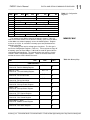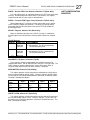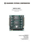
1
Series PMC521 Octal EIA/TIA-422B Communication Module USER’S MANUAL ACROMAG INCORPORATED 30765 South Wixom Road P.O. BOX 437 Wixom, MI 48393-7037 U.S.A. Copyright 2007, Acromag, Inc., Printed in the USA. Data and specifications are subject to change without notice. Tel: (248) 295-0310 Fax: (248) 624-9234 8500-756-D12D024 2 PMC521 User’s Manual EIA/TIA-422B SERIAL COMMUNICATION BOARD __________________________________________________________________ TABLE OF CONTENTS IMPORTANT SAFETY CONSIDERATIONS You must consider the possible negative effects of power, wiring, component, sensor, or software failure in the design of any type of control or monitoring system. This is very important where property loss or human life is involved. It is important that you perform satisfactory overall system design and it is agreed between you and Acromag, that this is your responsibility. 1.0 General Information The information of this manual may change without notice. Acromag makes no warranty of any kind with regard to this material, including, but not limited to, the implied warranties of merchantability and fitness for a particular purpose. Further, Acromag assumes no responsibility for any errors that may appear in this manual and makes no commitment to update, or keep current, the information contained in this manual. No part of this manual may be copied or reproduced in any form without the prior written consent of Acromag, Inc. KEY 521 FEATURES ................................................ PCI INTERFACE FEATURES ................................... SIGNAL INTERFACE PRODUCTS ........................... Board DLL Control Software ................................... Board VxWORKS Software ..................................... Board QNX Software ................................................ 4 5 5 6 6 6 2.0 PREPARATION FOR USE UNPACKING AND INSPECTION.............................. CARD CAGE CONSIDERATIONS ............................ BOARD CONFIGURATION....................................... Default Configuration ....................................... Front Panel I/O ................................................... Rear J4 Field I/O Connector ............................. Non-Isolation Considerations .......................... 7 7 7 7 8 9 9 3.0 PROGRAMMING INFORMATION PCI CONFIGURATION ADDRESS SPACE .............. PCI configuration address space..................... Configuration registers ..................................... MEMORY MAP .......................................................... Global Interrupt Status Register ...................... 8XMODE .............................................................. RESET ................................................................. Global Interrupt Enable ..................................... RHR – Receive Holding Register ..................... THR – Receive Holding Register ...................... DLL and DLM – Divisor Latch Registers ......... IER - Interrupt Enable Register ........................ ISR - Interrupt Status Register ......................... FCR – FIFO Control Register ............................ LCR – Line Control Register ............................. MCR – Modem Control Register ....................... LSR – Line Status Register ............................... MSR – Modem Status Register ......................... SCR – Scratch Pad Register ............................. FCTR – Feature Control Register ..................... EFR – Enhanced Feature Register ................... TXCNT – Transmit FIFO Level Counter ........... TXTRG – Transmit FIFO Trigger Level ............ RXCNT – Receive FIFO Level Counter ............ RXTRG – Receive FIFO Trigger Level ............. XCHAR Register ................................................ XON/XOFF – 1,2 Registers ............................... 10 10 10 11 14 14 14 14 15 15 15 16 17 19 20 21 22 23 24 24 25 26 26 27 27 27 27 _________________________________________________________________________________________ Acromag, Inc. Tel:248-295-0310 Fax:248-624-9234 Email:[email protected] http://www.acromag.com PMC521 User’s Manual EIA/TIA-422B SERIAL COMMUNICATION BOARD ___________________________________________________________________ Read RX FIFO Register ...................................... Write TX FIFO Register ...................................... Read RX FIFO with Errors Register.................. THE EFFECT OF RESET .......................................... PMC521 PROGRAMMING CONSIDERATIONS....... FIFO Polled Mode ............................................... FIFO Interrupt Mode ........................................... Loopback Mode Operation ................................ Software Flow Control ....................................... Hardware Flow Control ...................................... Programming Example ...................................... 27 27 28 28 29 29 29 30 30 31 32 3 TABLE OF CONTENTS 4.0 THEORY OF OPERATION EIA/TIA-422B SERIAL INTERFACE ......................... PMC521 OPERATION ............................................... LOGIC/POWER INTERFACE .................................... 33 34 35 5.0 SERVICE AND REPAIR SERVICE AND REPAIR ASSISTANCE .................... PRELIMINARY SERVICE PROCEDURE .................. WHERE TO GET HELP ............................................. 36 36 36 6.0 SPECIFICATIONS PHYSICAL.................................................................. ENVIRONMENTAL .................................................... UART .......................................................................... RS-422/485 CHANNELS ........................................... RS-422/485 TRANSMITTER OUTPUTS ................... RS-422/485 RECEIVER INPUTS ............................... PCI LOCAL BUS INTERFACE .................................. 37 37 38 38 38 38 38 APPENDIX CABLE: MODEL 5028-432 ........................................ TERMINATION PANEL: MODEL 5025-288 .............. 40 40 DRAWINGS 4502-021 PMC521 BLOCK DIAGRAM……………… 4502-020 PMC521 INTERFACE DIAGRAM………... 4502-019 PMC521 RESISTOR LOCATIONS….…… 4501-919 CABLE 5028-432 (SHIELDED) ................. 4501-920 TERMINATION PANEL 5025-288 ............. 41 42 43 44 44 Trademarks are the property of their respective owners. RELATED PUBLICATIONS The following datasheet provides additional information for in depth understanding of the PMC521. XR17D158 Datasheet http://www.exar.com _________________________________________________________________________________________ Acromag, Inc. Tel:248-295-0310 Fax:248-624-9234 Email:[email protected] http://www.acromag.com 4 PMC521 User’s Manual EIA/TIA-422B SERIAL COMMUNICATION BOARD __________________________________________________________________ 1.0 GENERAL INFORMATION The PMC521 board provides eight EIA/TIA-422B serial communication channels from a single PMC socket. The EIA/TIA-485 standard is also supported. The transmit and receive paths of each channel include generous 64byte FIFO buffers to minimize CPU interaction. Character size, stop bits, parity, and baud rate are software configurable. Prioritized interrupt generation is also supported for transmit, receive, line status, and data set conditions. The PMC521 utilizes state of the art Surface-Mounted Technology (SMT) to achieve its wide functionality and is an ideal choice for a wide range of industrial communication interface applications that require a highly reliable, high-performance interface at a low cost. Table 1.1: The PMC521 boards are available in standard and extended temperature ranges KEY PMC521 FEATURES MODEL Board Form Factor PCI Mezzanine Card PCI Mezzanine PMC521R Card (Rear I/O) PCI Mezzanine PMC521E Card PCI Mezzanine PMC521RE Card (Rear I/O) PMC521 Description Eight EIA/TIA-422B Channels Eight EIA/TIA-422B Channels Eight EIA/TIA-422B Channels Eight EIA/TIA-422B Channels OPERATING TEMPERATURE RANGE 0°C to +70°C 0°C to +70°C -40°C to +85°C -40°C to +85°C • High density – Provides programmable control of eight EIA/TIA-422B serial channels. • 64-Character FIFO Buffers - Both the transmit and receive channels of each serial port provide 64-byte data buffering to reduce CPU interactions and interrupts. This allows the external processor to handle more tasks within a given time. • Programmable Character Size - Each serial port is software programmable for 5, 6, 7, or 8 bit character sizes. • Programmable Stop Bits - Each serial port allows 1, 1-1/2, or 2 stopbits to be added to, or deleted from, the serial data stream. • Programmable Parity Generation & Detection - Even, Odd, or No Parity generation and detection is supported. • Line-Break Generation & Detection - provision for sending and detecting the line break character is provided. • False Start Bit Detection - Prevents the receiver from assembling false data characters due to low-going noise spikes on the RX input line. • Programmable Baud Rate - The internal baud rate generator allows a 16 921.6K baud rate to be divided by any divisor between 1 and (2 – 1), providing support for all standard baud rates. Note an additional multiplication factor of two is available resulting in a 1.8432M maximum baud rate using the standard crystal. Baud rates up to 3.125Mbps are available with a user-specified crystal. • Interrupt Support - Individually controlled transmit empty, receive ready, line status, data set, & flow control interrupts may be generated. _________________________________________________________________________________________ Acromag, Inc. Tel:248-295-0310 Fax:248-624-9234 Email:[email protected] http://www.acromag.com PMC521 User’s Manual EIA/TIA-422B SERIAL COMMUNICATION BOARD ___________________________________________________________________ • Internal Diagnostic Capabilities - Loopback controls for communication link fault isolation are included. Break, parity, overrun, and framing error simulation are also possible. • Compatible with Industry Standard UARTs - Each UART of this PMC module has its own 16550 UART compatible configuration register set. • Software Flow Control - One or two sequential receive data characters are compared to a programmed Xon or Xoff character value. Data transmission can be suspended or resumed via software flow control. • Hardware (CTS) Flow Control - The CTS signal is monitored for remote buffer overflow indication and will suspend transmissions if it becomes active. • High density – Single-width PMC Target module. • Field Connections – All eight EIA/TIA-422B serial channels connections are made through a single 68-pin SCSI front panel I/O connector. Models PMC521R and PMC521RE, only use J4 - 64 pin rear I/O connector. • 32, 16, 8-bit I/O - Register Read/Write is performed through data transfer cycles in the PCI memory space. All registers can be accessed via 32, 16, or 8-bit data transfers. • Compatibility – Complies to PCI Local Bus Specification Revision 2.3. Provides one multifunction interrupt. . Universal PCI Bus buffers – Auto sense 3.3V or 5V operation. Cables and a termination panel are also available to interface with this board, via the 68 pin SCSI front panel connector. Cable: Model 5028-432: A 2-meter, round 68 conductor shielded cable with a male SCSI-3 connector at both ends and 34 twisted pairs. The cable is used for connecting the board to Model 5025-288 termination panels. For optimum performance, use the shortest possible length of shielded input cable. 5 KEY PMC521 FEATURES PCI INTERFACE FEATURES SIGNAL INTERFACE PRODUCTS See the Appendix for further information on these products. Termination Panel: Model 5025-288: DIN-rail mountable panel provides 68 screw terminals for universal field I/O termination. Connects to Acromag board, via SCSI-3 to twisted pair cable described above. _________________________________________________________________________________________ Acromag, Inc. Tel:248-295-0310 Fax:248-624-9234 Email:[email protected] http://www.acromag.com 6 PMC521 User’s Manual EIA/TIA-422B SERIAL COMMUNICATION BOARD __________________________________________________________________ BOARD DLL CONTROL SOFTWARE BOARD VxWORKS SOFTWARE BOARD QNX SOFTWARE Acromag provides a software product (sold separately) to facilitate the development of Windows (98/Me/2000/XP) applications accessing Acromag PMC I/O board products, PCI I/O Cards, and CompactPCI I/O Cards. This software (Model PCISW-API-WIN) consists of low-level drivers and Windows 32 Dynamic Link Libraries (DLLs) that are compatible with a number of programming environments including Visual C++, Visual Basic, Borland C++ Builder and others. The DLL functions provide a high-level interface to boards eliminating the need to perform low-level reads/writes of registers, and the writing of interrupt handlers. Acromag provides a software product (sold separately) consisting of board VxWorks software. This software (Model PMCSW-API-VXW) is composed of VxWorks (real time operating system) libraries for all Acromag PMC I/O board products, PCI I/O Cards, and CompactPCI I/O Cards. The software is implemented as a library of “C” functions which link with existing user code to make possible simple control of all Acromag PMC boards. Acromag provides a software product (sold separately) consisting of board QNX software. This software (Model PCISW-API-QNX) is composed of QNX (real time operating system) libraries for all Acromag PMC I/O board products, PCI I/O Cards, and CompactPCI I/O Cards. The software is implemented as a library of “C” functions which link with existing user code to make possible simple control of all Acromag PMC boards. _________________________________________________________________________________________ Acromag, Inc. Tel:248-295-0310 Fax:248-624-9234 Email:[email protected] http://www.acromag.com PMC521 User’s Manual EIA/TIA-422B SERIAL COMMUNICATION BOARD ___________________________________________________________________ Upon receipt of this product, inspect the shipping carton for evidence of mishandling during transit. If the shipping carton is badly damaged or water stained, request that the carrier's agent be present when the carton is opened. If the carrier's agent is absent when the carton is opened and the contents of the carton are damaged, keep the carton and packing material for the agent's inspection. 7 2.0 PREPARATION FOR USE UNPACKING AND INSPECTION For repairs to a product damaged in shipment, refer to the Acromag Service Policy to obtain return instructions. It is suggested that salvageable shipping cartons and packing material be saved for future use in the event the product must be shipped. This board is physically protected with packing material and electrically protected with an anti-static bag during shipment. However, it is recommended that the board be visually inspected for evidence of mishandling prior to applying power. Refer to the specifications for loading and power requirements. Be sure that the system power supplies are able to accommodate the power requirements of the carrier/CPU board, plus the installed boards, within the voltage tolerances specified. Adequate air circulation must be provided to prevent a temperature rise above the maximum operating temperature and to prolong the life of the electronics. If the installation is in an industrial environment and the board is exposed to environmental air, careful consideration should be given to airfiltering. Remove power from the system before installing board, cables, termination panels, and field wiring. The board may be configured differently, depending on the application. When the board is shipped from the factory, it is configured as follows: • The default configuration of the programmable software control register bits at power-up are described in section 3. • The control registers must be programmed to the desired configuration before starting data input or output operation. WARNING: This board utilizes static sensitive components and should only be handled at a staticsafe workstation. CARD CAGE CONSIDERATIONS IMPORTANT: Adequate air circulation must be provided to prevent a temperature rise above the maximum operating temperature. BOARD CONFIGURATION Default Configuration _________________________________________________________________________________________ Acromag, Inc. Tel:248-295-0310 Fax:248-624-9234 Email:[email protected] http://www.acromag.com 8 PMC521 User’s Manual EIA/TIA-422B SERIAL COMMUNICATION BOARD __________________________________________________________________ Front Panel Field I/O Connector The front panel connector provides the field I/O interface connections. It is a SCSI-3 68-pin female connector (AMP 787082-7 or equivalent) employing latch blocks and 30 micron gold in the mating area (per MIL-G45214, Type II, Grade C). Connects to Acromag termination panel 5025288 from the front panel via round shielded cable (Model 5028-432). All eight EIA/TIA-422B serial communication channels for interfacing are shown in table 2.1. Each channel has eight signals and are designated by channels 0 through channel 7. Table 2.1: Board Field I/O Pin Connections The board has eight EIA/TIA422B serial communication channels. Pin Description TX0+ TX0RX0+ RX0RTS0+ RTS0CTS0+ CTS0TX1+ TX1RX1+ RX1RTS1+ RTS1CTS1+ CTS1TX2+ TX2RX2+ RX2RTS2+ RTS2CTS2+ CTS2TX3+ TX3RX3+ RX3RTS3+ RTS3CTS3+ CTS3COMMON COMMON Pin 1 2 3 4 5 6 7 8 9 10 11 12 13 14 15 16 17 18 19 20 21 22 23 24 25 26 27 28 29 30 31 32 33 34 Pin Description TX4+ TX4RX4+ RX4RTS4+ RTS4CTS4+ CTS4TX5+ TX5RX5+ RX5RTS5+ RTS5CTS5+ CTS5TX6+ TX6RX6+ RX6RTS6+ RTS6CTS6+ CTS6TX7+ TX7RX7+ RX7RTS7+ RTS7CTS7+ CTS7COMMON COMMON Pin 35 36 37 38 39 40 41 42 43 44 45 46 47 48 49 50 51 52 53 54 55 56 57 58 59 60 61 62 63 64 65 66 67 68 _________________________________________________________________________________________ Acromag, Inc. Tel:248-295-0310 Fax:248-624-9234 Email:[email protected] http://www.acromag.com PMC521 User’s Manual EIA/TIA-422B SERIAL COMMUNICATION BOARD ___________________________________________________________________ On models with rear I/O, the J4 PMC connector provides the field I/O interface connections. This connector is a 64-pin female receptacle header (AMP 120527-1 or equivalent) which mates to the male connector on the carrier/CPU board (AMP 120521-1 or equivalent). 9 Rear J4 Field I/O Connector All eight EIA/TIA-422B serial communication channels for interfacing are shown in table 2.2. Each channel has eight signals and are designated by channels 0 through channel 7. Pin Description Pin Pin Description Pin TX0+ TX4+ 1 33 TX0TX42 34 RX0+ RX4+ 3 35 RX0RX44 36 RTS0+ RTS4+ 5 37 RTS0RTS46 38 CTS0+ CTS4+ 7 39 CTS0CTS48 40 TX1+ TX5+ 9 41 TX1TX510 42 RX1+ RX5+ 43 11 RX1RX512 44 RTS1+ RTS5+ 13 45 RTS1RTS514 46 CTS1+ CTS5+ 15 47 CTS1CTS516 48 TX2+ TX6+ 17 49 TX2TX618 50 RX2+ RX6+ 19 51 RX2RX620 52 RTS2+ RTS6+ 21 53 RTS2RTS622 54 CTS2+ CTS6+ 23 55 CTS2CTS624 56 TX3+ TX7+ * 25 57 TX3TX726 58 RX3+ RX7+ 27 59 RX3RX728 60 RTS3+ CTS7+ 29 61 RTS3CTS7 30 62 CTS3+ COMMON 31 63 CTS3COMMON 32 64 * Note: Channel 7 does not use RTS7+ or RTS7- signals due to not enough I/O pins on Rear I/O connector. These signals are used on Front I/O models only. The board is non-isolated, since there is electrical continuity between the logic and field I/O grounds. As such, the field I/O connections are not isolated from the system. Care should be taken in designing installations without isolation to avoid noise pickup and ground loops caused by multiple ground connections. This is particularly important for analog inputs and outputs when a high level of accuracy/resolution is needed. Table 2.2: Board Rear Field I/O Pin Connections The board has eight EIA/TIA422B serial communication channels. Non-Isolation Considerations _________________________________________________________________________________________ Acromag, Inc. Tel:248-295-0310 Fax:248-624-9234 Email:[email protected] http://www.acromag.com 10 PMC521 User’s Manual EIA/TIA-422B SERIAL COMMUNICATION BOARD __________________________________________________________________ 3.0 PROGRAMMING INFORMATION This Section provides the specific information necessary to program and operate the board. This board is a PCI Specification version 2.3 compliant PCI bus target only board. The PCI bus is defined to address three distinct address spaces: I/O, memory, and configuration space. This board can be accessed via the PCI bus memory space and configuration spaces, only. The card’s configuration registers are initialized by system software at power-up to configure the card. The board is a Plug-and-Play PCI card. As a Plug-and-Play card the board’s base address and system interrupt request line are not selected via jumpers but are assigned by system software upon power-up via the configuration registers. A PCI bus configuration access is used to read/write the PCI card’s configuration registers. PCI Configuration Address Space When the computer is first powered-up, the computer’s system configuration software scans the PCI bus to determine what PCI devices are present. The software also determines the configuration requirements of the PCI card. The system software accesses the configuration registers to determine how many blocks of memory space the carrier requires. It then programs the board’s configuration registers with the unique memory base address. The configuration registers are also used to indicate that the board requires an interrupt request line. The system software then programs the configuration registers with the interrupt request line assigned to the board. Since this board is relocatable and not fixed in address space, its device driver must use the mapping information stored in the board’s Configuration Space registers to determine where the board is mapped in memory space and which interrupt line will be used. PCI CONFIGURATION REGISTERS The PCI specification requires software driven initialization and configuration via the Configuration Address space. This board provides 256 bytes of configuration registers for this purpose. It contains the configuration registers, shown in Table 3.1, to facilitate Plug-and-Play compatibility. The Configuration Registers are accessed via the Configuration Address and Data Channels. The most important Configuration Registers are the Base Address Registers and the Interrupt Line Register which must be read to determine the base address assigned to the board and the interrupt request line that goes active on a board interrupt request. _________________________________________________________________________________________ Acromag, Inc. Tel:248-295-0310 Fax:248-624-9234 Email:[email protected] http://www.acromag.com PMC521 User’s Manual EIA/TIA-422B SERIAL COMMUNICATION BOARD ___________________________________________________________________ Reg. Num. 0 1 2 3 4 5 : 10 11 12 13,14 15 D31 D24 D23 D16 D15 D8 D7 D0 11 Table 3.1 Configuration Registers Device ID=0521 Vendor ID= 16D5 Status Command Class Code=070002 Rev ID=02 BIST Header Latency Cache 32-bit Memory Base Address for 4K-Byte Block Not Used Subsystem ID=0521 Subsystem Vendor ID=16D5 Not Used Reserved Max_Lat Min_Gnt Inter. Pin Inter. Line The memory space address map for the board is shown in Table 3.2. Note that the base address for the board in memory space must be added to the addresses shown to properly access the board registers. Register accesses as 32, 24, 16, and 8-bit in memory space are permitted unless otherwise specified. The memory space consists of two types of registers. The first type is the Device Configuration Registers (Table 3.3). These registers occupy 4K of memory space at Base Address + 80H and are used for general device configuration and monitoring. The second register type consists of each channel’s UART configuration registers. These are used to control and monitor the status of the individual channels. D07 D00 LCR Base Addr+ MEMORY MAP Table 3.2: Memory Map UART Channel 0 READ – RHR Channel 0 - Receive Holding Register Bit 7= 0 00 WRITE – THR Channel 0 - Transmit Holding Register Bit 7 = 0 00 READ/WRITE – DLL Channel 0 - Divisor Latch Low Bit 7 = 1 00 READ/WRITE – DLM Channel 0 - Divisor Latch High Bit 7 = 1 01 READ/WRITE – IER Channel 0 - Interrupt Enable Register 01 READ – ISR Channel 0 - Interrupt Status Register 02 WRITE – FCR Channel 0 - FIFO Control Register 02 READ/WRITE – LCR Channel 0 - Line Control Register 03 READ/WRITE – MCR Channel 0 - Modem Control Register 04 READ – LSR Channel 0 - Line Status Register 05 _________________________________________________________________________________________ Acromag, Inc. Tel:248-295-0310 Fax:248-624-9234 Email:[email protected] http://www.acromag.com 12 PMC521 User’s Manual EIA/TIA-422B SERIAL COMMUNICATION BOARD __________________________________________________________________ MEMORY MAP D07 D00 Comments READ – MSR Channel 0 - Modem Status Register WRITE – RS485 Channel 0 - Turn-Around Delay Register Base Addr+ 06 Not Supported 06 READ/WRITE – SPR Channel 0 - Scratch Pad Register 07 READ/WRITE – FCTR Channel 0 – Feature Control Register 08 READ/WRITE – EFR Channel 0 – Enhanced Function Register 09 READ – TXCNT Channel 0 – Transmit FIFO Level Counter 0A WRITE – TXTRG Channel 0 – Transmit FIFO Trigger Level 0A READ – RXCNT Channel 0 – Receive FIFO Level Counter 0B WRITE – RXTRG Channel 0 – Receive FIFO Trigger Level 0B WRITE Channel 0 – Xoff-1 – Xoff Character 1 0C READ Channel 0 – Xchar Xon, Xoff Rcvd. Flags 0C WRITE Channel 0 – Xoff-2 – Xoff Character 2 0D WRITE Channel 0 – Xon-1 – Xon Character 1 0E WRITE Channel 0 – Xon-2 – Xon Character 2 0F Reserved 10-7F DEVICE CONFIGURATION REGISTERS See Table 3.3 80-93 94-FF Reserved READ Channel 0 – Read FIFO Data Width 8/16/24/32 100-13F WRITE Channel 0 – Write FIFO Data Width 8/16/24/32 100-13F 140-17F Reserved READ Channel 0 – Read FIFO with errors Data Width 16/32 180-1FF UART Channel 1 Channel 1 – Registers 200-20F Reserved 210-2FF READ Channel 1 – Read FIFO Data Width 8/16/24/32 300-33F _________________________________________________________________________________________ Acromag, Inc. Tel:248-295-0310 Fax:248-624-9234 Email:[email protected] http://www.acromag.com PMC521 User’s Manual EIA/TIA-422B SERIAL COMMUNICATION BOARD ___________________________________________________________________ D07 D00 Comments Base Addr+ Data Width 8/16/24/32 300-33F WRITE Channel 1 – Write FIFO 13 MEMORY MAP 340-37F Reserved READ Channel 1 – Read FIFO with errors Data Width 16/32 380-3FF UART Channel 2 400-5FF UART Channel 3 600-7FF UART Channel 4 800-9FF UART Channel 5 A00-BFF UART Channel 6 C00-DFF UART Channel 7 E00-FFF Notes (Table 3.2): 1. To save user manual space the registers corresponding to channels 1 to 7 have not been individually shown. The registers of channels 1 to 7 are in the address space shown above. To access a register in channel 7, for example, the offset of E00 hex is added to the address of the corresponding register given in table 3.2. All channels require a 512 byte memory block. REGISTER Byte 3 [31:24] Byte 2 [23:16] Byte 1 [15:8] Byte 0 [7:0] Base Addr+ Global Interrupt Status (Read-only) Timer (Read/Write) INT3 INT2 INT1 INT0 80-83 TIMER MSB TIMER LSB TIMER (reserved) TIMER CNTL 84-87 Ancillary1 (Read/Write) SLEEP RESET REGA (reserved) 8XMODE 88-8B Ancillary2 (Read-only) MPIOINT REGB DVID DREV 8C-8F MPIO (Read/Write) MPIOSEL MPIOINV MPIO3T MPIOLVL 90-93 Table 3.3: Device Configuration Registers shown in DWORD alignment. This memory map reflects byte accesses using the “Little Endian” byte ordering format. Little Endian uses even-byte addresses to store the loworder byte. The Intel x86 family of microprocessors uses “Little Endian” byte ordering. Big Endian is the convention used in the Motorola 68000 microprocessor family and is the VMEbus convention. In Big Endian, the lower-order byte is stored at odd-byte addresses. This board operates in two different modes. In one mode, this device remains software compatible with the industry standard 16C550 family of UART’s and provides double-buffering of data registers. In the FIFO Mode (enabled via bit 0 of the FCR register), data registers are FIFO-buffered so that read and write operations can be performed while the UART is performing serial-to-parallel and parallel-to-serial conversions. Two FIFO modes are possible: FIFO Interrupt Mode and FIFO Polled Mode. Some registers operate differently between the available modes and this is noted in the following paragraphs. _________________________________________________________________________________________ Acromag, Inc. Tel:248-295-0310 Fax:248-624-9234 Email:[email protected] http://www.acromag.com 14 PMC521 User’s Manual EIA/TIA-422B SERIAL COMMUNICATION BOARD __________________________________________________________________ DEVICE CONFIGURATION REGISTERS Note: Only device configuration registers that are supported by the PMC521 are described in this section. Global Interrupt Status Register (READ Only) This 32-bit wide register [INT0, INT1, INT2 and INT3] provides interrupt source and type information. Each of the first 8 bits (INT0) represents a channel and indicates if that channel has requested service. For example INT0 bit-0 represents the interrupt status for channel 0 and INT0 bit-7 represents the interrupt status for channel 7. An interrupt service routine can inspect INT0 to determine that a channel requires service and then read the channel’s Interrupt Status Register (ISR) to determine the source of the interrupt. INT3, INT2 and INT1 [31:8] provide a twenty-four bit encoded interrupt indicator. Each channel’s interrupt is encoded into 3 bits for receive, transmit and status. Bits [10:8] represent channel 0, bits [13:11] represent channel 1 and so forth. The table below shows the 3 bit encoding and priority order. This interrupt source encoding provides much of the same interrupt source data that would be obtained by reading each channel’s ISR. Interrupt clearing is covered in the description of the Interrupt Status Register UART Channel [7:0] Interrupt Source Encoding Priority Bit[N + 2] Bit[N + 1] Bit[N + 0] Source of the Interrupt x 0 0 0 None 1 0 0 1 RXRDY and RX Line Status 2 0 1 0 RXRDY Timeout 3 0 1 1 TXRDY or THR empty 4 1 1 0 MSR, RTS/CTS or DTR/DSR delta or Xoff/Xon detected or special character detected 8XMODE (Read/Write) Each bit of this 8-bit register selects an 8X or 16X sampling rate for the corresponding UART channel. Channels 7 to 0 are configured using bits 7 to 0 respectively. Logic 0 (default) selects normal 16X sampling while logic 1 selects 8X sampling rate. Transmit and receive data rates will double by selecting 8X. RESET (Read/Write) UART channels 7 to 0 can be reset using bits 7 to 0 respectively. After setting a bit to logic 1, all registers in the corresponding channel will be reset to the default condition. Each bit is self-resetting after it is written. Global Interrupt Enable (Read/Write) On the PMC521 the UART’s multi-purpose input/output 0 (MPIO0) is used internally as a Global Interrupt Enable switch. In order for any UART channel interrupts to be seen by the system, the multi-purpose input/output registers must be configured as follows: 1. The MPIOINT, MPIO3T, and MPI03T registers should be left in their default states (all bits low). 2. The MPIOSEL register should be set to FEH (FFH is the default). This configures MPIO pin 0 as an output. 3. MPIOLVL bits 7 to 1 should be left in their default state (low). 4. MPIOLVL bit 0 now acts as the Global Interrupt Enable bit. 0 = Disable Interrupt 1 = Enable Interrupt _________________________________________________________________________________________ Acromag, Inc. Tel:248-295-0310 Fax:248-624-9234 Email:[email protected] http://www.acromag.com PMC521 User’s Manual EIA/TIA-422B SERIAL COMMUNICATION BOARD ___________________________________________________________________ RHR - Receive Holding Register, Channels 0-7 (READ Only) The Receive Holding Register (RHR) is a serial channel input data register that receives the input data from the receiver shift register. Note that the RHR will only receive data if the transceiver is first enabled to receive data. The transceiver is enabled to receive data by setting bit-0 of the MCR (Modem Control Register) to logic 1. 15 UART CONFIGURATION REGISTERS The RHR holds from 5 to 8 bits of data, as specified by the character size programmed in the Line Control Register (LCR bits 0 and 1). If less than 8 bits are transmitted, then data is right-justified to the LSB. If parity is used, then LCR bit 3 (parity enable) and LCR bit 4 (type of parity) are required. Status for the receiver is provided via the Line-Status Register (LSR). When a full character is received (including parity and stop bits), the data-received indication bit (bit 0) of the LSR is set to 1. The host CPU then reads the Receiver Buffer Register, which resets LSR bit 0 low. If the character is not read prior to a new character transfer between the receiver shift register and the receive holding register, the overrun-error status indication is set in LSR bit 1. If there is a parity error, the error is indicated in LSR bit 2. If a stop bit is not detected, a framing error indication is set in bit 3 of the LSR. Serial asynchronous data is input to the receiver shift register via the receive data line. From the idle state, this line is monitored for a high-to-low transition (start bit). When the start bit is detected, an internal receiver counter starts counting at the 16x or 8x clock rate. After 8 or 4 clocks the start bit period should be at its center. The start bit is judged valid if it is still low at this point. This is known as false start-bit detection. By verifying the start bit in this manner, it helps to prevent the receiver from assembling an invalid data character due to a low-going noise spike on the receive data line. THR - Transmit Holding Register, Channels 0-7 (WRITE Only) The Transmitter Holding Register (THR) is a serial channel output data register that shifts the data to the transmit data line (TX). However, the THR data will not pass to the TX line unless the transceiver is first enabled. The transceiver must be enabled to transmit data by setting bit-1 of the MCR (Modem Control Register) to logic 1. The THR holds from 5 to 8 bits of data, as specified by the character size programmed in the Line Control Register. If less than 8 bits are transmitted, then data is entered right-justified to the LSB. This data is framed as required, then shifted to the transmit data line. The THR is also the input register to the transmit FIFO when FIFO operation is enabled by FCR bit-0. The status of the THR is provided in the Line Status Register (LSR). The THR empty flag in the LSR register is set to a logic 1 when the last data byte is transferred from the THR to the transmit shift register. DLL & DLM - Divisor Latch Registers, Channels 0-7 (R/W) Each channel has its own Baud Rate Generator (BRG) with a prescaler for the transmitter and receiver. A software bit in the Modem Control Register (MCR) controls the prescaler. The MCR register bit-7 sets the prescaler to divide the 14.7456MHz crystal by 1 or 4. The output of the prescaler clocks to the BRG. The BRG(16-1) further divides this clock by a programmable divisor between 1 and 2 to obtain a 16x or 8x sampling clock of the serial data rate. Two 8-bit divisor latch registers per channel are used to store the divisors in 16-bit binary format. The DLL register stores the low-order byte of the divisor and DLM stores the high-order byte. These registers default to random values during upon power up and must be loaded during initialization. _________________________________________________________________________________________ Acromag, Inc. Tel:248-295-0310 Fax:248-624-9234 Email:[email protected] http://www.acromag.com 16 PMC521 User’s Manual EIA/TIA-422B SERIAL COMMUNICATION BOARD __________________________________________________________________ UART CONFIGURATION REGISTERS Note that bit 7 of the LCR register must first be set high to access the divisor latch registers (DLL and DLM) during a read/write operation. The relationship between the baud rate, prescaler, divisor, and the 14.7456MHz clock can be summarized in the following equations: Divisor = 14.7456MHz 16 × Baud Rate × Prescaler with 8XMODE = 0 Divisor = 14.7456MHz 8 × Baud Rate × Prescaler with 8XMODE = 1 The Prescaler term represents the state of MCR bit-7 as follows: Prescaler = 1 If MCR bit-7=0 Prescaler = 4 If MCR bit-7=1 The following table shows the correct divisor to use for generation of some standard baud rates (based on the 14.7456MHz clock at 16X clock rate). A different external crystal can replace the 14.7456MHz crystal on the circuit board to obtain unique clock rates. You may contact Acromag Applications Engineering to explore options in this area. Table 3.4: Baud Rate Divisors (14.74MHz Clock). Note: Setting 8XMODE=1 will multiply all baud rates in this table by a factor of two. BAUD RATE MCR MCR Bit-7=1 Bit-7=0 50 200 300 1200 600 2400 1200 4800 2400 9600 3600 14,400 4800 19,200 7200 28,800 9600 38,400 19,200 76,800 28,800 115,200 38,400 153,600 57,600 230,400 115,200 460,800 230,400 921,600 Decimal 4608 768 384 192 96 64 48 32 24 12 8 6 4 2 1 DIVISOR (N) DLM (HEX) 12 03 01 00 00 00 00 00 00 00 00 00 00 00 00 DLL (HEX) 00 00 80 C0 60 40 30 20 18 0C 08 06 04 02 01 The following table shows the correct divisor to use for generation of some standard baud rates (based on the 14.7456MHz clock at 16X clock rate). A different external crystal can replace the 14.7456MHz crystal on the circuit board to obtain unique clock rates. You may contact Acromag Applications Engineering to explore options in this area. IER - Interrupt Enable Register, Channels 0-7 (R/W) The Interrupt Enable Register is used to independently enable/ disable the serial channel interrupt sources. Each of the eight channels have seven unique interrupt sources which are all mapped to INTA# of the PMC module. An interrupt source is disabled by setting the corresponding IER bit to logic 0, and enabled by setting the IER bit to logic 1. Note that in order for channel interrupts to be seen by the system, the multi-purpose input/output registers must be configured properly (see the Global Interrupt Enable section). _________________________________________________________________________________________ Acromag, Inc. Tel:248-295-0310 Fax:248-624-9234 Email:[email protected] http://www.acromag.com PMC521 User’s Manual EIA/TIA-422B SERIAL COMMUNICATION BOARD ___________________________________________________________________ Interrupt Enable Register IER BIT INTERRUPT ACTION 0 RHR Interrupt Enable 0 = Disable Interrupt (default) 1 = Enable Interrupt The receive data ready interrupt will be issued when RHR has a data character in the non-FIFO mode or when the receive FIFO has reached the programmed trigger level in the FIFO mode. A receive data timeout interrupt will be issued in the FIFO mode when the receive FIFO has not reached the programmed trigger level and the RX input has been idle for 4 character + 12 bit times. 1 THR Interrupt Enable 0 = Disable Interrupt (default) 1 = Enable Interrupt This interrupt is associated with bit-5 in the LSR register. An interrupt is issued whenever the THR becomes empty or when data in the FIFO falls below programmed trigger level. 2 Receive Line Status Interrupt Enable 0 = Disable Interrupt (default) 1 = Enable Interrupt Any LSR register bits 1, 2, 3 or 4 will generate an LSR immediately when a character received in the RX FIFO has an error. 3 Modem Status Interrupt Enable 0 = Disable Interrupt (default) 1 = Enable Interrupt 4 Reserved 5 Xoff Interrupt Enable (requires EFR bit-4=1) 0 = Disable the software flow control (default) 1 = Enable the software flow control 6 RTS#/DTR# Output Interrupt Enable (requires EFR bit-4=1) 0 = Disable Interrupt (default) 1 = Enable Interrupt. The UART issues an interrupt when the RTS#/DTR# pin makes a transition. The RTS# or DTR# output is selected via MCR bit-2. A DTR signal path is NOT SUPPORTED by this model. The DTR# output is used to enable the receiver of the channel RX. Although a RTS signal path is present, the RTS# output’s primary purpose is to enable the transmitter of the channel TX. Note that using RTS# for flow control may interfere with the ability of the channel to transmit data. 7 CTS# Input Interrupt Enable (requires EFR bit-4=1) 0 = Disable Interrupt (default) 1 = Enable Interrupt. The UART issues an interrupt when the CTS# pin makes a transition. A pound sign (#) is used to indicate an active-low signal on the UART pin. 17 UART CONFIGURATION REGISTERS ISR - Interrupt Status Register, Channels 0-7 (READ Only) The Interrupt Status Register is used to indicate that a prioritized interrupt is pending and the type of interrupt that is pending. The eight individual channels share the PMC module INTA# signal. Six levels of prioritized interrupts are provided to minimize software interaction. Performing a read cycle on the ISR will provide the user with the highest pending interrupt level to be serviced. No other interrupts are acknowledged until the pending interrupt is serviced. Whenever the interrupt status register is read, the interrupt status is cleared. Note, only the current pending interrupt is cleared by the read. A lower level interrupt may be seen after re-reading the interrupt status bits. _________________________________________________________________________________________ Acromag, Inc. Tel:248-295-0310 Fax:248-624-9234 Email:[email protected] http://www.acromag.com 18 PMC521 User’s Manual EIA/TIA-422B SERIAL COMMUNICATION BOARD __________________________________________________________________ UART CONFIGURATION REGISTERS The following interrupt source table shows the data values (bit 0-5) for the seven prioritized interrupt levels and the interrupt sources associated with each of these interrupt levels. Interrupt Status Register PRIORITY ISR BITS LEVEL Bit5 to Bit0 1 000110 2 3 4 000100 001100 000010 5 6 000000 010000 7 X 100000 000001 Source of the Interrupt LSR (Receiver Line Status Register, see LSR bits 1-4) RXRDY (Received Data Ready) RXRDY (Receive Data Time-out) TXRDY (Transmitter Holding Register Empty) MSR (Modem Status Register) RXRDY (Received Xon/Xoff or Special character) CTS#, RTS#/DTR# change of state None (default) Notes (Interrupt Status Register): 1. Bit 4 of the EFR (Enhanced Feature Register) must be set to a logic 1 to unlock access to bits 4 and 5 of the ISR register. Note that ISR bit 0 can be used to indicate whether an interrupt is pending (bit 0 is low when interrupt is pending). ISR bits 1, 2, and 3 are used to indicate the source for a pending interrupt at interrupt priority levels 1, 2, 3, and 4. Bit 4 set indicates a Xoff/Xon or special character detected interrupt pending. Reading the XCHAR register will indicate which character (Xoff or Xon) was received last. Bit 5 indicates a pending interrupt due to a change of state on the CTS#/ or RTS#/DTR# signals. Bits 6 and 7 are set to a logic 0 when the FIFOs are disabled. They are set to a logic 1 when the FIFOs are enabled. Interrupt Clearing: • LSR interrupt is cleared by a read of the LSR register • RXRDY is cleared by reading data until FIFO falls below the trigger level. • RXRDY Time-out is cleared by reading data until the RX FIFO is empty. • TXRDY interrupt is cleared by a read of the ISR register. • MSR interrupt is cleared by a read of the MSR register • Xon or Xoff character interrupt is cleared by a read of the ISR register. • Special character interrupt is cleared by a read of the ISR register or after the next character is received. • RTS#/DTR# and CTS# status change interrupts are cleared by a read to the MSR register. _________________________________________________________________________________________ Acromag, Inc. Tel:248-295-0310 Fax:248-624-9234 Email:[email protected] http://www.acromag.com PMC521 User’s Manual EIA/TIA-422B SERIAL COMMUNICATION BOARD ___________________________________________________________________ FCR - FIFO Control Register, Channels 0-7 (WRITE Only) This write-only register is used to enable and clear the FIFO buffers, and set the transmit/receive FIFO trigger levels. 19 UART CONFIGURATION REGISTERS FIFO Control Register FCR BIT FUNCTION 0 TX and RX FIFO Enable 0 = Disable the transmit and receive FIFO (default). 1 = Enables both the Tx and Rx FIFO’s. This bit must be a “1” when other FCR bits are written to or they will not be programmed. 1 RX FIFO Reset This bit is only active when FCR bit-0 is active. 0 = No receive FIFO reset (default). 1 = Reset the receive FIFO pointers and FIFO level counter logic (the receive shift register is not cleared or altered). This bit will return to logic 0 after resetting the FIFO. 2 TX FIFO Reset This bit is only active when FCR bit-0 is active. 0 = No transmit FIFO reset (default). 1 = Reset the transmit FIFO pointers and FIFO level counter logic (the transmit shift register is not cleared or altered). This bit will return to logic 0 after resetting the FIFO. 3 DMA Mode Select (DMA Not Supported) 1 Transmit FIFO Trigger Select 5,4 These bits are used to set the trigger level for the transmit FIFO interrupt. An interrupt will be issued when the number of characters in the FIFO drops below the selected trigger level, or when the FIFO becomes empty in the case that it did not get filled over the trigger level on last reload.2 FCTR bits 6-7 are used to select one of four trigger tables . Table Bit 5 Bit 4 Trigger Level A 0 0 1 (default) B 0 0 1 1 0 0 1 1 X 0 1 0 1 0 1 0 1 X 16 8 24 30 8 16 32 56 Programmable C D _________________________________________________________________________________________ Acromag, Inc. Tel:248-295-0310 Fax:248-624-9234 Email:[email protected] http://www.acromag.com 20 PMC521 User’s Manual EIA/TIA-422B SERIAL COMMUNICATION BOARD __________________________________________________________________ UART CONFIGURATION REGISTERS FCR BIT 7,6 FUNCTION Receive FIFO Trigger Select These bits are used to set the trigger level for the receiver FIFO interrupt. In FIFO mode an interrupt is generated when the number of characters in the FIFO equals the programmed trigger level. FCTR bits 6-7 are used to select 2 one of four trigger tables . Table Bit 7 Bit 6 Trigger Level A 0 0 1 (default) 0 1 4 1 0 8 1 1 14 B 0 0 8 0 1 16 1 0 24 1 1 28 C 0 0 8 0 1 16 1 0 56 1 1 60 D X X Programmable Notes (FIFO Control Register): 1. Bits 4 and 5 are only programmable when the EFR bit 4 is set to 1. 2. The receiver and transmitter cannot use different trigger tables. The table selected last applies to both the RX and TX side. LCR - Line Control Register, Channels 0-7 (Read/Write) The Line Control Register is used to specify the asynchronous data communication format. The word length, the number of stop bits, and the parity are selected by writing the appropriate bits in this register. Line Control Register LCR Bit FUNCTION 1,0 Word Length Sel. 2 Stop Bit Select 3 Parity Enable 4 Parity Select Forced Parity Select 5 6 Transmit Break Enable PROGRAMMING 0 0 = 5 Data Bits (default) 0 1 = 6 Data Bits 1 0 = 7 Data Bits 1 1 = 8 Data Bits 0 = 1 Stop Bit (default) 1 = 1.5 Stop Bits if 5 data bits; 2 Stop Bits if 6, 7, or 8 data bits selected. 0 = No Parity 1 = A parity bit is generated during the transmission while the receiver checks for parity error of the data character received. 0 = ODD Parity 1 = EVEN Parity 0 = parity is not forced (default) 1 and LCR BIT-4 = 0, parity bit is forced to a logic 1 (MARK) for the transmit and received data. 1 and LCR BIT-4 = 1, parity bit is forced to a logic 0 (SPACE) for the transmit and received data. 0 = No TX break condition (default) 1 = Forces the transmitter output (TX) to a “space”, LOW, for alerting the remote receiver of a line break condition. This condition remains until disabled by setting LCR bit-6 to a logic 0. _________________________________________________________________________________________ Acromag, Inc. Tel:248-295-0310 Fax:248-624-9234 Email:[email protected] http://www.acromag.com PMC521 User’s Manual EIA/TIA-422B SERIAL COMMUNICATION BOARD ___________________________________________________________________ LCR Bit 7 FUNCTION Baud Rate Divisor (DLL/DLM) Enable PROGRAMMING 0 = Data registers are selected (default). 1 = Divisor latch registers are selected. 21 UART CONFIGURATION REGISTERS A detailed discussion of word length, stop bits, parity, and the break signal is included in Section 4.0 (Theory of Operation). MCR - Modem Control Register, Channels 0-7 (R/W) The Modem Control register is used for controlling the modem interface signals or general purpose inputs/outputs. Modem Control Register MCR Bit FUNCTION 0 DTR# Pins 1 RTS# Pins 2 Auto Flow Control Select 3 4 (OP2) Internal 1 Loopback Enable Xon-Any Enable 2 5 6 2 7 Infrared Encoder/ Decoder Enable Clock Prescaler Select PROGRAMMING 0 = Channel receiver disabled 1 = Channel receiver enabled A DTR signal path is NOT SUPPORTED by this model. Instead, the output is used to enable the receiver of the channel RX. 0 = Channel transmitter disabled 1 = Channel transmitter enabled Although a RTS signal path is present, the RTS# output’s primary purpose is to enable the transmitter of the channel TX. Note that using RTS# for flow control may interfere with the ability of the channel to transmit data. The UART uses this bit to select between RTS/CTS (bit-2 = 0) or DTR/DSR (bit-2 = 1) for auto hardware flow control. Since this DTR and DSR signal paths are not supported this bit should be left at logic 0 (default). This bit is only in effect when auto RTS/DTR is enabled by EFR bit-6 OP2 is not available 0 = Disabled internal loopback mode (default) 1 = Enabled internal loopback mode 0 = Disable Xon-Any function (default) 1 = Enable any Xon-any function. In this mode any RX character received will enable Xon, resume data transmission. Infrared mode is not supported 0 = Divide by one. The input clock from the crystal is fed directly to the Programmable Baud Rate Generator without further modifications, i.e., divide by one (default) 1 = Divide by four. The prescaler divides the input clock from the crystal by four and feeds it to the Programmable Baud Rate Generator, hence, data rates become one-forth. _________________________________________________________________________________________ Acromag, Inc. Tel:248-295-0310 Fax:248-624-9234 Email:[email protected] http://www.acromag.com 22 PMC521 User’s Manual EIA/TIA-422B SERIAL COMMUNICATION BOARD __________________________________________________________________ UART CONFIGURATION REGISTERS Notes (Modem Control Register): MCR Bit 4 provides a local loopback feature for diagnostic testing of the UART channel. All UART functions operate normally. Transmit data from the transmit shift register is internally routed to the receive shift register input allowing the system to receive the same data that it was sending. The TX, RTS# and DTR# pins are held de-asserted, and the CTS# input is ignored. 2. Bits 5-7 are only programmable when the EFR bit 4 is set to “1”. The programmed values for these bits are latched when EFR bit 4 is cleared, preventing existing software from inadvertently overwriting the extended functions 1. LSR - Line Status Register, Channels 0-7 (Read/Write-Restricted) The Line Status Register (LSR) provides the status of data transfers between the UART and the host. If IER bit-2 is set to a logic 1, an LSR interrupt will be generated immediately when any character in the RX FIFO has an error (parity, framing, overrun, break). Reading LSR will clear LSR bits 1-4. Line Status Register LSR Bit FUNCTION 0 Receive Data Ready Indicator 1 Receiver Overrun Flag 2 Receive Data Parity Error Flag 3 Receive Data Framing Error Tag 4 Receive Break Tag PROGRAMMING 0 = No data in the receive holding register or FIFO (default). 1 = Data has been received and is saved in the receive holding register or FIFO. 0 = No overrun error (default). 1 = Overrun error. A data overrun error condition occurred in the receive shift register. This happens when additional data arrives while the FIFO is full. In this case the previous data in the receive shift register is overwritten. Note that under this condition the data byte in the receive shift register is not transferred into the FIFO, therefore the data in the FIFO is not corrupted by the error. This bit is cleared after LSR is read. 0 = No parity error (default). 1 = Parity error. The received character in the RHR does not have the correct parity information and is suspect. This error is associated with the character available for reading in RHR. This bit is cleared after LSR is read. 0 = No framing error (default). 1 = Framing error. The receive character did not have a valid stop bit(s). This error is associated with the character available for reading in RHR. This bit is cleared after LSR is read. 0 = No break condition (default). 1 = The receiver received a break signal (RX was a logic 0 for one character frame time). In FIFO mode, only one break character is loaded into the FIFO. This bit is cleared after LSR is read. _________________________________________________________________________________________ Acromag, Inc. Tel:248-295-0310 Fax:248-624-9234 Email:[email protected] http://www.acromag.com PMC521 User’s Manual EIA/TIA-422B SERIAL COMMUNICATION BOARD ___________________________________________________________________ 5 Transmit Holding Register Empty Flag 6 Transmit Shift Register Empty Flag 7 Receiver FIFO Data Error Flag This bit is the Transmit Holding Register Empty indicator. This bit indicates that the transmitter is ready to accept a new character for transmission. In addition, this bit causes the UART to issue an interrupt to the host when the THR interrupt enable is set. The THR bit is set to a logic 1 when the last data byte is transferred from the transmit holding register to the transmit shift register. The bit is reset to logic 0 concurrently with the data loading to the transmit holding register by the host. In FIFO mode this bit is set when the transmit FIFO is empty; it is cleared when at least 1 byte is written to the transmit FIFO. This bit is the Transmit Shift Register Empty indicator. This bit is set to a logic 1 whenever the transmitter goes idle. It is set to logic 0 whenever the THR or TSR contains the data character. In FIFO mode this bit is set to 1 whenever the transmit FIFO and transmit shift register are both empty. 0 = No FIFO error (default). 1 = An indicator for the sum of all error bits in the RX FIFO. At least one parity error, framing error or break indication is in the FIFO data. This bit clears when there is no more error(s) in the FIFO. 23 UART CONFIGURATION REGISTERS MSR - Modem Status Register, Channels 0-7 (Read- Only) The Modem Status Register (MSR) provides the host CPU with an indication on the status of the modem input lines from a modem or other peripheral device. This register allows the current state of CTS and DSR to be read and provides indication of whether the state of these lines has changed since the last read of the MSR. Modem Status Register MSR Bit FUNCTION 0 Delta CTS# Input Flag 1 2 3 4 Delta DSR# Input Flag Delta RI# Input Flag Delta CD# Input Flag CTS Input Status PROGRAMMING 0 = No Change on CTS# input (default) 1 = The CTS# input has changed state since the last time it was monitored. A modem status interrupt will be generated if MSR interrupt is enabled (IER bit-3) ∆DSR – Not Supported. ∆RI – Not Supported. ∆CD - Not Supported CTS# pin may function as automatic hardware flow control signal input if it is enabled and selected by Auto CTS (EFR bit-7) and RTS/CTS flow control select (MCR bit-2). Auto CTS flow control allows starting and stopping of local data transmissions based on the modem CTS# signal. A logic 1 on the CTS# pin will stop UART transmitter as soon as the current character has finished transmission, and a logic 0 will resume data transmission. If automatic hardware flow control is not used, MSR bit-4 is the compliment of the CTS# input. _________________________________________________________________________________________ Acromag, Inc. Tel:248-295-0310 Fax:248-624-9234 Email:[email protected] http://www.acromag.com 24 PMC521 User’s Manual EIA/TIA-422B SERIAL COMMUNICATION BOARD __________________________________________________________________ UART CONFIGURATION REGISTERS MSR Bit 5 6 7 FUNCTION DSR Input Sta RI Input Status CD Input Status PROGRAMMING DSR - Not Supported RI - Not Supported CD - Not Supported Note that not all UART signal paths are used by this model and their corresponding UART pins are tied high (+5V). This includes DSR (Data Set Ready), RI (Ring Indicator) and CD (Carrier Detect). SCR - Scratch Pad Register, Channels 0-7 (Read/Write) This 8-bit read/write register has no effect on the operation of either serial channel. It is provided as an aide to the programmer to temporarily hold data. FCTR – Feature Control Register, Channels 0-7 (Read/Write) Feature Control Register FCTR FUNCTION Bit 3:0 Auto RTS Flow Control Hysteresis Select. PROGRAMMING Although a RTS signal path is present, the RTS# output’s primary purpose is to enable the transmitter of the channel TX. Note that using RTS# for flow control may interfere with the ability of the channel to transmit data. When Trigger Table-D is selected, these bits select the auto RTS flow control hysteresis. The RTS hysteresis is referenced to the RX FIFO trigger level FCTR [3:0] 4 5 Infrared RX Input Logic Select Auto RS485 Enable 0000 0001 0010 0011 0100 0101 0110 0111 1100 1101 1110 1111 1000 1001 1010 1011 Not supported RTS/DTR Hysteresis (characters) 0 ±4 ±6 ±8 ±8 ± 16 ± 24 ± 32 ± 12 ± 20 ± 28 ± 36 ± 40 ± 44 ± 48 ± 52 Not supported _________________________________________________________________________________________ Acromag, Inc. Tel:248-295-0310 Fax:248-624-9234 Email:[email protected] http://www.acromag.com PMC521 User’s Manual EIA/TIA-422B SERIAL COMMUNICATION BOARD ___________________________________________________________________ FCTR Bit 7:6 FUNCTION PROGRAMMING TX and RX FIFO Trigger Table Select 00 = Table A 01 = Table B 10 = Table C 11 = Table D 25 When table A, B, or C is selected the auto RTS flow control trigger is set to “next FIFO trigger level” for compatibility to ST16C550 and ST16C650 series. RTS# triggers on the next level of the RX FIFO trigger level (one FIFO level above and one FIFO level below). For example, if Table C is used on the receiver with RX FIFO trigger level set to 56 bytes, RTS# output will de-assert at 60 and re-assert when the level drops below 16. EFR - Enhanced Feature Register, Channels 0-7 (Read/Write) The Enhanced Feature register is used to enable or disable the enhanced features (software flow control, and hardware flow control). This register is also used to unlock access to programming the extended register functionality of IER bits 4-7, ISR bits 4-5, FCR bits 4-5, and MCR bits 5-7. Enhanced Feature Register EFR Bit FUNCTION PROGRAMMING 3:0 Software 00XX = No Transmit Flow Control Flow 10XX = Transmit Xon1/Xoff1 Control 01XX = Transmit Xon2/Xoff2 11XX = Transmit Xon1 and Xon2, Xoff1 and Xoff2 XX00 = No receive Flow Control XX10 = Receiver Compares Xon1/Xoff1 XX01 = Receiver Compares Xon2/Xoff2 1011 = Transmit Xon1/Xoff1, Receiver compares Xon1 and Xon2, Xoff1 and Xoff2. 0111 = Transmit Xon2/Xoff2. Receiver compares Xon1 and Xon2, Xoff1 and Xoff2. 1111 = Transmit Xon1 and Xon2, Xoff1 and Xoff2; Receiver compares Xon1 and Xon2, Xoff1 and Xoff2. 0011 = No transmit flow control. Receiver compares Xon1 and Xon2, Xoff1 and Xoff2. 4 Enhanced Function Control 0 = Disable and latch the Enhanced Functions: the IER bits 4-7, ISR bits 4-5, FCR bits 4-5, MCR bits 5-7 (default). This feature prevents existing software from altering or overwriting the enhanced functions. 1 = Enables the enhanced functions. Allows the IER bits 4-7, ISR bits 4-5, FCR bits 45, and MCR bits 5-7 to be modified. _________________________________________________________________________________________ Acromag, Inc. Tel:248-295-0310 Fax:248-624-9234 Email:[email protected] http://www.acromag.com 26 PMC521 User’s Manual EIA/TIA-422B SERIAL COMMUNICATION BOARD __________________________________________________________________ UART CONFIGURATION REGISTERS EFR Bit 5 FUNCTION Special Character Detect Control PROGRAMMING 0 = Disable special character detect (default). 1 = Enable special character detect. Incoming receive characters are compared with Xoff-2 data. If a match exists, the receive data will be transferred to the FIFO and ISR bit-4 will be set to indicate detection of special character. Bit-0 of the Xoff/Xon registers corresponds with the LSB bit for the receive character. If flow control is set for comparing Xon1, Xoff1 then flow control and special character detect work normally. However, if flow control is set for comparing Xon2, Xoff2 then flow control works normally but Xoff2 will not go to the FIFO, and both an Xoff interrupt and special character interrupt will be generated. 6 RTS Hardware Flow Control 7 CTS Hardware Flow Control 0 = Disable Auto RTS (default). 1= Enable Automatic RTS flow control. Although a RTS signal path is present, the RTS# output’s primary purpose is to enable the transmitter of the channel TX. Note that using RTS# for flow control may interfere with the ability of the channel to transmit data. The RTS pin can be automatically controlled to indicate local buffer overflows to remote units. When Auto RTS is enabled, an interrupt will be generated when the receive FIFO is filled to the programmed trigger level and RTS# will de-assert HIGH at the next upper trigger or selected hysteresis level. RTS# will return LOW when data is unloaded below the next lower trigger or selected hysteresis level. The RTS# output must be asserted (LOW) before the auto RTS can take effect. 0 = Disable Auto CTS (default). 1 = Enable Automatic CTS flow control. The CTS pin can be monitored for remote buffer overflow indication. When automatic CTS hardware flow control is enabled, Transmission stops when CTS# pin de-asserts HIGH. Transmission resumes after CTS# returns LOW. TXCNT – Transmit FIFO Level Counter, Channels 0-7 (Read- Only) This 8-bit register gives an indication of the transmit FIFO level byte count (0 to 64). Due to the dynamic nature of the FIFO counters, this register should be read until the same value is returned twice. TXTRG – Transmit FIFO Trigger Level, Channels 0-7 (Write- Only) When trigger table D is selected, an 8-bit value written to this register sets the TX FIFO trigger level (0 to 64). If enabled, an interrupt will be generated whenever the data level in the transmit FIFO falls below this preset trigger level. _________________________________________________________________________________________ Acromag, Inc. Tel:248-295-0310 Fax:248-624-9234 Email:[email protected] http://www.acromag.com PMC521 User’s Manual EIA/TIA-422B SERIAL COMMUNICATION BOARD ___________________________________________________________________ RXCNT – Receive FIFO Level Counter, Channels 0-7 (Read- Only) This 8-bit register gives an indication of the receive FIFO level byte count (0 to 64). Due to the dynamic nature of the FIFO counters, this register should be read until the same value is returned twice. 27 UART CONFIGURATION REGISTERS RXTRG – Transmit FIFO Trigger Level, Channels 0-7 (Write- Only) When trigger table D is selected, an 8-bit value written to this register sets the RX FIFO trigger level (0 to 64). If enabled, an interrupt will be generated whenever the data level in the receive FIFO falls below this preset trigger level. XCHAR – Register, Channels 0-7 (Read- Only) When an Xoff/Xon interrupt occurs (ISR bit-4 is logic 1), reading the XCHAR register will indicate which character (Xoff or Xon) was received last. XCHAR Register EFR Bit FUNCTION 0 Xoff Detected Indicator 1 Xon Detected Indicator 7:2 Not used PROGRAMMING 0 = Xoff not detected 1 = Xoff detected. This bit is automatically cleared after being read. 0 = Xon not detected 1 = Xon detected. This bit is automatically cleared after being read. XON/XOFF-1,2 Registers, Channel 0-7 (R/W) These registers hold the programmed Xon and Xoff characters for software flow control. Xon or Xoff characters may be 1 or 2 bytes long. The UART compares incoming data to these values and restarts (Xon) or suspends (Xoff) data transmission when a match is detected. READ RX FIFO, Channel 0-7 (Read-Only) This register provides a faster alternative to reading data in 8-bit format from the receive holding register (RHR). Using this register, RX FIFO data can be read out using 32-bit read operations (maximum 16 DWORD reads). The data is formatted as follows: READ RX FIFO Read n+0 to n+3 Read n+4 to n+7 Etc. Byte 3 FIFO Data n+3 FIFO Data n+7 Byte 2 FIFO Data n+2 FIFO Data n+6 Byte 1 FIFO Data n+1 FIFO Data n+5 Byte 0 FIFO Data n+0 FIFO Data n+4 WRITE TX FIFO, Channel 0-7 (Write-Only) This register provides a faster alternative to writing data in 8-bit format to the transmit holding register (THR). Using this register, TX FIFO data can be written using 32-bit write operations (maximum 16 DWORD writes). The data is formatted as follows: _________________________________________________________________________________________ Acromag, Inc. Tel:248-295-0310 Fax:248-624-9234 Email:[email protected] http://www.acromag.com 28 PMC521 User’s Manual EIA/TIA-422B SERIAL COMMUNICATION BOARD __________________________________________________________________ UART CONFIGURATION REGISTERS WRITE TX FIFO Write n+0 to n+3 Write n+4 to n+7 Etc. Byte 3 FIFO Data n+3 FIFO Data n+7 Byte 2 FIFO Data n+2 FIFO Data n+6 Byte 1 FIFO Data n+1 FIFO Data n+5 Byte 0 FIFO Data n+0 FIFO Data n+4 READ RX FIFO with Errors, Channel 0-7 (Read-Only) This register provides a faster alternative to reading data in 8-bit format from the receive holding register (RHR) and line status register (LSR). Using this register, RX FIFO data and LSR status information is read out side-by-side. The status and data bytes must be read in 16 or 32 bits format to maintain data integrity. The status and data is formatted as follows: READ RX FIFO with LSR Errors Read n+0 to n+1 Read n+2 to n+3 Etc. Byte 3 FIFO Data n+1 FIFO Data n+3 Byte 2 LSR n+1 LSR n+3 Byte 1 FIFO Data n+0 FIFO Data n+2 Byte 0 LSR n+0 LSR n+2 THE EFFECT OF RESET The following table summarizes the effect of a reset on the various registers and internal and external signals: UART Reset Conditions REGISTERS RESET STATE DLL Bits 7:0 = 0xXX DLM Bits 7:0 = 0xXX RHR Bits 7:0 = 0xXX THR Bits 7:0 = 0xXX IER Bits 7:0 = 0x00 FCR Bits 7:0 = 0x00 ISR Bits 7:0 = 0x01 LCR Bits 7:0 = 0x00 MCR Bits 7:0 = 0x00 LSR Bits 7:0 = 0x60 MSR Bits 7,6,3:0 = logic 0, Bits 5:4 = logic levels of the inputs SPR Bits 7:0 = 0xFF FCTR Bits 7:0 = 0x00 EFR Bits 7:0 = 0x00 TXCNT Bits 7:0 = 0x00 TXTRG Bits 7:0 = 0x00 RXCNT Bits 7:0 = 0x00 RXTRG Bits 7:0 = 0x00 XCHAR Bits 7:0 = 0x00 XON1 Bits 7:0 = 0x00 XON2 Bits 7:0 = 0x00 XOFF1 Bits 7:0 = 0x00 XOFF2 Bits 7:0 = 0x00 _________________________________________________________________________________________ Acromag, Inc. Tel:248-295-0310 Fax:248-624-9234 Email:[email protected] http://www.acromag.com PMC521 User’s Manual EIA/TIA-422B SERIAL COMMUNICATION BOARD ___________________________________________________________________ I/O SIGNALS TX[CH 7:0] RTS#[CH 7:0] DTR#[CH 7:0] RESET STATE HIGH HIGH HIGH 29 UART CONFIGURATION REGISTERS PMC521 PROGRAMMING CONSIDERATIONS Each serial channel of this module is programmed by the control registers: LCR, IER, DLL, DLM, MCR, and FCR. These control words define the character length, number of stop bits, parity, baud rate, and modem interface. The control registers can be written in any order, but the IER register should be written last since it controls the interrupt enables. The contents of these registers can be updated any time the serial channel is not transmitting or receiving data. The complete status of each channel can be read by the host CPU at any time during operation. Two registers are used to report the status of a particular channel: the Line Status Register (LSR) and the Modem Status Register (MSR). Serial channel data is read from the Receive Holding Register (RHR), and written to the Transmitter Holding Register (THR). Writing data to the THR initiates the parallel-to-serial transmitter shift register to the TX line. Likewise, input data is shifted from the RX pin to the Receive Holding Register as it is received. This board operates in two different modes. In one mode, this device remains software compatible with the industry standard 16C550 family of UART’s, and provides double-buffering of data registers. In the FIFO Mode (enabled via bit-0 of the FCR register), data registers are FIFO-buffered so that read and write operations can be performed while the UART is performing serial-to-parallel and parallel-to-serial conversions. Two FIFO modes of operation are possible: FIFO Interrupt Mode and FIFO Polled Mode. In FIFO Interrupt Mode, data transfer is initiated by reaching a pre-determined trigger-level or generating time-out conditions. In FIFO-Polled Mode, there is no time-out condition indicated or trigger-level reached. The transmit and the receive FIFO’s simply hold characters and the Line Status Register must be read to determine the channel status. FIFO Polled-Mode Resetting all Interrupt Enable Register (IER) bits to 0, with FIFO Control Register (FCR) Bit 0 =1, puts the channel into the polled-mode of operation. The receiver and transmitter are controlled separately and either one or both may be in the polled mode. In FIFO-Polled Mode, there is no time-out condition indicated or trigger-level reached, the transmit and the receive FIFO’s simply hold characters and the Line Status Register must be read to determine the channel status. FIFO-Interrupt Mode In FIFO Interrupt Mode, data transfer is initiated by reaching a predetermined trigger-level or generating a time-out condition. Please note the following with respect to this mode of operation. When the receiver FIFO and receiver interrupts are enabled, the following receiver status conditions apply: 1. LSR Bit 0 is set to 1 when a character is transferred from the shift register to the receiver FIFO. It is reset to 0 when the FIFO is empty. 2. The receiver line-status interrupt (ISR=06) has a higher priority than the received data-available interrupt (ISR=04). _________________________________________________________________________________________ Acromag, Inc. Tel:248-295-0310 Fax:248-624-9234 Email:[email protected] http://www.acromag.com 30 PMC521 User’s Manual EIA/TIA-422B SERIAL COMMUNICATION BOARD __________________________________________________________________ PMC521 PROGRAMMING CONSIDERATIONS 3. The receive data-available interrupt is issued to the CPU when the programmed trigger level is reached by the FIFO. It is cleared when the FIFO drops below its programmed trigger level. The receive dataavailable interrupt indication (ISR=04) also occurs when the FIFO reaches its trigger level, and is cleared when the FIFO drops below its trigger level. When the receiver FIFO and receiver interrupts are enabled, the following receiver FIFO character time-out status conditions apply: 1. A FIFO character time-out interrupt occurs if the receive FIFO has not reached the programmed trigger level and the RX input has been idle for 4 character + 12 bit times. 2. From the clock signal input, the character times can be calculated. The delay is proportional to the baud rate. 3. The time-out timer is reset after the CPU reads the receiver FIFO or after a new character is received when there has been no time-out interrupt. 4. A time-out interrupt is cleared by reading data until the RX FIFO is empty. When the transmit FIFO and transmit interrupts are enabled (FCR Bit 0 = 1 and IER Bit 1 = 1), a transmitter interrupt will occur as follows: Whenever the THR becomes empty or the amount of data in the FIFO falls below the programmed trigger level, the transmitter holding register interrupt (ISR = 02) occurs. The interrupt is cleared when the Interrupt Status Register (ISR) is read. The Transmit FIFO Level Counter (TXCNT) may be used to help determine the number of characters that can be written to the transmit FIFO when servicing this interrupt. Loopback Mode Operation This device can be operated in a “loopback mode”, useful for troubleshooting a serial channel without physically wiring to the channel. Bit 4 of the Modem Control Register (MCR) is used to enable the local loopback feature for the UART channel. All regular UART functions operate normally. Transmit data from the transmit shift register output is internally routed to the receive shift register. The TX, RTS# and DTR# pins are held HIGH (idle or de-asserted), and the CTS# input is ignored. The CTS and DSR input status bits (MSR [5:4]) reflect the states of the RTS# and DTR# bits (MCR[1:0]) respectively. Software Flow Control Model PMC521 modules include support for software flow control. Software flow control utilizes special XON and XOFF characters to control the flow of data, for more efficient data transfer and to minimize overrun errors. Software flow control (sometimes called XON/XOFF pacing) sends a signal from one node to another by adding flow control characters to the data stream. The receiving node will detect the XON or XOFF character and respond by suspending transmission of data (XOFF turns the data flow off), or resuming transmission of data (XON turns the data flow on). Flow control is used frequently in data communications to prevent overrun errors or the loss of excess data. For example, a node might transmit the XOFF character to the host computer if the host is sending data too quickly to be processed or buffered, thus preventing the loss of excess data. The flow control characters are stored in the XON1, XON2, XOFF1 and XOFF2 registers. Two XON and XOFF registers are provided because the flow control character may be 1 or 2 bytes long. The contents of the XON and XOFF registers are reset to “0” upon power-up or system reset, and _________________________________________________________________________________________ Acromag, Inc. Tel:248-295-0310 Fax:248-624-9234 Email:[email protected] http://www.acromag.com PMC521 User’s Manual EIA/TIA-422B SERIAL COMMUNICATION BOARD ___________________________________________________________________ may be programmed to any value for software flow control. Different conditions may be set to detect the XON/XOFF characters or start/stop the transmission. 31 PMC521 PROGRAMMING CONSIDERATIONS When software flow control is enabled, the UART of this model will compare single or dual consectutive received data bytes with preprogrammed XOFF1/XOFF2 characters. When an XOFF match is detected, the UART will halt transmission after completing the transmission of the current character. The Xoff Interrupt Status flag of the Interrupt Status register will be set (ISR bit 4 is set to 1 when the XOFF character has been detected), only if enabled via bit 5 of the Interrupt Enable register (IER bit 5 is used to enable the received XOFF interrupt). An interrupt will then be generated. After recognition of the XOFF character(s), the UART will compare incoming characters with the preprogrammed XON1/XON2 characters. If a match is detected, the UART will resume transmission. When receiving data, the UART will automatically send XOFF1/XOFF2 character(s) approximately 2 character times after the programmed RX FIFO trigger level is reached, causing the host to suspend transmission. The UART will then transmit the programmed XON1/XON2 character(s) when the RX FIFO level falls below the next lowest trigger level, thus causing the host to resume transmission. When single XON/XOFF characters are selected, the UART compares the received data to these values and controls the transmission accordingly (XON=restart transmission, XOFF=suspend transmission). These characters are not stacked in the data buffer or FIFO. It is also possible to configure Special Character Detect which allows the Xoff2 value to be transferred to the FIFO. This is configured using bit 5 of the Enhanced Feature Register. When the XonAny function is enabled (MCR bit 5 is set), the UART will automatically resume transmission after receiving ANY character after having recognized XOFF and suspended transmission. Hardware Flow Control Model PMC521 modules include support for hardware flow control via the CTS signal and limited support for flow control using the RTS signal. The CTS# input pin can be monitored to suspend/resume a local transmitter. The RTS# output pin can be used to request a remote unit to suspend/resume data transmission. Note, however, that the RTS# output’s primary purpose is to enable the transmitter of the channel TX. Using the RTS# output pin for flow control may interfere with the ability of the channel to transmit data. Hardware flow control can be enabled by setting bits 6 and/or 7 of the EFR register to logic 1. Bit 6 enables Auto RTS; Bit 7 enables Auto CTS. Modem Control Register bit 2 must be set to logic 0. Auto RTS flow control must be started by asserting the RTS# output pin low (MCR bit-1 = 1). When Auto RTS is selected, the RTS# signal will be forced to the de-asserted state when the receiver FIFO reaches a programmed trigger level. RTS# will re-assert when the receiver holding register contents drops below the next-lower trigger level. The UART will accept additional data when the transmission is suspended during hardware flow control until all FIFO locations are filled. When Auto CTS is selected, the UART will automatically suspend data transmission as soon as a complete character is transmitted and the CTS# input level changes from low to high (de-asserted). Transmission will resume as soon as the CTS# signal changes to the low level (asserted). Two interrupts are associated with auto RTS/CTS flow control and may be used to give indication when the RTS# pin or CTS# pin are de-asserted during operation. Setting IER bit-6 will enable the RTS# interrupt when _________________________________________________________________________________________ Acromag, Inc. Tel:248-295-0310 Fax:248-624-9234 Email:[email protected] http://www.acromag.com 32 PMC521 User’s Manual EIA/TIA-422B SERIAL COMMUNICATION BOARD __________________________________________________________________ PMC521 PROGRAMMING CONSIDERATIONS these pins are de-asserted. Setting IER bit-7 will enable the CTS# interrupt when these pins are de-asserted. Note that EFR bit 4 must be set to 1 to access IER bits 6 and 7. Both hardware and software flow controls can be enabled for automatic operation. Programming Example The following example will demonstrate transfer between channel 0 of the host PMC521 and another node. The PMC521 will use the FIFO mode of operation. The baud will be set to 9600. The data format will use 8-bit characters, odd-parity and 1 stop bit. The example assumes registers not mentioned are in their default states. Please refer to Table 3.1 for address locations. The “H” following data below refers to the Hexadecimal format. 1. Write 80H to the Line Control Register (LCR). This sets the Divisor Latch Access bit to permit access to the two divisor latch bytes used to set the baud rate. These bytes share addresses with the Receive and Transmit buffers, and the Interrupt Enable Register (IER). 2. Write 00H to the Divisor Latch MSB (DLM). Write 60H to Divisor Latch LSB (DLL). This sets the divisor to 96 for 9600 baud (i.e. 9600 = 14.7456MHz / [16 x 96]). 3. Write 0BH to the Line Control Register (LCR). This first turns off the Divisor Latch Access bit to permit accesses to the Receiver and Transmit buffers and the Interrupt Enable Register. It also sets the word length to 8 bits, the number of stop bits to one and enables odd-parity. 4. Write 10H to the Enhanced Feature Register (EFR). This enables the enhanced function bits in the IER, ISR, FCR, and MCR. 5. Write 80H to the Feature Control Register (FCTR). This selects Trigger Table C. 6. Write 25H to the FIFO Control Register (FCR) This enables and resets the TX FIFO. It also sets the Transmit Trigger Level to 32. 7. Write 02H to the Modem Control Register (MCR) This enables the channel’s transmitter _________________________________________________________________________________________ Acromag, Inc. Tel:248-295-0310 Fax:248-624-9234 Email:[email protected] http://www.acromag.com PMC521 User’s Manual EIA/TIA-422B SERIAL COMMUNICATION BOARD ___________________________________________________________________ 8. Write FEH to the Multipurpose Input/Output Pin Select Register (MPIOSEL) and write 01H to the Multipurpose Input/Output Level Control Register (MPIOLVL). 33 PMC521 PROGRAMMING CONSIDERATIONS This enables interrupts from any channel to reach the PCI bus. 9. Write 02H to the Interrupt Enable Register (IER). After setting this bit, an interrupt is issued whenever the data in the TX FIFO falls below the programmed trigger level. 10. The interrupt service routine reads the Interrupt Status Register (ISR) to clear the TXRDY interrupt. Data is added to the FIFO by repeatedly writing 8-bit values to the Transmit Holding Register (THR). Alternatively, 16 or 32 bit values can be written to the channel’s Write FIFO Register. Transmission of serial data will take place on the TX0 line. 11. When there is no more data to transmit, write 00H to the Interrupt Enable Register (IER). This prevents further TXRDY interrupts. This section contains information regarding theTIA/EIA-422B serial data interface. A description of the basic functionality of the circuitry used on the board is also provided. Refer to the Block Diagram shown in Drawing 4502021 as you review this material. 4.0 THEORY OF OPERATION EIA/TIA-422B SERIAL INTERFACE The Electronic Industries Association (EIA) in conjunction with the Telecommunication Industries Association (TIA) introduced TIA/EIA-422B as a balanced (differential) serial data transmission interface standard between Data Terminal Equipment (DTE) and Data Communication Equipment (DCE). By definition, DTE is commonly used to represent the data source, data sink, or both. DCE is used to represent the devices used to establish, maintain, and terminate a connection, and to code/decode the signals between the DTE and the transmission channel. Most computers are considered DTE devices, while modems are DCE devices. The EIA/TIA-422B interface is the second revision of this standard and specifies a balanced driver with balanced receivers. Balanced data transmission refers to the fact that only two conductors are switched per signal and the logical state of the data is referenced by the difference in potential between the two conductors, not with respect to signal ground. The differential method of data transmission makes EIA-422B ideal for noisy environments since it minimizes the effects of coupled noise and ground potential differences. That is, since these effects are seen as commonmode voltages (common to both lines), not differential, they are rejected by the receivers. Additionally, balanced drivers have generally faster transition times and allow operation at higher data rates over longer distances. The EIA/TIA-422B standard defines a unidirectional, terminated, single driver and multiple receiver configuration. By providing a separate data path for transmit and receive, full-duplex operation is accomplished. The maximum data transmission cable length is generally limited to 4000 feet without a signal repeater installed. _________________________________________________________________________________________ Acromag, Inc. Tel:248-295-0310 Fax:248-624-9234 Email:[email protected] http://www.acromag.com 34 PMC521 User’s Manual EIA/TIA-422B SERIAL COMMUNICATION BOARD __________________________________________________________________ EIA/TIA-422B SERIAL INTERFACE EIA/TIA-422B is electrically similar to EIA-485, except that EIA-485 supports multiple driver operation. Consequently, this board may be used to implement a full-duplex EIA-485 interface (see Drawing 4502-020). With respect to EIA/TIA-422B, logic states are represented by differential voltages from 2V to 10V. The polarity of the differential voltage determines the logical state. A logic 0 (the ‘space’ or OFF state) is represented by a positive differential voltage between the terminals (measured A to B, or + to -). A logic 1 (the ‘mark’ or ON state) is represented by a negative differential voltage between the terminals (measured A to B, or + to -). Note that at the interface, a logic ‘0’ is represented by a positive voltage, and a logic ‘1’ by a negative voltage. The line receivers convert these signals to the conventional TTL level associations. EIA/TIA422B SIGNAL A to B (+) to (-) BINARY 0 (SPACE/OFF) Positive Differential Voltage BINARY 1 (MARK/ON) Negative Differential Voltage Start and stop bits are used to synchronize the DCE to the asynchronous serial data of the DTE. The transmit data line is normally held in the mark state (logical 1). The transmission of a data byte requires that a start bit (a logical 0 or a transition from mark to space) be sent first. This tells the receiver that the next bit is a data bit. The data bits are followed by a stop bit (a logical 1 or a return to the mark state). The stop bit tells the receiver that a complete byte has been received. Thus, 10 bits make up a data byte if the data character is 8 bits long (and no parity is assumed). Nine bits are required if only standard ASCII data is being transmitted (1 start bit + 7 data bits + 1 stop bit). The character size for this module is programmable between 5 and 8 bits. Parity is a method of judging the integrity of the data. Odd, even, or no parity may be configured for this module. If parity is selected, then the parity bit precedes transmission of the stop bit. The parity bit is a 0 or 1 bit appended to the data to make the total number of 1 bits in a byte even or odd. Parity is not normally used with 8-bit data. Even parity specifies that an even number of logical 1’s be transmitted. Thus, if the data byte has an odd number of 1’s, then the parity bit is set to 1 to make the parity of the entire character even. Likewise, if the transmitted data has an even number of 1’s, then the parity bit is set to 0 to maintain even parity. Odd parity works the same way using an odd number of logical 1’s. Thus, both the DTE & DCE must have the same parity. If a byte is received that has the wrong parity, an error is assumed and the sending system is typically requested to retransmit the byte. Two other parity formats supported by this module are mark and space parity. Mark parity specifies that the parity bit will always be a logical 1, space parity requires that the parity bit will always be 0. The most common asynchronous serial data format is 1 start bit, 8 data bits, and 1 stop bit, with no parity. The following table summarizes the available data formats: START BIT DATA BITS PARITY STOP BIT Binary 0 (a shift from “Mark” to “Space”) 5,6,7, or 8 Bits Odd, Even, Stick, or None Binary 1 (1, 1-1/2, or 2 Bit times) With start, stop, and parity in mind, for an asynchronous data byte, note that at least one bit will be a 1 (the stop bit). This defines the break signal _________________________________________________________________________________________ Acromag, Inc. Tel:248-295-0310 Fax:248-624-9234 Email:[email protected] http://www.acromag.com PMC521 User’s Manual EIA/TIA-422B SERIAL COMMUNICATION BOARD ___________________________________________________________________ (all 0 bits with a 1 stop bit lasting longer than one character). A break signal is a transfer from “mark” to “space” that lasts longer than the time it takes to transfer one character. Because the break signal doesn’t contain any logical 1’s, it cannot be mistaken for data. Typically, whenever a break signal is detected, the receiver will interpret whatever follows as a command rather than data. The break signal is used whenever normal signal processing must be interrupted. In the case of a modem, it will usually precede a modem control command. Do not confuse the break signal with the ASCII Null character, since a break signal is longer than one character time. That is, it is any “space” condition on the line that lasts longer than a single character (including its framing bits) and is usually 1-1/2 to 2 character times long. 35 EIA/TIA-422B SERIAL INTERFACE The baud rate is a unit of transmission speed equal to the number of electrical signals (signal level changes) sent on a line in one second. It is thus, the electrical signaling rate or frequency at which electrical impulses are transmitted on a communication line. The baud rate is commonly confused with the bit transfer rate (bits-per-second), but baud rate does not equate to the number of bits transmitted per second unless one bit is sent per electrical signal. However, one electrical signal (change in signal level) may contain more than one bit (as is the case with most phone modems). While bits-per-second (bps) refers to the actual number of bits transmitted in one second, the baud rate refers to the number of signal level changes that may occur in one second. Thus, 2400 baud does not equal 2400 bits per second unless 1 bit is sent per electrical signal. Likewise, a 1200bps or 2400bps modem operates at a signaling rate of only 600 baud since they encode 2 and 4 bits, respectively, in one electrical impulse (through amplitude, phase, and frequency modulation techniques). However, for this device, the baud rate is considered equivalent to the bit rate. PMC521 OPERATION Connection to each serial channel is provided through connector P1 or J4 (refer to Table 2.1 or 2.2). These pins are tied to the inputs and outputs of EIA/TIA-422B line receivers and drivers. The function of the line receivers is to convert the required EIA/TIA-422B signals to the TTL levels required by the UART (Universal Asynchronous Receiver/Transmitter). The line drivers convert the UART TTL levels to the EIA/TIA-422B voltage levels. The UART provides the necessary conversion from serial-to-parallel (receive) and parallel-to-serial (transmit) for interfacing to the data bus. Additionally, it provides data buffering and data formatting capabilities. Note that the field serial interface to the carrier board provided through connector P1 or J4 (refer to Table 2.1 or 2.2) is NON-ISOLATED. This means that the field signal return and logic common have a direct electrical connection to each other. As such, care must be taken to avoid ground loops (see Section 2 for connection recommendations). Ignoring this effect may cause errors in operation, and with extreme abuse, possible circuit damage. Refer to Drawing 4502-020 for example communication wiring connections. LOGIC/POWER INTERFACE The logic interface to the carrier board is made through PMC connectors J1/J2. Not all of the PMC logic J1/J2 pin functions is used. J1/J2 also provides +5V to power the module. A programmable UART device installed on the PMC Module provides the control signals required to operate the board. It decodes the selected addresses and produces the chip selects, control signals, and timing required by the communication registers. _________________________________________________________________________________________ Acromag, Inc. Tel:248-295-0310 Fax:248-624-9234 Email:[email protected] http://www.acromag.com 36 PMC521 User’s Manual EIA/TIA-422B SERIAL COMMUNICATION BOARD __________________________________________________________________ 5.0 SERVICE AND REPAIR SERVICE AND REPAIR ASSISTANCE Surface-Mounted Technology (SMT) boards are generally difficult to repair. It is highly recommended that a non-functioning board be returned to Acromag for repair. The board can be easily damaged unless special SMT repair and service tools are used. Further, Acromag has automated test equipment that thoroughly checks the performance of each board. When a board is first produced and when any repair is made, it is tested, placed in a burn-in room at elevated temperature, and retested before shipment. Please refer to Acromag's Service Policy Bulletin or contact Acromag for complete details on how to obtain parts and repair. PRELIMINARY SERVICE PROCEDURE CAUTION: POWER MUST BE TURNED OFF BEFORE REMOVING OR INSERTING BOARDS WHERE TO GET HELP www.acromag.com Before beginning repair, be sure that all of the procedures in Section 2, Preparation For Use, have been followed. Also, refer to the documentation of your carrier/CPU board to verify that it is correctly configured. Replacement of the board with one that is known to work correctly is a good technique to isolate a faulty board. If you continue to have problems, your next step should be to visit the Acromag worldwide web site at http://www.acromag.com. Our web site contains the most up-to-date product and software information. Go to the “Support” tab to access: • Application Notes • Frequently Asked Questions (FAQ’s) • Product Knowledge Base • Tutorials • Software Updates/Drivers An email question can also be submitted from within the Knowledge Base or directly from the “Contact Us” tab. Acromag’s application engineers can also be contacted directly for technical assistance via telephone or FAX through the numbers listed at the bottom of this page. When needed, complete repair services are also available. _________________________________________________________________________________________ Acromag, Inc. Tel:248-295-0310 Fax:248-624-9234 Email:[email protected] http://www.acromag.com PMC521 User’s Manual EIA/TIA-422B SERIAL COMMUNICATION BOARD ___________________________________________________________________ Single PMC Board Height Stacking Height Depth Width Board Thickness 37 6.0 SPECIFICATIONS 13.5 mm (0.531 in) 10.0 mm (0.394 in) 149.0 mm (5.866 in) 74.0 mm (2.913 in) 1.59 mm (0.062 in) PHYSICAL PCI Local Bus Interface: Two 64-pin female receptacle header (AMP 120527-1 or equivalent). Universally keyed for 3.3V or 5V signaling. Connectors Front Field I/O: 68-pin, SCSI-3, female receptacle header (AMP 787082-7 or equivalent) for all front I/O models Rear Field I/O: 64-pin female receptacle header (AMP 120527-1 or equivalent) for PMC rear I/O models only. Power Requirements 5V (±5%) +/-12V (±5%) Typical 750mA Max. 950mA Not used Operating Temperature: 0 to +70°C. –40°C to +85°C (E Version) Relative Humidity: 5-95% Non-Condensing. Storage Temperature: -55°C to 125°C. (-55°C to 105°C for PMC Models) Non-Isolated: Logic and field commons have a direct electrical connection. Table 6.1: Power Requirements 5V Maximum rise time of 100m seconds ENVIRONMENTAL Radiated Field Immunity (RFI): Complies with EN61000-4-3 (3V/m, 80 to 1000MHz AM & 900MHz. keyed) and European Norm 61000-6-1 with no register upsets. Conducted R F Immunity (CRFI): Complies with EN61000-4-6 (3V/rms, 150KHz to 80MHz) and European Norm EN61000-6-1 with no register upsets. Electromagnetic Interference Immunity (EMI): No register upsets occur under the influence of EMI from switching solenoids, commutator motors, and drill motors. Surge Immunity: Not required for signal I/O per European Norm EN61000-6-1. Radiated Emissions: Meets or exceeds European Norm EN50081-1 for class B equipment. Shielded cable with I/O connections in shielded enclosure are required to meet compliance. Mean Time Between Failure: 2,321,047 hours at 25°C by MIL-HDBK217F, notice 2. _________________________________________________________________________________________ Acromag, Inc. Tel:248-295-0310 Fax:248-624-9234 Email:[email protected] http://www.acromag.com 38 PMC521 User’s Manual EIA/TIA-422B SERIAL COMMUNICATION BOARD __________________________________________________________________ SPECIFICATIONS UART Exar XR17D158: Obtain data sheet at http://www.exar.com RS-422/485 Channels Channel Configuration: Eight independent, non-isolated EIA/TIA-422B serial channels with a common signal return connection. Data Rate: 3.125M bits/sec, Maximum. (Limited by XR17D158B UART). 1.8432Mbps Maximum with standard (14.7456MHz) crystal. Interface: Asynchronous serial only. Cable Length: 4000 feet (1200m), typical @ 250Kbps. Character Size: Software Programmable 5 to 8 bits. Parity: Software Programmable odd, even, or no parity. Stop Bits: Software Programmable 1, 1-1/2, or 2 bits. Data Register Buffers: The data registers are double buffered (16C450 mode), or 64-byte FIFO buffered (FIFO mode). Interrupts: Receiver Line Status Interrupt (i.e. Overrun, Parity, or Framing error, or Break Interrupt); Received/Transmit FIFO level reached or Character Time-Out; or Modem Status; Xon/Xoff/Special Character Detect. Termination Resistors:120Ω Termination Resistors are installed in sockets on the module and may be removed if required (see Drawing 4502-019 for location). For an RS422 network install a terminating resistor at the end of the network only. For an RS422/RS485 network, transmitting and receiving channels may have terminating resistors (RT) at both ends of the network (see interface Drawing 4502-020). Bias Resistor: 560Ω pullup to +5V on (+) output lines, 560Ω pull-down to GND on (-) lines, installed in sockets on board and may be removed if required (see Drawing 4502-019 for location). RS-422/485 Transmitter Outputs Differential Output: 2.0V Minimum (Loaded 50Ω). Common-Mode Output Voltage: 3V Max. Propagation Delay: 60ns Max, RDIFF = 54Ω, CL = 100pF Driver Rise and Fall Time: 40ns Max, RDIFF = 54Ω, CL = 100pF RS-422/485 Receiver Inputs Data Rate: Up to 3.125Mbps (Limited to by XR17D158B UART). Input Voltage Range: -8V to +12.5V DC Maximum. Input High Threshold: 2.0V Minimum. Input Low Threshold: 0.8V Maximum. Input Resistance: 12KΩ Minimum, 25KΩ Typical. _________________________________________________________________________________________ Acromag, Inc. Tel:248-295-0310 Fax:248-624-9234 Email:[email protected] http://www.acromag.com PMC521 User’s Manual EIA/TIA-422B SERIAL COMMUNICATION BOARD ___________________________________________________________________ 39 SPECIFICATIONS PMC521 Compatibility: Conforms to PCI Bus Specification, Revision 2.3 and PMC Specification, P1386.1 PCI Local Bus Interface 4K Memory Space Required: One Base Address Register PCI commands Supported: Configuration Read/Write memory Read/Write, 32,16, and 8-bit data transfer types supported. Signaling: Universal PCI Bus buffers – Auto sense 3.3V or 5V operation. INTA#: Interrupt A is used to request an interrupt. Source of interrupt can be from the Digital I/O, or Counter/Timer Functions. Access Times: 8 PCI Clock Cycles for all register accesses. _________________________________________________________________________________________ Acromag, Inc. Tel:248-295-0310 Fax:248-624-9234 Email:[email protected] http://www.acromag.com 40 PMC521 User’s Manual EIA/TIA-422B SERIAL COMMUNICATION BOARD __________________________________________________________________ APPENDIX CABLE: MODEL 5028432 (SCSI-3 to Round, Shielded) TERMINATION PANEL: MODEL 5025-288 Type: Round shielded cable, 34 twisted pairs (SCSI-3 male connector at both ends). The cable length is 2 meters (6.56 feet). This shielded cable is recommended for all I/O applications (both digital I/O and precision analog I/O). Application: Used to connect Model 5025-288 termination panel to the front panel of the Board. Length: Standard length is 2 meters (6.56 feet). Consult factory for other lengths. It is recommended that this length be kept to a minimum to reduce noise and power loss. Cable: 68 conductors, 28 AWG on 0.050 inch centers (permits mass termination for IDC connectors), foil/braided shield inside a PVC jacket. Connectors: SCSI-3, 68-pin male connector with backshell. Keying: The SCSI-3 connector has a “D Shell”. Schematic and Physical Attributes: See Drawing 4501-919. Electrical Specifications: 30 VAC per UL and CSA (SCSI-3 connector spec.’s). 1 Amp maximum at 50% energized (SCSI-3 connector spec.’s). Operating Temperature: -30°C to +80°C. Storage Temperature: -40°C to +85°C. Shipping Weight: 1.0 pound (0.5Kg), packed. Type: Termination Panel For 68 Pin SCSI-3 Cable Connection Application: To connect field I/O signals to the board. Termination Panel: Acromag Part 4001-066. The 5025-288 termination panel facilitates the connection of up to 68 field I/O signals and connects to the board (connectors only) via a round shielded cable (Model 5028432). Field signals are accessed via screw terminal strips. The terminal strip markings on the termination panel (1-68) correspond to field I/O (pins 1-68) on the board. Each board has its own unique pin assignments. Refer to the board manual for correct wiring connections to the termination panel. Schematic and Physical Attributes: See Drawing 4501-920. Field Wiring: 68-position terminal blocks with screw clamps. Wire range 12 to 26 AWG. Mounting: Termination panel is snapped on the DIN mounting rail. Printed Circuit Board: Military grade FR-4 epoxy glass circuit board, 0.063 inches thick. Operating Temperature: -40°C to +100°C. Storage Temperature: -40°C to +100°C. Shipping Weight: 1.0 pounds (0.5kg) packaged. _________________________________________________________________________________________ Acromag, Inc. Tel:248-295-0310 Fax:248-624-9234 Email:[email protected] http://www.acromag.com RS-422/485 INTERFACE C O M M O N CH1-7 0 C H A N N E L P1 or J4 RB RT RB +5V RT RB RT RB +5V RT COMMON CH 1-7 PMC521 BLOCK DIAGRAM CHANNEL I/O NOTE: TERMINATION RESISTOR (RT) AND BIAS RESISTOR (RB) SIPS ARE MOUNTED IN SOCKETS AND MAY BE REMOVED IF REQUIRED P1 FRONT I/O PINS 33, 34, 67 & 68 ARE SIGNAL COMMON J4 REAR I/O PINS 63 & 64 ARE SIGNAL COMMON RTS- RTS+ CTS- CTS+ TxD- TxD+ RxD- RxD+ RS-422/485 DRIVERS & RECEIVERS PMC521 User’s Manual EIA/TIA-422B SERIAL COMMUNICATION BOARD ___________________________________________________________________ 41 _________________________________________________________________________________________ Acromag, Inc. Tel:248-295-0310 Fax:248-624-9234 Email:[email protected] http://www.acromag.com RxD+ RxD- RxD_ENABLE TxD- RxD TxD_ENABLE TxD RxD- +VB TxD+ RxD+ RxD_ENABLE RxD TxD- +VB TxD+ RT RB RB RT -VB RB -VB RB RT RB UNIT I TxD TxDRxD_ENABLE RxD+ TxD_ENABLE RxD -VB RB RxD- TxD_ENABLE RxD RxD_ENABLE +VB RxD+ TxD TxD- TxD_ENABLE TxD+ RxD- RxD RxD_ENABLE TxD+VB RxD+ TxD TxD+ UNIT N (DCE) UNIT 2 (DCE) 4502-020A 6. RS-422 IS CONSIDERED A BALANCED (DIFFERENTIAL) TRANSMISSION STANDARD BECAUSE THE VOLTAGE OF ONE SIGNAL LINE IS TAKEN WITH RESPECT TO ANOTHER TO DETERMINE THE SIGNAL LEVEL. 5. THE IDLE STATE OF THE TxD & RxD DATA PAIRS ARE HIGH ON TxD+ & RxD+. THIS CORRESPONDS TO A MARK (1) ON THE DATA LINE. PMC521 RS-422/485 INTERFACE DIAGRAM TxD+ 4. THE TxD LINE SOURCED FROM A PORT CAN BE PERMANENTLY ENABLED VIA SOFTWARE. IF SO, THE NETWORK BIAS RESISTORS ASSOCIATED WITH EACH PAIR OF SIGNAL WIRES WILL NOT BE NEEDED. THESE RESISTORS ARE INSTALLED IN SOCKETS AND CAN BE REMOVED IF THESE DRIVERS ARE ALWAYS ENABLED. 3. THERE MUST BE AT MOST, ONE SET OF BIAS RESISTORS ASSOCIATED WITH EACH PAIR OF SIGNAL WIRES TO KEEP THE NETWORK FROM FLOATING WHEN NO UNITS ARE TRANSMITTING. RxD- 2. ALL RS422/RS485 TRANSMITTING AND RECEIVING CHANNELS MAY HAVE (DCE) TERMINATING RESISTORS (RT) AT BOTH ENDS OF THE NETWORK. THE IP521 HAS THESE RESISTORS (120 OHM) INSTALLED IN SOCKETS AND THEY MAY BE REMOVED AS REQUIRED. 1. FOR AN RS422 NETWORK, INSTALL A TERMINATING RESISTOR AT THE RECEIVING END OF THE NETWORK ONLY RB RT RT RS422/RS485 FULL DUPLEX (MULTIDROP NETWORK) -VB RB NOTES CONCERNING RESISTOR PLACEMENT AND REMOVAL FOR RT AND RB: UNIT 1 (DTE) UNIT 1 (DTE) TxD_ENABLE TxD RS422 FULL DUPLEX (TWO NODE NETWORK) 42 PMC521 User’s Manual EIA/TIA-422B SERIAL COMMUNICATION BOARD __________________________________________________________________ _________________________________________________________________________________________ Acromag, Inc. Tel:248-295-0310 Fax:248-624-9234 Email:[email protected] http://www.acromag.com 560 OHM 560 OHM 560 OHM 560 OHM 560 OHM 560 OHM R40 R41 R42 R43 *R51 *R52 CTS#- BIAS GND CTS#+ BIAS +5V RTS#- BIAS GND RTS#+ BIAS +5V TX#- BIAS GND TX#+ BIAS +5V FUNCTION 3. THE TxD AND RTS LINES SOURCED FROM A PORT CAN BE ENABLED VIA SOFTWARE. IF SO, THE NETWORK BIAS RESISTORS ASSOCIATED WITH EACH PAIR OF SIGNAL WIRES WILL NOT BE NEEDED. THESE RESISTORS ARE INSTALLED IN SOCKETS AND CAN BE REMOVED IF THESE DRIVERS ARE ALWAYS ENABLED. 2. THERE MUST BE AT MOST, ONE SET OF BIAS RESISTORS ASSOCIATED WITH EACH PAIR OF SIGNAL WIRES TO KEEP THE NETWORK FROM FLOATING WHEN NO UNITS ARE TRANSMITTING. (SEE DRAWING 4502-020) 1. ALL TRANSMITTING AND RECEIVING CHANNELS MAY HAVE TERMINATING RESISTORS (RT) AT BOTH ENDS OF THE NETWORK. THE PMC521 HAS USERREMOVEABLE PLUG-IN SIP TERMINATION RESISTORS (120 OHM). NOTES CONCERNING RESISTOR PLACEMENT AND REMOVAL: 0-7 0-7 0-7 0-7 0-7 0-7 CHANNEL * R51 AND R52 ARE NOT INSTALLED, BUT ARE SHIPPED WITH BOARD. VALUE SIP +5 V & GROUND BIASING RESISTORS PIN 1 POSITION IS IDENTIFIED BY A DOT. FUNCTION 120 OHM R31:B 1 0 1 2 120 OHM 120 OHM R32:A R32:B 2 3 120 OHM R33:B 120 OHM CTS4+/- TERMINATION 120 OHM RTS4+/- TERMINATION 120 OHM 120 OHM R34:C R34:D R35:A R35:B 5 6 120 OHM R36:B 7 R37:A 7 7 7 R37:C 120 OHM CTS7+/- TERMINATION R37:D 120 OHM RTS7+/- TERMINATION 120 OHM RX7+/- TERMINATION R37:B 6 R36:D 120 OHM RTS6+/- TERMINATION TX7+/- TERMINATION 6 R36:C 120 OHM CTS6+/- TERMINATION 120 OHM 6 RX6+/- TERMINATION TX6+/- TERMINATION 120 OHM R36:A 5 R35:D 120 OHM RTS5+/- TERMINATION 5 R35:C 120 OHM CTS5+/- TERMINATION 5 4 4 4 4 RX5+/- TERMINATION TX5+/- TERMINATION 120 OHM RX4+/- TERMINATION R34:B 3 TX4+/- TERMINATION R33:D 120 OHM RTS3+/- TERMINATION 120 OHM 3 R33:C 120 OHM CTS3+/- TERMINATION R34:A 3 RX3+/- TERMINATION TX3+/- TERMINATION 120 OHM R33:A 2 R32:C 120 OHM CTS2+/- TERMINATION R32:D 120 OHM RTS2+/- TERMINATION 2 RX2+/- TERMINATION TX2+/- TERMINATION R31:D 120 OHM RTS1+/- TERMINATION 1 TX1+/- TERMINATION 120 OHM R31:A 0 1 RTS0+/- TERMINATION R30:D 120 OHM 0 R31:C 120 OHM CTS1+/- TERMINATION CTS0+/- TERMINATION R30:C 120 OHM 0 CHANNEL RX1+/- TERMINATION RX0+/- TERMINATION TX0+/- TERMINATION 120 OHM R30:B VALUE 120 OHM SIP R30:A TERMINATION RESISTORS PMC521 User’s Manual EIA/TIA-422B SERIAL COMMUNICATION BOARD ___________________________________________________________________ 43 _________________________________________________________________________________________ Acromag, Inc. Tel:248-295-0310 Fax:248-624-9234 Email:[email protected] http://www.acromag.com 44 PMC521 User’s Manual EIA/TIA-422B SERIAL COMMUNICATION BOARD __________________________________________________________________ P2 P1 68 34 67 33 66 32 65 31 64 30 63 29 62 28 61 27 60 26 59 25 58 24 57 23 56 22 55 21 54 20 53 19 52 18 51 17 50 16 49 15 48 14 47 13 46 12 45 11 44 10 43 9 42 8 41 7 40 6 39 5 38 4 37 3 36 2 35 1 68 34 67 33 66 32 65 31 64 30 63 29 62 28 61 27 60 26 59 25 58 24 57 23 56 22 55 21 54 20 53 19 52 18 51 17 50 16 49 15 48 14 47 13 46 12 45 11 44 10 43 9 42 8 41 7 40 6 39 5 38 4 37 3 36 2 35 1 2 METERS (78.72 INCHES, +4.0 / -0.0 INCHES) P2 P1 TOP VIEW PIN 34 PIN 68 PIN 35 PIN 1 PIN 1 P2 TB1 PIN 35 P1 FRONT VIEW MODEL 5028-432 SCSI-3 68 PIN CABLE ASSEMBLY, SHIELDED 4501-919D SCHEMATIC J1 PIN 68 PIN 34 1 2 3 4 5 6 7 8 9 10 11 12 13 14 15 16 17 18 19 20 21 22 23 24 25 26 27 28 29 30 31 32 33 34 35 36 37 38 39 40 41 42 43 44 45 46 47 48 49 50 51 52 53 54 55 56 57 58 59 60 61 62 63 64 65 66 67 68 1 6 7 8 9 10 11 12 13 14 15 16 17 18 19 20 21 22 23 24 25 26 27 28 29 30 31 32 33 34 35 36 37 38 39 40 41 42 43 44 45 46 47 48 49 50 51 52 53 54 55 56 57 58 59 60 61 62 63 64 65 66 67 68 2 3 4 5 MODEL 5025-288 TERMINATION PANEL SCHEMATIC PIN 68 TB2 282-222 J1 1 2 PIN 1 TB2 3.40" (86.36) PLACE MODEL/ SERIAL LABEL HERE. ModeL: Serial: TB1 SIDE VIEW 7.1" (180.34) TOP VIEW 1 2 3 4 5 6 7 8 NOTE: DIMENSIONS ARE IN INCHES. (MILLIMETERS) 9 10 11 12 13 14 15 16 17 18 19 20 21 22 23 24 25 26 27 28 29 30 31 32 33 34 35 36 37 38 39 40 41 42 43 44 45 46 47 48 49 50 51 52 53 54 55 56 57 58 59 60 61 62 63 64 65 66 67 68 2.7" (68.58) FRONT VIEW TERMINATION MARKINGS 4501-920C _________________________________________________________________________________________ Acromag, Inc. Tel:248-295-0310 Fax:248-624-9234 Email:[email protected] http://www.acromag.com