1
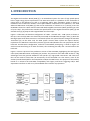
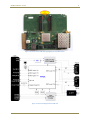
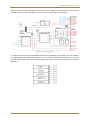
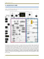
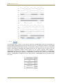
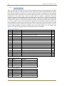
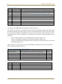
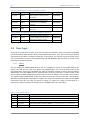
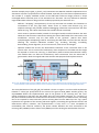
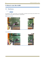
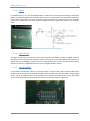
CERN PH-ESE-BE
GLIBv3 user manual
version
1.09
2013.02.19
GLIB project homepage: https://espace.cern.ch/project-GBLIB/public
Contact: [email protected]
2
GLIBv3 User Manual - draft
Document History
•
V1.09, 2012.02.19: Updated documentation for release_v3.1.0 and above.
•
V1.00, 2012.12.20: First draft in the document history.
GLIB team
Manoel Barros Marin, Sophie Baron, Vincent Bobillier, Stefan Haas, Magnus Hansen, Markus Joos,
Patrick Petit, Francois Vasey & Paschalis Vichoudis.
v1.09
GLIBv3 manual - draft
3
Table of Contents
Document History ................................................................................................................................... 2
GLIB team ................................................................................................................................................ 2
Table of Contents .................................................................................................................................... 3
1.
INTRODUCTION ............................................................................................................................... 4
2.
ARCHITECTURE ................................................................................................................................ 7
2.1
2.1.1
PLL & Reset controller ..................................................................................................... 8
2.1.2
Gigabit Ethernet and IPbus ............................................................................................. 8
2.1.3
SoC bus ............................................................................................................................ 9
2.1.4
System Registers ........................................................................................................... 10
2.2
3.
User Logic .............................................................................................................................. 14
2.2.1
SRAM ............................................................................................................................. 14
2.2.2
FMC I/O ......................................................................................................................... 16
2.2.3
Wishbone bus ............................................................................................................... 16
2.2.4
GBT-based links ............................................................................................................. 17
How to use the GLIB...................................................................................................................... 22
3.1
Hardware .............................................................................................................................. 22
3.1.1.
Jumpers ......................................................................................................................... 22
3.1.2.
Switches ........................................................................................................................ 23
3.1.3.
Powering ....................................................................................................................... 24
3.1.4.
Configuration ................................................................................................................ 24
3.1.5.
Reset ............................................................................................................................. 25
3.1.6.
RJ45 socket .................................................................................................................... 25
3.1.7.
Serial Number ............................................................................................................... 25
3.1.8.
LEDs ............................................................................................................................... 26
3.2
4.
System Core ............................................................................................................................ 8
Firmware/Software ............................................................................................................... 27
REFERENCES .................................................................................................................................. 29
APPENDIX A: GLIB v3 bench VTRx reference design ............................................................................. 31
v1.09
4
GLIBv3 User Manual - draft
1. INTRODUCTION
The Gigabit Link Interface Board (GLIB) [1] is an FPGA-based system for users of high speed optical
links in high energy physics experiments. The GLIB serves both as a platform for the evaluation of
optical links in the laboratory as well as a triggering and/or data acquisition system in beam or
irradiation tests of detector modules. The major hardware component of the platform is the GLIB
Advanced Mezzanine Card (AMC) [2] that can be used either on a bench or in a μTCA [3] crate. The
GLIB AMC is based on a Xilinx Virtex-6 FPGA with Multi-Gigabit Transceivers (MGT) operating at rates
of up to 5 Gb/s. This performance matches the specifications of the Gigabit Transceiver (GBT) [4] and
Versatile Link [5] [6] projects with targeted data rate of 4.8 Gb/s.
Figure 1-1 illustrates the baseline configuration of a GBT - Versatile Link - GLIB system is shown at
the top. Front-end (FE) ASICs are electrically connected to the GBT ASIC through e-links [7] while the
GBT high-speed serial data-streams are converted to/from the optical domain through the Versatile
Transceiver [8]. At the other end, the GLIB system converts data to/from the optical domain,
implements the GBT data transmission protocol [9] and codes/decodes the user payload at the link
back-end. An alternative configuration, useful for intermediate prototyping, is shown in Figure 1-2
with one GLIB interfacing to FE ASICs and VTRx, thus emulating the GBT, and a second GLIB at the
back-end.
Figure 1-3 shows a picture of the production version of the GLIB AMC, highlighting the two high-pin
count (HPC) FMC Mezzanine Card (FMC) [10] sockets. The presence of the HPC FMC sockets is a big
advantage since they provide additional user-specific I/O, high-speed transceivers and clock lines
that can be used to extend the I/O connectivity of the GLIB AMC. For that reason, most of the
auxiliary boards developed for the GLIB platform adopt the FMC format. The purpose of the auxiliary
boards is to enhance the GLIB AMC compatibility with legacy and future triggering and/or data
acquisition interfaces as well as its I/O bandwidth when in bench-top operation.
.
Figure 1-1: A GBT - Versatile Link system with the GLIB at the back-end.
Figure 1-2: A GLIB interfacing to FE ASICs and VTRx with a second GLIB at the back-end.
v1.09
GLIBv3 manual - draft
5
Figure 1-3: Picture of the GLIB AMC, highlighting the two FMC sockets
Figure 1-4: The block diagram of the GLIB card
v1.09
6
GLIBv3 User Manual - draft
Figure 1-5 shows a detailed diagram of the clock circuitry which is an essential part of the system.
The MGT reference clocks and fabric clocks are shown in red and black, respectively.
Figure 1-5: The clocking circuitry
It is important to mention that each MGT Reference clock (REFCLK) can be used to clock the MGT of
its neighbouring MGT Quads (see Figure 1-6). For instance, the REFCLK0 of the MGT 114 can also
clock the MGT quads 113 and 115. Details about the Virtex-6 clocking resources can be found in
Figure 1-6.
Figure 1-6: The MGT quads
v1.09
GLIBv3 manual - draft
7
2. ARCHITECTURE
Figure 2-1 illustrates the FPGA firmware architecture of the GLIB that is organized in two main parts,
the system_core and the user_logic.
Figure 2-1: Firmware architecture.
The system_core firmware instantiates a simple IP-based control protocol (IPbus) designed for
controlling xTCA-based hardware over Gigabit Ethernet that includes all basic transactions needed
for this purpose (bitwise, single register and block transactions) [10]. The system_core also includes
all interfaces to the on-board hardware e.g. I2C communication with the on-board temperature
sensors and the serial memory, SPI communication with clock synthesizer, SRAM interface with the
two (operating at up to 160MHz) etc. In order to interface the GLIB with GBT protocol based
systems, the GLIB firmware distribution provides GBT Hardware Description Language (HDL)
modules [13] and associated optional Gigabit Transceiver (GTX) ready to be instantiated as is inside
the user_logic.
v1.09
8
GLIBv3 User Manual - draft
2.1 System Core
2.1.1
PLL & Reset controller
The system_core contains a PLL which is clocked by the on-board 125MHz oscillator. The PLL
provides a 62.5MHz clock which is used for the internal bus of the system (see §2.1.3) as well as a
125MHz clock for the Gigabit Ethernet MAC instantiations. The Reset controller generates a master
reset pulse in the following cases:
-
During power up (detected by the Voltage Supervisor)
When the reset button is pressed (detected by the Voltage Supervisor).
When the FPGA firmware is reloaded (internal logic).
When the above mentioned PLL is not locked.
Both clocks (62.5MHz and 125MHz) as well as the reset pulse are forwarded to the user_logic block.
2.1.2
Gigabit Ethernet and IPbus
For the Gigabit Ethernet links, MAC cores are instantiated. In the case of bench-top operation, the
MAC core is configured as 1000Base-T in order to communicate with the external PHY. In the case of
crate operation, the two MAC cores (AMC P0 & P1 1) are configured as 1000Base-X for interfacing
with the Gigabit Ethernet Switch carried on the crate’s MCH.
For every MAC core, an IPbus endpoint is also instantiated. The IPbus system allows the control of
hardware via a ‘virtual bus’, using a standard IP-over-gigabit-Ethernet network connection. The IPbus
specifies a simple transaction protocol between the hardware and a software controller, which
assumes an A32/D32 connection to slave devices connected to the hardware endpoint. The current
IPbus firmware implementation is using a UDP/IP protocol and a simple synchronous SoC bus [12].
This protocol is based upon the Wishbone SoC protocol [13], and is compatible with Wishbone cores.
However, there are two important differences:
-
The master is not required to explicitly deassert strobe between cycles. However, it is
guaranteed to deassert strobe or begin the new cycle on the clock cycle following ack.
-
Slaves are not allowed to tie ack high, and must deassert ack on the same clock cycle that
strobe is deasserted. However, it is allowed to tie ack to strobe, if a zero-wait-state response
is always possible.
Timing diagrams of read and write transactions for a slave with and without wait states are given
below. The first diagram illustrates a write cycle to a slave with one wait state; the bus idle for two
clock cycles; then a read to a slave with zero wait states. The second diagram illustrates a ReadModify-Write transaction with a slave with zero wait states, followed immediately by two reads from
a slave with one wait state.
The reason of developing this custom SoC bus is to increase the bus efficiency by minimizing the
dead-time.
Please note that IP & MAC addresses are defined in the user_logic block.
1
The generation of AMC P1 MAC core when in crate mode is optional
v1.09
GLIBv3 manual - draft
9
Figure 2-2: IPbus read/write transactions [12]
2.1.3
SoC bus
As mentioned in §2.1.2, there is a case where more than one MAC/IPbus cores are instantiated. For
deciding which Gigabit Ethernet link will take over the bus, an Arbitration module is instantiated
between the IPbus cores and the bus fabric. The bus fabric redirects the bus to only one of the slave
devices instantiated by decoding the address (based on the memory map of Figure 2-3). The
system_core instantiates various system slaves e.g. the system registers (base address =
0x00000000), SRAM1 (base address = 0x02000000) and SRAM2 (base address = 0x04000000).
Additionally, the system_core allocates a large memory space for user slaves; IPbus slaves (base
address = 0x40000000) and Wishbone slaves (base address = 0x80000000) that can be added to the
user_logic.
Figure 2-3: Memory map
v1.09
10
GLIBv3 User Manual - draft
2.1.4
System Registers
Table 2-1 shows the 16 registers that are currently implemented into the System Registers HDL block
providing their address, a short description of their functionality and their type (Read-Write or Readonly). The 4-byte Board_ID register, as its name suggests, provides an identifier of the GLIB board
(0x474C4942). When the 4 bytes of the identifier are represented in ASCII characters, the identifier
corresponds to the word “GLIB”. Table 2-2 shows how the register is organized. The 4-byte
System_ID register declares GLIB’s mode of operation (bench-top or crate). For bench-top mode, the
register contains the value 0x4C414220 that corresponds to “LAB” when the 4 bytes are represented
in ASCII format. When in crate mode, the register contains the value 0x75544341 that corresponds
to “'uTCA”. Table 2-3 shows how the register is organized. The Firmware_ID register contains the
date (YY/MM/DD) and the version number of the firmware (major.minor.build). The register TestReg
is used only for testing the read/write transactions since it is not connected to the system_core logic.
The Ctrl register (Table 2-5) is used to configure the clock circuitry (Figure 1-5). The register Ctrl2
(Table 2-7) is used for loading firmware from the Platform Flash on demand.
Table 2-1: System Registers
Addr
Name
Description
Type
0x00
Board_ID
The board identifier code
RO
0x01
System_ID
The system identifier code
RO
0x02
Firmware_ID
The firmware date and version number
RO
0x03
TestReg
Register for test purposes only
RW
0x04
Ctrl
Controls the external clocking circuitry
RW
0x05
Ctrl2
Flash control
RW
0x06
Status
Status from various external components
RO
0x07
Status2
Currently not used
RO
0x08
Ctrl_SRAM
SRAM interface: Control
RW
0x09
Status_SRAM
SRAM interface: Status
RO
0x0A
SPI_txdata
SPI interface: data from FPGA to clock synthesizer
RW
0x0B
SPI_command
SPI interface: configuration (polarity, phase, frequency etc)
RW
0x0C
SPI_rxdata
SPI interface: data from clock synthesizer to FPGA
RO
0x0D
I2C_settings
I2C interface: configuration (bus select, frequency etc)
RW
0x0E
I2C_command
I2C interface: transaction parameters (slave address, data to slave etc)
RW
0x0F
I2C_reply
I2C interface: transaction reply (transaction status, data from slave etc)
RO
Table 2-2: Board_ID Register
bit(s)
Name
Description
[7:0]
board_id_char4
Board ID 4th character (ASCII code)
[15:8]
board_id_char3
Board ID 3rd character (ASCII code)
[23:16]
board_id_char2
Board ID 2nd character (ASCII code)
[31:24]
board_id_char1
Board ID 1st character (ASCII code)
Table 2-3: System_ID Register
bit(s)
Name
Description
[7:0]
system_id_char4
System_ID 4th character (ASCII code)
[15:8]
system_id_char3
System_ID 3rd character (ASCII code)
[23:16]
system_id_char2
System_ID 2nd character (ASCII code)
[31:24]
system_id_char1
System_ID 1st character (ASCII code)
v1.09
GLIBv3 manual - draft
11
The Status register (Table 2-8) is providing status information from various external components.
The register Status2 is reserved for future use.
Table 2-4: Firmware_ID Register
bit(s)
Name
Description
[31:28]
firmware_id_VER_MAJOR
Firmware version (major)
[27:24]
firmware_id_VER_MINOR
Firmware version (minor)
[23:16]
firmware_id_VER_BUILD
Firmware version (build)
[15:9]
firmware_id_YY
Firmware year (0-99)
[8:5]
firmware_id_MM
Firmware month
[4:0]
firmware_id_DD
Firmware day
Table 2-5: Ctrl Register
bit(s)
Name
Description
[0]
pcie_clk_fsel
ICS874003 output multiplication factor. 0 -> OUT = 2.5 x IN. 1 -> OUT =1.25 x IN.
[1]
pcie_clk_mr
ICS874003 master reset. 1 -> reset. 0 -> normal operation.
[2]
pcie_clk_oe
ICS874003 output enable. 1 -> outputs enabled. 0 -> outputs disabled.
[4]
cdce_powerup
CDCE62005 Control: power up of. 0 -> power down. 1 -> power up.
[5]
cdce_refsel
CDCE62005 Control: Clock input selection. 1 -> CLK1. 0 -> CLK2.
[6]
cdce_sync
CDCE62005 Control: synchronization. A transition from 0 to 1 is needed to resync.
[7]
cdce_ctrl_sel
Select who drives the control of the CDCE62005. 0 -> System_core. 1 -> user logic.
[8]
tclkb_dr_en
Enables the TCLKB output towards the backplane. 0 -> off. 1 -> on
[12]
xpoint2_s10
Input select for IC23 (SN65LVDT125) OUT1. See Table 2-6
[13]
xpoint2_s11
Input select for IC23 (SN65LVDT125) OUT1. See Table 2-6
[16]
xpoint1_s10
Input select for IC28 (SN65LVDT125) OUT1. See Table 2-6
[17]
xpoint1_s11
Input select for IC28 (SN65LVDT125) OUT1. See Table 2-6
[18]
xpoint1_s20
Input select for IC28 (SN65LVDT125) OUT2. See Table 2-6
[19]
xpoint1_s21
Input select for IC28 (SN65LVDT125) OUT2. See Table 2-6
[20]
xpoint1_s30
Input select for IC28 (SN65LVDT125) OUT3. See Table 2-6
[21]
xpoint1_s31
Input select for IC28 (SN65LVDT125) OUT3. See Table 2-6
[22]
xpoint1_s40
Input select for IC28 (SN65LVDT125) OUT4. See Table 2-6
[23]
xpoint1_s41
Input select for IC28 (SN65LVDT125) OUT4. See Table 2-6
Table 2-6: xpoint1 input select
Sx0
Sx1
Select Input
Example
0
0
IN_1 (see Figure 1-5)
When S40 = 0 & S41 = 0 then IN_1 -> OUT_4
0
1
IN_2 (see Figure 1-5)
When S40 = 0 & S41 = 1 then IN_2 -> OUT_4
1
0
IN_3 (see Figure 1-5)
When S40 = 1 & S41 = 0 then IN_3 -> OUT_4
1
1
IN_4 (see Figure 1-5)
When S40 = 1 & S41 = 1 then IN_4 -> OUT_4
Table 2-7: Ctrl2 Register
bit(s)
Name
Description
[1:0]
flash_firmware_page
Selects one of the 4 possible pages of the Platform Flash XL
[4]
Load_flash_firmware
Loads the firmware from the selected page
v1.09
12
GLIBv3 User Manual - draft
Table 2-8: Status Register
bit(s)
Name
Description
[2:0]
glib_sfp1_status[2:0]
on-board SFP1 status. bit[0] -> Mod_abs. bit [1] -> RxLOS. bit [2] -> TxFault.
[6:4]
glib_sfp2_status[2:0]
on-board SFP2 status. bit [0] -> Mod_abs. bit [1] -> RxLOS. bit [2] -> TxFault.
[10:8]
glib_sfp3_status[2:0]
on-board SFP3 status. bit [0] -> Mod_abs. bit [1] -> RxLOS. bit [2] -> TxFault.
[14:12]
glib_sfp4_status[2:0]
on-board SFP4 status. bit [0] -> Mod_abs. bit [1] -> RxLOS. bit [2] -> TxFault.
[16]
gbe_int
Interrupt request from GbE PHY. 0 -> no interrupt. 1 -> interrupt
[17]
fmc1_presence
Presence of FMC1. 1-> yes, 0-> no
[18]
fmc2_presence
Presence of FMC2. 1-> yes, 0-> no
[19]
fpga_reset
state of the fpga_reset line (driven by the CPLD)
[25:20]
v6_cpld
state of the 6-bit bus between the FPGA and the CPLD
[28]
cdce_lock
Status of CDCE62005. 1 -> locked. 0 -> unlocked
The registers Ctrl_SRAM and Status_SRAM are presented in §2.2.1.
The registers I2C_settings, I2C_command and I2C_reply are controlling the operation of the dual-bus
I2C master controller that can be used to access the on-board I2C devices when in bench-top mode
(in crate mode, the MMC is responsible for that task). Table 2-9 presents the I2C devices and their
corresponding I2C 7-bit slave addresses. The operation of the above mentioned registers is the
following:
-
The I2C_settings register used for configuring the controller (Table 2-10).
The I2C_command for setting the I2C transaction parameters (Table 2-11).
The I2C_reply provides the transaction status as well as data sent by the slave in case of read
transactions (Table 2-12).
Table 2-13 gives an example list of transactions needed for reading the temperature of the FPGA
with an I2C bus frequency of 62.5kHz.
Table 2-9: The I2C devices and their 7-bit slave addresses
I2C Device
Description
I2C Address
24AA025E48 EEPROM
256x8bit EEPROM with unique 48-bit serial number (EUI-48)
1010110
LM82 Temperature sensor #1
Provides the temperature of the FPGA’s die at reg1 [addr:0x01]
0101010
LM82 Temperature sensor #2
Provides the pcb temperature at the front at reg0 [addr:0x00]
0011010
LM82 Temperature sensor #3
Measures the pcb temperature at the rear at reg0 [addr:0x00]
1001110
FMC#1
The I2C devices hosted on the FMC#1
XXXXX00
FMC#2
The I2C devices hosted on the FMC#2
XXXXX11
Table 2-10: “I2C_settings” register
bit(s)
Name
Description
[9:0]
i2c_prescaler
I2C clock prescaler. I2C clk (kHz)=62500/i2c_prescaler
[10]
i2c_bus_select
Select I2C bus. 1 -> I2C for PHY. 0 -> I2C for all other devices.
[11]
i2c_enable
Enable I2C controller. 1 -> enabled. 0 -> disabled.
[12]
reserved
Reserved. Keep it always at 0
v1.09
GLIBv3 manual - draft
13
Table 2-11: “I2C_command” register
bit(s)
Name
Description
[7:0]
Wrdata
Byte to write to the i2c slave.
[15:8]
reserved
Reserved. Keep always to 0.
[22:16]
slv_addr
The 7-bit slave address
[23]
wr_en
Write enable. 0 -> Read transaction. 1 -> Write transaction.
[24]
reserved
Reserved. Keep always to 0.
[25]
mode16b
16bit operation (for PHY only). 0 -> standard 8-bit mode. 1 -> 16bit mode
[31]
i2c_strobe
Execute Transaction strobe signal. It clears automatically. Keep it always to 1.
Table 2-12: “I2C_reply” register
bit(s)
Name
Description
[7:0]
rddata_lo
Byte read from the i2c slave. Low byte in case of 16-bit mode
[15:8]
rddata_hi
High byte read from the i2c slave in case of 16-bit mode
[27:26]
i2c_status[1:0]
Transaction status. 01 -> succeed. 11 -> failed. 00 -> pending. 10 -> pending.
Table 2-13: Example transaction list for reading the temperature of the FPGA’s die
Register
Access
Description
Value (hex)
i2c_enable -> 1,
I2C_settings
WRITE
i2c_bus_sel -> 0,
0x00000BE8
i2c_prescaler -> 1000
wr -> 1, mode16b -> 0, slv_addr -> 0x2A
I2C_command WRITE
0x80AA0001
wrdata -> 0x01 (select LM82’s register#1)
I2C_reply
READ
Verify the transaction status
wr -> 0, mode16b -> 0, slv_addr -> 0x2A,
I2C_command WRITE
0x802A0000
wrdata -> don't care
Verify the transaction status. If successful,
I2C_reply
READ
the temperature will be available in
rddata_lo
i2c_enable -> 0,
I2C_settings
WRITE
i2c_bus_sel -> don't care,
0x00000000
i2c_prescaler -> don't care
The registers SPI_txdata, SPI_command and SPI_rxdata are controlling the operation the SPI master
controller that is used for the configuration of the CDCE62005 clock synthesizer. The operation of
the above mentioned registers is the following:
-
The SPI_txdata where the 32-bit word to be transmitted to the SPI slave is defined.
The SPI_rxdata where the 32-bit word transmitted by the SPI slave is presented.
The SPI_command where the SPI master’s configuration is defined as well as the transaction
parameters (Table 2-14).
Table 2-15 shows an example list of transactions for reading one of CDCE62005’s registers. Table
2-16 shows an example of writing one of CDCE62005’s registers.
Table 2-14: The SPI_command register
bit(s)
Name
[11:0]
spi_prescaler
[27:12]
reserved
[31]
spi_strobe
Description
SPI clock prescaler.
SPI clk (MHz)=62.5/spi_prescaler. Suggested value: 0x014
Reserved.
Keep always to 0xFA38.
Execute Transaction strobe signal. It clears automatically.
Keep it always to 1.
v1.09
14
GLIBv3 User Manual - draft
Table 2-15: Transaction list for reading CDCE62005’s Register 8
Register
Access
Description
Set the value that corresponds to the
SPI_txdata
WRITE
reading register 8 command of the
CDCE62005
SPI_command WRITE
Execute the transaction
Set a dummy value that does not
SPI_txdata
WRITE
corresponds to any CDCE62005
command
SPI_command WRITE
Execute the transaction
The contents of CDCE62005’s Register 8
SPI_rxdata
READ
appear here
Table 2-16: Example transaction list for writing CDCE62005’s Register 0
Register
Access
Description
Set the value to write to Register 0.
SPI_txdata
WRITE
Note that bits[3:0] must be zero for
addressing the register correctly
SPI_command WRITE
Execute the transaction
Value (hex)
0x0000008E
0x8FA38014
0xAAAAAAAA
0x8FA38014
Value (hex)
0xEB840720
0x8FA38014
2.2 User Logic
From the user_logic point of view, there are two types of interfaces, direct connections with FPGA
pins and interfaces with firmware blocks instantiated in the system_core. The use of the pins directly
connected to the FPGA is straight forward (just if the system_core and the top level did not exist).
This section focuses in the use of the SRAM, FMC I/O and Wishbone bus interfaces as well as in the
instantiation of GBT-based links.
2.2.1
SRAM
The two single-port 2Mx36 SRAM devices that are available on board are accessible both by the
system_core and the user_logic. The register Ctrl_SRAM (Table 2-17) is used to select which of the
two blocks takes control over the SRAM, the mode of operation (normal or Built-In Self Test (BIST)).
Additionally, since the SRAM2 and the FLASH memory share the same bus, it selects which of the
two memories is addressed (please note that the access of the FLASH is not covered in this section).
The register Status_SRAM (Table 2-18) is used only to report the results of the BIST. Logic Analyzer
Waveforms captured with Chipscope for single write, single read, block write and block read SRAM
transactions from the user_logic are shown in Figure 2-4, Figure 2-5, Figure 2-6 and Figure 2-7,
respectively. Figure 2-8 shows an example use of an SRAM in the user_logic block.
Table 2-17: “Ctrl_SRAM” register
bit(s)
Name
Description
[0]
user_ctrl_sram1
Selects who is taking over the SRAM1 bus. 0 -> system_core. 1 -> user_logic.
[1]
bist_sram1
Built-in Self Test (BIST) Enable for SRAM1. 0 -> normal operation. 1 -> run the BIST.
[16]
user_ctrl_sram2
Selects who is taking over the SRAM2 bus. 0 -> system_core. 1 -> user_logic.
[17]b
bist_sram2
Built-in Self Test (BIST) Enable for SRAM2. 0 -> normal operation. 1 -> run the BIST.
[20]
flash_select
Selects between SRAM2 & FLASH. 0 -> SRAM2. 1 -> FLASH.
v1.09
GLIBv3 manual - draft
15
Table 2-18: “Status_SRAM” register
bit(s)
Name
Description
[0]
bist_done_sram1
SRAM1 BIST completed flag. 0 -> test pending. 1 -> test completed.
[1]
bist_status_sram1
SRAM1 BIST status flag. 0 -> test failed. 1 -> test passed.
[16]
bist_done_sram2
SRAM2 BIST completed flag. 0 -> test pending. 1 -> test completed.
[17]
bist_status_sram2
SRAM2 BIST status flag. 0 -> test failed. 1 -> test passed.
Figure 2-4: User_logic SRAM single write
Figure 2-5: User_logic SRAM single read
Figure 2-6: User_logic SRAM block write
v1.09
16
GLIBv3 User Manual - draft
Figure 2-7: User_logic SRAM block read
Figure 2-8: Example use of the SRAM in the user_logic file
2.2.2
FMC I/O
All FMC I/Os are directly connected to the user_logic block and can be configured independently as
LVCMOS 2.5V or LVDS inputs or outputs by simply instantiating the corresponding Xilinx primitive
buffer such as IBUF, OBUF, IOBUF, IBUFDS, OBUFDS etc. (see Figure 2-9).
Figure 2-9: Example I/O buffer instantiation in the user_logic for the LA15_P line of FMC1 using Xilinx primitives
2.2.3
Wishbone bus
The user has the possibility to instantiate wishbone-compatible slaves inside the user_logic as well as
to attach them on the wishbone bus available. Figure 2-10 shows an example of how to declare the
total number of wishbone slaves (and their symbolic names). Figure 2-11 shows the address
mapping of the wishbone slaves. Figure 2-12 illustrates an example of a wishbone slave instantiation
in the user_logic. Example wishbone slaves can be found in the example projects available.
v1.09
GLIBv3 manual - draft
17
Figure 2-10: Wishbone slave declaration (user_package)
Figure 2-11: Example wishbone slave address mapping (user_addr_decode.vhd)
Figure 2-12: Example instantiation of a wishbone slave in the user_logic file
2.2.4
GBT-based links
As mentioned in the introduction, one of the principle use cases of the GLIB is to be part of a GBT –
Versatile Link system for evaluation purposes. For that reason, the GLIB firmware release includes a
couple of example projects instantiating GBT-based links in the user_logic block. One of the example
projects (glib_v3_bench_gbt_fpga) instantiates the GBT-FPGA reference design targeted for the
ML605 Virtex-6 development kit as is. The source files and associated documentation can be found
in [16].
v1.09
18
GLIBv3 User Manual - draft
Another example project (glib_v3_bench_vtrx) instantiates two GBT-link modules implemented in an
alternative way that is proposed for use with the GLIB, especially for multi-channel implementations.
This module is a slightly modified version of the GBT-FPGA reference design however it keeps
unchanged all the essential parts of the GBT-FPGA core firmware. The only differences between
original GBT-FPGA reference design and the module proposed by the GLIB team are:
-
Different “wrapping” (encapsulation) of the top level GBT link module that facilitates its
instantiation in the user_logic block, allows access to various GTX features (e.g. preemphasis settings) and provides additional debugging information extracted from the GBTFPGA core (e.g. the 120-bit data frame that includes the FEC overhead).
-
Clock resource optimized 20-bit (instead of the original 40-bit) interface between the GBTFPGA core and the Virtex-6 GTX thus matching the natural data width of the transceiver. This
modification concerns only the data width of the “gearbox” (120-bit data frame
multiplexing/de-multiplexing) used for interfacing the GBT-FPGA core with the GTX without
affecting the essential GBT-FPGA modules (e.g. encoding, decoding, scrambling,
descrambling, frame alignment, error correction etc.) that remain unchanged.
-
Optional module that ensures the deterministic behaviour of the recovered clock in the
receiver side. This is essential for fixed-latency data reception on the FPGA side that might
be required in certain use cases (e.g. a fixed-latency FPGA-to-FPGA communication setup).
This module does not affect the fixed-latency data transmission from the FPGA that is
guaranteed in both the original GBT-FPGA and the GLIB proposed link implementations.
Figure 2-13: Simplified diagram of the GLIB GBT link block. The arrows in black show the principle data ports. The arrows
in blue illustrate control interfaces and the ones in red show internal data connections & debugging information.
The entity declaration of the glib_gbt_link module is shown in Figure 2-14. The module implements
between 1-4 links (per quad) based on the value of the generic NUM_LINKS. Another generic, the
RX_GEARBOX defines the implementation type of the gearbox at the receiving end. The “ram”
option implements a dual port ram with 20-bit write port and 120-bit read port. It is “immune” to
the phase relation between the read and write clocks but its latency is not deterministic, something
that is not required for most back-end systems receiving data from the GBTx chip. The “reg” option
implements the gearbox of the receiving side with registers, something that guarantees shorter and
deterministic latency. However, this implementation is tricky since it is more susceptible to
metastability that could be caused by the phase relation between the clock recovered at the
receiving side (240MHz) and the frame clock (40MHz) used for clocking the GBT decoder firmware.
v1.09
GLIBv3 manual - draft
19
Figure 2-14: Entity declaration of glib_gbt_link
Since the module has a large number of I/O ports, they are organized in “records”, the following:
CLK_I: Input clocks of the module
interface_clk
gtx_tx_refclk
gtx_rx_refclk
tx_frame_clk
rx_frame_clk
drp_dclk
:
:
:
:
:
:
the
the
the
the
the
the
clock of the control bus used (Wishbone or IPbus)
reference clock for the Tx side of the GTX (see Xilinx’s UG366)
reference clock for the Rx side of the GTX (see Xilinx’s UG366)
clock of the GBT Tx core (often referred-to as GBT encoder)
clock of the GBT Rx core (often referred-to as GBT decoder)
clock for the dynamic reconfiguration interface (see Xilinx’s UG366)
CLK_O: Output clocks of the module
tx_word_clk
rx_word_clk
: the clock that feeds the Tx gearbox
: the Rx recovered clock(s) that feed the Rx gearbox(es)
GBT_ENC_I: Input signals of the GBT encoder
reset
data
: resets the logic of the encoder
: the 84-bit data payload input
GBT_ENC_O: Output signals of the GBT encoder
frame
word
header
: copy of the intermediate 120-bit scrambled frame incl. Header & FEC overhead
: copy of the 20-bit word fed to the Tx portion of the GTX
: copy of the flag indicating that the current 20-bit word contains the 4-bit header
GBT_DEC_I: Input ports of the GBT decoder
reset
: resets the logic of the GBT decoder
GBT_DEC_O: Output ports of the GBT decoder
aligned
data
data_dv
bit_slip_cmd
bit_slip_nbr
:
:
:
:
:
flag indicating that the GBT decoder is aligned (locked) to the incoming data
the decoder 84-bit data payload output
flag indicating that the payload is valid
copy of the request for a new bitslip during alignment
copy of the total number of bitslips (shifts) performed by the GBT aligner
v1.09
20
GLIBv3 User Manual - draft
shiftedword
header_flag
write_address
frame_dv
frame
:
:
:
:
:
copy
copy
copy
copy
copy
of
of
of
of
of
the aligned 20-bit word (result of the bitslip operation)
the flag indicating that the current 20-bit word contains the 4-bit header
the Rx gearbox write address
the flag indicating that the 120-bit frame is valid
120-bit output frame of the Rx gearbox
GTX_I: Input ports of GTX transceivers
rxp
rxn
Loopback
tx_powerdown
rx_powerdown
rx_reset
rx_sync_reset
tx_reset
tx_sync_reset
drp_daddr
drp_den
drp_di
drp_dwe
conf_diff
conf_pstemph
conf_preemph
conf_txpol
conf_rxpol
conf_eqmix
prbs_txen
prbs_rxen
prbs_forcerr
prbs_errcntrst
rx_slide_enable
rx_slide_ctrl
rx_slide_run
rx_slide_nbr
:
:
:
:
:
:
:
:
:
:
:
:
:
:
:
:
:
:
:
:
:
:
:
:
:
:
:
GTX Rx input (positive)
GTX Rx input (negative)
GTX loopback control (see Xilinx’s UG366)
power-down the Tx portion of the GTX transceiver (see Xilinx’s UG366)
power-down the Rx portion of the GTX transceiver (see Xilinx’s UG366)
global reset of the Rx portion of the GTX transceiver (see Xilinx’s UG366)
reset of the GTX Rx synchronization state machine (see Xilinx’s UG366)
global reset of the TX portion of the GTX transceiver (see Xilinx’s UG366)
reset of the GTX Tx synchronization state machine (see Xilinx’s UG366)
dynamic reconfiguration interface (see Xilinx’s UG366)
dynamic reconfiguration interface (see Xilinx’s UG366)
dynamic reconfiguration interface (see Xilinx’s UG366)
dynamic reconfiguration interface (see Xilinx’s UG366)
Tx differential swing settings (see Xilinx’s UG366)
Tx post-emphasis settings (see Xilinx’s UG366)
Tx pre-emphasis settings (see Xilinx’s UG366)
Tx polarity control (see Xilinx’s UG366)
Rx polarity control (see Xilinx’s UG366)
Rx equalization control (see Xilinx’s UG366)
built-in prbs interface (see Xilinx’s UG366)
built-in prbs interface (see Xilinx’s UG366)
built-in prbs interface (see Xilinx’s UG366)
built-in prbs interface (see Xilinx’s UG366)
the control of the GTX Rx slide operation (see below)
custom interface for the control of the GTX Rx slide operation (see below)
custom interface for the control of the GTX Rx slide operation (see below)
custom interface for the control of the GTX Rx slide operation (see below)
GTX_O: Output ports of GTX transceivers
txp
txn
resetdone
rx_data
drp_drdy
drp_drpdo
prbs_rxerr
phasealigndone
:
:
:
:
:
:
:
:
GTX Tx output (positive)
GTX Rx output (negative)
end of reset procedure
copy of the received 20-bit word fed to the GBT decoder
dynamic reconfiguration interface (see Xilinx’s UG366)
dynamic reconfiguration interface (see Xilinx’s UG366)
built-in prbs interface (see Xilinx’s UG366)
custom interface for the control of the GTX Rx slide operation (see below)
GTX Rx slide custom interface
As mentioned previously, the GLIB GBT link contains an optional module that ensures the
deterministic behaviour of the recovered clock in the GTX receiver side (if required). This module
takes advantage of a “hidden” operation mode of the Rx slide feature of the GTX (RX_SLIDE_MODE =
PMA) that is not available in the GTX wizard (see Xilinx’s UG366). This feature allows the control of
the phase of the recovered clock that is essentially the source of the non-deterministic data
reception on the FPGA side. The module has three modes of operation, the following:
v1.09
GLIBv3 manual - draft
21
1. “off”: The Rx slide is disabled
2. “auto”: The Rx slide is enabled. It runs at the rising edge of GBT_DEC_O.aligned and
performs a number of bitslips equal to GBT_DEC_O.bit_slip_nbr
3. “manual”: Runs on-request at the rising edge of GTX_I. rx_slide_run performing a number of
bitslips equal to GTX_I.rx_slide_nbr
The mode of operation is selected as shown in Table 2-19: Modes of operationTable 2-19. The
GTX_O.phasealigndone flag indicates that the procedure has been completed
Table 2-19: Modes of operation of the GTX RX slide custom interface
MODE
“off”
“auto”
“manual”
rx_slide_enable
0
1
1
rx_slide_ctrl
don’t care
0
1
v1.09
22
GLIBv3 User Manual - draft
3. How to use the GLIB
3.1 Hardware
3.1.1.
Jumpers
The operation mode of the GLIB is set up through two jumpers (J5 and J10). The position of the
jumpers for the two modes of operation is shown below.
Bench-top operation
Figure 3-1: Jumpers J5 and J10 set up for bench-top operation.
Crate operation
Figure 3-2: Jumpers J5 and J10 set up for crate operation.
v1.09
GLIBv3 manual - draft
23
External Clocking
As previously illustrated in Figure 1-5 and Figure 2-1, the GLIB features an SMA connector for
external clocking. The connection scheme of the SMA connector (SMA1) and the 40MHz crystal
oscillator (QZ2) of the GLIB is set up through the jumper J14. The default configuration sets the SMA
connector as input/output of the FPGA and the 40Mhz crystal oscillator as input for the cross point
switch 1 (IC28).
Figure 3-3: SMA/Jumper J14 picture (left). SMA and 40 MHz crystal oscillator (QZ2) setup block diagram (right)
3.1.2.
Switches
The default position of the DIP switches is as illustrated below. All other combinations are reserved.
Figure 3-4: Default switches positions.
v1.09
24
GLIBv3 User Manual - draft
3.1.3.
Powering
For bench-top operation, the GLIB can be powered through a socket compatible with the 12V 4-pin
connector that is typically available in ATX compatible power supplies (Error! Reference source not
found. left and right, respectively). In case of ATX power supply use, the PS-ON pin of the 20-pin ATX
connector must be connected to ground as shown in Figure 3-6 (bottom) in order to start-up the
power supply.
Figure 3-5: Powering a GLIB with an ATX power supply.
Figure 3-6: How to start-up an ATX Power supply outside a computer.
3.1.4.
Configuration
The GLIB features two JTAG connectors. J13 configures the CPLD & J12 configures the FPGA.
Figure 3-7: JTAG connectors for configuring the CPLD (left) and FPGA (right).
v1.09
GLIBv3 manual - draft
3.1.5.
25
Reset
As mentioned in §2.1.1, the GLIB board features a button for resetting the FPGA logic. The button
(SW1) is located in between the two FMC sockets and it is connected to a TLC7725 power supervisor
(IC14). When the button is pressed, the power supervisor generates a pulse that is used to reset the
system_core. Additionally, the reset signal is forward to the user_logic block where it can be freely
used.
Figure 3-8: Reset button picture and reset scheme schematic.
3.1.6.
RJ45 socket
The RJ45 socket (and associated circuitry) carried by the GLIB board provides a Gigabit Ethernet
connection in case of bench-top operation. Please note that since the GLIB supports only Ethernet at
1Gbps (and not 10/100Mbps), please connect it using standard (not crossover) network cables either
directly to a PC with a Gigabit Ethernet card or to a Gigabit Ethernet switch.
3.1.7.
Serial Number
As previously mentioned in Table 2-9, the GLIB carries a serial memory with a 48-bit unique serial
number that could be used to identify the GLIB boards. Furthermore, the GLIB offers the possibility
to the user of an additional 8-bit serial number that is directly accessible from the user_logic block
and it can be hard-coded by placing up to 8 resistors on the pads shown in Figure 3-9.
Figure 3-9: Resistors pads for optional hard-coding of 8-bit serial number.
v1.09
26
GLIBv3 User Manual - draft
3.1.8.
LEDs
Figure 3-10: CPLD, FPGA user and system LEDs
System LED
The system core blinks the system LED (LD3) with a period of 1 second to indicate that the GLIB
firmware has been loaded correctly.
FPGA user LEDs
The FPGA user LEDs (LD4 and LD5) can be directly controlled by the logic placed on the user core.
CPLD LEDs
The LEDs LD6, LD7, LD8 are connected to the CPLD. The meaning of these LED may change between
versions of the CPLD firmware.
MMC LEDs
When in crate operation, the LEDs MMC_RED_LED (LD1), MMC_GREEN_LED (LD2) and
MMC_BLUE_LED (LD9) are controlled by the MMC and indicate the state of the GLIB.
Table 20: MMC LEDs and GLIB state relationship
GLIB state
MMC LEDs
Inactive
Active
MMC_RED_LED
ON
OFF
MMC_BLUE_LED
ON
OFF
MMC_GREEN_LED
OFF
ON
Figure 3-11: Inactive GLIB (left) and active GLIB (right)
v1.09
GLIBv3 manual - draft
27
3.2 Firmware/Software
Xilinx:
The GLIB team recommends using Xilinx ISE v13.2 for firmware development and implementation.
How to download:
Firstly go with a web browser at “https://svnweb.cern.ch/cern/wsvn/ph-ese/be/amc_glib/tags” and
identify the latest GLIBv3 release for firmware, software and documentation (amc_glib_fw_3_X_Y,
amc_glib_sw_A_B_C and amc_glib_doc_K_L_M, respectively). Please note only users with CERN
account can access the firmware.
Windows: Do a checkout with an SVN client (e.g. TortoiseSVN) from the following path:
Firmware:“https://svn.cern.ch/reps/ph-ese/be/amc_glib/tags/[amc_glib_fw_3_X_Y]”
Software:“https://svn.cern.ch/reps/ph-ese/be/amc_glib/tags/[amc_glib_sw_A._B_C]”
Documentation:“https://svn.cern.ch/reps/ph-ese/be/amc_glib/tags/[amc_glib_doc_K_L_M]”
Linux: type the following commands in a terminal
Firmware:“svn co https://svn.cern.ch/reps/ph-ese/be/amc_glib/tags/[amc_glib_fw_3_X_Y]”
Software:“svn co https://svn.cern.ch/reps/ph-ese/be/amc_glib/tags/[amc_glib_sw_A_B_C]”
Documentation:“svn co https://svn.cern.ch/reps/ph-ese/be/amc_glib/tags/[amc_glib_doc_K_L_M]”
The GLIB releases can also be accessed using a web browser at
“https://svnweb.cern.ch/cern/wsvn/ph-ese/be/amc_glib/tags”. Please note only users with CERN
account can download the firmware.
How to use the firmware:
For using the existing example code as is, simply compile the *.xise project files that can be found
under the fpga/prj. For developing your own code, please keep in mind that in order to receive
support from the GLIB team, the files under fpga/src/system MUST remain unchanged. On the other
hand, the files under the fpga/src/user can be freely modified according to the user needs.
Concerning the CPLD & MMC firmware, we provide the source files for your reference only and we
strongly suggest not modifying them.
How to use the software:
The software distribution contains several scripts in Python with self-explanatory names that are
performing basic transactions. The scripts are using the PyChips library [15] developed for accessing
IPbus based hardware in a simple way. In order to execute the scripts, please make that Python 2.x
(minimum Python 2.3) is installed. PyChips is NOT compatible with Python 3.x. For the correct
operation of the scripts, some variables have to be defined.
Under Windows, set the following environmental variables:
v1.09
28
GLIBv3 User Manual - draft
PYTHONPATH with value [software_installation_path]\[PyChips_distribution]\src such as
“E:\amc_glib_sw_A_B_C\Pychips_1_4_1\src”
PATH with value [Python_2.x_installation_path] e.g. “C:\Python27”
Under Linux, use the export command to define a variable with name PYTHONPATH and value
“$HOME/[software_installation_path]/[PyChips_distribution]/src:$PYTHONPATH”
e.g. “export PYTHONPATH=$HOME/PyChips_1_4_1/src:$PYTHONPATH”.
Additionally, in order to communicate successfully with the GLIB, the IP address of the Ethernet port
has to be set in order to be in the same subnet e.g. for the default GLIB address (192.168.0.111) the
configuration could be the following:
IP Address: 192.168.0.100
Subnet Mask: 255.255.255.0
In order to run the scripts, do the following:
Windows: go to the directory [software_installation_path]\[PyChips_distribution]\scripts, type the
script’s file name and press Enter.
Linux: go to the directory “$HOME/[software_installation_path]/[PyChips_distribution]/scripts“, type
the script’s file name and press Enter.
v1.09
GLIBv3 manual - draft
29
Brief description of the scripts:
glib_board_info.py: prints general board status information
glib_sysreg_test.py: example of r/w access of the system registers
glib_cdce_read.py: reads through SPI the contents of the CDCE62005 registers
glib_cdce_write.py: writes through SPI the GLIB default values to the CDCE62005 registers
glib_cdce_write_test_only.py: writes through SPI non-sense values to the CDCE62005 registers
glib_cdce_powerup_and_sync.py: power-cycles and synchronizes the CDCE62005
glib_sram1_read.py: reads the contents of the sram1, writes them to the tmp.txt and prints the first 32 values
glib_sram1_write.py: writes and incrementing by 1 value to all memory locations of sram1
glib_sram1_clear.py: writes “zeros” to all memory locations of sram1
glib_sram2_read.py: reads the contents of the sram1, writes them to the tmp.txt and prints the first 32 values
glib_sram2_write.py: writes and incrementing by 1 value to all memory locations of sram2
glib_sram2_clear.py: writes “zeros” to all memory locations of sram2
glib_i2c_eeprom_read_eui: reads the 48-bit serial number from the 24AA025E48 I2C EEPROM
glib_i2c_fmc_eeprom.py: example of r/w access of the I2C EEPROM carried by the FMC mezzanines
glib_i2c_temperature.py: reads the three on-board I2C temperature sensors
glib_phy_read.py: reads the registers of the M88E1111 PHY through I2C
glib_icap_interface_test.py: reads and writes several registers of the icap
glib_icap_trigg_fpga_conf_test.py: triggers the dynamic reconfiguration of the FPGA
glib_vtrx: enables the VTRx ref. design with the GTX transceivers set up for normal operation.
glib_vtrx_loopback: enables the VTRx ref. design with the GTX transceivers set up for loopback operation.
(See block diagram on Appendix B)
glib_flash_prom_wr: reads PROM file/writes FLASH or reads FLASH/dumps the content to a file
glib_flash_full_erase: completely erases the flash
4. REFERENCES
[1] P Vichoudis et al., The Gigabit Link Interface Board (GLIB), a flexible system for the evaluation
and use of GBT-based optical links 2010 JINST 5 C11007
[2] PICMG, AMC.0 R2.0 (November 15, 2006),
http://www.picmg.com/v2internal/specifications2.cfm?thetype=One&thebusid=1
[3] PICMG, MTCA.0 R1.0 (July 6, 2006),
http://www.picmg.com/v2internal/specifications2.cfm?thetype=One&thebusid=5
[4] P. Moreira et al., The GBT Project, in proceedings of the Topical Workshop on Electronics for
Particle Physics TWEPP 2009, CERN-2009-006
[5] L. Amaral et al., The versatile link, a common project for super-LHC, 2009 JINST 4 P12003
[6] F. Vasey et al., The versatile link common project: feasibility report, 2012 JINST 7 C01075
v1.09
30
GLIBv3 User Manual - draft
[7] S. Bonacini et al., e-link: A radiation-hard low-power electrical link for chip-to-chip
communication, in proceedings of the Topical Workshop on Electronics for Particle Physics
TWEPP2009, CERN-2009-006
[8] J. Troska et al., Versatile Transceiver developments, 2011 JINST 6 C01089
[9] S. Baron et al., Implementing the GBT data transmission protocol in FPGAs, in proceedings of
the Topical Workshop on Electronics for Particle Physics TWEPP-09, CERN-2009-006
[10] ANSI/VITA, 57.1-2008 (R2010), http://www.vita.com/fmc.html
[11] Rob Frazier et al., “Software and firmware for controlling CMS trigger and readout hardware
via gigabit Ethernet”, in proceedings of the Technology and Instrumentation in Particle
Physics TIPP 2011, to be published in Physics Procedia
[12] Dave Newbold, “Notes on Firmware Implementation of an IPbus SoC Bus”, draft, 16/5/2011
[13] OpenCores “Wishbone B4 Specification” Spec
[14] S. Baron et al., “Implementing the GBT data transmission protocol in FPGAs”, in proceedings
of the Topical Workshop on Electronics for Particle Physics TWEPP-09, CERN-2009-006
[15] PyChips web page http://projects.hepforge.org/cactus/trac/wiki/PyChips
[16] GBT-FPGA firmware releases Starter Kit Firmware Releases
v1.09
GLIBv3 manual - draft
31
APPENDIX A: GLIB v3 bench VTRx reference design
GLIB v3 bench VTRx reference design block diagram.
The glib_v3_bench_vtrx example project instantiates 2 GLIB GBT links (one mapped to an on-board
SFP and the other one mapped to a transceiver of the FMC1 socket), a pattern generator common
for both, registers (accessible through a user wishbone bus) for the control/monitoring of the links,
few simplified Bit-Error-Rate test modules (BERT) and other auxiliary modules (not shown in the
drawing above).
Please note that since the GBT coding scheme is very complicated and essentially not repeatable
(contrary to a PRBS sequence), the example BERT modules that are comparing the 20-bit words
cannot be fully automated, and therefore require manual configuration (please see the associated
vtrx_bert scripts for details). Their configuration depends on the length of the fiber used and the
type or Rx gearbox (ram- or register-based) since both parameters affect the loopback link latency.
For simplicity reasons, we used the same modules for the 84-bit frame comparison. If for any reason
you have doubts about the reliability of the BERT modules, please instantiate chipscope modules
and monitor the traffic manually.
Finally, it is worth mentioning that since the pattern generator in that example is common, the user
could either run both simple loopbacks (SFP->SFP & FMC1->FMC1) or crossed ones (SFP->FMC1 &
FMC1 -> SFP).
v1.09


![arXiv:1306.3436v1 [hep-ph] 14 Jun 2013](http://vs1.manualzilla.com/store/data/005779061_1-09962217330e865ae44dd3cb323f6311-150x150.png)