1
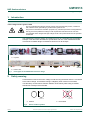
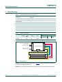
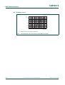
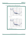
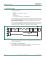
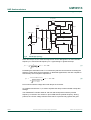
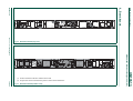
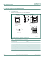
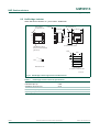
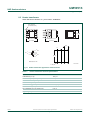
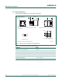
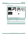
UM10513 UBA2015AT Reference Design 120 V (AC) Rev. 1.1 — 31 January 2012 User manual Document information Info Content Keywords UBA2015AT, dimmable, 2 × T5 35 W ballast Abstract This document describes the UBA2015AT reference design for 120 V (AC). This dimmable design drives two 35 W T5 lamps. This user manual describes the performances, technical data and wiring of the reference design. UM10513 NXP Semiconductors UBA2015AT Reference Design 120 V (AC) Revision history Rev Date Description v.1.1 20120131 second issue v.1 20111206 first issue Contact information For more information, please visit: http://www.nxp.com For sales office addresses, please send an email to: [email protected] UM10513 User manual All information provided in this document is subject to legal disclaimers. Rev. 1.1 — 31 January 2012 © NXP B.V. 2012. All rights reserved. 2 of 26 UM10513 NXP Semiconductors UBA2015AT Reference Design 120 V (AC) 1. Introduction WARNING Lethal voltage and fire ignition hazard The non-insulated high voltages that are present when operating this product, constitute a risk of electric shock, personal injury, death and/or ignition of fire. This product is intended for evaluation purposes only. It shall be operated in a designated test area by personnel qualified according to local requirements and labor laws to work with non-insulated mains voltages and high-voltage circuits. This product shall never be operated unattended. The UBA2015AT reference design is intended to serve as a dimmable two lamp ballast example. This document describes the specification and use of the UBA2015AT board. This reference ballast design is intended to drive two T5 35 W lamps. aaa-001136 a. top view. b. bottom view. Fig 1. Photograph of the UBA2015AT reference design 2. Safety warning Connected the board to the mains voltage. Avoid touching the board while it is connected to the mains voltage. An isolated housing is obligatory when used in uncontrolled, non-laboratory environments. Galvanic isolation of the mains phase using a variable transformer is always recommended. 019aab174 019aab173 a. Isolated Fig 2. UM10513 User manual b. Not isolated Variac isolation symbols All information provided in this document is subject to legal disclaimers. Rev. 1.1 — 31 January 2012 © NXP B.V. 2012. All rights reserved. 3 of 26 UM10513 NXP Semiconductors UBA2015AT Reference Design 120 V (AC) 3. Specifications Table 1. Specifications for the reference board Parameter Comment ballast type electronic starting method programmed start with preheat starting time <1s lamp terminals 7 line voltage 120 V (AC) line frequency 50 Hz/60 Hz lamp type T5 35 W number of lamps 2 dimming interface 1 V to 10 V transient protection complies with IEC 61547 Table 2. Ballast performance Lamp type T5 35 W Number of lamps Lamp power (W) Maximum Power THD (%) factor Ilamp maximum crest factor nominal minimum (A) (mA) 2 35 10 1.7 0.17 > 0.99 chassis, pin 1 (green/yellow) line, pin 2 (brown) neutral, pin 3 (blue) X1 REFERENCE DESIGN DIM+, pin 4 (violet) DIM-, pin 5 (grey) 5 pin 1 pin 2 pin 3 pin 4 X3 pin 5 pin 6 pin 7 MH1 LAMP LAMP aaa-001137 Fig 3. Wiring diagram Remark: Connected the ballast as shown in Figure 3. When no dimming is needed, do not connect (floating) the dim input. Remark: The chassis connection must connect to the earth using mounting hole MH1. UM10513 User manual All information provided in this document is subject to legal disclaimers. Rev. 1.1 — 31 January 2012 © NXP B.V. 2012. All rights reserved. 4 of 26 UM10513 NXP Semiconductors UBA2015AT Reference Design 120 V (AC) 3.1 Dimming without using an external voltage source The ballast is dimmed with a voltage source of 1 V (DC) to 10 V (DC) connected to connector X1. It is also possible to dim with an external logarithmic potentiometer of 470 k (for example, no external voltage supply is available). The potentiometer must connect to pin 5 (gray wire, DIM) and pin 4 (violet wire, DIM+) of connector X1. 4. Performance data 4.1 Efficiency, power factor and THD aaa-001138 1.0 80 (1) THD PF Pin (W) 78 0.8 (2) 0.6 76 0.4 74 0.2 72 (3) 0 90 110 70 130 150 AC mains voltage (V) (1) Power factor. (2) Input power. (3) Current THD. Fig 4. UM10513 User manual THD, power factor and input power as function of mains input voltage All information provided in this document is subject to legal disclaimers. Rev. 1.1 — 31 January 2012 © NXP B.V. 2012. All rights reserved. 5 of 26 UM10513 NXP Semiconductors UBA2015AT Reference Design 120 V (AC) 4.2 Dimming curve aaa-001139 0.20 ldch (A) 0.16 0.12 0.08 0.04 0.00 0 2 4 6 8 10 Vi(dim) (V) (1) Measured with an AC coupled current probe Fig 5. UM10513 User manual Lamp discharge current as function of the DIM input voltage All information provided in this document is subject to legal disclaimers. Rev. 1.1 — 31 January 2012 © NXP B.V. 2012. All rights reserved. 6 of 26 UM10513 NXP Semiconductors UBA2015AT Reference Design 120 V (AC) 4.3 Sum of Squares (SoS) curve aaa-001140 0.09 SoS (A2) 0.07 (1) (2) 0.05 (3) 0.03 (4) 0.01 -0.01 0.00 0.04 0.08 0.12 0.16 0.20 Idch (mA) (1) SoS (maximum). (2) SoS measured. (3) SoS target. (4) SoS (minimum). a. SoS results aaa-001141 0.3 I (A) (1) (2) 0.2 (3) (4) 0.1 0 0 0.04 0.08 0.12 0.16 0.20 Idch (A) (1) ILH (maximum). (2) IL2 measured. (3) ILL (maximum). (4) IL1 measured. b. Maximum lead current check Fig 6. UM10513 User manual Sum of Squares and maximum lead current check All information provided in this document is subject to legal disclaimers. Rev. 1.1 — 31 January 2012 © NXP B.V. 2012. All rights reserved. 7 of 26 UM10513 NXP Semiconductors UBA2015AT Reference Design 120 V (AC) 4.4 ElectroMagnetic Interference (EMI) emission tests aaa-001142 a. 120 V (AC) Line aaa-001186 b. 120 V (AC) Neutral Fig 7. UM10513 User manual EMI – conducted emission test results All information provided in this document is subject to legal disclaimers. Rev. 1.1 — 31 January 2012 © NXP B.V. 2012. All rights reserved. 8 of 26 UM10513 NXP Semiconductors UBA2015AT Reference Design 120 V (AC) 5. Board Information The input section includes: • • • • • the fuse surge protection against fast AC transients EMI filter full-wave rectifier pre-conditioner or Power Factor Correction (PFC) The output of the PFC connects to a buffer electrolytic capacitor to supply the half-bridge circuit. The lamp connects to the half-bridge circuit. The UBA2015AT controller IC controls the PFC and the half-bridge circuit. A low-voltage control input is present to control the dimming of the lamp light output. The PFC is implemented as an up-converter in boundary conduction mode. The resonant circuit voltage is supplied by the half-bridge which consists of two NMOST transistors. The resonant circuit includes a transformer for electrode preheating and heating. mains voltage input FUSE 1 V to 10 V dim input DIM SURGE PROTECTION EMI FILTER AC RECTIFIER PFC BUFFER CAPACITOR HALF BRIDGE RESONANT CIRCUIT lamps UBA2015AT CONTROLLER aaa-001187 Fig 8. Block diagram The type of ballast presented here is used for most ballast for lamp powers above 25 W. It is a cost-effective application. 5.1 Half-bridge operating principle This topology supports dimming and preheat times below 1 s for T5 lamps. It uses an additional transformer for preheating/heating the filaments. UM10513 User manual All information provided in this document is subject to legal disclaimers. Rev. 1.1 — 31 January 2012 © NXP B.V. 2012. All rights reserved. 9 of 26 UM10513 NXP Semiconductors UBA2015AT Reference Design 120 V (AC) 2 x 33 mH 1 2 TeqA TyB 4 μH 2 Cfil LAMP 5 lamp Y LAMP 3 TeqB 4 2 mH Lres lamp X 150 nF TyA 127 μH Cfil 420 V (DC) TyC 4 μH 150 nF TxB 4 μH Cfil Qhighside CDC 220 nF Rx 10 kΩ Cx 56 nF 150 nF TxA 127 μH Qlowside Cfil TxC 4 μH 150 nF Cres 4.7 nF aaa-001521 Fig 9. Half-bridge topology When the lamp is off, two resonant frequencies can be distinguished. A main resonant frequency fres and a second frequency fsec. Approaching fres ignites the lamp: 1 f res = ----------------------------------- f res = 51.9 kHz 2 L res C res (1) Preheating the electrodes near fsec increases the preheat current without increasing the filament current during normal operation. In dimmable applications, this aids compliance with the lamp sum of squares requirement. 1 f sec = --------------------------------------------------- f sec = 84.8 kHz L TxA L TyA 2 ----------------------------- C x L TxA + L TyA (2) Rx is used to limit the voltage when both lamps are removed. An equalizer transformer Teq is used to equalize the lamp currents needed in deep dim settings. The UBA2015AT controller starts at 100 kHz and sweeps down until the preheat frequency is reached. The resistor on pin PH/EN sets the preheat frequency. During preheat, the LC tank voltage remains below 200 V to prevent early ignition and glow. UM10513 User manual All information provided in this document is subject to legal disclaimers. Rev. 1.1 — 31 January 2012 © NXP B.V. 2012. All rights reserved. 10 of 26 UM10513 NXP Semiconductors UBA2015AT Reference Design 120 V (AC) aaa-001536 1.0 current (A) 0.8 2.0 Voltage (kV) 1.6 1.2 0.6 (2) 0.4 0.2 0.8 0.4 (1) 0 100 0 40 60 80 f (kHz) (1) LC tank voltage. (2) Ifil. Fig 10. Half-bridge frequency response with lamp not ignited UM10513 User manual All information provided in this document is subject to legal disclaimers. Rev. 1.1 — 31 January 2012 © NXP B.V. 2012. All rights reserved. 11 of 26 xxxx xxxxxxxxxxxxxxxxxxxxxxxxxxxxxx x xxxxxxxxxxxxxx xxxxxxxxxx xxx xxxxxx xxxxxxxxxxxxxxxxxxxxxxx xxxxxxxxxxxxxxxxxxxxxx xxxxx xxxxxx xx xxxxxxxxxxxxxxxxxxxxxxxxxxxxx xxxxxxxxxxxxxxxxxxxxxx xxxxxxxxxxx xxxxxxx xxxxxxxxxxxxxxxxxxx xxxxxxxxxxxxxxxx xxxxxxxxxxxxxx xxxxxx xx xxxxxxxxxxxxxxxxxxxxxxxxxxxxxxxx xxxxxxxxxxxxxxxxxxxxxxxx xxxxxxx xxxxxxxxxxxxxxxxxxxxxxxxxxxxxxxxxxxxxxxxxxxxxx xxxxxxxxxxx xxxxx x x NXP Semiconductors UM10513 User manual T5B R3 VDD 220 kΩ D5 1N5062 D7 1N5062 9 T3B 11 1N5062 L1 5 T1A 220 nF 4 3 1 2 V1 C4 470 nF 220 nF GLHB 1 RT2 4E7 Line D4 1N5062 2 -0 C26 R2 0.62 Ω D6 1N5062 10 nF 56 nF R18 10 kΩ C10 Lamp1 4.7 nF R17 10 kΩ C31 R9 1Ω C11 R34 390 Ω X1 T5 35W T5 35W D16 1N4937 3 100 nF 6 C13 150 nF 4 uH 8 6 4 uH 3 4 3 4 8 4 DIM+ C15 150 nF DIM- 5 T6C 760800001 T1 D1 750311081 1N4148 2x10mH 2 4 RT1 C17 150 Ω D2 BZX79-C12 R7 Q4 BC847A 1 4.7 kΩ R10 22 pF IFB 100 Ω WB3 6 Q5 BC847A R21 1 MΩ R20 4.7 kΩ R37 5.6 kΩ R5 DIM 8.2 kΩ Q6 BFT46 C19 D15 1N4148 C33 C25 R23 1 kΩ 100 nF R39 4.3 kΩ 470 nF 10 nF C35 100 nF C34 100 pF D17 PMBD6100 EOL C21 R22 200 kΩ 10 nF T5C 760800001 R14 510 kΩ SHHB D3 4.7 kΩ 1N4148 100 nF C18 100 nF R1 R12 1 MΩ C7 R36 R38 33 Ω D14 1N4148 R15 1.6 Ω R16 2Ω 470 Ω AUXPFC D8 R27 C20 1N4148 10 kΩ 100 nF R30 470 nF 56 kΩ 47 nF R8 R31 Jumper Link C5 U1 C23 FBPFC C27 COMPFC 10 kΩ AUXPFC R6 N.M. GPFC GPFC 22 Ω GND VDD R11 VDD GLHB GLHB C30 470 nF 22 Ω D12 1N4148 X2 FBPFC 15 nF C8 C32 VDD 11 10 12 9 13 8 14 7 15 6 16 5 17 4 18 FSHB 19 100 nF GHHB 20 3 SHHB 470 pF 12 of 26 © NXP B.V. 2012. All rights reserved. R35 22 Ω SHHB GHHB Fig 11. Schematic diagram 1 DIM CPT C24 CF CIFB IREF VFB EOL IFB SLHB C22 R32 C29 150 nF C28 R33 68 kΩ 68 nF 200 pF R40 100 Ω 22 kΩ N.M. 33 kΩ R43 150 kΩ R42 Q7 BC847CW VFB R41 150 kΩ Lamp1 150 kΩ R19 Lamp2 EOL 150 kΩ C36 IFB 10 nF SLHB UBA2015AT aaa-001640 UM10513 D13 1N5244B 2 R29 FFPRHT DIM UBA2015AT Reference Design 120 V (AC) Rev. 1.1 — 31 January 2012 All information provided in this document is subject to legal disclaimers. 10 nF Neutral X2 2 VFB SLHB R26 3.3 kΩ 2 7 FBPFC 1N4148 X1 T5A 127 uH 2 Q2 2SK3569 1 X3 150 nF C12 Lamp2 R24 360 kΩ D10 T6A 127 uH R13 140 kΩ WB2 GPFC 2x27mH 150 nF SHHB 2 C14 C16 6 C1 1 3 4 5 F1 4 uH 4 1 1 Q3 2SK3569 GHHB R25 360 kΩ Q1 TK12A50D C2 T2 4 3 T4B C9 220 nF 3 T6B 2 3 2.2 nF WB1 4 uH 1 AUXPFC C3 Chassis C6 10u 450V R28 360 kΩ 2 2mH 760801080 BUS D11 UF4006 4 7448640405 2x33mH 1 T4A 2 5.2 Schematic diagrams 750312407 1.1mH N=57 T3A 5 2 D9 UM10513 NXP Semiconductors UBA2015AT Reference Design 120 V (AC) 5.3 Functional description The mains voltage is applied to the board and current flows through R3 and R4 to the supply of the controller (VDD pin). When the current through R3 and R4 is higher than 240 A (Istb(VDD)) of the controller the VDD voltage rises. When the VDD voltage is above 4.2 V (Vrst(VDD)), the half-bridge circuit low-side MOSFET switches on and the floating supply capacitor C32 is pre-charged. The controller starts oscillating when the VDD voltage is above the 12.4 V (Vstartup(VDD)). The PFC gate driver starts and the HB gate drivers start oscillating at 100 kHz (fsw(high)). The dV/dt supply with capacitor C8 takes over the VDD supply to supply the IC with enough energy for the gate drivers. The preheat timer starts and the controller sweeps down the frequency from 100 kHz to the preheat frequency set by the PH/EN pin. The oscillator remains at the preheat frequency until the preheat timer has ended. When the preheat ends, the controller sweeps down the half-bridge switching frequency. The lamp ignites when the LC tank voltage reaches the lamp ignition voltage. The ignition frequency is typically 60 kHz. The lamp current increases and the LC tank voltage decreases. The controller senses the lamp current and LC tank voltage. When the lamp current is high enough and the LC tank voltage is low enough for 3 ms (VIFB > Vth(lod)IFB and VVFB < Vth(lod)VFB for td(lod)), the controller assumes that the lamp is on. The controller enters burn state. In burn state, all the protective features are activated. The controller closes the lamp current control loop and the oscillator regulates the half-bridge switching frequency. The half-bridge frequency is controlled. It reaches the set point when the average absolute IFB pin voltage equals the DIM pin voltage. 5.3.1 Start-up current and relamp function The VDD supply of the IC is charged with a start-up current derived from the rectified mains voltage. Resistors R3 and R4 provide the current path and determines the start-up voltage level. When the lamp is removed while set to deep dimming, the protection must trigger the controller to shut down. In this board, transistor Q7 pulls down the VDD voltage. The signals Lamp 1 and Lamp 2 sense the filaments of the lamps and control transistor Q7. The pull down by Q7 is released when all lamps are inserted. UM10513 User manual All information provided in this document is subject to legal disclaimers. Rev. 1.1 — 31 January 2012 © NXP B.V. 2012. All rights reserved. 13 of 26 xxxx xxxxxxxxxxxxxxxxxxxxxxxxxxxxxx x xxxxxxxxxxxxxx xxxxxxxxxx xxx xxxxxx xxxxxxxxxxxxxxxxxxxxxxx xxxxxxxxxxxxxxxxxxxxxx xxxxx xxxxxx xx xxxxxxxxxxxxxxxxxxxxxxxxxxxxx xxxxxxxxxxxxxxxxxxxxxx xxxxxxxxxxx xxxxxxx xxxxxxxxxxxxxxxxxxx xxxxxxxxxxxxxxxx xxxxxxxxxxxxxx xxxxxx xx xxxxxxxxxxxxxxxxxxxxxxxxxxxxxxxx xxxxxxxxxxxxxxxxxxxxxxxx xxxxxxx xxxxxxxxxxxxxxxxxxxxxxxxxxxxxxxxxxxxxxxxxxxxxx xxxxxxxxxxx xxxxx x x NXP Semiconductors 6. Board layouts UM10513 User manual aaa-001486 aaa-001487 (2) the ground of C26 is connected to the ground of C25 to reduce disturbance Fig 13. Evaluation board (bottom view) UM10513 14 of 26 © NXP B.V. 2012. All rights reserved. (1) the PFC transformer has been rewired to fit the PCB UBA2015AT Reference Design 120 V (AC) Rev. 1.1 — 31 January 2012 All information provided in this document is subject to legal disclaimers. Fig 12. Evaluation board (top view) UM10513 NXP Semiconductors UBA2015AT Reference Design 120 V (AC) 7. Bill of materials Table 3. Bill of materials Part reference Description/Value Part number Manufacturer 0001 PCB UBA2015AT 7022-001-16672 NXP Semiconductors C1 220 nF; 20 %;275 V BFC233620224 Vishay C2 220 nF; 20 %;275 V BFC233620224 Vishay C3 2.2 nF; 20 %; 250 V DE2E3KH222MA3B Murata C4 470 nF; 10 %; 400 V BFC236855474 Vishay C5 15 nF; 10 %; 100 V 08051C153KAT2A AVX C6 10 F; 20 %; 450 V EEU-ED2W100 Panasonic C7 22 pF; 5 %; 500 V 140-500N5-220J-RC Xicon C8 1 nF; 10 %; 1 kV F102K39Y5RN6UK5R Vishay C9 220 nF; 10 %; 400 V 146-MEF2G224K Xicon C10 4.7 nF; 5 %; 2 kV BFC238560472 Vishay C11 100 nF; 5 %;100 V R82EC3100DQ70J KEMET C12 56 nF; 10 %; 400 V DME4S56K-F Cornell Dubilier C13 150 nF; 5 %;250 V BFC230342154 Vishay C14 150 nF; 5 %;250 V BFC230342154 Vishay C15 150 nF; 5 %;250 V BFC230342154 Vishay C16 150 nF; 5 %;250 V BFC230342154 Vishay C17 100 nF; 10 %; 50 V CC0805KRX7R9BB104 Yageo C18 100 nF; 10 %; 50 V CC0805KRX7R9BB104 Yageo C19 10 nF; 10 %;50 V CC0805KRX7R9BB103 Yageo C20 100 nF; 10 %; 50 V CC0805KRX7R9BB104 Yageo C21 100 nF; 10 %; 50 V CC0805KRX7R9BB104 Yageo C22 68 nF; 10 %;50 V 2222 581 15647 Philips C23 470 nF; 10 %; 25 V C0805X474K3RACTU KEMET C24 200 pF; 1 %; 50 V GRM2165C1H201FA01D Murata C25 10 nF; 10 %;50 V CC0805KRX7R9BB103 Yageo C26 10 nF; 10 %;50 V CC0805KRX7R9BB103 Yageo C27 47 nF; 10 %;50 V 08051C473KAT2A AVX C29 150 nF; 10 %; 50 V C0805C154K5RACTU KEMET C30 470 nF; 10 %; 25 V C0805X474K3RACTU KEMET C31 10 nF; 10 %;50 V CC0805KRX7R9BB103 Yageo C32 100 nF; 10 %; 50 V CC0805KRX7R9BB104 Yageo C33 470 nF; 10 %; 25 V C0805X474K3RACTU KEMET C34 100 pF; 2 %;50 V 08051A101FAT2A AVX C35 100 nF; 10 %; 50 V CC0805KRX7R9BB104 Yageo C36 10 nF; 5 %; 50 V (DC) C0805C103J5GAC KEMET D1 1N4148 1N4148,133 NXP Semiconductors D2 BZX79-C12 BZX79-C12, 133 NXP Semiconductors UM10513 User manual All information provided in this document is subject to legal disclaimers. Rev. 1.1 — 31 January 2012 © NXP B.V. 2012. All rights reserved. 15 of 26 UM10513 NXP Semiconductors UBA2015AT Reference Design 120 V (AC) Table 3. Bill of materials …continued Part reference Description/Value Part number Manufacturer D3 1N4148 1N4148,133 NXP Semiconductors D4 1N5062; 800 V; 2 A 1N5062-TR Vishay D5 1N5062; 800 V; 2 A 1N5062-TR Vishay D6 1N5062; 800 V; 2 A 1N5062-TR Vishay D7 1N5062; 800 V; 2 A 1N5062-TR Vishay D8 1N4148 1N4148,133 NXP Semiconductors D9 1N5062; 800 V; 2 A 1N5062-TR Vishay D10 1N4148 1N4148,133 NXP Semiconductors D11 UF4006-E3/73 UF4006-E3; 73 Vishay D12 1N4148 1N4148,133 NXP Semiconductors D13 1N5244B 1N5244B Fairchild D14 1N4148 1N4148,133 NXP Semiconductors D15 1N4148 1N4148,133 NXP Semiconductors D16 1N4937/54 600 V; 1 A 1N4937-E3; 54 Vishay D17 PMBD6100; 85 V; 0.2152 A PMBD6100.215 NXP Semiconductors F1 fuse ceramic; T1 A 0001.2504 SCHURTER L1 HB inductor; 2 mH; 2.6 A 760801080 Würth Elektronik Q1 TK12A50 TK12A50D(Q) Toshiba Q2 2SK3569 2SK3569 Toshiba Q3 2SK3569 2SK3569 Toshiba Q4 BC847A BC847A NXP Semiconductors Q5 BC847A BC847A NXP Semiconductors Q6 BFT46 BFT46 NXP Semiconductors Q7 BC847CW BC847CW,115 NXP Semiconductors R1 4.7 k; 1 %; 350 V; 0.6 W MRS25000C4701FCT00 Vishay R2 0.62 ; 5 %; 350 V; 1 W MOSX1CT52RR62J KOA speer R3 220 k; 1 %; 350 V; 0.6 W MRS25000C2203FCT00 Vishay R5 8.2 k; 1 %; 350 V; 0.6 W MRS25000C8201FCT00 Vishay R6 22 ; 1 %; 350 V; 0.6 W MRS25000C2209FCT00 Vishay R7 4.7 k; 1 %; 350 V; 0.6 W MRS25000C4701FCT00 Vishay R8 10 k; 1 %; 350 V; 0.6 W MRS25000C1002FCT00 Vishay R9 1 ; 5 %; 350 V; 1 W PR01000101008JR500 Vishay R10 100 ; 1 %; 350 V; 0.6 W MRS25000C1000FCT00 Vishay R11 22 ; 1 %; 350 V; 0.6 W MRS25000C2209FCT00 Vishay R12 1 M; 1 %; 350 V; 0.6 W MRS25000C1004FCT00 Vishay R13 140 k; 1 %; 350 V; 0.6 W MRS25000C1403FCT00 Vishay R14 510 k; 1 %; 350 V; 0.6 W MRS25000C5103FCT00 Vishay R15 1.6 ; 1 %; 350 V; 0.6 W MRS25000C1608FCT00 Vishay R16 2.0 ; 1 %; 350 V; 0.6 W MRS25000C2008FCT00 Vishay R17 10 ; 1 %; 350 V; 0.6 W MRS25000C1002FCT00 Vishay UM10513 User manual All information provided in this document is subject to legal disclaimers. Rev. 1.1 — 31 January 2012 © NXP B.V. 2012. All rights reserved. 16 of 26 UM10513 NXP Semiconductors UBA2015AT Reference Design 120 V (AC) Table 3. Bill of materials …continued Part reference Description/Value Part number Manufacturer R18 10 k; 5 %; 500 V; 2 W PR02000201002JR500 Vishay R19 150 k; 1 %; 350 V; 0.6 W MRS25000C1503FCT00 Vishay R20 4.7 ; 1 %; 150 V; 0.125 W RC0805FR-074K7L Yageo R21 1 M; 1 %; 150 V; 0.125 W RC0805FR-071ML Yageo R22 200 k; 1 %; 150 V; 0.1 W 2322 734 62004 Yageo R23 1 k; 1 %; 150 V; 0.125 W RC0805FR-071KL Yageo R24 360 k; 1 %; 150 V; 0.1 W 2322 734 63604 Yageo R25 360 k; 1 %; 150 V; 0.1 W 2322 734 63604 Yageo R26 3.3 k; 1 %; 150 V; 0.125 W RC0805FR-073K3L Yageo R27 10 k; 1 %; 150 V; 0.125 W RC0805FR-0710KL Yageo R28 360 k; 1 %; 150 V; 0.1 W 2322 734 63604 Yageo R29 68 k; 1 %; 150 V; 0.125 W RC0805FR-0768KL Yageo R30 56 k; 1 %; 150 V; 0.125 W RC0805FR-0756KL Yageo R32 22 k; 1 %; 150 V; 0.125 W RC0805FR-0722KL Yageo R33 33 k; 1 %; 150 V; 0.125 W RC0805FR-0733KL Yageo R34 390 ; 1 %; 150 V; 0.125 W RC0805FR-07330RL Yageo R35 22 ; 1 %; 150 V; 0.125 W RC0805FR-0722RL Yageo R36 470 ; 1 %; 150 V; 0.125 W RC0805FR-07470RL Yageo R37 5.6 k; 1 %; 150 V; 0.125 W RC0805FR-075K6L Yageo R38 33 ; 1 %; 150 V; 0.125 W RC0805FR-0733RL Yageo R39 4.3 k; 1 %; 150 V; 0.1 W MC 0.1 W 0805 1 % 4K3 Multicomp R40 100 ; 1 %; 150 V; 0.125 W RC0805FR-07100RL Yageo R41 150 k; 1 %; 150 V; 0.125 W RC0805FR-07150KL Yageo R42 150 k; 1 %; 150 V; 0.125 W RC0805FR-07150KL Yageo R43 150 k; 1 %; 150 V; 0.125 W RC0805FR-07150KL Yageo RT1 150 ; 25 %; 0;2 A;+85C PTGL05AR151H8P52B0 Murata RT2 4.7 ; 20 %; 265 V; 1.4 W B57153S479M EPCOS T1 DIM transformer; Lp = 10 mH; N = 1 750311081 Würth Elektronik T2 choke; frame core 27 mH; 0.9 A B82732F2901B001 EPCOS T3 PFC transformer; Lp = 1.1 mH; 2.7 A; Np: Ns = 57 750312407 Würth Elektronik T4 equalizer transformer; 2 33 mH; 0.3 A 7448640405 Würth Elektronik T5 heater transformer; Lp = 127 H; 1.8 A Ls = 4.1 H 760800001 Würth Elektronik T6 heater transformer; Lp = 127 H; 1.8 A; Ls = 4.1 H 760800001 Würth Elektronik U1 UBA2015AT UBA2015AT NXP Semiconductors V1 275 V (AC); 85C; 3.5 kA; 710 V V10E275P Littelfuse WB1 wire-bridge-3E 923345-03-C 3M WB2 wire-bridge-3E 923345-03-C 3M WB3 wire-bridge-2E 923345-02-C 3M UM10513 User manual All information provided in this document is subject to legal disclaimers. Rev. 1.1 — 31 January 2012 © NXP B.V. 2012. All rights reserved. 17 of 26 UM10513 NXP Semiconductors UBA2015AT Reference Design 120 V (AC) Table 3. Bill of materials …continued Part reference Description/Value Part number Manufacturer X1 screw terminal; MKDSN1;5; 5-5.08 1729157 Phoenix Contact X2 jumper link LB 03 G Fischer Elektronik X3 screw terminal; MKDS 1; 7-3;81 1727065 Phoenix Contact UM10513 User manual All information provided in this document is subject to legal disclaimers. Rev. 1.1 — 31 January 2012 © NXP B.V. 2012. All rights reserved. 18 of 26 UM10513 NXP Semiconductors UBA2015AT Reference Design 120 V (AC) 8. Inductor appearance and dimensions 8.1 PFC transformer Wurth Electronics Midcom Inc.; part number: 750312407 term numbers for reference only dot locates term. #1 27.05 max 2.54 min 22.60 max 12 1 11 2 10 3 9 4 8 5 7 6 29.84 max 750312407 lot code and date code part must insert fully to surface A in recommended grid 0.64 sq 1.32 Ø 19.80 5 11 2 PRI 5 AUX 9 dimensions in mm recommended p.c. pattern, component side aaa-000367 Fig 14. PFC transformer appearance and dimensions Table 4. UM10513 User manual PFC transformer electrical specifications Parameter Value Inductance (2 to 5) 1.1 mH Saturation current (2 to 5) 2.7 A Turns ratio (2 to 5): (11 to 9) 57 Leakage inductance 465 H Dielectric rating (5 to 9) 1.5 kV (AC) DC resistance (2 to 5) 1.35 DC resistance (8 to 10) 0.11 Operating temperature 40 C to +125 C All information provided in this document is subject to legal disclaimers. Rev. 1.1 — 31 January 2012 © NXP B.V. 2012. All rights reserved. 19 of 26 UM10513 NXP Semiconductors UBA2015AT Reference Design 120 V (AC) 8.2 Half-bridge inductor Wurth Electronics Midcom Inc.; part number: 760801080 term numbers for reference only dot locates term. #1 27.05 max 2.54 min 22.60 max 12 1 11 2 10 3 9 4 8 5 7 6 30.35 max 760801080 lot code and date code part must insert fully to surface A in recommended grid 0.64 sq 1.32 Ø 19.80 5 5 wind 2 dimensions in mm recommended p.c. pattern, component side aaa-001484 Fig 15. Half-bridge inductor appearance and dimensions Table 5. UM10513 User manual Half-bridge inductor electrical specifications Parameter Value Inductance (5 to 2) 2 mH Saturation current (5 to 2) 2.6 A DC resistance (5 to 2) 2.15 Operating temperature 40 C to +125 C All information provided in this document is subject to legal disclaimers. Rev. 1.1 — 31 January 2012 © NXP B.V. 2012. All rights reserved. 20 of 26 UM10513 NXP Semiconductors UBA2015AT Reference Design 120 V (AC) 8.3 Heater transformer Wurth Electronics Midcom Inc.; part number: 760800001 term numbers for reference only 8 1 7 2 6 3 5 4 15 max 18.5 max 15.75 max 3.81 8 5 3 N2 1 4 8 N1 2 N3 10.16 6 dimensions in mm 1 4 aaa-000369 1.1 Ø Fig 16. Heater transformer appearance and dimensions Table 6. UM10513 User manual Heater transformer electrical specifications Parameter Value Inductance (1 to 2) 127 H Inductance (3 to 4) and (8 to 6) 4.1 H Saturation current (1 to 2) 2.5 A Rated current (1 to 2) 0.7 A Dielectric rating (5 to 9) 2 kV (AC) DC resistance (1 to 2) 0.30 DC resistance (3 to 4) and (8 to 6) 0.11 Operating temperature 40 C to +125 C All information provided in this document is subject to legal disclaimers. Rev. 1.1 — 31 January 2012 © NXP B.V. 2012. All rights reserved. 21 of 26 UM10513 NXP Semiconductors UBA2015AT Reference Design 120 V (AC) 8.4 Dim transformer Wurth Electronics Midcom Inc.; part number: 750311081 part must insert fully to surface A in recommended grid 0.16 sq 3 5 2 6 1 term numbers for reference only 9.78 max 8.26 max 10.16 max notch locates term. #1-3 side dot locates term. #1 1.09 Ø 1 6 2 311081 WE-MIDCOM 4 2.79/3.30 (1) lot code and date code 4.98 2.49 4 1:1 recommended p.c. pattern, component side dimensions in mm aaa-000370 (1) dimension may be exceeded with solder only Fig 17. Dim transformer appearance and dimensions Table 7. UM10513 User manual Dim transformer electrical specifications Parameter Value Inductance (1 to 2) and (6 to 4) 10 mH Turns ratio (1 to 2): (6 to 4) 1 Leakage inductance 10 H Dielectric rating (5 to 9) 1.5 kV (AC) DC resistance (1 to 2) 2.30 DC resistance (6 to 4) 2.70 Operating temperature 40 C to +125 C All information provided in this document is subject to legal disclaimers. Rev. 1.1 — 31 January 2012 © NXP B.V. 2012. All rights reserved. 22 of 26 UM10513 NXP Semiconductors UBA2015AT Reference Design 120 V (AC) 8.5 Equalizing transformer Wurth Electronics Midcom Inc.; part number: 7448640405 C A B C D E F Ø Ø 21.2 max 21.2 max 17.8 max 13.0 ± 0,2 10.0 ± 0,2 4.5 max 0.8 typ 3 1 4 E F A 2 mm mm mm mm mm mm mm D B 1 4 2 3 N1 N2 aaa-001485 Fig 18. Equalizing transformer appearance and dimensions Table 8. UM10513 User manual Equalizing transformer electrical specifications Parameter Value Inductance L0 33 mH Turns ratio (1 to 2): (6 to 4) 1 Rated current 0.3 A Dielectric rating 2 kV; 50 Hz DC resistance 2 Operating temperature 25 C to +125 C All information provided in this document is subject to legal disclaimers. Rev. 1.1 — 31 January 2012 © NXP B.V. 2012. All rights reserved. 23 of 26 UM10513 NXP Semiconductors UBA2015AT Reference Design 120 V (AC) 9. Abbreviations Table 9. UM10513 User manual Abbreviations Acronym Description EMI ElectroMagnetic Interference MOSFET Metal-Oxide Semiconductor Field-Effect Transistor OLP Open-Loop Protection PCB Printed-Circuit Board PFC Power Factor Correction SoS Sum of Squares THD Third order Harmonic Distortion All information provided in this document is subject to legal disclaimers. Rev. 1.1 — 31 January 2012 © NXP B.V. 2012. All rights reserved. 24 of 26 UM10513 NXP Semiconductors UBA2015AT Reference Design 120 V (AC) 10. Legal information 10.1 Definitions Draft — The document is a draft version only. The content is still under internal review and subject to formal approval, which may result in modifications or additions. NXP Semiconductors does not give any representations or warranties as to the accuracy or completeness of information included herein and shall have no liability for the consequences of use of such information. 10.2 Disclaimers Limited warranty and liability — Information in this document is believed to be accurate and reliable. However, NXP Semiconductors does not give any representations or warranties, expressed or implied, as to the accuracy or completeness of such information and shall have no liability for the consequences of use of such information. NXP Semiconductors takes no responsibility for the content in this document if provided by an information source outside of NXP Semiconductors. In no event shall NXP Semiconductors be liable for any indirect, incidental, punitive, special or consequential damages (including - without limitation - lost profits, lost savings, business interruption, costs related to the removal or replacement of any products or rework charges) whether or not such damages are based on tort (including negligence), warranty, breach of contract or any other legal theory. Notwithstanding any damages that customer might incur for any reason whatsoever, NXP Semiconductors’ aggregate and cumulative liability towards customer for the products described herein shall be limited in accordance with the Terms and conditions of commercial sale of NXP Semiconductors. Right to make changes — NXP Semiconductors reserves the right to make changes to information published in this document, including without limitation specifications and product descriptions, at any time and without notice. This document supersedes and replaces all information supplied prior to the publication hereof. Suitability for use — NXP Semiconductors products are not designed, authorized or warranted to be suitable for use in life support, life-critical or safety-critical systems or equipment, nor in applications where failure or malfunction of an NXP Semiconductors product can reasonably be expected to result in personal injury, death or severe property or environmental damage. NXP Semiconductors and its suppliers accept no liability for inclusion and/or use of NXP Semiconductors products in such equipment or applications and therefore such inclusion and/or use is at the customer’s own risk. Applications — Applications that are described herein for any of these products are for illustrative purposes only. NXP Semiconductors makes no representation or warranty that such applications will be suitable for the specified use without further testing or modification. UM10513 User manual Customers are responsible for the design and operation of their applications and products using NXP Semiconductors products, and NXP Semiconductors accepts no liability for any assistance with applications or customer product design. It is customer’s sole responsibility to determine whether the NXP Semiconductors product is suitable and fit for the customer’s applications and products planned, as well as for the planned application and use of customer’s third party customer(s). Customers should provide appropriate design and operating safeguards to minimize the risks associated with their applications and products. NXP Semiconductors does not accept any liability related to any default, damage, costs or problem which is based on any weakness or default in the customer’s applications or products, or the application or use by customer’s third party customer(s). Customer is responsible for doing all necessary testing for the customer’s applications and products using NXP Semiconductors products in order to avoid a default of the applications and the products or of the application or use by customer’s third party customer(s). NXP does not accept any liability in this respect. Export control — This document as well as the item(s) described herein may be subject to export control regulations. Export might require a prior authorization from competent authorities. Evaluation products — This product is provided on an “as is” and “with all faults” basis for evaluation purposes only. NXP Semiconductors, its affiliates and their suppliers expressly disclaim all warranties, whether express, implied or statutory, including but not limited to the implied warranties of non-infringement, merchantability and fitness for a particular purpose. The entire risk as to the quality, or arising out of the use or performance, of this product remains with customer. In no event shall NXP Semiconductors, its affiliates or their suppliers be liable to customer for any special, indirect, consequential, punitive or incidental damages (including without limitation damages for loss of business, business interruption, loss of use, loss of data or information, and the like) arising out the use of or inability to use the product, whether or not based on tort (including negligence), strict liability, breach of contract, breach of warranty or any other theory, even if advised of the possibility of such damages. Notwithstanding any damages that customer might incur for any reason whatsoever (including without limitation, all damages referenced above and all direct or general damages), the entire liability of NXP Semiconductors, its affiliates and their suppliers and customer’s exclusive remedy for all of the foregoing shall be limited to actual damages incurred by customer based on reasonable reliance up to the greater of the amount actually paid by customer for the product or five dollars (US$5.00). The foregoing limitations, exclusions and disclaimers shall apply to the maximum extent permitted by applicable law, even if any remedy fails of its essential purpose. 10.3 Trademarks Notice: All referenced brands, product names, service names and trademarks are the property of their respective owners. All information provided in this document is subject to legal disclaimers. Rev. 1.1 — 31 January 2012 © NXP B.V. 2012. All rights reserved. 25 of 26 UM10513 NXP Semiconductors UBA2015AT Reference Design 120 V (AC) 11. Contents 1 2 3 3.1 4 4.1 4.2 4.3 4.4 5 5.1 5.2 5.3 5.3.1 6 7 8 8.1 8.2 8.3 8.4 8.5 9 10 10.1 10.2 10.3 11 Introduction . . . . . . . . . . . . . . . . . . . . . . . . . . . . 3 Safety warning . . . . . . . . . . . . . . . . . . . . . . . . . . 3 Specifications. . . . . . . . . . . . . . . . . . . . . . . . . . . 4 Dimming without using an external voltage source . . . . . . . . . . . . . . . . . . . . . . . . . . . . . . . . 5 Performance data. . . . . . . . . . . . . . . . . . . . . . . . 5 Efficiency, power factor and THD . . . . . . . . . . . 5 Dimming curve . . . . . . . . . . . . . . . . . . . . . . . . . 6 Sum of Squares (SoS) curve . . . . . . . . . . . . . . 7 ElectroMagnetic Interference (EMI) emission tests . . . . . . . . . . . . . . . . . . . . . . . . . . . . . . . . . 8 Board Information . . . . . . . . . . . . . . . . . . . . . . . 9 Half-bridge operating principle . . . . . . . . . . . . . 9 Schematic diagrams . . . . . . . . . . . . . . . . . . . . 12 Functional description. . . . . . . . . . . . . . . . . . . 13 Start-up current and relamp function . . . . . . . 13 Board layouts . . . . . . . . . . . . . . . . . . . . . . . . . . 14 Bill of materials . . . . . . . . . . . . . . . . . . . . . . . . 15 Inductor appearance and dimensions . . . . . . 19 PFC transformer . . . . . . . . . . . . . . . . . . . . . . . 19 Half-bridge inductor . . . . . . . . . . . . . . . . . . . . 20 Heater transformer . . . . . . . . . . . . . . . . . . . . . 21 Dim transformer . . . . . . . . . . . . . . . . . . . . . . . 22 Equalizing transformer . . . . . . . . . . . . . . . . . . 23 Abbreviations . . . . . . . . . . . . . . . . . . . . . . . . . . 24 Legal information. . . . . . . . . . . . . . . . . . . . . . . 25 Definitions . . . . . . . . . . . . . . . . . . . . . . . . . . . . 25 Disclaimers . . . . . . . . . . . . . . . . . . . . . . . . . . . 25 Trademarks. . . . . . . . . . . . . . . . . . . . . . . . . . . 25 Contents . . . . . . . . . . . . . . . . . . . . . . . . . . . . . . 26 Please be aware that important notices concerning this document and the product(s) described herein, have been included in section ‘Legal information’. © NXP B.V. 2012. All rights reserved. For more information, please visit: http://www.nxp.com For sales office addresses, please send an email to: [email protected] Date of release: 31 January 2012 Document identifier: UM10513