1
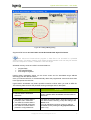
ingenia dsPIC bootloader
User’s Guide
version 1.1
03/02/06
© 2005, ingenia-cat S.L.
ingenia dsPIC bootloader Guide: V1.1
Copyright © 2005 ingenia-cat S.L.
Permission is granted to copy and/or distribute this document under the terms of the GNU Free
Documentation License,
Microchip, MPLAB and dsPIC are registered trademarks of Microchip Technology Incorporated
in the U.S.A. and other countries.
Content
1
Getting started............................................................................................ 2
2
ingenia dsPIC bootloader .......................................................................... 3
2.1 ingenia dsPIC bootloader firmware .................................................... 3
2.1.1 Requisites......................................................................................... 3
2.1.2 How it works? ................................................................................... 4
2.1.3 Communication Protocol Description................................................ 4
2.1.3.1 Synchronization ............................................................................. 5
2.1.3.2 Commands .................................................................................... 5
2.1.3.2.1Firmware version command ..................................................... 5
2.1.3.2.2Read command ........................................................................ 5
2.1.3.2.3Write command ........................................................................ 5
2.1.3.2.4User Program command .......................................................... 6
2.1.3.2.5Unknown command.................................................................. 6
2.1.4 How to use it with another dsPIC30F ............................................... 7
2.1.5 Limitations ........................................................................................ 8
2.2 ingenia dsPIC bootloader Graphic User Interface ........................... 10
2.2.1 Requisites....................................................................................... 10
2.2.2 Setting up the Hardware................................................................. 10
2.2.2.1 Starting ingenia dsPIC bootloader ............................................... 10
2.2.2.2 Setting up the port and the baud rate .......................................... 11
2.2.2.3 Detecting the dsPIC..................................................................... 11
2.2.3 Loading and Writing programs ....................................................... 11
2.2.4 The XML dsPIC list file ................................................................... 13
2.2.4.1 Adding a new device ................................................................... 13
2.2.4.2 Protecting zones of your dsPIC ................................................... 14
3
ingenia bootloader Source Code ............................................................ 15
4
dsPIC list file for iCM4011........................................................................ 19
5
References ................................................................................................ 20
6
Revision History ....................................................................................... 21
ingenia dsPIC boot loader – User Guide
1
Getting started
A serial bootloader is a firmware (software embedded in a hardware device) located into
the non-volatile memory of a Microcontroller Unit (MCU) that allows in-circuit
reprogramming of the device using its standard communication ports.
Usually, the process to program a MCU implies the need of an expensive hardware device.
Such devices, also called programmers, use the special purpose pins of the MCUs to access to
the internal memory. Modifying the voltage applied to these pins, a read or write cycle of the
memory could be performed.
Moreover, the programmers also should incorporate a serial interface in order to allow the
communications with the sender device (normally a Personal Computer (PC)). Together with the
hardware programmer, comes software that helps the final user to send his own firmware
through the serial port of the PC to the MCU.
In the other hand, a serial bootloader is just a piece of code that works with the communication
ports of an MCU and takes advantage of the capacity to write into his own non-volatile memory.
This means that hardware programmer must be used at least once to load it into the MCU.
Then, the user can reprogram the MCU as many times as required without the need of the
hardware programmer.
One of the main advantages of using a serial bootloader in a hardware device that contains a
firmware, is that adds to it the capacity to be easily upgradeable (the user just needs a PC to
update the firmware version). This procedure will save the cost of disassemble and send the
device back to the factory.
[email protected] | www.ingenia-cat.com
2
ingenia dsPIC boot loader – User Guide
2
ingenia dsPIC bootloader
ingenia has developed a serial bootloader package specially focused on the dsPIC30F family of
Microchip and tested with ingenia Communication Module (iCM4011).
Mainly the bootloader package is divided into two parts:
•
•
2.1
An open source firmware code (iBL) and,
A Windows based Graphical User Interface.
ingenia dsPIC bootloader firmware
As explained above, the firmware must be loaded into the MCU using a hardware programmer.
ingenia offers a variety of development kits based on dsPIC30F which come with the
bootloader already programmed inside such as iCM4011. Contact ingenia for further
information.
The main features of ingenia’s bootloader firmware are:
•
•
•
•
•
Auto-Baud rate detection – The bootloader has the ability to adjust its own baud rate
to the one used by the sender by mean of a synchronization protocol.
Possibility of Read and Write Program (Flash) Memory – The bootloader is able to
access to the whole non-volatile memory dedicated to program code.
Possibility of Read and Write EEPROM Memory - The bootloader is able to access to
the whole non-volatile memory dedicated to data.
Possibility of Read and Write Configuration Registers - The bootloader is able to
access to the configuration registers zone.
Optimized assembler code – The firmware is implemented minimizing the used code
size.
2.1.1 Requisites
The system requirements to use ingenia bootloader package is shown in the Figure 1.
This system is composed by the following elements:
•
•
•
A personal computer with ingenia dsPIC bootloader Graphic User Interface installed.
See 2.2.
A dsPIC30F Board with the Firmware already loaded it and with a communications
transceiver (i.e. iCM4011).
The appropriate communication cable (USB, RS232, etc) according to the used
transceiver.
Figure 1: Typical System
[email protected] | www.ingenia-cat.com
3
ingenia dsPIC boot loader – User Guide
2.1.2 How it works?
Conceptually the firmware can be seen as a flow of states (see Figure 2). Below there is a
description of them and the conditions necessary to move from one to another.
•
•
•
•
•
•
•
Reset – When a power-up or a reset occurs the dsPIC* enters in this state and jumps
directly to the Baud Rate Detection.
Baud rate detection – In this state, synchronization with the sender is performed in
order to compute the used baud rate. After a time (one second if 7.3728 MHz crystal
is used) if no synchronization is established a timeout occurs and the execution goes
to the User program. If the baud rate is detected correctly the execution continues in
the Wait Commands state.
Wait Commands – During this state the dsPIC listens continuously the UART port. If
a known command is received, the program will jump to the corresponding state
(version, read, write, or user program). Otherwise will stay in this state indefinitely.
Version – The version of the Firmware is sent through the UART and the execution
returns to Wait Commands state.
Read – A read memory operation is realized, the result is sent through the UART and
the execution returns to Wait Commands state.
Write – A write memory operation is realized and the execution returns to Wait
Commands state.
User Program – The program execution jumps to starting user program address
(0x100) and therefore the bootloader ends.
Figure 2: Flow State Diagram of the bootloader
2.1.3 Communication Protocol Description
As explained in 2.1.2 the firmware is composed by a set of states that can be grouped into:
•
•
Baud rate detection or synchronization between the two devices and
Commands
Following there is a detailed explanation of the functionality of each group.
[email protected] | www.ingenia-cat.com
4
ingenia dsPIC boot loader – User Guide
2.1.3.1
Synchronization
In order to achieve a correct synchronization, the remote device should send continuously the
ASCII character ‘U’ (0x55) to the dsPIC. The representation of this character in binary is
01010101b giving the maximum frequency of transitions in a fixed baud rate (See
Figure 3).
Figure 3: Representation of the character 0x55
When the bootloader detects the first rising edge, starts a timer and looks for the next four rising
edges. Once is detected the last edge one, the timer is stopped and the baud rate computed by
means of a simple division.
2.1.3.2
Commands
The frame of all the commands used by the bootloader starts with an Identification Byte. The
answer frame is always ended with acknowledge (ACK = 0x55) or non-acknowledge (NACK =
0xFF) but the Reset command.
2.1.3.2.1
Firmware version command
Check the major and minor version of the firmware.
Command:
Answer:
2.1.3.2.2
Read command
Read the content of a position of the memory, which could be FLASH, EEPROM or Configure
registers addressed by a 24bits word. The answer is also a 24bits data Word.
Command:
Answer:
2.1.3.2.3
Write command
Carries out a write memory operation, which could be FLASH, EEPROM or Configure registers.
The writing operation is done in row mode access (See 2.1.5 for further information), thus you
should specify the initial address, the length of the row and the whole row content.
The frame ends with a CRC that is computed as the 256 module of all the data value addition.
[email protected] | www.ingenia-cat.com
5
ingenia dsPIC boot loader – User Guide
Command:
Answer:
or
2.1.3.2.4
User Program command
Force the user program execution, which should be located at address 0x100.
Command:
Answer: None
2.1.3.2.5
Unknown command
When an unknown command is received the bootloader sends a non-acknowledge.
Answer:
[email protected] | www.ingenia-cat.com
6
ingenia dsPIC boot loader – User Guide
RESET
no
BDR
received
from UART?
no
Timeout
yes
yes
Compute Baudrate
and configure UART
USER
CODE
dsPIC sends
ACK
yes
no
BYTE
received
from UART?
yes
User
program
command?
no
Version
command?
no
Read
command?
no
Write
command?
no
dsPIC sends
firmware version
Receive
address
Receive Frame
(address + N + data
+ CRC)
dsPIC sends
memory content
CRC OK?
no
dsPIC sends
NACK
Assigns Erase/Write Row
code and number of latches
depending on memory region
Erase Row (except if
Config register)
Load latches
dsPIC sends
ACK
Write Row
Figure 4: More detailed flowchart of the bootloader
2.1.4 How to use it with another dsPIC30F
The serial bootloader package comes with both, a MPLAB* project and a compiled version of
the assembler file valid for the dsPIC30F4011.
However, if you want to use the firmware with another dsPIC30F family device you should
change the project and recompile it.
These are the steps to follow:
1.
2.
Start MPLAB and open the iBL.mcp project.
In the option Select Device of the menu Configure, select the device of your system.
(see Figure 5).
[email protected] | www.ingenia-cat.com
7
ingenia dsPIC boot loader – User Guide
Figure 5: Selection of the device
3.
4.
5.
In the project window remove the default linker script (p30f4011.gld) and add the
corresponding to your device (See
Figure 6).
After that you should be able to recompile the project normally.
Figure 6: Modifying the linker script
2.1.5 Limitations
The bootloader firmware uses by default the alternate UART pins. If you want to use the main
UART pins you should replace the initialization as follows:
[email protected] | www.ingenia-cat.com
8
ingenia dsPIC boot loader – User Guide
; Uart init
mov #0x8420, W0
mov W0, U1MODE
; W0 = 0x8420 -> 1000 0100 0010 0000b
; Enable UART with Alternate IO, Auto Baud and 8N1
by
; Uart init
mov #0x8020, W0
mov W0, U1MODE
; W0 = 0x8020 -> 1000 0000 0010 0000b
; Enable UART with Main IO, Auto Baud and 8N1
The writing of the EEPROM and Flash memories uses only the row mode access. Internally,
the firmware erases and writes a whole row. Thus, to perform a correct writing operation the
sender must:
1. Ensure the initial address of writing match an initial row position,
2. Send the data corresponding to the whole row.
[email protected] | www.ingenia-cat.com
9
ingenia dsPIC boot loader – User Guide
2.2
ingenia dsPIC bootloader Graphic User Interface
ingenia dsPIC bootloader is a graphic user interface that allows loading a program into a dsPIC,
by using iBL (ingenia bootloader) firmware open source and an appropriate hardware platform
(such as iCM).
The following diagram shows this architecture:
Figure 7: architecture for using ingenia dsPIC bootloader
2.2.1 Requisites
Minimum recommended system requirements for ingenia dsPIC bootloader Graphic User
Interface are:
9
9
9
CPU: Intel Pentium II (366 MHz or higher) with serial port for programming (USB also
available if using iCM4011)
Memory: 64 MB minimum
Operating System: Windows 2000/XP
2.2.2 Setting up the Hardware
2.2.2.1
Starting ingenia dsPIC bootloader
When you start ingenia dsPIC bootloader software, a message pops up alerting you to
shutdown your hardware platform (i.e. iCM4011) before start detection process (
Figure 8). You must do this for synchronization reasons between the bootloader firmware saved
into the dsPIC and this software.
Figure 8: Starting ingenia dsPIC bootloader
Click on the ‘OK, my platform is shut down’ button when your platform is completely shut down.
[email protected] | www.ingenia-cat.com
10
ingenia dsPIC boot loader – User Guide
Check the ‘don’t remember me again’ option if you don’t want to be alerted next time you
run ingenia dsPIC bootloader.
2.2.2.2
Setting up the port and the baud rate
Before start the detection process of the dsPIC and bootloader firmware, you will have to select
the COM port where you will plug your dsPIC platform and the baud rate to use for transferring
data. The maximum allowed baud rate is 115200bps.
If you are working on a noisy electric environment or your serial cable is long (> 5mts), you may
want to select a slower baud rate for transferring data.
2.2.2.3
Detecting the dsPIC
Once you have configured your COM, you can start the detection process of dsPIC and
bootloader firmware. A message appears (Figure 9) asking you to start your dsPIC platform.
Figure 9: Detecting the dsPIC
Few seconds after you start your platform, if the process succeeds, a message will pop up
identifying the dsPIC detected and its bootloader firmware version.
If the detection process fails, restart the process making sure that your platform is shut down
before detection process starts.
If problems persist, contact ingenia at [email protected] or send us an incidence at:
http://www.ingenia-cat.com/soportecnic.php.
2.2.3 Loading and Writing programs
When you finish the detection process, you can load as many files as you want into your dsPIC.
The loading & writing dialog window pops up (Figure 10).
Do not shut down your platform while loading and writing programs. If you do that, the
results could be unexpected and you will have to restart the above process.
To load a file, click on the folder button and browse until getting it.
[email protected] | www.ingenia-cat.com
11
ingenia dsPIC boot loader – User Guide
Click and browse
for an HEX file
Writeable memory
zones of dsPIC
Figure 10: Loading & Writing Dialog
Supported file formats are Intel 16-bit and 32-bit hexadecimal object file format.
Intel's Hex-record format allows program or data files to be encoded in a printable
(ASCII) format. This allows viewing of the object file with standard tools and easy file transfer
from one computer to another, or between a host and target.
Writeable memory zones of a dsPIC can be divided into:
•
•
•
program flash
write data EEPROM
and configure registers
ingenia dsPIC bootloader shows you the three zones and its associated range address
accordingly with the detected dsPIC.
Once you load the HEX file, it will automatically detect the programmed zones and check them
in the appropriate check boxes.
ingenia dsPIC bootloader may detect possible overwrite conflicts when you load an HEX file.
The following table resumes the possible warning messages and its description
Message
Description
• code has data in bootloader
addresses
The HEX contains data in bootloader reserved
region. ingenia dsPIC bootloader will never write on
this zone.
• Your HEX file contains data in
protected 'code' addresses
• Your HEX file contains data in
protected ‘EPROM’ addresses
• Your HEX file contains data in
protected ‘config’ addresses
The HEX file contains data in protected regions. You
can either omit the warning, or skip the writing of the
whole zone.
You can add protect regions of memory within a
writeable zone by editing the ibl_dspiclist.xml file
(see 2.2.4).
[email protected] | www.ingenia-cat.com
12
ingenia dsPIC boot loader – User Guide
Once you have loaded the file you can start the write process by clicking on the ‘start write’
button.
A progress bar appears showing the write progress. If the write succeeds, the grey button
displayed on the bottom of the dialog, becomes green. Otherwise, becomes red and an error
message will pops up.
2.2.4 The XML dsPIC list file
ingenia dsPIC bootloader can work with dsPIC30F family Digital Signal Controllers (for instance
iCM works with dsPIC30F4011). The detection process of dsPIC (see 2.2.2.3), uses
ibl_dspiclist.xml file to identify the controller and its features. This file is located in the
installation folder and consists in a list of supported dsPICs (or devices).
If the dsPIC that uses your platform doesn’t appear in that list, you can add them obeying the
XML syntax used in the file. Next section will help you to do that. A DTD enclosed with the XML
file will also help you check your XML syntax.
For further information on writing XML files refer to http://www.w3.org/XML/ .
A DTD ("Document Type Definition) is a set of declarations that conform to a particular
markup syntax and that describe a class, or "type", of SGML or XML documents, in terms of
constraints on the structure of those documents.
2.2.4.1
Adding a new device
Each dsPIC is named as a device in the XML dsPIC list file. A device is a description of a
dsPIC. They are characterized by an id and a name. The id is the Microchip device ID (DEVID),
and the name is the Microchip device name.
Within tags <device></device> you have to define three memory zones:
•
•
•
code or programming,
data,
and configuration
Code zone is represented with <memcode> tag.
Data zone is represented with <memdata> tag.
And configuration zone is represented with <memconfig> tag.
In each zone you need to define its start address and end address as an attributes of the tag.
Also within memcode zones you have to specify bootloader region by using <bootloader> tag.
The bootloader region defines the zone where bootloader is located. This zone will be protected
against overwrites, so be sure to define its start and end address properly (you will never be
able to write code in this region).
The XML dsPIC list file comes with bootloader region defined for iCM. If you are using a
different platform, change it accordingly.
The following example shows a complete definition of a device.
[email protected] | www.ingenia-cat.com
13
ingenia dsPIC boot loader – User Guide
<device id="0x0101" name="dsPIC4011">
<memcode startaddress="0x000000" endaddress="0x007FFE">
<boot loader startaddress="0x007EC0" endaddress="0x007FFE"/>
</memcode>
<memdata startaddress="0x7FFC00" endaddress="0x7FFFFE"/>
<memconfig startaddress="0xF80000" endaddress="0xF8000B">
</memconfig>
</device>
2.2.4.2
Protecting zones of your dsPIC
You can protect from overwriting memory regions of your dsPIC by using <protected> tag within
a memory zone.
To do that, specify the startaddress and the endaddress of the protected zone in the attributes
of <protected> tag.
The following example protects the memory region starting at 0xF8000A and ending at
0xF8000B in the configuration zone.
<memconfig startaddress="0xF80000" endaddress="0xF8000B">
<protected startaddress="0xF8000A" endaddress="0xF8000B"/>
</memconfig>
You can protect as many regions as you want.
If you try to write code on those regions, ingenia dsPIC bootloader will alert you about that and
you will decide whether to proceed or not.
See section 4 for a complete example of an XML dsPIC list file.
[email protected] | www.ingenia-cat.com
14
ingenia dsPIC boot loader – User Guide
3
ingenia bootloader Source Code
;******************************************************************************
;*
*
;* Project:
ingenia BootLoader
*
;* Module:
iBL.s
*
;* Description: dsPic bootloader with autobaud detection
*
;*
Read/Write through UART: PGM, EEPROM & Config registers
*
;* Author:
Roger Juanpere
*
;*
*
;* Revision: 1.0 (17-08-05): Initial version
*
;*
1.1 (01-02-06): Added support for >32K PGM devices
*
;*
*
;******************************************************************************
;* ingenia-cat S.L. (c)
www.ingenia-cat.com
*
;******************************************************************************
.include "p30fxxxx.inc"
;******************************************************************************
; Configuration bits:
;******************************************************************************
config __FOSC, CSW_FSCM_OFF & EC_PLL16
;Turn off clock switching and
;fail-safe clock monitoring and
;use the External Clock as the
;system clock
config __FWDT, WDT_OFF
;Turn off Watchdog Timer
config __FBORPOR, PBOR_ON & BORV_27 & PWRT_16 & MCLR_EN
;Set Brown-out Reset voltage and
;and set Power-up Timer to 16msecs
config __FGS, CODE_PROT_OFF
;Set Code Protection Off for the
;General Segment
;******************************************************************************
; Program Specific Constants (literals used in code)
;******************************************************************************
.equ CRC, W4
.equ ACK, 0x55
.equ NACK, 0xFF
.equ USER_ADDRESS, 0x0100
.equ START_ADDRESS, 0x7D00
; Relative to 0x0100
.equ CFG_M, 0xF8
.equ EE_M, 0x7F
.equ
.equ
.equ
.equ
.equ
C_READ, 0x01
C_WRITE, 0x02
C_VERSION, 0x03
C_USER, 0x0F
MAX_WORD_ROW, 64
.equ MAJOR_VERSION, 0x01
.equ MINOR_VERSION, 0x01
;******************************************************************************
; Global Declarations:
;******************************************************************************
.global __reset
;The label for the first line of code.
.global recBuf
;******************************************************************************
;Uninitialized variables in X-space in data memory
;******************************************************************************
.section bss, xmemory
recBuf:
.space 2 * MAX_WORD_ROW
;******************************************************************************
;Code Section in Program Memory
;******************************************************************************
.text
; Start of Code section
[email protected] | www.ingenia-cat.com
15
ingenia dsPIC boot loader – User Guide
.org #START_ADDRESS
__reset:
MOV #__SP_init, W15
MOV #__SPLIM_init, W0
MOV W0, SPLIM
NOP
; Uart init
mov #0x8420, W0
mov W0, U1MODE
clr U1STA
; Initialize the Stack Pointer
; Initialize the Stack Pointer Limit Register
; Add NOP to follow SPLIM initialization
; W0 = 0x8420 -> 1000 0100 0010 0000b
; Enable UART with Alternate IO, AutoBaud and 8N1
; Timer 3 init
clr T3CON
bclr IEC0, #T3IE
setm PR3
mov #0x8000, W0
set to internal cycle
mov W0, T3CON
; Input Capture init
clr IC1CON
bset IC1CON, #1
bclr IFS0, #IC1IF
bclr IEC0, #IC1IE
;
;
;
;
Stops any 16-bit Timer3 operation
Disable Timer 3 interrupt
Set Timer 3 period to maximum value 0xFFFF
Start Timer 3 with 1:1 prescaler and clock source
;
;
;
;
Turn off Input Capture 1 module
Input Capture Mode every risind edge
Clear Input Capture flag
Disable Input Capture interrupts
; Start Autobaud detection
mov #0x0004, W0
; W0 = 0x0004
rcall WaitRising
; Wait until the first Rising edge is detected
clr TMR3
; Clear content of the Timer 3 timer register
ByteLoop:
rcall WaitRising
dec W0, W0
; W0-bra NZ, ByteLoop
; if W0 != 0 jump to ByteLoop
bclr T3CON, #TON
; Last Rising edge detected so Stop Timer 3
mov TMR3, W0
; W0 = TMR3
add #0x40, W0
; For rounding: +64 >> 7 is equal to +0.5
asr W0, #7, W0
; W0 = ((Tend - Tini + 64) / 128)
dec W0, W0
; W0-; Uart re-init
mov W0, U1BRG
; U1BRG = W0 -> Configs UART with the detected
baudrate
bclr U1MODE, #ABAUD
bset U1STA, #UTXEN
bra SendAck
StartFrame:
btss U1STA, #URXDA
bra StartFrame
mov U1RXREG, W0
cp.b W0, #C_USER
btsc SR, #Z
goto USER_ADDRESS
cp.b W0, #C_READ
bra Z, ReadMemCmd
cp.b W0, #C_WRITE
bra Z, WriteMemCmd
cp.b W0, #C_VERSION
bra Z, VersionCmd
bra SendNack
VersionCmd:
mov
mov
mov
mov
bra
#MAJOR_VERSION, W0
W0, U1TXREG
#MINOR_VERSION, W0
W0, U1TXREG
SendAck
ReadMemCmd:
rcall ReceiveChar
mov W0, TBLPAG
rcall ReceiveChar
swap W0
rcall ReceiveChar
tblrdh [W0], W1
; Disable AutoBaud
; Enable transmition
; Wait until a character is received
; Compare received Character with USER character
; Compare received Character with READ character
; Compare received Character with WRITE character
; Compare received Character with VERSION character
; Unknown character -> Send NACK
; Send Major Version
; Send Minor Version
; Receive high byte of the address
; High address byte
; Receive medium byte of the address
; Receive low byte of the address
; Read high word to W1
[email protected] | www.ingenia-cat.com
16
ingenia dsPIC boot loader – User Guide
mov W1, U1TXREG
; Send W1 low byte
tblrdl [W0], W1
swap W1
mov W1, U1TXREG
swap W1
mov W1, U1TXREG
; Read low word to W1
; Send W1 high byte
; Send W1 low byte
SendAck:
mov
bra
SendNack:
mov
Send:
mov
bra
#ACK, W0
Send
; Send an ACK character
#NACK, W0
; Send a KO character
W0, U1TXREG
StartFrame
WriteMemCmd:
clr W4
rcall ReceiveChar
mov W0, TBLPAG
mov W0, NVMADRU
TBLPAG
rcall ReceiveChar
mov.b WREG, NVMADR + 1
rcall ReceiveChar
mov.b WREG, NVMADR
rcall ReceiveChar
mov W0, W3
mov #recBuf, W2
FillBufLoop:
rcall ReceiveChar
mov.b W0, [W2++]
dec W3, W3
bra nz, FillBufLoop
;
;
;
;
Reset W4 = Checkbyte
Receive high byte of the initial address
For latch loading and programming
For erase cycle - in program are written auto. from
; Receive medium byte of the initial address
; Receive low byte of the initial address
; Receive the number of bytes to be received
; W2 = recBuf
; Move received byte to recBuf
; Fill reception buffer
cp0.b W4
bra nz, SendNack
mov #recBuf, W2
mov NVMADR, W5
;
;
;
;
mov #CFG_M, W0
cp.b TBLPAG
bra nz, noCFM
; Check if destination is Config Memory
mov #0x4008, W8
need to be erased
mov #1, W3
bra LoadLatch
noCFM:
mov #EE_M, W0
cp.b TBLPAG
bra NZ, noEEM
mov #0x4075, W0
mov #0x4005, W8
mov #32, W3
bra StartWritingCycle
noEEM:
mov #0x4071, W0
mov #0x4001, W8
mov #64, W3
64word16)
StartWritingCycle:
rcall WriteKey
LoadLatch:
tblwtl [W2++], [W5]
dec W3, W3
bra Z, EndLatch
tblwth [W2++], [W5++]
dec W3, W3
bra NZ, LoadLatch
EndLatch:
mov W8, W0
rcall WriteKey
bra SendAck
Check (INTEL HEX8 Checksum - Sum modulo 256)
if Checkbyte != 0 jump to SendNack
W2 = recBuf
Use W5 as low word address
; Assigns Write Config Row Code - Config Mem doesn't
; Assigns Number of 16bits words per Row
; Check if destination is EEPROM Memory
;
;
;
;
Assigns Erase EEPROM Row Code
Assigns Write EEPROM Row Code
Assigns Number of 16bits word per Row
Erase and Write Memory
; Assigns Erase PGM Row Code
; Assigns Write PGM Row Code
; Assigns Number of 16bits word per Row (32instr -
; Erase selected Row
; Load low word to latch
; Load high word to latch
; Repeat until whole row is loaded
; Write selected Row
; Send an ACK character
[email protected] | www.ingenia-cat.com
17
ingenia dsPIC boot loader – User Guide
;******************************************************************************
;Procedures
;******************************************************************************
WaitRising:
mov #0x5A, W2
; W2 = 0x5A
MajorLRise:
setm W1
; W1 = 0xFFFF
MinorLRise:
btsc IFS0, #IC1IF
; Rising edge detected?
bra EndRising
; Yes -> Jump to finish detection
dec W1, W1
; W1-bra NZ, MinorLRise
; if W1 != 0 jump MinorLRise
dec W2, W2
; W2-bra NZ, MajorLRise
; if W2 != 0 jump MajorLRise
goto USER_ADDRESS
; Timeout aprox. = 0x5A * 0xFFFF * 5 clocks -> Jump to
user soft
EndRising:
bclr IFS0, #IC1IF
return
; Clear Interrupt Flag
;******************************************************************************
ReceiveChar:
mov #0xFFFF, W10
; W10 = 0xFFFF
MajorLChar:
setm W11
; W11 = 0xFFFF
MinorLChar:
btsc U1STA, #URXDA
; Character received ?
bra EndReceiveChar
; Yes -> Jump to Finish reception
dec W11, W11
; W1-bra NZ, MinorLChar
; if W1 != 0 jump MinorLChar
dec W10, W10
; W2-bra NZ, MajorLChar
; if W2 != 0 jump MajorLChar
MOV #__SP_init, W15
; Initialize Stack Pointer
bra SendNack
; Timeout aprox. = 0xFFFF * 0xFFFF * 5 clocks -> Jump
to Send Nack
EndReceiveChar:
mov.b U1RXREG, WREG
; W0 = U1RXREG
add.b W4, W0, W4
; Checkbyte += W0 -> Performs a Sum modulo 256
checksum (INTEL HEX8)
return
;******************************************************************************
WriteKey:
mov W0, NVMCON
mov #0x55, W0
mov W0, NVMKEY
mov #0xAA, W0
mov W0, NVMKEY
bset NVMCON, #WR
; Start Writing
nop
nop
WaitWriting:
btsc NVMCON, #WR
; WR or WREN - Wait until operation is finished
bra WaitWriting
return
;--------End of All Code Sections --------------------------------------------.end
; End of program code in this file
[email protected] | www.ingenia-cat.com
18
ingenia dsPIC boot loader – User Guide
4
dsPIC list file for iCM4011
<?xml version="1.0" encoding="iso-8859-1"?>
<!DOCTYPE devices SYSTEM "ingeniadspicbootloader.dtd">
<devices>
<device id="0x01C1" name="dsPIC3011">
<memcode startaddress="0x000000" endaddress="0x003FFE">
<bootloader startaddress="0x003E00" endaddress="0x003FFE"/>
</memcode>
<memdata startaddress="0x7FFC00" endaddress="0x7FFFFE"/>
<memconfig startaddress="0xF80000" endaddress="0xF8000B">
<protected startaddress="0xF8000A" endaddress="0xF8000B"/>
</memconfig>
</device>
<device id="0x0101" name="dsPIC4011">
<memcode startaddress="0x000000" endaddress="0x007FFE">
<bootloader startaddress="0x007E00" endaddress="0x007FFE"/>
</memcode>
<memdata startaddress="0x7FFC00" endaddress="0x7FFFFE"/>
<memconfig startaddress="0xF80000" endaddress="0xF8000B">
<protected startaddress="0xF8000A" endaddress="0xF8000B"/>
</memconfig>
</device>
<device id="0x0080" name="dsPIC5011">
<memcode startaddress="0x000000" endaddress="0x00AFFE">
<bootloader startaddress="0x00AE00" endaddress="0x00AFFE"/>
</memcode>
<memdata startaddress="0x7FFC00" endaddress="0x7FFFFE"/>
<memconfig startaddress="0xF80000" endaddress="0xF8000B">
<protected startaddress="0xF8000A" endaddress="0xF8000B"/>
</memconfig>
</device>
<device id="0x0198" name="dsPIC6014">
<memcode startaddress="0x000000" endaddress="0x017FFE">
<bootloader startaddress="0x017E00" endaddress="0x017FFE"/>
</memcode>
<memdata startaddress="0x7FF000" endaddress="0x7FFFFE"/>
<memconfig startaddress="0xF80000" endaddress="0xF8000B">
<protected startaddress="0xF8000A" endaddress="0xF8000B"/>
</memconfig>
</device>
</devices>
[email protected] | www.ingenia-cat.com
19
ingenia dsPIC boot loader – User Guide
5
-
References
“dsPIC30F Family Reference Manual” from Microchip Technology Inc (DS70046).
“dsPIC30F Flash Programming Specification” from Microchip Technology Inc. (DS70102).
“dsPIC30F/33F Programmer’s Reference Manual” from Microchip Technology Inc.
(DS70157)
“iCM4011 Product Manual” from ingenia-cat S.L.
[email protected] | www.ingenia-cat.com
20
ingenia dsPIC boot loader – User Guide
6
Revision History
Comments
Date
Release
First Release
01/12/2005
1.0
Style document revision
Updated ingenia bootloader Souce Code
Updated dsPIC list file for iCM4011
03/02/2005
1.1
[email protected] | www.ingenia-cat.com
21