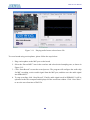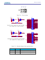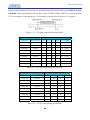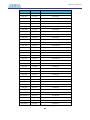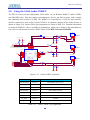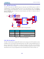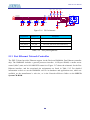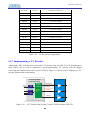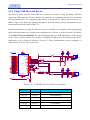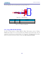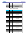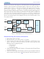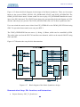
1
Altera DE2-70 Board Version 1.03 Copyright © 2008 Terasic Technologies Altera DE2-70 Board CONTENTS Chapter 1 DE2-70 Package ...............................................................................................................1 1.1 1.2 1.3 Package Contents .................................................................................................................1 The DE2-70 Board Assembly ..............................................................................................2 Getting Help.........................................................................................................................3 Chapter 2 Altera DE2-70 Board .......................................................................................................4 2.1 2.2 2.3 Layout and Components ......................................................................................................4 Block Diagram of the DE2-70 Board ..................................................................................5 Power-up the DE2-70 Board................................................................................................9 Chapter 3 DE2-70 Control Panel.................................................................................................... 11 3.1 3.2 3.3 3.4 3.5 3.6 3.7 3.8 3.9 Control Panel Setup ........................................................................................................... 11 Controlling the LEDs, 7-Segment Displays and LCD Display .........................................13 Switches and Buttons .........................................................................................................15 SDRAM/SSRAM/Flash Controller and Programmer........................................................16 USB Monitoring.................................................................................................................18 PS2 Device.........................................................................................................................19 SD CARD ..........................................................................................................................20 Audio Playing and Recording ............................................................................................21 Overall Structure of the DE2-70 Control Panel .................................................................23 Chapter 4 DE2-70 Video Utility......................................................................................................25 4.1 4.2 4.3 4.4 Video Utility Setup.............................................................................................................25 VGA Display......................................................................................................................26 Video Capture ....................................................................................................................27 Overall Structure of the DE2-70 Video Utility ..................................................................28 Chapter 5 Using the DE2-70 Board................................................................................................30 5.1 5.2 5.3 5.4 5.5 5.6 5.7 5.8 5.9 5.10 5.11 Configuring the Cyclone II FPGA .....................................................................................30 Using the LEDs and Switches............................................................................................32 Using the 7-segment Displays............................................................................................36 Clock Circuitry...................................................................................................................38 Using the LCD Module......................................................................................................40 Using the Expansion Header..............................................................................................41 Using VGA ........................................................................................................................45 Using the 24-bit Audio CODEC ........................................................................................48 RS-232 Serial Port .............................................................................................................49 PS/2 Serial Port ..................................................................................................................49 Fast Ethernet Network Controller ......................................................................................50 ii Altera DE2-70 Board 5.12 5.13 5.14 5.15 5.16 TV Decoder........................................................................................................................52 Implementing a TV Encoder..............................................................................................54 Using USB Host and Device..............................................................................................55 Using IrDA.........................................................................................................................56 Using SDRAM/SRAM/Flash.............................................................................................57 Chapter 6 Examples of Advanced Demonstrations ......................................................................66 6.1 6.2 6.3 6.4 6.5 6.6 6.7 6.8 6.9 6.10 DE2-70 Factory Configuration ..........................................................................................66 TV Box Demonstration......................................................................................................67 TV Box Picture in Picture (PIP) Demonstration................................................................69 USB Paintbrush..................................................................................................................72 USB Device........................................................................................................................74 A Karaoke Machine ...........................................................................................................76 Ethernet Packet Sending/Receiving ...................................................................................78 SD Card Music Player........................................................................................................80 Music Synthesizer Demonstration .....................................................................................83 Audio Recording and Playing ............................................................................................87 Chapter 7 Appendix .........................................................................................................................90 7.1 7.2 Revision History ................................................................................................................90 Copyright Statement ..........................................................................................................90 iii DE2-70 User Manual Chapter 1 DE2-70 Package The DE2-70 package contains all components needed to use the DE2-70 board in conjunction with a computer that runs the Microsoft Windows software. 1.1 Package Contents Figure 1.1 shows a photograph of the DE2-70 package. Figure 1.1. The DE2-70 package contents. 1 DE2-70 User Manual The DE2-70 package includes: The DE2-70 board USB Cable for FPGA programming and control DE2-70 System CD containing the DE2-70 documentation and supporting materials, including the User Manual, the Control Panel utility, reference designs and demonstrations, device datasheets, tutorials, and a set of laboratory exercises CD-ROMs containing Altera’s Quartus® II Web Edition and the Nios® II Embedded Design Suit Evaluation Edition software. Bag of six rubber (silicon) covers for the DE2-70 board stands. The bag also contains some extender pins, which can be used to facilitate easier probing with testing equipment of the board’s I/O expansion headers Clear plastic cover for the board 12V DC wall-mount power supply 1.2 The DE2-70 Board Assembly To assemble the included stands for the DE2-70 board: Assemble a rubber (silicon) cover, as shown in Figure 1.2, for each of the six copper stands on the DE2-70 board The clear plastic cover provides extra protection, and is mounted over the top of the board by using additional stands and screws Figure 1.2. The feet for the DE2-70 board. 2 DE2-70 User Manual 1.3 Getting Help Here are the addresses where you can get help if you encounter problems: Altera Corporation 101 Innovation Drive San Jose, California, 95134 USA Email: [email protected] Terasic Technologies No. 356, Sec. 1, Fusing E. Rd. Jhubei City, HsinChu County, Taiwan, 302 Email: [email protected] Web: DE2-70.terasic.com 3 DE2-70 User Manual Chapter 2 Altera DE2-70 Board This chapter presents the features and design characteristics of the DE2-70 board. 2.1 Layout and Components A photograph of the DE2-70 board is shown in Figure 2.1. It depicts the layout of the board and indicates the location of the connectors and key components. Ethernet 10/100M Port USB Device Port USB Blaster Port Mic in USB Host Port Line In Line Out VGA Out RS-232 Port Video In 1 Video In 2 TV Decoder (NTSC/PAL) X2 12V DC Power Supply Connector PS2 Port VGA 10-bit DAC Power ON/OFF Switch Ethernet 10/100M Controller USB Host/Slave Controller Audio CODEC 50Mhz Oscillator Altera USB Blaster Controller chipset Expansion Header 2 Altera EPCS16 Configuration Device Expansion Header 1 RUN/PROG Switch for JTAG/AS Modes SD Card Slot Lock (SD Card Not Included) Altera Cyclone II FPGA with 70K LEs 16x2 LCD Module IrDA Transceiver 7-Segment Displays 8Mbyte Flash Memory 8 Green LEDs 18 Red LEDs SMA Extemal Clock 18 Toggle Switches 32Mbyte SDRAMx2 28Mhz Oscillator 2Mbyte SSRAM 4 Push-button Switches Figure 2.1. The DE2-70 board. The DE2-70 board has many features that allow the user to implement a wide range of designed circuits, from simple circuits to various multimedia projects. The following hardware is provided on the DE2-70 board: Altera Cyclone® II 2C70 FPGA device Altera Serial Configuration device - EPCS16 USB Blaster (on board) for programming and user API control; both JTAG and Active Serial 4 DE2-70 User Manual (AS) programming modes are supported 2-Mbyte SSRAM Two 32-Mbyte SDRAM 8-Mbyte Flash memory SD Card socket 4 pushbutton switches 18 toggle switches 18 red user LEDs 9 green user LEDs 50-MHz oscillator and 28.63-MHz oscillator for clock sources 24-bit CD-quality audio CODEC with line-in, line-out, and microphone-in jacks VGA DAC (10-bit high-speed triple DACs) with VGA-out connector 2 TV Decoder (NTSC/PAL/SECAM) and TV-in connector 10/100 Ethernet Controller with a connector USB Host/Slave Controller with USB type A and type B connectors RS-232 transceiver and 9-pin connector PS/2 mouse/keyboard connector IrDA transceiver 1 SMA connector Two 40-pin Expansion Headers with diode protection In addition to these hardware features, the DE2-70 board has software support for standard I/O interfaces and a control panel facility for accessing various components. Also, software is provided for a number of demonstrations that illustrate the advanced capabilities of the DE2-70 board. In order to use the DE2-70 board, the user has to be familiar with the Quartus II software. The necessary knowledge can be acquired by reading the tutorials Getting Started with Altera’s DE2-70 Board and Quartus II Introduction (which exists in three versions based on the design entry method used, namely Verilog, VHDL or schematic entry). These tutorials are provided in the directory DE2_70_tutorials on the DE2-70 System CD-ROM that accompanies the DE2-70 board and can also be found on Altera’s DE2-70 web pages. 2.2 Block Diagram of the DE2-70 Board Figure 2.2 gives the block diagram of the DE2-70 board. To provide maximum flexibility for the user, all connections are made through the Cyclone II FPGA device. Thus, the user can configure the FPGA to implement any system design. 5 DE2-70 User Manual Figure 2.2. Block diagram of the DE2-70 board. Following is more detailed information about the blocks in Figure 2.2: Cyclone II 2C70 FPGA 68,416 LEs 250 M4K RAM blocks 1,152,000 total RAM bits 150 embedded multipliers 4 PLLs 622 user I/O pins FineLine BGA 896-pin package Serial Configuration device and USB Blaster circuit Altera’s EPCS16 Serial Configuration device On-board USB Blaster for programming and user API control JTAG and AS programming modes are supported 6 DE2-70 User Manual SSRAM 2-Mbyte standard synchronous SRAM Organized as 512K x 36 bits Accessible as memory for the Nios II processor and by the DE2-70 Control Panel SDRAM Two 32-Mbyte Single Data Rate Synchronous Dynamic RAM memory chips Organized as 4M x 16 bits x 4 banks Accessible as memory for the Nios II processor and by the DE2-70 Control Panel Flash memory 8-Mbyte NOR Flash memory Support both byte and word mode access Accessible as memory for the Nios II processor and by the DE2-70 Control Panel SD card socket Provides SPI and 1-bit SD mode for SD Card access Accessible as memory for the Nios II processor with the DE2-70 SD Card Driver Pushbutton switches 4 pushbutton switches Debounced by a Schmitt trigger circuit Normally high; generates one active-low pulse when the switch is pressed Toggle switches 18 toggle switches for user inputs A switch causes logic 0 when in the DOWN (closest to the edge of the DE2-70 board) position and logic 1 when in the UP position Clock inputs 50-MHz oscillator 28.63-MHz oscillator SMA external clock input 7 DE2-70 User Manual Audio CODEC Wolfson WM8731 24-bit sigma-delta audio CODEC Line-level input, line-level output, and microphone input jacks Sampling frequency: 8 to 96 KHz Applications for MP3 players and recorders, PDAs, smart phones, voice recorders, etc. VGA output Uses the ADV7123 140-MHz triple 10-bit high-speed video DAC With 15-pin high-density D-sub connector Supports up to 1600 x 1200 at 100-Hz refresh rate Can be used with the Cyclone II FPGA to implement a high-performance TV Encoder NTSC/PAL/ SECAM TV decoder circuit Uses two ADV7180 Multi-format SDTV Video Decoders Supports worldwide NTSC/PAL/SECAM color demodulation One 10-bit ADC, 4X over-sampling for CVBS Supports Composite Video (CVBS) RCA jack input Supports digital output formats : 8-bit ITU-R BT.656 YCrCb 4:2:2 output + HS, VS, and FIELD Applications: DVD recorders, LCD TV, Set-top boxes, Digital TV, Portable video devices, and TV PIP (picture in picture) display. 10/100 Ethernet controller Integrated MAC and PHY with a general processor interface Supports 100Base-T and 10Base-T applications Supports full-duplex operation at 10 Mb/s and 100 Mb/s, with auto-MDIX Fully compliant with the IEEE 802.3u Specification Supports IP/TCP/UDP checksum generation and checking Supports back-pressure mode for half-duplex mode flow control USB Host/Slave controller Complies fully with Universal Serial Bus Specification Rev. 2.0 Supports data transfer at full-speed and low-speed Supports both USB host and device Two USB ports (one type A for a host and one type B for a device) Provides a high-speed parallel interface to most available processors; supports Nios II with a Terasic driver Supports Programmed I/O (PIO) and Direct Memory Access (DMA) 8 DE2-70 User Manual Serial ports One RS-232 port One PS/2 port DB-9 serial connector for the RS-232 port PS/2 connector for connecting a PS2 mouse or keyboard to the DE2-70 board IrDA transceiver Contains a 115.2-kb/s infrared transceiver 32 mA LED drive current Integrated EMI shield IEC825-1 Class 1 eye safe Edge detection input Two 40-pin expansion headers 72 Cyclone II I/O pins, as well as 8 power and ground lines, are brought out to two 40-pin expansion connectors 40-pin header is designed to accept a standard 40-pin ribbon cable used for IDE hard drives Diode and resistor protection is provided 2.3 Power-up the DE2-70 Board The DE2-70 board comes with a preloaded configuration bit stream to demonstrate some features of the board. This bit stream also allows users to see quickly if the board is working properly. To power-up the board perform the following steps: 1. Connect the provided USB cable from the host computer to the USB Blaster connector on the DE2-70 board. For communication between the host and the DE2-70 board, it is necessary to install the Altera USB Blaster driver software. If this driver is not already installed on the host computer, it can be installed as explained in the tutorial Getting Started with Altera's DE2-70 Board. This tutorial is available in the directory 2. 3. 4. 5. 6. DE2_70_tutorials on the DE2-70 System CD-ROM. Connect the 12V adapter to the DE2-70 board Connect a VGA monitor to the VGA port on the DE2-70 board Connect your headset to the Line-out audio port on the DE2-70 board Turn the RUN/PROG switch on the left edge of the DE2-70 board to RUN position; the PROG position is used only for the AS Mode programming Turn the power on by pressing the ON/OFF switch on the DE2-70 board 9 DE2-70 User Manual At this point you should observe the following: All user LEDs are flashing All 7-segment displays are cycling through the numbers 0 to F The LCD display shows Welcome to the Altera DE2-70 The VGA monitor displays the image shown in Figure 2.3. Set the toggle switch SW17 to the DOWN position; you should hear a 1-kHz sound Set the toggle switch SW17 to the UP position and connect the output of an audio player to the Line-in connector on the DE2-70 board; on your headset you should hear the music played from the audio player (MP3, PC, iPod, or the like) You can also connect a microphone to the Microphone-in connector on the DE2-70 board; your voice will be mixed with the music played from the audio player Figure 2.3. The default VGA output pattern. 10 DE2-70 User Manual Chapter 3 DE2-70 Control Panel The DE2-70 board comes with a Control Panel facility that allows users to access various components on the board from a host computer. The host computer communicates with the board through an USB connection. The facility can be used to verify the functionality of components on the board or be used as a debug tool while developing RTL code. This chapter first presents some basic functions of the Control Panel, then describes its structure in block diagram form, and finally describes its capabilities. . 3.1 Control Panel Setup The Control Panel Software Utility is located in the “DE2_70_control_pane/SW” folder in the DE2-70 System CD-ROM. To install it, just copy the whole folder to your host computer. Launch the control panel by executing the “DE2_70_Control_Panel.exe”. Specific control codes should be downloaded to your FPGA board before the control panel can request it to perform required tasks. The control codes include one .sof file and one .elf file. To download the codes, just click the “Download Code” button on the program. The program will call Quartus II and Nios II tools to download the control codes to the FPGA board through USB-Blaster[USB-0] connection. The .sof file is downloaded to FPGA. The .elf file is downloaded to either SDRAM-U2 or SSRAM, according to the user option. To activate the Control Panel, perform the following steps: 1. Make sure Quartus II and NIOS II are installed successfully on your PC. 2. Connect the supplied USB cable to the USB Blaster port, connect the 12V power supply, and turn the power switch ON 3. Set the RUN/PROG switch to the RUN position 4. Start the executable DE2_70_control_panel.exe on the host computer. The Control Panel user interface shown in Figure 3.1 will appear. 5. Select the target memory, SDRAM-U2 or SSRAM, on the control panel. Note. The .elf file will be downloaded to the target memory and the memory will be read-only in later memory access operation. 6. Click Download Code button. Note, the Control Panel will occupy the USB port until you 11 DE2-70 User Manual close that port; you cannot use Quartus II to download a configuration file into the FPGA until you close the USB port. 7. The Control Panel is now ready for use; experiment by setting the value of some LEDs display and observing the result on the DE2-70 board. Figure 3.1. The DE2-70 Control Panel. If you get a "Fail to connect FPGA board" error message on starting the Control Panel program, you can manually download the DE2_70_Control_Panel.sof file using the Quartus Programmer, and then run NiosDownloadBatch.bat. The concept of the DE2-70 Control Panel is illustrated in Figure 3.2. The “Control Codes” that performs the control functions is implemented in the FPGA board. It communicates with the Control Panel window, which is active on the host computer, via the USB Blaster link. The graphical interface is used to issue commands to the control codes. It handles all requests and performs data transfers between the computer and the DE2-70 board. 12 DE2-70 User Manual 7-SEG Display 16x2 LCD USB Blaster SDRAM Flash SSRAM Control Codes PS/2 USB Device SD Card Soket LEDs Figure 3.2. The DE2-70 Control Panel concept. The DE2-70 Control Panel can be used to light up LEDs, change the values displayed on 7-segment and LCD displays, monitor buttons/switches status, read/write the SDRAM, SSRAM and Flash Memory, monitor the status of an USB mouse, read data from a PS/2 keyboard, and read SD-CARD specification information. The feature of reading/writing a word or an entire file from/to the Flash Memory allows the user to develop multimedia applications (Flash Audio Player, Flash Picture Viewer) without worrying about how to build a Memory Programmer. 3.2 Controlling the LEDs, 7-Segment Displays and LCD Display A simple function of the Control Panel is to allow setting the values displayed on LEDs, 7-segment displays, and the LCD character display. Choosing the LED tab leads to the window in Figure 3.3. Here, you can directly turn the individual LEDs on or off by selecting them or click “Light All” or “Unlight All”. 13 DE2-70 User Manual Figure 3.3. Controlling LEDs. Choosing the 7-SEG tab leads to the window in Figure 3.4. In the tab sheet, directly use the Up-Down control and Dot Check box to specified desired patterns, the 7-SEG patterns on the board will be updated immediately. Figure 3.4. Controlling 7-SEG display. 14 DE2-70 User Manual Choosing the LCD tab leads to the window in Figure 3.5. Text can be written to the LCD display by typing it in the LCD box and pressing the Set button. Figure 3.5. Controlling LEDs and the LCD display. The ability to set arbitrary values into simple display devices is not needed in typical design activities. However, it gives the user a simple mechanism for verifying that these devices are functioning correctly in case a malfunction is suspected. Thus, it can be used for troubleshooting purposes. 3.3 Switches and Buttons Choosing the Button tab leads to the window in Figure 3.6. The function is designed to monitor the status of switches and buttons in real time and show the status in a graphical user interface. It can be used to verify the functionality of the switches and buttons. Press the Start button to start button/switch status monitoring process, and button caption is changed from Start to Stop. In the monitoring process, the status of buttons and switches on the board is shown in the GUI window and updated in real time. Press Stop to end the monitoring process. 15 DE2-70 User Manual Figure 3.6. Monitoring switches and buttons. The ability to check the status of button and switch is not needed in typical design activities. However, it provides users a simple mechanism for verifying if the buttons and switches are functioning correctly. Thus, it can be used for troubleshooting purposes. 3.4 SDRAM/SSRAM/Flash Controller and Programmer The Control Panel can be used to write/read data to/from the SDRAM, SSRAM, and FLASH chips on the DE2-70 board. We will describe how the SDRAM-U1 may be accessed; the same approach is used to access the SDRAM-U2, SRAM, and FLASH. Click on the Memory tab and select “SDRAM-U1” to reach the window in Figure 3.7. Please note the target memory chosen for storing .elf file is read-only. Also, please erase the flash before writing data to it. 16 DE2-70 User Manual Figure 3.7. Accessing the SDRAM-U1. A 16-bit word can be written into the SDRAM by entering the address of the desired location, specifying the data to be written, and pressing the Write button. Contents of the location can be read by pressing the Read button. Figure 3.7 depicts the result of writing the hexadecimal value 06CA into location 200, followed by reading the same location. The Sequential Write function of the Control Panel is used to write the contents of a file into the SDRAM as follows: 1. Specify the starting address in the Address box. 2. Specify the number of bytes to be written in the Length box. If the entire file is to be loaded, then a checkmark may be placed in the File Length box instead of giving the number of bytes. 3. To initiate the writing of data, click on the Write a File to Memory button. 4. When the Control Panel responds with the standard Windows dialog box asking for the source file, specify the desired file in the usual manner. The Control Panel also supports loading files with a .hex extension. Files with a .hex extension are ASCII text files that specify memory values using ASCII characters to represent hexadecimal values. For example, a file containing the line 0123456789ABCDEF defines four 8-bit values: 01, 23, 45, 67, 89, AB, CD, EF. These values will be loaded consecutively 17 DE2-70 User Manual into the memory. The Sequential Read function is used to read the contents of the SDRAM-U1 and place them into a file as follows: 1. Specify the starting address in the Address box. 2. Specify the number of bytes to be copied into the file in the Length box. If the entire contents of the SDRAM-U1 are to be copied (which involves all 32 Mbytes), then place a checkmark in the Entire Memory box. 3. Press Load Memory Content to a File button. 4. When the Control Panel responds with the standard Windows dialog box asking for the destination file, specify the desired file in the usual manner. Users can use the similar way to access the SSRAM and Flash. Please note that users need to erase the flash before writing data to it. 3.5 USB Monitoring The Control Panel provides users a USB monitoring tool which monitors the real-time status of a USB mouse connected to the DE2-70 board. The movement of the mouse and the status of the three buttons will be shown in the graphical and text interface. The mouse movement is translated as a position (x,y) with range from (0,0)~(1023,767). This function can be used to verify the functionality of the USB Host. Follow the steps below to exercise the USB Mouse Monitoring tool: 1. Choosing the USB tab leads to the window in Figure 3.8. 2. Plug an USB mouse to the USB HOST port on the DE2-70 board. 3. Press the Start button to start the USB mouse monitoring process, and button caption is changed from Start to Stop. In the monitoring process, the status of the USB mouse is updated and shown in the Control Panel’s GUI window in real-time. Press Stop to terminate the monitoring process. 18 DE2-70 User Manual Figure 3.8. USB Mouse Monitoring Tool. 3.6 PS2 Device The Control Panel provides users a tool to receive the inputs from a PS2 keyboard in real time. The received scan-codes are translated to ASCII code and displayed in the control window. Only visible ASCII codes are displayed. For control key, only “Carriage Return/ENTER” key is implemented. This function can be used to verify the functionality of the PS2 Interface. Please follow the steps below to exercise the PS2 device: 1. Choosing the PS2 tab leads to the window in Figure 3.9. 2. Plug a PS2 Keyboard to the FPGA board. Then, 3. Press the Start button to start PS2Keyboard input receiving process; Button caption is changed from Start to Stop. 4. In the receiving process, users can start to press the attached keyboard. The input data will be displayed in the control window in real time. Press Stop to terminate the monitoring process. 19 DE2-70 User Manual Figure 3.9. Reading the PS2 Keyboard. 3.7 SD CARD The function is designed to read the identification and specification of the SD card. The 1-bit SD MODE is used to access the SD card. This function can be used to verify the functionality of SD-CARD Interface. Follow the steps below to exercise the SD card: 1. Choosing the SD-CARD tab leads to the window in Figure 3.10. First, 2. Insert a SD card to the DE2-70 board, then press the Read button to read the SD card. The SD card’s identification and specification will be displayed in the control window. 20 DE2-70 User Manual Figure 3.10. Reading the SD card Identification and Specification. 3.8 Audio Playing and Recording This interesting audio tool is designed to control the audio chip on the DE2-70 board for audio playing and recording. It can play audio stored in a given WAVE file, record audio, and save the audio signal as a wave file. The WAVE file must be uncompressed, stereo (2 channels per sample), and 16-bits per channel. Its sample rate must be either 96K, 48K, 44.1K, 32K, or 8K. Follow the steps below to exercise this tool. 1. 2. 3. 4. Choosing the Audio tab leads to the window in Figure 3.11. To play audio, plug a headset or speaker to the LINE-OUT port on the board. Select the “Play Audio” item in the com-box, as shown in Figure 3.11. Click “Open Wave” to select a WAVE file. The waveform of the specified wave file will be displayed in the waveform window. The sampling rate of the wave file also is displayed in the Sample Rate Combo-Box. You can drag the scrollbar to browse the waveform. In the waveform window, the blue line represents left-channel signal and green line represents right-channel signal. 5. Click “Start Play” to start audio play. The program will download the waveform to SDRAM-U1, configure the audio chip for audio playing, and then start the audio playing process. You will hear the audio sound from the headset or speaker. To stop the audio playing, simply click “Stop Play”. 21 DE2-70 User Manual Figure 3.11. Playing audio from a selected wave file To record sound using a microphone, please follow the steps below: 1. Plug a microphone to the MIC port on the board. 2. Select the “Record MIC” item in the com-box and select desired sampling rate, as shown in Figure 3.12. 3. Click “Start Record” to start the record process. The program will configure the audio chip for MIC recording, retrieve audio signal from the MIC port, and then save the audio signal into SDRAM-U1. 4. To stop recording, click “Stop Record”. Finally, audio signal saved in SDRAM-U1 will be uploaded to the host computer and displayed on the waveform window. Click “Save Wave” to save the waveform into a WAV file. 22 DE2-70 User Manual Figure 3.12. Audio Recording and Saving as a WAV file. To record audio sound from LINE-IN port, please connect an audio source to the LINE-IN port on the board. The operation is as same as recording audio from MIC. 3.9 Overall Structure of the DE2-70 Control Panel The DE2-70 Control Panel is based on a NIOS II system running in the Cyclone II FPGA with the SDRAM-U2 or SSRAM. The software part is implemented in C code; the hardware part is implemented in Verilog code with SOPC builder, which makes it possible for a knowledgeable user to change the functionality of the Control Panel. The code is located inside the DE2_70_demonstrations directory on the DE2 System CD-ROM. To run the Control Panel, users must first configure it as explained in Section 3.1. Figure 3.13 depicts the structure of the Control Panel. Each input/output device is controlled by the NIOS II Processor instantiated in the FPGA chip. The communication with the PC is done via the USB Blaster link. The NIOS II interprets the commands sent from the PC and performs the corresponding actions. 23 DE2-70 User Manual SEG7 Controller 7-SEG Display SDRAM Controller SDRAM U1 SDRAM Controller SDRAM U2 LCD Controller LCD USB Controller USB Mouse PS2 Controller PS2 Keyboard PIO Controller LED/Button/ Switch/ Seg7/ SD- Card FPGA/ SOPC NIOS II JTAG Blaster Hardware JTAG System Interconnect Fabric TIMER Avalon- MM Tris tate Bridge Flash Controller Flash Avalon- MM Tri state Bridge SSRAM Controller SSRAM Figure 3.13. The block diagram of the DE2-70 control panel. 24 Nios II Program Nios II Program DE2-70 User Manual Chapter 4 DE2-70 Video Utility The DE2-70 board comes with a video utility that allows users to access video components on the board from a host computer. The host computer communicates with the board through the USB-Blaster link. The facility can be used to verify the functionality of video components on the board, capture the video sent from the video-in ports, or display desired pattern on the VGA port. This chapter first presents some basic functions of the Video Utility control panel, then describes its structure in block diagram form, and finally describes its capabilities. 4.1 Video Utility Setup The Video Utility is located in the “DE2_70_video utility/SW” folder in the DE2-70 System CD-ROM. To install it, just copy the whole folder to your host computer. Launch the Video Utility by executing the “DE2_70_VIDEO.exe”. Specific configuration files should be downloaded to your FPGA board before the Control Panel can request it to perform required tasks. The configuration files include one .sof file and one .elf file. To download the codes, simply click the “Download Code” button on the program. The program will call Quartus II and Nios II tools to download the control codes to the FPGA board through USB-Blaseter[USB-0] connection. The .sof file is downloaded to FPGA. The .elf file is downloaded to SDRAM-U1. To activate the Video Utility, perform the following steps: 1. Make sure Quartus II and Nios II are installed successfully on your PC. 2. Connect the supplied USB cable to the USB Blaster port, connect the 12V power supply, and turn the power switch ON 3. Set the RUN/PROG switch to the RUN position 4. Start the executable DE2_70_VIDEO.exe on the host computer. The Video Utility user interface shown in Figure 4.1 will appear. 5. Click the “Download Code” button. The Control Panel will occupy the USB port until you close that port; you cannot use Quartus II to download a configuration file into the FPGA until you close the USB port. 6. The Video Utility is now ready for use. 25 DE2-70 User Manual Figure 4.1. The DE2-70 Video Utility window. 4.2 VGA Display Choosing the Display tab in the DE2-70 Video Utility leads to the window shown in Figure 4.2. The function is designed to download an image from the host computer to the FPGA board and output the image through the VGA interface with resolution 640x480. Please follow the steps below to exercise the Video Utility: 1. Connect a VGA monitor to the VGA port of the board. 2. Click Load button and specify an image file for displaying. It can be a bitmap or jpeg file. The selected image file will be displayed on the display window of the Video Utility. 3. Select the desired Image Positioning method to fit the image to the VGA 640x480 display dimension. 4. 5. Click Display button to start downloading the image to the DE2-70 board. After finish downloading, you will see the desired image shown on the screen of the VGA monitor. 26 DE2-70 User Manual Figure 4.2. Displaying selected image file on VGA Monitor. 4.3 Video Capture Choosing the Capture tab leads to the window in Figure 4.3. The function is designed to capture an image from the video sources, and sent the image from the FPGA board to the host computer. The input video source can be PAL or NTSC signals. Please follow the steps below to capture an image from a video source: 1. Connect a video source, such as a VCD/DVD player or NTSC/PAL camera, to VIDEO IN 1 or VIDEO IN 2 port on the board. 2. 3. Specify Video Source as VIDEO IN 1 or VIDEO IN 2. Click Capture button to start capturing process. Then, you will see the captured image shown in the display window of the Video Utility. The image dimension of the captured image is also displayed. 4. Users can click Save button to save the captured image as a bitmap or jpeg file. 27 DE2-70 User Manual Figure 4.3. Video Capturing Tool. 4.4 Overall Structure of the DE2-70 Video Utility The DE2-70 Video Utility is based on a NIOS II system running in the Cyclone II FPGA with the SDRAM-U2 or SSRAM. The software part is implemented in C code; the hardware part is implemented in Verilog code with SOPC builder, which makes it possible for a knowledgeable user to change the functionality of the Video Utility. The code is located inside the DE2_70_demonstrations directory on the DE2-70 System CD-ROM. Figure 4.4 depicts the block diagram of the Video Utility. Each input/output device is controlled by the NIOS II Processor instantiated. The communication between the DE2-70 board and the host PC is via the USB Blaster link. The NIOS II processor interprets the commands sent from the PC and performs the appropriate actions. 28 DE2-70 User Manual FPGA NIOS II Program SOPC TIMER JTAG Blaster Hardware JTAG SDRAM Controller System Interconnect Fabric NIOS II SDRAM Controller SDRAM-U1 SDRAM-U2 VGA Controller VGA Multi - Port SSRAM Controller SSRAM VIDEO-In Controller VIDEO IN Avalon MM Slave Figure 4.4. Video Capture Block Diagram. The control flow for video displaying is described below: 1. Host computer downloads the raw image data to SDRAM-U2. 2. Host issues a “display” command to Nios II processor. 3. Nios II processor interprets the command received and moves the raw image data from the SDRAM to SSRAM through the Multi-Port SSRAM controller. 4. VGA Controller continuously reads the raw image data from the SSRAM and sends them to the VGA port. The control flow for video capturing is described below: 1. Host computer issues a “capture” command to Nios II processor. 2. Nios II processor interprets the command and controls Video-In controller to capture the raw image data into the SSRAM. After capturing is done, Nios II processor copies the raw image data from the SSRAM to SDRAM-U2. 3. Host computer reads the raw image data from the SDRAM-U2 4. Host computer converts the raw image data to RGB color space and displays it. 29 DE2-70 User Manual Chapter 5 Using the DE2-70 Board This chapter gives instructions for using the DE2-70 board and describes each of its I/O devices. 5.1 Configuring the Cyclone II FPGA The procedure for downloading a circuit from a host computer to the DE2-70 board is described in the tutorial Quartus II Introduction. This tutorial is found in the DE2_70_tutorials folder on the DE2-70 System CD-ROM. The user is encouraged to read the tutorial first, and to treat the information below as a short reference. The DE2-70 board contains a serial EEPROM chip that stores configuration data for the Cyclone II FPGA. This configuration data is automatically loaded from the EEPROM chip into the FPGA each time power is applied to the board. Using the Quartus II software, it is possible to reprogram the FPGA at any time, and it is also possible to change the non-volatile data that is stored in the serial EEPROM chip. Both types of programming methods are described below. 1. JTAG programming: In this method of programming, named after the IEEE standards Joint Test Action Group, the configuration bit stream is downloaded directly into the Cyclone II FPGA. The FPGA will retain this configuration as long as power is applied to the board; the configuration is lost when the power is turned off. 2. AS programming: In this method, called Active Serial programming, the configuration bit stream is downloaded into the Altera EPCS16 serial EEPROM chip. It provides non-volatile storage of the bit stream, so that the information is retained even when the power supply to the DE2-70 board is turned off. When the board's power is turned on, the configuration data in the EPCS16 device is automatically loaded into the Cyclone II FPGA. The sections below describe the steps used to perform both JTAG and AS programming. For both methods the DE2-70 board is connected to a host computer via a USB cable. Using this connection, the board will be identified by the host computer as an Altera USB Blaster device. The process for installing on the host computer the necessary software device driver that communicates with the USB Blaster is described in the tutorial Getting Started with Altera's DE2-70 Board. This tutorial is available on the DE2-70 System CD-ROM. 30 DE2-70 User Manual Configuring the FPGA in JTAG Mode Figure 5.1 illustrates the JTAG configuration setup. To download a configuration bit stream into the Cyclone II FPGA, perform the following steps: Ensure that power is applied to the DE2-70 board Connect the supplied USB cable to the USB Blaster port on the DE2-70 board (see Figure 2.1) Configure the JTAG programming circuit by setting the RUN/PROG switch (on the left side of the board) to the RUN position. The FPGA can now be programmed by using the Quartus II Programmer module to select a configuration bit stream file with the .sof filename extension USB Blaster Circuit Quartus II Programmer USB MAX 3128 PROG/RUN "RUN" JTAG Config Signals JTAG UART Auto Power-on Config JTAG Config Port EPCS16 Serial Configuration Device FPGA Figure 5.1. The JTAG configuration scheme. Configuring the EPCS16 in AS Mode Figure 5.2 illustrates the AS configuration set up. To download a configuration bit stream into the EPCS16 serial EEPROM device, perform the following steps: Ensure that power is applied to the DE2-70 board Connect the supplied USB cable to the USB Blaster port on the DE2-70 board (see Figure 2.1) Configure the JTAG programming circuit by setting the RUN/PROG switch (on the left side of the board) to the PROG position. The EPCS16 chip can now be programmed by using the Quartus II Programmer module to select a configuration bit stream file with the .pof filename extension Once the programming operation is finished, set the RUN/PROG switch back to the RUN 31 DE2-70 User Manual position and then reset the board by turning the power switch off and back on; this action causes the new configuration data in the EPCS16 device to be loaded into the FPGA chip. USB Blaster Circuit Quartus II Programmer AS Mode USB PROG/ RUN AS Mode Config MAX 3128 "PROG" Auto Power-on Config JTAG Config Port EPCS16 Serial Configuration Device Figure 5.2. The AS configuration scheme. In addition to its use for JTAG and AS programming, the USB Blaster port on the DE2-70 board can also be used to control some of the board's features remotely from a host computer. Details that describe this method of using the USB Blaster port are given in Chapter 3. 5.2 Using the LEDs and Switches The DE2-70 board provides four pushbutton switches. Each of these switches is debounced using a Schmitt Trigger circuit, as indicated in Figure 5.3. The four outputs called KEY0, KEY1, KEY2, and KEY3 of the Schmitt Trigger devices are connected directly to the Cyclone II FPGA. Each switch provides a high logic level (3.3 volts) when it is not pressed, and provides a low logic level (0 volts) when depressed. Since the pushbutton switches are debounced, they are appropriate for use as clock or reset inputs in a circuit. Figure 5.3. Switch debouncing. 32 DE2-70 User Manual There are also 18 toggle switches (sliders) on the DE2-70 board. These switches are not debounced, and are intended for use as level-sensitive data inputs to a circuit. Each switch is connected directly to a pin on the Cyclone II FPGA. When a switch is in the DOWN position (closest to the edge of the board) it provides a low logic level (0 volts) to the FPGA, and when the switch is in the UP position it provides a high logic level (3.3 volts). To use SW[7], you need to first change nCEO to "Use as regular I/O" under Assignments | Device | Device & Pin Options | Dual-Purpose Pins tab. There are 27 user-controllable LEDs on the DE2-70 board. Eighteen red LEDs are situated above the 18 toggle switches, and eight green LEDs are found above the pushbutton switches (the 9th green LED is in the middle of the 7-segment displays). Each LED is driven directly by a pin on the Cyclone II FPGA; driving its associated pin to a high logic level turns the LED on, and driving the pin low turns it off. A schematic diagram that shows the pushbutton and toggle switches is given in Figure 5.4. A schematic diagram that shows the LED circuitry appears in Figure 5.5. A list of the pin names on the Cyclone II FPGA that are connected to the toggle switches is given in Table 5.1. Similarly, the pins used to connect to the pushbutton switches and LEDs are displayed in Tables 5.2 and 5.3, respectively. RN33 1 2 3 4 100K 8 7 6 5 VCC33 U8 KEYIN0 KEYIN1 KEYIN2 KEYIN3 BUTTON1 BUTTON0 BUTTON2 BUTTON3 4 3 4 3 4 3 4 3 C13 C14 C15 1 2 1 2 1 2 1 2 1u 1u 1u TACT SW TACT SW TACT SW TACT SW C16 9 8 7 6 5 4 3 2 1u 1 20 VCC33 GND OE 10 19 B8 B7 B6 B5 B4 B3 B2 B1 11 12 13 14 15 16 17 18 A8 A7 A6 A5 A4 A3 A2 A1 RN34 8 7 6 5 120 1 2 3 4 KEY0 KEY1 KEY2 KEY3 DIR VCC 74HC245 SW0 SW1 4 1 2 3 5 GND VCC33 SW0 GND GND SW2 4 1 2 3 5 GND VCC33 SW1 GND GND SLIDE SW SLIDE SW SW8 GND VCC33 SW8 GND GND GND VCC33 SW9 GND GND SW14 SLIDE SW GND VCC33 GND GND GND VCC33 SW10 GND GND SLIDE SW GND VCC33 GND GND GND VCC33 SW4 GND GND GND VCC33 SW11 GND GND GND VCC33 SW5 GND GND 4 1 2 3 5 SLIDE SW SW12 4 1 2 3 5 SW6 SW5 4 1 2 3 5 SLIDE SW SLIDE SW SW16 4 1 2 3 5 GND VCC33 SW3 GND GND SW11 4 1 2 3 5 SLIDE SW SW15 4 1 2 3 5 SW4 4 1 2 3 5 SLIDE SW SW10 4 1 2 3 5 SLIDE SW SLIDE SW GND VCC33 SW2 GND GND SLIDE SW SW9 4 1 2 3 5 SW3 4 1 2 3 5 SW7 4 1 2 3 5 GND VCC33 SW6 GND GND SLIDE SW SLIDE SW GND VCC33 GND GND 4 1 2 3 5 GND VCC33 SW12 GND GND GND VCC33 4 1 2 3 5 R50 GND GND SLIDE SW SLIDE SW GND VCC33 GND GND RN35 8 7 6 5 120 1 2 3 4 KEY[0..3] SW17 SW16 SW15 SW14 SW[0..17] SLIDE SW Figure 5.4. Schematic diagram of the pushbutton and toggle switches. 33 SLIDE SW SW13 4 1 2 3 5 SW17 4 1 2 3 5 4 1 2 3 5 120 SW13 GND VCC33 SW7 GND GND DE2-70 User Manual LED[0..26] LED0 LED1 LED2 LED3 LED4 LED5 LED6 LED7 RN10 1 2 3 4 RN11 1 2 3 4 330 8 7 6 5 330 8 7 6 5 LEDR0 LEDR LEDR1 LEDR LEDR2 LEDR LEDR3 LEDR LEDR4 LEDR LEDR5 LEDR LEDR6 LEDR7 LED8 LED9 LED18 RN12 1 2 3 4 330 8 7 6 5 LED10 LED11 LED12 LED13 LED14 LED15 LED16 LED17 RN14 1 2 3 4 330 8 7 6 5 330 8 7 6 5 RN15 1 2 3 4 330 8 7 6 5 LEDG0 LEDG LEDG1 LEDG LEDG2 LEDG LEDG3 LEDG LEDR LEDR8 LEDR LEDR9 LEDR LEDG8 RN13 1 2 3 4 LEDR LED19 LED20 LED21 LED22 LEDG LEDR10 LEDR LEDR11 LEDR LEDR12 LEDR LEDR13 LEDR LEDR14 LEDR LEDR15 LEDR LEDR16 LEDR LEDR17 LEDR LED23 LED24 LED25 LED26 RN16 1 2 3 4 330 8 7 6 5 LEDG4 LEDG LEDG5 LEDG LEDG6 LEDG LEDG7 LEDG Figure 5.5. Schematic diagram of the LEDs. Signal Name FPGA Pin No. Description SW[0] PIN_AA23 Toggle Switch[0] SW[1] PIN_AB26 Toggle Switch[1] SW[2] PIN_AB25 Toggle Switch[2] SW[3] PIN_AC27 Toggle Switch[3] SW[4] PIN_AC26 Toggle Switch[4] SW[5] PIN_AC24 Toggle Switch[5] SW[6] PIN_AC23 Toggle Switch[6] SW[7] PIN_AD25 Toggle Switch[7] SW[8] PIN_AD24 Toggle Switch[8] SW[9] PIN_AE27 Toggle Switch[9] SW[10] PIN_W5 Toggle Switch[10] SW[11] PIN_V10 Toggle Switch[11] SW[12] PIN_U9 Toggle Switch[12] SW[13] PIN_T9 Toggle Switch[13] SW[14] PIN_L5 Toggle Switch[14] SW[15] PIN_L4 Toggle Switch[15] 34 DE2-70 User Manual SW[16] PIN_L7 Toggle Switch[16] SW[17] PIN_L8 Toggle Switch[17] Table 5.1. Pin assignments for the toggle switches. Signal Name FPGA Pin No. Description KEY[0] PIN_T29 Pushbutton[0] KEY[1] PIN_T28 Pushbutton[1] KEY[2] PIN_U30 Pushbutton[2] KEY[3] PIN_U29 Pushbutton[3] Table 5.2. Pin assignments for the pushbutton switches. Signal Name FPGA Pin No. Description LEDR[0] PIN_AJ6 LED Red[0] LEDR[1] PIN_ AK5 LED Red[1] LEDR[2] PIN_AJ5 LED Red[2] LEDR[3] PIN_AJ4 LED Red[3] LEDR[4] PIN_AK3 LED Red[4] LEDR[5] PIN_AH4 LED Red[5] LEDR[6] PIN_AJ3 LED Red[6] LEDR[7] PIN_AJ2 LED Red[7] LEDR[8] PIN_AH3 LED Red[8] LEDR[9] PIN_AD14 LED Red[9] LEDR[10] PIN_AC13 LED Red[10] LEDR[11] PIN_AB13 LED Red[11] LEDR[12] PIN_AC12 LED Red[12] LEDR[13] PIN_AB12 LED Red[13] LEDR[14] PIN_AC11 LED Red[14] LEDR[15] PIN_AD9 LED Red[15] LEDR[16] PIN_AD8 LED Red[16] LEDR[17] PIN_AJ7 LED Red[17] LEDG[0] PIN_W27 LED Green[0] LEDG[1] PIN_ W25 LED Green[1] LEDG[2] PIN_ W23 LED Green[2] LEDG[3] PIN_ Y27 LED Green[3] LEDG[4] PIN_ Y24 LED Green[4] LEDG[5] PIN_ Y23 LED Green[5] LEDG[6] PIN_ AA27 LED Green[6] 35 DE2-70 User Manual LEDG[7] PIN_ AA24 LED Green[7] LEDG[8] PIN_ AC14 LED Green[8] Table 5.3. Pin assignments for the LEDs. 5.3 Using the 7-segment Displays The DE2-70 Board has eight 7-segment displays. These displays are arranged into two pairs and a group of four, with the intent of displaying numbers of various sizes. As indicated in the schematic in Figure 5.6, the seven segments are connected to pins on the Cyclone II FPGA. Applying a low logic level to a segment causes it to light up, and applying a high logic level turns it off. Each segment in a display is identified by an index from 0 to 6, with the positions given in Figure 5.7. In addition, the decimal point is identified as DP. Table 5.4 shows the assignments of FPGA pins to the 7-segment displays. HEX0_D[0..6] HEX0_D0 HEX0_D1 HEX0_D2 HEX0_D3 HEX0_D4 HEX0_D5 HEX0_D6 HEX0_DP RN17 1 2 3 4 RN18 1 2 3 4 1K 8 7 6 5 1K 8 7 6 5 HEX0 A0 B0 C0 D0 10 9 8 5 4 2 3 7 E0 F0 G0 DP0 a b c d e f g dp VCC33 CA1 CA2 1 6 7Segment Display Figure 5.6. Schematic diagram of the 7-segment displays. 0 5 6 4 1 2 DP 3 Figure 5.7. Position and index of each segment in a 7-segment display. Signal Name FPGA Pin No. Description HEX0_D[0] PIN_AE8 Seven Segment Digit 0[0] HEX0_D[1] PIN_AF9 Seven Segment Digit 0[1] HEX0_D[2] PIN_AH9 Seven Segment Digit 0[2] 36 DE2-70 User Manual HEX0_D[3] PIN_AD10 Seven Segment Digit 0[3] HEX0_D[4] PIN_AF10 Seven Segment Digit 0[4] HEX0_D[5] PIN_AD11 Seven Segment Digit 0[5] HEX0_D[6] PIN_AD12 Seven Segment Digit 0[6] HEX0_DP PIN_AF12 Seven Segment Decimal Point 0 HEX1_D[0] PIN_ AG13 Seven Segment Digit 1[0] HEX1_D[1] PIN_ AE16 Seven Segment Digit 1[1] HEX1_D[2] PIN_ AF16 Seven Segment Digit 1[2] HEX1_D[3] PIN_AG16 Seven Segment Digit 1[3] HEX1_D[4] PIN_AE17 Seven Segment Digit 1[4] HEX1_D[5] PIN_AF17 Seven Segment Digit 1[5] HEX1_D[6] PIN_AD17 Seven Segment Digit 1[6] HEX1_DP PIN_ AC17 Seven Segment Decimal Point 1 HEX2_D[0] PIN_AE7 Seven Segment Digit 2[0] HEX2_D[1] PIN_AF7 Seven Segment Digit 2[1] HEX2_D[2] PIN_AH5 Seven Segment Digit 2[2] HEX2_D[3] PIN_AG4 Seven Segment Digit 2[3] HEX2_D[4] PIN_AB18 Seven Segment Digit 2[4] HEX2_D[5] PIN_AB19 Seven Segment Digit 2[5] HEX2_D[6] PIN_AE19 Seven Segment Digit 2[6] HEX2_DP PIN_AC19 Seven Segment Decimal Point 2 HEX3_D[0] PIN_P6 Seven Segment Digit 3[0] HEX3_D[1] PIN_P4 Seven Segment Digit 3[1] HEX3_D[2] PIN_N10 Seven Segment Digit 3[2] HEX3_D[3] PIN_N7 Seven Segment Digit 3[3] HEX3_D[4] PIN_M8 Seven Segment Digit 3[4] HEX3_D[5] PIN_M7 Seven Segment Digit 3[5] HEX3_D[6] PIN_M6 Seven Segment Digit 3[6] HEX3_DP PIN_M4 Seven Segment Decimal Point 3 HEX4_D[0] PIN_P1 Seven Segment Digit 4[0] HEX4_D[1] PIN_P2 Seven Segment Digit 4[1] HEX4_D[2] PIN_P3 Seven Segment Digit 4[2] HEX4_D[3] PIN_N2 Seven Segment Digit 4[3] HEX4_D[4] PIN_N3 Seven Segment Digit 4[4] HEX4_D[5] PIN_M1 Seven Segment Digit 4[5] HEX4_D[6] PIN_M2 Seven Segment Digit 4[6] HEX4_DP PIN_L6 Seven Segment Decimal Point 4 37 DE2-70 User Manual HEX5_D[0] PIN_M3 Seven Segment Digit 5[0] HEX5_D[1] PIN_L1 Seven Segment Digit 5[1] HEX5_D[2] PIN_L2 Seven Segment Digit 5[2] HEX5_D[3] PIN_L3 Seven Segment Digit 5[3] HEX5_D[4] PIN_K1 Seven Segment Digit 5[4] HEX5_D[5] PIN_K4 Seven Segment Digit 5[5] HEX5_D[6] PIN_K5 Seven Segment Digit 5[6] HEX5_DP PIN_K6 Seven Segment Decimal Point 5 HEX6_D[0] PIN_H6 Seven Segment Digit 6[0] HEX6_D[1] PIN_H4 Seven Segment Digit 6[1] HEX6_D[2] PIN_H7 Seven Segment Digit 6[2] HEX6_D[3] PIN_H8 Seven Segment Digit 6[3] HEX6_D[4] PIN_G4 Seven Segment Digit 6[4] HEX6_D[5] PIN_F4 Seven Segment Digit 6[5] HEX6_D[6] PIN_E4 Seven Segment Digit 6[6] HEX6_DP PIN_K2 Seven Segment Decimal Point 6 HEX7_D[0] PIN_K3 Seven Segment Digit 7[0] HEX7_D[1] PIN_J1 Seven Segment Digit 7[1] HEX7_D[2] PIN_J2 Seven Segment Digit 7[2] HEX7_D[3] PIN_H1 Seven Segment Digit 7[3] HEX7_D[4] PIN_H2 Seven Segment Digit 7[4] HEX7_D[5] PIN_H3 Seven Segment Digit 7[5] HEX7_D[6] PIN_G1 Seven Segment Digit 7[6] HEX7_DP PIN_G2 Seven Segment Decimal Point 7 Table 5.4. Pin assignments for the 7-segment displays. 5.4 Clock Circuitry The DE2-70 board includes two oscillators that produce 28.86 MHz and 50 MHz clock signals. Both two clock signals are connected to the FPGA that are used for clocking the user logic. Also, the 28.86 MHz oscillator is used to drive the two TV decoders. The board also includes an SMA connector which can be used to connect an external clock source to the board. In addition, all these clock inputs are connected to the phase lock loops (PLL) clock input pin of the FPGA allowed users can use these clocks as a source clock for the PLL circuit. The clock distribution on the DE2-70 board is shown in Figure 5.8. The associated pin assignments for clock inputs to FPGA I/O pins are listed in Table 5.5. 38 DE2-70 User Manual GPIO_0 GPIO_1 2 2 2 SD Card 2 SMA Connector 4 50-MHz Oscillator 4 PS/2 2 Cyclone II FPGA 28-MHz Oscillator AUDIO CODEC TV decoder 1 Ethernet TV decoder 2 VGA DAC SDRAM 1 SDRAM 2 SSRAM Figure 5.8. Block diagram of the clock distribution. Signal Name FPGA Pin No. Description CLK_28 PIN_E16 28 MHz clock input CLK_50 PIN_AD15 50 MHz clock input CLK_50_2 PIN_D16 50 MHz clock input CLK_50_3 PIN_R28 50 MHz clock input CLK_50_4 PIN_R3 50 MHz clock input EXT_CLOCK PIN_R29 External (SMA) clock input Table 5.5. Pin assignments for the clock inputs. 39 FLASH DE2-70 User Manual 5.5 Using the LCD Module The LCD module has built-in fonts and can be used to display text by sending appropriate commands to the display controller, which is called HD44780. Detailed information for using the display is available in its datasheet, which can be found on the manufacturer's web site, and from the Datasheet/LCD folder on the DE2-70 System CD-ROM. A schematic diagram of the LCD module showing connections to the Cyclone II FPGA is given in Figure 5.9. The associated pin assignments appear in Table 5.6. 8050 Q1 Q2 8550 C6 VCC5 R34 VCC43 680 LCD_ON R35 680 1u Q3 8050 VCC43 8550 Q4 VCC43 R38 1K LCD_D[0..7] 680 R37 Q5 8050 680 16 15 14 13 12 11 10 9 8 7 6 5 4 3 2 1 LCD_BLON LCD_BL LCD_D7 LCD_D6 LCD_D5 LCD_D4 LCD_D3 LCD_D2 LCD_D1 LCD_D0 LCD_EN LCD_RW LCD_RS LCD_CONT LCD_VCC R36 GND BL D7 D6 D5 D4 D3 D2 D1 D0 EN RW RS CONT VCC GND DIS1 2 X 16 DIGIT LCD LCD-2x16 Figure 5.9. Schematic diagram of the LCD module. Signal Name FPGA Pin No. Description LCD_DATA[0] PIN_E1 LCD Data[0] LCD_DATA[1] PIN_E3 LCD Data[1] LCD_DATA[2] PIN_D2 LCD Data[2] LCD_DATA[3] PIN_D3 LCD Data[3] LCD_DATA[4] PIN_C1 LCD Data[4] 40 R39 47 DE2-70 User Manual LCD_DATA[5] PIN_C2 LCD Data[5] LCD_DATA[6] PIN_C3 LCD Data[6] LCD_DATA[7] PIN_B2 LCD Data[7] LCD_RW PIN_F3 LCD Read/Write Select, 0 = Write, 1 = Read LCD_EN PIN_E2 LCD Enable LCD_RS PIN_F2 LCD Command/Data Select, 0 = Command, 1 = Data LCD_ON PIN_F1 LCD Power ON/OFF LCD_BLON PIN_G3 LCD Back Light ON/OFF Table 5.6. Pin assignments for the LCD module. Note that the current LCD modules used on DE2/DE2-70 boards do not have backlight. Therefore the LCD_BLON signal should not be used in users’ design projects. 5.6 Using the Expansion Header The DE2-70 Board provides two 40-pin expansion headers. Each header connects directly to 36 pins of the Cyclone II FPGA, and also provides DC +5V (VCC5), DC +3.3V (VCC33), and two GND pins. Among these 36 I/O pins, 4 pins are connected to the PLL clock input and output pins of the FPGA allowing the expansion daughter cards to access the PLL blocks in the FPGA. The voltage level of the I/O pins on the expansion headers can be adjusted to 3.3V, 2.5V, or 1.8V using JP1. Because the expansion I/Os are connected to the BANK 5 of the FPGA and the VCCIO voltage (VCCIO5) of this bank is controlled by the header JP1, users can use a jumper to select the input voltage of VCCIO5 to 3.3V, 2.5V, and 1.8V to control the voltage level of the I/O pins. Table 5.7 lists the jumper settings of the JP1. The pin-outs of the JP1 appear in the Figure 5.10. Finally, Figure 5.11 shows the related schematics. Each pin on the expansion headers is connected to two diodes and a resistor that provide protection from high and low voltages. The figure shows the protection circuitry for only two of the pins on each header, but this circuitry is included for all 72 data pins. Table 5.8 gives the pin assignments. IO Voltage of Expansion JP1 Jumper Settings Supplied Voltage to VCCIO5 Headers (J4/J5) Short Pins 1 and 2 1.8V 1.8V Short Pins 3 and 4 2.5V 2.5V Short Pins 5 and 6 3.3V 3.3V Table 5.7. Voltage level setting of the expansion headers using JP1. 41 DE2-70 User Manual 1.8V 2.5V 3.3V 2 4 6 1 3 5 JP1 Figure 5.10. JP1 pin settings. VCCIO5 VCCIO5 (GPIO 0) J4 D14 D12 1 1 3 3 GPIO_D0 IO_CLKINn0 IO_CLKINp0 IO_A2 IO_A4 IO_A6 GPIO_D1 2 2 BAT54S BAT54S VCC5 GPIO_D0 GPIO_D1 R51 R52 47 47 IO_A0 IO_A1 (protection registors and diodes not shown for other ports) VCC33 1 3 5 7 9 11 IO_A8 13 IO_A10 15 IO_A12 17 IO_CLKOUTn019 IO_CLKOUTp021 IO_A16 23 IO_A18 25 IO_A20 27 29 IO_A22 31 IO_A24 33 IO_A26 35 IO_A28 37 IO_A30 39 2 4 6 8 10 12 14 16 18 20 22 24 26 28 30 32 34 36 38 40 IO_A0 IO_A1 IO_A3 IO_A5 IO_A7 IO_A9 IO_A11 IO_A13 IO_A14 IO_A15 IO_A17 IO_A19 IO_A21 IO_A23 IO_A25 IO_A27 IO_A29 IO_A31 BOX Header 2X20M VCCIO5 VCCIO5 1 1 (GPIO 1) D50 D48 J5 3GPIO_D33 3GPIO_D32 2 2 GPIO_D32 GPIO_D33 IO_CLKINn1 IO_CLKINp1 IO_B2 IO_B4 IO_B6 BAT54S BAT54S R60 R61 47 47 VCC5 IO_B0 IO_B1 (protection registors and diodes not shown for other ports) VCC33 1 3 5 7 9 11 IO_B8 13 IO_B10 15 IO_B12 17 IO_CLKOUTn119 IO_CLKOUTp121 IO_B16 23 IO_B18 25 IO_B20 27 29 IO_B22 31 IO_B24 33 IO_B26 35 IO_B28 37 IO_B30 39 2 4 6 8 10 12 14 16 18 20 22 24 26 28 30 32 34 36 38 40 BOX Header 2X20M Figure 5.11. Schematic diagram of the expansion headers. Signal Name FPGA Pin No. Description IO_A [0] PIN_C30 GPIO Connection 0 IO[0] IO_A [1] PIN_C29 GPIO Connection 0 IO[1] IO_A [2] PIN_E28 GPIO Connection 0 IO[2] 42 IO_B0 IO_B1 IO_B3 IO_B5 IO_B7 IO_B9 IO_B11 IO_B13 IO_B14 IO_B15 IO_B17 IO_B19 IO_B21 IO_B23 IO_B25 IO_B27 IO_B29 IO_B31 DE2-70 User Manual IO_A [3] PIN_D29 GPIO Connection 0 IO[3] IO_A [4] PIN_E27 GPIO Connection 0 IO[4] IO_A [5] PIN_D28 GPIO Connection 0 IO[5] IO_A [6] PIN_E29 GPIO Connection 0 IO[6] IO_A [7] PIN_G25 GPIO Connection 0 IO[7] IO_A [8] PIN_E30 GPIO Connection 0 IO[8] IO_A [9] PIN_G26 GPIO Connection 0 IO[9] IO_A [10] PIN_F29 GPIO Connection 0 IO[10] IO_A [11] PIN_G29 GPIO Connection 0 IO[11] IO_A [12] PIN_F30 GPIO Connection 0 IO[12] IO_A [13] PIN_G30 GPIO Connection 0 IO[13] IO_A [14] PIN_H29 GPIO Connection 0 IO[14] IO_A [15] PIN_H30 GPIO Connection 0 IO[15] IO_A [16] PIN_J29 GPIO Connection 0 IO[16] IO_A [17] PIN_H25 GPIO Connection 0 IO[17] IO_A [18] PIN_J30 GPIO Connection 0 IO[18] IO_A [19] PIN_H24 GPIO Connection 0 IO[19] IO_A [20] PIN_J25 GPIO Connection 0 IO[20] IO_A [21] PIN_K24 GPIO Connection 0 IO[21] IO_A [22] PIN_J24 GPIO Connection 0 IO[22] IO_A [23] PIN_K25 GPIO Connection 0 IO[23] IO_A [24] PIN_L22 GPIO Connection 0 IO[24] IO_A [25] PIN_M21 GPIO Connection 0 IO[25] IO_A [26] PIN_L21 GPIO Connection 0 IO[26] IO_A [27] PIN_M22 GPIO Connection 0 IO[27] IO_A [28] PIN_N22 GPIO Connection 0 IO[28] IO_A [29] PIN_N25 GPIO Connection 0 IO[29] IO_A [30] PIN_N21 GPIO Connection 0 IO[30] IO_A [31] PIN_N24 GPIO Connection 0 IO[31] IO_CLKINN0 PIN_T25 GPIO Connection 0 PLL In IO_CLKINP0 PIN_T24 GPIO Connection 0 PLL In IO_CLKOUTN0 PIN_H23 GPIO Connection 0 PLL Out IO_CLKOUTP0 PIN_G24 GPIO Connection 0 PLL Out IO_B [0] PIN_G27 GPIO Connection 1 IO[0] IO_B [1] PIN_G28 GPIO Connection 1 IO[1] IO_B [2] PIN_H27 GPIO Connection 1 IO[2] IO_B [3] PIN_L24 GPIO Connection 1 IO[3] 43 DE2-70 User Manual IO_B [4] PIN_H28 GPIO Connection 1 IO[4] IO_B [5] PIN_L25 GPIO Connection 1 IO[5] IO_B [6] PIN_K27 GPIO Connection 1 IO[6] IO_B [7] PIN_L28 GPIO Connection 1 IO[7] IO_B [8] PIN_K28 GPIO Connection 1 IO[8] IO_B [9] PIN_L27 GPIO Connection 1 IO[9] IO_B [10] PIN_K29 GPIO Connection 1 IO[10] IO_B [11] PIN_M25 GPIO Connection 1 IO[11] IO_B [12] PIN_K30 GPIO Connection 1 IO[12] IO_B [13] PIN_M24 GPIO Connection 1 IO[13] IO_B [14] PIN_L29 GPIO Connection 1 IO[14] IO_B [15] PIN_L30 GPIO Connection 1 IO[15] IO_B [16] PIN_P26 GPIO Connection 1 IO[16] IO_B [17] PIN_P28 GPIO Connection 1 IO[17] IO_B [18] PIN_P25 GPIO Connection 1 IO[18] IO_B [19] PIN_P27 GPIO Connection 1 IO[19] IO_B [20] PIN_M29 GPIO Connection 1 IO[20] IO_B [21] PIN_R26 GPIO Connection 1 IO[21] IO_B [22] PIN_M30 GPIO Connection 1 IO[22] IO_B [23] PIN_R27 GPIO Connection 1 IO[23] IO_B [24] PIN_P24 GPIO Connection 1 IO[24] IO_B [25] PIN_N28 GPIO Connection 1 IO[25] IO_B [26] PIN_P23 GPIO Connection 1 IO[26] IO_B [27] PIN_N29 GPIO Connection 1 IO[27] IO_B [28] PIN_R23 GPIO Connection 1 IO[28] IO_B [29] PIN_P29 GPIO Connection 1 IO[29] IO_B [30] PIN_R22 GPIO Connection 1 IO[30] IO_B [31] PIN_P30 GPIO Connection 1 IO[31] GPIO_CLKINN1 PIN_AH14 GPIO Connection 1 PLL In GPIO_CLKINP1 PIN_AG15 GPIO Connection 1 PLL In GPIO_CLKOUTN1 PIN_AF27 GPIO Connection 1 PLL Out GPIO_CLKOUTP1 PIN_AF28 GPIO Connection 1 PLL Out Table 5.8. Pin assignments for the expansion headers. 44 DE2-70 User Manual 5.7 Using VGA The DE2-70 board includes a 16-pin D-SUB connector for VGA output. The VGA synchronization signals are provided directly from the Cyclone II FPGA, and the Analog Devices ADV7123 triple 10-bit high-speed video DAC is used to produce the analog data signals (red, green, and blue). The associated schematic is given in Figure 5.12 and can support resolutions of up to 1600 x 1200 pixels, at 100 MHz. 4.7K 560 R9 R8 R7 R6 R5 R4 R3 R2 R1 R0 PSAV E RSET G0 G1 G2 G3 G4 G5 G6 G7 G8 G9 BLANK SYNC ADV7123 VAA B0 B1 B2 B3 B4 B5 B6 B7 B8 B9 CLOCK 1 2 3 4 5 6 7 8 9 10 11 12 VREF COMP IOR IOR IOG IOG VAA VAA IOB IOB GND GND 36 35 34 33 32 31 30 29 28 27 26 25 BC47 BC48 0.1u 0.1u J7 VGA_R VGA_G VGA_B VGA_VCC33 R82 R83 R84 75 75 75 VGA_HS VGA_VS 13 14 15 16 17 18 19 20 21 22 23 24 VGA_G0 VGA_G1 VGA_G2 VGA_G3 VGA_G4 VGA_G5 VGA_G6 VGA_G7 VGA_G8 VGA_G9 VGA_BLANK_n VGA_SYNC_n U10 48 47 46 45 44 43 42 41 40 39 38 37 RSET VGA_R[0..9] VGA_G[0..9] VGA_B[0..9] R85 R86 47 47 1 2 3 4 5 6 7 8 9 10 11 12 13 14 15 6 1 11 10 5 15 VGA_B0 VGA_B1 VGA_B2 VGA_B3 VGA_B4 VGA_B5 VGA_B6 VGA_B7 VGA_B8 VGA_B9 VGA_CLOCK 16 VGA 17 VGA_R9 VGA_R8 VGA_R7 VGA_R6 VGA_R5 VGA_R4 VGA_R3 VGA_R2 VGA_R1 VGA_R0 VGA_VCC33 R80 R81 BC49 0.1u VGA_VCC33 Figure 5.12. VGA circuit schematic. The timing specification for VGA synchronization and RGB (red, green, blue) data can be found on various educational web sites (for example, search for “VGA signal timing”). Figure 5.13 illustrates the basic timing requirements for each row (horizontal) that is displayed on a VGA monitor. An active-low pulse of specific duration (time a in the figure) is applied to the horizontal synchronization (hsync) input of the monitor, which signifies the end of one row of data and the start of the next. The data (RGB) inputs on the monitor must be off (driven to 0 V) for a time period called the back porch (b) after the hsync pulse occurs, which is followed by the display interval (c). During the data display interval the RGB data drives each pixel in turn across the row being displayed. Finally, there is a time period called the front porch (d) where the RGB signals must again be off before the next hsync pulse can occur. The timing of the vertical synchronization (vsync) is the same as shown in Figure 5.13, except that a vsync pulse signifies the end of one frame and the start of the next, and the data refers to the set of rows in the frame (horizontal timing). Table 5.9 and 5.10 show, for different resolutions, the durations of time periods a, b, c, and d for both horizontal and vertical timing. Detailed information for using the ADV7123 video DAC is available in its datasheet, which can be 45 DE2-70 User Manual found on the manufacturer's web site, or in the Datasheet/VGA DAC folder on the DE2-70 System CD-ROM. The pin assignments between the Cyclone II FPGA and the ADV7123 are listed in Table 5.11. An example of code that drives a VGA display is described in Sections 6.2, 6.3 and 6.4. Figure 5.13. VGA horizontal timing specification. VGA mode Horizontal Timing Spec Configuration Resolution(HxV) a(us) b(us) c(us) d(us) Pixel clock(Mhz) VGA(60Hz) 640x480 3.8 1.9 25.4 0.6 25 (640/c) VGA(85Hz) 640x480 1.6 2.2 17.8 1.6 36 (640/c) SVGA(60Hz) 800x600 3.2 2.2 20 1 40 (800/c) SVGA(75Hz) 800x600 1.6 3.2 16.2 0.3 49 (800/c) SVGA(85Hz) 800x600 1.1 2.7 14.2 0.6 56 (800/c) XGA(60Hz) 1024x768 2.1 2.5 15.8 0.4 65 (1024/c) XGA(70Hz) 1024x768 1.8 1.9 13.7 0.3 75 (1024/c) XGA(85Hz) 1024x768 1.0 2.2 10.8 0.5 95 (1024/c) 1280x1024(60Hz) 1280x1024 1.0 2.3 11.9 0.4 108 (1280/c) Table 5.9. VGA horizontal timing specification. VGA mode Configuration Vertical Timing Spec Resolution (HxV) a(lines) b(lines) c(lines) d(lines) VGA(60Hz) 640x480 2 33 480 10 VGA(85Hz) 640x480 3 25 480 1 SVGA(60Hz) 800x600 4 23 600 1 SVGA(75Hz) 800x600 3 21 600 1 SVGA(85Hz) 800x600 3 27 600 1 XGA(60Hz) 1024x768 6 29 768 3 XGA(70Hz) 1024x768 6 29 768 3 XGA(85Hz) 1024x768 3 36 768 1 1280x1024(60Hz) 1280x1024 3 38 1024 1 Table 5.10. VGA vertical timing specification. 46 DE2-70 User Manual Signal Name FPGA Pin No. Description VGA_R[0] PIN_D23 VGA Red[0] VGA_R[1] PIN_E23 VGA Red[1] VGA_R[2] PIN_E22 VGA Red[2] VGA_R[3] PIN_D22 VGA Red[3] VGA_R[4] PIN_H21 VGA Red[4] VGA_R[5] PIN_G21 VGA Red[5] VGA_R[6] PIN_H20 VGA Red[6] VGA_R[7] PIN_F20 VGA Red[7] VGA_R[8] PIN_E20 VGA Red[8] VGA_R[9] PIN_G20 VGA Red[9] VGA_G[0] PIN_A10 VGA Green[0] VGA_G[1] PIN_B11 VGA Green[1] VGA_G[2] PIN_A11 VGA Green[2] VGA_G[3] PIN_C12 VGA Green[3] VGA_G[4] PIN_B12 VGA Green[4] VGA_G[5] PIN_A12 VGA Green[5] VGA_G[6] PIN_C13 VGA Green[6] VGA_G[7] PIN_B13 VGA Green[7] VGA_G[8] PIN_B14 VGA Green[8] VGA_G[9] PIN_A14 VGA Green[9] VGA_B[0] PIN_B16 VGA Blue[0] VGA_B[1] PIN_C16 VGA Blue[1] VGA_B[2] PIN_A17 VGA Blue[2] VGA_B[3] PIN_B17 VGA Blue[3] VGA_B[4] PIN_C18 VGA Blue[4] VGA_B[5] PIN_B18 VGA Blue[5] VGA_B[6] PIN_B19 VGA Blue[6] VGA_B[7] PIN_A19 VGA Blue[7] VGA_B[8] PIN_C19 VGA Blue[8] VGA_B[9] PIN_D19 VGA Blue[9] VGA_CLK PIN_D24 VGA Clock VGA_BLANK_N PIN_C15 VGA BLANK VGA_HS PIN_J19 VGA H_SYNC VGA_VS PIN_H19 VGA V_SYNC VGA_SYNC PIN_B15 VGA SYNC Table 5.11. ADV7123 pin assignments. 47 DE2-70 User Manual 5.8 Using the 24-bit Audio CODEC The DE2-70 board provides high-quality 24-bit audio via the Wolfson WM8731 audio CODEC (enCOder/DECoder). This chip supports microphone-in, line-in, and line-out ports, with a sample rate adjustable from 8 kHz to 96 kHz. The WM8731 is controlled by a serial I2C bus interface, which is connected to pins on the Cyclone II FPGA. A schematic diagram of the audio circuitry is shown in Figure 5.14, and the FPGA pin assignments are listed in Table 5.12. Detailed information for using the WM8731 codec is available in its datasheet, which can be found on the manufacturer's web site, or in the Datasheet/Audio CODEC folder on the DE2-70 System CD-ROM. 1u C39 VCC33 1u R99 4.7K R100 4.7K 5 2 4 1 3 C38 LINE IN NCL R NCR L GND J11 PHONE JACK B VCC33 R108 R109 2K 2K R101 R102 4.7K 4.7K AGND AGND AGND J10 21 20 19 18 17 16 15 R104 C41 680 10u AGND C42 R105 1n 47K AGND A_VCC33 J12 LINE OUT AGND AGND AGND PHONE JACK G 29 8 9 10 11 12 13 14 EXPOSED DACDAT DACLRCK ADCD AT ADCLRCK HPVDD LHPOUT RHPOUT WM8731 MBIAS VMID AGND AVDD ROUT LOUT HPGND PHONE JACK P NCL R NCR L GND XTI/MCLK XTO DCVDD DGND DBVDD CLKOUT BCLK 5 2 4 1 3 1 2 3 4 5 6 7 AUD_XCK AUD_BCLK AUD_DACDAT AUD_DACLRCK AUD_ADCD AT AUD_ADCLRCK 1u SCLK SDIN CSB MODE LLINEIN RLINEIN MICIN U13 A_VCC33 AGND C40 28 27 26 25 24 23 22 I2C ADDRESS READ IS 0x34 I2C ADDRESS WRITE IS 0x35 MIC IN 330 NCL R NCR L GND R103 5 2 4 1 3 I2C_SDAT I2C_SCLK AGND C43 100u C44 A_VCC33 100u R106 R107 47K 47K AGND AGND Figure 5.14. Audio CODEC schematic. Signal Name FPGA Pin No. Description AUD_ADCLRCK PIN_F19 Audio CODEC ADC LR Clock AUD_ADCDAT PIN_E19 Audio CODEC ADC Data AUD_DACLRCK PIN_G18 Audio CODEC DAC LR Clock AUD_DACDAT PIN_F18 Audio CODEC DAC Data AUD_XCK PIN_D17 Audio CODEC Chip Clock AUD_BCLK PIN_E17 Audio CODEC Bit-Stream Clock I2C_SCLK PIN_J18 I2C Data I2C_SDAT PIN_H18 I2C Clock Table 5.12. Audio CODEC pin assignments. 48 AGND DE2-70 User Manual 5.9 RS-232 Serial Port The DE2-70 board uses the ADM3202 transceiver chip and a 9-pin D-SUB connector for RS-232 communications. For detailed information on how to use the transceiver refer to the datasheet, which is available on the manufacturer’s web site, or in the Datasheet/RS232 folder on the DE2-70 System CD-ROM. Figure 5.15 shows the related schematics, and Table 5.13 lists the Cyclone II FPGA pin assignments. RXD R44 330 R45 330 LEDR UART_RXD J2 TXD LEDG UART_TXD U7 UART_RXD UART_RTS UART_TXD UART_CTS C9 C10 12 9 11 10 1u 1 3 4 5 2 6 1u VCC33 BC33 C11 C12 0.1u 1u 1u R1IN R2IN T1OUT T2OUT 13 8 14 7 RXD RTS TXD CTS C+ ADM3202 C1VCC C2+ C2GND V+ V- 16 15 VCC33 R1OUT R2OUT T1IN T2IN 5 9 4 8 3 7 2 6 1 10 11 VCC33 RS232 BC32 0.1u Figure 5.15. MAX232 (RS-232) chip schematic. Signal Name FPGA Pin No. Description UART_RXD PIN_D21 UART Receiver UART_TXD PIN_E21 UART Transmitter UART_CTS PIN_G22 UART Clear to Send UART_RTS PIN_F23 UART Request to Send Table 5.13. RS-232 pin assignments. 5.10 PS/2 Serial Port The DE2-70 board includes a standard PS/2 interface and a connector for a PS/2 keyboard or mouse. In addition, users can use the PS/2 keyboard and mouse on the DE2-70 board simultaneously by an plug an extension PS/2 Y-Cable. Figure 5.16 shows the schematic of the PS/2 circuit. Instructions for using a PS/2 mouse or keyboard can be found by performing an appropriate search on various educational web sites. The pin assignments for the associated interface are shown in Table 5.14. 49 DE2-70 User Manual VCC5 VCC5 VCC5 VCC5 R46 R47 R172 R173 2K 2K 2K 2K J3 TOP R48 R49 R174 R175 BAT54S BAT54S KBCLK MSCLK VCC33 VCC33 6 5 3 1 9 10 11 PS2 BC34 BC35 VCC33 8 2 2 1 BAT54S 2 BAT54S 1 D96 1 2 3 5 6 8 MSDAT 3 3 3 D95 2 D10 1 KBDAT 120 120 120 120 VCC5 D9 2 1 3 PS2_KBDAT PS2_KBCLK PS2_MSDAT PS2_MSCLK VCC33 0.1u 0.1u Figure 5.16. PS/2 schematic. Signal Name FPGA Pin No. Description PS2_KBCLK PIN_F24 PS/2 Clock PS2_KBDAT PIN_E24 PS/2 Data PS2_MSCLK PIN_D26 PS/2 Clock (reserved for second PS/2 device) PS2_MSDAT PIN_D25 PS/2 Data(reserved for second PS/2 device) Table 5.14. PS/2 pin assignments. 5.11 Fast Ethernet Network Controller The DE2-70 board provides Ethernet support via the Davicom DM9000A Fast Ethernet controller chip. The DM9000A includes a general processor interface, 16 Kbytes SRAM, a media access control (MAC) unit, and a 10/100M PHY transceiver. Figure 5.17 shows the schematic for the Fast Ethernet interface, and the associated pin assignments are listed in Table 5.15. For detailed information on how to use the DM9000A refer to its datasheet and application note, which are available on the manufacturer’s web site, or in the Datasheet/Ethernet folder on the DE2-70 System CD-ROM. 50 DE2-70 User Manual N_VCC33 R72 N_VCC33 4.7K 25MHZ ENET_RESET_n SPEED ACT ENET_CS_n NGND L1 C17 BC36 BC37 R70 10u 0.1u 0.1u 6.8K U9 N_VCC33 BGGND RXGND SD GND X1 X2 VDD TEST PWRST# LED1 LED2 CS# ENET_D[0..15] 48 47 46 45 44 43 42 41 40 39 38 37 BEAD R71 D1 MNT0 MNT1 GREEN RJ45INTLED CHSG 8 NGND N_VCC25 CHSGND CHSGND TX+ TX- R73 R74 R75 R76 49.9 49.9 49.9 49.9 C19 C18 0.1u 0.1u NGND R77 120 SPEED R78 120 ACT 1 2 3 4 5 6 7 8 9 10 11 12 BGRES RXVDD25 RX+ RXRXGND TXGND TX+ TXTXVDD25 SD7 SD6 SD5 t DM9000A-8/16bi DM9000AE IOW# IOR# INT GND CMD GP1/SD8 VDD GP2/SD9 GP3/SD10 GP4/SD11 GP5/SD12 GP6/SD13 36 35 34 33 32 31 30 29 28 27 26 25 ENET_IOW_n ENET_IOR_n ENET_INT ENET_CMD ENET_D8 ENET_D9 ENET_D10 ENET_D11 ENET_D12 ENET_D13 NGND ENET_D14 ENET_D15 ENET_D0 ENET_D1 ENET_D2 ENET_D3 ENET_D4 ENET_D5 ENET_D6 ENET_D7 Figure 5.17. N_VCC33 SD4 SD3 GND SD2 SD1 SD0 EEDIO EEDCK EEDCS WAKE/SD15 VDD LED3/SD14 9 BEAD RX+ RX- 13 14 15 16 17 18 19 20 21 22 23 24 N_VCC33 D2 SMNT0 10 TD+ TDCTT CTR RD+ RD- 1 2 4 5 3 6 D4 YELLOW SMNT1 12 D3 13 N_VCC33 L2 N_VCC25 14 11 16 15 4.7K J6 Fast Ethernet schematic. Signal Name FPGA Pin No. Description ENET_DATA[0] PIN_A23 DM9000A DATA[0] ENET_DATA[1] PIN_C22 DM9000A DATA[1] ENET_DATA[2] PIN_B22 DM9000A DATA[2] ENET_DATA[3] PIN_A22 DM9000A DATA[3] ENET_DATA[4] PIN_B21 DM9000A DATA[4] ENET_DATA[5] PIN_A21 DM9000A DATA[5] ENET_DATA[6] PIN_B20 DM9000A DATA[6] ENET_DATA[7] PIN_A20 DM9000A DATA[7] ENET_DATA[8] PIN_B26 DM9000A DATA[8] ENET_DATA[9] PIN_A26 DM9000A DATA[9] ENET_DATA[10] PIN_B25 DM9000A DATA[10] ENET_DATA[11] PIN_A25 DM9000A DATA[11] ENET_DATA[12] PIN_C24 DM9000A DATA[12] ENET_DATA[13] PIN_B24 DM9000A DATA[13] ENET_DATA[14] PIN_A24 DM9000A DATA[14] ENET_DATA[15] PIN_B23 DM9000A DATA[15] ENET_CLK PIN_D27 DM9000A Clock 25 MHz ENET_CMD PIN_B27 DM9000A Command/Data Select, 0 = Command, 1 = Data 51 N_VCC33 DE2-70 User Manual ENET_CS_N PIN_C28 DM9000A Chip Select ENET_INT PIN_C27 DM9000A Interrupt ENET_IOR_N PIN_A28 DM9000A Read ENET_IOW_N PIN_B28 DM9000A Write ENET_RESET_N PIN_B29 DM9000A Reset Table 5.15. Fast Ethernet pin assignments. 5.12 TV Decoder The DE2-70 board is equipped with two Analog Devices ADV7180 TV decoder chips. The ADV7180 is an integrated video decoder that automatically detects and converts a standard analog baseband television signal (NTSC, PAL, and SECAM) into 4:2:2 component video data compatible with the 8-bit ITU-R BT.656 interface standard. The ADV7180 is compatible with a broad range of video devices, including DVD players, tape-based sources, broadcast sources, and security/surveillance cameras. The registers in both of the TV decoders can be programmed by a serial I2C bus, which is connected to the Cyclone II FPGA as indicated in Figure 5.18. Note that the I2C address of the TV decoder 1(U11) and TV decoder 2(U12) are 0x40 and 0x42 respectively. The pin assignments are listed in Table 5.16. Detailed information on the ADV7180 is available on the manufacturer’s web site, or in the Datasheet/TV Decoder folder on the DE2-70 System CD-ROM. 52 DE2-70 User Manual V_VCC33 V_VCC18 AV1_VCC18 1 R89 36 R90 0.1u C26 23 29 30 AIN1 AIN2 AIN3 31 RESET 26 VREFN 25 VREFP 13 XTAL 12 XTAL1 32 ALSB 18 PWRDWN 39 TD1_RESET_n VGND 0.1u C27 C28 0.1u C29 0.1u 28MHZ I2C ADDRESS IS 0x40 V_VCC33 I2C_SCLK I2C_SDAT SCLK SDATA 27 20 0.1u C30 R91 10n ELPF 19 P0 P1 P2 P3 P4 P5 P6 P7 17 16 10 9 8 7 6 5 VS/FIELD HS SFL 37 39 2 INTRQ LLC 38 11 TEST_0 22 ADV7180 1.74K RN44 1 2 3 4 5 6 7 8 R92 R93 47 16 15 14 13 12 11 10 9 120 120 TD1_D0 TD1_D1 TD1_D2 TD1_D3 TD1_D4 TD1_D5 TD1_D6 TD1_D7 TD1_VS TD1_HS TD1_CLK27 3 15 35 40 41 21 24 28 34 33 AVDD PVDD J8 DVDDIO DVDDIO 3 DVDD DVDD U11 1 4 14 36 C31 D83 BAT54S TD1_D[0..7] PV1_VCC18 DGND DGND DGND DGND EXPOSED AGND AGND AGND 2 V_VCC33 VGND VGND V_VCC33 V_VCC18 1 36 C32 0.1u 23 29 30 AIN1 AIN2 AIN3 TD2_RESET_n 31 RESET C33 0.1u 26 VREFN C35 0.1u 25 VREFP 13 XTAL 12 XTAL1 32 ALSB 18 PWRDWN RCA JACK R95 VGND 39 C34 0.1u 28MHZ I2C ADDRESS IS 0x42 V_VCC33 SCLK SDATA 1 4 27 20 10n ELPF 19 P0 P1 P2 P3 P4 P5 P6 P7 17 16 10 9 8 7 6 5 VS/FIELD HS SFL 37 39 2 INTRQ LLC 38 11 TEST_0 22 ADV7180 0.1u C36 RN45 1 2 3 4 5 6 7 8 R97 R98 3 15 35 40 41 21 24 28 I2C_SCLK 34 I2C_SDAT 33 AVDD PVDD R94 DVDDIO DVDDIO DVDD DVDD 3 U12 14 36 C37 D84 BAT54S J9 TD2_D[0..7] PV2_VCC18 AV2_VCC18 DGND DGND DGND DGND EXPOSED AGND AGND AGND 2 V_VCC33 VGND VGND Figure 5.18. TV Decoder schematic. Signal Name FPGA Pin No. Description TD1_D[0] PIN_A6 TV Decoder 1 Data[0] TD1_D[1] PIN_B6 TV Decoder 1 Data[1] TD1_D[2] PIN_A5 TV Decoder 1 Data[2] TD1_D[3] PIN_B5 TV Decoder 1 Data[3] TD1_D[4] PIN_B4 TV Decoder 1 Data[4] TD1_D[5] PIN_C4 TV Decoder 1 Data[5] TD1_D[6] PIN_A3 TV Decoder 1 Data[6] TD1_D[7] PIN_B3 TV Decoder 1 Data[7] TD1_HS PIN_E13 TV Decoder 1 H_SYNC TD1_VS PIN_E14 TV Decoder 1 V_SYNC 53 R96 1.74K 47 16 15 14 13 12 11 10 9 120 120 TD2_D0 TD2_D1 TD2_D2 TD2_D3 TD2_D4 TD2_D5 TD2_D6 TD2_D7 TD2_VS TD2_HS TD2_CLK27 DE2-70 User Manual TD1_CLK27 PIN_G15 TV Decoder 1 Clock Input. TD1_RESET_N PIN_D14 TV Decoder 1 Reset TD2_D[0] PIN_C10 TV Decoder 2 Data[0] TD2_D[1] PIN_A9 TV Decoder 2 Data[1] TD2_D[2] PIN_B9 TV Decoder 2 Data[2] TD2_D[3] PIN_C9 TV Decoder 2 Data[3] TD2_D[4] PIN_A8 TV Decoder 2 Data[4] TD2_D[5] PIN_B8 TV Decoder 2 Data[5] TD2_D[6] PIN_A7 TV Decoder 2 Data[6] TD2_D[7] PIN_B7 TV Decoder 2 Data[7] TD2_HS PIN_E15 TV Decoder 2 H_SYNC TD2_VS PIN_D15 TV Decoder 2 V_SYNC TD2_CLK27 PIN_H15 TV Decoder 2 Clock Input. TD2_RESET_N PIN_B10 TV Decoder 2 Reset I2C_SCLK PIN_J18 I2C Data I2C_SDAT PIN_H18 I2C Clock Table 5.16. TV Decoder pin assignments. 5.13 Implementing a TV Encoder Although the DE2-70 board does not include a TV encoder chip, the ADV7123 (10-bit high-speed triple ADCs) can be used to implement a professional-quality TV encoder with the digital processing part implemented in the Cyclone II FPGA. Figure 5.19 shows a block diagram of a TV encoder implemented in this manner. TV Encoder Block (Cyclone II 2C70) Clock Timing Y U V Sync Gen SIN COS Tables 10-bit VGA DAC DSP Block (Calculate Composite) O (Composite) = Y + U.cos + V.sin DAC or Y (S-Video) 10-bit or RCA_Y DSP Block S-Video (Y/C) C = U.cos + V.sin (S-Video) DAC or RCA_Pb 10-bit RCA_Pr 10-bit DAC Figure 5.19. A TV Encoder that uses the Cyclone II FPGA and the ADV7123. 54 DE2-70 User Manual 5.14 Using USB Host and Device The DE2-70 board provides both USB host and device interfaces using the Philips ISP1362 single-chip USB controller. The host and device controllers are compliant with the Universal Serial Bus Specification Rev. 2.0, supporting data transfer at full-speed (12 Mbit/s) and low-speed (1.5 Mbit/s). Figure 5.20 shows the schematic diagram of the USB circuitry; the pin assignments for the associated interface are listed in Table 5.17. Detailed information for using the ISP1362 device is available in its datasheet and programming guide; both documents can be found on the manufacturer’s web site, or in the Datasheet/USB folder on the DE2-70 System CD-ROM. The most challenging part of a USB application is in the design of the software driver needed. Two complete examples of USB drivers, for both host and device applications, can be found in Sections 6.4 and 6.5. These demonstrations provide examples of software drivers for the Nios II processor. H_VCC5 H_VCC5 58 52 40 26 14 4 H_OC1 H_PSW1 OTG_DM1 OTG_DP1 42 35 49 50 R116 R117 22 22 ID OTGMODE VBUS CP_CAP2 CP_CAP1 48 45 55 54 53 R118 R119 GL 39 R120 330 TEST2 TEST1 TEST0 60 59 23 R121 R122 R123 10K 10K 100K CLKOUT 38 X1 X2 43 44 1 2 3 C49 47p 47p 5 6 USB A-TYPE BC66 0.1u 4.7K 4.7K C50 R114 R115 15K 15K U_VCC33 0.1u GOOD O_VCC5 U_VCC33 LEDB U_VCC33 OTG_FSPEED OTG_LSPEED R124 R125 O_VCC5 D87 D88 BAT54S 1.5K 1.5K BAT54S J14 3 2 L11 BEAD O_VCC5 D- 1 4 VBUS C52 C53 47p 47p R126 22 C54 47p Figure 5.20. USB (ISP1362) host and device schematic. Signal Name FPGA Pin No. Description OTG_A[0] PIN_E9 ISP1362 Address[0] OTG_A[1] PIN_D8 ISP1362 Address[1] OTG_D[0] PIN_H10 ISP1362 Data[0] OTG_D[1] PIN_G9 ISP1362 Data[1] OTG_D[2] PIN_G11 ISP1362 Data[2] OTG_D[3] PIN_F11 ISP1362 Data[3] 55 5 USB B-TYPE BC68 0.1u 12MHZ D+ GND 6 DREQ2 DACK2 DREQ1 DACK1 22 22 C48 1 25 29 24 28 R112 R113 U_VCC5 2 OTG_DREQ1 OTG_DACK1_n OTG_DREQ0 OTG_DACK0_n 41 36 46 47 J13 1 2 3 4 3 CS WR RD INT2 INT1 RESET 56 BAT54S 1 21 22 20 31 30 32 ISP1362 VDD_5V H_OC2 H_PSW2 H_DM2 H_DP2 H_VCC5 2 D15 D14 D13 D12 D11 D10 D9 D8 D7 D6 D5 D4 D3 D2 D1 D0 BEAD D86 BAT54S 3 18 17 16 15 13 12 11 10 8 7 6 5 3 2 64 63 33 34 DGND DGND DGND DGND DGND DGND OTG_D15 OTG_D14 OTG_D13 OTG_D12 OTG_D11 OTG_D10 OTG_D9 OTG_D8 OTG_D7 OTG_D6 OTG_D5 OTG_D4 OTG_D3 OTG_D2 OTG_D1 OTG_D0 R111 4.7K OTG_CS_n OTG_WE_n OTG_OE_n OTG_INT1 OTG_INT0 OTG_RESET_n L10 H_SUSPEND/H_SUSWKUP H_SUSPEND/D_SUSWKUP AGND A1 A0 57 37 27 19 9 1 U_VCC33 62 61 51 OTG_A1 OTG_A0 D85 3 U_VCC5 VCC VCC VCC VCC VCC VCC U14 1 2 U_VCC33 OTG_D[0..15] DE2-70 User Manual OTG_D[4] PIN_J12 ISP1362 Data[4] OTG_D[5] PIN_H12 ISP1362 Data[5] OTG_D[6] PIN_H13 ISP1362 Data[6] OTG_D[7] PIN_G13 ISP1362 Data[7] OTG_D[8] PIN_D4 ISP1362 Data[8] OTG_D[9] PIN_D5 ISP1362 Data[9] OTG_D[10] PIN_D6 ISP1362 Data[10] OTG_D[11] PIN_E7 ISP1362 Data[11] OTG_D[12] PIN_D7 ISP1362 Data[12] OTG_D[13] PIN_E8 ISP1362 Data[13] OTG_D[14] PIN_D9 ISP1362 Data[14] OTG_D[15] PIN_G10 ISP1362 Data[15] OTG_CS_N PIN_E10 ISP1362 Chip Select OTG_OE_N PIN_D10 ISP1362 Read OTG_WE_N PIN_E11 ISP1362 Write OTG_RESET_N PIN_H14 ISP1362 Reset OTG_INT0 PIN_F13 ISP1362 Interrupt 0 OTG_INT1 PIN_J13 ISP1362 Interrupt 1 OTG_DACK0_N PIN_D12 ISP1362 DMA Acknowledge 0 OTG_DACK1_N PIN_E12 ISP1362 DMA Acknowledge 1 OTG_DREQ0 PIN_G12 ISP1362 DMA Request 0 OTG_DREQ1 PIN_F12 ISP1362 DMA Request 1 OTG_FSPEED PIN_F7 USB Full Speed, 0 = Enable, Z = Disable OTG_LSPEED PIN_F8 USB Low Speed, 0 = Enable, Z = Disable Table 5.17. USB (ISP1362) pin assignments. 5.15 Using IrDA The DE2-70 board provides a simple wireless communication media using the Agilent HSDL-3201 low power infrared transceiver. The datasheet for this device is provided in the Datasheet\IrDA folder on the DE2-70 System CD-ROM. Note that the highest transmission rate supported is 115.2 Kbit/s and both the TX and RX sides have to use the same transmission rate. Figure 5.21 shows the schematic of the IrDA communication link. Please refer to the following website for detailed information on how to send and receive data using the IrDA link: http://techtrain.microchip.com/webseminars/documents/IrDA_BW.pdf 56 DE2-70 User Manual The pin assignments of the associated interface are listed in Table 5.18. U6 VCC33 IRDA_RXD IRDA_TXD VCC33 R41 R42 R43 120 120 47 1 2 3 4 5 6 7 8 9 GND NC VCC AGND SD RXD TXD LEDA SHIELD IrDA Figure 5.21. IrDA schematic. Signal Name FPGA Pin No. Description IRDA_TXD PIN_W21 IRDA Transmitter IRDA_RXD PIN_W22 IRDA Receiver Table 5.18. IrDA pin assignments. 5.16 Using SDRAM/SRAM/Flash The DE2-70 board provides a 2-Mbyte SSRAM, 8-Mbyte Flash memory, and two 32-Mbyte SDRAM chips. Figures 5.22, 5.23, and 5.24 show the schematics of the memory chips. The pin assignments for each device are listed in Tables 5.19, 5.20, and 5.21. The datasheets for the memory chips are provided in the Datasheet/Memory folder on the DE2-70 System CD-ROM. 57 DE2-70 User Manual DRAM_D[0..31] DR_VCC33 DRAM0_A[0..12] DR_VCC33 A0 D0 D1 A1 D2 A2 A3 D3 A4 D4 D5 A5 A6 D6 A7 D7 A8 D8 A9 D9 A10 D10 A11 D11 SDRAM 16Mx16 A12 D12 CLK D13 CKE D14 LDQM D15 UDQM DRAM1_WE_n DRAM1_CAS_n DRAM1_RAS_n DRAM1_CS_n DRAM1_BA0 DRAM1_BA1 16 17 18 19 20 21 nW E nCAS nRAS nCS BA0 BA1 VSS VSS VSS 28 41 54 DR_VCC33 DR_VCC33 R1 4.7K DRAM0_WE_n R2 4.7K DRAM0_CAS_n R3 4.7K DRAM0_RAS_n R4 4.7K DRAM0_CS_n R5 4.7K DRAM0_CKE Figure 5.22. SDRAM1 R7 4.7K DRAM1_WE_n R8 4.7K DRAM1_CAS_n R9 4.7K DRAM1_RAS_n R10 4.7K DRAM1_CS_n R11 4.7K DRAM1_CKE SDRAM schematic. 58 3 9 43 49 23 24 25 26 29 30 31 32 33 34 22 35 36 38 37 15 39 6 12 46 52 28 41 54 SDRAM0 VDDQ VDDQ VDDQ VDDQ nW E nCAS nRAS nCS BA0 BA1 DRAM1_A0 DRAM1_A1 DRAM1_A2 DRAM1_A3 DRAM1_A4 DRAM1_A5 DRAM1_A6 DRAM1_A7 DRAM1_A8 DRAM1_A9 DRAM1_A10 DRAM1_A11 DRAM1_A12 DRAM1_CLK DRAM1_CKE DRAM1_L DQM0 DRAM1_UDQM1 VSSQ VSSQ VSSQ VSSQ 16 17 18 19 20 21 DRAM_D0 DRAM_D1 DRAM_D2 DRAM_D3 DRAM_D4 DRAM_D5 DRAM_D6 DRAM_D7 DRAM_D8 DRAM_D9 DRAM_D10 DRAM_D11 DRAM_D12 DRAM_D13 DRAM_D14 DRAM_D15 6 12 46 52 DRAM0_WE_n DRAM0_CAS_n DRAM0_ RAS_n DRAM0_CS_n DRAM0_BA0 DRAM0_BA1 2 4 5 7 8 10 11 13 42 44 45 47 48 50 51 53 VDD VDD VDD A0 D0 A1 D1 A2 D2 D3 A3 A4 D4 A5 D5 D6 A6 D7 A7 A8 D8 A9 D9 D10 A10 A11 D11 SDRAM 16Mx16 A12 D12 CLK D13 CKE D14 LDQM D15 UDQM VSSQ VSSQ VSSQ VSSQ 23 24 25 26 29 30 31 32 33 34 22 35 36 38 37 15 39 VSS VSS VSS DRAM0_A0 DRAM0_A1 DRAM0_A2 DRAM0_A3 DRAM0_A4 DRAM0_A5 DRAM0_A6 DRAM0_A7 DRAM0_A8 DRAM0_A9 DRAM0_A10 DRAM0_A11 DRAM0_A12 DRAM0_CLK DRAM0_CKE DRAM0_L DQM0 DRAM0_UDQM1 U2 1 14 27 3 9 43 49 VDDQ VDDQ VDDQ VDDQ VDD VDD VDD U1 1 14 27 DRAM1_A[0..12] 2 4 5 7 8 10 11 13 42 44 45 47 48 50 51 53 DRAM_D16 DRAM_D17 DRAM_D18 DRAM_D19 DRAM_D20 DRAM_D21 DRAM_D22 DRAM_D23 DRAM_D24 DRAM_D25 DRAM_D26 DRAM_D27 DRAM_D28 DRAM_D29 DRAM_D30 DRAM_D31 DE2-70 User Manual SRAM_DQ[0..31] SRAM_DPA[0..3] SRAM_A[0..18] 4 11 20 27 54 61 70 77 VDDQ VDDQ VDDQ VDDQ VDDQ VDDQ VDDQ VDDQ SSRAM 512Kx36 IS61LPS51236A-200TQLI 17 40 67 90 Figure 5.23. DQA0 DQA1 DQA2 DQA3 DQA4 DQA5 DQA6 DQA7 DQPA 52 53 56 57 58 59 62 63 51 SRAM_data0 SRAM_data1 SRAM_data2 SRAM_data3 SRAM_data4 SRAM_data5 SRAM_data6 SRAM_data7 SRAM_datapar0 DQB0 DQB1 DQB2 DQB3 DQB4 DQB5 DQB6 DQB7 DQPB 68 69 72 73 74 75 78 79 80 SRAM_data8 SRAM_data9 SRAM_data10 SRAM_data11 SRAM_data12 SRAM_data13 SRAM_data14 SRAM_data15 SRAM_datapar1 DQC0 DQC1 DQC2 DQC3 DQC4 DQC5 DQC6 DQC7 DQPC 2 3 6 7 8 9 12 13 1 SRAM_data16 SRAM_data17 SRAM_data18 SRAM_data19 SRAM_data20 SRAM_data21 SRAM_data22 SRAM_data23 SRAM_datapar2 DQD0 DQD1 DQD2 DQD3 DQD4 DQD5 DQD6 DQD7 DQPD 18 19 22 23 24 25 28 29 30 SRAM_data24 SRAM_data25 SRAM_data26 SRAM_data27 SRAM_data28 SRAM_data29 SRAM_data30 SRAM_data31 SRAM_datapar3 VSSQ VSSQ VSSQ VSSQ VSSQ VSSQ VSSQ VSSQ MODE ZZ OE_n CLK GW_n BWE_n ADV_n ADSC_n ADSP_n CE1_n CE2 CE3_n BWA_n BWB_n BWC_n BWD_n VSS VSS VSS VSS SRAM_MODE 31 SRAM_ZZ 64 SRAM_outen_n 86 SRAM_clock 89 SRAM_globalw_n 88 SRAM_writeen_n 87 SRAM_advance_n 83 SRAM_adsconttroler_n85 SRAM_adsprocessor_n 84 SRAM_chipen1_n 98 SRAM_chipen2 97 SRAM_chipen3_n 92 SRAM_byteen_n0 93 SRAM_byteen_n1 94 SRAM_byteen_n2 95 SRAM_byteen_n3 96 A0 A1 A2 A3 A4 A5 A6 A7 A8 A9 A10 A11 A12 A13 A14 A15 A16 A17 A18 NC/A19 NC/A20 SR_VCC33 5 10 21 26 55 60 71 76 37 36 35 34 33 32 44 45 46 47 48 49 50 81 82 99 100 43 42 39 38 VDD VDD VDD VDD U3 SRAM_addr0 SRAM_addr1 SRAM_addr2 SRAM_addr3 SRAM_addr4 SRAM_addr5 SRAM_addr6 SRAM_addr7 SRAM_addr8 SRAM_addr9 SRAM_addr10 SRAM_addr11 SRAM_addr12 SRAM_addr13 SRAM_addr14 SRAM_addr15 SRAM_addr16 SRAM_addr17 SRAM_addr18 15 41 65 91 SR_VCC33 SRAM_BE_n[0..3] SSRAM schematic. FLASH_D[0..14] FLASH_A[0..21] F_VCC33 U5 FLASH_A0 FLASH_A1 FLASH_A2 FLASH_A3 FLASH_A4 FLASH_A5 FLASH_A6 FLASH_A7 FLASH_A8 FLASH_A9 FLASH_A10 FLASH_A11 FLASH_A12 FLASH_A13 FLASH_A14 FLASH_A15 FLASH_A16 FLASH_A17 FLASH_A18 FLASH_A19 FLASH_A20 FLASH_A21 FLASH_WE_n FLASH_RESET_n FLASH_WP_n FLASH_RY FLASH_CE_n FLASH_OE_n FLASH_BYTE_n 31 26 25 24 23 22 21 20 10 9 8 7 6 5 4 3 54 19 18 11 12 15 2 1 56 55 A0 A1 A2 A3 A4 A5 A6 A7 A8 A9 A10 A11 A12 A13 A14 A15 A16 A17 A18 A19 A20 A21 A22 A23 A24 A25 13 14 16 17 32 34 53 WE# RESET# WP#ACC RY/BY# CE# OE# BYTE# VIO VCC 29 43 DQ0 DQ1 DQ2 DQ3 DQ4 DQ5 DQ6 DQ7 DQ8 DQ9 DQ10 DQ11 DQ12 DQ13 DQ14 DQ15/A-1 35 37 39 41 44 46 48 50 36 38 40 42 45 47 49 51 FLASH_D0 FLASH_D1 FLASH_D2 FLASH_D3 FLASH_D4 FLASH_D5 FLASH_D6 FLASH_D7 FLASH_D8 FLASH_D9 FLASH_D10 FLASH_D11 FLASH_D12 FLASH_D13 FLASH_D14 FLASH_D15_A-1 FLASH 8Mx8 RFU0 RFU1 RFU2 27 28 30 VSS VSS 33 52 F_VCC33 R32 4.7K FLASH_RY R33 4.7K FLASH_CE_n Figure 5.24. Flash schematic. 59 DE2-70 User Manual Signal Name FPGA Pin No. Description DRAM0_A[0] PIN_AA4 SDRAM 1 Address[0] DRAM0_A[1] PIN_AA5 SDRAM 1 Address[1] DRAM0_A[2] PIN_AA6 SDRAM 1 Address[2] DRAM0_A[3] PIN_AB5 SDRAM 1 Address[3] DRAM0_A[4] PIN_AB7 SDRAM 1 Address[4] DRAM0_A[5] PIN_AC4 SDRAM 1 Address[5] DRAM0_A[6] PIN_AC5 SDRAM 1 Address[6] DRAM0_A[7] PIN_AC6 SDRAM 1 Address[7] DRAM0_A[8] PIN_AD4 SDRAM 1 Address[8] DRAM0_A[9] PIN_AC7 SDRAM 1 Address[9] DRAM0_A[10] PIN_Y8 SDRAM 1 Address[10] DRAM0_A[11] PIN_AE4 SDRAM 1 Address[11] DRAM0_A[12] PIN_AF4 SDRAM 1 Address[12] DRAM_D[0] PIN_AC1 SDRAM 1 Data[0] DRAM0_D[1] PIN_AC2 SDRAM 1 Data[1] DRAM_D[2] PIN_AC3 SDRAM 1 Data[2] DRAM_D[3] PIN_AD1 SDRAM 1 Data[3] DRAM_D[4] PIN_AD2 SDRAM 1 Data[4] DRAM_D[5] PIN_AD3 SDRAM 1 Data[5] DRAM_D[6] PIN_AE1 SDRAM 1 Data[6] DRAM_D[7] PIN_AE2 SDRAM 1 Data[7] DRAM_D[8] PIN_AE3 SDRAM 1 Data[8] DRAM_D[9] PIN_AF1 SDRAM 1 Data[9] DRAM_D[10] PIN_AF2 SDRAM 1 Data[10] DRAM_D[11] PIN_AF3 SDRAM 1 Data[11] DRAM_D[12] PIN_AG2 SDRAM 1 Data[12] DRAM_D[13] PIN_AG3 SDRAM 1 Data[13] DRAM_D[14] PIN_AH1 SDRAM 1 Data[14] DRAM_D[15] PIN_AH2 SDRAM 1 Data[15] DRAM0_BA_0 PIN_AA9 SDRAM 1 Bank Address[0] DRAM0_BA_1 PIN_AA10 SDRAM 1 Bank Address[1] DRAM0_LDQM0 PIN_V9 SDRAM 1 Low-byte Data Mask DRAM0_UDQM1 PIN_AB6 SDRAM 1 High-byte Data Mask DRAM0_RAS_N PIN_Y9 SDRAM 1 Row Address Strobe DRAM0_CAS_N PIN_W10 SDRAM 1 Column Address Strobe 60 DE2-70 User Manual DRAM0_CKE PIN_AA8 SDRAM 1 Clock Enable DRAM0_CLK PIN_AD6 SDRAM 1 Clock DRAM0_WE_N PIN_W9 SDRAM 1 Write Enable DRAM0_CS_N PIN_Y10 SDRAM 1 Chip Select DRAM1_A[0] PIN_T5 SDRAM 2 Address[0] DRAM1_A[1] PIN_T6 SDRAM 2 Address[1] DRAM1_A[2] PIN_U4 SDRAM 2 Address[2] DRAM1_A[3] PIN_U6 SDRAM 2 Address[3] DRAM1_A[4] PIN_U7 SDRAM 2 Address[4] DRAM1_A[5] PIN_V7 SDRAM 2 Address[5] DRAM1_A[6] PIN_V8 SDRAM 2 Address[6] DRAM1_A[7] PIN_W4 SDRAM 2 Address[7] DRAM1_A[8] PIN_W7 SDRAM 2 Address[8] DRAM1_A[9] PIN_W8 SDRAM 2 Address[9] DRAM1_A[10] PIN_T4 SDRAM 2 Address[10] DRAM1_A[11] PIN_Y4 SDRAM 2 Address[11] DRAM1_A[12] PIN_Y7 SDRAM 2 Address[12] DRAM_D[16] PIN_U1 SDRAM 2 Data[0] DRAM_D[17] PIN_U2 SDRAM 2 Data[1] DRAM_D[18] PIN_U3 SDRAM 2 Data[2] DRAM_D[19] PIN_V2 SDRAM 2 Data[3] DRAM_D[20] PIN_V3 SDRAM 2 Data[4] DRAM_D[21] PIN_W1 SDRAM 2 Data[5] DRAM_D[22] PIN_W2 SDRAM 2 Data[6] DRAM_D[23] PIN_W3 SDRAM 2 Data[7] DRAM_D[24] PIN_Y1 SDRAM 2 Data[8] DRAM_D[25] PIN_Y2 SDRAM 2 Data[9] DRAM_D[26] PIN_Y3 SDRAM 2 Data[10] DRAM_D[27] PIN_AA1 SDRAM 2 Data[11] DRAM_D[28] PIN_AA2 SDRAM 2 Data[12] DRAM_D[29] PIN_AA3 SDRAM 2 Data[13] DRAM_D[30] PIN_AB1 SDRAM 2 Data[14] DRAM_D[31] PIN_AB2 SDRAM 2 Data[15] DRAM1_BA_0 PIN_T7 SDRAM 2 Bank Address[0] DRAM1_BA_1 PIN_T8 SDRAM 2 Bank Address[1] DRAM1_LDQM0 PIN_M10 SDRAM 2 Low-byte Data Mask DRAM1_UDQM1 PIN_U8 SDRAM 2 High-byte Data Mask 61 DE2-70 User Manual DRAM1_RAS_N PIN_N9 SDRAM 2 Row Address Strobe DRAM1_CAS_N PIN_N8 SDRAM 2 Column Address Strobe DRAM1_CKE PIN_L10 SDRAM 2 Clock Enable DRAM1_CLK PIN_G5 SDRAM 2 Clock DRAM1_WE_N PIN_M9 SDRAM 2 Write Enable DRAM1_CS_N PIN_P9 SDRAM 2 Chip Select Table 5.19. SDRAM pin assignments. Signal Name FPGA Pin No. Description SRAM_A[0] PIN_AG8 SRAM Address[0] SRAM_A[1] PIN_AF8 SRAM Address[1] SRAM_A[2] PIN_AH7 SRAM Address[2] SRAM_A[3] PIN_AG7 SRAM Address[3] SRAM_A[4] PIN_AG6 SRAM Address[4] SRAM_A[5] PIN_AG5 SRAM Address[5] SRAM_A[6] PIN_AE12 SRAM Address[6] SRAM_A[7] PIN_AG12 SRAM Address[7] SRAM_A[8] PIN_AD13 SRAM Address[8] SRAM_A[9] PIN_AE13 SRAM Address[9] SRAM_A[10] PIN_AF14 SRAM Address[10] SRAM_A[11] PIN_AG14 SRAM Address[11] SRAM_A[12] PIN_AE15 SRAM Address[12] SRAM_A[13] PIN_AF15 SRAM Address[13] SRAM_A[14] PIN_AC16 SRAM Address[14] SRAM_A[15] PIN_AF20 SRAM Address[15] SRAM_A[16] PIN_AG20 SRAM Address[16] SRAM_A[17] PIN_AE11 SRAM Address[17] SRAM_A[18] PIN_AF11 SRAM Address[18] SRAM_DQ[0] PIN_AH10 SRAM Data[0] SRAM_DQ[1] PIN_AJ10 SRAM Data[1] SRAM_DQ[2] PIN_AK10 SRAM Data[2] SRAM_DQ[3] PIN_AJ11 SRAM Data[3] SRAM_DQ[4] PIN_AK11 SRAM Data[4] SRAM_DQ[5] PIN_AH12 SRAM Data[5] SRAM_DQ[6] PIN_AJ12 SRAM Data[6] SRAM_DQ[7] PIN_AH16 SRAM Data[7] 62 DE2-70 User Manual SRAM_DQ[8] PIN_AK17 SRAM Data[8] SRAM_DQ[9] PIN_AJ17 SRAM Data[9] SRAM_DQ[10] PIN_AH17 SRAM Data[10] SRAM_DQ[11] PIN_AJ18 SRAM Data[11] SRAM_DQ[12] PIN_AH18 SRAM Data[12] SRAM_DQ[13] PIN_AK19 SRAM Data[13] SRAM_DQ[14] PIN_AJ19 SRAM Data[14] SRAM_DQ[15] PIN_AK23 SRAM Data[15] SRAM_DQ[16] PIN_AJ20 SRAM Data[16] SRAM_DQ[17] PIN_AK21 SRAM Data[17] SRAM_DQ[18] PIN_AJ21 SRAM Data[18] SRAM_DQ[19] PIN_AK22 SRAM Data[19] SRAM_DQ[20] PIN_AJ22 SRAM Data[20] SRAM_DQ[21] PIN_AH15 SRAM Data[21] SRAM_DQ[22] PIN_AJ15 SRAM Data[22] SRAM_DQ[23] PIN_AJ16 SRAM Data[23] SRAM_DQ[24] PIN_AK14 SRAM Data[24] SRAM_DQ[25] PIN_AJ14 SRAM Data[25] SRAM_DQ[26] PIN_AJ13 SRAM Data[26] SRAM_DQ[27] PIN_AH13 SRAM Data[27] SRAM_DQ[28] PIN_AK12 SRAM Data[28] SRAM_DQ[29] PIN_AK7 SRAM Data[29] SRAM_DQ[30] PIN_AJ8 SRAM Data[30] SRAM_DQ[31] PIN_AK8 SRAM Data[31] SRAM_ADSC_N PIN_AG17 SRAM Controller Address Status SRAM_ADSP_N PIN_AC18 SRAM Processor Address Status SRAM_ADV_N PIN_AD16 SRAM Burst Address Advance SRAM_BE_N0 PIN_AC21 SRAM Byte Write Enable[0] SRAM_BE_N1 PIN_AC20 SRAM Byte Write Enable[1] SRAM_BE_N2 PIN_AD20 SRAM Byte Write Enable[2] SRAM_BE_N3 PIN_AH20 SRAM Byte Write Enable[3] SRAM_CE1_N PIN_AH19 SRAM Chip Enable 1 SRAM_CE2 PIN_AG19 SRAM Chip Enable 2 SRAM_CE3_N PIN_AD22 SRAM Chip Enable 3 SRAM_CLK PIN_AD7 SRAM Clock SRAM_DPA0 PIN_AK9 SRAM Parity Data[0] SRAM_DPA1 PIN_AJ23 SRAM Parity Data[1] 63 DE2-70 User Manual SRAM_DPA2 PIN_AK20 SRAM Parity Data[2] SRAM_DPA3 PIN_AJ9 SRAM Parity Data[3] SRAM_GW_N PIN_AG18 SRAM Global Write Enable SRAM_OE_N PIN_AD18 SRAM Output Enable SRAM_WE_N PIN_AF18 SRAM Write Enable Table 5.20. SSRAM pin assignments. Signal Name FPGA Pin No. Description FLASH_A[0] PIN_AF24 FLASH Address[0] FLASH_A[1] PIN_AG24 FLASH Address[1] FLASH_A[2] PIN_AE23 FLASH Address[2] FLASH_A[3] PIN_AG23 FLASH Address[3] FLASH_A[4] PIN_AF23 FLASH Address[4] FLASH_A[5] PIN_AG22 FLASH Address[5] FLASH_A[6] PIN_AH22 FLASH Address[6] FLASH_A[7] PIN_AF22 FLASH Address[7] FLASH_A[8] PIN_AH27 FLASH Address[8] FLASH_A[9] PIN_AJ27 FLASH Address[9] FLASH_A[10] PIN_AH26 FLASH Address[10] FLASH_A[11] PIN_AJ26 FLASH Address[11] FLASH_A[12] PIN_AK26 FLASH Address[12] FLASH_A[13] PIN_AJ25 FLASH Address[13] FLASH_A[14] PIN_AK25 FLASH Address[14] FLASH_A[15] PIN_AH24 FLASH Address[15] FLASH_A[16] PIN_AG25 FLASH Address[16] FLASH_A[17] PIN_AF21 FLASH Address[17] FLASH_A[18] PIN_AD21 FLASH Address[18] FLASH_A[19] PIN_AK28 FLASH Address[19] FLASH_A[20] PIN_AJ28 FLASH Address[20] FLASH_A[21] PIN_AE20 FLASH Address[21] FLASH_DQ[0] PIN_AF29 FLASH Data[0] FLASH_DQ[1] PIN_AE28 FLASH Data[1] FLASH_DQ[2] PIN_AE30 FLASH Data[2] FLASH_DQ[3] PIN_AD30 FLASH Data[3] FLASH_DQ[4] PIN_AC29 FLASH Data[4] 64 DE2-70 User Manual FLASH_DQ[5] PIN_AB29 FLASH Data[5] FLASH_DQ[6] PIN_AA29 FLASH Data[6] FLASH_DQ[7] PIN_Y28 FLASH Data[7] FLASH_DQ[8] PIN_AF30 FLASH Data[8] FLASH_DQ[9] PIN_AE29 FLASH Data[9] FLASH_DQ[10] PIN_AD29 FLASH Data[10] FLASH_DQ[11] PIN_AC28 FLASH Data[11] FLASH_DQ[12] PIN_AC30 FLASH Data[12] FLASH_DQ[13] PIN_AB30 FLASH Data[13] FLASH_DQ[14] PIN_AA30 FLASH Data[14] FLASH_DQ15_AM1 PIN_AE24 FLASH Data[15] FLASH_BYTE_N PIN_Y29 FLASH Byte/Word Mode Configuration FLASH_CE_N PIN_AG28 FLASH Chip Enable FLASH_OE_N PIN_AG29 FLASH Output Enable FLASH_RESET_N PIN_AH28 FLASH Reset FLASH_RY PIN_AH30 LASH Ready/Busy output FLASH_WE_N PIN_AJ29 FLASH Write Enable FLASH_WP_N PIN_AH29 FLASH Write Protect /Programming Acceleration Table 5.21. Flash pin assignments. 65 DE2-70 User Manual Chapter 6 Examples of Advanced Demonstrations This chapter provides a number of examples of advanced circuits implemented on the DE2-70 board. These circuits provide demonstrations of the major features on the board, such as its audio and video capabilities, and USB and Ethernet connectivity. For each demonstration the Cyclone II FPGA (or EPCS16 serial EEPROM) configuration file is provided, as well as the full source code in Verilog HDL code. All of the associated files can be found in the DE2_70_demonstrations folder from the DE2-70 System CD-ROM. For each of demonstrations described in the following sections, we give the name of the project directory for its files, which are subdirectories of the DE2-70_demonstrations folder. Installing the Demonstrations To install the demonstrations on your computer, perform the following 1. Copy the directory DE2_70_demonstrations into a local directory of your choice. It is important to ensure that the path to your local directory contains no spaces – otherwise, the Nios II software will not work. 6.1 DE2-70 Factory Configuration The DE2-70 board is shipped from the factory with a default configuration that demonstrates some of the basic features of the board. The setup required for this demonstration, and the locations of its files are shown below. Demonstration Setup, File Locations, and Instructions Project directory: DE2_70_Default Bit stream used: DE2_70_Default.sof or DE2_70_Default.pof Power on the DE2-70 board, with the USB cable connected to the USB Blaster port. If necessary (that is, if the default factory configuration of the DE2-70 board is not currently stored in EPCS16 device), download the bit stream to the board by using either JTAG or AS programming You should now be able to observe that the 7-segment displays are displaying a sequence of characters, and the red and green LEDs are flashing. Also, Welcome to the Altera DE2-70 is shown on the LCD display 66 DE2-70 User Manual Optionally connect a VGA display to the VGA D-SUB connector. When connected, the VGA display should show a pattern of colors Optionally connect a powered speaker to the stereo audio-out jack Place toggle switch SW17 in the UP position to hear a 1 kHz humming sound from the audio-out port. Alternatively, if switch SW17 is DOWN, the microphone-in port can be connected to a microphone to hear voice sounds, or the line-in port can be used to play audio from an appropriate sound source The Verilog source code for this demonstration is provided in the DE2_70_Default folder, which also includes the necessary files for the corresponding Quartus II project. The top-level Verilog file, called DE2_70_Default.v, can be used as a template for other projects, because it defines ports that correspond to all of the user-accessible pins on the Cyclone II FPGA. 6.2 TV Box Demonstration This demonstration plays video and audio input from a DVD player using the VGA output, audio CODEC, and one TV decoder (U11) on the DE2-70 board. Figure 6.1 shows the block diagram of the design. There are two major blocks in the circuit, called I2C_AV_Config and TV_to_VGA. The TV_to_VGA block consists of the ITU-R 656 Decoder, SDRAM Frame Buffer, YUV422 to YUV444, YCrCb to RGB, and VGA Controller. The figure also shows the TV Decoder (ADV7180) and the VGA DAC (ADV7123) chips used. As soon as the bit stream is downloaded into the FPGA, the register values of the TV Decoder chip are used to configure the TV decoder via the I2C_AV_Config block, which uses the I2C protocol to communicate with the TV Decoder chip. Following the power-on sequence, the TV Decoder chip will be unstable for a time period; the Lock Detector is responsible for detecting this instability. The ITU-R 656 Decoder block extracts YCrCb 4:2:2 (YUV 4:2:2) video signals from the ITU-R 656 data stream sent from the TV Decoder. It also generates a data valid control signal indicating the valid period of data output. Because the video signal from the TV Decoder is interlaced, we need to perform de-interlacing on the data source. We used the SDRAM Frame Buffer and a field selection multiplexer(MUX) which is controled by the VGA controller to perform the de-interlacing operation. Internally, the VGA Controller generates data request and odd/even selected signals to the SDRAM Frame Buffer and filed selection multiplexer(MUX). The YUV422 to YUV444 block converts the selected YCrCb 4:2:2 (YUV 4:2:2) video data to the YCrCb 4:4:4 (YUV 4:4:4) video data format. Finally, the YCrCb_to_RGB block converts the YCrCb data into RGB output. The VGA Controller block generates standard VGA sync signals VGA_HS and VGA_VS to enable the display on a VGA 67 DE2-70 User Manual monitor. ITU-R 656 Decoder DLY0 DLY1 Locked Detector I2C_SCLK I2C_SDAT I2C_AV Config Request VGA Controller To Control the Initiation Sequence VGA_Y YUV 4:2:2 TD_VS Even DLY2 MUX TD_HS Odd Odd 4:2:2 TV Decoder 7180 Data Valid SDRAM Frame Buffer Even 4:2:2 Initiation Delay Timer YUV 4:2:2 YUV 4:2:2 To YUV 4:4:4 RGB VGA_HS VGA_VS VGA DAC 7123 10-bit RGB TD_DATA YUV 4:2:2 YCbCr To RGB Figure 6.1. Block diagram of the TV box demonstration. Demonstration Setup, File Locations, and Instructions Project directory: DE2_70_TV Bit stream used: DE2_70_TV.sof or DE2_70_TV.pof Connect a DVD player’s composite video output (yellow plug) to the Video-IN 1 RCA jack (J8) of the DE2-70 board. The DVD player has to be configured to provide o NTSC output o 60 Hz refresh rate o 4:3 aspect ratio o Non-progressive video Connect the VGA output of the DE2-70 board to a VGA monitor (both LCD and CRT type of monitors should work) Connect the audio output of the DVD player to the line-in port of the DE2-70 board and connect a speaker to the line-out port. If the audio output jacks from the DVD player are of RCA type, then an adaptor will be needed to convert to the mini-stereo plug supported on the DE2-70 board; this is the same type of plug supported on most computers Load the bit stream into FPGA. Press KEY0 on the DE2-70 board to reset the circuit Figure 6.2 illustrates the setup for this demonstration. 68 DE2-70 User Manual Line Out Speaker Line In VGA(LCD/CRT)Monitor CVBS S-Video YPbPr Output Video In Audio Output VGA Out DVD Player ITU-R 656 YUV 4:2:2 Decoder DE-interlace Figure 6.2. The setup for the TV box demonstration. 6.3 TV Box Picture in Picture (PIP) Demonstration The DE2-70 board has two TV decoders and RCA jacks that allow users to process two video sources simultaneously using the 2C70 FPGA. This demonstration will multiplex two different video source signals from the TV decoders and display both video signals on the LCD/CRT monitor using picture in picture mode (PIP mode : One picture is displayed on the full screen and the other picture is displayed in a small sub window). Also, users can select which video is displayed in main/sub window via a toggle switch. Figure 6.3 shows the basic block diagram of this demonstration. There are three major blocks in the circuit, called Composite_to_VGA, PIP_Position_Controller, and VGA_Multiplexer. The Composite_to_VGA block consists all of the function blocks in the TV box demonstration project 69 DE2-70 User Manual described in the section 6.2. The Composite_to_VGA block takes the video signals from the TV decoders as input and generate VGA-interfaced signals as output. The circuit in the FPGA is equipped with two Composite_to_VGA blocks converting the video signals from the TV decoder 1 and TV decoder 2 respectively. To display two video signals in PIP mode on the LCD/CRT monitor, the output VGA data rate of the Composite_to_VGA block for the sub window must be two times as fast as the rate of the Composite_to_VGA block for the main window. In addition, the output timing of the VGA interface signal from the Composite_to_VGA block is controlled by the pip_position_controller block that determines the stating poison of the sub window. Finally, both of the two VGA interfaced signals will be multiplexed and sent to the LCD/CRT monitor via the VGA_multiplexer block. Video in 1 or Video in 2 TD data TV decoder (Sub window) TD_clock VGA data Composite_to_ VGA (Sub window) PiP_position_ controller Control signal TD_clock_ PLL Video in 2 or Video in 1 54Mhz TD_clock (27Mhz) TV decoder (Main window) TD data VGA DAC VGA data(Sub) VGA data(Main) Composite_to_ VGA (Main window) VGA data VGA multiplexer Figure 6.3. Block diagram of the TV PIP demonstration. Demonstration Setup, File Locations, and Instructions Project directory: DE2_70_TV_PIP Bit stream used: DE2_70_TV_PIP.sof or DE2_70_TV_PIP.pof Connect composite video output (yellow plug) of DVD player 1 and DVD player2 to the Video-in 1 and Video-in 2 RCA jack (J8 and J9) of the DE2-70 board respectively. Both DVD players must be configured to provide o 60 Hz refresh rate o 4:3 aspect ratio o Non-progressive video Connect the VGA output of the DE2-70 board to a VGA monitor (both LCD and CRT type of monitors should work) Connect the one audio output of the DVD player to the line-in port of the DE2-70 board and connect a speaker to the line-out port. If the audio output jacks from the DVD player are of 70 DE2-70 User Manual RCA type, then an adaptor will be needed to convert to the mini-stereo plug supported on the DE2-70 board; this is the same type of plug supported on most computers Load the bit stream into FPGA. The detailed configuration for switching video source of main and sub window are listed in Table 6.1. Figure 6.4 illustrates the setup for this demonstration. VGA(LCD/CRT)Monitor VGA Out To TV_to_VGA PIP_Control Figure 6.4. The setup for the TV box PIP demonstration. Configuration VGA Display Mode SW[17] = OFF; Signal display mode 71 Video source Video in 2 DE2-70 User Manual SW[16] = OFF SW[17] = OFF; Signal display mode Video in 1 SW[16] = ON SW[17] = ON; Main window: Video in 2 PIP display mode SW[16] = OFF Sub window : Video in 1 SW[17] = ON; Main window: Video in 1 PIP display mode SW[16] = ON Sub window : Video in 2 Table 6.1. The setup for the TV box PIP demonstration 6.4 USB Paintbrush USB is a popular communication method used in many multimedia products. The DE2-70 board provides a complete USB solution for both host and device applications. In this demonstration, we implement a Paintbrush application by using a USB mouse as the input device. This demonstration uses the device port of the Philips ISP1362 chip and the Nios II processor to implement a USB mouse movement detector. We also implemented a video frame buffer with a VGA controller to perform the real-time image storage and display. Figure 6.5 shows the block diagram of the circuit, which allows the user to draw lines on the VGA display screen using the USB mouse. The VGA Controller block is integrated into the Altera Avalon bus so that it can be controlled by the Nios II processor. Once the program running on the Nios II processor is started, it will detect the existence of the USB mouse connected to DE2-70 board. Once the mouse is moved, the Nios II processor is able to keep track of the movement and record it in a frame buffer memory. The VGA Controller will overlap the data stored in the frame buffer with a default image pattern and display the overlapped image on the VGA display. 72 DE2-70 User Manual Philips ISP1362 Host Port Nios II CPU USB Mouse Altera System Interconnect Fabric VGA Controller ADV7123 Frame Buffer Figure 6.5. Block diagram of the USB paintbrush demonstration. Demonstration Setup, File Locations, and Instructions Project directory: DE2_70_NIOS_HOST_MOUSE_VGA Bit stream used: DE2_70_NIOS_HOST_MOUSE_VGA.sof Nios II Workspace: DE2_70_NIOS_HOST_MOUSE_VGA\Software Connect a USB Mouse to the USB Host Connector (type A) of the DE2-70 board Connect the VGA output of the DE2-70 board to a VGA monitor (both LCD and CRT type of monitors should work) Load the bit stream into FPGA Run the Nios II and choose DE2_70_NIOS_HOST_MOUSE_VGA as the workspace. Click on the Compile and Run button You should now be able to observe a blue background with an Altera logo on the VGA display Move the USB mouse and observe the corresponding movements of the cursor on the screen Left-click mouse to draw white dots/lines and right-click the mouse to draw blue dots/lines on the screen. Figure 6.6 illustrates the setup for this demonstration. 73 DE2-70 User Manual VGA Monitor USB Driver VGA Controller IP On-Chip Video Frame Buffer Figure 6.6. The setup for the USB paintbrush demonstration. 6.5 USB Device Most USB applications and products operate as USB devices, rather than USB hosts. In this demonstration, we show how the DE2-70 board can operate as a USB device that can be connected to a host computer. As indicated in the block diagram in Figure 6.7, the Nios II processor is used to communicate with the host computer via the host port on the DE2-70 board’s Philips ISP1362 device. After connecting the DE2-70 board to a USB port on the host computer, a software program has to be executed on the Nios II processor to initialize the Philips ISP1362 chip. Once the software program is successfully executed, the host computer will identify the new device in its USB device list and ask for the associated driver; the device will be identified as a Philips PDIUSBD12 SMART Evaluation Board. After completion of the driver installation on the host computer, the next step is to run a software program on the host computer called ISP1362DcUsb.exe; this program communicates with the DE2-70 board. In the ISP1362DcUsb program, clicking on the Add button in the window panel of the software causes the host computer to send a particular USB packet to the DE2-70 board; the packet will be received by the Nios II processor and will increment the value of a hardware counter. The value of the counter is displayed on one of the board’s 7-segment displays, and also on the green LEDs. If 74 DE2-70 User Manual the user clicks on the Clear button in the window panel of the software driver, the host computer sends a different USB packet to the board, which causes the Nios II processor to clear the hardware counter to zero. Figure 6.7. Block diagram of the USB device demonstration. Demonstration Setup, File Locations, and Instructions Project directory: DE2_70_NIOS_DEVICE_LED\HW Bit stream used: DE2_70_NIOS_DEVICE_LED.sof Nios II Workspace: DE2_70_NIOS_DEVICE_LED\HW\Software Borland BC++ Software Driver: DE2_70_NIOS_DEVICE_LED\SW Connect the USB Device connector of the DE2-70 board to the host computer using a USB cable (type A B). Load the bit stream into FPGA Run Nios II IDE with HW as the workspace. Click on Compile and Run A new USB hardware device will be detected. Specify the location of the driver as DE2_70_NIOS_DEVICE_LED\D12test.inf (Philips PDIUSBD12 SMART Evaluation Board). Ignore any warning messages produced during installation The host computer should report that a Philips PDIUSBD12 SMART Evaluation Board is now installed Execute the software: DE2_70_NIOS_DEVICE_LED\SW\ISP1362DcUsb.exe on the host computer. Then, experiment with the software by clicking on the ADD and Clear buttons Figure 6.8 illustrates the setup for this demonstration. 75 DE2-70 User Manual PC USB Driver 7-SEG Control Accumulator Figure 6.8. The setup for the USB device demonstration. 6.6 A Karaoke Machine This demonstration uses the microphone-in, line-in, and line-out ports on the DE2-70 board to create a Karaoke Machine application. The Wolfson WM8731 audio CODEC is configured in the master mode, where the audio CODEC generates AD/DA serial bit clock (BCK) and the left/right channel clock (LRCK) automatically. As indicated in Figure 6.9, the I2C interface is used to configure the Audio CODEC. The sample rate and gain of the CODEC are set in this manner, and the data input from the line-in port is then mixed with the microphone-in port and the result is sent to the line-out port. For this demonstration the sample rate is set to 48 kHz. Pressing the pushbutton KEY0 reconfigures the gain of the audio CODEC via the I2C bus, cycling through one of the ten predefined gains (volume levels) provided by the device. 76 DE2-70 User Manual Figure 6.9. Block diagram of the Karaoke Machine demonstration. Demonstration Setup, File Locations, and Instructions Project directory: DE2-70_i2sound Bit stream used: DE2-70_i2sound.sof or DE2-70_i2sound.pof Connect a microphone to the microphone-in port (pink color) on the DE2-70 board Connect the audio output of a music-player, such as an MP3 player or computer, to the line-in port (blue color) on the DE2-70 board Connect a headset/speaker to the line-out port (green color) on the DE2-70 board Load the bit stream into the FPGA You should be able to hear a mixture of the microphone sound and the sound from the music player Press KEY0 to adjust the volume; it cycles between volume levels 0 to 9 Figure 6.10 illustrates the setup for this demonstration. 77 DE2-70 User Manual MP3/Any Audio Output Speaker Microphone Clock/Data Frequency Generator Figure 6.10. The setup for the Karaoke Machine. 6.7 Ethernet Packet Sending/Receiving In this demonstration, we will show how to send and receive Ethernet packets using the Fast Ethernet controller on DE2-70 board. As illustrated in Figure 6.11, we use the Nios II processor to send and receive Ethernet packets using the DM9000A Ethernet PHY/MAC Controller. The demonstration can be set up to use either a loop-back connection from one board to itself, or two DE2-70 boards connected together. On the transmitting side, the Nios II processor sends 64-byte packets every 0.5 seconds to the DM9000A. After receiving the packet, the DM9000A appends a four-byte checksum to the packet and sends it to the Ethernet port. On the receiving side, the DM9000A checks every packet received to see if the destination MAC 78 DE2-70 User Manual address in the packet is identical to the MAC address of the DE2-70 board. If the packet received does have the same MAC address or is a broadcast packet, the DM9000A will accept the packet and send an interrupt to the Nios II processor. The processor will then display the packet contents in the Nios II IDE console window. Figure 6.11. Packet sending and receiving using the Nios II processor. Demonstration Setup, File Locations, and Instructions Project directory: DE2_70_NET Bit stream used: DE2_70_NET.sof Nios II Workspace: DE2_70_NET\Software Plug a CAT5 loop-back cable into the Ethernet connector of DE2-70 Load the bit stream into the FPGA Run the Nios II IDE under the workspace DE2_70_NET Click on the Compile and Run button You should now be able to observe the contents of the packets received (64-byte packets sent, 68-byte packets received because of the extra checksum bytes) Figure 6.12 illustrates the setup for this demonstration. 79 DE2-70 User Manual 10/100Mbps CAT 5 Cable Loopback Device Ethernet Driver Figure 6.12. The setup for the Ethernet demonstration. 6.8 SD Card Music Player Many commercial media/audio players use a large external storage device, such as an SD card or CF card, to store music or video files. Such players may also include high-quality DAC devices so that good audio quality can be produced. The DE2-70 board provides the hardware and software needed for SD card access and professional audio performance so that it is possible to design advanced multimedia products using the DE2-70 board. In this demonstration we show how to implement an SD Card Music Player on the DE2-70 board, in which the music files are stored in an SD card and the board can play the music files via its CD-quality audio DAC circuits. We use the Nios II processor to read the music data stored in the SD Card and use the Wolfson WM8731 audio CODEC to play the music. 80 DE2-70 User Manual Figure 6.13 shows the hardware block diagram of this demonstration. The system requires a 50 MHZ clock provided from the board. The PLL generates a 100-MHZ clock for NIOS II processor and the other controllers except for the audio controller. The audio chip is controlled by the Audio Controller which is a user-defined SOPC component. This audio controller needs an input clock running at 18.432 MHZ. In this design, the clock is provided by the PLL block. The audio controller requires the audio chip working in master mode, so the serial bit (BCK) and the left/right channel clock (LRCK) are provided by the audio chip. The 7-segment display is controlled by the Seg-7 Controller which also is a user-defined SOPC component. Two PIO pins are connected to the I2C bus. The I2C protocol is implemented by software. Four PIO pins are connected to the SD CARD socket. SD 1-Bit Mode is used to access the SD card and is implemented by software. All of the other SOPC components in the block diagram are SOPC Builder built-in components. Figure 6.13. Block diagram of the SD music player demonstration. Figure 6.14 shows the software stack of this demonstration. SD 1-Bit Mod block implements the SD 1-bit mode protocol for reading raw data from the SD card. The FAT16 block implements FAT16 file system for reading wave files that stored in the SD card. In this block, only read function is implemented. The WAVE Lib block implements WAVE file decoding function for receiving audio signal from wave files. The I2C block implements I2C protocol for configuring audio chip. The SEG7 block implements displaying function for display elapsed playing time. The Audio block implements audio FIFO checking function and audio signal sending/receiving function. 81 DE2-70 User Manual Figure 6.14. Software Stack of the SD music player demonstration. The audio chip should be configured before sending audio signal to the audio chip. The main program uses I2C protocol to configure the audio chip working in master mode, the audio interface as I2S with 16-bits per channel, and sampling rate according to the wave file content. In audio playing loop, the main program reads 512-byte audio data from the SD card, and then writes the data to DAC FIFO in the Audio Controller. Before writing the data to the FIFO, the program have to make sure the FIFO is not full. The design also mixes the audio signal from the microphone-in and line-in for the Karaoke-style effects by enabling the BYPASS and SITETONE functions in the audio chip. Finally, users can obtain the status of the SD music player from the 2x16-LCD module, the 7 segment display and the LEDs. The top and bottom row of the LCD module will display the file name of the music that is playing on the DE2-70 board and the value of music volume, respectively. The 7 segments display will show how long the music file has been played. The LED will indicate the audio signal strength. Demonstration Setup, File Locations, and Instructions Project directory: DE2_70_SD_Card_Audio_Player Bit stream used: DE2_70_SD_Card_Audio_Player.sof Nios II Workspace: DE2_70_SD_Card_Audio_Player\Software Format your SD card into FAT16 format Put the played wave files to the root directory of the SD card. The provided wave files must have a sample rate of either 96K, 48K, 44.1K, 32K, or 8K. Besides, the wave files must be stereo and 16 bits per channel. Also, the file name must be short filename. Load the bitstream into the FPGA on the DE2-70 board. Run the Nios II IDE under the workspace DE2_70_SD_Card_Audio_Playe\Software Connect a headset or speaker to the DE2-70 board and you should be able to hear the music played from the SD Card 82 DE2-70 User Manual Press KEY3 on the DE2-70 board can play the next music file stored in the SD card. Press KEY2 and KEY1 will increase and decrease the output music volume respectively. . Figure 6.16 illustrates the setup for this demonstration. Speaker Lock SD Card Driver SD Card with music fils(wav) Audio CODEC Controller On-Chip Audio PCM Buffer Figure 6.16. The setup for the SD music player demonstration. 6.9 Music Synthesizer Demonstration This demonstration shows how to implement a Multi-tone Electronic Keyboard using DE2-70 board with a PS/2 Keyboard and a speaker. PS/2 Keyboard is used as the piano keyboard for input. The Cyclone II FPGA on the DE2-70 board serves as the Music Synthesizer SOC to generate music and tones. The VGA connected to the DE2-70 board is used to show which key is pressed during the playing of the music. 83 DE2-70 User Manual Figure 6.15 shows the block diagram of the design of the Music Synthesizer. There are four major blocks in the circuit: DEMO_SOUND, PS2_KEYBOARD, STAFF, and TONE_GENERATOR. The DEMO_SOUND block stores a demo sound for user to play; PS2_KEYBOARD handles the users’ input from PS/2 keyboard; The STAFF block draws the corresponding keyboard diagram on VGA monitor when key(s) are pressed. The TONE_GENERATOR is the core of music synthesizer SOC. User can switch the music source either from PS2_KEYBOAD or the DEMO_SOUND block using SW9. To repeat the demo sound, users can press KEY1. The TONE_GENERATOR has two tones: (1) String. (2) Brass, which can be controlled by SW0. The audio codec used on the DE2-70 board has two channels, which can be turned ON/OFF using SW1 and SW2. Figure 6.17 illustrates the setup for this demonstration. Figure 6.17. Block diagram of the Music Synthesizer design Demonstration Setup, File Locations, and Instructions Project directory: DE2_70_Synthesizer 84 DE2-70 User Manual Bit stream used: DE2_70_Synthesizer.sof or DE2-70_Synthesizer.pof Connect a PS/2 Keyboard to the DE2-70 board. Connect the VGA output of the DE2-70 board to a VGA monitor (both LCD and CRT type of monitors should work) Connect the Lineout of the DE2-70 board to a speaker. Load the bit stream into FPGA. Make sure all the switches (SW[9:0]) are set to 0 (Down Position) Press KEY1 on the DE2-70 board to start the music demo Press KEY0 on the DE2-70 board to reset the circuit Table 6.2 and 6.3 illustrate the usage of the switches, pushbuttons (KEYs), PS/2 Keyboard. Switches and Pushbuttons Signal Name Description KEY[0] Reset Circuit KEY[1] Repeat the Demo Music SW[0] OFF: BRASS, ON: STRING SW[9] OFF: DEMO, ON: PS2 KEYBOARD SW[1] Channel-1 ON / OFF SW[2] Channel-2 ON / OFF Table 6.2. Usage of the switches, pushbuttons (KEYs). PS/2 Keyboard Signal Name Description Q -#4 A -5 W -#5 S -6 E -#6 D -7 F 1 T #1 G 2 Y #2 H 3 J 4 85 DE2-70 User Manual I #4 K 5 O #5 L 6 P #6 : 7 “ +1 Table 6.3. Usage of the PS/2 Keyboard’s keys. C D E F G A B C D E F G A B C D E F G A B Line Out VGA(LCD/CRT)Monitor Speaker VGA Out Keyboard Input Keyboard Music Synthesizer Algorithms for Audio Processing Figure 6.16. The Setup of the Music Synthesizer Demonstration. 86 DE2-70 User Manual 6.10 Audio Recording and Playing This demonstration shows how to implement an audio recorder and player using the DE2-70 board with the built-in Audio CODEC chip. This demonstration is developed based on SOPC Builder and NIOS II IDE. Figure 6.18 shows the man-machine interface of this demonstration. Two push buttons and six toggle switches are used for users to configure this audio system: SW0 is used to specify recording source to be Line-in or MIC-In. SW1 is to enable/disable MIC Boost when the recoding source is MIC-In. SW2 is used to enable/disable Zero-Cross Detection for audio playing. SW3, SW4 and SW5 are used to specify recording sample rate as 96K, 48K, 44.1K, 32K, or 8K. The 16x2 LCD is used to indicate the Recording/Playing status. The seg7 is used to display Recording/Playing duration with time unit in 1/100 second. The LED is used to indicate the audio signal strength. Table 6.4 summarizes the usage of toggle switches for configuring the audio recorder and player. Record/Play Status Record/Play Duration Signal Strength Play Record Sample rate Audio Source MIC Boost Zero-Cross Detect Figure 6.18. Man-Machine Interface of Audio Recorder and Player. Figure 6.19 shows the block diagram of the design of the Audio Recorder and Player. There are hardware part and software part in the block diagram. The software part means the Nios II program that stored in SSRAM. The software part is built by Nios II IDE in C programming language. The 87 DE2-70 User Manual hardware part is built by SOPC Builder under Quartus II. The hardware part includes all the other blocks. The “AUDIO Controller” is a user-defined SOPC component. It is designed to send audio data to the audio chip or receive audio data from the audio chip. The audio chip is programmed through I2C protocol which is implemented in C code. The I2C pin from audio chip is connected to SOPC System Interconnect Fabric through PIO controllers. In this example, the audio chip is configured in Master Mode. The audio interface is configured as I2S and 16-bit mode. A 18.432MHz clock generated by the PLL is connected to the XTI/MCLK pin of the audio chip through the AUDIO Controller. SOPC 50M Hz RESE_N NIOS II Clock to SDRAM SRAM PLL Figure 6.19. System Interconnect Fabric JTAG UART SDRAM Controller SDRAM SRAM Controller SRAM PIO LED/KEY/SW/I2C LCD Controller LCD SEG7 Controller SEG7 AUDIO Controller AUDIO Store Audio Data Nios II Program Block diagram of the audio recorder and player. Demonstration Setup, File Locations, and Instructions Hardware Project directory: DE2_70_AUDIO Bit stream used: DE2P_TOP.sof Software Project directory: DE2_70_AUDIO\software\project_audio Software Execution File: DE2_70_AUDIO\software\project_auido\audio\debug\audio.elf Connect an Audio Source to the LINE-IN port of the DE2-70 board. Connect a Microphone to MIC-IN port on the DE2-70 board. Connect a speaker or headset to LINE-OUT port on the DE2-70 board. Load the bit stream into FPGA. (note *1) 88 DE2-70 User Manual Load the Software Execution File into FPGA. (note *1) Configure audio with the toggle switches. Press KEY3 on the DE2-70 board to start/stop audio recoding (note *2) Press KEY2 on the DE2-70 board to start/stop audio playing (note *3) Note: (1). Execute DE2_70_AUDIO\demo batch\audio.bat will download .sof and .elf files. (2). Recording process will stop if audio buffer is full. (3). Playing process will stop if audio data is played completely. Toggle Switches 0 – DOWN Position 1 – UP Position SW0 Audio is from MIC Audio is from LINE-IN SW1 Disable MIC Boost Enable MIC Boost SW2 Disable Zero-cross Detection Enable Zero-cross Detection SW5 SW4 SW3 (0 – DOWN; (0 – DOWN; (0 – DOWN; 1- UP) 1-UP) 1-UP) 0 0 0 96K 0 0 1 48K 0 1 0 44.1K 0 1 1 32K 1 0 0 8K Unlisted combination Sample Rate 96K Table 6.4. Toggle switch setting for audio recorder and player. 89 DE2-70 User Manual Chapter 7 Appendix 7.1 Revision History Version Change Log V1.0 Initial Version (Preliminary) V1.01 1. Add appendix chapter. 2. Modify Chapter 2,3,4,5,6. V1.02 Modify Figure 6.8 V1.03 Modify clock frequency of the VGA DAC V1.04 Modify Section 5.4 7.2 Copyright Statement Copyright © 2008 Terasic Technologies. All rights reserved. 90