1
RPC-400 USER'S MANUAL
REV 1
NOTICE TO USER
Copyright 1997 - 98, R emote Processing Cor poration.
All rights reserved. However, any part of this document
may be reproduc ed with Remote Proce ssing cited as the
source.
The infor mation co ntained in this m anual is believe d to
be correct. However, Remote Pr ocessing assumes no
responsibility for any of the circuits described herein,
conveys no license under any patent or other right, and
make no repre sentations that the circuits are free from
patent infringement. Rem ote Processing makes no
representation or warr anty that such applications will be
suitable for the use specified without further testing or
modification. The user must make the final
determination as to fitness for a particular use.
The con tents of this ma nual and the sp ecifications her ein
may change without notice.
TRADEMARKS
Hitachi is a registered trademark of Hitachi America,
Ltd.
Remote Pr ocessing Corporation' s general policy does not
recommend the use of its products in life support
applications where the failure or malfunction of a
component m ay directly threaten life or injury. It is a
Condition of Sale that the user of Remote Processing
products in life support applications assum es all the risk
of such use and indemn ifies Remote Pr ocessing against
all damages.
PC SmartLINK® is a trademark of Octagon Systems
Corpor ation.
GNU is a copyright of Free Software Foundation, Inc.
FCC NOTICE
The RPC-400 was not tested for EMI radiation. When
operated outside a suitable enclosure, the board and any
cables coming from the board w ill radiate harmful
signals which interfere with consumer and industrial
radio fr equencies. It is your r esponsibility to pr operly
shield the RPC-400 and cables coming from it to prevent
such interference.
Remote Processing Corporation
79 75 E. Harvard Ave.
Denver, Co 802 31 USA
T el: (3 0 3 ) 6 9 0 - 1 5 8 8
Fa x: (3 0 3 ) 6 9 0 - 1 8 7 5
internet: www .rp3. com
P/N 1683
Revision: 1.2
Page i
TABLE OF CONTENTS
OVERVIEW
MANUAL ORGANIZATION .
MANUAL CONVENTIONS . .
Symbols and Term inology
CONNECTOR CONVENTION
TECHNICA L SUPPORT . . . .
SECTION
. . . . . .
. . . . . .
. . . . . .
. . . . . .
. . . . . .
1
1
1
1
2
2
SETUP AND OPERATION
SECTION
OPERATING PRECAUTIONS . . . . . . . . . . .
EQUIPMENT . . . . . . . . . . . . . . . . . . . . . .
Powe r Supply . . . . . . . . . . . . . . . . . . .
Personal Computer (PC) . . . . . . . . . . . .
PC SETUP-COMPILER INSTALLATION . . .
Loading the Disks . . . . . . . . . . . . . . . .
Modifying your Environm ent . . . . . . . . .
Verifying Software Installation . . . . . . . .
Changing Batch Files . . . . . . . . . . . . . .
OPER ATING THE RPC-400 . . . . . . . . . . . .
R U N NI N G D E M O PR O GR A M S . . . . . . . . . .
WHERE TO GO FROM HERE . . . . . . . . . .
2
1
1
1
2
2
2
3
3
3
3
4
5
S A VI N G P R OG R AM S
C H A N GI N G E P R OM S IZ E . . . . .
SAVING A PROGRAM . . . . . . .
AUTORUN . . . . . . . . . . . . . . .
Problems . . . . . . . . . . . . . .
FLASH DEMO PROGRAM . . . . .
MEMORY MAP - FLASH EPROM
Access time . . . . . . . . . . . .
SECTION
. . . . . .
. . . . . .
. . . . . .
. . . . . .
. . . . . .
. . . . . .
. . . . . .
3
1
1
2
2
2
2
2
SERIAL PORTS
SECTION
C O M 0 A N D C OM 1 . . . . . . . . . . . . . . . . . .
Description . . . . . . . . . . . . . . . . . . . . .
Initialization . . . . . . . . . . . . . . . . . . . .
RTS and CTS Lines . . . . . . . . . . . . . . .
C O M 2 A N D C OM 3 . . . . . . . . . . . . . . . . . .
Description . . . . . . . . . . . . . . . . . . . . .
COM 3 RTS L ogic . . . . . . . . . . . . . . . .
Interrupt Driven COM2 and COM3 . . . . .
LED Activity . . . . . . . . . . . . . . . . . . .
Configuring Isolated RS-232 . . . . . . . . . .
Configuring Isolated RS-422/485 . . . . . . .
Wiring for RS-485 . . . . . . . . . . . . . . . .
Using RS-485 . . . . . . . . . . . . . . . . . . .
S E RI A L D E M O PR O GR A M S . . . . . . . . . . .
SERIAL CONNECTOR PIN OUTS . . . . . . . .
COM2,3 ADDRESS AND INTERRUPTS . . . .
4
1
1
1
1
2
2
2
2
2
3
3
3
3
4
5
5
.
.
.
.
.
.
.
.
.
.
.
.
.
.
.
.
.
.
.
.
.
.
.
.
.
.
.
.
.
.
.
.
.
.
.
.
.
.
.
MEMO RY
ACCESSING RAM . . . . . . . .
INSTALLING RAM . . . . . . . .
Data RAM U24 . . . . . . . .
Table 5-1 Memory M ap . . .
Program execution U25, U 26
BIOS EPROM . . . . . . . . . . . .
SECTION
. . . . . .
. . . . . .
. . . . . .
. . . . . .
. . . . . .
. . . . . .
5
1
1
1
1
2
2
DIGITAL AND I/O PORTS
SECTION
J 6 D IG ITA L I/O . . . . . . . . . . . . . . . . . . . .
High Curr ent Output . . . . . . . . . . . . . . .
Interfac ing Digital I/ O to an opto- module
rack . . . . . . . . . . . . . . . . . . . . . . .
Interfacing to switches and other devices . .
Connector Pin Out - J6 . . . . . . . . . . . . . .
J13 GPIO . . . . . . . . . . . . . . . . . . . . . . . . .
Port B I/O . . . . . . . . . . . . . . . . . . . . . .
J2, J4 OPERATOR INTERFACE . . . . . . . . .
Table 6-3 C onnector pin out - J2 . . . . . . .
Table 6-4 C onnector pin out - J4 . . . . . . .
J1 ANAL OG INP UT AS D IGITAL IN . . . . . .
M EM O R Y M A P - D IG ITA L I/O . . . . . . . . . .
6
1
1
2
2
2
3
3
4
4
4
5
5
CALENDAR/CLOCK
INSTALLATION . . . . . . . . . .
SETTING AND READING THE
Operation . . . . . . . . . . . .
12/24 Hour Mode . . . . . . .
Module Control . . . . . . . .
Zer o Bits . . . . . . . . . . . .
Year 2000 . . . . . . . . . . . .
BATTERY BACKED RAM . . .
7
1
1
1
1
1
1
1
1
DISPLAY PORT
.
.
.
.
.
.
.
.
.
. .
.
.
.
.
.
.
.
.
.
.
.
.
SECTION
. . . . . . . . . .
CLOCK . . . .
. . . . . . . . . .
. . . . . . . . . .
. . . . . . . . . .
. . . . . . . . . .
. . . . . . . . . .
. . . . . . . . . .
SECTION 8
KEYPAD PORT
SECTION 9
KEYP AD P ORT P IN OU T - J5 . . . . . . . . . . . 1
Page ii
TABLE OF CONTENTS
ANALOG OUTPUT
POWER CONSIDERATIONS
INSTALLING A CHANNEL .
Voltage Output . . . . . . . .
Response Time . . . . . . . .
Output Noise . . . . . . . . .
CURRENT LOOP . . . . . . . .
Response Time . . . . . . . .
ANALOG INPUTS
SECT ION 10
12/16 BIT A-D CONVERTER . . . . . . . . . . . 1
Input Ranges . . . . . . . . . . . . . . . . . . . . 1
Programm ing Gain, Bipolar/Unipolar . . . . 1
Differential Mode . . . . . . . . . . . . . . . . . 2
Shield Driver . . . . . . . . . . . . . . . . . . . 3
Settling Time . . . . . . . . . . . . . . . . . . . 3
Starting a Conversion . . . . . . . . . . . . . . 3
Polled Mode . . . . . . . . . . . . . . . . . . . . 3
Interrupt Mode . . . . . . . . . . . . . . . . . . 3
Reading R esults . . . . . . . . . . . . . . . . . . 3
Conversion Accur acy and Sources of Err or
4
Calibration . . . . . . . . . . . . . . . . . . . . . 5
10 BIT A-D CONVERTER . . . . . . . . . . . . . 6
Reference Input . . . . . . . . . . . . . . . . . . 6
Conve rting Inputs . . . . . . . . . . . . . . . . . 6
SCALING MEASUREMENTS . . . . . . . . . . . 6
Measuring 4-20 mA current loops . . . . . . 7
D E M O PR O GR A M S . . . . . . . . . . . . . . . . . 7
Table 10-3 connec tor Pin out - J1 . . . . . . 7
MEM ORY M AP A-D . . . . . . . . . . . . . . . . 7
WATCHDOG TIMER
EXPANSION BUS
.
.
.
.
.
.
.
.
.
.
.
.
.
.
.
.
.
.
.
.
.
.
.
.
.
.
.
.
SECT ION
. . . . . . .
. . . . . . .
. . . . . . .
. . . . . . .
. . . . . . .
. . . . . . .
. . . . . . .
SECT ION 15
PROGRAMMING NOTES
SECT ION
INITIALIZATION . . . . . . . . . . . . . . . . . . .
Operator interface J2, J4 . . . . . . . . . . . .
COM0 . . . . . . . . . . . . . . . . . . . . . . . .
Using C examples . . . . . . . . . . . . . . . . . . .
Lengths of data types . . . . . . . . . . . . . . . . .
W R IT I NG Y O UR O W N P R OG R AM S . . . . . .
Modifying VEC TS.C . . . . . . . . . . . . . . .
400IO LIBRARY . . . . . . . . . . . . . . . . . . . .
L I NK IN G P RO G RA M S . . . . . . . . . . . . . . .
STRINGS AND STRING HANDLING . . . . . .
USING GNU COMPILER - A SHORT GUIDE
Using com ments . . . . . . . . . . . . . . . . . .
Linker . . . . . . . . . . . . . . . . . . . . . . . .
FLOATING POINT . . . . . . . . . . . . . . . . . .
SECT ION 11
EXTERNAL INTERRUPTS
SECT ION 12
I N TE R RU P T RE S PO N SE T IM E . . . . . . . . . . 1
14
1
1
1
1
2
2
2
16
1
1
1
1
1
1
2
2
2
2
2
3
3
3
D E BU G G IN G P RO G RA M S
SECT ION 17
GDB DEBUGGER - QUICK GUIDE . . . . . . . 1
Starting GDB . . . . . . . . . . . . . . . . . . . . 1
Running and debugging programs using
GDB . . . . . . . . . . . . . . . . . . . . . . 1
Program cr ashes . . . . . . . . . . . . . . . . . . 1
GDB COMMAND LINE REFERENCE . . . . . 2
DEBUGGING WITH HINT . . . . . . . . . . . . . 3
COUNTING/TIMING
SECT ION 13
P7 AND P8 OVERVIEW . . . . . . . . . . . . . . . 1
Definitions . . . . . . . . . . . . . . . . . . . . . 1
High voltage input . . . . . . . . . . . . . . . . 1
Quadrature filter . . . . . . . . . . . . . . . . . 1
CONTROL RE GISTERS . . . . . . . . . . . . . . . 2
COUNTER INTERRUPTS . . . . . . . . . . . . . . 4
COUNTING/MEASUREMENT MODES . . . . 5
pwm Modes . . . . . . . . . . . . . . . . . . . . 5
pwm Oper ation . . . . . . . . . . . . . . . . . . 6
C O U N TE R D EM O P RO G RA M S . . . . . . . . . 6
TECHNICAL INFORMATION
SECT ION 18
System Memory and I/O M ap . . . . . . . . . 3
COM2 & COM3 UART INFO.
APPENDIX A
LS7266 data sheet
APPENDIX B
Schematics
Page iii
OVERVIEW
SECTION 1
MANUAL ORGANIZATION
DESCRIPTION
OVERVIEW
SECTION 1
The RPC -400 is a RISC based embedded controller. It
is progr amm able in both asse mbly and C. Notable
features include:
!
!
This m anual pro vides infor mation to insta ll and oper ate
the RPC-400. Accompanying manuals, such as the
compiler and SH- 1 hardw are, are used as refer ences to
specific questions.
High speed multimode counters for quadrature
encoder , pu lse train, and pulse w idth measu rem ent.
Section 2 sets up your PC and runs a progr am on the
RPC-400. Sections following address hardware features
of the card.
Twenty four analog inputs. 8 channels @ 10-bit on
all RPC-400 configurations. 12- or 16- bit, 16
channels with software program mable gains from
X1 to X8 00. Differ ential, single ended inp uts with
unipolar and bipolar ranges.
!
Four RS-232 serial ports, one of which is isolated
and configurable for RS-422/485.
!
LCD character and graphic display and keypad port
for operator interface.
!
Digital I/O lines. A total of 69 program mable for
input, output, or timing. 24 connect directly to an
opto rack , 8 a re high cu rren t output.
This m anual show s you how to interface the RPC -400 to
your P C to com pile and dow nload pro gram s and oper ate
all hardware features of the card.
You should be familiar with C programming. If you are
not exper ienced w ith any C so ftware , yo u may w ant to
refer to books available through your local book store or
college.
MANUAL CONVENTIONS
Information appearing on your screen is shown in a
different type.
!
Watchdog tim er resets car d if program crashes.
!
32K, 128K, or 512K RAM battery backable to save
process variables and other data when power is off.
CMON Copyright Hitachi Micro Systems
Enhancements by Paragon Systems
Additional enhancements by Remote Processing
!
Up to 512K flash EPRO M to save program s and
data.
Symbols and Term inology
!
Load an d run a pr ogram on power up or r eset.
!
Program mable in C, C+ + , or assem bly.
Example:
NOTE: Text under this heading is helpful information.
It is intended to act as a reminder of some
operation or interaction with another device that
may not be obvious.
The RPC -400 uses a Hitachi SH-1 RISC processor
operating at 19.66 M hz. Typical C PU instruction
executes in 53 nS, including 32 bit multiply and divide.
Its 6.0 0" x 10 .0" size with 5 m ounting holes m ake it
easy to secur ely moun t in a NE MA box. Com pactness is
enhanced by on-boar d terminal strips.
WARNING:
Information under this heading warns you of
situations which might cause catastrophic or
irreversible damage.
W[-]
C progra mming language is included in this development
system. It is derived from the GNU series of comp ilers.
Denotes jump er block pins.
< xxx>
Paired angle brackets are used to indicate a
specific key o n your ke yboard . F or exam ple
< esc> means the escape key.
Program development takes place on your PC, using
your word processor. P rograms are then cross compiled
on a PC and are downloaded using a serial
communication program.
Page 1-1
nS
Denotes nano seconds (1/1, 000,000).
mS
Denotes milli seconds (1/1000).
OVERVIEW
mA
SECTION 1
TECHNICAL SUPPORT
Denoes milli amperes (1/ 1000).
Numer ic notations are in decimal unless preceded by
conventional C ' 0x' notation.
If you have a question about the RPC-400 and can' t find
it in the manu als, c all us and ask for technical supp ort.
Technic al suppor t hours ar e 9 AM to 4 PM mountain
time.
CONNECTOR CONVENTION
When you call, please have your RPC-400 manual
ready. Some tim es it is helpful to know what the ca rd is
used for, so please be ready to describe its application as
well as the problem.
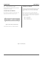
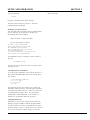
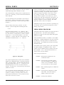
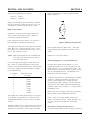
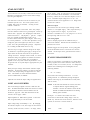
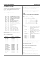
IDC connectors ar e pinned out as shown below. The
square pad, visible on the circuit side, is pin 1.
Phone: 303-690-1588
FAX: 303-690-1875
email: info@remotep. com
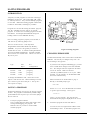
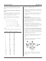
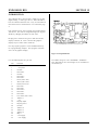
Figure 1-1 IDC connector viewed from top.
Ten and 20 pin connectors are similarly number ed.
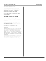
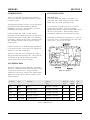
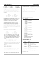
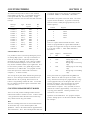
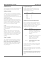
Figure 1-2 System layout
Page 1-2
SETUP AND OPERATION
SECTION 2
4.75 volts and below. The board may be operated
at up to 5. 5V witho ut damag e. C urre nt rating is
based on no loads at the digital ports and should be
increased based on requirements. If you are using
an opto rack, each module requires 15 mA. An
LCD display with LED back light on require s .5
amps. The 10-bit A-D converter normally uses
+ 5V as a reference. This is desirable if readings
are ratiometric or not critical. See Section 10,
ANALOG INPUT under "10 BIT A -D
CON VERT ER" for more inform ation.
INTRODUCTION
SETUP AND OPERATION
SECTION 2
The RPC -400 is ready to program as soon as you
connect it to a PC and apply power. This section
describes the steps needed to get a sign on message and
begin programm ing.
PC r equirements to load the compiler and set up your
operating environment are discussed. A "W here to go
from here" section tells you w hat sections to r efer to in
order to use the various capabilities of the RPC-400.
' + 15' should be + 9 to + 16 volts @ 50 to 150 mA.
If the system uses 4-20 mA current loop or 0-10V
D/A output, supply voltage must be a minimum of
+ 13V. C urrent output depends upon number of 420 mA or D /A outputs. R S-232 outputs at J8, J9,
and J11 use this same supply as does the A-D
converter circuitry.
OPERATING PRECAUTIONS
The RPC -400 is designed to handle a wide variety of
temperature ranges at low power. These characteristics
requir e using CM OS com ponents. CM OS is static
sensitive. T o avoid damaging these c omponents,
observe the following precautions before handling the
RPC-400.
1.
2.
' -15' supply is -8 to - 16 vo lts @ 50 mA . T his
supplies D/A outputs, A -D inputs, and RS-232
outputs.
Ground yourself before handling the RPC -400
or plugging in cables. Static electricity can
easily arc through cables and to the card.
Simply touching your PC before you touch the
card can greatly reduce the amount of static.
' CLP ' supplies the cur rent loop p ower . N orm ally it
is + 13 to + 36 volts @ 80 m A. This supply is
necessary only if you are using 4-20 mA current
loop output at P4. You can use + 15 power
provided transmission distances are short and load
resistance is 500 ohm s or less.
Do not insert or remove components when
power is applied.
EQUIPMENT
' PWR' at P5. T his is intended to supply either -21
volts for a graphics LCD display or additional + 5V
for a vacuum florescent. Refer to the display
section for more information.
A development system provides all of the parts necessary
to program and oper ate the card. You need to supply a
386 or fa ster PC with an RS -232 seria l port.
Power Supply
The dev elopmen t system includ es a powe r supply
capable of operating the board. There are some
limitations on this supply in certain situations.
4 - 20 mA Cur rent loop output requires a minimum of
+ 13 volts to operate using a 500 ohm terminator
resistor. T he development power supply will not output
enough voltage. A 250 ohm r esistor will work as the
terminating resistor.
Be careful when using some switching supplies. Some
switchers require minimum loads that may not be met
when connected to this card.
Supply rise time should be as quick as possible. The
penalty using a slow supply is garbage output of the RS232 ports. The C PU is n ot sending data as it is held in
reset. H owever, as the + and - 15 volt supplies rise, the
output changes and can give the appearance of sending
data.
If you wan t to use your own supply , m ake sure it meets
the following requir ements. Designatio ns in single
quotes are those marked at P1.
' 5V' + 5, ±0.25 V @ 0.5A . Reset voltage is about
Page 2-1
SETUP AND OPERATION
SECTION 2
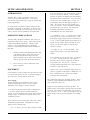
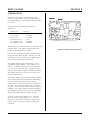
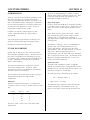
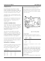
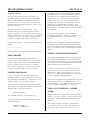
Figure 2-1 RPC-400 board power and programming ports.
Personal Computer (PC)
The PC used to compile and upload programs to the
RPC-400 must be a 386 or "better". There are no real
minimum speed r equirements. The penalty for using a
slow computer is increased compile and linking time.
One serial port is used to download, debug, and
communicate with the RPC-400. Comm unication speed
is set at 9600 baud.
The compiler, linker, and debugger use a DOS
environment. DOS should be 3.3 or higher.
You may write - compile - link - and upload programs
over a network. This has been successfully done using
Microsoft (tm) Windows (R) version 3.11 and Windows
95 operating system s.
You should have about 10 Meg of free hard disk space
available for saving pr ogram s.
PC SETUP-COMPILER INSTALLATION
The developm ent system consists of a set of disks.
These disks contain the compiler, libraries, source code,
and demonstration program s. These ar e saved to various
subdirectories in the computer. The root directory
defaults to ' RPC-GN U' unless you supply an additional
parameter in the DOS command line.
Loading the Disks
Make sure you ar e in the DOS root directory.
C:\
Insert disk 1 into the A: drive.
Page 2-2
SETUP AND OPERATION
Type the following:
SECTION 2
files as necessary.
a:install
Program is installed to RPC-GN U directory.
The files will now unzip to your drive. Insert the
remaining disks as prompted.
Modifying your Environment
The DOS path and environment must be modified before
you can run many of the progra ms. M odify your
AUT OEX EC. BAT file as follows:
Add to the path: C:\ RPC-G NU\ BIN
Set your enviro nment as follows:
SET PATH=c:\devl\gnu\BIN;%PATH%
SET GCC_EXEC_PREFIX=c:\devl\gnu\LIB\
SET INFOPATH=c:\devl\gnu\INFO
SET C_INCLUDE_PATH=c:\devl\gnu\include
SET CPLUS_INCLUDE_PATH =
c:\devl\gnu\include\cxx;c:\devl\gnu\include
SET GO32=EMU c:\devl\gnu\BIN\EMU387
Set TMPDIR to point to a ramdisk or other temporary
directory.
SET TMPDIR=c:\temp
You can also run the batch file SETENV.BAT and it will set
up things for you.
Verifying Software Installation
To ver ify prope r installation, set the curr ent directo ry to
\RPC -GNU\ RPC400\D EMO and execute the batch file.
For example:
c:>\RPC-GNU\RPC400\DEMO demo
gcc -O -x -G demo.c
ld -Trpc400.cmd
hint com1
This batch file invokes the compiler (gcc), linker (ld),
and HINT terminal program . These pr ograms should be
in the RPC-GNU\ BIN directory. If they are, then check
your DOS path by typing in SET. One of the paths
should point to \ RPC -GNU \BIN . Y ou will have to
modify your AUT OEX EC. BAT file to do this.
Changing Batch Files
Batch files are used to edit, com pile, link, and run the
debugger program (GDB) or term inal program (HIN T).
The files assume you will be using DOS EDIT to make
program changes. Ther e is a good chance you will want
to use your own editor, so make changes to the batch
Page 2-3
SETUP AND OPERATION
SECTION 2
If your se rial por t is not CO M2, type < Ctrl> -C to
exit the terminal program HINT. Then type HINT
COM 2.
OPERATING THE RPC-400
This part will power up the RPC -400, get a sign on
message, and run the demonstration program.
If you did not run the above program, make sure
you are in the \RPC-GNU\RPC400\DEMO
directory.
Become familiar with the locations of connectors before
getting started. See figure 2-1. Jum pers are set at the
factory to oper ate the system imm ediately. F or first
time installation, do not install any co nnector s or par ts
until specified below.
1.
At the DOS prom pt, type
HINT COM1
Connect power.
The RPC-400 needs + 5 and ±15 volts, as described
above unde r "P ower Supply" . T he developm ent kit
includes a power supply (which should not be
plugged in to the AC outlet at this time). C onnect
the wires from the power supply connector to the
board as follows:
PS connector
wire color
Red
Black
Orange
White
P1 designator
+ 5V
GND
+ 15
-15
If you are connected to COM2, enter that port
instead of COM1.
4.
Power up.
Turn on your pow er supply. On pow er up a message
is printed.
C Monitor. Hitachi Micro Systems, Inc. for the SH-1
Enhancements by Paragon Innovations, Inc, [CMON Rev..
Additional enhancements by Remote Processing, Corp.
$S05#b8CMON>
The "$S05#b8" text is for the GDB debugger after a
reset.
5.
Connect the cable from the power supply to the
power supply connector just attached to the board.
Don' t plug in the power supply to an A C outlet just
yet. If your power supply happens to have an extra
black wire, conne ct it to ground.
Testing.
The card is now ready to load a program. Hit enter
a few times to make sure the CMON> prompt comes
back. Type in the following command line to load
in the demo program:
l:demo.sr
2.
Hook up to a PC.
Conne ct the 10 pin side of the VT C-9F serial cab le
(P/N 1041) to J9 (also designated as COM 0).
Connect the other end to COM 1 or COM 2 on your
serial por t.
NOTE: Batch and com mand files assume C OM 1 is
the default port. If you cannot use CO M1, you must
modify all .GSC and .BAT files and change
references from COM 1 to COM 2.
3.
Run HINT.
If you ran the batch file under "Verify Software
Installation" above and did not exit out of HINT,
you might be ready. The batch program above
assumes the RPC-400 is connected to COM 1 on the
PC.
You will see progress of the program downloading to the
card. Download take s about 2 minutes.
When downloading is done, you w ill see the low, high,
and starting address. For example:
LOW
ADDRESS: 09002000
HIGH ADDRESS: 09005747
START ADDRESS: 090025F4
Type in the letter ' g' and the start address you see on the
screen. For example:
g 90025F4
The program will now execute. View the scr een for
further information. To stop execution, press the reset
button.
Page 2-4
SETUP AND OPERATION
SECTION 2
RUNNING DEMO PROGRAMS
All demonstration program s are in the ' RPC400'
directory. Each demo program uses either the GDB
debugger or HINT communication program. Programs
can be linked to use either debugging method.
All demo program directories have a batch file which
calls the DOS editor to make changes to the program,
compiles, links it and calls one of two programs to load
the progra m into the board. Some dem o progra ms use
the GDB debugger while others use the HINT program.
View the batch file to deter mine which one it uses.
Refer to Section 16, PRO GRAM MING NO TES,
LINKING PROGRAMS for information on changing the
linker command file for debugging.
A com mon load form at is used whe n HIN T is used to
load progra ms:
l:rpc400.sr
Enter this command after a boar d reset or at a command
prompt while running HINT. T he file 'rpc400. sr' is an
S record file. This file name is specified in the linker
command file.
It is a good idea to read the C source file before running
a demo program . The fir st part will tell you what the
program ' s purpose is and what to expect as an output. If
your car d does not have CO M2 and C OM3 serial ports,
you cannot run any of the programs that use them.
Page 2-5
SETUP AND OPERATION
SECTION 2
WHERE TO GO FROM HERE
If you want to do this:
Save a program
Run a program at power up or
reset (Autorun)
Know m ore abo ut serial por ts
Adding and using data RAM
Using digital p orts
Add a clock/calendar
Add battery backed RAM
Use display port
Connect a keypad
Meas ure voltag es (analog inpu t)
Enable the watchdog timer
Use exte rnal inter rupts
Connect a proximity sensor
Connect a quadrature encoder
Measure pulse periods
Use the vo ltage outputs
Use the 4- 20 mA outputs
Add other devices
How to start writing your own programs
Know more about the progr amming
environment
Turn to
Section
3
3
4
5
6
7
7
8
9
10
11
12
13
13
13
14
14
15
16
16
Page 2-6
SAVING PROGRAMS
SECTION 3
INTRODUCTION
S A VI N G P R OG R AM S
SECTION 3
Tempor ary or final program s are stored in a flash type
EPROM in socket U23. This socket holds 32K, 128K,
or 512K byte devices. They can hold multiple programs
or stor e data. Maxim um r unning pr ogram transfer rable
to RAM is about 240K, e xcluding any variables.
Programs are saved to flash using the monitor program.
The ' SF' command saves the start-up, or autorun
progr am. It can also save se condar y progr ams and data
from RA M. An example flash EPRO M saving and
loading routine is in the EPROM1 director y.
Once a w orking pr ogram is proper ly saved to flash, it
will auto run by removing jumper W 16.
The IC in sock et U23 is a 5-volt only Flash
Program mable and Erasable Read O nly Memor y
(PER OM ). A ny sector can typically be written to
10,000 times or m ore. A software locking mechanism
preven ts accidental m odifications. Prog ram s and data
can be written over 10,000 times. This is over twice a
day for 10 year s.
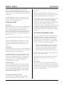
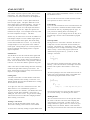
Figure 3-1 Saving Programs
CHANGING EPROM SIZE
The RP C-400 nor mally come s with a 32K or 512K flash
EPROM . The size may be changed at any time. Set
W7 according to the type/size.
Type
29C256
29C010
29C040
Size
Bytes
32K
128K
512K
If you have b een using the G DB debug ger, you will
have to make minor changes to the link command
file. The changes make the output from the linker
into an 'S' format. Make sure the line
(OUTPUT_FORMAT fname. sr) is in your .CMD
link file. For an example, see the RPC400.CMD
file in the AIN3 directory.
W7
Configuration
[3-5],[4-6]
[3-5],[2-4]
[1-3],[2-4]
To change the EPRO M in U23, remove the IC and
replace it with the new one. Whe n installing a 29C256,
pin 1 on the IC goes into socket pin 3. The top two
rows of pins are empty.
HINT instructions are in SECTION 2, page 3.
Briefly, at the DOS prompt type:
HINT COMn
SAVING A PROGRAM
Where n is 1 or 2. Pr ess the RPC-400 reset button
to get the sign on message. Then type in:
Perform the following steps to save the start up program
to flash. This program is automatically loaded to high
speed RAM and run on power up or reset when jumper
W16 is removed.
1.
Load your program to RAM.
You' ve alrea dy done this m any times b efore w hile
writing and debugging your program . The
difference here is you have to use the HINT
terminal program.
l:fname.sr
fname. sr is your pr ogram . T he prog ram will
download and the progress displayed on the screen.
2.
Determ ine progra m size and start addr ess.
You will see the low, high and start address when
downloading is done. To determine program size,
Page 3-1
SAVING PROGRAMS
subtract the high from the low address. You may
need to use the hex calculator in the monitor.
To use the monitor's hex calculator, use the 'P'
comm and to print the value. For exa mple, suppose
the high addr ess is 900E7 F8. Low a ddress is
9002000. Enter:
SECTION 3
Problems
The C OM 0 port is not initialize d when au torun is
enabled. CO M0 will work if the board w as powered up
in the monitor mode first. M ake sure you initialize
COM 0.
CMON> p 900e6e8 - 9002000
The result is pr inted back as:
decimal 50920
CMON>
hex 0000C6E8
Program length is 50920 bytes. Length is entered as
a hex number and rounded up to C 800.
Entered param eters are always in hex. Star ting
address is always 9002000, if you keep to the
defaults. When you have determ ined the size, round
it up to the next even page size. Example: P rogram
size (in hex) is 6247, r ound it to 6400. T his is,
effectively, the nu mber of b ytes flash will use
anyway becau se of progra mming r equireme nts.
Starting address is displayed on the screen.
3.
Save it to flash
The SF comm and saves pr ogram s to flash. Type in
the following command:
CMON> SF 9002000 length start_address
Prog ress is display ed on the scr een while
program ming. P rogram ming time depends upon the
length and flash EPROM type. A 512K type
program s 512 bytes in about 10 ms.
Testing is as simple as removing jumper W16 and
resetting the board. Your program should run.
AUTORUN
The RPC -400 is set to autorun on power up or reset by
removing jumper W16. At power up or reset, the BIOS
reads this jumper. If it is open, it loads the program
previously saved in U23 to RAM. It then jumps to the
start address, defined at address 0x9002000. Program
execution begins from there.
Page 3-2
SAVING PROGRAMS
SECTION 3
FLASH DEMO PROGRAM
A flash EPRO M demonstr ation program is in the
EPR OM 1 subdire ctory. This pr ogram uses HIN T to
download and run th e progr am. C F ile name is
EPROM1 and run time file is RPC400.SR.
Use the sample program for routines to save data or
program s to flash.
MEMORY MAP - FLASH EPROM
The F lash EP ROM is in CPU mem ory ar ea 2. It is
accessed 8 bits at a time, so its addres s is 0x2000000 to
0 x2 07 F FF F .
RAM in U24 is also in CPU mem ory ar ea 2. It is
accessed starting at 0x2080000. See SECT ION 5 for
more information on RAM.
See Table 5-1 for a complete mem ory map.
Access time
Flash E PRO Ms hav e access tim es of 100 nS. The w ait
state controller WCR1 should be set so area 2 has one
long wait plus th e numbe r of wa it states specified in
WCR 3. Refer to the SH-1 Hardwar e manual, Section 8,
Bus State Controller, for more information. The BIOS
leaves the r egister setting s alone as the po wer u p defaults
are adequate.
If you are going to r un progra ms directly fr om the flash
EPR OM or RA M, then you can shorten up the time to
reflect the access time of the device you are using.
Page 3-3
SERIAL PORTS
SECTION 4
Initialization
The CM ON BIOS initializes COM0 on pow er up or
reset and auto-run is not selected. It is a good idea to
initialize COM 0 in your prog ram if you intend to use
this port during run time. T he problem is when you
auto-run your program after a power up, COM 0 won' t
get initialized. Initialized settings are not changed on a
push button r eset.
INTRODUCTION
SERIAL PORTS
SECTION 4
The RP C-400 is available with either 2 or 4 serial por ts.
The 2 port version has RS-232 I/O. The 4 serial port
version has three RS-232 I/O. The fourth is isolated and
jumper selected for RS-232 or RS-422/ 485.
COM0 is normally used as a debugging port. However,
during run time it may be used as any other serial port
provided you do not use the GD B debugger. You must
use HINT or the device you intend to connect to COM 0.
You may use the GD B debugger if you don' t care about
any output from COM 0.
All of the demonstration programs use either C OM0 or
COM 1. Initialization routines for COM1 ar e in the
400IO sub-directory and file. The 400IO.C file also has
general purpose get and put character and string
routines.
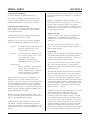
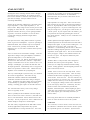
Figure 4-1 Serial Ports
RTS and CTS Lines
CTS and RT S lines are u sed for ha rdwa re flow control.
The SH-1 processor does not have these lines as part of
its UART. They are brought out digital ports on the
CPU where its function may be emulated.
Schematics are on pages 6 and 7.
COM0 AND COM1
Description
Both of these ser ial ports func tion identically. COM 0 is
used as the pr ogram ming por t. D uring r un time, this
port may be used like COM 1. C OM0 is initialized by
the BIOS only when the auto run jumper is installed.
For cold power up, C OM0 m ust be initialized, if used.
Names for C TS and RTS lines is a source of confusion.
Normally, CTS is an output from a PC. On the RPC400, C TS is an input on COM0 and an output on CO M1COM 3. Conversely, CTS is a PC input while it is an
output on COM 0. T he discussion that follows will use
the PC convention. Keep in m ind that the names and
functions are reversed on CO M0 only.
Detailed programming information is in the SuperH
RISC Engine Hardware Manual , section 13.
R TS is us ed by a rec e ive r to indic a te if "O K t o send". A
high level at the connector indicates yes, ' send data'
while a low level indicates ' hold off' . T his line goes to
a sender CTS pin to signal conditions stated above.
COM 0 and COM1 are pr ogrammable for baud rates
between 110 and 38400. (W hen you refer to the baud
rate tables, the cpu clock is 19.6608 Mhz.) Other
programming capability include data length at 7 or 8
bits, 1 or 2 stop bits, and none, even or odd parity.
The CTS input line on COM1 and RTS input on COM0
have a 4. 7K ohm p ull up to + 5V at the co nnector . T his
is to enable communication if this line was missing on
the external device.
COM 0, a t J9, is a 1 0 pin IDC connector . Its pin o ut is
at the end of this sec tion. U se the VT C-9F serial cab le
to connect fr om C OM 0 directly to a PC. Table 4-1 is
the connecto r pin out.
CTS works nicely as a hardware hold-off. It can
generate an interrupt when it goes high and there are
charac ters to tra nsmit. Howe ver, when C TS chec king is
operated in polled mode, the line must be checked every
time a character is transmitted. Should the receiver
signal "h old off" , the progr am m ust wait fur ther until
CTS goes back high.
COM 1, at J11, is a 9 pin male D-SUB. Pin out matches
that of a PC. Table 4-2 is its connector pin out. Notice
that not all pins are used.
Page 4-1
SERIAL PORTS
SECTION 4
major difference is CO MM 23.C operates the RS-485
serial por t.
Ther e are sev eral com plicated schem es wher e this
software CT S/RTS line monitoring problem can be
solved, but they are complicated. The next best solution
is to have the r eceiver send an XO FF /XO N char acter to
control flow.
Buffer sizes were arbitrarily chosen at 256 bytes. It
could be increased to any size. The buffers are circular.
Read the notes in the files for more explanation.
CTS/ RTS lines must be read or set by software. The
program COM M1. C in directory CO MM 1 shows how
these lines are read and manipulated.
There is plenty of processing power to operate all serial
ports (COM0 - CO M3) in interrupt driven mode at
maximum baud r ate. Using the sample C OMM 22.C
program as a bench mark, interrupt service time is about
12 micro-sec onds. A ssuming a char acter is also
received, 24 X 4 ports + overhead . 100 micro-seconds
per character. At the maximum baud r ate of 57600 (not
available on COM0 and C OM1), there is still over 70
micro-seconds available for other processing, including
interrupts.
COM2 AND COM3
Description
COM 2 and COM3 use a 8250 software compatible serial
interface chip. This is the sam e type of U ART used in
PC' s. Capa bilities include CTS and RT S control
signals, program mable character lengths (5-8), and even,
odd, or no par ity. Baud rates are progr ammable from
50 to 115.2K. Each port may gener ate an interrupt on a
transmit or receive.
ISOLATED COM3 SERIAL PORT
The CO M3 serial port is an optically isolated RS-232 or
RS-422/485 serial port. Isolation is adequate for low
voltage (less than 100 V) cir cuits, when the b oard is
operated in an environment relatively free of moisture
and dust (Reference UL 1950, Table 3, Pollution degree
1 and 2). Transients should be less than 750 V.
Prog ram ming infor mation ab out this chip is in Ap pendix
A.
COM 3 is optically isolated w hile CO M2 is not. Both
ports hav e PC compatib le DB-9 m ale connec tors. Pin
out for thes e connector s are listed at the end of this
section.
NOTE: The RPC-400 board was NOT tested to UL
1950 or a ny other sta ndards. We do no t imply it
will mee t this or any oth er standa rd. Isolation is
provided to remove small AC ground and DC
offsets normally found in long distance connections.
Initialization
The CM ON bios does not check to see if the COM2 and
COM 3 serial chip (U43) is installed. This chip must be
initialized as must the CPU interrupt por ts.
Both ports sha re the sam e UA RT. Conseq uently, only
one port can be used at a time.
Initialization routines and basic drivers (putchx, putsx,
getchx) are in 400IO .C , in the 400IO directory. These
routines are for polled mode only. For interrupt driven
serial routines, look in the COM M02, COM M22 and
COM M23 d irector ies. L ogic for C OM 3 RTS is
reversed. Read next paragraph.
RS-422/ 485 are from screw termin als at P6. RS-232 is
from a DB-9 m ale. See Figur e 4-1 for connector
location.
LED Activity
There are tw o LED ' s on the RPC-400 which blink on
when there is transmit or receive activity. D1 is amber
and blinks when receiving. D2 is green color and blinks
when transmitting. Brightness is dim when sending few
characters at a high baud rate.
COM 3 RTS Logic
Logic for COM3 RTS output is reversed from COM2
and nor mal P C oper ation. This wa s done beca use this
line controls the RS-485 transmitter. The logic is such
that on power up, the 485 transm itter is off. The RS232 RTS output line on COM3 w ill be high, signaling
OK to transmit to another device.
I n te r rupt Dr iv e n C O M 2 an d C OM3
Two sample r outines, COM M22. C and CO MM 23.C
operate COM 2 and COM 3 in interrupt mode. T he
Page 4-2
SERIAL PORTS
SECTION 4
The RS-232 transmitter is always enabled. Use this port
to monitor transmit activity on RS-485 to a terminal or
another PC.
Configuring Isolated RS-232
Set jumper W12[2-3] to enable RS-232 receive.
The CT S line at COM3 is pulled high through a 4.7K
resistor to enable communication. This is provided
should the external device be missing the CTS line.
RS-422 is a long distance version of RS-232. The
transmitter a nd receiver s are always on. To use P6 as a
RS-422, simply set RTS3 line high. See program
comm23. c for code and comm ents. Set jumper W 11[12] and W12[1-2]. The terminator at W13 should be set
to reduce ringing and noise.
Configuring Isolated RS-422/485
There are thr ee sets of jumpers affecting RS-422/485.
Refer to F igure 4-1 for the loca tion of these jumpers.
Each is described below.
Wiring for RS-485
Four wire systems simply connect corresponding TX±
and RX± lines. Unfortunately not all systems are
mar ked the sam e so you m ay have to pla y aroun d with
signal wires.
Set jumper W12[1-2] for all 422/485 com munication.
This jum per selec ts the rece ive signal.
Jumper W 11 is set in one of two positions, depending
upon the communication standard and mode desired.
W11[1-2]
4 wire RS-485 mode (separ ate TX and
RX lines) o r RS-42 2 mode. This
always enables the receiver.
W11[2-3]
2 wire RS-485 mode. Externally wire
TX+ to RX+ and TX - to RX-. This
turns off the receiver when
transm itting. T he RTS 3 line is
manipulated to do this. (More later)
The ' GND ' line at the 485 con nector is fo r the cable
shield. This line goes through a 100 ohm resistor to an
internal, floating ground.
Using RS-485
RS-485 is use d in a multi-dr op (netwo rked) en vironm ent.
The auth ors of this stan dard do not specify a pr otocol.
RS-485 is only a hardware specification. 32 units over a
4,000 foot range can be connected together.
There are sever al questions users have when using RS485. Two of the most pop ular ar e: W hat baud r ate
should I use (or what is the m aximum ) and the seco nd is
about the pr otocol.
W13[1-2][3-4]
Network terminators. Set only when
the RPC -400 is physically the last
board in a RS-485 system. Otherwise,
remove these jumper s. In RS-422
systems, keep these jumpers in.
The maximum baud rate depends upon the environment
all of the boards will operate in. If you are installing a
network, or can specify cable type, make sure it is one
for RS-485. This cable has low capacitance, twisted
signal wir es inside a shield. Belden type 984 2 or 9844 is
a good starting point for cables. Critical characteristics
are twisted pair with shield, . 100 ohm impedance cable,
and low capacitance. Capacitance is not critical when
distance is short (< 1000 ft).
The RTS3 line acts the same way as in RS-232. The
difference here is it controls both the receiver and
transmitter. In two w ire mode, it prevents the data sent
out from looping back and getting received. RTS3 line
is set in the UART MC R to ' 0' to enable transmitting
and disable receiving and '1' to disable transmitting and
enable receiving. See demo program COMM23.C for a
sample of RS-485 in 2 wire mode.
Ultimately, the only way to determine this is to view the
RS-485 signal using an oscilloscope. Set up the
"near est" tr ansmitter to continuously se nd a signal.
Look at the result on the "farthest" receiver. A rough
rule of thumb is maximum baud rate should be 6 times
or m ore of the worse of rise or fall times. The idea is to
present a clean, steady signal to the receiver. Rise and
fall time should be less than 30% of the total bit width.
Measurement should be taken at the farthest receiver
with all device s connected . T he farthe st receive r should
have its terminator installed. No progr ams have to be
RS-485 is be st when ope rated in inter rupt m ode. This
way, the transm itter is shut off w hen the last cha racter is
sent out. See COMM 23.C for exam ple.
In practice, there is little difference between 2- and 4wire RS-485. Hardwar e simultaneously controls the
receiver and transmitter. The only real difference is the
board cannot receive data while transmitting in a 2-wire
system.
Page 4-3
SERIAL PORTS
SECTION 4
A slow, but reliable peer to pee r networ k is to use
round-r obin com municatio n. Su ppose on pow er up unit
1 sends out a m essage. All the other units recog nize to
whom the message is intended. If the receiver is off
line, nothing is returned. Unit 1 can' t send another
message until it is spoken to or its turn is up. After a
period of time, unit 2 has perm ission to use the line. In
a similar manner as unit 1, it sends out a message and
waits for a respon se. If unit 2 is off line, unit 3 will
speak after unit 2' s time out is complete.
running. Our cu stomer s experie nce is has bee n 4800 to
19200 baud using 3000 to 5000 feet of cable.
The second question is about protocol. RS-485 does not
specify one. Gener ally, you can treat the data format the
same as RS-232.
A 4-wire multidrop networ k includes a host and one or
more de vices. T his is a master-slave system . the host
directs all comm unication. N odes "do not speak unless
s po k en to . "
Additional messages can be generated to speed things up.
For exam ple, one is to tell the next unit in line "I have
nothing, you go ahead. "
Ther e are m any mas ter-slave p rotocols. For this
example, a protocol might look som ething like this:
>22M1B1
SERIAL DEMO PROGRAMS
The pr otocol starts w ith the < cr> charac ter. This
character synchronizes all units and alerts them that the
next few characters coming down are address and data.
In this case, "> 22" is the units address. "M " is the
command, "1" is data, and "B1" is the checksum. The
command is terminated with a < cr> character.
COM 0 and COM 1 demo program s are peppered in all of
the sub-directories. All of the counter programs
(PWM x) use COM 1 for main output while analog input
(AINx) use CO M0.
COM 1 initialization routine is in 400IO.C, in the 400IO
subdirectory. C OM0 initialization is the same except for
the addresses. Interr upt routines are contained in the
entire pr ogram . T his includes the inte rrup t vector tab le
and enable routines.
Print routines such as getchx, putchx, putsx, and printfx
are either in 400IO .C or PRIN TFx. C files. These
routines are in the 400IO.A library, called by all of the
other programs. T he ' x' after the function name (i.e.
putchx) refers to the port number.
Other serial port routines are:
Figure 4-2 Data packet
The response depends upon the nature of the command.
Suppose the command M means "r eturn the belt speed"
and 1 is the belt number. The R PC-400 could read the
port and respond with A2.34< cr> . The first A is an
acknowledge, that is no error s were detected in the
message. The data, 2.34, can mean feet per unit of time
(minute or second).
A 2-wir e networ k can have m ultiple hosts. This " peer to
peer" networ k can be a bit more complicated. T he
problem is avoiding or resolving conflicts when two
peers speak at the same time. 2-w ire protocols can be
master-slave, the same as 4-wire.
Page 4-4
COM M01
Read/control C TS/RT S lines for
C O M 0 a nd C OM 1
COM M02
Interrupt driven terminal program,
with error handling, for COM 0 and
COM1. Drivers in 400IO.C library
are not used but are in this program.
COM M21
Basic terminal program for COM 2 and
COM 3.
COM M22
Interrupt driven example for COM2
and CO M3. Note that r outines in
400IO.C library are not used.
COM M23
Interrupt driven RS-485.
SERIAL PORTS
SECTION 4
SERIAL CONNECTOR PIN OUTS
Table 4-1
COM 0 connector pin out is as follows:
Pin
Name
Direction
from card.
3
4
5
6
9
10
Tx
RTS
RXD
CTS
Ground
+ 5V
Out
In
In
Out
A VT C-9F serial cab le for C OM 0 is made b y simply
taking a 10 pin female IDC connector and crimping a 9
wire r ibbon cable to it. The, crimp a 9 position fem ale
D-SUB connector to the other end of the cable. W iring
is one to one.
Table 4-2
COM1 - COM3 RS-232 pin out is as follows
D-SUB Name
Pin
Direction
from card.
2
3
5
7
8
In
Out
Rx
TX
Ground
RTS
CTS
Out
In
Pin out from the 9 pin male D-SU Bs matches those on a
PC. Use a null modem adapter w hen connecting
between a PC and C OM1 - 3.
COM2,3 ADDRESS AND INTERRUPTS
Port
Base
Address
C O M 2 0x6000080
C O M 3 0x6000100
IRQ
1
2
See Appendix A for detailed U43 UA RT progr amming
information. IRQ 1 and 2 ar e CPU interrupts.
Page 4-5
MEMORY
SECTION 5
INSTALLING RAM
INTRODUCTION
MEMO RY
SECTION 5
There a re severa l different mem ory types and ar eas.
Their types, functions, and address locations are shown
in Table 5-1 below.
Data RAM U24
Socket U24 holds 32K, 128K or 512K RAM . Set
jumper W8 to the ' 128K' position for 32K or 128K
RAMs and to the ' 512K' position for 512K.
The application pro gram is stor ed in a 5-volt only Flash
Program mable and Erasable Read O nly Memor y
(PEROM ) in socket U23. See SECTION 3, SAVING
PROGRAMS for saving information.
To install RAM, orient the chip so pin 1 is near the
outside edge of the board. If you are installing a
calendar /clock module o r batter y backup m odule, install
this into socket U24 first. W hen installing 128K or
512K RA Ms, simply inser t the RAM into the socket.
Socket U24 holds 32K, 128K, or 512K of RAM.
Optionally, a clock/calendar w ith battery backup may be
installed in this socket (see SECTION 7 for installation
inform ation). Mem ory in this soc ket is intended to ho ld
data, although pr ogram s could run from it at greatly
reduced speed.
32K RAM s are installed by leaving pins 1,2, 31, and 32
open in the soc ket. Orient the RAM so pin 14 goes into
socket pin 16. The top rows ar e open.
Sockets U25 and U26 use 128K byte high speed RAMs
for program execution. These sockets are organized as
128K X 16, for a total of 256K bytes.
Sockets U25 and U26 can be configured for 512K X 8
high speed RAMs through jumper W6. This option was
not available at the time this manual was printed.
Contact Remote Processing for an update.
ACCESSING RAM
Review the sample program in 'EPROM1' and RAM1
directories. EPRO M1 tra nsfers data from RAM to flash
a character by character basis. Integers and other
numbers are read from or written to in a similar manner.
RAM 1 stores all da ta types to RA M. View the results
using the monitor.
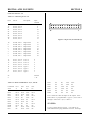
Figure 5-1 Memory
Location
Type
Function
Address
range
Memory
Area
Access
Width
Max
size
U22
ROM
BIOS
000 0000 - 000 FFFF
0
8
64K
U23
Flash
Program storage
200 0000 - 207 FFFF
2
8
512K
U24
RAM
Data and clock
208 0000 - 20F FFFF
2
8
512K
U25, U26
Fast RAM
Program execution
900 0000 - 90F FFFF
1
16
1M
U21
CPU RAM
Genera l purpose
FFF E000 - FFF FFFF
7
32
8K
Table 5-1 Memory M ap
Page 5-1
MEMORY
SECTION 5
Program execution U25, U26
High spee d 512K RA Ms in D IP for m we re not r eadily
available at the time of this printing. Remote P rocessing
may make an adapter board so higher density RAMs
may be installed. This section deals with changing the
jumpers.
BIOS EPROM
Jumper block W6 sets the BIOS and program execution
RAM size. To use 128K RA Ms, set jumper W8[3-4].
For 512K RA Ms, set W8[4-6].
If you modify the BIOS and program size exceeds 32K,
you will need to use a 27C512 EPROM . Jumper W6[12] must be set to access this 64K device.
The BIOS resides in socket U22. The BIOS is accessed
on power up and during program development. As
shipped, it is a 32K byte device. Norm ally, you will not
have to wo rry a bout it.
RAM installation will be a m atter of r emoving the old
parts and installing the new ones.
Page 5-2
DIGITAL AND I/O PORTS
SECTION 6
INTRODUCTION
DIGITAL AND I/O PORTS
SECTION 6
Digital I/ O lines ar e used to inter face with op to-module
racks, switches, low current LED's, and other TTL
devices . T hese line s are b roug ht out via S TB-26, STB20, or MP S-XX opto r acks.
Digital lines are available fr om multiple sour ces.
Connector J6 is considered the primary source.
Additional lines usable as digital I/O are available from
the keypad (J2), display (J4), and CP U (J1 analog input
and J13 GPIO) for a total of 69 digital input and output
lines. Some of these lines are intended for other
functions and its use must be considered in the system
design.
General warnings and precautions
WARNING:
Apply power to the RPC -400 before applying a
voltage to the digital I/O lines to prevent current
from flowing in and powering the board, damaging
devices. If you cannot apply power to the RPC -400
first, contact technical support for suggestions
appropriate to your application.
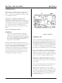
Figure 6-1 Digital I/O
J6 DIGITAL I/O
This por t is considere d the main digital I/O port. It is
used to interface opto modules (using MPS series racks),
drive small relays, solenoids, motors, or lamps, and
provide gener al purpose TT L I/O to other logic devices,
or mechanical switches. J6 is shown on schema tic page
5. Its address is 0x6000000 through 0x6000006. See
the program in the DIO directory for an access example.
When lines are configured for outputs at any of the
82C55 ports (J2, 4, and 6), outputs go low until set high.
Low lines turn on opto modules and potentially other
devices. One solution is to set the output lines
immediately after configuring them. Depending upon
how you have written your progr am, lines can be low
for less than a micro-second. T his low time can be
enough to cause problems with some devices. Power
opto modules are generally not affected.
Lines on J6 are divided into 3 eight bit groups from an
82C55. Refer to table 6-2 for a list of configuration
comm ands to wr ite to the 82C 55. A byte is wr itten to
address 6 (0x6000006). These command bytes configure
ports A, B, and C for inputs and outputs as shown.
When a line is configured as an output, it can sink a
maximum of 2. 5 mA at 0. 4V and can source over 2. 5
mA. Outputs sink over 15 mA at 1.0v, enough to drive
opto modules.
Port B is connected to a high current sink through U49.
See "High C urrent Output" later in this section.
Digital I/O lines are pulled to + 5 volts or ground
through 10K or 100K resistor packs using jumper W 10.
82C55 port A is p ulled up or down thr ough 10K. Ports
B and C through 100K. Upon reset or configuration as
an input, the lines will then be pulled high or low as
your system r equires.
Page 6-1
DIGITAL AND I/O PORTS
SECTION 6
Protection diodes m ust be used with inductive loads.
Refer to Figure 6-2.
Jumper W 10 configuration is as follows:
W10[1-2]
W10[2-3]
Pull up
Pull down
Setting W10 for pull up makes interfacing to switches
and "open collector" collector TTL devices easy. See
"Interfacing to Switches and other devices" below.
High Current Output
Eight lines at J6 can be used as high cur rent driver s.
These outputs switch loads to ground. Outputs are
controlled by Port B on the 82C55.
Logic outputs are inverted. W hen a 1 is written to a
line, the output is switched ON and goes low.
Figure 6-2 Inductive load protection
The output driver chip U49 can be replaced w ith a DIP
shunt jumper so it is like the other lines at J3. To do
this, r emove U49. Install a DIP shunt so pin 1 goe s to
pin 18. Pins 9 and 10 are open.
Do not pa rallel outputs f or higher drive. This could
result in damage since outputs will not share current
equally.
Outputs at U12 are open collector.
NOTE: High cur rent outpu ts are not co mpatible w ith
TTL logic levels and sh ould not be used to
drive other logic dev ices.
Interfacing Digital I/O to an opto-module rack
Each of the high current outputs can sink 500 mA at
50V. Howe ver, package diss ipation is excee d if all
outputs are used at the maximum rating. The following
conserv ative guidelines a ssume the number of outputs
are on simultaneously:
# of outputs
on
1
2
3
4
5
6
7
8
I/O lines can be interfaced to an MPS-8, 16, or 24
position opto m odule rac k. L ines not going to an opto
module c onnect to a scr ew ter minal on the racks. This
feature allows you to connect switches or other TTL type
devices to the digital I/O lines. The MP S-XX series
boards accept G 4 series modu les.
Maximum current
per output
A CM A-26-24 connects J6 on the RPC-400 to the MP SXX bo ard. Cable len gth should be less than 2 feet.
Excessive cable lengths cause a voltage drop and
consequently unreliable operation. This is because the
28 gauge wire in the ribbon cable has sufficiently high
resistance . M ake sure you connec t + 5 V and gr ound to
the MP S-XX r acks.
500 ma
400 ma
275 ma
200 ma
160 ma
135 ma
120 ma
100 ma
Before a line is set, the 82C55 chip must be initialized.
Refer to T able 6-2 for initialization param eters.
The ther mal time constant of the p ackage is ve ry shor t,
so the number of outputs that are on at any one time
should include those that over lap even for a few m illiseconds.
Refer to Table 6-1 for Opto module position, port
number, and connector pin out. If opto channels 16-23
are used, U 49 should be replaced by a DIP shunt
jumper.
Incandesc ent lamps h ave a " cold" c urre nt of 11 times its
operating current. Lamps requiring more than 50 mA
should not be used unless a series resistor is installed.
Interfacing to switches and other devices
Switches and other digital I/O devices may be connected
Page 6-2
DIGITAL AND I/O PORTS
SECTION 6
directly to J6. The STB-26 ter minal board p rovides a
convenient way of interfacing switches or other digital
I/O devices. Lines at J6 are connected to the STB-26
with a CMA-26 cable. Digital devices are then
connected to the screw terminals on the STB-26. Refer
to Table 6-1 for J6 connector pin out description. The
MP S-XX ser ies opto racks also prov ide a way to access
digital I/O lines.
Switches may be connected directly to a line. When
jumper W10 configures the resistors as pull ups, a switch
closure to ground at a line is read as a 0. When running
long leads (greater than 5 feet) or in noisy environ ments,
connect a 1K ohm resistor between + 5V and the switch.
When W 10 configures the input r esistors as pull downs,
one end of the switch m ust be tied to + 5 volts. If this is
not possible or convenient, a 10K resistor can be tied
between an input and + 5 volts to force it high when a
switch is open.
Page 6-3
DIGITAL AND I/O PORTS
SECTION 6
Conne ctor Pin O ut - J6
Table 6-1 Conne ctor pin ou t - J6
Pin #
82C55
Description
19
21
23
25
24
22
20
18
Port
Port
Port
Port
Port
Port
Port
Port
A,
A,
A,
A,
A,
A,
A,
A,
line
line
line
line
line
line
line
line
0
1
2
3
4
5
6
7
10
8
4
6
1
3
5
7
Port
Port
Port
Port
Port
Port
Port
Port
B,
B,
B,
B,
B,
B,
B,
B,
line
line
line
line
line
line
line
line
0
1
2
3
4
5
6
7
High
High
High
High
High
High
High
High
13
16
15
17
14
11
12
9
Port
Port
Port
Port
Port
Port
Port
Port
C,
C,
C,
C,
C,
C,
C,
C,
line
line
line
line
line
line
line
line
0
1
2
3
4
5
6
7
Lower C
Lower C
Lower C
Lower C
Upper C
Upper C
Upper C
Upper C
Opto
Channel
8
9
10
11
12
13
14
15
current
current
current
current
current
current
current
current
Figure 6-3 J6 pin out (viewed from top)
16
17
18
19
20
21
22
23
0
1
2
3
4
5
6
7
26
2
Ground
+ 5V
0x92
0x93
0x98
0x99
0x9A
0x9B
Table 6-2 82C55 C omm ands for J2, 4, and J6
Comm and
value
Port
A
Port
B
Port
UC
Port
LC
0x80
0x81
0x82
0x83
0x88
0x89
0x8A
0x8B
0x90
0x91
OUT
OUT
OUT
OUT
OUT
OUT
OUT
OUT
IN
IN
OUT
OUT
IN
IN
OUT
OUT
IN
IN
OUT
OUT
OUT
OUT
OUT
OUT
IN
IN
IN
IN
OUT
OUT
OUT
IN
OUT
IN
OUT
IN
OUT
IN
OUT
IN
IN
IN
IN
IN
IN
IN
IN
IN
OUT
OUT
IN
IN
OUT
OUT
IN
IN
IN
IN
OUT
IN
OUT
IN
OUT
IN
Port A and B are either all inputs or all outputs. Each
half of Port C is program mable. Upper C (UC) is bits 4
through 7 and Lower C (LC ) is bits 0-7.
J13 GPIO
J13 is a general purpose I/O port. It is made up of
multi-function lines progr amma ble as timers, interrupts,
Page 6-4
DIGITAL AND I/O PORTS
SECTION 6
J2, J4 OPERATOR INTERFACE
and bit programmable I/O. Refer to schematic page 3
for a wir ing diagram o f this port. T able 12-1 is a
connector pin out and general alternate function.
Ports J2 and J4 are intended to interface to a keypad and
display, respectively. If you are not using one or the
other, then they are available as digital I/O in a manner
very similar to J6, discussed above.
Your system requir ements determine the function of the
lines. This section discusses using some or all lines for
simple I/O functions. Refer to the interrupt and counter
sections of this manual for other uses.
These ports interface to an 82C55. Consequently,
programming and electrical characteristics are the same
as for J6. The exception is neither J2 or J4 has a high
current output. U se Table 6-2 above to configure the
82C55 por ts.
Po rt B I/ O
Primary C PU registers affecting port B functions are:
PFC_PBIOR, PF C_PBCR1, PFC _PBCR2, and PBDR.
PFC _PBIOR determ ines which lines are inputs and
outputs. PF C_PBCR 1 and PFC _PBCR2 determ ine the
function of a line such as interrupt, timing pattern, I/O,
or other as described in the hardware manual. See
SH7032 har dware m anual sections "Pin Function
Controller" and "Para llel I/O Ports" for more
information.
This port is accessed from 0x6000180 to 0x6000186.
The schematic for J2 and J4 is on page 4.
If you use only a few of the lines on either port as
inputs, be sure to tie any unused inputs to ground or
+ 5V. F ailure to do so could cause the board to draw
excess current and may damage the 82C55 device.
Unused ports may be configured for output in the
initialization section of your code.
On power up, the BIO S program s port B as follows:
PB0 - PB7 are outpu ts
PB8 - PB11 is serial communications
PB12 - P B15 are inp uts
Table 6-3 and 6-4 show the pin outs for J2 and J4. The
STB-20 brings out lines from J4 to a terminal strip for
easy access.
Thr ee re gister s are u sed to co nfigur e and ac cess por t B.
Section 15.3.3 in the Hitachi SH7032 Hardware Manual
describes PBIOR, which, in general, determ ines what
lines are inputs and outputs. PBCR1 and PBCR 2,
described in section 15.3.4, select the functions of the
pins. Section 16.3. 2 describes PBDR, which is the
actual data I/O register. A write to this register
determines the output level while a read returns the
curren t status.
Table 6-3 Conne ctor pin ou t - J2
Port B can also be used for counting/ timing functions.
Refer to Section 13, COUNTING/TIMING for more
information on alter nate uses.
See the DIO directory for port access example.
Pins are capable of driving standard TTL loads. The
table below shows the cu rren t output at a level.
Item
Output low level per p in
Output low level total
Output high le vel per pin
Output high level total
Pin #
Function
1
2
3
4
5
6
7
8
9
10
ROW 1, 82 C55 por t C, bit 0
COL 3, 82 C55 por t C, bit 6
COL 2, 82 C55 por t C, bit 5
ROW 2, 82 C55 por t C, bit 1
ROW 3, 82 C55 por t C, bit 2
COL 1, 82 C55 por t C, bit 4
COL 4, 82 C55 por t C, bit 7
ROW 4, 82 C55 por t C, bit 3
COL 5, 82 C55 por t B, bit 0
COL 6, 82 C55 por t B, bit 1
Note that tw o lines from 82C55 p ort B go to this
connector.
Current (ma)
There is a 10K pull up res is tor to + 5V on R OW1
through ROW 4 only. All other lines are open.
10
80
2.5
25
Table 6-4 Conne ctor pin ou t - J4
These levels apply only to J13. Input currents are 1 ua.
Do not exceed + 5V positive or go lower than 0V.
Pin #
Page 6-5
Function
DIGITAL AND I/O PORTS
1
2
3
4
5
6
7
8
9
10
11
12
13
14
15
16
17
18
19
20
SECTION 6
+ 5V supply
Ground
82C55 port A, bit 4
LCD contrast bias
82C55 port A, bit 6
82C55 port A, bit 5
82C55 port B, bit 7
82C55 port B, bit 3
82C55 port B, bit 2
82C55 port A, bit 7
82C55 port A, bit 1
82C55 port A, bit 0
82C55 port A, bit 3
82C55 port A, bit 2
82C55 port B, bit 4
82C55 port B, bit 6
82C55 port B, bit 5
To P5 , ' ADJ' pin
To P5 , ' PW R' pin
Ground
There are no pull up resistors on J4. All lines are open.
Page 6-6
DIGITAL AND I/O PORTS
SECTION 6
J1 ANALOG INPUT AS DIGITAL IN
J1 is a 10 bit, 8 channel A-D converter. The converter
is an integra l part of the C PU. The techn ique here is to
simply per form A-D c onversio ns and re ad the res ult.
Results above 0x300 are a logic '1' while those below
0x100 are a logic ' 0' .
Use this input for higher voltage (> 5V) inputs. A
series resistor is necessary to scale down the voltage.
The principle r emains the sam e as reading T TL lines.
Refer to section 10 for information using J1.
MEMORY MAP - DIGITAL I/O
The following are addressees used to access the various
digital ports. Refer to the demonstration disk for driver
examples.
Port
Address
Function
J6
J6
J6
J6
0x6000000
0x6000002
0x6000004
0x6000006
82C55
82C55
82C55
82C55
J4
J4
0x6000180
0x6000182
J2
J2,J4
0x6000184
0x6000186
Display, 82C55 p ort A
Display & keypad, 82C55 port
B
Keypad, 82C55 p ort C
82C55 configuration register
J13
J13
J13
0x5FFFFC2
0x5FFFFC6
0x5FFFFCC
J13
0x5FFFFCE
port A
port B
port C
configuration register
CPU port
CPU port
CPU port
PBCR1
CPU port
PBCR2
B data, PBDR
B I/O, PBDR
B configuration,
B configuration,
Page 6-7
CALENDAR/CLOCK
SECTION 7
modified. If you have a RAM installed, data at the
address used should be saved. The RT C. C pr ogram in
the RTC directory does this. This program also has
program ming information pertaining to specific bits and
modes of operation.
INTRODUCTION
CALENDAR/CLOCK
SECTION 7
An optional DS1216DM or DS1216D512 calendar/clock
module m ay be installed in U24. These mod ules also
battery back RAM . The D S1216DM backs up 32K and
128K RAM s while the DS1216D512 backs up 512K
bytes.
After unlocking, the registers are either read or written
to. D ate and time inform ation is in BCD form at. A ll
registers must be written to or read from as the RAM
chip is disabled until 64 cycles are completed.
These modules from Remote Processing are a modified
version of the Dallas DS1216D. Internal lines are cut
and soldered, depending upon the version.
12/24 Hour Mode
Bit 7 in the hours registers selects 12/24 hour mode. A
1 selects 12 hou r mo de. When 12 hour m ode is
selected, bit 5 indicates AM/PM . PM is indicated when
bit 5 is high. In the 24 hour mode, this bit is the second
10 hour b it.
Battery life depends greatly upon the ambient
temperature. Battery life degrades up to 50% at 50° C,
using 25° C as a r eferen ce. Gener ally, y ou can expe ct a
battery life of 3 to 5 years. The clock m odule uses a
dual battery system, meaning the RAM battery can get
used up befo re the cloc k. T here is no softwar e way to
detect a low battery.
Module Control
Two bits in the day register control the reset (bit 4) and
oscillator (bit 5) functions. The r eset line was u sed to
abort a da ta transfer . T his line is cut by m odifications in
the DS12 16D and DS1216 D512 an d is not a
consideration. Set bit 4 to a 1.
Accuracy is about 1 minute/month and is not adjustable.
INSTALLATION
The cloc k module is installed by first r emoving the IC in
socket U24 (if installed). See Figure 5-1 for IC location.
Install the DS1216 module into the socket. Note the
notch on the soc ket designating p in 1. A lign this with
the notch on the board.
The oscillator turns clock on and off. When bit 5 is set
to 1, th e oscillator is of f. W hen set to 0, the watch is
operation al.
Both bits are set to 1 at the factory.
SETTING AND READING THE CLOCK
Zero Bits
Registers 1-6 have one or more bits which always read
0. Wr iting a 1 or 0 to these locations is OK.
Review the sample program (rtc.c) in the RTC directory.
The following briefly describes the operation and
registers in the DS1216D module. F or detailed
information, contact Dallas Semiconductor at 214-4500448, Fax: 214-450-040, or www.dalsemi.com.
Year 2000
The DS1216D series modules return years as 00 to 99.
It is your responsibility to determine the millennium.
BATTERY BACKED RAM
Operation
The clock module is turned off as shipped from the
factory. T he clock is turned on as part of the
initialization routine.
RAM is not backed up until power is first applied to the
module. A fter that, 3 volts is supplied to pins 14 and 28
(32K) or 16 and 32 (128K or 512K) RAMs when power
is off.
The SmartW atch is read and set via serial bit stream on
the data bus. Normally, the module operates
transparently for RAM. When a specific 64 bit pattern
is sent, it is unlocked. At this time, the next 64 read or
write cycles extract or update data in the Smartwatch.
Norm ally a specific address is used while communicating
with the chip. Dur ing the unlockin g phase, RAM data is
Page 7-1
DISPLAY PORT
SECTION 8
INTRODUCTION
DISPLAY PORT
SECTION 8
Th e d ispl ay p or t su p po rts vacuu m florescent (V F )
character , L CD ch aracter, and LC D graph ic displays.
LCD graphic display is also supported on the expansion
bus at J12.
Sample program s are located in the following
directories:
Display type
LCD 4 x 20
LCD 4 x 40
Vacuum F lorescent
LCD graphics @ J4
LCD graphics @ J12
Directory
LCD 420
LCD 440
VFD
GRAPH1
GRAPH2
Sample program s provide basic character positioning and
printing routines. The grap hics display routines also
provide dot and line dr awing exam ples.
Figure 8-1 Display and Expansion ports
Power for VF and graphics displays is brought in at P5.
VF displays draw about 500 mA . Bringing + 5V and
ground from the power supply to P5 at "PWR" reduces
line losses and ground loops on the board.
The gr aphics display r equire e xternal pa rts. -21V is
required for graphics displays. It is brought in to P5
"P WR" . A 10K-50K co ntrast pot is also connected to
P 5 . T he c en te r wip er o f the p ot is bro ug h t to " A DJ ",
wh il e t he o th e r e n ds are bro ug h t to " G N D " and " P W R".
The " PW R" pin may hav e two wir es in it if the pot is
directly connected to P5.
The graphics display may be connected to the expansion
bus at J12 for slightly faster oper ation or dual displays.
The sam e display cable may be u sed. The only
modifica tion is a 26 pin ID C conn ector is cr imped on to
the cable. Pin 1 on the cable aligns with pin 1 on the
connector. Driver example for this mode is in directory
GRAPH2. The primary difference between GRAPH1
and GRAP H2 progra ms are basic drivers to the display.
Writing and display algorithms remain the same.
A 82C55 is used to drive displays at J4. This same
82C55 is used for the keypad port at J2. To use the
display port, 82C55 por ts A and B are configured for
outputs. Refer to table 6-2 for 82C55 configuration
comm ands.
Page 8-1
KEYPAD PORT
SECTION 9
Keypads from Rem ote Processing simply plug into J2.
Keypad ca ble length should be limited to less th an 5 feet.
INTRODUCTION
KEYPAD PORT
SECTION 9
Up to a 24 position keypad is plugged into keypad port
J2. K eys are a rran ged in a m atrix for mat. A key is
detected by so ftware when a r ow and a c olumn co nnect.
Software scans the key port by writing to port B and
upper port C and reading from lower port C on an
82C55 . T he 82C 55 must be initialized. Refer to Table
6-2 for configur ation comma nds. T his 82C55 is also
used for th e display por t.
The demonstration program in the KEYPAD directory
scans and debounces the keypad every 50 ms. Keypad
presses are returned as a num ber from 1 to 16. Up to 8
key presses are buffered.
Figure 9-1 Keypad connector
Page 9-1
KEYPAD PORT
SECTION 9
KEYPAD PORT PIN OUT - J5
The keypad port uses ports B and C from an 82C55.
Lowe r por t C is configu red as an input. Upper port C
and port B bits 0 and 1 are ou tputs.
The table b elow lists J5' s pin out, 82C55 p ort and bit,
and its intended function.
Pin
82C55
Port/ bit
Function
1
2
3
4
5
6
7
8
9
10
C/0
C/6
C/5
C/1
C/2
C/4
C/7
C/3
B/0
B/1
Row 1
Column
Column
Row 2
Row 3
Column
Column
Row 4
Column
Column
3
2
1
4
5
6
Page 9-2
ANALOG INPUT
SECTION 10
INTRODUCTION
ANALOG INPUTS
SECT ION 10
The RPC-400 has two analog to digital (A-D) converter
systems. One is 10 bit resolution and is built into the
CPU . T he other is a 12 or 16 b it A-D. The sche matic
for this subsystem is page 1. Each section is described
below.
12/16 BIT A-D CONVERTER
The RPC -400 is available in 12- or 16- bit A-D
converter models. Operationally they are identical. The
same basic software is used to access a 12 bit converter
will work with 16 bit converters. O f course, scaling
factors change in order for readings to make sense.
There are har dware differences between the 12- and 16bit models. The 16 bit has trim pots and associated
components, a separately regulated A-D supply, and U9
is differen t.
Each ch annel has pr ogram mable ga in. A pply this
formula to any channel that changes gain.
Bipolar range is the same for negative voltage as
positive.
Programming G ain, Bipolar/ Unipolar
Sixteen gains from x1 to x800 are program mable for any
channel, single ended or differential, bipolar or unipolar
inputs. Gain and p olarity ar e progr amm ed by wr iting to
register RW4 at address 0x60002a0.
Input ran ge is progr amm able for 0 to 5V or ±5V (or full
scale if using gain ) using the uni/ bipolar bit.
The gain chips are U5 and U7. They are program med
as shown below.
Table 10-1 Gain and polarity
Bit#
There are sever al demonstration programs: ain1.c and
ain2. c. a in1. c is interr upt driven while ain2. c is not.
ain3. c prom pts for user input to conver t a specific
channel at a g ain and m ode. It is useful for q uickly
determining filter, gain and mode par ameters of an input
signal. ain4.c is used for the 10 bit converter, discussed
later in this section.
From here forwar d, assume oper ation between the 12and 16- bit con verter s is the same u nless specifically
stated otherwise.
Input Ranges
The maximum single ended full scale input voltage at P2
and P3 are 0 to 5V in unipolar mode and ±5V in bipolar
mode, at X1 gain. If you are using a gain other than
X1, m aximum input voltage is determined by the
following formula:
5
--------gain
6
5
4
3
2
1
0
Where:
G0 - G3 select system gain.
Both converters have 16 software program mable gains
from X1 to X800, 16 single ended or 8 differential
inputs in any combination, and unipolar/ bipolar range s.
Additionally, a shield driver is available to help reduce
noise on long lead, low level signals.
Full scale input voltage =
7
+)))0)))0)))0)))0)))0)))0)))0))),
*
*
*
*
*
*
*
*
*
.)0)2)0)2)0)2)0)2)0)2)0)2)0)2)0)*
*
*
*
*
*
*
.)))QG0
*
*
*
*
*
*
.)))))))QG1
*
*
*
*
*
.)))))))))))QG2
*
*
*
*
.)))))))))))))))QG3
*
*
*
.)))))))))))))))))))Qunused
*
*
.)))))))))))))))))))))))Qunused
*
.)))))))))))))))))))))))))))Q unused
.)))))))))))))))))))))))))))))))QUni/Bipolar
G3 G2 G1 G0
Gain
% E rror
0
0
0
0
0
0
0
0
1
1
1
1
X1
X2
X4
X8
X10
X20
X40
X80
X100
X200
X400
X800
0.01
0.015
0.015
0.015
0.025
0.03
0.03
0.03
0.045
0.05
0.05
0.05
0
0
0
0
1
1
1
1
0
0
0
0
0
0
1
1
0
0
1
1
0
0
1
1
0
1
0
1
0
1
0
1
0
1
0
1
Bit 7 controls unipolar/bipolar modes. 0 = unipolar (05V) and 1 selects bipolar (±5V).
For exam ple, a gain of 10 limits the maximum input
voltage to 0.5V.
Page 10-1
ANALOG INPUT
SECTION 10
When the SE/ Diff bit = 0, sing le ended m ode is
selected. 1 = differential mode.
The "% Error " column is the percentage of gain error
possible. It is discussed under Conversion Accuracy
below.
Channel Selection & Differential or Single Ended
Inputs
Channels are switched dynamically. You could assign
channel 0 an d 8 as a differ ential input and ha ve channe ls
2-4 as single ended.
Channel selection is performed by writing to register
RW3 at address 0x6000298. The table below shows
values for a particula r mo de and chan nel.
Setting bit 7 high enables A-D interrupts while a 0 does
not enable them. Set this bit high before starting a
conversion.
Table 10-2 channel select, mode, and interrupt
Differential Mode
Relatively positive inputs go to channels 0-7 while the
more negative are on channels 8-15. The converter
should be operated in bipolar mode in mo st applications.
When the differen ce is negative, the most signif icant bit
of the A-D conver sion is set.
Bit#
7
6
5
4
3
2
1
0
+)))0)))0)))0)))0)))0)))0)))0))),
*
*
*
*
*
*
*
*
*
.)0)2)0)2)0)2)0)2)0)2)0)2)0)2)0)*
*
*
*
*
*
*
.)))QCH0
*
*
*
*
*
*
.)))))))QCH1
*
*
*
*
*
.)))))))))))QCH2
*
*
*
*
.)))))))))))))))QCH3
*
*
*
.)))))))))))))))))))QSE/Diff
*
*
.)))))))))))))))))))))))Qunused
*
.)))))))))))))))))))))))))))Q unused
.)))))))))))))))))))))))))))))))QA-D int enable
Where:
CH0 - CH3 are channel to convert per table below.
Channel
SE/D iff.
No. to write
0
1
2
3
4
5
6
7
8
9
10
11
12
13
14
15
0,8
1,9
2,10
3,11
4,12
5,13
6,14
7,14
SE
SE
SE
SE
SE
SE
SE
SE
SE
SE
SE
SE
SE
SE
SE
SE
Diff
Diff
Diff
Diff
Diff
Diff
Diff
Diff
0x00
0x01
0x02
0x03
0x04
0x05
0x06
0x07
0x08
0x09
0x0a
0x0b
0x0c
0x0d
0x0e
0x0f
0x10
0x11
0x12
0x13
0x14
0x15
0x16
0x17
Differential inputs are fed through U4 and U5 (see
schematic page 1). M easured Com mon Mode R ejection
Ratio (CMRR ) on a prototype board was at least -85 dB
at 120 Hz and -78dB at 400 Hz at X800 gain.
For 12-bit systems, this means that there could be about
16 counts of error induced by CM RR at the maximum
gain of X80 0. In 16 bit systems , no ise could be clos er to
256 counts of error, or change, from average m aximum
to minimum. You will see these kinds of error when the
common m ode input is 14 volts p-p.
Maximum common m ode voltage is about 2 volts below
the maximum + V supply and 2 volts above the -V
supply.
A simplified schematic of a bridge circuit interfacing
with the front end is shown below.
Figure 10-1
' Exter nal' section is a typical br idge circu it used in
pressure transducers. 350 ohms represents typical
resistance.
Page 10-2
ANALOG INPUT
The variable capacitors represent cable, board, and IC
capacitance. The 1 M eg ohm resistor is the input
resistor while 210 is the resistance of the multiplexer s.
A large source of 'noise' is due to phase differences
between input signals. This phase difference occurs
when signa l sources a re high im pedance. One wa y to
corr ect phase diffe rences is to put a small va riable
capacitor (10-35 pf) at one of the inputs and monitor
shield driver output on P3. Adjust the capacitor for
minimum AC output. T his technique works only when
the source impedance is high (> 10K ohm).
Another way to r educe noise erro rs due to C MRR is to
take multiple samples over the common signal period.
For a 60 hz com mon mode signal, this means taking
severa l measur ements fo r 16. 66 ms. Try to ta ke only
enough samples to cover the period of one common
mode signal. Taking sam ples over a 20 ms period in a
60 Hz environment w ill amplify positive or negative
signal components.
Shield Driver
The shield driver sums the comm on mode signal from
both + and - inputs on the currently selected channel
pair. U se this driver to help reduce noise induced in a
cable. Note the shield driver is not ground or com mon
refer ence. Do not tie the sh ield to groun d at any point.
Allow a few micro-seconds settling time after switching
channels and gain before starting a conversion. The
driver OP am p and pre vious circu itry need so me tim e to
adjust to new signal conditions.
Settling Time
You will need to allow a certain amount of time after
switching channels before starting a conversion. The
amount depends upon the gain and difference in voltage
between the two ch annels.
At X1 ga in, the slew ra te is 0.4 V/m icro-sec ond. This
means if there is a 4 volt difference (positive or
negative) between tw o channels, you should wait at least
10 micro-seconds before initiating a conversion. At
X800 gain, slew r ate is worse. T o get the best reading,
wait at least 30 m icro-sec onds after changing ch annels
before starting a conversion.
Starting a Conversion
Be sure to read the information under Settling Time
above befo re star ting a conver sion on a new channel.
A conversion is started by writing to register RW2 in the
SECTION 10
CPLD (U52) (address 0x6000290). Bits 0-7 are not used
but should be set to 0.
The 12/ 16 bit A-D conve rts in under 10 m icro-seconds.
Our experience is that it is closer to 8.
Polled Mode
Up to 150 CPU instructions can be executed between the
time a conversion is initiated and data read (the number
of instructions will vary, depending upon the type). If
your process has nothing better to do during the
conver sion time, you can sim ply wait for the busy bit to
go back high. Review code in demonstration program
ain2.c.
Interrupt Mode
Dur ing the time a conver sion is started to the time it is
completed, 150 C PU instructions can theoretically be
executed. The num ber of C instructions v aries. Simply
checking the status of a flag incrementing a counter runs
about 15 loops. In the below program (taken from
demonstration program ain1.c), j counts to 15 after
starting a conversion.
j = 0;
while(iflag)
j++;
This code takes 4 computer instructions, which is 200+
nS/loop. (The reaso n it doesn' t count higher is because
branches take up more time and there is some setup
time.)
We advise putting in some sort of timeout in case the AD does not cause an interrupt within a reasonable time.
The following fragment bails out after a time.
j = 0;
while(iflag)
{
j++
if (j = 15)
iflag = 2;
}
/* this says data not good */
Keep in m ind it takes two c onversio ns back to bac k to
get a current reading. See Reading R esults below.
Reading Results
The 12/16-bit A-D conver ter is of the type that returns
the results of the last conversion while sampling and
converting the current input. In other wor ds, if you
change a channel or gain, it takes two conver ts to get a
reading on the new channel, and the re sult retur ned is
what was present when the first conversion was initiated.
Page 10-3
ANALOG INPUT
SECTION 10
at P2 or P3. F or 12-bit accuracy, source impedance
should be less than 244 ohms. Sixteen bit systems
should have less than 15 ohms im pedance. Since these
resistance s are usua lly constant you c an factor them in
any conversion equations. If desired you can remove the
resistor networks R1 and/ or R2 to dramatically improve
input impedance (> 50M ohm). Make sure you gr ound
unused inputs.
This could be good or bad, depending upon how you are
making r eadings. If you are reading a ll channels
sequentially, and the voltages and gains are nearly the
same, it won' t make much difference. The conversion
results will be one channel off. If you are reading the
same ch annel, you have to r emem ber that the reading is
from the last convert command. Random channel
selection is worse case as you will have to wait for
settling time and perform 2 converts before getting a
current reading.
The A-D chip itself (U9) contributes up to ±3 bits of
error. This is not to say you will always get 3 bits of
change co ntinuously, just some of th e time. Data
sampling follows a bell curve. If you take a 1000
samples using a roc k solid referenc e and other cir cuits,
occasionally (0.3% of the time) you will get a few
outliers that are 5 or more counts out. (Re fer to the
references at the end of the chapter to get an explanation
of why this is so.)
Results are read in two bytes. LSB is at 0x06000298
and MSB is at 0x060002a0. The following code
fragment shows how to read and conver t results to a
number from 0 to 4095 or 65535:
iain = *(ctrptr + 0x18);
iain = *(ctrptr + 0x20) * 256 + iain;
See ain1.c for example. The 12 bit converter
automatically returns 0' s for data bits 12 - 15, so the
same form ula works for both converter s.
This type of erro r also dep ends upon the input voltage to
the A-D. D ifferent voltages "flatten" out the bell curve.
For these reasons it' s always good to take a few readings
just to make sure the data is stable. Use demonstration
program ain3.c to see ho w stable a conver sion is.
Conversion Accuracy and Sou rces of Error
There are a num ber of sources which affect accuracy of
A-D r eadings. Err ors ar e mor e prono unced 16 bit
converters simply because of the resolution.
The number of readings is another source of error (or
accura cy). The best ac curacy for 16-bit co nverter s is
obtained by averaging 64 or more r eadings. Our
experience has shown you can get good readings by
converting as low as 8 times. The effective number of
bits for one conver sion is about 13. 5 using the 16-b it
conver ter. Effective n umber of bits for the 1 2-bit
conver ter is about 1 1.3 . A veragin g a few 12 -bit
readings provides optimal performance.
The first source of error are the gain amplifiers U5 and
U7. Their worst a ccurac y is at the higher gains. This is
shown in the table under Programming Gain,
Bipolar/Unipolar section above. The values shown
under "% Gain" are typical and not maximum.
Maximum s are about 5 to 10 times worse, depending
upon the gain and chip. For a 12 bit systems with 4096
counts, a typical high gain error of 0. 05% cor responds
to about 2 coun ts at full scale. A 16 bit system with
65536 counts, the typical high gain error of 0.05%
results in about 33 counts of error.
Noise is effectively canceled by averaging several
readings at any gain. It is almost necessary at higher
gains. Running the histogram program, ain3.c, gives
you an idea of how noise is distributed a t different gains.
Our testing showed noise becomes very significant at
gains of X80 and above. Lead lengths, filtering, and
signal quality become very apparent. With the gain set
between X100 to X 800, the conver ter effec tively
becomes a 10-bit A-D. Averaging 8 readings removes
most error s due to noise in 12-Bit systems. Aver aging
32 to 64 time s in 16 bit systems he lps a lot a lso. We
have found averaging much mor e than this does not
really reduc e random noise error s.
Another source o f err or in the ga in amplifier s is
temper ature. Gain er rors range fr om 0. 00035% /°C to
0.0031%/°C at gains of X100 and above. These are
typical as described by Burr Brown. Maximum is not
specified. For the 12 bit converter, these errors are not
significant. Sixteen bit converters can expect a 2 count
er ro r / °C c ha ng e a t X 10 0 g ain an d a bo ve . An 8°C
change is r equired to make a 1 count er ror in 12 bit
systems.
Signal sour ce imped ance can a lso cause er rors . A ll
analog inputs have a 1 Meg ohm resistor to ground.
High source impedance will make a small voltage divider
Page 10-4
Be careful of 60 (or 50 hz) power line noise getting
induced by lights or other sources. This becomes
apparent w hen amplifying low level signals.
ANALOG INPUT
SECTION 10
precautions of grounding to one point and grounding on
one side are the most effective. A shield driver,
described below, m ay be used to reduce noise on low
level input signals.
Settling time when switching channels and/or changing
gain also has to be considered. If you know the level
between two channels is about the same (within 2%) and
gain does not c hange, then you could be safe in
converting immediately.
Input impedance is 1 Meg ohm. This is nice for some
high resistance devices such as piez oelectric transduc ers.
Howev er, high impedance m akes it susceptible to noise
pickup through wires. If you are connecting to the card
with just a single w ire, you will get 6 co unts of noise in
a 12-bit system. If your response time can afford it, put
a cap between the input and ground right at P2 or P3.
How much depends. Usually 0.01 to 0.1 mfd takes care
of most noise.
Another factor affecting settling time is the signal source
output impedance. A low output impedance (> 1K
ohm) is ideal. Many br idge circuits used in pressure and
weighing are lower than this. If you measur e before the
signal has settled at the A-D, you risk getting bad data.
A general, overall rule of thumb is to wait 35 microseconds after changing channels and gain before
converting.
The input circuit has 1 Meg Ohm r esistance to ground
before it goes into a mu ltiplexer. If you are operating in
differential mode, this resistance may be an important
factor. Resistors are generally well matched. But
differences of 0.1% can reduce comm on mode rejection
significantly.
There are other factors which affect readings. These are
input offset voltages of the gain amplifiers at different
gains and temperatures, errors induced by the
multiplexer s U1, U2, U4, and U8, therm ocouple effe cts
between wires and connectors, and noise. Input offset
voltages could induce errors of ±3% of FS or mor e. F or
examp le, a t X800 gain , yo u could re ad ±260 mV with
the inputs grounded. Unfortunately there is no typical as
offsets are specified as ± micro-volts. Offsets from the
amplifier can be trimmed out by adjusting R3.
The w ay to obtain highe st system ac curacy is to calibrate
the card in the application. This means saving
calibration constants in RAM or Flash EPROM.
Calibr ation constants inc lude offset voltag es and gain
errors. Fortunately the offset voltage can be accounted
for dynamically by grounding an input and taking a
reading. Checking gain requires an external reference.
The A-D itself has accuracy errors at any voltage.
These ar e typically ±3 bits.
Noise is probably the most difficult to fix and explain.
There are thr ee basic sources of noise: 1) External to the
card. 2) On card induced. And 3) inherent noise in the
A-D chip. For our pur poses here, noise is defined as the
random change in ou tput for a co nstant input.
Another problem w ith high impedance sources is the
residual capacitance on the board and circuit will load or
dump into the signal. If your previous reading was + 3V
and the next one is near 0, that 3 volts has to go
somew here. It will dischar ge into the sour ce. How th is
will affect readings depends upon the resistance and
capacitanc e of the signal sou rce. This is mo st noticeable
when you apply a voltage to one channel and leave the
one next to it open. The adjacent channel may have
some r eading on it.
The RP C-400 is a 4 layer bo ard, and is designed to
minimize noise due to power and grounds. The 5V
power layer is completely isolated around the analog
section. Analog ground is tied into digital ground at one
point on the board, near P 4.
Another source o f err or is the A -D chip itself. This is
especially true for the 16-bit systems. There are m any
formulas and discussions explaining why you don't get
16 bits from a 16 bit converter 1. The m ost effective way
to get rid of noise is to average it out. Ever y doubling of
samples decreases noise by 1 over the square root of
two. Averaging 64 readings reduces noise contributed
by the A-D ch ip by about 1/10. Fortunately, this also
works to r educe noise contributed by the MU Xes,
amplifier, and board layout. When sam pling at gains >
X100, take m ore samples then average them. At X800
gai n, 100 0 sa mp les giv es r eas ona bly con sist ent (±6
counts) results.
Our testing shows that noise is reasonably distributed
across ±5 counts for both 12- and 16-bit systems.
Calibration
The 16-bit and, to a lesser extent, 12-bit converters can
be calibrated. Calibration can be used to tweak a system
for a particular gain or even channel. Systems with a
The wide variety of applications the RPC-400 is useful
for m any application s and pre cludes any sp ecific
recommendations for curing external noise. The usual
Page 10-5
ANALOG INPUT
SECTION 10
the 5V supp ly. T hus, if your dev ices use the 5V supply
also, conversions will be ratiometric. For increased
accura cy, connect the 2 .5V refer ence output a t J1-17 to
J1-19. This limits input voltages to 0 - 2.5V. An
external refe rence can be a pplied to J1-19. R ange must
be between 0 and 5V.
16-bit converter have circuitry to fine tune the converter.
Both have an adjustment to zero out the offset voltage
from the gain a mplifiers.
You will need a volt meter at least as accurate as you
intend the system to be. For 12-bit system s, this is
0.024% and 16-bit it is 0.0015% . Z eroing is done
without a voltmeter.
First, rem ove power to the board. Put a wire jumper
from the channel of interest to a ground point. Power up
and run ain3. c progra m. Set sampling for 1000 times,
channel of interest + 128 (bipolar) + gain to 1. A djust
R11 for a reading of 8000 under N orm or A vg.
R3 most effective when the gain is higher. Press a key
to re-enter parameter s. Use the sam e parameters except
change the gain to the highest you will use or to 800
(enter 139 at the gain and bipolar prompt). Adjust R3
for a reading of 8000 under Nor m or Avg.
Reference Input
The reference for the converter goes through a 100K
resistor to + 5V digital supp ly. T hus, output accur acy is
only as good as the 5V supply. A precise 2. 5V
reference is available at J1-17. By tying P1-17 to P1-19,
the input range will be 0 to 2. 5 volts.
Converting Inputs
Refer to sample p rogr am in the A IN4 dir ectory to
convert all channels. Results from all 8 channels are
printed to the screen.
External tr iggers are also po ssible. A low going pulse
for 50 nS minimum starts a conversion on a selected
channel. An interr upt can be generated at the end of a
conversion.
The nex t step is to apply a kno wn voltage at the input.
To calibrate at a particular gain, apply a voltage to the
input which reaches near full scale or the particular
voltage of interest. Example: Gain is X100, so a 50 mv
maximum voltage is applied to the channel to measure.
At a gain of X1, then a voltage near 5V should be
applied. Press a key and re-enter the parameters. Set
the gain for uni- or bi-polar input as appropriate for your
situation.
SCALING MEASUREMENTS
Inputs are converted to "real numbers" by scaling them.
Demo pr ograms retur n values from 0 to 1023 (10 bit), 0
to 4095 (12 bit), or 0 to 65535 (16 bit). T o change these
numbers into something more m eaningful, use the
following formula:
Read your input voltage and calculate what the output
should be. If your inpu t voltage is 35. 037 mv a nd gain
is set to 100, output voltage is supposed to be 3.5037
volts. The number of counts should read 45967
(3. 5 0 37 / . 0 00 0 76 2 93 ) o r 0x B3 8 F .
var = k * ain(n);
ain(n) retur ns the rea ding on chan nel n. ' k' is the
scaling constant. k is obtained by diving the highest
number in the range by the maxim um ain count (1023,
4095 or 65535).
Adjust R12 to match the input voltage as figured above.
10 BIT A-D CONVERTER
The 10 bit analog to digital converter is built into the
CPU . D etailed information about this converter is found
in the Hardware Manual, Hitachi SH7032/7034 in
Section 14, page 415. RPC -400 schem atics for this
converter are on pages 1 and 3.
NOTE: At the time this manual was written, the GNU
C compiler did not support floating point
constants. Review the softwar e section of this
manual for additional information on making
floating point constants.
Example 1: To mea sure the res ults of an A /D
conversion in volts and the voltage range is 0 to 5V,
divide 5 by 102 3 for the 10 bit conver ter, 4095 for 12-bit
systems, or 65535 for 16-bit to obtain k.
Input impedance is 100K ohm to ground. C onversion
time is approxim ately 6.7 m icro-seconds.
Input voltage range is nominally 0 - 5V. By changing
the reference input at J1-19, this range can be lowered.
10-bit
Accuracy of this converter, in the 0 - 5V range, tracks
Page 10-6
12-bit
16-bit
ANALOG INPUT
k = 5/1023
k = 0.00195
SECTION 10
k = 5 / 4095
k = 0.001221
and number of samples. It also displays the average and
deviation fr om the fir st reading to determ ine stability in
a particula r setting. For 16 bit systems , this is va luable
in determining the number of samples for a good
reading.
k = 5 / 65535
k = 0.000076295
Example 2:
Measure a 0 to 200 PSI pressure
transducer with a 0 to 50 mv output. Set the gain for
X100. This makes the measurement range 0 to 5V.
Next, divide 200 by either 4095 or 65535 to obtain the
constant k.
12-bit
k = 200 / 4095
k = 0.0488
AIN4. C displays the 10 bit converter at J1.
16-bit
k = 200 / 65535
k = 0.0030518
Table 10- 3 connec tor Pin ou t - J1
Measuring 4-20 mA current loops
Curr ent loops are a convenient way to transmit a value
and still assure the integrity of a signal. If the line
should break, 0 volts (or nearly so) is returned.
Pin #
1
2
3
4
5
6
7
8
9
10
11
12
13
14
15
16
17
18
19
20
A 4-20 mA cur rent loop is converted to 1 - 5V by
placing a 250 ohm resistor across the input of the
channel to ground. Current loop readings are converted
to engineering units by scaling as described earlier.
Since the measurement range is 1 to 5V, the count range
is reduced by 20% to 3276 for 12-bit and 54428 for 16bit systems.
If pressure were m easured as in example 2:
12-bit
k = 200/3276
k = 0.6105
16-bit
k = 200/54428
k = 0.0367459
There is one additional factor. Since the lowest value
read is 1 V, this offset is subtracted from all readings.
A 1V offset is 1/5 of 4095 or 65535 counts, or 819 for
12-bit systems and 13107 for 16-bit. The code then
becomes:
Function
Analog inp ut channel 0
Ground
Analog inp ut channel 1
Ground
Analog inp ut channel 2
Ground
Analog inp ut channel 3
Ground
Analog inp ut channel 4
Ground
Analog inp ut channel 5
Ground
Analog inp ut channel 6
Ground
Analog inp ut channel 7
Ground
2.5 Volt refer ence output
Ground
10 bit converter ref. input
External A-D trigger
MEMORY MAP A-D
a = k * (ain(n) - 819);
/* 12 bit
a = k * (ain(n) - 13107); /* 16 bit
*/
*/
Address
Note that if the current loop line breaks, a negative value
is returned. T he function ain(n) returns a reading for
channel n.
Function
0x6000290
0x6000290
0x6000298
RR2 - A-D status, interrupt source
RW2 - Start conversion
RR3 - R ead LSB of 12/16 bit
conversion.
0x6000298 RW3 - Channel select, SE/Diff mode,
int enable.
0x60002A0 RR4 - R ead M SB of 12/1 6 bit
conversion.
0x60002A0 RW4 - gain, unipolar/bipolar select
DEMO PROGRAMS
There are 4 dem o programs, AIN1 - AIN 4. AIN 1.C
operates in interrupt mode at fixed gain. AIN 2.C
operate s in polled mo de. All channe ls are display ed. in
AIN1.C and AIN2.C
REFERENCES
AIN3. C allows you to select the channel, gain, m ode,
Page 10-7
ANALOG INPUT
SECTION 10
Burr-Brown A pplication Bulletins AB-095, AB-098,
ADS780 8, 7809 data sheets.
Page 10-8
WATCHDOG TIMER
SECTION 11
INTRODUCTION
WATCHDOG TIMER
SECT ION 11
A programmable watchdog timer is built into the CPU.
It perfor ms a par tial system r eset on over flow, and acts
like a non maskable interrupt. On over flow, m any, but
not all, internal registers are reset. No external
hardware is affected.
The watchdog timer can be configured as an interval
timer, generating an inter rupt. When configur ed as a
watchdog timer, the WDTO VF signal goes low at J1319. This signal ca n be tied to the R ST line at J12 -7 to
force a push button reset. How ever, when this is done
the WOVF flag in the RSTCSR register is cleared.
There w ill be no direct way to detect if there was a
watchdo g timer reset.
The watchdog timer is reset by periodically writing to a
special register. T his register is different to access as
specific data is written to initialize and reset it. Reset
times are program mable from about 25 µSec to 105 mS.
See Section 12, Watchdog Timer in the SH7032
Hardware Manual for programming and technical
information. Review the code in the WDT directory for
an operating example.
Page 11-1
EXTERNAL INTERRUPTS
SECTION 12
INTRODUCTION
EXTERNAL INTERRUPTS
SECT ION 12
The RPC -400 has five interrupts available between J12
and J13. These ar e: NM I, IRQ 4, IRQ 5, IRQ 6 and
IRQ7. IRQ7 goes to J12 and J13. The rest are
exclusive to J13. All pins are TTL level compatible.
On power up, the IR Q pins are pr ogram med as inputs.
To use them as interrupts, you must modify
PCF _PBCR1. This register is described in the SH7032
hardware m anual starting on page 444. The
demonstration program in directory IRQ6 shows the
initialization sequence and operation of IRQ 6.
INTERRUPT RESPONSE TIME
The program IRQ6. C in the IRQ6 subdirectory can
indicate how long it takes to respond to an interrupt. As
written, it is about 3 micro-seconds from the time the
interrupt is created to the time it is cleared.
Table 12-1 Connector pin out - J13
Pin #
Description
Interrupt type
or alternate function
1
2
3
4
5
6
7
8
9
10
11
12
13
14
15
16
17
18
19
20
PB15
PA15
PB14
PB13
PB12
NMI
Ground
PB7
PB6
Ground
PB5
PB4
Ground
PB3
Ground
PB2
Ground
PB1
Watchdog overflow
PB0
IRQ7
IRQ3
IRQ6
IRQ5
IRQ4
NMI
Timing/clock
Timing/clock
Timing/capture
Timing/capture
Timing/capture
Timing/capture
Timing/capture
Timing/capture
See SH7032 ha rdwar e manual sections "Pin Function
Controller" and "Para llel I/O Ports" for program ming
information.
Page 12-1
COUNTING/TIMING
SECTION 13
INTRODUCTION
COUNTING/TIMING
SECT ION 13
There are a var iety of counter/timing capabilities on the
RPC-400. Four inputs are available at P7 and P8.
These program mable inputs up/down count pulses to 20
Mhz, read quadrature inputs, and measure various kinds
of pulse and period widths to a resolution of 203.45 nS.
An interrupt can be generated on a carr y, borr ow, or
measurement complete for any counter.
Counting at P7 and P8 is done through a LS 7266
counter . Info rma tion about this chip is fo und in
Appe ndix B.
Both ports are discussed in this section.
P7 AND P8 OVERVIEW
Signals from P7 and P8 go to one of two LSI L S7266
24-bit dual-axis quadrature counters. The data sheet for
this part is in Appendix B. By combining a gate array
IC on board (U52), a number of pulse measurements are
possible. Additionally, interrupts may be generated
under cer tain conditions.
This section describes how to program the chips for
some of the counting modes. In general, when a
function for a counter is programm ed for one function,
the other counters are not affected.
53
53
48
48
Quadrature filter
The inputs f rom a quadr ature en coder a re digitally
filtered. The filter frequency is programmable for each
channel in the LS 7266 chip using the PSC register. T he
input filter clock (f FCK) is 2.4585 Mhz.
f FCKn = 2458500 / (PSC + 1)
Definitions
Counters are num bered 0 through 3. The table below
correlates a counter to a chip 'U ' number and axis in that
chip.
0
1
2
3
The buffer is a 1489 type. T his is a standard RS-232
interface chip. The switching threshold is set by
resistors R40 and R41. When the input goes above
approximately 3 volts, the output at pins 8 or 11 at U44
will go low. When the input then goes low to
approximately 2 volts, the output will switch back high.
This is a hysteresis of about 1 volt. Threshold levels are
adjusted by changing R40 and/or R41. Lower value
resistor s raise the thr eshold level.
The final filter clock is determined by the formula:
The schematic for the counter input section is on page 8.
De m on st r at io n pr o gram s are u n der ' P W M x'
subdirectories.
Chip U #
High voltage input
Counter 0 inputs A0 and B0 on P7 can directly interface
to proximity sensors or other devices. Input range is ±15
volts. TT L devices can also dir ectly interface to these
inputs.
These inputs invert the signal to the counter . T hus a
high at the B0 input causes a down count in normal
counting mode. L eaving B0 open, grounding, or
applying a negative voltage causes an up count in normal
counting mode.
The second group of pulse timing is at GPIO port J13.
This port can both ou tput pulses and measur e inputs.
Counter
The ter m ' no mean ingful data is r eturned ' is used to
describe some r egisters r equiring a read to w ork. Data
returned is simply the status of a floating bus. No
information is output by the CPLD.
Where: PSC = 0 to 0xff
The final filter clock should be 5 times faster than the
maximum fr equency of the quadrature clock. A ny
pulses or n oise that are faster than this are filter ed out.
Axis
X
Y
X
Y
The letter s ' pwm ' , in low er case , m ean pulse w idth
measur ement.
Page 13-1
COUNTING/TIMING
SECTION 13
CONTROL REGISTERS
A CP LD IC (U52) controls interrupts, pw m modes, and
the A-D . T he following is the list of read a nd wr ite
registers in this chip.
Table 13-1 Register descriptions
Most registers are set to 0 on power up or push button
reset. Som e registers are cleared by reading.
The basic function of each register is described below.
More detail is provided later as appropriate to the
register.
RW0
Table 13-3 Counter 2 IRQ enable, counting mode
Ref.
Type
Function
RW0
RR0
RW1
RR1
RW2
RR2
RW3
RR3
RW4
RR4
RW5
RR5
RW6
RR6
RW9
RR9
RR10
Write
Read
Write
Read
Write
Read
Write
Read
Write
Read
Write
Read
Write
Read
Write
Read
Read
Counter 2 IRQ and pw m control
Clear IRQ latches for counter 2
Counter 3 IRQ and pw m control
Clear IRQ latches for counter 3
A-D convert
A-D status, interrupt source
Analog channel select
Lower 8 bits of A-D conver sion
Set A-D gain, star t conversion
Upper 4/ 8 bits of A-D conversion
Start counter 2 pwm
Unused
Start counter 3 pwm
Counter 0 & 1 IRQ status
Enable counter 0 & 1 IRQ
Clear counter 0 IRQ latches
Clear counter 1 IRQ latches
Bit#
7
6
5
4
Where:
BW2EN
=
CY2EN
=
G2EN
=
PWM2EN
=
PWM 2_3
PWM 2_2
PWM 2_1
PWM 2_0
=
=
=
=
Addresses for above registers and the two counter IC's
(U48 and U53) are:
Table 13-2 Address location
Register
Address
R R 0, R W 0
R R 1, R W 1
R R 2, R W 2
R R 3, R W 3
R R 4, R W 4
R R 5, R W 5
R R 6, R W 6
U53 X data
U53 X com mand
U53 Y data
U53 Y com mand
U48 X data
U48 X com mand
U48 Y data
U48 Y com mand
R R 9, R W 9
RR10
0x6000280
0x6000288
0x6000290
0x6000298
0x60002a0
0x60002a8
0x60002b0
0x60002b8
0x60002ba
0x60002bc
0x60002be
0x60002c0
0x60002c2
0x60002c4
0x60002c6
0x60002c8
0x60002d0
Base offset
0
0x08
0x10
0x18
0x20
0x28
0x30
0x38
0x3a
0x3c
0x3e
0x40
0x42
0x44
0x46
0x48
0x50
3
2
1
0
+)))0)))0)))0)))0)))0)))0)))0))),
*
*
*
*
*
*
*
*
*
.)0)2)0)2)0)2)0)2)0)2)0)2)0)2)0)*
*
*
*
*
*
*
.)))QPWM2_0
*
*
*
*
*
*
.)))))))QPWM2_1
*
*
*
*
*
.)))))))))))QPWM2_2
*
*
*
*
.)))))))))))))))QPWM2_3
*
*
*
.)))))))))))))))))))QPWM2EN
*
*
.)))))))))))))))))))))))QG2EN
*
.)))))))))))))))))))))))))))Q CY2EN
.)))))))))))))))))))))))))))))))QBW2EN
Borrow, counter 2 (U48, X axis).
Enables interrupts when borr ow
line goes low.
Carr y, counter 2 (U 48, X axis).
Enables interrupts when carr y line
goes low.
Gate, counter 2 (U 48, X axis)
(used for pwm)
Enable pwm, counter 2 (U48, X
axis)
pwm mode bit 3
pwm mode bit 2
pwm mode bit 1
pwm mode bit 0
Bits 6 and 7 enable an interrupt when counter 2's carry
or borrow bit goes low. Pulses from the car ry and
borrow lines can be short enough the C PU can miss
them. The carr y and borrow signals are latched when
the respective line goes low.
Bit 5 enables a pwm counting mode interrupt
Bit 4 enables pwm counting.
Bits 0-3 define the pwm counting mode.
All bits are 0 upon push bu tton or pow er up r eset.
RR0
Clears all counter 2 IRQ latches caused by a carry,
Page 13-2
COUNTING/TIMING
SECTION 13
borr ow, and/o r gate for counter 2 by read ing this port.
No useful data is returned. RW 0 is not affected by a
read.
borrow, and/or gate by reading this port. No meaningful
data is returned. Register RW 1 is not affected by a
read.
A latch is set to 1 if e nabled in RW 0 and the app ropr iate
counter line (carry, borrow, or gate) goes low
momentarily.
A latch is set to 1 if e nabled in RW 0 and the app ropr iate
line (carry, bor row, or gate) goes low momentarily.
RW1
Table 13-4 Counter 3 IRQ enable, counting mode
RR2
Table 13-5 Rea d counter 2 and 3 IRQ status.
Bit#
Bit#
7
6
5
4
3
2
1
+)))0)))0)))0)))0)))0)))0)))0))),
*
*
*
*
*
*
*
*
*
.)0)2)0)2)0)2)0)2)0)2)0)2)0)2)0)*
*
*
*
*
*
*
.)))QPWM3_0
*
*
*
*
*
*
.)))))))QPWM3_1
*
*
*
*
*
.)))))))))))QPWM3_2
*
*
*
*
.)))))))))))))))QPWM3_3
*
*
*
.)))))))))))))))))))QPWM3EN
*
*
.)))))))))))))))))))))))QG3EN
*
.)))))))))))))))))))))))))))Q CY3EN
.)))))))))))))))))))))))))))))))QBW3EN
Where:
BW3EN
=
CY3EN
=
G3EN
=
PWM3EN
=
PWM3
PWM2
PWM1
PWM0
=
=
=
=
7
Borrow, counter 3 (U48, Y axis).
Enables interrupt when borr ow
line goes low.
Carr y, counter 3 (U 48, Y axis).
Enables interrupt when carr y line
goes low.
Gate, counter 3 (U 48, Y axis)
(used for pwm)
Enable pwm, counter 2 (U48, Y
axis)
pwm mode bit 3
pwm mode bit 2
pwm mode bit 1
pwm mode bit 0
Bits 6 and 7 enable an interrupt when counter 3's carry
or borrow bit goes low. Pulses from the car ry and
borrow lines can be short enough the C PU can miss
them. The carr y and borrow signals are latched when
the respective line goes low.
Bit 5 enables an interrupt in the pw m counting mo des.
Bit 4 enables pwm counting.
Bits 0-3 define the pwm counting mode.
All bits are 0 upon pow er up or push-button r eset.
RR1
Clears all counter 3 IRQ latches caused by a carry,
6
5
4
3
2
1
0
+)))0)))0)))0)))0)))0)))0)))0))),
*
*
*
*
*
*
*
*
*
.)0)2)0)2)0)2)0)2)0)2)0)2)0)2)0)*
*
*
*
*
*
*
.)))QIG2
*
*
*
*
*
*
.)))))))QCY2
*
*
*
*
*
.)))))))))))QBY2
*
*
*
*
.)))))))))))))))QADBUSY
*
*
*
.)))))))))))))))))))QIG3
*
*
.)))))))))))))))))))))))QCY3
*
.)))))))))))))))))))))))))))Q BY3
.)))))))))))))))))))))))))))))))QAD_DONE
0
Where:
IG2
CY2
BY2
ADBUSY
IG3
CY3
BY3
AD_DONE
=
=
=
=
=
=
=
=
Counter 2 gate (for pwm)
Counter 2 carry
Counter 2 borr ow
Status of A-D conver sion only
Counter 3 gate (for pwm)
Counter 3 carry
Counter 3 borr ow
A-D converter (U9) is done
If a bit is high, then that line caus ed the inter rupt.
(ADBU SY is the A -D status on ly. It w ill not genera te
an interr upt. AD_D ONE does that. )
RW2
Starts conversion to 12/16 bit A-D. Set all bits to 0 for
future compatibility.
RR3
Read lower 8 data bits of 12/16 bit A-D conversion. Do
not read this data while a conv ersion is in process.
RW3
Select analog channel. Refer to Chapter 10, ANALOG
INPUT for more inform ation.
RR4
Read upper 4/8 data bits of 12/16 bit A-D conver sion.
RW4
Set A-D gain, star t conversion. See Chapter 10,
ANALOG INPUT for more inform ation.
Page 13-3
COUNTING/TIMING
SECTION 13
RR5
Read lower 8 bits of lot code.
RW9
T able 13-7 E nable c ounte r 0 and 1 IR Q's
RW5
Reset and start counter 2 pulse width measur ements.
Writing a 0x60 resets pwm. Writing a 0x90 enables
pwm.
Bit#
7
RR6
Reads IRQ status for counters 0 & 1. The MSB of the
lot code. This re gister is r ead, along with R R2, to
determ ine the sour ce of an inter rupt.
7
6
5
4
3
2
1
IRQB0 =
IRQC1 =
IRQB1 =
CY0EN
BY0EN
CY1EN
BY1EN
0
+)))0)))0)))0)))0)))0)))0)))0))),
*
*
*
*
*
*
*
*
*
.)0)2)0)2)0)2)0)2)0)2)0)2)0)2)0)*
*
*
*
*
*
*
.)))QLot # bit
*
*
*
*
*
*
.)))))))QLot # bit
*
*
*
*
*
.)))))))))))QLot # bit
*
*
*
*
.)))))))))))))))Qlot # bit
*
*
*
.)))))))))))))))))))QIRQC0
*
*
.)))))))))))))))))))))))QIRQB0
*
.)))))))))))))))))))))))))))Q IRQC1
.)))))))))))))))))))))))))))))))QIRQB1
Where:
IRQC0 =
5
4
3
2
1
0
Where:
Table 13-6 Counter IRQ status
Bit#
6
+)))0)))0)))0)))0)))0)))0)))0))),
*
*
*
*
*
*
*
*
*
.)0)2)0)2)0)2)0)2)0)2)0)2)0)2)0)*
*
*
*
*
*
*
.)))QCY0EN
*
*
*
*
*
*
.)))))))QBY0EN
*
*
*
*
*
.)))))))))))QCY1EN
*
*
*
*
.)))))))))))))))QBY1EN
*
*
*
.)))))))))))))))))))Q0
*
*
.)))))))))))))))))))))))Q0
*
.)))))))))))))))))))))))))))Q 0
.)))))))))))))))))))))))))))))))Q0
8
9
10
11
RW6
Reset and start counter 3 pulse width measur ements.
Writing a 0x60 resets pwm. Writing a 0x90 enables
pwm.
RR9
Clear counter 0 IRQ latches. A read to this register
clears ca rry a nd borr ow IRQ . N o meanin gful data is
returned.
Carr y, coun ter 0
Borrow , counter
Carr y, coun ter 1
Borrow , counter
(U53, X axis)
0 (U53, X axis)
(U53, Y axis)
1 (U53, Y axis)
When a bit is set to 1, the interr upt for that line is
enabled when it goes low.
Bits 4-7 are not used. However , they should be set to 0
in case of future change s.
Counter 0 carry interrupt. Set if carry
signal on U53, X counter, went low.
Counter 0 borr ow inter rupt. Set if
borrow signal on U53, X counter, went
low.
Counter 1 carry interrupt. Set if carry
signal on U53, Y counter, went low.
Counter 0 borr ow inter rupt. Set if
borrow signal on U53, Y counter, went
low.
Lot bits 8-11 are the most significant nibble of the lot
number. The lot number can be used to ID a board.
=
=
=
=
RR10
Clear counter 1 IRQ latches. A read to this register
clears ca rry a nd borr ow IRQ . N o meanin gful data is
returned.
COUNTER INTERRUPTS
All counter and A-D interru pts are ' ORed' and go to
C P U I NT 0.
Interrupt sources are determined by reading one or two
registers. Interr upts are enabled and cleared by writing
and reading to/from various registers. These registers
are described below.
The ' Bits' column shows the bit of interest to generate an
interrupt when either the carry or borrow line from the
counter goes low. In all cases, an interrupt is enabled
when a bit is set to a '1' . They ar e disabled on reset or
by writing a '0' at any time.
All counter interrupts are latched on a 40 nS or longer
pulse. During an interrupt service routine, the latch
saving the interrupt must be cleared. This is done by
reading the port where the interrupt was first enabled.
So, a read at address 0x6000280 clears carry, borrow,
and gate flags for coun ter 1. No m eaningful data is
returned o n these reads.
Page 13-4
COUNTING/TIMING
SECTION 13
to program and access this chip for its counting m odes.
Look under PWM 0 - 3 and CN TR0, 1 directories.
All Counter interrupt sources share a same comm on
output (IRQ 0 on the CPU). To determine the source,
read register RR2 and, if necessary, RR6. A high
indicates it caused or was one of the ones that caused an
interr upt.
Interr upt
source
Type
Read at
register
All counters can operate in the basic mode. No CPLD
registers need be modified. T o generate an interrupt
from the counter, modify the appropriate bit(s) in the
CPL D register(s).
Bit
no.
Counter
Counter 0
Counter 0
Counter 1
Counter 1
Counter 2
Counter 2
Counter 2
Counter 3
Counter 3
Counter 3
A/D Done
Carry
Borrow
Carry
Borrow
Carry
Borrow
Gate
Carry
Borrow
Gate
RR6
RR6
RR6
RR6
RR2
RR2
RR2
RR2
RR2
RR2
RR2
4
5
6
7
1
2
0
5
6
4
7
Register
0
1
2
3
RW9
RW9
RW0
RW1
pwm Modes
There a re 4 pulse width m easurem ent modes. These
modes are progr ammable in registers RW 0 and RW1.
All pulses are triggered on an edge on A2 from counter
2 or A 3 from counter 3 . P ulse width r esolution is
203.4505 ns
PROGRAMMING NOTE:
It is possible to miss a new interr upt during the proc ess
of clearin g IRQ r egisters. The w ay to avoid this is to
check all counters that can generate interrupts and
determine if one is imminent. T his is done by reading
the counts and determining if it is near a limit. There
may be other methods suitable to your application. If AD conversion is possible, set a global flag (int) before
conver sion to 1 to indicate this. The pr ogram can wait
in the interr upt service routine un til conversio n is
complete (> 10 micro-seconds).
You can oper ate in pwm m ode without using interr upts.
However , AL L interrupts for INT 0 would have to be
disabled in the C PU b y forcing bits 8 and 9 to 0 in
PAC R1. Prog ram ming r emains the same. You wo uld
have to poll the appropriate register to determine what
source was active.
COUNTING/MEASUREMENT MODES
There are several possible counting and time interval
measurem ent modes at counters 2 and 3. C ounters 0 and
1 only perform the modes allowed in the LS7266 chip.
They cannot m easure any pulse w idths.
pwm
#
Register
data
0
0x10
1
0x11
2
0x12
3
0x13
Measurem ent
Mode
Falling edge to next
falling edge.
Rising edge to next rising
edge.
Falling edge to next rising
edge.
Rising edge to next falling
edge.
These pwm m odes are program med using RW0 and
RW1. Both are the same except for the counter. Gate,
carry, and borrow interr upts are program med by ' oring'
in the appropriate bit(s) to the 'Register data' above as
desired. In actual use, only two inter rupts ar e useful.
The Gate bit (GxEN ) causes an interrupt when a
measur ement is co mplete. Car ry (C YxEN ) is used to
indicate an overflow (approximately 3.3 seconds), or a
very long pulse condition. Counting continues even
when there is an overflow.
Operation is described below. See program examples
pw m0.c through pw m3.c in dire ctories PW M 0 - PWM3
for exam ples.
Basic
The basic counting mode refers to those modes allowed
in the LS7266 chip. These include up/dow n and
quadrature. Refer to the LS7266 data in Appendix B for
more inform ation. The C driver/exam ple disk show how
Page 13-5
COUNTING/TIMING
SECTION 13
pwm O peration
The counter is program med in simple up/down m ode and
is reset to 0. The appropriate register (RW0 for counter
2, RW 1 for counter 3) is programm ed (including
interrupts if desired ). Bit 4 in RW 0 and/or RW1 m ust
be high to use pwm counting modes. Making bit 4 a 0
disables any pwm modes.
Program name
Description
C N TR 1. C
Counter 0 for simple up/down
Counter 1 for quadr ature mode
C N TR 2. C
Counter 2 for simple up/down
Counter 3 for quadr ature mode
Although not required, the counter logic should be reset
by writing a 0x60 to RW5 (counter 2) or RW6 (counter
3) as appr opriate. To ar m the logic, write a 0 x90 to
RW5 o r RW 6 as appr opriate. The logic is no w rea dy to
time a pulse as soon as the appropriate edge comes
along.
P W M 0. C
Counter s 2 & 3 for neg ative edge pulse
width measureme nt. Interrupt
generated on overflow.
P W M 1. C
Counters 2 and 3 for positive edge
pulse width measurement. Interrupt
generated on overflow.
P W M 2. C
Counter s 2 and 3 m easure pulse width
starting on negative edge and ending on
positive. Interrupt generated on
overflow.
P W M 3. C
Counter s 2 and 3 m easure pulse width
starting on positive edge and end on
negative. Interrupt generated on
overflow.
You can disable pulse m easure ment by w riting a 0x60 to
RW5 or RW6. This is useful should you decide to disarm the timing logic.
When R W0 or RW1 is p rogr amm ed for pu lse width
measur ements, the input signal A 2 or A 3 from P8 is
routed to inte rnal logic in U 52. A 4. 9152 M hz clock is
fed to input A on the counter instead. When the input
signal at A2 or A3 changes to the appropriate state, a
gate enables counting. When the signal again cha nges to
the appropriate state, the gate to the counter goes low,
disables countin g, a nd gener ates an inter rupt (if
enabled).
COUNTER DEMO PROGRAMS
The following is a list of counting demonstration
programs using the LS7266 counter chip. Progr am
names are in the same name subdirectories, under
RPC400 dir ectory.
All demonstration program share common oper ating
charac teristics. They ar e all interr upt driven . Inte rrup ts
can be disable d by rese tting/not se tting the appr opriate
bit(s) in RW0, 2, and 6. The current count is displayed
on COM 1. You m ay wish to change this to COM0. If
you do, you can not effe ctively us e the deb ugger (GD B)
but must use HINT instead. See sections 16 and 17 for
more inform ation.
Page 13-6
ANALOG OUTPUT
SECTION 14
INTRODUCTION
ANALOG OUTPUT
SECT ION 14
Four optional analog output channels are available.
Outputs are available as voltage (D/A) or 4-20 mA
current. D/A outputs are 12 bits and have a settling time
of less than 10 micro-seconds for full resolution. D/A' s
can supply several milli-amps of current at a voltage.
Cur rent loop o utputs requ ire both IC ' s. V oltage only
outputs require only the corresponding D/A chip.
Before installing a chip, ground yourself and the board
and make sure power is removed. Align pin 1 on the
chip to pin 1 on the socket. Pin 1 on the IC is marked
with a dot or notch.
All outputs are at P4. Current loop outputs use a D/A.
Consequently, voltage output is not usable when current
loop output is used.
Voltage outputs can be configured to operate in one of
three volta ge rang es. V oltage ran ges are ju mper ed in
hardware using W 2-W6. Analog outputs are on
schematic page 2.
POWER CONSIDERATIONS
The RPC -400 operates with a wide range of analog input
voltages. These vo ltages are shared w ith analog inputs
and RS-232 output. They ar e marked as + 15 and -15 on
P1. Specifications call for ±12 to ±16 volts. However,
analog outpu ts may not w ork pr operly if ce rtain
minimums ar e not supplied.
The current loop or D/A output at 0-10V require a
minimum of + 13 volts to realize the full range. The
developm ent system p ower supply ma y not deliver this
voltage. Cur rent loop power, designated as 'C LP' on
P1, should be a minimum of + 13V if the load is 10V.
Consideration must be made for cable length also.
Figure 14-1 Analog Output
Voltage Output
Voltage ranges are jumper ed in hardware using W2 W5. Jumper positions for a voltage ar e the same for all.
If you are not using current outputs and your D/A output
is not 0-10V, then you can supply + 12V or less power.
The negative analog sup ply is essentially not a factor so
long as it supplies at least -8V.
INSTALLING A CHANNEL
A MAX 508 or AD7248 converter (P/N 1554) is used as
the D/ A. An AD 694 conver ts voltage to cur rent. A
curr ent loop kit is availab le as P/ N 1678. The table
below show s the corr esponding IC (s) to channel.
Channel
Voltage Curr ent
D /A
Curr ent
VO0
VO1
VO2
VO3
U11
U13
U15
U17
U12
U14
U16
U18
CL0
CL1
CL2
CL3
Voltage
Range
Jumper
Position
0-5
0 - 10
±5V
4-5
1-2
3-4
Set jumper to 0 - 10 volt output (1 - 2) for a 4 - 20 mA
current loop.
To output a voltage, a numbe r from 0 to 4095 is sent in
two bytes. The lower 8 bits are written first, followed
by the upper 4 bits. The D /A changes value when the
upper 4 bits are written to. The output is updated when
the upper 4 bits are w ritten. T he demonstr ation disk
shows how a ramp is generated. Refer to program
aot1.c in subdirectory aot1.
Response Time
The time it takes to change from one voltage to another
Page 14-1
ANALOG OUTPUT
SECTION 14
V2/CL2
0x600308
0x60030A
V3/CL3
0x60030C
0x60030E
depends up on the delta V . F or a 0-10 and 10-0 V delta
V, response time is abou t 3.5 m icro-seconds.
Output N oise
Analog outputs are isolated from the digital bus through
a buffer (U19). The greatest noise is when any of the
analog channels is accessed. The amp litude of this noise
is about 1 V P-P at 10 volt output. It is slightly less at
lower output voltage. Dur ation of each pulse is about
200 nS, with each converter generating two pulses every
change. Putting cap acitors on th e output could a ctually
increase noise and ringing, depending upon the output
voltage.
CURRENT LOOP
Current loop and voltage output IC's m ust be installed
for a particular channel in order to wor k. Refer to the
table above. The D /A m ust be configur ed for 0-1 0 volt
output in order to work proper ly.
Current loop supply is on P1 and is designated as CLP.
Apply + 5 to + 36 volts to this connector. M ost current
loops terminate into either 500 ohm (10 V output) or 250
ohm (5 V output) loads. Your supply voltage should be
at least 3 volts above the load voltage.
Curr ent output is proportional to the voltage from the
D/A . An output voltage of 0 will output 4 mA while 10
volts outputs 20 mA.
Response Time
Rise and fall tim es vary w ith the drive v oltage, delta
voltage change, and current loop supply voltage. For a
full scale change, rise time is about 70 micro-seconds
and fall time is about 30 micro-seconds. A larger
curren t loop supply voltage increases r ise and fall times.
MEMORY MAP - D/A
The following ar e addresses used to acc ess the D/A ' s.
Refer to the demonstration disk for driver example.
Function name is aot1.c in the aot1 subdirectory.
Channel Address
Program range
V0/CL0 0x600300
0x600302
V1/CL1 0x600304
0x600306
LSB
MSB
LSB
MSB
Page 14-2
LSB
MSB
LSB
MSB
ANALOG OUTPUT
SECTION 14
Page 14-3
EXPANSION BUS
SECTION 15
INTRODUCTION
EXPANSION BUS
SECT ION 15
The expansion bus at J12 provides a simple way to add
digital, analog, or other types of I/ O. Data and addr ess
lines are buffered from the CPU. They are not buffered
from other devices considered I/ O. See schem atic page
4.
Port expansion read, write, and chip select timing about
100 nS low. This time is changed through CPU register
WCR 3 by changing the num ber of wait states.
Display power connector P 5 goes to both J12 and the
display connector J4. This is because the graphics
display may be used in either connector.
See the program 'graph2.c' in the GRAPH2 directory
for a program ming example. This program r eads and
writes to the graphics display.
Figure 15-1 Expansion Bus
Use the following table for pin outs.
Pin
Function
1
2
3
4
5
6
7
8
9
10
11
12
13
14
15
16
17
18
19
20
21
22
23
24
25
26
+ 5V power
Ground
Data I/O 4
Ground
Data I/O 6
Data I/O 5
Reset (active low)
Write (active low)
Read (active low)
Data I/O 7
Data I/O 1
Data I/O 0
Data I/O 3
Data I/O 2
Port select (active low)
Address 1
+ 5V
Display adjust
Display power
Ground
Address 4
Address 3
Address 2
IRQ 7
-15V supp ly
+ 15V supp ly
The address range for J12 is 0x6000200 - 0x600021f.
Note that address A0 is not brought out, so all addresses
increments by 2.
Page 15-1
PROGRAMMING NOTES
SECTION 16
Lengths of data types
INTRODUCTION
PROGRAMMING NOTES
SECT ION 16
This section deals with several small programming issues
that, individually, do not warrant an entire section.
The GN U com piler uses different num ber of bytes,
depending u pon the data typ e. T he following table
shows the number for each type.
INITIALIZATION
A number of devices are not initialized by the BIOS at
reset. Some of these can ca use the board to dr aw excess
current and potentially unreliable operation. The
sections below describe what to do if you are NOT using
a particular function.
Oper ator interf ace J2, J4
If you are not using the display and/or keypad, then set
unused lines to outputs. This is done by writing a value
of 128 to the 82C55 con figuration register at address
0x600186. If you are using only some of the lines for
inputs, be sure to tie unused lines to ground.
CO M 0
COM 0 is initialized by the BIOS when auto run is not
enabled. Set up this port if you intend on using this port
for your application.
Type
Bytes
char
short
int
long
float
double long
1
2
4
4
4
8
WRITING YOUR OWN PROGRAMS
Ther e are spe cific files that you pr obably will ha ve to
have in order to make your own program. The term
"pro bably" is used becau se there are always exceptions.
Review the following is a list of files. Some are
mandatory and others are optional, as stated.
CPU
A numbe r of CP U register s are not altered on p ush
button reset. This list is extensive. The programm er
should either extensively review the program and verify
the status of CPU registers on reset and power up and
cycle power to the board to ensure best program
reliability.
File
Description
vects.o
This is the inter rupt vecto r table. At a
minimum, the starting address and
stack are here. Used by bios to autorun. Source code is vects.c.
Mandatory.
start. o
This chan ges the vector base from 0 to
0x9002000 . U sed for inte rrup ts
routines. Source code is star t.s.
Mandator y with interrupts.
inlines.o
Sets the interrupt mask. Use when
enabling inter rupts. Source c ode is
inlines. s Optional.
Using C examples
The C exam ples are provided to show how a feature or
function works. Y ou can use these programs and put
them in your ow n. Be car eful of modifications,
however. Some things were done in a particular way
because it got it working. The C language is such that
you may think it is doing one thing but it is actually
doing something else.
Of course you will need to provide your own program.
A good way to start is to use one of the examples as a
basis then build up on it.
Program s were designed to show how to do something
and to prove a particular feature works. They were not
designed to be compac t.
If your program gets long, you may want to break it up.
If you have several programs, you can either include
them as shown in the RPC400. CMD file or make up a
library.
Page 16-1
PROGRAMMING NOTES
SECTION 16
A com plete link file for the GD B debugger is found in
the PWM1 directory. A link command file for HINT
(and output in S record format) may be found in the
GRAP H1 directory. Other directories have different
outputs. Make sure you review the comm and file to
determine w hich one is used. The batch file will also
indicate how the command file is formatted. If the
progr am H INT COM 1 is called out, then the output is in
S recor d form at. If G DB is called ou t, then the output is
in a .X form at.
Modifying VECTS.C
VEC TS.C describes the interrupt vector table. The
program START .S sets the vector base to 0x9002000.
Memor y from 0x9002000 to 0x90023FF is used for
vectors and r eserve ar ea by the CP U. In order to use
interr upts and save and load pr ogram s, a v ersion of th is
file must be included.
Many directories have a version of vects. c. The
directories that do ar e a focused exam ple that uses a
specific interrupt(s). You can combine interrupts from
differen t example s into your p rogr am sim ply by adding it
to the table. See vects.c in the ' user' directory for an
example. It contains a large numb er of interr upts.
Other progr ams and librarie s may be linked in to
modularize progr amming. Some files, such as ' vects.o'
are included in the link as the program includes
interrupts.
Libra ries ' libc.a ' and ' libgcc. a' will frequ ently need to
be included. Pay attention to the order files are linked.
Libraries are linked last while individual files are linked
first. The ' rpc400.a' library is linked before the general
libraries.
Compile vects.c using gcc in your program directory as
follows:
gcc -c -g vects.c
Include this file in the linker command (RPC 400.C MD).
STRINGS AND STRING HANDLING
400IO LIBRARY
A number of string handling routines are provided in the
GNU support and math libraries. Unfortunately, some
of these libraries do not work or greatly increase the size
of the progra m. We have pr ovided some w ork arr ounds.
These functions are in the 400IO library.
Program s in the 400IO library and directory have
general purpose serial initialization, get, put, and pr int
routines. Many demons tration pr ogram s include this
librar y as a matte r of cour se. H owever , inc luding it
does increase program size. You may wish to extract
routines of interest and make up your own library.
Generally, the floating point conversions do not work
well or at all. These are the string to floating point or
floating pint to string converter s such as atof or gvcvt.
The printf0 program in the 400IO director y shows how
to convert num bers to ASC II printables.
LINKING PROGRAMS
Program s are linked differently depending upon the
debugging method. T he fastest and easiest way to link
files is through a command file. Com mand files in the
example directories have a . CMD extension.
The first line or two in the command file determine the
output format. T o output a linked file in a format for the
debugger (gdb), the first line should be:
OUT PUT (rpc400.x)
The com mand ' OUT PUT ' must be in all caps.
To output a linked file in a form at for HIN T, the first
two lines should be:
OUTPUT(rpc400.sr)
OUTP UT_FO RMAT (srec)
Some conversion programs are sprinkled about in several
demo programs such as the LCD440 directory. A ltoa
converts a long to a string while ltod converts a number
to a decimal portion with leading 0's, such as .035.
USING GNU COMPILER - A SHORT
GUIDE
Writing program s for the RPC-400 is relatively straight
forward. You write a progr am, compile it, link it, and
download it. It' s the options and variations that cause
confusion.
The program examples provided are all stand alone.
You could take them ' as is', write them to flash, and
auto-execute them on power up or reset. There are
Page 16-2
PROGRAMMING NOTES
SECTION 16
Linker
The linker , L D, can oper ate using a com mand file
(.C MD extension) or comm and line. Com mand file is
good for linking a num ber of files. The com mand line is
good for short programs and for the 'MAKE' program.
The comm and line format is used primarily in the
CMO N400 directory.
really only a few compiler and linker options you may
want to consider. D ebugging is covered in SECTION
17, DEBUGGING PROGRAMS.
The ' MA KE' progr am is used for a few example s. T his
is useful if you break up your program into many
smaller modules. You can read the manual, included
with the development system, or use the template in the
' CMO N400' directory.
Look at a command file (all of them are RPC400.CMD)
to view the general structure. It consists of an output
form at, inp ut files and m emor y structur e. A ll
RPC400. CMD files are similar. Differ ences are in the
linked files and output format. HINT uses a S record
output. Look at the comm and file in the COMM 21
director y for a . SR output.
Compiler and linker options are discussed below. The
major difference is how you intend to do your
debugging. If you use the GDB debugger, you set
certain switches. If not, you can ignore them.
Using comments
You cannot nest comments. The comm ent terminator
' */' cancels out all previous '/ *' .
GDB uses something with a .X output. Look at the
comm and file in the A IN1 dir ectory fo r GD B output.
Compiler
Compiling takes the following command line form:
To add a file for linking, simply input it as part of the
list.
gcc -c -g -O fname.c
FLOATING POINT
The compiler has a few command lines to consider.
Refer to the Using GNU CC manual for more
information.
-c
The GNU C compiler does support 32- and 64- bit IEEE
single- and double-precision form floating point. The
compiler does have a problem w ith floating point
constants, however.
Com pile or asse mble but do not link. Since all
examp les use the linker , this sw itch is
necessary.
-g
Prod uce debug ging inform ation. Neede d with
gdb. Pr oduces line number info with -S option.
-O
Optimize code by tying to reduce code size and
execution time. Additional options 0 - 2
perfor m differ ent optimiza tion. R efer to
manual for mor e info.
-S
Stop, do not assem ble. Output is in assem bly
and goes to a file with a . S extension. This is
useful if you w ant to see wh at the CP U is
doing. Use w ith the -g option to get line
numbers in the assembly code.
This is solved by simply "creating" a constant. Integers
(and longs) are 32 bits wide, which makes num bers of
±2 billion possible. Simply castin g an integer into
floating point num ber is suffic ient.
float
int
int
fl;
i = 12207;
j = 10000000;
fl = (float) i / (float) j;
The above example puts the number 0. 0012207 into the
variable fl.
The GNU CC manual is for a number of different types
of CPU ' s. Refer ences to other type should be ignored.
Just pay attention to Hitachi SH-1. Generally, it does
not have a lot of options.
Page 16-3
DEBUGGING PROGRAMS
SECTION 17
the DO S prom pt:
INTRODUCTION
D E BU G G IN G P RO G RA M S
SECT ION 17
There are tw o methods you can use to debug your
progr am. One is to use the GDB de bugger supplied with
the development system. Second is to use HINT, a
terminal program with program dow nload capability.
An advantage to using HINT for debugging is you can
use the programming port as part of your program.
HINT also gets you closer to the hardware and software.
HINT is necessary to save programs to flash (unless you
make saving a part of your progr am).
gdb -help
Running and debugging programs using GDB
If you use one of the batch files in the above dir ectories,
the program w ill automatically download to the card.
You are now ready to run or debug your program.
A short list of commands to get you started is listed
below. Some of the most frequently used commands are
listed at the end of this section.
break - se ts break p oints
continue - Starts and resumes execution
print or x - display data
list function - Print line s starting at function
list line number - Print line s in curr ent sourc e file
info line number - Prints starting and ending
addresses of compiled code.
disassemble [program counter] - Displays machine
instructions.
step - Run program to next line
stepi - Run line, break, and display ne xt line to
execute
help - display help commands
The GDB pr ogram is very convenient for debugging C
program s. You can single step through C progr ams and
view variables. If your pr ogram gets lost, GD B is not
very good abou t recovering fr om err ors.
One note about using GDB and HINT in a network
environment using Microsoft Window s 95. On a slow
machine (25 Mh z 486) dow nloading took a "nor mal"
amount of time. When the same code was downloaded
on a 80 M hz mac hine, download ing took conside rably
longer. When the 80 Mhz machine operated in DOS
mode, downloading took the normal amount of time.
GDB DEBUGGER - QUICK GUIDE
While the progr am is loading, the debugger m ore or less
displays the progress. When you see the
The GDB debugger manual is included in the
development system . T his section shows you how to use
the debugger w ith the demonstration pr ogram s.
Starting GDB
The gen eral for m is invoke d at the DO S prom pt:
gdb -x program.gsc
GDB m ust be in the / GNU /BIN director y and your path
must point to it. The .gsc file is in ASCII text. It
specifies start up parameters such as PC C OM por t and
program to use and load. It replaces you having to type
in all of the parameters to get going.
Make sure you edit the .gsc files for the proper COM
port on your PC . D efault in these demo files is COM 1.
If you are using COM 2, the progr ams will not work.
Batch files in the demo programs that use the debugger
invoke it when called. The following are a list of
directories and demo programs that use the GDB
debugger:
(gdb)
prompt, you can type in commands. To start execution,
use the "continue" comm and.
Program crashes
In the unlikely event your pr ogram should crash, press
the reset switch on the RPC-400 board and wait a few
s ec onds. G D B should a c knowledge a "SIG TRAP".
Fro m her e you can do one of two th ings. Type " quit" to
go back to DOS; or you can re-start the program.
If things really get messed up (usually on the GDB end),
you can exit out by hitting the < Ctrl> Break keys.
This tends to mess up DOS when oper ating from
Microsoft Windows® 95 if you do this several times
(you get kicked back into Windows).
When G DB receives the " SIGTRA P" er ror, you must
reset GD B and re load the p rogr am. While in GD B,
enter the f ollowing at ea ch (gdb) pr ompt:
Other command line options are displayed by typing at
Page 17-1
DEBUGGING PROGRAMS
SECTION 17
target remote com1
If your serial port is COM2, use that. Then enter:
load file.x
Where your file is the one you are debugging. If you
don't remember the name of the file, type "run". GDB
will prompt you to start the program then retur n an error
saying it can' t. H owever , the file it was try ing to run is
displayed. A fter you have loaded the file, use
"continue" or " stepi" to start execution. The comm and
"stepi" shows you the lines it will exec ute. Simply
pressing "Enter" on the PC repeats the last command.
GDB COMMAND LINE REFERENCE
Many frequently used GD B commands are given below
for your refer ence. All com mands are entered after the
(gdb) pro mpt.
Comm and
Description
target remote COM1 Informs GD B it is communicating
with the card.
list main
Display C source code starting at
' main' . You can list starting at
any function.
< Enter>
Repeat last command or show
additional lines.
list nn
Display C source code starting at
line 65
list
Continue displaying C source code
lines
info line nn
Display start and end addresses for
C code at line nn
disassemble 0xnnnnn Disassembles code starting at
address 0xnnnn
break 90
Break at C source code line 90
break *0xnnnnn
Break at address 0xnnnnn
set $pc-0xnnnnn
Set program counter to addr ess
0xnnnn
reg
Display all CPU registers
Page 17-2
DEBUGGING PROGRAMS
SECTION 17
Comm and
Description
display y
Display current value of global
variable y
display array[n]
Display current value of global
arra y ' arra y' at elemen t n
x 0xnnnn
Examine memory starting at
address 0xnnnn
x /3w 0xnnnn
Display 3 words of memory at
address 0xnnnn
x /4b 0xnnnn
Display 4 bytes of memory at
address 0xnnnn
set count= 5
Set C sour ce code va riable ' count'
to 5
set *0xnnnn= xxx
Set addre ss 0xnnnn in m emor y to
xxx
clear
Delete all br eak points
info break
Prints table of all break points and
watch poin ts
watch count
Set watchpoint ' count'. When
' count' changes, progr am stops
execution.
del 3
Delete breakpoint/watchpoint
info program
Display information about status of
program
help
Display help items
continue
Start/resume program execution at
address whe re progr am last
stopped.
quit
Exit gdb
Page 17-3
DEBUGGING PROGRAMS
SECTION 17
DEBUGGING WITH HINT
HIN T is the H itachi term inal progr am. Using this
program allows you to use the CMON monitor
comm ands. The m ain disadvanta ge to using H INT is
you cannot debug using your C source code easily. T he
advantage is if you frequently use the reset button,
getting restarted is a lot quicker.
You w ill need to use H INT to save your progr am to
flash EP ROM to autorun it.
HINT is invoked using the following syntax:
hint com1
If your serial port is COM 2, then use that instead.
When power is applied or the reset button is hit, you
should get the sign on message.
To load pr ogram s, ou tput code m ust be in . SR form at.
Use the ' l' command to load programs. F or example,
the code in the LCD4X20 directory is in .SR format. To
load the code, simply type:
l :rpc400.sr
The HIN T program will take care of loading it from the
disk and sendin g it to the card . W hen loading is
complete, the lowest and highest address as well as the
starting address is displayed.
To run a progr am, simply type the command ' g'
followed by the address. Do not use the prefix "0x" as
all addresses using the monitor are understood to be hex.
If you forget to write down the starting address after a
load, you can always view it by entering the command
dw 9002000
The fir st two wor ds are the starting add ress. It should
be something like 9002500. This will vary depending
upon the number and length of interrupt program s and
text in your program.
Page 17-4
TECHNICAL INFORMATION
SECTION 18
ELECTRICAL SPECIFICATIONS
TECHNICAL INFORMATION
CPU
Hitachi SH-1 (SH7032) RISC pr ocessor
SECT ION 18
Clock
19.6608 M hz
Memory
High speed ( 20 ns) SRAM - 256KB. Pr ogram
execution.
Low sp eed (100 ns) S RAM - 32K to 512KB. Data
storage.
Flash E PRO M - 32K to 512KB. Prog ram and data
storage.
Monitor ROM
Socket accepts 32K or 64KB EPROM . Based on Hitachi
CMO N. 32KB installed.
Auto-run on power up (jum per W16 r emoved)
Monitor used during development for initial downloading
and debugg ing progr ams. When a uto-run jum per W 16 is
remov ed, m onitor mer ely loads a progr am from flash
into RAM and begins execution.
Analog Input
Channels:
24 total single ended
8 - from J1
16 - from P2 and P3
8 differential maximum from P2 and P3. May be
dynam ically switche d betwee n SE and d ifferential.
Resolution:
J1 - 10 bits
P2 and P3 - 12- or 16- bits, depending upon model
ordered.
Trigger:
Conversion at an input on J1 can start on external
trigger.
Accuracy:
Adjustable. See section 10 for discussion. When
averaging r eadings, ±4 bits.
EN OB:
12 bit converter - 11.3
16 bit converter - 13.5
Page 18-1
TECHNICAL INFORMATION
SECTION 18
Input range:
J1 - 0 to 5V or Vref input, which ever is greater.
P2 and P 3 - 0 to 5V or ±5V at X1 gain . R ange is
reduced in proportion to gain. At X 800 gain, range
is 6.25 m illi-volts.
2 or 4 available, depending upon model chosen.
Type:
Two port m odel - RS-232
Four por t model - RS-232 and RS-422/485
Four por t models include isolated RS-422/485/232
P2 and P3 Gain:
Software programmable from X1 to X800. Preamplifier program mable for X1, X2, X 4, or X 8.
Post amplifier program mable for X1, X10, or X100.
Isolation voltage:
Input Impedance:
J1 - 100K ohm to ground
P2 and P3 - 1 M eg ohm to ground
CMRR:
-75dB minimum at 120 Hz.
Connector:
All models - programming port uses 10 pin IDC
All models all other ports use DB-9 male.
Pin out matches that of a PC.
Signals:
All models - Txd, Rxd, CTS, RTS
CTS and RTS not available on RS-422/485 port
Multi-mode counter
Channels:
4
Types:
Quadr ature en coder a nd pulse and p ulse width
Count rate:
Quadr ature en coder - 1 Mhz m aximum with
minimal filter.
Pulse input - 20 Mhz
Pulse width - 203 nS minimum width, 3.3 seconds
maximum.
Count bits:
24 (each ch annel)
Input voltage:
Counter 0 is ±12 volts, adjustable trigger level
Counter s 1-3 are T TL lev els
Conversion time:
J1 - 6.5 micr o-seconds
P2 and P3 - Less than 10 micr o-seconds
Accuracy:
J1 - Depends upon + 5V supply or external
reference.
P2 and P3: ±(5 counts + 0.05% of input)
Dependent upon gain.
Settling time:
Depen ds upon gain a nd voltage ch ange. Gener ally
less than 30 micro-sec onds.
Over voltage:
±30V maximum
Other channels are affected when over-voltage.
Analog output
Chann els: 4 (op tional)
Ty pe :
Voltage and 4-20 mA curr ent loop
Range: Voltage outputs jumperable for 0-5, 0-10, and
±5V.
Maximum curr ent (voltage output): 1 mA for rated speed
and accuracy
Accuracy:
±2 bits (voltage)
±0.05% (curr ent)
Par t kit: 1454 for voltage output, 1678 for curr ent.
Cu r r en t l oo p su p pl y:
13 to 36 volts.
DAC output drive s curr ent loop. DAC not available
when driving current loop.
100 VAC m aximum
Interrupts
Total externally available:
5
Interrupt latency:
2 micro-seconds, typical
Pull-ups
:
All external pulled up to + 5V through
10K resistor.
A-D tr igger for 10 bit input not coun ted as an inter rupt.
D igital I /O
Groups and purpose:
J2 Keypad from 82C 55
J4 Display from 82C 55
J6 Digital I/O from 82C55
J13 Digital I/O and timing from CPU
Description
J2 10 lines primarily used for keypad. M ay be
use d for digita l I/O if ke ypa d not use d. I/ O
from port B and C of 82C 55.
J4 14 lines primarily used for display. M ay be
use d for digita l I/O if displa y not use d. I/ O
S eri al I/ O
Page 18-2
TECHNICAL INFORMATION
SECTION 18
from port A and B of 82C 55.
24 lines. Prim ary digital port. 8 high current
lines sink up to 500 mA at 5 0V. When a ll 8
lines are on, maxim um is 80 mA/ line. Output
disabled by substituting a dip shunt jumper for
the driver IC.
J13 13 lines, 12 are from CPU port B and 1 from
CPU port A. Some lines may be used for
timing and interr upts.
J6
I/O Electrical Specifications
82C55 Low voltage is 0.45V at 2. 5 mA, 1V
maximum at 15 mA for opto rack interface.
High voltage is 2.4V min. , sink or source
current is 2.5 mA.
Lines are progra mmable as inputs or
outputs in groups of 4 or 8.
CPU
Lines ar e TTL compatib le, p rogr amm able
for inputs or outputs. Some are Schm idt
trigger inputs. Refer to C PU m anual for
specific information.
Keypad input
10 lines accept a 16 - 24 position matrix keypad.
Display port
14 lines to control charac ter and grap hics displays.
Contrast adjustment available.
Mate w ith RPC P /N 10 32, 103 3, and 1 034 displays.
Power Requirem ents
+ 5V, ±0.25 @ 400 mA (4 serial por t model)
±9 to ±15 @ 50 mA. M inimum voltage may be greater
if using analog o utput.
External supply required for cur rent loop.
Environmental
Operating temperature range: 0°C to 7 0°C
Storage range: -2 0°C to + 70 °C
Mechanical
Size:
6.0" x 10.0"
Mounting: 4 mounting holes 0.25" from edges, 1 near
c e nt er. H o le d iam eter is 0 . 1 25 " .
Page 18-3
TECHNICAL INFORMATION
SECTION 18
System Memory and I/O M ap
Description
Address Range
(Maximum)
Memory
Area
Access W idth
(bits)
Monitor ROM U22
0 0 0 0 000 - 000 FFFF
0
8
Flash program storage U23
2 0 0 0 000 - 207 FFFF
2
8
Battery backed data RAM U 24
2 0 8 0 000 - 20F FFFF
2
8
Digital I/O port at J6
600 0000 - 600 0006
6
8
Serial port COM 2
600 0080 - 600 008E
6
8
Serial port COM3
600 0100 - 600 010E
6
8
Keypad and display port
600 0180 - 600 0186
6
8
Expansion port J12
600 0200 - 600 027F
6
8
Counter IRQ and pwm
600 0280 - 600 0288
6
8
A-D c ontrol and data
600 0290 - 600 02A0
6
8
Counter and IRQ contr ol
600 02A8 - 600 02D0
6
8
DAC and 4 - 20 mA
600 0300 - 600 030F
6
8
Program executable RAM U 25, U 26
9 0 0 0 000 - 90F FFFF
1
16
CPU RAM
F F F E 000 - FFF FFFF
7
32
Page 18-4
TECHNICAL INFORMATION
SECTION 18
Figure 18-1 RPC-400 mounting holes
Page 18-5
TECHNICAL INFORMATION
SECTION 18
COM2 & COM3 UART INFO.
LS7266 data sheet
APPENDIX A
APPENDIX B
Page 18-6