1
Wi.232FHSS-25 / 250 User’s Manual
U.S 902-928MHz ISM Band Version
Rev 0.9.1
905 Messenger Lane
Moore, OK 73160
405-794-7730
© 2003-2005 Radiotronix Inc, all rights reserved
-i–
Preliminary
1. Document Control
Created By
Engineering Review
Marketing Review
Approved - Engineering
Approved - Marketing
Revision
0.9.0
0.9.1
Author
CR
TRM
Clint
Date
9/9/2005
1/31/2006
9/29/05
Description
Document Created from Rev G Specification
Updated register documentation, added addressing
description, exception description, updated all
mechanical drawings and block diagrams. Corrected
and added various specifications
- ii –
Preliminary
2. Introduction
2.1.
Module Overview
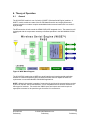
Figure 1: Wi.232FHSS Block Diagram
2.2.
•
•
•
•
•
•
•
•
•
True UART to antenna solution
16-bit CRC error checking
152.34kbit/sec maximum RF data rate
6 Hop Sequences
MAC Addressing Mode
Flexible User Addressing Mode
Link layer supports assured delivery
Small size – 0.80” x 0.935” .12” (25mW)
and 1.20” x 1.20” x 0.20” (250mW)
Low power standby, sleep and deep sleep
modes
2.3.
•
Features
•
•
•
•
•
•
•
•
PHY, MAC, and Link layer protocol built in
CSMA medium access control
120dB link budget (25mW)
130dB link budget (250mW)
Command mode for volatile and nonvolatile configuration
32-bit unique MAC address
5 volt tolerant I/O
902-928 MHz ISM band requires no license
Applications
Direct RS-232/422/485 wire
replacement (requires external RS-232
to 3V CMOS conversion circuitry)
•
RFID
•
Wireless Sensors
•
Asset Tracking
•
Remote Data Logging
•
Automated Meter Reading
•
Toys
•
Display Signs
•
Long-range data links
•
Industrial/Home Automation
Wi.232FHSS
Preliminary
© 2003-2005 Radiotronix Inc.
Preliminary
2
Preliminary
3. Table of Contents
1.
2.
Document Control................................................................................................................. 2
Introduction ........................................................................................................................... 2
2.1. Module Overview .............................................................................................................. 2
2.2. Features ............................................................................................................................ 2
2.3. Applications....................................................................................................................... 2
3.
Table of Contents ................................................................................................................. 3
4.
Table of Figures.................................................................................................................... 5
5.
Index of Tables ..................................................................................................................... 5
6.
Theory of Operation.............................................................................................................. 6
6.1. General.............................................................................................................................. 6
6.2. Operating States ............................................................................................................... 9
6.3. Addressing Modes ............................................................................................................ 9
6.3.1. MAC Mode ................................................................................................................. 9
6.3.2. User Addressing Mode ............................................................................................ 10
6.3.3. Extended User Addressing Mode ............................................................................ 11
6.3.4. Assured Delivery (Acknowledgement)..................................................................... 11
6.4. Exception Engine ............................................................................................................ 12
6.4.1. Exception Codes...................................................................................................... 12
6.4.2. Exception Masking................................................................................................... 12
6.5. Resetting Module to Factory Defaults............................................................................. 13
7.
Application Information ....................................................................................................... 14
7.1. Pin Definitions ................................................................................................................. 14
7.1.1. Wi.232FHSS-25 Pin Definitions............................................................................... 14
7.1.2. Wi.232FHSS-250 Pin Definitions............................................................................. 15
7.2. Mechanical Data ............................................................................................................. 16
7.2.1. Wi.232FHSS-25 Mechanical Drawings.................................................................... 16
7.2.2. Wi.232FHSS-250 Mechanical Drawings.................................................................. 18
7.3. Example Circuits ............................................................................................................. 20
7.4. Power Supply .................................................................................................................. 21
7.5. UART Interface ............................................................................................................... 21
7.6. Antenna ........................................................................................................................... 22
7.7. Link budget, transmit power, and range performance .................................................... 22
8.
Module Configuration.......................................................................................................... 23
8.1. Channel Hop Table ......................................................................................................... 23
8.2. Power Mode .................................................................................................................... 23
8.3. UART Data Rate ............................................................................................................. 24
8.4. Network Mode ................................................................................................................. 24
8.5. Transmit Wait Timeout .................................................................................................... 25
8.6. Maximum Transmit Retries ............................................................................................. 25
8.7. CRC Checking ................................................................................................................ 26
8.8. UART Minimum Transmission Unit................................................................................. 26
8.9. Verbose mode................................................................................................................. 26
8.10.
CSMA Enable .............................................................................................................. 26
8.11.
Operating Mode........................................................................................................... 27
8.12.
UART Acknowledgement on Wake ............................................................................. 27
8.13.
User Destination ID[3] ................................................................................................. 27
8.14.
User Destination ID[2] ................................................................................................. 28
8.15.
User Destination ID[1] ................................................................................................. 28
8.16.
User Destination ID[0] ................................................................................................. 28
8.17.
User Source ID[3] ........................................................................................................ 29
8.18.
User Source ID[2] ........................................................................................................ 29
8.19.
User Source ID[1] ........................................................................................................ 29
8.20.
User Source ID[0] ........................................................................................................ 30
8.21.
User ID Mask[3]........................................................................................................... 30
Wi.232FHSS
Preliminary
© 2003-2005 Radiotronix Inc.
Preliminary
3
Preliminary
8.22.
User ID Mask [2].......................................................................................................... 30
8.23.
User ID Mask[1]........................................................................................................... 31
8.24.
User ID Mask[0]........................................................................................................... 31
8.25.
Destination GUID[3]..................................................................................................... 31
8.26.
Destination GUID[2]..................................................................................................... 32
8.27.
Destination GUID[1]..................................................................................................... 32
8.28.
Destination GUID[0]..................................................................................................... 32
8.29.
Exception Mask ........................................................................................................... 32
8.30.
Release Number.......................................................................................................... 33
8.31.
Exception..................................................................................................................... 33
8.32.
Register Summary....................................................................................................... 34
9.
Using Configuration Registers ............................................................................................ 36
9.1. CMD Pin .......................................................................................................................... 36
9.2. CMD_RSP Pin ................................................................................................................ 36
9.3. Command Formatting ..................................................................................................... 36
9.4. Writing To Registers........................................................................................................ 37
9.5. Reading From Registers ................................................................................................. 37
10.
Electrical Specifications ...................................................................................................... 39
10.1.
Absolute Maximum Ratings......................................................................................... 39
10.2.
Detailed Electrical Specifications ................................................................................ 39
10.2.1.
AC Specifications – RX ........................................................................................ 39
10.2.2.
AC Specifications – TX ........................................................................................ 40
10.2.3.
DC Specifications ................................................................................................. 40
10.3.
Flash Specifications (Non-Volatile Registers) ............................................................. 41
11.
Custom Applications ........................................................................................................... 42
12.
Ordering Information........................................................................................................... 42
13.
Contact Us .......................................................................................................................... 42
13.1.
Technical Support........................................................................................................ 42
13.2.
Sales Support .............................................................................................................. 42
Wi.232FHSS
Preliminary
© 2003-2005 Radiotronix Inc.
Preliminary
4
Preliminary
4. Table of Figures
Figure 1: Wi.232FHSS Block Diagram ............................................................................................ 2
Figure 2: WiSE Block Diagram ........................................................................................................ 6
Figure 3: Wi.232 Networking Concept............................................................................................. 7
Figure 4: Wi.232FHSS-25 (25mW) Pin-out diagram ..................................................................... 14
Figure 5: Wi.232FHSS-250 pin-out diagram. ................................................................................ 15
Figure 6: Wi.232FHSS-25 (25mW) Module Mechanical Drawings ............................................... 16
Figure 7: Wi.232FHSS-25 (25mW) Suggested Footprint.............................................................. 17
Figure 8: Wi.232FHSS-250 (250mW) Module Mechanical Drawings ........................................... 18
Figure 9: Wi.232FHSS-250 (250mW) Suggested Footprint.......................................................... 19
Figure 10: Wi.232FHSS-250 Evaluation Module Circuit ............................................................... 20
Figure 11: Wi.232FHSS-25 Evaluation Module Circuit ................................................................. 21
Figure 12: Command and CMD Pin Timing .................................................................................. 36
Figure 13: Command Conversion Code........................................................................................ 37
5. Index of Tables
Table 1, MAC Addressing Examples............................................................................................. 10
Table 2, User Addressing Examples ............................................................................................. 10
Table 3, Extended User Addressing Examples............................................................................. 11
Table 4, Exception Codes ............................................................................................................. 12
Table 5, Example Exception Masks .............................................................................................. 12
Table 6, Module Pin Descriptions (25mW).................................................................................... 14
Table 7, Module Pin Descriptions (250mW).................................................................................. 15
Table 8, Wi.232FHSS UART Interface Lines ................................................................................ 22
Table 9, Power Mode Register Settings (25mw) .......................................................................... 24
Table 10, Data Rate Register Settings.......................................................................................... 24
Table 11, Network Mode Register Settings................................................................................... 25
Table 12, Operating Mode Register Settings ................................................................................ 27
Table 13, Release Number Register Settings ............................................................................... 33
Table 14, Release Number Register Settings ............................................................................... 34
Table 15, Volatile Read/Write Register Summary......................................................................... 34
Table 16, Non-Volatile Read-Only Register Summary.................................................................. 35
Table 17, Non-Volatile Read-Only Register Summary.................................................................. 35
Table 18, Non-Volatile Read/Write Register Summary ................................................................. 35
Table 19, Write Register Command, value to be written is less than 128 (0x80). ........................ 37
Table 20, Write Register Command, value to be written is greater than or equal to 128 (0x80). . 37
Table 21, Read Register Command .............................................................................................. 38
Table 22, Read Register Module Response For A Valid Register ................................................ 38
Table 23, Absolute Maximum Ratings........................................................................................... 39
Table 24, AC Specifications - Rx................................................................................................... 39
Table 25, AC Specifications - Tx ................................................................................................... 40
Table 26, DC Specifications .......................................................................................................... 40
Table 27, Flash Specifications (Non-Volatile Registers) ............................................................... 41
Wi.232FHSS
Preliminary
© 2003-2005 Radiotronix Inc.
Preliminary
5
Preliminary
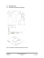
6. Theory of Operation
6.1.
General
The Wi.232FHSS module is one of a family of WiSE™ (Wireless Serial Engine) modules. A
WiSE™ module combines a state-of-the-art FSK data transceiver and a high-performance
protocol controller to create a complete embedded wireless communications link in a small ICstyle package.
The RF transceiver is built around the XEMICS XE1203F integrated circuit. The transceiver will
be designed with the components necessary to facilitate operation in the 902-928MHz US ISM
band
Figure 2: WiSE Block Diagram
The Wi.232FHSS module has a UART-type serial interface and contains special application
software to create a transparent UART-to-antenna wireless solution capable of direct wire
replacement in most embedded RS-232/422/485 applications.
NOTE: Although the module is capable of supporting the typical serial communications required
by RS-232, RS-422, and RS-485 networks, it is not compatible with the electrical interfaces for
these types of networks. The module has CMOS inputs and outputs and would require an
appropriate converter for the particular type of network it is connected to.
Wi.232FHSS
Preliminary
© 2003-2005 Radiotronix Inc.
Preliminary
6
Preliminary
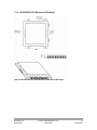
Figure 3: Wi.232 Networking Concept
The module is designed to interface directly to a host UART. Three signals are used to transfer
data between the module and the host UART: TXD, RXD, and CTS. TXD is the data output from
the module RXD is the data input to the module. CTS is an output that indicates the status of the
module’s data interface. If CTS is low, the module is ready to accept data. If CTS is high, the
module is busy and the host UART should not send any further data. The UART interface is
capable of operating in full duplex at baud rates from 2.4 to 115.2 kbps.
Internally, the module has a 256 byte buffer for incoming characters from the host UART. The
module can be programmed to automatically transmit when the buffer reaches a programmed
limit, set by regUARTMTU. The module can also be programmed to transmit based on a delay
between characters, set by regTXTO (set in 1mSec increments). These registers allow the
designer to optimize performance of the module for fixed length and variable length data. The
module supports streaming data, as well. To optimize the module for streaming data,
regUARTMTU should be set to 144, and regTXTO should be set to a value equal to 1 UART byte
time (10 bit times rounded up) at the current UART data rate plus one. If the buffer is full, or the
timer set by regTXTO expires, and the module is in the process of sending the previous packet
over the RF link, the module will assert CTS high, indicating that the host should not send any
more data. Data sent by the host while CTS is high will be lost. When there is data in the UART
receive/RF Transmit buffer, the BE pin is low; when this buffer is empty, BE is high.
When the MAC layer has a packet to send, it will optionally use a carrier-sense-multiple-access
(CSMA) protocol to determine if another module is already transmitting. If another module is
transmitting, the module will receive that data before attempting to transmit its data again. If,
during this process, the UART receive buffer gets full, the CTS line will go high to prevent the host
UART from over-running the receive buffer. The CSMA mechanism introduces a variable delay
to the transmission channel. This delay is the sum of a random period and a weighted period that
is dependent on the number of times that the module has tried and failed to acquire the channel.
For applications that guarantee that only one module will be transmitting at any given time, the
CSMA mechanism can be turned off to avoid this delay.
Wi.232FHSS
Preliminary
© 2003-2005 Radiotronix Inc.
Preliminary
7
Preliminary
The MAC layer prefixes the data with a packet header and postfixes the data with a 16-bit CRC.
The CRC-16 packet validation can be disabled to allow the application to do its own error
checking.
The Link layer provides three distinct addressing modes: MAC, User, and User Extended. Each
of these addressing modes can be configured to utilize assured (acknowledged) or best-effort
(not acknowledged) delivery. MAC addressing mode is best suited for point-to-point or broadcast
transmissions. User and User Extended modes, with their address masks, allow for the creation
of subnets.
The Wi.232FHSS is very flexible because of its extensive configurability. However, modules that
are not configured in the same way will not be able to communicate reliably, causing poor
performance or outright failure of the wireless link. All modules in a network must have
compatible configurations to ensure interoperability.
In TRANSMIT mode, the transceiver has a complete packet queued for transmission. The
module uses the same CSMA mechanism to arbitrate access to the channel. Once the module
gains access to the channel, the packet is transmitted on the current channel without delay. If
BIT_ACK or REG_NETWORKMODE is set, the module starts TO_ACKWAIT and begins waiting
for an ACK from the other side. If the ACK is not received, a transmission retry is attempted. If
the number of transmission retries exceeds REG_MAXTXRETRY, an exception (EX_NORFACK)
is raised.
Once the packet is sent, the transmitter will remain on the current channel until its hop time has
expired. If another packet is queued for transmission, the module will transmit this packet once
the CSMA mechanism regains access to the channel. Once the hop timer has expired, the
module will then hop to the next channel (both transmit and receive channels). The module will
remain synchronized until it dwells for one full hop time without transmitting or receiving a packet.
The module will then return to scan mode.
Certain features of the module are controlled through programmable registers. Registers are
access by bringing CMD low. When CMD is low, all data transfers from the host UART are
considered to be register access commands. When CMD is high, all data transfers from the host
UART are considered to be raw data that needs to be transparently transmitted across the
wireless link. The module maintains two copies of each register: one in flash and one in RAM.
On reset, the module loads the RAM registers from the values in the flash registers. The module
is operated out of the RAM registers. Applications that need to change parameters of the module
often would simply modify the RAM register. By putting default settings in the flash registers, the
module will always power up in a preconfigured state, which is useful for applications that do not
have external microcontrollers, such as RS-232 adapters.
The FHSS module has 32 channels spaced on 750kHz boundaries with guard bands on either
side. These channels are pseudo-randomly arranged into six unique hopping tables comprised of
26 channels. The order of these tables is chosen so that cross-correlation is minimized, allowing
multiple networks to operate in proximity with minimal interference.
In the SLEEP and DEEP SLEEP modes, the transceiver is powered down and will not
synchronize with other modules. SLEEP mode draws more current than DEEP SLEEP mode. In
DEEP SLEEP mode the module draws the least current. To wake the module up from this mode
the C2CK/RST pin must be held low for at least 15µs and then return it high. Modules do not
monitor the receive channel in either SLEEP or DEEP SLEEP mode. Therefore, it is impossible
to remotely wake a sleeping module via the RF interface.
Wi.232FHSS
Preliminary
© 2003-2005 Radiotronix Inc.
Preliminary
8
Preliminary
6.2.
Operating States
The primary active state is the RX SCAN state. When the module is not actively transmitting or
receiving data, it is in this state. It is cycling from one channel to another throughout the hop
sequence looking for a synchronizing packet. If the module detects a pre-amble, it will stall the
next hop to wait for the start-code and packet header. If the packet is addressed for it, the
module will process the packet and present it to the UART for transmission to the host
microprocessor. If not, it will resume scanning for another master.
Once the UART has buffered enough data to send (either regUARTMTU bytes received or
regTXTO has expired), it will schedule a transmission with the RF layer. The RF layer will make
a best-effort attempt to keep the data in at least regUARTMTU-sized packets, but will split data to
better fill the communications channel if the hop time allows.
6.3.
Addressing Modes
The Wi.232FHSS module has a very flexible addressing scheme incorporated into its firmware.
The addressing modes can be dynamically changed as the module operates. Selection of the
addressing mode is made through the regNVNETWORKMODE and regNETWORKMODE
registers. Selection of an addressing mode forces the transmitter to address packets according
to this configuration. When receiving, a module will receive and process all addressing types,
regardless of regNETWORKMODE configuration. If the received message matches the
addressing criteria, it will be passed through to the UART for transmission to the host processor.
6.3.1. MAC Mode
MAC mode supports point to point and broadcast communications. In this mode, endpoint
addressing is accomplished through the regNVDESTGUID[3-0] and regDESTGUID[3-0] registers.
The module’s source GUID (regMYGUID[3-0]) is fixed and locked at the factory. MAC
addressing mode is selected by writing either 0x04 (MAC) or 0x14 (MAC w/ acknowledgement) to
the regNETWORKMODE register. A destination GUID of 0xFFFFFFFF causes the module to
send broadcast messages- all modules within range will receive and process these messages. A
module will only process a MAC message if the message’s destination address is 0xFFFFFFFF
or it exactly matches its regMYGUID[3-0] address. Acknowledgement is enabled by setting bit 4
of regNETWORKMODE. The following table lists some examples of how MAC addressing works.
Wi.232FHSS
Preliminary
© 2003-2005 Radiotronix Inc.
Preliminary
9
Preliminary
NetworkMode
Sender
MyGUID
DestinationGUID
0x04
0x00001000
0xFFFFFFFF
0x14
0x00001000
0xFFFFFFFF
0x14
0x00001000
0x00003000
MyGUID
0x00002000
0x00003000
0x00002000
0x00003000
0x00002000
0x00003000
0x04
0x00001000
0x00002000
0x00002000
0x00003000
Receiver
Response
Data sent to UART. No RF
ACK sent by either module.
Data sent to UART. No
ACK sent by either module.
This configuration will
cause transmission
problems.
Not processed- discarded.
Data sent to UART. RF
ACK sent to 0x00001000.
Data sent to UART. No RF
ACK sent.
Not processed- discarded.
Table 1, MAC Addressing Examples
6.3.2. User Addressing Mode
When user network mode is selected, transmitted packets locate endpoints using the customer ID
and destination user ID (specified in regCUSTID[1-0] and regUSERDESTID[1-0], respectively).
On the receiving side, each module has a User ID mask (regUSERIDMASK[1..0]) that it applies
to both its own user id (regUSERSRCID[1-0]) and the incoming destination User ID. Once both
are masked, if the results are equal, the receiving module will pass the payload data to the
application for presentation to the host. Additionally, if the incoming address, once masked,
equals the mask itself, its payload will be presented to the host. If an acknowledgement is
requested, the receiving module will respond only if the unmasked user ids are equal. When
using user network mode to send packets to multiple users (mask not equal to 0xFFFF), assured
delivery must be disabled. Failure to do so could cause extreme delays in transmission and loss
of data. The following table shows some examples of user addressing at work.
Network
Mode
Sender
User
User
SRCID DESTID
User SRCID
0x06
0x1000
0xFFFF
0x2000
0x3000
User
IDMASK
0xFFFF
0xFFFF
0x2000
0xFFFF
0x16
0x1000
0xFFFF
0x3000
0xFFFF
0x2000
0xE000
0x3000
0xE000
0x2000
0xF000
0x3000
0xF000
0x16
0x06
0x1000
0x1000
Receiver
Response
0x3000
0x3000
Data sent to UART. No RF
ACK sent by either module.
Data sent to UART in both
modules. No ACK sent by
either module. This
configuration will cause
transmission problems.
Data sent to UART. No RF
ACK sent.
Data sent to UART. RF ACK
sent to 0x1000 by GUID.
Not processed- discarded.
Data sent to UART. No RF
ACK sent.
Table 2, User Addressing Examples
Wi.232FHSS
Preliminary
© 2003-2005 Radiotronix Inc.
Preliminary
10
Preliminary
6.3.3. Extended User Addressing Mode
When extended user network mode is selected, transmitted packets locate endpoints using the
customer ID and destination user ID (specified in regCUSTID[1-0] and regUSERDESTID[3-0],
respectively). On the receiving side, each module has a User ID mask (regUSERIDMASK[3-0])
that it applies to both its own user id (regUSERSRCID[3-0]) and the incoming destination User ID.
Once both are masked, if the results are equal, the receiving module will pass the payload data to
the application for presentation to the host. Additionally, if the incoming address, once masked,
equals the mask itself, its payload will be presented to the host. If an acknowledgement is
requested, the receiving module will respond only if the unmasked user ids are equal. When
using extended user network mode to send packets to multiple users (mask not equal to
0xFFFFFFFF), assured delivery must be disabled. Failure to do so could cause extreme delays
in transmission and loss of data. The following table shows some examples of extended user
addressing at work.
Network
Mode
0x07
0x17
0x17
0x07
Sender
User SRCID
User DESTID
User SRCID
0x10000000
0xFFFFFFFF
0x20000001
0x20000002
User
IDMASK
0xFFFFFFFF
0xFFFFFFFF
0x20000001
0xFFFFFFFF
0x20000002
0xFFFFFFFF
0x20000001
0xE0000000
0x30000001
0xE0000000
0x20000001
0xF0000000
0x30000001
0xF0000000
0x10000000
0x10000000
0x10000000
Receiver
Response
0xFFFFFFFF
0x30000001
0x30000002
Data sent to UART. No RF
ACK sent by either module.
Data sent to UART in both
modules. No ACK sent by
either module. This
configuration will cause
transmission problems.
Data sent to UART. No RF
ACK sent.
Data sent to UART. RF ACK
sent to 0x10000000 by GUID.
Not processed- discarded.
Data sent to UART. No RF
ACK sent.
Table 3, Extended User Addressing Examples
6.3.4. Assured Delivery (Acknowledgement)
While not an addressing mode on its own, assured delivery can be enabled for each of the above
addressing modes. When a module transmits with assured delivery enabled, it obligates the
receiving module to return an acknowledgement packet. The transmitting module will wait for this
acknowledgement for a preset amount of time based on the data rate. If acknowledgement is not
received, it will retransmit the current packet. If the receiver receives more than one of the same
packet, it will discard the packet contents but send an acknowledgment. This way, duplicate data
is not presented to the receiver’s UART. It is extremely important that assured delivery be used
only when the unmasked user/extended user destination ID or Destination GUID points to a
specific module. Failure to specifically address a valid endpoint could cause the module to
appear slow or unresponsive due to repeated retransmissions. This will also serve to congest the
network, impeding valid communications. Assured delivery is enabled by setting bit 4 of
REG_NETWORKMODE.
TROUBLESHOOTING HINT: Communications Problems. If you are unable to communicate
with another module, it is most likely one of a couple of things. First, check to make sure that you
are using the same data rate. Modules programmed to different data rates will not communicate
Wi.232FHSS
Preliminary
© 2003-2005 Radiotronix Inc.
Preliminary
11
Preliminary
nor share the RF channel with one another. Second, ensure that your network mode and
addressing is configured to properly access the module of interest. Also, ensure that you are
addressing a specific module when using acknowledgment. Failure to do so will cause large
delays and loss of data.
6.4.
Exception Engine
Wi.232FHSS modules are equipped with an internal exception engine. When errors occur during
module operation, an exception is raised. Exception codes are stored in the regEXCEPTION
register when they occur and cleared once they are read. If an exception code is already present
in regEXCEPTION following an error, the new exception code will overwrite the old one.
6.4.1. Exception Codes
Exception codes are organized by type for ease of masking (see Exception Masking). The
following table lists the exception codes and their meanings. All other values are reserved.
Exception
Code
0x08
0x09
0x13
0x20
Exception Name
Description
EX_BUFOVFL
EX_RFOVFL
EX_WRITEREGFAILED
EX_NORFACK
0x40
0x42
0x43
0x44
EX_BADCRC
EX_BADHEADER
EX_BADSEQID
EX_BADFRAMETYPE
Internal UART buffers overflowed
Internal RF packet buffer overflowed
Attempted write to register failed
Acknowledgement packet not received after
maximum number of retries
Bad CRC detected on incoming packet
Bad CRC detected in packet header
Sequence ID was incorrect in ACK packet
Unsupported frame type specified
Table 4, Exception Codes
6.4.2. Exception Masking
Wi.232FHSS modules have an external pin, EX, that can be asserted to indicate to the host that
an error has occurred. The exception mask provides a simple method of discriminating which
errors cause the EX pin to toggle. If the exception code, once anded with the exception mask
(regEXCEPTIONMASK), is non-zero, the EX pin is asserted. Once the EX pin is asserted, the
regEXCEPTION register must be read to return it to low. The following table lists some example
exception masks.
Exception
Mask
0x08
0x10
0x20
0x40
0x60
0xFF
Exception Name
Allows only EX_BUFOVFL and EX_RFOVFL to trigger the EX pin
Allows only EX_WRITEREGFAILED to trigger the EX pin
Allows only EX_NORFACK to trigger the EX pin
Allows only EX_BADCRC, EX_BADHEADER, EX_BADSEQID, and
EX_BADFRAMETYPE exceptions to trigger the EX pin
Allows EX_BADCRC, EX_BADHEADER, EX_BADSEQID, EX_BADFRAMETYPE,
and EX_NORFACK exceptions to trigger the EX pin
Allows all exceptions to trigger the EX pin
Table 5, Example Exception Masks
Wi.232FHSS
Preliminary
© 2003-2005 Radiotronix Inc.
Preliminary
12
Preliminary
6.5.
Resetting Module to Factory Defaults
It may be necessary to reset the non-volatile registers to their factory defaults. To reset the
module to factory defaults, hold the command line low and cycle power to the module. The
command line must remain low for a minimum of 600ms after the resetting the module. Once the
command line is released, the module’s non-volatile registers will be reset to factory defaults.
Wi.232FHSS
Preliminary
© 2003-2005 Radiotronix Inc.
Preliminary
13
Preliminary
7. Application Information
7.1.
Pin Definitions
7.1.1. Wi.232FHSS-25 Pin Definitions
Figure 4: Wi.232FHSS-25 (25mW) Pin-out diagram
No.
1
2
3
4
5
6
7
8
9
10
11
12
13
14
15
16
17
18
19
Pin Definitions
Description
Ground
Exception Output
Buffer Empty
Command input – active low
UART receive input
UART transmit output
UART clear to send output – active low
Command Response indication
Analog RSSI
Reserved – ISP pin
ISP pin/Wake from DEEP SLEEP/Module Reset
Ground
Antenna port – 50 ohm
Ground
Ground
Ground
Ground
Ground
VCC – 2.7 to 3.6 VDC
Table 6, Module Pin Descriptions (25mW)
Legend
Signals that are used in this implementation
Signals used for in-system programming
Wi.232FHSS
Preliminary
© 2003-2005 Radiotronix Inc.
Preliminary
14
Preliminary
7.1.2. Wi.232FHSS-250 Pin Definitions
Figure 5: Wi.232FHSS-250 pin-out diagram.
No.
1
2
3
4
5
6
7
8
9
10
11
12
13
14
15
16
17
18
19
20
21
22
23
24
25
26
Pin Definitions
Description
No connect – reserved
UART Transmit output
No connect - reserved
No connect – reserved
No connect – reserved
ISP pin / Wake from deep sleep/Module Reset
Reserved – ISP pin
No connect – reserved
Command Response indication – low when UART output is a command response
Exception Output, maskable. Cleared on exception read.
Ground
Ground
Ground
RSSI
Command Mode select – active low
Buffer Empty – high when input buffer is empty
N/C
UART Request To Send input – not currently implemented (reserved)
UART Clear To Send output – active low
UART Receive input
Ground
Antenna Port – 50 ohms
Ground
VCC
VCC
VCC
Table 7, Module Pin Descriptions (250mW)
Legend
Signals that are used in this implementation
Signals used for in-system programming
Wi.232FHSS
Preliminary
© 2003-2005 Radiotronix Inc.
Preliminary
15
Preliminary
7.2.
Mechanical Data
7.2.1. Wi.232FHSS-25 Mechanical Drawings
Figure 6: Wi.232FHSS-25 (25mW) Module Mechanical Drawings
Wi.232FHSS
Preliminary
© 2003-2005 Radiotronix Inc.
Preliminary
16
Preliminary
Figure 7: Wi.232FHSS-25 (25mW) Suggested Footprint
Wi.232FHSS
Preliminary
© 2003-2005 Radiotronix Inc.
Preliminary
17
Preliminary
7.2.2. Wi.232FHSS-250 Mechanical Drawings
Figure 8: Wi.232FHSS-250 (250mW) Module Mechanical Drawings
Wi.232FHSS
Preliminary
© 2003-2005 Radiotronix Inc.
Preliminary
18
Preliminary
Figure 9: Wi.232FHSS-250 (250mW) Suggested Footprint
Wi.232FHSS
Preliminary
© 2003-2005 Radiotronix Inc.
Preliminary
19
Preliminary
7.3.
Example Circuits
Figure 10: Wi.232FHSS-250 Evaluation Module Circuit
Wi.232FHSS
Preliminary
© 2003-2005 Radiotronix Inc.
Preliminary
20
Preliminary
Figure 11: Wi.232FHSS-25 Evaluation Module Circuit
7.4.
Power Supply
Although the Wi.232FHSS module is very easy to use, care must be given to the design of the
power supply circuit. It is important for the power supply to be free of digital noise generated by
other parts of the application circuit, such as the RS-232 converter.
Figure 11 shows the schematic for our evaluation module circuit for the Wi.232FHSS-25 and
Wi.232FHSS-250 modules. The EVM includes an on-board power supply and antenna
connector. These evaluation circuits were used to measure the performance of the Wi.232FHSS
module, and should be used as a reference for Wi.232FHSS based designs.
If noise is a problem, it can usually be eliminated by using a dedicated LDO regulator for the
module and/or by separating the grounds for the module and the other circuits.
Additionally, power supply rise time is extremely important. The power supply presented to the
module must rise from Vss to 2.7V in less than 1ms. If this specification cannot be met, an
external reset supervisor circuit must be used to hold the module in reset until the power supply
stabilizes. Failure to ensure adequate power supply rise time can result in loss of
important module configuration information.
7.5.
UART Interface
The UART interface is very simple; it is comprised of four CMOS compatible digital lines.
Wi.232FHSS
Preliminary
© 2003-2005 Radiotronix Inc.
Preliminary
21
Preliminary
Line
Direction
Description
CTS
Out
Clear to send – this pin indicates to the host micro when it is ok to send data.
When CTS is high, the host micro should stop sending data to the module until
CTS returns to the low state.
CMD
In
Command – the host micro will bring this pin low to put the module in
command mode. Command mode is used to set and read the internal
registers that control the operation of the module. When CMD is high,
the module will transparently transfer data to and from other modules
on the same channel.
RXD
TXD
In
Out
NOTE: If this pin is low when the module comes out of reset, the registers will
be reset to their factory programmed defaults. It is important to ensure that
CMD is held high during power-up.
Receive data input.
Transmit data output
Table 8, Wi.232FHSS UART Interface Lines
7.6.
Antenna
The module is designed to work with any 50-ohm antenna, including PCB trace antennas.
We are often asked: “What is the best antenna to use with your module?” Actually, the selection
of an antenna is based on a particular application, not the module used.
As a rule, a ¼ wave whip antenna with a good, solid ground plane is an excellent choice.
However, many embedded applications cannot support an externally mounted antenna. If this is
the case, a PCB antenna must be used. The designer can either use an off-of-the-shelf PCB
antenna, such as the Splatch from Linx Technologies, or design a trace antenna. There are
several good antenna tutorials and references on the Internet and we encourage the designer to
use these resources.
Note: Antenna design is difficult and can be impossible without the proper test equipment. As
such, we strongly encourage all of our customers to use off-of-the-shelf antennas whenever
possible.
7.7.
Link budget, transmit power, and range performance
A link budget is the best figure of merit for comparing wireless solutions and determining how
they will perform in the field.
In general, the solution with the best link budget will deliver the best line-of-sight range
performance. Improving the link budget by increasing the receiver sensitivity will result in lower
power consumption while improving the link budget by increasing the transmit power will result in
more robust performance in the presence of an on-channel interferer or multi-path interference.
Wireless Fact: You will never reduce the performance of a wireless link by increasing the
sensitivity.
It has been proposed that less sensitive receivers will perform better in a noisy environment. That
simply is not true. It is the equivalent of saying that someone who is hard of hearing can hear
better in a noisy room than in a quiet room. The real solution is to make the talker speak louder
to get over the noise in the room. The same is true for a wireless link. In real-world, noisy
environments, increased output power is generally the best way to improve range performance.
To calculate the link budget for a wireless link, simply add the transmit power, the antenna gains,
and the receiver sensitivity:
Wi.232FHSS
Preliminary
© 2003-2005 Radiotronix Inc.
Preliminary
22
Preliminary
LB = Ptx + Gtxa − SENSrx + Grxa
For example, the link budget for a pair of 25mW Wi.232FHSS modules at the maximum data rate
and using 3dBi whips antennas would be:
(25mW): +14dBm + 3dB – (-100dBm) + 3dB: 120dB
(250mW): +24dBm + 3dB – (-100dBm) + 3dB: 130dB
A link budget of 120dB should easily yield a range of 1/2 mile or more outdoors. If the
environment is open and the antennas are 8 to 10 feet off of the ground, the range could be a
mile. Indoors, this link budget should yield a range of several hundred feet.
This is a well-balanced link budget. More than 10dB of the budget is achieved through transmit
power, which will allow good performance indoors in the presence of multi-path while keeping the
overall operating current low, making the module suitable for primary battery powered
applications such as RFID and automated meter reading.
8. Module Configuration
The Wi.232FHSS modules will work right “out of the box” without any configuration. However, a
great many configuration registers are exposed to allow for the custom-tailoring of the wireless
link. These registers are classified as four different types: non-volatile R/W, non-volatile R/O,
volatile R/W, and volatile R/O. During the power-on/reset sequence, the non-volatile read/write
are copied into the volatile read/write registers. This allows the integrator to determine a default
configuration for the wireless link that can be preset at the factory, requiring no intervention by the
host processor. During operation, changes to the volatile read/write registers have an immediate
effect on the Wi.232FHSS parameters. Non-volatile read-only registers provide a way for the
host application to retrieve information about the module hardware, firmware, and hard-coded
configuration parameters such as the MyGUID address. There is currently only one volatile readonly register- regEXCEPTION. Refer to the Exception Engine section for more information.
8.1.
Channel Hop Table
regNVHOPTABLE(0x00)
R/W
R/W
R/W
RES
D6
D5
7
6
5
R/W
D4
4
R/W
D3
3
regHOPTABLE (0x4B)
R/W
R/W
R/W
D2
D1
D0
2
1
0
Default hop sequence: 0
The Wi.232FHSS supports 6 different hop sequences with minimal correlation. Changing the hop
sequence changes the physical band utilization, much the same way that a channel does in a
static transmitter. Valid values are 0-5.
8.2.
Power Mode
regNVPWRMODE (0x02)
R/W
R/W
R/W
NA
NA
NA
7
6
5
R/W
NA
4
R/W
NA
3
regPWRMODE (0x4D)
R/W
R/W
R/W
NA
PM1
PM0
2
1
0
Default Power Mode: High Power
Wi.232FHSS
Preliminary
© 2003-2005 Radiotronix Inc.
Preliminary
23
Preliminary
The power mode setting is not configurable in the Wi.232FHSS-250. For the Wi.232FHSS-25,
the following table applies:
PM1
0
0
1
1
PM0
0
1
0
1
Mode
Low
Med-Low
Med High
High (DEFAULT)
Table 9, Power Mode Register Settings (25mw)
8.3.
UART Data Rate
regNVUARTDATARATE (0x03)
R/W
R/W
R/W
RES
RES
RES
7
6
5
R/W
RES
4
R/W
RES
3
regUARTDATARATE (0x4E)
R/W
R/W
R/W
BR2
BR1
BR0
2
1
0
Default UART Data Rate: 2400 baud
Changing the value in regNVUARTDATARATE will change the default data rate at power-on.
Changing regUARTDATARATE will change the current data rate. Before the module switches
data rates, it will send a UART acknowledge at the current setting. Valid settings are:
Baud Rate
2400
9600
19200
38400
57600
115200
10400
31250
BR2
0
0
0
0
1
1
1
1
BR1
0
0
1
1
0
0
1
1
BR0
0
1
0
1
0
1
0
1
Table 10, Data Rate Register Settings
TROUBLESHOOTING HINT: Baud Rate Problems. If you lose track of the baud rate setting of
the module, it will be impossible to program the module. You can either try every possible baud
rate to discover the setting, or force a power-on reset with CMD held low to set the baud rate to
its default: 2.4kbit/second.
8.4.
Network Mode
regNVNETWORKMODE (0x04)
R/W
R/W
R/W
D7
D6
D5
7
6
5
R/W
D4
4
R/W
D3
3
regNETWORKMODE (0x4F)
R/W
R/W
R/W
D2
D1
D0
2
1
0
Default Network Mode: MAC Mode
The module supports three distinct networking modes: MAC, USER, and Extended USER. For
each of these modes, assured delivery (acknowledgement) can be either enabled or disabled.
For more information, see Addressing Modes section of this manual. Valid settings are:
Wi.232FHSS
Preliminary
© 2003-2005 Radiotronix Inc.
Preliminary
24
Preliminary
Network Mode
0x04
0x05
0x06
0x07
0x14
0x15
0x16
0x17
Meaning
MAC Address Mode
Reserved
User Address Mode
User Extended Address Mode
MAC Address Mode with Acknowledgement
Reserved
User Address Mode with Acknowledgement
Extended User Address Mode with Acknowledgement
Table 11, Network Mode Register Settings
All other network modes are reserved and may cause undesired operation.
TROUBLESHOOTING HINT: Communications Problems. If you are unable to communicate
with another module, it is most likely one of a couple of things. First, check to make sure that you
are using the same data rate. Modules programmed to different data rates will not communicate
nor share the RF channel with one another. Second, ensure that your network mode and
addressing is configured to properly access the module of interest. Also, ensure that you are
addressing a specific module when using acknowledgment. Failure to do so will cause large
delays and loss of data.
8.5.
R/W
D7
7
Transmit Wait Timeout
regNVTXTO (0x05)
R/W
R/W
D6
D5
6
5
R/W
D4
4
R/W
D3
3
R/W
D2
2
regTXTO (0x50)
R/W
R/W
D1
D0
1
0
Default Transmit Wait Timeout: 16ms
When a byte is received by the UART, the module will start a timer that will countdown every
millisecond. The timer is restarted each time a byte is received by the UART. If the timer
reaches zero before the next byte is received from the UART, the module will schedule a
transmission with the RF interface. Normally, this timeout value should be 0x02 or greater than
one byte time at the current UART data rate. If the timeout value is set to 0x00, the transmit wait
timeout will not operate, and a minimum of regUARTMTU bytes will be required for transmission.
The default setting for this register is 0x10 (15-16ms delay).
8.6.
Maximum Transmit Retries
regNVMAXTXRETRY(0x07)
R/W
R/W
R/W
D7
D6
D5
7
6
5
R/W
D4
4
R/W
D3
3
regMAXTXRETRY (0x52)
R/W
R/W
R/W
D2
D1
D0
2
1
0
Default Maximum Transmit Retries: 26
Sets the number of transmission tries if an acknowledgement is not received. If an
acknowledgement is not received, EX_NORFACK is raised.
Wi.232FHSS
Preliminary
© 2003-2005 Radiotronix Inc.
Preliminary
25
Preliminary
8.7.
CRC Checking
regNVUSECRC (0x08)
R/W
R/W
R/W
B7
B6
B5
7
6
5
R/W
B4
4
R/W
B3
3
R/W
B2
2
regUSECRC (0x53)
R/W
R/W
B1
B0
1
0
Default CRC Checking: Enabled (0x01)
Set to 0x01 to enable receiver CRC-16 validation, or 0x00 to disable. The default CRC mode
setting is enabled.
8.8.
UART Minimum Transmission Unit
regNVUARTMTU (0x09)
R/W
R/W
R/W
B7
B6
B5
7
6
5
R/W
B4
4
R/W
B3
3
regUARTMTU (0x54)
R/W
R/W
R/W
B2
B1
B0
2
1
0
Default UART Minimum Transmission Unit: 64
This register determines the UART buffer level that will trigger the transmission of a packet. The
minimum value is 1 and the maximum value is 192. The default value for this register is 64,
which provides a good mix of throughput and latency. At maximum data rate, a value of 144 will
optimize throughput.
8.9.
Verbose mode
regNVSHOWVERSION (0x0A)
R/W
R/W
R/W
B7
B6
B5
7
6
5
R/W
B4
4
R/W
B3
3
regSHOWVERSION (0x55)
R/W
R/W
R/W
B2
B1
B0
2
1
0
Default Verbose Mode: Enabled (0x01)
Setting this register to 0x00 will suppress the start-up message, including firmware version, that is
sent to the UART when the module is reset. A value of 0x01 will cause the message to be
displayed after reset. By default, the module start-up message will be displayed. The nonvolatile counterpart, regSHOWVERSION, has no function.
8.10. CSMA Enable
regNVCSMAMODE (0x0B)
R/W
R/W
R/W
B7
B6
B5
7
6
5
R/W
B4
4
R/W
B3
3
regCSMAMODE (0x56)
R/W
R/W
R/W
B2
B1
B0
2
1
0
Default CSMA Enable: Enabled (0x01)
Carrier-sense multiple access (CSMA) is a best-effort delivery system that listens to the channel
before transmitting a message. If another Wi.232 module is already transmitting when a
message is queued, the module will wait before sending its payload. This helps to eliminate RF
Wi.232FHSS
Preliminary
© 2003-2005 Radiotronix Inc.
Preliminary
26
Preliminary
message corruption at the expense of additional latency. Setting this register to 0x01 will enable
CSMA. Setting this register to 0x00 will disable CSMA. By default, CSMA is enabled.
8.11. Operating Mode
regNVOPMODE (0x0D)
R/W
R/W
R/W
B7
B6
B5
7
6
5
R/W
B4
4
R/W
B3
3
R/W
B2
2
regOPMODE (0x58)
R/W
R/W
B1
B0
1
0
Default Operating mode: Awake (0x00)
Changing this register will place the register in the following operating modes:
Operating Mode
Awake
Sleep
Standby
Deep Sleep
B1
0
0
1
1
B0
0
1
0
1
Table 12, Operating Mode Register Settings
8.12. UART Acknowledgement on Wake
regNVACKONWAKE (0x0E)
R/W
R/W
R/W
D7
D6
D5
7
6
5
R/W
D4
4
R/W
D3
3
regACKONWAKE (0x59)
R/W
R/W
R/W
D2
D1
D0
2
1
0
Default UART Acknowledgement on Wake: Enabled (0x01)
When UART Acknowledge on Wake is enabled, the module will send an ACK (0x06) character
out of the UART after the module wakes. This indicates that the module is ready to accept traffic.
A value of 0x01 enables this feature. Setting the register to 0x00 disables it.
8.13. User Destination ID[3]
regNVUSERDESTID[3] (0x0F)
R/W
R/W
R/W
D7
D6
D5
7
6
5
R/W
D4
4
R/W
D3
3
regUSERDESTID[3] (0x5A)
R/W
R/W
R/W
D2
D1
D0
2
1
0
Default User Destination ID[3]: 0xFF
This is the most significant byte (byte 3) of the 32-bit user extended destination address. When
Extended User addressing is enabled, this register is used in conjunction with User Destination
Address[2-0] registers to direct a transmitted packet to the proper endpoint(s).
Wi.232FHSS
Preliminary
© 2003-2005 Radiotronix Inc.
Preliminary
27
Preliminary
8.14. User Destination ID[2]
regNVUSERDESTID[2] (0x10)
R/W
R/W
R/W
D7
D6
D5
7
6
5
R/W
D4
4
R/W
D3
3
regUSERDESTID[2] (0x5B)
R/W
R/W
R/W
D2
D1
D0
2
1
0
Default User Destination ID[2]: 0xFF
This is byte 2 of the 32-bit user extended destination address. When Extended User addressing
is enabled, this register is used in conjunction with User Destination ID[3] and User Destination
ID[1-0] registers to direct a transmitted packet to the proper endpoint(s).
8.15. User Destination ID[1]
RegNVUSERSRCID[1] (0x11)
R/W
R/W
R/W
D7
D6
D5
7
6
5
R/W
D4
4
R/W
D3
3
regNVUSERSRCID[1] (0x5C)
R/W
R/W
R/W
D2
D1
D0
2
1
0
Default User Destination ID[1]: 0xFF
When user-extended addressing is selected, this is byte 1 of the 32-bit user-extended destination
address; when user addressing is selected, it is the most significant byte of the user destination
address. When extended-user addressing is selected, this register is used in conjunction with
User Destination ID[3-2] and User Destination ID[0] registers to direct a transmitted packet to the
proper endpoint(s). When user addressing is selected, this register is used in conjunction with
the User Destination ID[0] register to direct a transmitted packet to the proper endpoint(s).
8.16. User Destination ID[0]
RegNVUSERSRCID[0] (0x12)
R/W
R/W
R/W
D7
D6
D5
7
6
5
R/W
D4
4
R/W
D3
3
regNVUSERSRCID[0] (0x5D)
R/W
R/W
R/W
D2
D1
D0
2
1
0
Default User Destination ID[0]: 0xFF
When user-extended addressing is selected, this is the least significant byte of the 32-bit
extended-user destination address; when user addressing is selected, it is the least significant
byte of the user destination address. When user-extended addressing is selected, this register is
used in conjunction with User Destination Address[3-1] registers to direct a transmitted packet to
the proper endpoint(s). When user addressing is selected, this register is used in conjunction
with the User Destination Address[1] register to direct a transmitted packet to the proper
endpoint(s).
Wi.232FHSS
Preliminary
© 2003-2005 Radiotronix Inc.
Preliminary
28
Preliminary
8.17. User Source ID[3]
regNVUSERSRCID[3] (0x13)
R/W
R/W
R/W
D7
D6
D5
7
6
5
R/W
D4
4
R/W
D3
3
regUSERSRCID[3] (0x5E)
R/W
R/W
R/W
D2
D1
D0
2
1
0
Default User Source ID[3]: 0xFF
When user-extended addressing is selected, this register holds the most significant byte (byte 3)
of the 32-bit user-extended source address. When Extended User addressing is invoked, this
register is used in conjunction with User Source Address[2-0] registers to make up the module’s
32-bit user-extended source address.
8.18. User Source ID[2]
regNVUSERSRCID[2] (0x14)
R/W
R/W
R/W
D7
D6
D5
7
6
5
R/W
D4
4
R/W
D3
3
regUSERSRCID[2] (0x5F)
R/W
R/W
R/W
D2
D1
D0
2
1
0
Default User Source ID[2]: 0xFF
When user-extended addressing is selected, this register holds byte 2 of the 32-bit user-extended
source address. When Extended User addressing is invoked, this register is used in conjunction
with User Source Address [3] and User Source Address [1-0] registers to make up the module’s
32-bit extended-user source address.
8.19. User Source ID[1]
regNVUSERSRCID[1] (0x15)
R/W
R/W
R/W
D7
D6
D5
7
6
5
R/W
D4
4
R/W
D3
3
regUSERSRCID[1] (0x60)
R/W
R/W
R/W
D2
D1
D0
2
1
0
Default User Source ID[1]: 0xFF
When user-extended addressing is selected, this register holds byte 1 of the 32-bit extended-user
source address; when user addressing is selected, this register holds the most significant byte of
the 16-bit user source address. When extended-user addressing is selected, this register is used
in conjunction with User Source Address[3-2] and User Source Address[0] registers to make up
the module’s 32-bit user-extended source address. When user addressing is selected, this
register is used in conjunction with the User Source Address[0] register to make up the module’s
16-bit user source address.
Wi.232FHSS
Preliminary
© 2003-2005 Radiotronix Inc.
Preliminary
29
Preliminary
8.20. User Source ID[0]
regNVUSERSRCID[0] (0x16)
R/W
R/W
R/W
D7
D6
D5
7
6
5
R/W
D4
4
R/W
D3
3
regUSERSRCID[0] (0x61)
R/W
R/W
R/W
D2
D1
D0
2
1
0
Default User Source ID[0]: 0xFF
When extended-user addressing is selected, this register holds the least significant byte (byte 0)
of the 32-bit user-extended source address; when user addressing is selected, this register holds
the least significant byte of the 16-bit user address. When extended-user addressing is selected,
this register is used in conjunction with User Source Address[3-1] registers to make up the
module’s 32-bit user-extended source address. When user addressing is selected, this register is
used in conjunction with the User Source Address[1] register to make up the module’s 16-bit user
source address.
8.21. User ID Mask[3]
regNVUSERIDMASK[3] (0x17)
R/W
R/W
R/W
D7
D6
D5
7
6
5
R/W
D4
4
R/W
D3
3
regUSERIDMASK[3] (0x62)
R/W
R/W
R/W
D2
D1
D0
2
1
0
Default User ID Mask[3]: 0xFF
This register holds the most significant byte of the 32-bit extended-user address mask. When
Extended User addressing is invoked, this register is used in conjunction with User ID Mask[2-0]
registers to make up the module’s 32-bit extended-user address mask. For more information on
the operation of addressing modes, please refer to the Addressing Modes section of this
document.
8.22. User ID Mask [2]
regNVUSERIDMASK[2] (0x18)
R/W
R/W
R/W
D7
D6
D5
7
6
5
R/W
D4
4
R/W
D3
3
regUSERIDMASK[2] (0x63)
R/W
R/W
R/W
D2
D1
D0
2
1
0
Default User ID Mask[2]: 0xFF
This register holds byte 2 of the 32-bit extended-user address mask. When Extended User
addressing is invoked, this register is used in conjunction with User ID Mask[3] and User ID
Mask[1-0] registers to make up the module’s 32-bit extended-user address mask. For more
information on the operation of addressing modes, please refer to the Addressing Modes section
of this document.
Wi.232FHSS
Preliminary
© 2003-2005 Radiotronix Inc.
Preliminary
30
Preliminary
8.23. User ID Mask[1]
regNVUSERIDMASK[1] (0x19)
R/W
R/W
R/W
D7
D6
D5
7
6
5
R/W
D4
4
R/W
D3
3
regUSERIDMASK[1] (0x64)
R/W
R/W
R/W
D2
D1
D0
2
1
0
Default User ID Mask[1]: 0xFF
When extended-user addressing is invoked, this register holds byte 1 of the 32-bit extended-user
address mask and is used in conjunction with User ID Mask[3-2] and User ID Mask[0] to form the
complete address mask; when user addressing is invoked, this register holds the most significant
byte of the 16-bit user address mask and is used in conjunction with the User ID Mask[0] register
to form the complete address mask. For more information on the operation of addressing modes,
please refer to the Addressing Modes section of this document.
8.24. User ID Mask[0]
regNVUSERIDMASK[0] (0x1A)
R/W
R/W
R/W
D7
D6
D5
7
6
5
R/W
D4
4
R/W
D3
3
regUSERIDMASK[0] (0x65)
R/W
R/W
R/W
D2
D1
D0
2
1
0
Default User ID Mask[0]: 0xFF
When extended-user addressing is invoked, this register holds the least significant byte of the 32bit user-extended address mask and is used in conjunction with User ID Mask[3-1] to form the
complete address mask; when user addressing is invoked, this register holds the least significant
byte of the 16-bit user address mask and is used in conjunction with the User ID Mask[1] register
to form the complete address mask. For more information on the operation of addressing modes,
please refer to the Addressing Modes section of this document.
8.25. Destination GUID[3]
regNVDESTGUID[3] (0x1D)
R/W
R/W
R/W
D7
D6
D5
7
6
5
R/W
D4
4
R/W
D3
3
regDESTGUID[3] (0x68)
R/W
R/W
R/W
D2
D1
D0
2
1
0
Default Destination GUID[3]: 0xFF
When MAC addressing is invoked, this register holds the most significant byte of the 32-bit
destination GUID. This register is used in conjunction with Destination GUID[2-0] registers to
make up the module’s 32-bit destination GUID. For more information on the operation of
addressing modes, please refer to the Addressing Modes section of this document.
Wi.232FHSS
Preliminary
© 2003-2005 Radiotronix Inc.
Preliminary
31
Preliminary
8.26. Destination GUID[2]
regNVDESTGUID[2] (0x1E)
R/W
R/W
R/W
D7
D6
D5
7
6
5
R/W
D4
4
R/W
D3
3
regDESTGUID[2] (0x69)
R/W
R/W
R/W
D2
D1
D0
2
1
0
Default Destination GUID[2]: 0xFF
When MAC addressing is invoked, this register holds byte 2 of the 32-bit destination GUID. This
register is used in conjunction with Destination GUID[3] and Destination GUID[1-0] registers to
make up the module’s 32-bit destination GUID. For more information on the operation of
addressing modes, please refer to the Addressing Modes section of this document.
8.27. Destination GUID[1]
regNVDESTGUID[1] (0x1F)
R/W
R/W
R/W
D7
D6
D5
7
6
5
R/W
D4
4
R/W
D3
3
regDESTGUID[1] (0x6A)
R/W
R/W
R/W
D2
D1
D0
2
1
0
Default Destination GUID[1]: 0xFF
When MAC addressing is invoked, this register holds byte 1 of the 32-bit destination GUID. This
register is used in conjunction with Destination GUID[3-2] and Destination GUID[1] registers to
make up the module’s 32-bit destination GUID. For more information on the operation of
addressing modes, please refer to the Addressing Modes section of this document.
8.28. Destination GUID[0]
regNVDESTGUID[0] (0x20)
R/W
R/W
R/W
D7
D6
D5
7
6
5
R/W
D4
4
R/W
D3
3
regDESTGUID[0] (0x6B)
R/W
R/W
R/W
D2
D1
D0
2
1
0
Default Destination GUID[2]: 0xFF
When MAC addressing is invoked, this register holds the least significant byte of the 32-bit
destination GUID. This register is used in conjunction with Destination GUID[3-1] registers to
make up the module’s 32-bit destination GUID. For more information on the operation of
addressing modes, please refer to the Addressing Modes section of this document.
8.29. Exception Mask
regNVEXCEPTIONMASK (0x21)
R/W
R/W
R/W
D7
D6
D5
7
6
5
R/W
D4
4
R/W
D3
3
regEXCEPTIONMASK (0x6C)
R/W
R/W
R/W
D2
D1
D0
2
1
0
Default Exception Mask: 0xFF
Wi.232FHSS
Preliminary
© 2003-2005 Radiotronix Inc.
Preliminary
32
Preliminary
The module has a built-in exception engine that can notify the host processor of an unexpected
event. When an exception occurs, this register is anded with the exception code. A non-zero
result causes an assertion of the EX pin. Reading the regEXCEPTION register will clear the
exception and return the EX pin to low. If the result is zero, the EX pin is not asserted, but the
exception code is stored in the regEXCEPTION register.
8.30. Release Number
R
D7
7
R
D6
6
R
D5
5
R
D4
4
R
D3
3
regRELEASENUM (0x78)
R
R
R
D2
D1
D0
2
1
0
This register contains a hard-coded release number corresponding to a firmware version and
hardware platform. The following table lists current releases to date:
Release Number
0x00
0x01
0x02
0x03
0x04
0x05
0x06
0x07
0x08
0x09
Hardware Platform
Wi.232DTS
Wi.232EUR
Wi.232DTS
Wi.232EUR
Wi.232DTS
Reserved
Reserved
Reserved
Wi.232FHSS-25
Wi.232FHSS-250
Version Number
1.1.0
1.2.6
1.2.6
1.3.1
1.3.0
Reserved
Reserved
Reserved
1.0.0
1.0.0
Table 13, Release Number Register Settings
8.31. Exception
R
D7
7
R
D6
6
R
D5
5
R
D4
4
R
D3
3
regEXCEPTION (0x79)
R
R
R
D2
D1
D0
2
1
0
The module has a built-in exception engine that can notify the host processor of an unexpected
event. When an exception occurs, the exception code is stored in this register. Reading from
this register clears the exception and, if applicable, returns the EX pin to low. If an exception
occurs before the previous exception code is read, the previous value is overwritten. The
following table lists the exception codes and their values.
Wi.232FHSS
Preliminary
© 2003-2005 Radiotronix Inc.
Preliminary
33
Preliminary
Exception
Code
0x08
0x09
0x13
0x20
Exception Name
Description
EX_BUFOVFL
EX_RFOVFL
EX_WRITEREGFAILED
EX_NOACK
0x40
0x42
0x43
0x44
EX_BADCRC
EX_BADHEADER
EX_BADSEQID
EX_BADFRAMETYPE
Internal UART buffers overflowed
Internal RF packet buffer overflowed
Attempted write to register failed
Acknowledgement packet not received after
maximum number of retries
Bad CRC detected on incoming packet
Bad CRC detected in packet header
Sequence ID was incorrect in ACK packet
Unsupported frame type specified
Table 14, Release Number Register Settings
8.32. Register Summary
Name
regHOPTABLE/TXCHANNEL
regPASETTING
regUARTDATARATE
regNETWORKMODE
regTXTO
regMAXTXRETRY
regUSECRC
regUARTMTU
regSHOWVERSION
regCSMAMODE
regOPMODE
regACKONWAKE
regUSERDESTID[3]
regUSERDESTID[2]
regUSERDESTID[1]
regUSERDESTID[0]
regUSERSRCID[3]
regUSERSRCID[2]
regUSERSRCID[1]
regUSERSRCID[0]
regUSERIDMASK[3]
regUSERIDMASK[2]
regUSERIDMASK[1]
regUSERIDMASK[0]
regDESTGUID[3]
regDESTGUID[2]
regDESTGUID[1]
regDESTGUID[0]
regEXCEPTIONMASK
regRELEASENUM
regEXCEPTION
Volatile Read/Write Registers
Address
Description
0x4B
Hop Table
0x4D
Power amplifier setting. Not used on Wi.232FHSS-250
0x4E
UART data rate
0x4F
Sets addressing mode
0x50
UART to transmitter timeout
0x52
Maximum times to retry packet transmission
0x53
Enable/Disable CRC checking
0x54
Minimum transmission unit
0x55
Non-functional – Use regNVSHOWVERSION
0x56
Enable/disable CSMA
0x58
Sets operating mode
0x59
Enable/Disable ACK sent to UART upon wake from
0x5A
Destination Address for User Packet Type, extended
0x5B
Destination Address for User Packet Type, extended
0x5C
Destination Address for User Packet Type
0x5D
Destination Address for User Packet Type
0x5E
Source Address for User Packet Type, extended
0x5F
Source Address for User Packet Type, extended
0x60
Source Address for User Packet Type
0x61
Source Address for User Packet Type
0x62
Address Mask for User Packet Type, extended
0x63
Address Mask for User Packet Type, extended
0x64
Address Mask for User Packet Type
0x65
Address Mask for User Packet Type
0x68
Sets MAC Address Destination
0x69
Sets MAC Address Destination
0x6A
Sets MAC Address Destination
0x6B
Sets MAC Address Destination
0x6C
Exception and Mask used to activate exception pin
0x78
Integer Code indicating release number (read only)
0x79
Last exception value (read only)
Table 15, Volatile Read/Write Register Summary
Wi.232FHSS
Preliminary
© 2003-2005 Radiotronix Inc.
Preliminary
34
Preliminary
Name
regEXCEPTION
Volatile Read-Only Registers
Address
Description
0x79
Stores latest exception code
Table 16, Non-Volatile Read-Only Register Summary
Name
regMYGUID[3]
regMYGUID[2]
regMYGUID[1]
regMYGUID[0]
regCUSTID[1]
regCUSTID[0]
regRELEASENUM
Non-Volatile Read-Only Registers
Address
Description
0x34
Factory programmed GUID used in MAC Addressing Mode
0x35
Factory programmed GUID used in MAC Addressing Mode
0x36
Factory programmed GUID used in MAC Addressing Mode
0x37
Factory programmed GUID used in MAC Addressing Mode
0x39
Factory programmed customer ID, default 0xFF.
0x3A
Factory programmed customer ID, default 0xFF.
0x78
Holds release number indicating h/w and f/w
Table 17, Non-Volatile Read-Only Register Summary
Name
regNVHOPTABLE/TXCHANNEL
regNVPASETTING
regNVUARTDATARATE
regNVNETWORKMODE
regNVTXTO
regNVMAXTXRETRY
regNVUSECRC
regNVUARTMTU
regNVSHOWVERSION
regNVCSMAMODE
regNVOPMODE
regNVACKONWAKE
regNVUSERDESTID[3]
regNVUSERDESTID[2]
regNVUSERDESTID[1]
regNVUSERDESTID[0]
regNVUSERSRCID[3]
regNVUSERSRCID[2]
regNVUSERSRCID[1]
regNVUSERSRCID[0]
regNVUSERIDMASK[3]
regNVUSERIDMASK[2]
regNVUSERIDMASK[1]
regNVUSERIDMASK[0]
regNVDESTGUID[3]
regNVDESTGUID[2]
regNVDESTGUID[1]
regNVDESTGUID[0]
regNVEXCEPTIONMASK
Non-Volatile Read/Write Registers
Address
Description
0x00
Hop Table
0x02
Power amplifier setting. Not used on Wi.232FHSS-250
0x03
UART data rate
0x04
Sets addressing mode
0x05
UART to transmitter timeout
0x07
Maximum times to retry packet transmission
0x08
Enable/Disable CRC checking
0x09
Minimum transmission unit
0x0A
Enable/disable startup message
0x0B
Enable/disable CSMA
0x0D
Sets operating mode
0x0E
Enable/Disable ACK sent to UART upon wake from
0x0F
Destination Address for User Packet Type, extended
0x10
Destination Address for User Packet Type, extended
0x11
Destination Address for User Packet Type
0x12
Destination Address for User Packet Type
0x13
Source Address for User Packet Type, extended
0x14
Source Address for User Packet Type, extended
0x15
Source Address for User Packet Type
0x16
Source Address for User Packet Type
0x17
Address Mask for User Packet Type, extended
0x18
Address Mask for User Packet Type, extended
0x19
Address Mask for User Packet Type
0x1A
Address Mask for User Packet Type
0x1D
Sets MAC Address Destination
0x1E
Sets MAC Address Destination
0x1F
Sets MAC Address Destination
0x20
Sets MAC Address Destination
0x21
Used to mask exception for EX pin.
Table 18, Non-Volatile Read/Write Register Summary
Wi.232FHSS
Preliminary
© 2003-2005 Radiotronix Inc.
Preliminary
35
Preliminary
9. Using Configuration Registers
9.1.
CMD Pin
The CMD pin is used to inform the module where incoming UART information should be routed.
When the CMD pin is high or left floating, all incoming UART information is treated as payload
data and transferred over the wireless interface. If the CMD pin is low, the incoming UART data
is routed to the command parser for processing. Since the module’s processor looks at UART
data one byte at a time, the CMD line must be held low for the entire duration of the command
plus a 20µs margin for processing. Leaving the CMD pin low for additional time (for example,
until the ACK byte is received by your application) will not adversely affect the module. If RF
packets are received while the CMD line is active, they are still processed and presented to the
module’s UART for transmission.
Figure 12: Command and CMD Pin Timing
9.2.
CMD_RSP Pin
The CMD_RSP pin can be used to determine whether the outbound UART traffic is actual data or
a response from the command interpreter. This pin is normally high. When the module responds
to a serial command, such as a register read or write, the pin is pulled low for the duration of the
outbound command response. Monitoring of this pin is optional. It should be tied to a CMOS
input or left floating.
9.3.
Command Formatting
The Wi.232FHSS module contains several volatile and non-volatile registers that control its
configuration and operation. The volatile registers all have a non-volatile mirror register that is
used to determine the default configuration when power is applied to the module. During normal
operation, the volatile registers are used to control the module.
Placing the module in the command mode allows these registers to be programmed. Byte values
in excess of 127 (0x80 or greater) must be changed into a two-byte escape sequence of the
format: 0xFE, [value - 128]. For example, the value 0x83 becomes 0xFE, 0x03. The following
function will prepend a 0xFF header and size specifier to a command sequence and create
escape sequences as needed. It is assumed that *src is populated with either the register
number to read (one byte, pass 1 into src_len) or the register number and value to write (two
bytes, pass 2 into src_len). It is also assumed that the *dest buffer has enough space for the
two header characters plus, the encoded command, and the null terminator.
int EscapeString(char *src, char src_len, char *dest)
{
// The following function copies and encodes the first
// src_len characters from *src into *dest. This
// encoding is necessary for Wi.232 command formats.
// The resulting string is null terminated. The size
// of this string is the function return value.
// --------------------------------------------------char src_idx, dest_idx;
// Save space for the command header and size bytes
// -----------------------------------------------dest_idx: 2;
Wi.232FHSS
Preliminary
© 2003-2005 Radiotronix Inc.
Preliminary
36
Preliminary
// Loop through source string and copy/encode
// -----------------------------------------for (src_idx: 0; src_idx < src_len; src_idx++)
{
if (src[src_idx] > 127)
{
dest[dest_idx++]: 0xFE;
}/*if*/
dest[dest_idx++]: (src[src_idx] & 0x7F);
}/*for*/
// Add null terminator
// ------------------dest[dest_idx]: 0;
// Add command header
// -----------------dest[0]: 0xFF;
dest[1]: dest_idx – 2;
// Return escape string size
// ------------------------return dest_idx;
}
Figure 13: Command Conversion Code
9.4.
Writing To Registers
Writing to a volatile register is nearly instantaneous. Writing to a non-volatile register, however,
takes typically 16 ms. Because the packet size can vary based on the need for encoding, there
are two possible packet structures. The following tables show the byte sequences for writing a
register in each case.
WARNING: Be sure that the module is properly powered and remains powered for the duration of
the non-volatile register write. Loss of important configuration information could occur if the unit
loses power during a non-volatile write cycle.
Byte 0
Byte 1
Byte 2
Byte 3
Header
Size
Register
Value
7 6 5 4 3 2 1 0 7 6 5 4 3 2 1 0 7 6 5 4 3 2 1 0 7 6 5 4 3 2 1 0
0xFF
0x02
0 Register 0
Value
Table 19, Write Register Command, value to be written is less than 128 (0x80).
Byte 0
Byte 1
Byte 2
Byte 3
Byte 4
Header
Size
Register
Escape
Value
7 6 5 4 3 2 1 0 7 6 5 4 3 2 1 0 7 6 5 4 3 2 1 0 7 6 5 4 3 2 1 0 7 6 5 4 3 2 1 0
Lower 7 bits
of Value
Table 20, Write Register Command, value to be written is greater than or equal to 128 (0x80).
0xFF
0x03
0
Register
0xFE
0
The module will respond to this command with an ACK (0x06). If an ACK is not received, the
command should be resent. If a write is attempted to a read-only or invalid register, the module
will respond with a NACK (0x15).
9.5.
Reading From Registers
A register read command is constructed by placing an escape character before the register
number. The following table shows the byte sequence for reading a register.
Wi.232FHSS
Preliminary
© 2003-2005 Radiotronix Inc.
Preliminary
37
Preliminary
Byte 0
Byte 1
Byte 2
Byte 3
Header
Size
Escape
Register
7 6 5 4 3 2 1 0 7 6 5 4 3 2 1 0 7 6 5 4 3 2 1 0 7 6 5 4 3 2 1 0
0xFF
0x02
Table 21, Read Register Command
0xFE
0
Register
The module will respond to this command by sending an ACK (0x06) followed by the register
number and register value. The register value is sent unmodified. For example, if the register
value is 0x83, 0x83 is returned after the ACK (0x06) and register number. See table below for
the format of the response. If the register number is invalid, it will respond with a NACK (0x15).
Byte 0
Byte 1
Byte 2
ACK
Register
Value
7 6 5 4 3 2 1 0 7 6 5 4 3 2 1 0 7 6 5 4 3 2 1 0
0x06
0 Register
Value
Table 22, Read Register Module Response For A Valid Register
Wi.232FHSS
Preliminary
© 2003-2005 Radiotronix Inc.
Preliminary
38
Preliminary
10.
Electrical Specifications
10.1. Absolute Maximum Ratings
Parameter
VCC – Power Supply
Voltage on any pin
Input RF Level
Storage Temperature
Min
Max
Units
-0.3
-0.3
5.0
5.2
15
+85
VDC
VDC
dBm
°C
-40
Table 23, Absolute Maximum Ratings
10.2. Detailed Electrical Specifications
10.2.1.
AC Specifications – RX
Parameter
Receive frequency - US
Min
Typ
902.2
Max
Units
Notes
927.8
MHz
At antenna pin
Hop Sequences
6
26 channels each
Channel spacing
750
kHz
Receiver sensitivity
-100
dBm
152.34 kbit/sec
Receiver sensitivity
-102
dBm
38.4 kbit/sec
Receiver sensitivity
-104
dBm
9.6 kbit/sec
Input IP3
-40
dBm
Flo+1MHz and
Flo+1.945MHz
Input Impedance
50
Ohms
No matching required
LO Leakage
-65
dBm
50-ohm termination at
ANT
Adjacent channel rejection
-48
dBc
Fc +/-650kHz
IF Bandwidth
600
KHz
Table 24, AC Specifications - Rx
Wi.232FHSS
Preliminary
© 2003-2005 Radiotronix Inc.
Preliminary
39
Preliminary
10.2.2.
AC Specifications – TX
Parameter
Min
Transmit Frequency –US
902.2
Typ
Max
Units
927.8
MHz
4
ppm
Notes
Center frequency error
2
915 MHz @ 25°C
Frequency Deviation
+/-160
Maximum Output Power (25mW)
14
15
dBm
Maximum Output Power (250mW)
23.5
24
dBm
Output Impedance
50
Ohms
Carrier phase noise
TBD
dBc
Into 50 ohm load
Harmonic Output
-50
dBc
Into 50 ohm load
kHz
915 MHz
Into 50 ohm load
915 MHz
Into 50 ohm load
Table 25, AC Specifications - Tx
10.2.3.
DC Specifications
Parameter
Min
Operating Temperature
-20
Supply voltage
2.7
Typ.
3.0
Allowed Vdd Ramp Time
Max
Notes
+70
Unit
s
°C
3.6
VDC
Operating limits
1
ms
from Vss to 2.7V
Receive current consumption
20
mA
Transmit current consumption
-1 dBm
+4 dBm
+9 dBm
+14 dBm
+23.5 dBm
Standby current consumption
30
35
44
60
145
1.5
mA
mA
mA
mA
mA
mA
Continuous operation,
Vdd: 3.3VDC
Output into 50 ohm load,
Vdd: 3.3VDC.
Wi.232FHSS-25 not
capable of 23.5dBm.
Wi.232FHSS-250
capable of 23.5dBm only.
Vdd: 3.3VDC
Sleep current consumption
1
mA
Vdd: 3.3VDC
Deep Sleep current
consumption
Vih – Logic high level input
Vil – Logic low level input
Voh – Logic high level output
Vol – Logic low level output
2
0.7*Vcc
0
2.5
0
10
µA
5.0
0.3*Vcc
Vcc
0.4
VDC
VDC
VDC
VDC
Table 26, DC Specifications
Wi.232FHSS
Preliminary
© 2003-2005 Radiotronix Inc.
Preliminary
40
Preliminary
10.3. Flash Specifications (Non-Volatile Registers)
Parameter
Flash Write Duration
Min
Typ.
16
Flash Write Cycles
20k
100k
Max
21
Units
ms
Notes
Module stalled during
write operation
Cycles
Table 27, Flash Specifications (Non-Volatile Registers)
Wi.232FHSS
Preliminary
© 2003-2005 Radiotronix Inc.
Preliminary
41
Preliminary
11.
Custom Applications
For cost-sensitive applications, such as wireless sensors and AMR, Radiotronix can embed the
application software directly into the microcontroller built into the module. For more information
on this service, please contact Radiotronix.
12.
Ordering Information
Wi.232FHSS modules can be ordered on-line 24/7 from Mouser Electronics at
www.mouser.com/radiotronix or Future Electronics at www.futureelectronics.com (p/n:
WI.232FHSS).
TU
UT
13.
Contact Us
13.1. Technical Support
Radiotronix has built a solid technical support infrastructure so that you can get answers to your
questions when you need them.
Our primary technical support tools are the support forum and knowledge base found on our
website. We are continuously updating these tools. To find the latest information about these
technical support tools, please visit http://www.radiotronix.com/support/.
TU
UT
Our technical support engineers are available Mon-Fri between 9:00 am and 5:00 pm central
standard time. The best way to reach a technical support engineer is to send an email by visiting
the Support page at http://www.radiotronix.com/support/ . E-mail support requests are given
priority because we can handle them more efficiently that phone support requests.
For customers that would prefer to talk directly to a support engineer, we do offer phone support
free of charge. All support requests are placed in a queue and returned in the order that they are
received.
13.2. Sales Support
Our sales department can be reached via e-mail at [email protected] or by phone at 405794-7730.
TU
UT
Our sales department is available Mon-Fri between 8:30 am and 5:00 pm.
Wi.232FHSS
Preliminary
© 2003-2005 Radiotronix Inc.
Preliminary
42
Preliminary