1
Zilog
Z80-AIO/AIB
Hardware User's Manual
Zilog
••
yißm
Price: $4.50
03-0090-01
Revision A
May 1978
Copyright ©1978 by Zilog, Inc. All rights reserved. No
part of this publication may be reproduced, stored in a
retrieval System, or transmitted, in any form or by any
means, electronic, mechanical, photocopying, recording, or
otherwise, without the prior written permission of Zilog.
Zilog assumes no responsibility for the use of any circuitry
other than circuitry embodied in a Zilog product. No other
circuit patent licenses are implied.
Z80-AIO/AIB
HARDWARE USER'S MANUAL
780428
REVISION A
READER'S COMMENTS
Your feedback about this document is important to us: only in this way can we ascertain your
needs and fulfill them in the future. Please take the time to fill out this questionnaire and return
it to us. This information will be helpful to us, and, in time, to the future users of Zilog Systems.
Thank you.
Your Name:.
Company Name:.
Address:
Title of this document:.
What Software products do you have?_
What is your hardware configuration (including memory size)?_
Does this publication meet your needs?
If not, why not?
GYes
How do you use this publication? (Check all that apply)
l l As an introduction to the subject?
0 As a reference manual?
1 | As an instructor or Student?
How do you find the material?
Excellent
Technicality
G
Organization
l l
Completeness
l I
Good
D
D
I I
Poor
G
l l
I l
What would have improved the material?
Other comments, suggestions or corrections:.
If you found any mistakes in this document, please let us know what and where they were:
First Class
Permit No. 475
Cupertino
California
95014
Business Reply Mail
No Postage Necessary if Mailed in the United States
Postage Will Be Paid By
Zilog
Software Department Librarian
10460 Bubb Road
Cupertino, California 95014
Z80-AIO USER 1 S MANUAL
TABLE OF CONTENTS
SECTION
1.0
PAGE
GENERAL INFORMATION
1.1
1.2
Product Description
Block Diagram
2 . 0 INSTALLATION
2.1
2.2
2.3
2.4
3.0
OPERATION
3.1
3.2
3.3
3.4
3.5
4.0
Introduction
Initial Unpacking and Inspection
Installation (MCZ-1)
Power and Signal Connections
Introduction
Description
Address Modification
Input/Output Handling
Application
PROGRAMMING AND INITIALIZATION
4.1 Introduction
4.2 Input Programming
4 . 3 Output Programming
5.0
TESTING
5.1
5.2
5.3
5.4
Introduction
Test Eguipment and Aids
Calibration
System Test
1
1
1
2
2
2
2
3
4
4
4
5
6
7
14
14
14
16
17
17
17
18
22
SECTION
6.0
PAGE
TECHNICAL DESCRIPTION
6.1
6.2
6.3
Introduction
Description
Spec if ication
7 . 0 MAINTENANCE
7.1
7.2
Introduction
Drift
8 . 0 DRAWINGS
8.1
9.0
9.1
9.2
Introduction
SUPPLEMENTARY INFORMATION
Introduction
List of Supplementary Information
27
27
27
29
32
32
32
33
33
40
40
40
AIO USER'S MANUAL
SECTION 1;
GENERAL INFORMATION
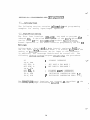
1.1 Product Description
The Z80-AIO is a 12-bit analog input/output card,
compatible with the Z80 Microcoinputer Board Series.
The analog to digital portion can accept 16 differential
or 32 single-ended channels with input voltages ranging
from (+/-) 2.5mV füll scale to (+/-) 10V füll scale.
The digital to analog portion provides two, 12-bit D/A
Converters with double buffering to minimize output
switching transients. The Output voltage is selectable
for bipolar or unipolar Operation with Output voltages
ranging from (+/-) 2.5V füll scale to (+/-) 10V füll
scale. This analog systera is interfaced äs I/O to the
CPU and may operate in a polling or interrupt mode. I/O
addressing may be changed by on-board jumper selections.
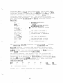
1.2
Block Diagram
CHAN STB
K
ADDR
\
/ DECODE
ADU
Rllfi
Y
STROBE
p>
3)
1
4
CONTROL r
\ INFS \
1
i
r^
ANALOG
MUX
•ANALOG
\ INPUTS
D
Z
N
INTR
ir
PIO
\
k/
DATA
BUS
INT
H
ir 1 1
^L
/l
<
^
CNTL &
TIMING
/
v,
SAMPLE & HOLD
AMPLIFIED
h^
INSTRU VIENTATION
AMPLIF ER
STB (A)^
12 BIT
A/D
CONV
^
— •
*f
12 BIT
D/A
CONV
N
ANALOG
OUTPUTS
STB (B)
L__^
Y
12 BIT
D/A
CONV
SECTION 2:
INSTALLATION
2.1 Introduction
The following section contains Information on initial
unpacking and inspection, power and Signal connections
to the MCB, and Installation of the AIO Board or AIB in
the MCZ l series Systems.
2.2 Initial Unpacking and Inspection
Inspect the product for shipping damage äs soon äs it is
unpacked. Check for any physical damage that may be
attributed to abuse and handling during shipment. If
the product is damaged in any way, notify the carrier
immediately.
2.3 Installation (MCZ-1)
The Analog Boards may be installed in either of the
prewired I/O board positions in the MCZ-1/20 or MCZ-1/25
Systems. These positions are J2 and J3 äs described in
the MCZ Hardware User's Manual. Jl, an undedicated and
unwired position, may also be used. In the MCZ-1/30
System, Jl, J2 and J3 of each card cage, may be used in
the identical manner äs previously described. In the
MCZ-1/05, -1/10 and PDS, Jl (User's Option) and J4
(Video Display Board) will directly accommodate the
Analog Boards.
2.4 Power and Signal Connections
The Z80 AIO and AIB are pin-compatible with the Z80 MCB
bus structure. For convenience, the wire list for
interconnection between the MCB and the Analog Boards is
provided:
TO
AIO:1-3, 59-51
AIO:4
AIO:5
Next IEI
AIO: 7
AIO: 8
AIO:12
AIO:13
AIO:23
AIO:26
AIO:29
AIO:30
AIO:62-64, 120-122
AIO:68
AIO:71
AIO:73
AIO:75
AIO:79
AIO:98
AIO:99
AIO:100
AIO:101
AIO:102
AIO:103
AIO:115
AIO:116
TABLE 2.3.1:
FROM
DESCRIPTION
MCB:l-3, 59-61
+5V P.S.
IORQDATA BIT (5)
IEO of AIO/AIB
IEI Of AIO/AIB
DATA BIT (3)
DATA BIT (6)
DATA BIT (0)
WRADDR. BIT (7)
ADDR. BIT (5)
ADDR. BIT (6)
COMMOM
DATA BIT (4)
DATA BIT (2)
DATA BIT (7)
DATA BIT (1)
INTADDR. BIT (4)
PHIADDR. BIT (3)
ADDR. BIT (2)
ADDR. BIT (1)
ADDR BIT (0)
MlRD-
MCB: 4
MCB: 5
AIO:6
Last used IEO
MCB: 8
MCB:12
MCB:13
MCB:23
MCB:26
MCB:29
MCB:30
MCB:62-64, 120-122
MCB:68
MCB:71
MCB:73
MCB:75
MCB:79
MCB:98
MCB:99
MCB:100
MCB:101
MCB:102
MCB:103
MCB:115
MCB:115
MCB TO AIO OR AIB WIRE LIST
SECTION 3:
OPERATION
3.1 Introduction
This section contains a qeneral description of the Analog
Boards 1 Operation, and provides some application Software for
initializing and communicating to the AIO and AIB.
3.2 Description
Interfacing the AIO or AIB to the System bus is accommodated
by the on-board PIO and is addressed äs I/O. The ADDRESS
DECODER uses ten addresses to direct all board operations.
By selecting the PIO port A or B control addresses, the PIO
may be prograinnied to Interrupt the CPU System and supply an
Interrupt vector address upon completion of an A/D
conversion. The CONTROL and TIMING will gate the requested
analog input channel to the ANALOG MULTIPLEXER, strobe the
SAMPLE and HOLD AMPLIFIER and request conversion of the A/D
CONVERTER. Upon completing the conversion, the A/D CONVERTER
will respond to the PIO through the CONTROL and TIMING that
the converted data is ready. At this time, the PIO may
Interrupt the System or the System may read the Status
register to find that the conversion data is ready and the
results have not previously been read.
Each 12-bit D/A converter has two I/O ports for the eight
least significant bits and the four most significant bits of
the data word. The 12-bit data word is formed and presented
to the DAC inputs for conversion when the most significant
byte is output.
3.3 Address Modifikation
The AIO or AIB Interfaces to the Z80 MCB I/O bus, occupying
ten locations in the I/O address space. The first four
locations are required for the PIO. The next two locations
are used to transfer the input channel address and board
Status while the remaining locations are used for passing
data to the two D/A Converters.
I/O ADDR.
FUNCTION
80
81
82
83
88
PORT A
PORT B
PORT A
PORT B
Address
89
8C
8D
8E
8F
Status Register
Low byte DAC l Register
High byte DAC l Register
Low byte DAC 2 Register
High byte DAC 2 Register
TABLE 3.3.1:
data
data
Control
Control
Register (Sei. Ch. No.)
PREWIRED I/O ADDRESSES
The board, äs received from the factory, is wired to occupy
those locations shown in Table 3.3.1. However, it is
possible to move the onboard PIO and the board registers
independently throughout the I/O address space. The only
limitations upon address selection are that the PIO and board
registers cannot occupy the same locations, and the three
most significant address bits must be the sänne.
Address modification is achieved by removing the existing
address selection Jumpers and then installinq those indicated
in Tables 3.3.2 and 3.3.3 for the desired address. Wherever
a "one" occurs in the address, the High jumper should be
installed. Wherever a "zero" occurs, the Low jumper should
be installed.
ADDRESS BIT
2
3
4
5
6
7
TABLE 3.3.2.
LOW
JP38
JP40
JP31
J^33
JP26
JP29
PIO Address Selection Jumpers.
ADDRESS BIT
3
4
5
6
7
TABLE 3.3.3.
HIGH
JP39
JP41
JP30
JP32
JP27
JP28
HIGH
JP37
JP34
JP32
JP27
JP28
LOW
JP36
JP35
JP33
JP26
JP29
Register Address Selection Jumpers
3.4 Input/Output Handling
Inputting of data can be accomplished in one of two modes;
Polling and Interrupt. These modes operate äs follows:
Polling Mode - During initialization of the PIO, the
Interrupt enable flag must be reset to prevent the generation
of Interrupts. When a conversion is desired, it is initiated
by writing the Analog Channel Address to the address
register. The program must then periodically test the
conversion bit in the Status register to determine v/hen the
conversion is complete.
Interrupt Mode - After setting the board's PIO Interrupt
enable and vector address, conversion is started by writing
to the address register. The program execution can then
continue until the end of conversion has occurred. At that
time, the PIO generates an Interrupt vector causing the CPU
to begin execution of the Interrupt Service routine.
Outputting Data - Outputting of data to the AIO's two D/A
Converters is straight-forward. The two 12-bit D/A
Converters have separate I/O addresses for the upper and
lower bytes of the data word. A word is formed by loading
the eight least significant bits into a latch where they are
buffered from the D/A inputs until the final four bits of the
data word are received. The combined 12-bits of data are
then gated simultaneously to the D/A inputs. This double
bufferinq scheme prevents conversion of partial words, and
therefore, eliminates spiking in the Output Signal.
3.5 Application
3.5.1 Input Range Selection
The data acquisition System has been jumpered for (+/-)10V
Operation. Other ranges are possible and can be selected äs
shown in Table 3.5.1.3.
RANGE
(+/-)10V
(+/-)5V
(+/-)2.5V
0 to +10V
0 to +5V
TABLE 3.5.1.1.
JUMPERS
W8*, W7*, W9*, W10*
W8*, JP21, W9*, W10*
W8*, JP20, JP21, W9*, WlO*
JP23, JP21, JP25, JP43
JP23, JP20, JP21, JP25, JP43
Input Range Setting Jumpers.
All jumpers marked with an asterisk (*) are installed at the
factory and are implemented by a plated-through hole
connecting pads on the upper and lower surfaces of the board.
These can be removed by careful manual drilling with a 0.055"
(#54) drill. All other jumpers are wire and should be
sleeved wherever a possible short could occur.
When the ränge is changed, those existing jumpers that are
not used for the new ränge must first be removed, and then
the Installation of the additional jumpers performed.
The analog to digital Converter Output data is normally
presented in 2"s complement format for bipolar ranges. For
straight binary Operation remove wire Jumper W9 and install
JP25.
3.5.2 Output Range Selection
Each DAC is jumpered at the factory for (+/-)10 volt
Operation and two's complement coding (Table 3.5.2.2).
However, it is possible to alter these jumpers äs shown in
Table 3.5.2.1 for other Output voltages. Jumpers indicated
by an asterisk are plated-through holes on the board and
should be removed by careful manual drilling with a 0.055"
(#54) drill. When making a change, first remove those
jumpers indicated for the present ränge, and replace them
with those jumpers recruired for the desired ränge.
JUMPERS
RANGE
(+/-)10V
(+/-)5V
(+/-)2.5V
0 to +10V
0 to +5V
TABLE 3.5.2.1.
DAC l
Wl*, W2*
JP11, W2*
JP11, W2*, JP9
JP11, JP8
JP11, JP8, JP9
DAC 2
W3*, W4*
JP15, W4*, JP13
JP15, JP12
JP15, JP12, JP13
Output Range Selection Jumpers.
When converting from bipolar to unipolar Operation, W5*
should be removed and JP7 installed. This converts from
two's complement Operation to straight binary.
Bipolar - Two's Complement
Digital Input/Output
0111...11 "(7FFH)
100...00 (800H)
(+/-)10V
+9.9951V
-10.0000V
(+/-)5V
+4.9975V
-5.0000V
(+/-)2.5V
+2.4988V
-2.5000V
^s.
Unipolar - Straight Binary
Digital Input/Output
111...111 (FFFH)
000...00 (OOOH)
TABLE 3.5.2.2.
0 to +10V
9.9975V
0.0000V
0 to +5V
4.9988
0.0000V
Analog Input and Output Füll Scale Range Values,
3.5.3 Differentlal-Single Ended Selected
The board, äs received from the factory, is wired for
differential input. The input System can be changed from
differential to single-ended or vice versa by simply changing
several jumpers. W6* is required for differential Operation,
and JP16 and JP18 are reauired for single-ended Operation.
W6* is a plated-through connection and should be removed by
careful manual drilling with a 0.055" (#54) drill.
Differential Operation is generally used to minimize common
mode noise during low level Operation. Single-ended
ooeration is suitable for large input Signals. However, a
noise reduction of ten-to-one can be achieved in single-ended
Operation by making a "pseudo differential" connection. This
involves sensing the ground at the signal source rather than
at the board. To use this method, all input Signals must be
on the sanie ground System at their source.
Pseudo-differential Operation occurs when jumper JP18 has
been removed and JPl is installed.
3.5.4 Input System Low Level Operation
When it is desired to operate the input systein
instrumentation amplifier at other than unity gain for low
level Signals, a simple change of the gain setting resistor
is all that is required. R8 and the optional parallel
resistor R9 form this resistance.
The value of the gain
setting resistor can be calculated from the following
formula:
20K
R =
G - l
Stable (10 ppm/deg C) wire-wound resistors should be used.
Increasing the amplifier gain also increases its settling
time. As a result, the System delay timer must be extended
by increasing the value of R15 and the optional parallel
resistor R14. Delays and values of R15 versus Gain are shown
in Table 3.5.4.1.
Amplifier Gain
l
10
100
1000
TABLE 3.5.4.1.
Delay Time (us)
20
30
40
100
R15 (+20%)
9.5K
14.3K
19K
47.5K
Delay Time vs. Amplifier Gain.
3.5.5 Input System Application
The data acquisition System, incorporated into the AIO or
AIB, uses a fixed timing sequence between channel selection
and the Start of data conversion. If desired, this time may
be increased by the addition of an external resistor and
capacitor. This procedure is described in the low level
Operation section.
Multiplexer
on Kt-sistdnct
FIGURE 3.5.5.1. On Channel Multiplexer Circuit for
Single-Ended Operation.
For a gain of l (set at factory), multiplexer settling time
is 20us which is sufficient for most application. The only
external factor which affects the multiplexer settling time
is the output impedance (Rs) of the source connected to a
channel. A circuit roodel of an "Cn" channel is shown in
Figure 3.5.5.1. The input capacitance (Cl) of 50pF for
single-ended Operation does not affect the settling time
since it is continuously connected to the source. The Signal
at the Output of the multiplexer must be allowed to settle to
(+/-)0.01% (nine time constants) to maintain the füll
accuracy of the System.
The multiplexer time constant can be
calculated with the formula: Ts = (Rs + Ron) Co. For a
source resistance of 1k, Ts = (l + 1.8k) x 50pF = 14 Ons.
Thus, 1.20us is needed to settle to +0.01%. This is well
below the fixed lOus allowed for multiplexer settling. The
accuracy of the System, is therefore, preserved.
If the source bandwidth can be limited, high impedance
sources may be accurately handled by placing a large
capacitor ecross the multiplexer input. An analysis of such
a circuit shows that a capacitor of O.SuF is sufficient. For
such a capacitance, the multiplexer time constant becomes
90ns. If this method cannot be used, the time allowed for
settling can be increased äs described in the section on low
level Operation.
10
For switchinq of large Signals, it must be remembered that
the on resistance is the channel resistance of a FET which IF
a nonlinear function of the applied voltaqes. As a result,
the previous calculations are only an approximation derived
from a linearized mode. Another factor not considered in the
above calculation is the addressing delay of the multiplexer.
This is typically 250ns and is additive to the above
calculated times.
For differential units, the same considerations apply. Even
though two input circuits are involved, there is sufficient
component matching within the multiplexer to prevent
measurable differences in the transfer functions for each
half of the Signal. When operated in the differential irode,
Co in Figure 3.5.5.1 becomes 12.5pF with an Ron = 1.8k in
each leg. Therefore, the time constant becomes one-half the
time constant for the single-ended channel.
The analog inputs have reversed-biased diode circuits which
prevent damage from discharge of static electricity.
However, it is still wise to take reasonable precautions
against static discharge.
3.5.6 Thermocouple Temperature Acauisition
Thermocouples are often used äs temperature sensors for
process control Systems. Thermocouples are characterized by
temperature coefficients of 10 to 70uV/deg C and operatinq
ranges of minus hundreds to plus thousands of degrees
centrigrade. When the AIO or AIB is operated with an
Instrumentation amplifier gain of 100 or more, it may be
connected directly to these devices. The wires running from
thermocouple measuring devices often pick up large
common-mode noise Signals of 60 Hz or higher freauencies.
The high common-mode rejection of the Instrument amplifier
will reject common-mode noise. To minimize differential mode
noise, the Signal wire should be twisted, and if possible,
shielded. As a rule, an unshielded twisted pair is better
than a coax but a shielded twisted pair is best.
The remote sensor should be earth-grounded to prevent
common-mode voltages from exceeding the +5 volt ränge of the
multiplexer. To complete a thermocouple System, it is
necessary to terminate all thermocouple wire pairs at an
isothermal box or connector strip of some type. An ordinary
11
barrier strip may be monitored to allow the observed
thermocouple cmf to be cold-junction compensated. Figure
3.5.6.2 shows a circuit for this purpose. The Output is
connected to one of the input channels to supply ambient
temperature data to the System Computer. Output sensitivity
is approximately 2 mV/deg C.
12
Cable Run
18k
CHN
IA
18k
^
J
47MF
r*\
Multiplexer
_/7h—
~^W~
—(7h—
~VÜ~
Thermocouple
CHN R 7 N
777Earth
Ground
^^-v^-\
Isothermal
Barner Strip
100N
lOHz Low
Pass Filter
FIGURE 3.5.6.1:
Thermocouple Input System
+ 15
20k
Rd
Rc+Rd 0
I / 1 0 ( R ü l! Rh)
430n
+
Ra
kT
R i 7 > -TT l n
Rd
~ ~ Rc + Rd ('
+
Ra _K
Rh ) it; '"
T = °K, k/q = 8.67 x 10 -S
Dual monohthii transistor pair (National LM l 14)
Mounted Near Isothermal
Barner Strip
FIGURE 3.5.6.2:
Ambient Temperature Sensor
13
10
10
100M
SECTION 4:
4.1
PROGRAMMING AND INITIALISATION
Introduction
The following section contains Information and programming
examples for analog input/output Operation.
4.2 Input Programming
The first four locations (80H-83H), are used to program the
onboard PIO. A detailed description of the PIO's Operation
can be found in the Zilog Z80-PIO Product Specification.
Normal Operation of the board reauires programming the PIO äs
follows:
Polling Mode - Both A and B Mode Control registers must be
set for input (mode 1) . When Mode l is active, data from the
analog to digital Converter can be input to the processor.
In addition, the Interrupt Enable must be turned off. The
following initialization program illustrates the procedure.
DI
;
DISABLE INTERRUPT
;
;
SET PORT A FOR MODE l
SET PORT B FOR MODE l
;
;
;
;
DISABLE PORT A INTERRUPT
DISABLE PORT B INTERRUPT
INITIALIZE CONVERSION READ F.F,
INITIALIZE CONVERSION READ F.F,
LD A, 4FH
OUT 82H, A
OUT 83H, A
LD A, 07H
OUT 82H, A
OUT 83H, A
IN A, 80H
IN A, 81H
The remaining board locations are treated äs described in the
following paragraph discussing non-PIO locations.
14
Interrupt Mode - As in the Polling Mode, the A and B Mode
Control Registers must be set for Input (Mode 1). The PIO
Interrupt System is enabled by loading the interrupt vector
address and setting the interrupt enable. Only Port 3
interrupt enable should be set. The following program
illustrates the procedure.
In addition to initializing the
PIO, the program also loads the ZSO's Interrupt Vector
Register.
DI
LD A, N
;
LD I , A
;
LD A, M
OUT 83H, A
LD A, 4FH
OUT 82H, A
OUT 83H, A
LD A, 07H
OUT 82H, A
LD A, 87H
OUT 83H, A
IN A, 80H
IN A, 81H
IM 2
EI
;
DISABLE INTERRUPT
(LOAD I VECTOR REGISTER
WITH NUMBER ( N ) )
SET PIO INTERRUPT VECTOR
SET PORT A FOR MODE l
SET PORT B FOR MODE l
DISABLE PORT A INTERRUPT
SET PORT B INTERRUPT
INITIALIZE PORT A DATA
INITIALIZE PORT B DATA
SET INTERRUPT MODE 2
The remaining non-PIO locations are programmed äs follows:
Non-PIO Location - Location 88H specifies the particular
analog input channel to be digitized. Writing the channel
number (0-20H) into the Address Register at this location
will cause a conversion to be performed.
The Status Register (See Figure 4.3.1) at location 89H
provides data on A/D Performance. Bit 0 indicates that a
conversion is in progress by displaying a 0 during this tiirte
and a l at all other times. Bit l is 0 after a conversion
has been performed and then chanqes to l after the first
complete reading of the converted data.
B7
X
(X:
B6
X
B5
X
B4
X
B3
X
B2
X
indicates unused)
FIGURE 4.3.1
STATUS REGISTER BIT LOCATIONS
15
Bl
READ
STATUS
BÖ
A/D
STATUS
4.3
Output Programming
As shown in Table 3.3.1, the two digital to analog Converters
occupy locations 8CH - 8FH. Either Converter is programmed
by loading the least significant eight bits of data into its
Low Byte location. The most significant four bits of data
are then loaded into the right most bit locations of the
Converter's high data byte. The most significant four bits
of this byte are unused. Figure 4.3.2 illustrates this bit
placement.
DB7
LOW BYTE PORT ADDRESS
DB6
DBS
DB4
X
HIGH BYTE PORT ADDRESS (8DH OR 8FH)
X
X
X
DBll
DB10
FIGURE 4.3.2.
(8CH OR SEH)
DB3
DB2
DAC BIT PLACEMENT
16
DBl
DB9
DBO
SECTION 5:
TESTING
5.1 Introduction
The following section contains Information on suggested test
equipment and test aids, calibration procedure, and a
description of the available calibration and test routines
for the AIO and AIB on the MCZ-1.
5.2 Test Equipment and Aids
Calibration is performed by connecting a precision voltage
source capable of 0.005% accuracy or by using a DC voltage
source of less absolute accuracy, the Output of which is
monitored by a five digit DVM capable of (+/-) 0.005%
accuracy. To utilize the MCB-1 system-based loop test
described in section 5.4, test routines 15 and 16, a test
plug is used to Jumper the analog Output of DAC l to the
single- ended analog inputs of channeis 0-15 and the analog
Output DAC 2 to the single-ended analog inputs channeis
16-31. The wire list for connecting the back panel connectors
2 and 3 to accommodate this test arrangement is äs follows:
TO
J2:6-9, 18-21
J3:l-4, 14-17
J2:10-13, 22-25
J3:5-8, 18-21
TABLE 5.2.1:
FROM
J2:3
J2:3
J2:15
J2:15
DESCRIPTION
DAC 1-OUT TO
DAC 1-OUT TO
DAC 2-OUT TO
DAC 2-OUT TO
Test Plug Wire List
17
CH
CH
CH
CH
0-7
8-15
16-23
24-31
5.3 Calibration
Input System Calibration
System Calibration is typically performed on a single channel
while running the following program. The program assumes
that the Polling Mode initialization has been
performed äs described in the Programming section.
AD:
AE:
AC:
AA:
AB:
AF:
LD BC, OH
LD D, 64H
LD A, 0
OUT 88H, A
IN A, 89H
AND 01H
JP NZ, AC
IN A, 80H
LD L, A
IN A, 81H
LD A, L
SUB REF
;LOAD ADDP. REG WITH CH. #
;IS CONVERSION COMPLETE?
;NO.
;YES. READ DATA
;IS DATA = LOW REF.?
;REF = OH FOR OFFSET ADJ.
REF = FFH FOR GIAN ADJ.
JP Z, AA
INC C
JP AB
INC B
DEC D
;NO. INCREMENT COUNT
;YES. INCREMENT COUNT
;HAVE 100 CONVERSIONS BEEN
;PERFORMED?
JP NZ, AE
JP AD
END
;YES. REPEAT
The program has been written to accommodate factory
preset addresses. If the board responds to other
addresses, the program references to I/O locations
must be made to conform with these new locations.
After assembling and loading, insert a breakpoint
at location AF. The offset and gain adjustments
on the System are made while applying the voltages
shown in Table 5.3.1. The offset voltage
adjustment is made at the most negative value of
the ränge, less 1/2 least significant bit
(LSB). An LSB is egual to the span (füll scale
ränge) divided by 4096 for 12-bit resolution. The
gain adjustment is made at the most positive ränge,
less 3/2 LSB. Thus, for a ränge of (+/-) 10V
18
an LSB is 20V/4096 = 4.88mV. The offset
adjustment is made at -10V + 2.44mV = -9.9976V
and the gain adjustment at +10V -7.32mV = +9.9926V.
Before making these adjustments, however, the unit
should be allowed to reach thermal eguilibrium (about
30 minutes under power).
The offset adjustment is made first. The calibration
program is then run, and after 100 conversions, it will
halt at the break point. The contents of B and C registers
should be compared. The contents of Register B is the number
of times the conversion results exactly matched the reference
value. The contents of Register C is the number of times the
conversion results did not match the reference value.
Ideally, Register B should have a value of 64H and Register C
should have a value of 0. However B = 50 and C = 50
indicates an acceptable offset or gain adjustment setting.
The gain adjustment is roade in much the same manner.
However, the value of REF is changed from 0 to FF.
The appropriate gain voltage is then applied, and the
calibration procedure performed äs described for the
offset adjustment.
Range
(+/-UOV
(+/-)5V
(+/-)2.5V
0 to +10
0 to +5
TABLE 5.3.1:
Note:
RV5:
RV6:
Offset
-9.9976V
-4.9988V
-2.4994V
+1.22mV
+0.61mV
Gain
+9.9926V
+4.9963V
+2.4981V
+9.9953V
+4.9981V
Data Acquisition Calibration Values
ADC gain adjustment
ADC offset adjustment
19
Output System Calibration
The Output System is calibrated through the use of the
following program.
START:
LD A, LSB
;LSB = OH FOR OFFSET ADJ.
LSB = FFH FOR GAIN ADJ.
OUT (DACL),A
;OUTPUT LSB TO DAC LOW BYTE REG.
;MSB = OF8H FOR BIPOLAR OFFSET
MSB = OH FOR UNIPOLAR OFFSET
MSB = 7H FOR BIPOLAR GAIN
MSB = OFH FOR UNIPOLAR GAIN
LD A, MSB
OUT (DACH), A
JP START
DACL EQU XX
;OUTPUT MSB TO HIGH BYTE REG.
;XX IS THE I/O ADDR OF DACL I.E. 8CH
;OR SEH
DACH EQU XX
;XX IS THE I/O ADDR OF DACH I.E. 8DH
;OR 8FH
END
Before tbe program is assembled, DACL and DACH must be set to
the I/O addresses of the low and high bytes of the digital to
analog Converter to be calibrated.
After assembling and loading, a breakpoint should be set at
the Jump instruction. When the program has been run, the
desired Converter will be set at its most negative Output.
The DAC should then be set by its offset control for its most
negative füll scale Output value, äs shown in Table 5.3.2.
However, before making this adjustment, the board should be
allowed to reach thermal eguilibrium -- about 30 minutes
under power.
20
After the Offset adjustment has been made, the appropriate
values of LSB and MSB for Gain adjustment must be deposited
into the program. The previous procedure must then be
repeated, but adjust the gain control for the most positive
füll scale Output value.
Range
Low
High
l LSB
(+/-)10V
(+/-)5V
(+/-02.5V
0 to +10V
0 to +5V
-10.000V
-5.000V
-2.500V
0.0V
0.0V
+9.9951V
+4.9976V
+2.4987V
+9.9975V
+4.9988V
4.8848mV
2.4414mV
1.2207mV
2.4414mV
1.2207mV
TABLE 5.3.2:
DAC Calibration Values
Note:
DAC1
DAC2
DAC2
DAC1
RV1:
RV2:
RV3:
RV4:
gain adjustment
gain adjustment
offset adjustment
offset adjustment
21
5.4 System Test
The following tests are provided with the Analog Board and
are applicable to the operating Systems available in the
MCZ-1 Series Systems. The test's titles and descriptions are
given in the table below.
Test l - DAG l Bilpolar Offset
Description
When the program has been run, DAC l will be set at its most
negative Output. The DAC should then be set by its offset
control for its most negative füll scale Output value äs
indicated in Table 5.3.2. RV4 is the offset adjustment
control for DAC 1.
Test 2 - DAC l Bipolar Gain
Description
When the program has been run, DAC l will be set at its most
positive output value. The DAC should then be set to its
most positive füll scale Output value for the selected ränge,
äs indicated in Table 5.3.2. The gain control for DAC l is
RV1.
Test 3 - DAC l Unipolar Offset
Description
This test is performed in the same manner äs Test 1.
Test 4 - DAC l Unipolar Gain
Description
This test is performed in the same manner äs Test 2.
22
Test 5 - DAC 2 Bipolar Offset
Description
This test is performed in the same manner äs Test 1.
offset adjustment control for DAC 2 is RV3.
The
Test 6 - DAC 2 Bipolar Gain
Description
This test is performed in the same manner äs Test 2.
gain control for DAC 2 is RV2.
The
Test 7 - DAC 2 Unipolar Offset
Description
This test is performed in the same manner äs Test 5.
Test 8 - DAC 2 Unipolar Gain
Description
This test is performed in the same manner äs Test 6.
Note: Before making any of these adjustments, the board
should be allowed to reach thermal equilibrium, about 30
minutes under power. Additionally, the gain and offset
controls may contain some lash-back and should be alternately
rechecked after initial adjustment.
23
Test 9 - Data Acauisition - Bipolar Offset
Description
The offset adjustment is made at the most negative value of
the selected ränge less one-half the least significant bit.
The values are shown for the selected ränge in the Data
Acguisition Calibration Table 5.3.1. The test will check the
actual conversion value against the expected conversion value
and respond with the message "Turn Control Clockwise", or
"Turn Control Counter Clockwise". When the actual value is
within (+/-)20H of the expected value for 100 consective
conversions, the program will exit with the message message
"Control set Correctly" and "Test ?". The offset adjustment
control is RV 6.
Test 10 - Data Acauisition - Bipolar Gain
Description
The gain adjustment is made in much the same manner äs the
offset adjustment.
The appropriate gain value from the Data
Acauisition Table for the selected ränge is applied in the
calibration procedures performed äs described for the offset
adjustment. The gain adjustment control is RV5.
Test 11 - Data Aquisition - Unipolar Offset
Descr iption
This test is performed in a similar manner to Test 9 using
the appropriate values from the Table 5.3.1.
Test 12 - Data Acauisition - Unipolar Gain
Description
This test is performed in a similar m.anner to Test 10 using
the appropriate values from the Table 5.3.1.
24
Test 13 - Generate Ramp DAC l
Description
This test generates a ramp from a chronological sequence
exercising the DAC to its minimum and maximum values of the
conversion ränge. The test is intended for observation only
and does not imply that monotinicity and linearity can be
measured or accurately observed with Standard laboratory
equipment.
Test 14 - Generate Ramp DAC 2
Description
This test is the same äs Test 13 and applies to DAC 2.
Test 15 - Bipolar Continuity Test - Pulling Mode
Descr iption
This test checks for missing codes by feeding the analog
Output into the analog input and comparing the conversion
results of the A/D Converter to the data word of the D/A
converter. If the actual conversion word is within (+/-)!
LSB of the expected conversion word, then the test will
increment to the next chronological D/A word and perform the
test again. This process is continuecl until the entire ränge
of conversion is tested for that analog input channel. The
analog input channel is then incremented, and the input ränge
is again tested in its entirety. This process is repeated
until all analog input channels have been tested. During the
couse of the test, if a channel fails to match the expected
data word within +1 LSB, the test will respond with the
message "Channel A failure data is BCDE should be FGHI",
where channel A may ränge from 0-31 and BCDE and FGHI are
actual and expected data words. "Do you want test repeated?"
A response of "yes" will repeat the test for the same channel
and data word. A response of "no" will increment the data
word to the next chronological number. After all channels
have been exercised, the test will respond with the message
"End of test" and "Test number ?" The test fixture to juroper
the analog input to the analog Output has been previousiy
described. This test operates by checking the Status word or
conversion complete. This is known äs Polling Mode.
25
Test 16 - Bipolar Continuity Test - Interrupt Mode
Description
This test operates in the same manner äs Test 15, except that
the program does not check the Status word but is interrupt
driven.
Note: To use Test 16, the interrupt enable input to the
analog board raust be connected to the previous device in
interrupt daisy chain.
26
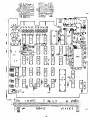
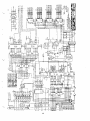
SECTION 6:
6.1
TECHNICAL DESCRIPTION
Introduction
The following section contains a detailed description of the
Operation and logical throughput of the AIO. The reader is
directed to use the accompanying schematic at the end of the
manual äs a reference. The AIB, being a subset of the AIO,
is not noticeably discriminated in the description. All
references to analog input are applicable to both boards.
The boards 1 specification is also included in this section.
6.2
Description
The AIO
address
decodes
through
is programmed äs I/O ports. IC20 and IC26 decode
bus lines AB3-AB7 to select the board itself. IC21
address bus lines ABO, ABI, and AB2. Jumpers JP29
JP40 determine the address of the board.
Conversion of an input channel is started by writing the
channel number to the board (location 88H). When address
lines AB2, ABI, and ABO are logic 0 and WR- is active, Pin l
of IC22 will go high latching the input channel number into
IC23. The same signal also triggers the first one-shot in
ICH. This one-shot times out 20 microseconds to allow for
settling of the input multiplexers, instrumentation
amplifier, and sample-hold amplifier. At the end of this
time, it turns the sample-hold amplifier to Hold by
outputting a pulse from Pin 13, ICH, to Pin 8 of IC12. This
same pulse also triggers the second one-shot in ICH at Pin
9. The Output of the second one-shot, Pin 5 of ICH, is
connected to Pin 18 of SMS which immediately Starts
conversion in the A/D Converter. The Output of the first
one-shot, Pin 13, of ICH, and Pin 22 of SM3 go through an
"OR" gate of IC28. The Output of the "OR" gate connects to
the data bus (DO) at Pin 13 of IC27 to provide Status
Information. DO is low during the conversion process. DO is
high when conversion is complete and data is ready at the
Output of the A/D Converter. Data is Output from the A/D
Converter, SM3, on Pins 1-6 and 27-32. The Outputs are then
connected through IC33 and IC34 to the PIO, IC32, Pins 7-15
and 27-30. When the AIO is read, address lines AB2 and ABI
are egual to logic 0. The eight least significant bits of
data are Output when ABO is logic 0 and the four most
significant bits are Output when ABO is logic 1. ABO is
connected to the PIO from IC27, Pin 3, to IC32, Pin 6.
27
The analog input Signals are connected at connectors P2 and
P3 through input protection resistors R27-R58 to the input
CMOS itiultiplexers, IC3, 4, 5, and 6. The input multiplexers
are shipped connected äs 16 channel differential. The
Instrumentation amplifier, which consists of amplifiers AI,
A2, and A3, is connected in the differential mode. The
resistance inserted at R8, in parallel with R9, determines
the gain of the instrumentation amplifier.
Data is transferred to the Output D/A Converters, SMl and SM2
by writing to the board. Address line, ABI, controls to
which DAC data is written. With ABO a logic 0, the eight
least significant bits are written to the board and stored in
IC8 and IC16. With ABO a logic l, the four roost significant
bits are written to the board and buffered by IC25.
When ABO is a logic l and WR- is active, data is written to
the D/A Converter that is selected by ABI. When ABI is a
logic 0, data is written to IC9 and IC17 which störe data for
SMl. When ABI is a logic l, data is transferred to IC10 and
IC18, which Stores data for SM2.
28
6.3
Specification
Typical at 25deg C and rated power supplies unless otherwise
noted.
ANALOG INPUT SECTION (AIO/AIB)
Input characteristics
Number of Channels
ADC Gain Ranges (Jumper Selectable)
Amplifier Gain Ranges (Resistor Prog.)
Maximuin Input Voltage Without Damage
Input Impedance
Bias Current
Differential Bias Current
32 single-ended/16 diff
0-5V, 0-10V, (+/-) 2.5V,
(+/-) 5V, (+/-) 10V
l to 1000
+26 volts
lOOMohm , 10 pF OFF Channel
lOOMohm , 100 pF ON Channel
20 nA
10 nA
Transfer Characteristics
Resolution
Throughput Time (max.) G = l
12 bits
45 usec/channel
Accuracy
System Accuracy st +25deg C (max.), Note l
Linear ity
Differential Linearity
Quantizing Error
Monotonicity, Note 3
+0.25% FSR, Note 2
+1/2 LSB
+1/2 LSB
+1/2 LSB
Guaranteed Odeg C to +70deg C
Stability Over Temperature, Note 4
System Accuracy Drift (max.) G=l
(+/-) 30 ppm of FSR/deg C
Dynamic Accuracy
Sample and Hold Aperature Time
Aperature Time Uncertainity
Differential Amplifier CMR
Channel Crosstalk
30 ns
(+/-)5 ns
74 dB (DC to IkHz)
80 dB down at IkHz, for
OFF channel to On channel
ANALOG OUTPUT SECTION (AIO)
Output Characteristics
Number of Channels
Output Voltage Ranges (Strap Selectable)
29
2
0 to +5V, 0 to +10V
(+/-)2.5V, (+/D5V,
(+/-)10V at 5mA Output Output
l ohm
Tmpedance
Transfer Characteristics
Resolution
Output Settling Time (max.)
12 bits
10 usec
Accuracy
Output Accuracy
Temperature Coeffient of Accuracy
FSR
+30 ppm of FSR/deg C
MECHANICAL
Environmental
Operating Temperature
Storage Temperature
Relative Humidity
Odeg C to +70deg C
-25deg C to +85deg C
95% noncondensing
Mechanical
Length
Depth
Thickness
Maximum Component Height
7.7 in/19.6 cm
7.5 in/19.1 cm
.062 in/0.16 cm
.4 in/1.02 cm
ELECTRICAL
+5V (+/-)5% at 1.6A
Power Converter Requirements:
Available to User*
DC Output
+ 15V
-15V
AIO
Oma*
15ma*
AIB
50ma*
65ma*
70 deg C
25 deg C
Oma*
15ma*
50ma*
65ma*
70 deg C
25 deg C
30
Connectors
VENDOR
PART NO.
DESCRIPTIQN
Garry Mfg. Co.
4000-2
Augat
14005-19P1
Ansley
Ansley
Ansley
609-2615M
171-26
609-255
122-pin edge
(100 mil spacing)
122-pin edge
(100 mil spacing)
Analog edge
Gable
Analog socket
NOTES
1. Includes offset errors, gain errors, linearity errors at
gain = 1.
2. FSR mean Füll Scale Range.
3. No missing codes guaranteed.
4. Includes offset drift, gain drift, and linearity drift.
31
SECTION 7:
MAINTENANCE
7.1 Introduction
This section contains Information on maintenance of the
analog boards.
7.2 Drift
In any System, powered on Operation will cause the components
to drift from their original values. This is particularly
evident in analog Systems. The Eurr-Brown components, used
on the AIO and AIB, use thin-film laser-trimmed resisters
with a typical absolute temperature coefficient of 20-60
parts per million and a ratio temperature coefficient of 3-5
parts per million.
Conseouently, in one year, the typical
drift could be 200-600 parts per million and the typical
ratio drift could be 25-50 parts per million. This means
that after 400 hours of Operation, the offset could have
drifted 1LSB, and that after 43000 hours of Operation, the
conversion may no longer be monotonic or linear. The offset
and gain ad^ustments should be checked once every six months.
32
SECTION 8:
DRAWINGS
8.1 Introduction
This section contains the scheraatic pinout lists and the
asseinbly drawing for the AIO and AIO.
33
J Jjj** * * *-*.,
|;3jji33i" u
1 « f ?f « ^ » »
n, A m ~w
IM Hf
QBLIZtt
\
m n m m ^-A l
'
1l ' H*i
t.f s! *
U
l l l
l
C17
l
i IM» i.
/ff
*<* ,
*^^
34
o
1 ) 1
**
-'
.,.«.
35
AIO I/O CABLES P2 AND P3
WIRB
1
2
3
4
5
6
7
8
9
10
11
12
13
14
15
16
17
18
19
20
21
22
23
24
25
26
AIO EDGE
CONNECTOR
1
2
3
4
5
6
7
8
9
10
11
12
13
14
15
16
17
18
19
20
21
22
23
24
25
26
ANSLEY "D"
CONNECTOR
—
13
25
12
24
11
23
10
22
9
21
8
20
7
19
6
18
5
17
4
16
3
15
2
14
1
P2 SIGNALS
CH23 (RT7)
CH23 (RT7)
CH22 (RT6)
CH21 (RT5)
CH20 (RT4)
CH19 (RT3)
CH18 (RT2)
CH17 (RT1)
CH16 (RTO)
CH7
CH6
CHS
CH4
CH3
CH2
CH1
CHO
SM1-GND
SM1-FB
ANALOG COMMON
SM2-GND
SM1-OUT
SM2-OUT
SM2-FB
-15V
+15V
36
P3 SIGNALS
REMOTE COMMON
REMOTE COMMON
-15V
+ 15V
ANALOG COMMON
ANALOG COMMON
ANALOG COMMON
ANALOG COMMON
ANALOG COMMON
ANALOG COMMON
CH30 (RT14)
CH31 (RT15)
CH28 (RT12)
CH29 (RT13)
CH26 (RT10)
CH27 (RTll)
CH24 (RT8)
CH25 (RT9)
CH14
CH15
CH12
CH13
CH10
CH11
CHS
CH9
PINOUT FOR AIO BOARD
PIN #
001
002
003
004
005
006
007
008
009
010
011
012
013
014
015
016
017
018
019
020
021
022
023
024
025
026
027
028
029
030
031
032
033
034
035
036
037
038
039
040
041
042
043
044
SIGNAL NAME
(+5V.PRINTED.DISTRIBUTION)
(+5V.PRINTED.DISTRIBUTION)
(+5V.PRINTED.DISTRIBUTION
IORODBS
IEO
IEI
DB3
DBG
DBO
WRAB7
AB5
AB6
TP3
TP13
TP12
37
045
046
047
048
049
050
051
052
053
054
055
056
057
058
059
060
061
062
063
064
065
066
067
068
069
070
071
072
073
074
075
076
077
078
079
080
081
082
083
084
085
086
087
088
089
090
091
092
TP11
TP10
TP9
TP8
TP7
TP6
TP5
TP4
TP1
(+5V.PRINTED.DISTRIBUTION)
(+5V.PRINTED.DISTRIBUTION)
(+5V.PRINTED.DISTRIBUTION)
(GND.PRINTED.DISTRIBUTION)
(GND.PRINTED.DISTRIBUTION)
(GND.PRINTED.DISTRIBUTION)
DB4
TP18
DB2
DB7
DB1
TP17
TP16
INT-
38
093
094
095
096
097
098
099
100
101
102
103
104
105
106
107
108
109
110
111
112
113
114
115
116
117
118
119
120
121
122
TP15
TP14
AB4
PHIAB3
AB2
ABI
ABO
MlRDTP2
(GND.PRINTED.DISTRIBUTION)
(GND.PRINTED.DISTRIBUTION)
(GND.PRINTED.DISTRIBUTION)
39
SECTION 9:
SUPPLEMFNTARY INTROOUCTICN
9.1 Introduction
The following section contains iistinqs and references to
additional sources of Information that may be of assistance
in implementing the user's application, and aid in better
understanding the Operation of the analog board in a
microcomputer-based System.
9.2 Li?t of Supplementary Information
Burr-Brown Application Note AN-79
Burr-Brown Product Specification ADC 80
Burr-Brown Product Specification DAC 80
Zilog PIO Product Specification
Zilog PIO Technical Manual
Zilog Interrupt Structure Application Note
40