1
Introduction to the Altera SOPC Builder
Using VHDL Design
This tutorial presents an introduction to Altera’s SOPC Builder software, which is used to implement a system
that uses the Nios II processor on an Altera FPGA device. The system development flow is illustrated by giving
R
step-by-step instructions for using the SOPC Builder in conjuction with the Quartus
II software to implement a
simple system.
The last step in the development process involves configuring the designed circuit in an actual FPGA device,
and running an application program. To show how this is done, it is assumed that the user has access to the Altera
R
II software
DE2 Development and Education board connected to a computer that has Quartus II and Nios
installed.
The screen captures in the tutorial were obtained using the Quartus II version 7.1; if other versions of the
software are used, some of the images may be slightly different.
Contents:
Nios II System
Altera’s SOPC Builder
Integration of the Nios II System into a Quartus II Project
Running the Application Program
1
Altera’s Nios II is a soft processor, defined in a hardware description language, which can be implemented
R
in Altera’s FPGA devices by using the Quartus
II CAD system. To implement a useful system it is necessary
to add other funcional units such as memories, input/output interfaces, timers, and communications interfaces.
To facilitate the implementation of such systems, it is useful to have computer-aided-design (CAD) software for
implementing a system-on-a-programmable-chip (SOPC). Altera’s SOPC Builder is the software needed for this
task.
This tutorial provides a basic introduction to Altera’s SOPC Builder, which will allow the reader to quickly
implement a simple Nios II system on the Altera DE2 board. For a fuller treatment of the SOPC Builder, the
reader can consult the Nios II Hardware Development Tutorial. A complete description of the SOPC Builder can
be found in the Quartus II Handbook Volume 4: SOPC Builder. These documents are available on the Altera web
site.
1 Nios II System
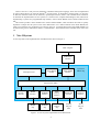
A Nios II system can be implemented on the DE2 board as shown in Figure 1.
Host computer
USB-Blaster
interface
Nios II processor
JTAG Debug
module
JTAG UART
interface
Cyclone II
FPGA chip
Avalon switch fabric
On-chip
memory
SRAM
interface
SDRAM
interface
Flash
memory
interface
Parallel I/O
interface
Serial I/O
interface
SRAM
chip
SDRAM
chip
Flash
memory
chip
Parallel
I/O port
lines
Serial
I/O port
lines
Figure 1. A Nios II system implemented on the DE2 board.
2
The Nios II processor and the interfaces needed to connect to other chips on the DE2 board are implemented
in the Cyclone II FPGA chip. These components are interconnected by means of the interconnection network
called the Avalon Switch Fabric. The memory blocks in the Cyclone II device can be used to provide an on-chip
memory for the Nios II processor. The SRAM, SDRAM and Flash memory chips on the DE2 board are accessed
through the appropriate interfaces. Parallel and serial input/output interfaces provide typical I/O ports used in
computer systems. A special JTAG UART interface is used to connect to the circuitry that provides a Universal
Serial Bus (USB) link to the host computer to which the DE2 board is connected. This circuitry and the associated
software is called the USB-Blaster. Another module, called the JTAG Debug module, is provided to allow the host
computer to control the Nios II system. It makes it possible to perform operations such as downloading programs
into memory, starting and stopping execution, setting breakpoints, and collecting real-time execution trace data.
Since all parts of the Nios II system implemented on the FPGA chip are defined by using a hardware description language, a knowledgeable user could write such code to implement any part of the system. This would be
an onnerous and time consuming task. Instead, one can use the SOPC Builder to implement a desired system
simply by choosing the required components and specifying the parameters needed to make each component fit
the overall requirements of the system. In this tutorial, we will illustrate the capability of the SOPC Builder by
designing a very simple system. The same approach is used to design large systems.
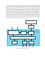
Host computer
Reset_n
USB-Blaster
interface
Clock
Nios II processor
JTAG Debug
module
JTAG UART
interface
Avalon switch fabric
On-chip
memory
Switches
parallel input
interface
SW7
SW0
LEDs
parallel output
interface
LEDG7
Figure 2. A simple example of a Nios II system.
3
LEDG0
Cyclone II
FPGA chip
Our example system is given in Figure 2. The system realizes a trivial task. Eight toggle switches on the DE2
board, SW 7 − 0, are used to turn on or off the eight green LEDs, LEDG7 − 0. The switches are connected to the
Nios II system by means of a parallel I/O interface configured to act as an input port. The LEDs are driven by the
signals from another parallel I/O interface configured to act as an output port. To achieve the desired operation, the
eight-bit pattern corresponding to the state of the switches has to be sent to the output port to activate the LEDs.
This will be done by having the Nios II processor execute a program stored in the on-chip memory. Continuous
operation is required, such that as the switches are toggled the lights change accordingly.
We will use the SOPC Builder to design the hardware depicted in Figure 2. Next, we will assign the Cyclone II
pins to realize the connections between the parallel interfaces and the switches and LEDs which act as I/O devices.
Then, we will configure the FPGA to implement the designed system. Finally, we will use the software tool called
the Nios II Debug Client to assemble, download and execute a Nios II program that performs the desired task.
Doing this tutorial, the reader will learn about:
• Using the SOPC Builder to design a Nios II-based system
• Integrating the designed Nios II system into a Quartus II project
• Implementing the designed system on the DE2 board
• Running an application program on the Nios II processor
2 Altera’s SOPC Builder
The SOPC Builder is a tool used in conjuction with the Quartus II CAD software. It allows the user to easily
create a system based on the Nios II processor, by simply selecting the desired functional units and specifying
their parameters. To implement the system in Figure 2, we have to instantiate the following functional units:
• Nios II processor, which is referred to as a Central Processing Unit (CPU)
• On-chip memory, which consists of the memory blocks in the Cyclone II chip; we will specify a 4-Kbyte
memory arranged in 32-bit words
• Two parallel I/O interfaces
• JTAG UART interface for communication with the host computer
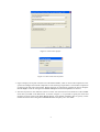
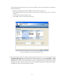
To define the desired system, start the Quartus II software and perform the following steps:
1. Create a new Quartus II project for your system. As shown in Figure 3, we stored our project in a directory
called sopc_builder_tutorial, and we assigned the name lights to both the project and its top-level design
entity. You can choose a different directory or project name, but be aware that the SOPC Builder software
does not permit the use of spaces in file names. For example, an attempt to use a directory name sopc
builder tutorial would lead to an error. In your project, choose the EP2C35F672C6 chip as the target device,
because this is the FPGA on the DE2 board.
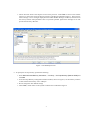
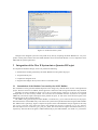
2. Select Tools > SOPC Builder, which leads to the pop-up box in Figure 4. Enter nios_system as the system
name; this will be the name of the system that the SOPC Builder will generate. Choose VHDL as the target
HDL, in which the system module will be specified. Click OK to reach the window in Figure 5.
4
Figure 3. Create a new project.
Figure 4. Create a new Nios II system.
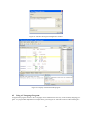
3. Figure 5 displays the System Contents tab of the SOPC Builder, which is used to add components to the
system and configure the selected components to meet the design requirements. The available components
are listed on the left side of the window. Before choosing our components, examine the area in the figure
labeled Target. Check the setting for the Device Family and ensure that Cyclone II is selected.
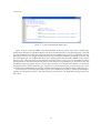
4. The Nios II processor runs under the control of a clock. For this tutorial we will make use of the 50-MHz
clock that is provided on the DE2 board. As shown in Figure 5, it is possible to specify the names and
frequency of clock signals in the SOPC Builder display. If not already included in this list, specify a clock
named clk with the source designated as External and the frequency set to 50.0 MHz.
5
Figure 5. The System Contents tab window.
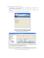
5. Next, specify the processor as follows:
• On the left side of the window in Figure 5 select Nios II Processor and click Add, which leads to the
window in Figure 6.
Figure 6. Create a Nios II processor.
6
• Choose Nios II/e which is the simplest version of the processor. Click Finish to return to the window
in Figure 5, which now shows the Nios II processor specified as indicated in Figure 7. There may be
some warnings or error messages displayed in the SOPC Builder Messages window (at the bottom of
the screen), because some parameters have not yet been specified. Ignore these messages as we will
provide the necessary data later.
Figure 7. The defined processor.
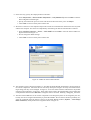
6. To specify the on-chip memory perform the following:
• Select Memories and Memory Controllers > On-Chip > On-Chip Memory (RAM or ROM) and
click Add
• In the On-Chip Memory Configuration Wizard window, shown in Figure 8, set the memory width to
32 bits and the total memory size to 4 Kbytes
• Do not change the other default settings
• Click Finish, which returns to the System Contents tab as indicated in Figure 9
7
Figure 8. Define the on-chip memory.
Figure 9. The on-chip memory is included.
8
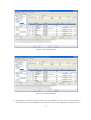
7. Specify the input parallel I/O interface as follows:
• Select Peripherals > Microcontroller Peripherals > PIO (Parallel I/O) and click Add to reach the
PIO Configuration Wizard in Figure 10
• Specify the width of the port to be 8 bits and choose the direction of the port to be Input, as shown in
the figure
• Click Finish to return to the System Contents tab as given in Figure 11
Figure 10. Define a parallel input interface.
Figure 11. The parallel input interface is included.
9
8. In the same way, specify the output parallel I/O interface:
• Select Peripherals > Microcontroller Peripherals > PIO (Parallel I/O) and click Add to reach the
PIO Configuration Wizard again
• Specify the width of the port to be 8 bits and choose the direction of the port to be Output
• Click Finish to return to the System Contents tab
9. We wish to connect to a host computer and provide a means for communication between the Nios II system
and the host computer. This can be accomplished by instantiating the JTAG UART interface as follows:
• Select Interface Protocols > Serial > JTAG UART and click Add to reach the JTAG UART Configuration Wizard in Figure 12
• Do not change the default settings
• Click Finish to return to the System Contents tab
Figure 12. Define the JTAG UART interface.
10. The complete system is depicted in Figure 13. Note that the SOPC Builder automatically chooses names for
the various components. The names are not necessarily descriptive enough to be easily associated with the
target design, but they can be changed. In Figure 2, we use the names Switches and LEDs for the parallel
input and output interfaces, respectively. These names can be used in the implemented system. Right-click
on the pio name and then select Rename. Change the name to Switches. Similarly, change pio_1 to LEDs.
11. The base and end addresses of the various components in the designed system can be assigned by the user,
but they can also be assigned automatically by the SOPC Builder. We will choose the latter possibility. So,
select the command (using the menus at the top of the SOPC Builder window) System > Auto-Assign
Base Addresses, which produces the assignment shown in Figure 14.
10
Figure 13. The complete system.
Figure 14. The final specification.
12. The behaviour of the Nios II processor when it is reset is defined by its reset vector. It is the location in
memory device the processor fetches the next instruction when it is reset. Similarly, the exception vector is
11
the the memory address the processor goes to when an interrupt is raised. To specify these two parameters,
perform the following:
• Right-click on the cpu and then select Edit to reach the window in Figure 15
• Select onchip_mem to be the memory device for both reset vector and exception vector, as shown in
the figure
• Do not change the default setting for offset
• Click Finish to return to the System Contents tab
Figure 15. Define the reset vector and exception vector.
13. Having specified all components needed to implement the desired system, it can now be generated. Select
the System Generation tab, which leads to the window in Figure 16. Turn off Simulation - Create
simulator project files, because in this tutorial we will not deal with the simulation of hardware. Click
Generate on the bottom of the SOPC Builder window. The generation process produces the messages
displayed in the figure. When the message “SUCCESS: SYSTEM GENERATION COMPLETED" appears,
click Exit. This returns to the main Quartus II window.
12
Figure 16. Generation of the system.
Changes to the designed system are easily made at any time by reopening the SOPC Builder tool. Any component in the System Contents tab of the SOPC Builder can be selected and deleted, or a new component can be
added and the system regenerated.
3 Integration of the Nios II System into a Quartus II Project
To complete the hardware design, we have to perform the following:
• Instantiate the module generated by the SOPC Builder into the Quartus II project
• Assign the FPGA pins
• Compile the designed circuit
• Program and configure the Cyclone II device on the DE2 board
3.1
Instantiation of the Module Generated by the SOPC Builder
The instantiation of the generated module depends on the design entry method chosen for the overall Quartus II
project. We have chosen to use VHDL, but the approach is similar for both Verilog and schematic entry methods.
Normally, the Nios II module is likely to be a part of a larger design. However, in the case of our simple
example there is no other circuitry needed. All we need to do is instantiate the Nios II system in our top-level
VHDL file, and connect inputs and outputs of the parallel I/O ports, as well as the clock and reset inputs, to the
appropriate pins on the Cyclone II device.
The VHDL entity generated by the SOPC Builder is in the file nios_system.vhd in the directory of the project.
Note that the name of the VHDL entity is the same as the system name specified when first using the SOPC Builder.
The VHDL code is quite large. Figure 17 depicts the portion of the code that defines the port signals for the entity
nios_system. The 8-bit vector that is the input to the parallel port Switches is called in_port_to_the_Switches.
The 8-bit output vector is called out_port_from_the_LEDs. The clock and reset signals are called clk and reset_n,
respectively. Note that the reset signal is added automatically by the SOPC Builder; it is called reset_n because it
13
is active low.
Figure 17. A part of the generated VHDL entity.
Figure 18 shows a top-level VHDL entity that instantiates the Nios II system. This entity is named lights,
because this is the name we specified in Figure 3 for the top-level design entity in our Quartus II project. Note that
the input and output ports of the entity use the pin names for the 50-MHz clock, CLOCK_50, pushbutton switches,
KEY, toggle switches, SW, and green LEDs, LEDG, that are specified in the DE2 User Manual. Type this code
into a file called lights.vhd. Add this file and all the *.vhd files produced by the SOPC Builder to your Quartus
II project. Also, add the necessary pin assignments on the DE2 board to your project. The procedure for making
pin assignments is described in the tutorial Quartus II Introduction Using VHDL Design. Note that an easy way
of making the pin assignments when we use the same pin names as in the DE2 User Manual is to import the
assignments given in the file called DE2_pin_assignments.csv in the directory DE2_tutorials\design_files, which
is included on the CD-ROM that accompanies the DE2 board and can also be found on Altera’s DE2 web pages.
Since the system we are designing needs to operate at a 50-MHz clock frequency, add the needed timing assignment in your Quartus II project. The tutorial Timing Considerations with VHDL-Based Designs shows how
this is done.
14
−− Implements a simple Nios II system for the DE2 board.
−− Inputs: SW7−0 are parallel port inputs to the Nios II system
−−
CLOCK_50 is the system clock
−−
KEY0 is the active-low system reset
−− Outputs: LEDG7−0 are parallel port outputs from the Nios II system
LIBRARY ieee;
USE ieee.std_logic_1164.all;
USE ieee.std_logic_arith.all;
USE ieee.std_logic_unsigned.all;
ENTITY lights IS
PORT (
SW : IN STD_LOGIC_VECTOR(7 DOWNTO 0);
KEY : IN STD_LOGIC_VECTOR(0 DOWNTO 0);
CLOCK_50 : IN STD_LOGIC;
LEDG : OUT STD_LOGIC_VECTOR(7 DOWNTO 0)
);
END lights;
ARCHITECTURE Structure OF lights IS
COMPONENT nios_system
PORT (
clk : IN STD_LOGIC;
reset_n : IN STD_LOGIC;
out_port_from_the_LEDs : OUT STD_LOGIC_VECTOR (7 DOWNTO 0);
in_port_to_the_Switches : IN STD_LOGIC_VECTOR (7 DOWNTO 0)
);
END COMPONENT;
BEGIN
−− Instantiate the Nios II system entity generated by the SOPC Builder
NiosII: nios_system PORT MAP (CLOCK_50, KEY(0), LEDG, SW);
END Structure;
Figure 18. Instantiating the Nios II system.
Having made the necessary settings compile the code. You may see some warning messages associated with
the Nios II system, such as some signals being unused or having wrong bit-lengths of vectors; these warnings can
be ignored.
3.2
Programming and Configuration
Program and configure the Cyclone II FPGA in the JTAG programming mode as follows:
1. Connect the DE2 board to the host computer by means of a USB cable plugged into the USB-Blaster port.
Turn on the power to the DE2 board. Ensure that the RUN/PROG switch is in the RUN position.
2. Select Tools > Programmer to reach the window in Figure 19.
3. If not already chosen by default, select JTAG in the Mode box. Also, if the USB-Blaster is not chosen by
default, press the Hardware Setup... button and select the USB-Blaster in the window that pops up.
4. The configuration file lights.sof should be listed in the window. If the file is not already listed, then click
Add File and select it.
15
5. Click the box under Program/Configure to select this action.
6. At this point the window settings should appear as indicated in Figure 19. Press Start to configure the
FPGA.
Figure 19. The Programmer window.
4 Running the Application Program
Having configured the required hardware in the FPGA device, it is now necessary to create and execute an application program that performs the desired operation. This can be done by writing the required program either in
the Nios II assembly language or in a high-level language such as C. We will illustrate both approaches.
A parallel I/O interface generated by the SOPC Builder is accessible by means of registers in the interface.
Depending on how the PIO is configured, there may be as many as four registers. One of these registers is called
the Data register. In a PIO configured as an input interface, the data read from the Data register is the data
currently present on the PIO input lines. In a PIO configured as an output interface, the data written (by the Nios
II processor) into the Data register drives the PIO output lines. If a PIO is configured as a bidirectional interface,
then the PIO inputs and outputs use the same physical lines. In this case there is a Data Direction register included,
which determines the direction of the input/output transfer. In our unidirectional PIOs, it is only necessary to have
the Data register. The addresses assigned by the SOPC Builder are 0x00003000 for the Data register in the PIO
called Switches and 0x00003010 for the Data register in the PIO called LEDs, as indicated in Figure 14.
You can find a full description of the PIO interface by opening the SOPC Builder window in Figure 14 and
right-clicking on the module name of a PIO (either Switches or LEDs). Then, in the pop-up box select Data
Sheet to open the document PIO Core with Avalon Interface which gives a full description of the interface. To
use this facility you need to be connected to the Internet.
4.1
Using a Nios II Assembly Language Program
Figure 20 gives a Nios II assembly-language program that implements our trivial task. The program loads the
addresses of the Data registers in the two PIOs into processor registers r2 and r3. It then has an infinite loop that
merely transfers the data from the input PIO, Switches, to the output PIO, LEDs.
16
.include "nios_macros.s"
.equ
.equ
Switches, 0x00003000
LEDs, 0x00003010
.global _start
_start:
movia
movia
loop:
ldbio
stbio
br
r2, Switches
r3, LEDs
r4, 0(r2)
r4, 0(r3)
loop
Figure 20. Assembly language code to control the lights.
The program includes the assembler directive
.include "nios_macros.s"
which informs the Assembler to use the Nios II macros that specify how the movia pseudoinstructions can be
assembled.
The directive
.global _start
indicates to the Assembler that the label _start is accessible outside the assembled object file. This label is the
default label we use to indicate to the Linker program the beginning of the application program.
For a detailed explanation of the Nios II assembly language instructions see the tutorial Introduction to the
Altera Nios II Soft Processor.
Enter this code into a file lights.s and place the file into a working directory. We placed the file into the
directory sopc_builder_tutorial\app_software. The program has to be assembled and converted into an S-Record
file, lights.srec, suitable for downloading into the implemented Nios II system.
Altera provides the monitor software, called Altera Debug Client, for use with the DE2 board. This software
provides a simple means for compiling, assembling and downloading of programs into a Nios II system implemented on a DE2 board. It also makes it possible for the user to perform debugging tasks. A description of this
software is available in the Altera Debug Client tutorial.
Open the Altera Debug Client, which leads to the window in Figure 21. This software needs to know the
characteristics of the designed Nios II system, which are given in the ptf file nios_system.ptf. Click the Nios II >
Configure system... menu item to display the Nios II System Configuration window, shown in Figure 22, and
perform the following steps:
1. Select the USB-Blaster cable from the Cable drop-down list, which is used with DE2 board.
2. Click Browse... to display a file selection window and choose the nios_system.ptf file. Note that this file is
in the design directory sopc_builder_tutorial.
3. The Altera Debug Client also needs to know where to load the application program. In our case, this is the
memory block in the FPGA device. The SOPC Builder assigned the name onchip_mem to this block. As
shown in Figure 22, the Debug Client has already selected the correct memory device.
4. Having provided the necessary information, click Ok to confirm the system configuration.
17
Next, the source file lights.s needs to be specified. Click the Nios II > Configure program... menu item to
display the Nios II Program Configuration window in Figure 23 and perform the following steps:
1. Click Add... to display a file selection window and choose the lights.s file. Note that this file is in the
directory sopc_builder_tutorial\app_software.
2. Click Ok to confirm the program configuration.
Next, to assemble and download the light.s program, click the Actions > Compile & Load menu item. The
Altera Debug Client will invoke an assembler program, followed by a linker program. The commands used to
invoke these programs, and the output they produce, can be viewed in the Info & Errors window of the Debug
Client window. After the program has been downloaded onto the board, the program is displayed in the Disassembly window of the Debug Client as illustrated in Figure 24. Observe that movia is a pseudoinstruction which
is implemented as two separate instructions.
Click the Actions > Continue menu item to execute the program. With the program running, you can now
test the design by turning the switches, SW 7 to SW 0 on and off; the LEDs should respond accordingly.
The Debug Client allows a number of useful functions to be performed in a simple manner. They include:
• single stepping through the program
• examining the contents of processor registers
• examining the contents of the memory
• setting breakpoints for debugging purposes
• disassembling the downloaded program
A description of this software and all of its features is available in the Altera Debug Client tutorial.
18
Figure 21. The Altera Debug Client window on startup.
Figure 22. The Nios II System Configuration window.
19
Figure 23. The Nios II Program Configuration window.
Figure 24. Display of the downloaded program.
4.2
Using a C-Language Program
An application program written in the C language can be handled in the same way as the assembly-language program. A C program that implements our simple task is given in Figure 25. Enter this code into a file called lights.c.
20
#define Switches (volatile char *) 0x0003000
#define LEDs (char *) 0x0003010
void main()
{ while (1)
*LEDs = *Switches;
}
Figure 25. C language code to control the lights.
Perform the following steps to use this program:
1. Disconnect from the current debugging session by clicking the Actions > Disconnect menu item.
2. Click the Nios II > Configure program... menu item to launch the Nios II Program Configuration window.
3. Select C as the Program Type in the drop-down list.
4. Select the lights.s file and click Remove to remove it from the list of source files.
5. Click Add... and choose the lights.c file.
6. Click Ok to confirm the new program configuration.
The steps to compile, load, and run the program are the same as for an assembly language program.
c
Copyright 2007
Altera Corporation. All rights reserved. Altera, The Programmable Solutions Company, the
stylized Altera logo, specific device designations, and all other words and logos that are identified as trademarks
and/or service marks are, unless noted otherwise, the trademarks and service marks of Altera Corporation in
the U.S. and other countries. All other product or service names are the property of their respective holders.
Altera products are protected under numerous U.S. and foreign patents and pending applications, mask work
rights, and copyrights. Altera warrants performance of its semiconductor products to current specifications in
accordance with Altera’s standard warranty, but reserves the right to make changes to any products and services at
any time without notice. Altera assumes no responsibility or liability arising out of the application or use of any
information, product, or service described herein except as expressly agreed to in writing by Altera Corporation.
Altera customers are advised to obtain the latest version of device specifications before relying on any published
information and before placing orders for products or services.
This document is being provided on an “as-is” basis and as an accommodation and therefore all warranties, representations or guarantees of any kind (whether express, implied or statutory) including, without limitation, warranties of merchantability, non-infringement, or fitness for a particular purpose, are specifically disclaimed.
21