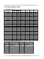
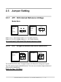
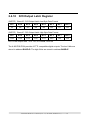
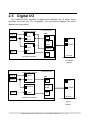
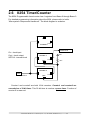
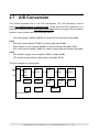
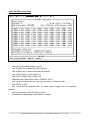
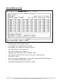
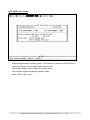
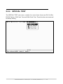
1
A-821PG
Hardware User’s Manual
Warranty
All products manufactured by ICP DAS are warranted against defective
materials for a period of one year from the date of delivery to the original purchaser.
Warning
ICP DAS assume no liability for damages consequent to the use of this
product. ICP DAS reserves the right to change this manual at any time without
notice. The information furnished by ICP DAS is believed to be accurate and reliable.
However, no responsibility is assumed by ICP DAS for its use, nor for any
infringements of patents or other rights of third parties resulting from its use.
Copyright
Copyright 1997 by ICP DAS. All rights are reserved.
Trademark
The names used for identification only may be registered trademarks of their
respective companies.
License
The user can use, modify and backup this software on a single machine. The
user may not reproduce, transfer or distribute this software, or any copy, in whole or
in part.
A-821PGL/PGH User’s Manual( Ver.2.5, Jun/2009, IMH-001-25 ) ---------1
Tables of Contents
1.
Introduction ___________________________________________________________ 4
1.1
General Description ___________________________________________________ 4
1.2
Features _____________________________________________________________ 4
1.3
Specifications _________________________________________________________ 5
1.3.1
1.4
2.
Applications _______________________________________________________________ 6
Product Check List ____________________________________________________ 6
Hardware Configuration ________________________________________________ 7
2.1
Board Layout_________________________________________________________ 7
2.2
I/O Base Address Setting ___________________________________________________ 8
2.2.1 Base Address Table ______________________________________________________________ 9
2.3
Jumper Setting ______________________________________________________ 10
2.3.1
JP1 : D/A Internal Reference Voltage Selection____________________________________ 10
2.3.2
JP3 : Single-ended/Differential Selection _______________________________________ 10
2.4
I/O Register Address__________________________________________________ 11
2.4.1 8254 Counter __________________________________________________________________ 12
2.4.2
A/D Input Buffer Register_______________________________________________________ 12
2.4.3
D/A Output Latch Register ______________________________________________________ 13
2.4.4
D/I Input Buffer Register _______________________________________________________ 13
2.4.5
Clear Interrupt Request _________________________________________________________ 14
2.4.6
A/D Gain Control Register ______________________________________________________ 14
2.4.7
A/D Multiplex Control Register __________________________________________________ 15
2.4.8
A/D Mode Control Register _____________________________________________________ 16
2.4.9
A/D Software Trigger Control Register ____________________________________________ 17
2.4.10
D/O Output Latch Register _____________________________________________________ 18
2.5
Digital I/O __________________________________________________________ 19
2.6
8254 Timer/Counter ______________________________________________________ 20
2.7
A/D Conversion __________________________________________________________ 21
2.7.1
A/D conversion flow___________________________________________________________ 22
2.7.2
A/D Conversion Trigger Modes __________________________________________________ 22
2.7.3
A/D Transfer Modes ___________________________________________________________ 23
2.7.4
Using software trigger and polling transfer _________________________________________ 23
2.8
D/A Conversion __________________________________________________________ 24
A-821PGL/PGH User’s Manual( Ver.2.5, Jun/2009, IMH-001-25 ) ---------2
3
4.
5
2.9
Analog Input Signal Connection ____________________________________________ 25
2.10
Using DB-8225 CJC Output_______________________________________________ 29
Connector ____________________________________________________________ 30
3.1
CN1/CN2/CN3 Pin Assignment _____________________________________________ 30
3.2
Daughter Board__________________________________________________________ 33
3.2.1
DB-8225 __________________________________________________________________ 33
3.2.2
DB-37 ____________________________________________________________________ 33
3.2.3
DB-16P ___________________________________________________________________ 33
3.2.4
DB-16R___________________________________________________________________ 33
Calibration ___________________________________________________________ 34
4.1
Calibration VR Description ________________________________________________ 34
4.2
D/A Calibration Steps _____________________________________________________ 34
4.3
A/D Calibration Steps _____________________________________________________ 35
Diagnostic Utility_______________________________________________________ 36
5.1
Introduction _____________________________________________________________ 36
5.2
Running Diagnostic Utility _________________________________________________ 38
5.2.1
Setup _______________________________________________________________________ 39
5.2.2
CALIBRATION ______________________________________________________________ 41
5.2.3
FUNCTION TEST ____________________________________________________________ 42
5.2.4
SPECIAL TEST ______________________________________________________________ 50
5.2.5
Help________________________________________________________________________ 51
A-821PGL/PGH User’s Manual( Ver.2.5, Jun/2009, IMH-001-25 ) ---------3
1.
Introduction
1.1 General Description
The A-821PGL/PGH is a high performance, multifunction analog, digital I/O
board for the PC AT compatible computer. The A-821PGL provides low gain (1, 2, 4,
8). The A-821PGH provides high gain (1,10,100,1000). The A-821PGL/PGH
contains a 12-bit ADC with up to 16 single-ended or 8 differential analog inputs. The
maximum sample rate of the A/D converter is about 45 k sample/sec. Also included
is a 12-bit DAC for voltage output, and 16 channels of TTL-compatible digital input,
16 channels of TTL-compatible digital output.
The NDA version of the A-821PGL provides 16 single-ended analog input or 8
channels of differential analog input. The A-821PGL NDA version doesn’t provides
analog output and digital I/O function.
1.2 Features
z
z
z
z
z
z
z
z
z
z
The maximum sample rate of the A/D converter is about 45 k sample/sec.
Software selectable input ranges
PC AT compatible ISA bus
A/D trigger mode : software trigger , pacer trigger
16 single-ended or 8 differential analog input signals
Programmable high gain : 1,10,100,1000 (A-821PGH)
Input range : ±5 V,±0.5 V,±0.05 V,±0.005 V
Programmable low gain : 1,2,4,8 (A-821PGL)
Input range : ±5 V,±2.5 V,±1.25 V,±0.625 V
1 channel 12-bit D/A voltage output (A-821PGL/PGH only)
16 digital input /16 digital output (TTL compatible) (A-821PGL/PGH only)
Interrupt handling
A-821PGL/PGH User’s Manual( Ver.2.5, Jun/2009, IMH-001-25 ) ---------4
1.3 Specifications
A-821PGL / PGH provides Analog input, Analog output and Digital I/O functions
A-821PGL/NDA version provides analog input function only
Model Name
Analog Input
Channels
A/D Converter
Sampling Rate
Over voltage Protection
Input Impedance
Trigger Modes
Data Transfer
Accuracy
Zero Drift
Analog Output
Channels
Resolution
Accuracy
Output Range
Output Driving
Slew Rate
Output Impedance
Operating Mode
Digital Input
Channels
Compatibility
Input Voltage
Response Speed
Digital Output
Channels
Compatibility
Output Voltage
Output Capability
Response Speed
Timer/Counter
Channels
Resolution
Compatibility
Input Frequency
Reference Clock
General
Bus Type
I/O Connector
Dimensions (L x W x D)
Power Consumption
Operating Temperature
Storage Temperature
Humidity
A-821PGH/PGL
16 single-ended / 8 differential
12-bit, 8 µs conversion time
45 kS/s. max.
Continuous +/-35 Vp-p
10 MΩ/6 pF
Software, Pacer
Polling, Interrupt
0.01 % of FSR ±1 LSB @ 25 °C, ± 10 V
15 ppm/°C of FSR
1 independent
12-bit
0.01 % of FSR ± 1 LSB @ 25 °C, ± 10 V
Unipolar: 0 ~ 5 V, 0 ~10 V / Bipolar: +/-10 V
+/- 5 mA
0.6 V/µs
0.1 Ω max.
Software
16
5 V/TTL
Logic 0: 0.8 V max. / Logic 1: 2.0 V min.
1.0 MHz (Typical)
16
5 V/TTL
Logic 0: 0.4 V max. / Logic 1: 2.4 V min.
Sink: 0.8 mA @ 0.8 V / Source: -2.4 mA @ 2.0 V
1.0 MHz (Typical)
3 independent
16-bit
5 V/TTL
10 MHz max.
Internal: 2 MHz
ISA
Female DB37 x 1 / 20-pin box header x 2
160 mm x 106 mm x 22 mm
300 mA @ +5 V
60 mA @ +12 V
30 mA @ -12 V
0 ~ 60 °C
-20 ~ 70 °C
5 ~ 85% RH, non-condensing
A-821PGL/PGH User’s Manual( Ver.2.5, Jun/2009, IMH-001-25 ) ---------5
z
Analog Input Range : (software programmable)
Model
A-821PGL (Low-Gain)
Gain
Bipolar (V)
Sampling
Rate Max.
Model
0.5
1
2
4
8
+/- 10
+/- 5
+/- 2.5
+/- 1.25
+/- 0.625
45 kS/s
A-821PGH (High-Gain)
Gain
Bipolar (V)
Sampling
Rate Max.
0.5
1
10
100
1000
+/- 10
+/- 5
+/- 0.5
+/- 0.05
+/- 0.005
10 kS/s
1 kS/s
45 kS/s
Note:A-821PGL/NDA version without this function
1.3.1 Applications
z
z
z
z
z
z
z
z
Signal analysis
FFT & frequency analysis
Transient analysis
Production test
Process control
Vibration analysis
Energy management
Industrial and lab. measurement and control
1.4 Product Check List
The package includes the following items:
z One piece of A-821PGL/PGH multifunction card
z One company CD
z One Quick Start Guide
Attention !
If any of these items are missing or damaged, contact the dealer who provided
you with this product. Save the shipping materials and carton in case you want
to ship or store the product in the future.
A-821PGL/PGH User’s Manual( Ver.2.5, Jun/2009, IMH-001-25 ) ---------6
2.
Hardware Configuration
2.1 Board Layout
A-821PGL/PGH
CN3
D/O
CN2
D/I
SW1
ISA BUS
JP1
JP2
VR1/2/3/4/5
ISA BUS
JP3
CN1
A-821PGL/PGH User’s Manual( Ver.2.5, Jun/2009, IMH-001-25 ) ---------7
2.2 I/O Base Address Setting
The A-821PGL/PGH occupies 16 consecutive locations in I/O address space.
The base address is set by DIP switch SW1. The default address is 0x220.
A9
A8
A7
A6
A5
A4
1
2
3
4
5
6
ON
SW1
Default Base Address 220 Hex
For Example
How to select 2 2 0 (Hex)
OFF Æ 1
ON Æ 0
2
2
0
OFF
ON
ON
ON
OFF
ON
1
0
0
0
1
0
A9
A8
A7
A6
A5
A4
The detail SW1 base addresses setting. Please refer to 2.2.1 Base
Address Table.
A-821PGL/PGH User’s Manual( Ver.2.5, Jun/2009, IMH-001-25 ) ---------8
2.2.1 Base Address Table
(*): Default base address
Base Adders
1
A9
2
A8
3
A7
4
A6
5
A5
6
A4
200-20F
210-21F
220-22F (*)
230-23F
240-24F
250-25F
260-26F
270-27F
280-28F
290-29F
2A0-2AF
2B0-2BF
2C0-2CF
2D0-2DF
2E0-2EF
2F0-2FF
OFF
OFF
OFF
OFF
OFF
OFF
OFF
OFF
OFF
OFF
OFF
OFF
OFF
OFF
OFF
OFF
ON
ON
ON
ON
ON
ON
ON
ON
ON
ON
ON
ON
ON
ON
ON
ON
ON
ON
ON
ON
ON
ON
ON
ON
OFF
OFF
OFF
OFF
OFF
OFF
OFF
OFF
ON
ON
ON
ON
OFF
OFF
OFF
OFF
ON
ON
ON
ON
OFF
OFF
OFF
OFF
ON
ON
OFF
OFF
ON
ON
OFF
OFF
ON
ON
OFF
OFF
ON
ON
OFF
OFF
ON
OFF
ON
OFF
ON
OFF
ON
OFF
ON
OFF
ON
OFF
ON
OFF
ON
OFF
300-30F
310-31F
320-32F
330-33F
340-34F
350-35F
360-36F
370-37F
380-38F
390-39F
3A0-3AF
3B0-3BF
3C0-3CF
3D0-3DF
3E0-3EF
3F0-3FF
OFF
OFF
OFF
OFF
OFF
OFF
OFF
OFF
OFF
OFF
OFF
OFF
OFF
OFF
OFF
OFF
OFF
OFF
OFF
OFF
OFF
OFF
OFF
OFF
OFF
OFF
OFF
OFF
OFF
OFF
OFF
OFF
ON
ON
ON
ON
ON
ON
ON
ON
OFF
OFF
OFF
OFF
OFF
OFF
OFF
OFF
ON
ON
ON
ON
OFF
OFF
OFF
OFF
ON
ON
ON
ON
OFF
OFF
OFF
OFF
ON
ON
OFF
OFF
ON
ON
OFF
OFF
ON
ON
OFF
OFF
ON
ON
OFF
OFF
ON
OFF
ON
OFF
ON
OFF
ON
OFF
ON
OFF
ON
OFF
ON
OFF
ON
OFF
The PC I/O port mapping is given below.
ADDRESS
000-1FF
200-20F
210-21F
238-23F
278-27F
2B0-2DF
2E0-2E7
2E8-2EF
2F8-2FF
300-31F
Device
PC reserved
Game/control
XT Expansion Unit
Bus Mouse/Alt. Bus Mouse
Parallel Printer
EGA
AT GPIB
Serial Port
Serial Port
Prototype Card
ADDRESS
320-32F
378-37F
380-38F
3A0-3AF
3B0-3BF
3C0-3CF
3D0-3DF
3E8-3EF
3F0-3F7
3F8-3FF
Device
XT Hard Disk
Parallel Printer
SDLC
SDLC
MDA/Parallel Printer
EGA
CGA
Serial Port
Floppy Disk
Serial Port
A-821PGL/PGH User’s Manual( Ver.2.5, Jun/2009, IMH-001-25 ) ---------9
2.3 Jumper Setting
2.3.1
JP1 : D/A Internal Reference Voltage
Selection
Reference
Reference
Voltage
J1
-5 V
(default)
J2
(-10 V)
Voltage
J1
-10 V
J2
(-5 V)
Select (-5 V) : D/A voltage output = 0 ~ 5 V (both channel)
Select (-10 V): D/A voltage output = 0 ~ 10 V (both channel)
JP1 is valid only if JP2 selects D/A internal reference voltage
2.3.2
JP3 : Single-ended/Differential Selection
Single-ended
SINGLE
Differential
SINGLE
(default)
DIFF
DIFF
The A-821PGL/PGH offers 16 single-ended or 8 differential analog input signals.
The JP3 selects single-ended/differential. The user can not select single-ended and
differential simultaneously.
Refer to Sec. 2.9 first.
A-821PGL/PGH User’s Manual( Ver.2.5, Jun/2009, IMH-001-25 ) ---------10
2.4 I/O Register Address
The A-821PGL/PGH occupies 16 consecutive PC I/O addresses.
The following table lists the registers and their locations.
Address
Read
Write
Base+0
Reserved
Reserved
Base+1
8254 Counter 1
8254 Counter 1
Base+2
8254 Counter 2
8254 Counter 2
Base+3
Reserved
8254 Counter Control
Base+4
A/D Low Byte
D/A Channel 0 Low Byte
Base+5
A/D High Byte
D/A Channel 0 High Byte
Base+6
DI Low Byte
Reserved
Base+7
DI High Byte
Reserved
Base+8
Reserved
A/D Clear Interrupt Request
Base+9
Reserved
A/D Gain Control
Base+A
Reserved
A/D Multiplexer Control
Base+B
Reserved
A/D Mode Control
Base+C
Reserved
A/D Software Trigger Control
Base+D
Reserved
DO Low Byte
Base+E
Reserved
DO High Byte
Base+F
Reserved
Reserved
A-821PGL/PGH User’s Manual( Ver.2.5, Jun/2009, IMH-001-25 ) ---------11
2.4.1 8254 Counter
The 8254 Programmable timer/counter has 4 registers from Base+0 through Base+3.
For detailed programming information about the 8254, please refer to Intel‘s
“Microsystem Components Handbook”.
Address
Read
Write
Base+1
8254 Counter 1
8254 Counter 1
Base+2
8254 Counter 2
8254 Counter 2
Base+3
Reserved
8254 Counter Control
2.4.2 A/D Input Buffer Register
(READ)
Base+4 : A/D Low Byte Data Format
Bit 7
Bit 6
Bit 5
Bit 4
Bit 3
Bit 2
Bit 1
Bit 0
D7
D6
D5
D4
D3
D2
D1
D0
(READ)
Base+5 : A/D High Byte Data Format
Bit 7
Bit 6
Bit 5
Bit 4
Bit 3
Bit 2
Bit 1
Bit 0
0
0
0
BUSY
D11
D10
D9
D8
A/D 12 bits data : D11…D0, D11=MSB, D0=LSB
BUSY =1 : A/D 12 bits of data busy
=0 : A/D 12 bits of data ready
The low 8 bits of A/D data are stored in address BASE+4 and the high 4 bits of data
are stored in address BASE+5. The BUSY bit is used as an indicator for A/D
conversion. When an A/D conversion is completed, the BUSY bit will be cleared
to zero.
A-821PGL/PGH User’s Manual( Ver.2.5, Jun/2009, IMH-001-25 ) ---------12
2.4.3 D/A Output Latch Register
(WRITE)
Base+4 : Channel 1 D/A Low Byte Data Format
Bit 7
Bit 6
Bit 5
Bit 4
Bit 3
Bit 2
Bit 1
Bit 0
D7
D6
D5
D4
D3
D2
D1
D0
(WRITE)
Base+5 :Channel 1 D/A High Byte Data Format
Bit 7
Bit 6
Bit 5
Bit 4
Bit 3
Bit 2
Bit 1
Bit 0
X
X
X
X
D11
D10
D9
D8
D/A 12 bits of output data : D11..D0, D11=MSB, D0=LSB, X=don‘t care
The D/A converter will convert the 12 bits of digital data to analog output. The low 8
bits of D/A channel are stored in address BASE+4 and high 4 bits are stored in
address BASE+5. The D/A output latch registers are designed as a “double
buffered” structure, so the analog output latch registers will be updated until the
high 4 bits of digital data are written. the user must send low 8 bits first and then
send high 4 bits to update the 12 bits AD output latch register.
NOTE : Send low 8 bits first, then send high 4 bits.
2.4.4 D/I Input Buffer Register
(READ)
Base+6 : D/I Input Buffer Low Byte Data Format
Bit 7
Bit 6
Bit 5
Bit 4
Bit 3
Bit 2
Bit 1
Bit 0
D7
D6
D5
D4
D3
D2
D1
D0
(READ)
Base+7 : D/I Input Buffer High Byte Data Format
Bit 7
Bit 6
Bit 5
Bit 4
Bit 3
Bit 2
Bit 1
Bit 0
D15
D14
D13
D12
D11
D10
D9
D8
D/I 16 bits of input data : D15..D0, D15=MSB, D0=LSB
The A-821PGL/PGH provides 16 TTL compatible digital inputs. The low 8 bits are
stored in address BASE+6. The high 8 bits are stored in address BASE+7.
A-821PGL/PGH User’s Manual( Ver.2.5, Jun/2009, IMH-001-25 ) ---------13
2.4.5
Clear Interrupt Request
(WRITE)
Base+8 : Clear Interrupt Request Format
Bit 7
Bit 6
Bit 5
Bit 4
Bit 3
Bit 2
Bit 1
Bit 0
X
X
X
X
X
X
X
X
X=don‘t care, XXXXXXXX=any 8 bits of data are valid
If the A-821PGL/PGH is working in the interrupt transfer mode, an on-board
hardware status bit will be set after each A/D conversion. This bit must be cleared
by software before the next hardware interrupt. Writing any value to address
BASE+8 will clear this hardware bit and the hardware will generate another interrupt
when the next A/D conversion is completed.
2.4.6 A/D Gain Control Register
(WRITE)
Base+9 : A/D Gain Control Register Format
Bit 7
Bit 6
Bit 5
Bit 4
Bit 3
Bit 2
Bit 1
Bit 0
X
X
X
X
X
X
GAIN1
GAIN0
The Only difference between the A-821PGL and the A-821PGH is the GAIN control
function. The A-821PGL provides a gain factor of 1/2/4/8 and the A-821PGH
provides 1/10/100/1000. The gain control register controls the gain of the A/D
input signal. Bipolar/Unipolar will affect the gain factor.
It is important to select the correct gain-control-code according to Bipolar/Unipolar
input.
NOTE : If the gain control code is changed, the hardware needs to delay
extra gain settling time. The gain settling time is different for different gain control
code. The dos software driver does not control the gain settling time, so the
user must delay the gain settling time if the gain is changed.
A-821PGL/PGH User’s Manual( Ver.2.5, Jun/2009, IMH-001-25 ) ---------14
A-821PGL GAIN CONTROL CODE TABLE
GAIN
Input Range
GAIN1 GAIN0
Settling Time
1
+/- 5 V
0
0
23 μs
2
+/- 2.5 V
0
1
23 μs
4
+/- 1.25 V
1
0
25 μs
8
+/- 0.625 V
1
1
28 μs
A-821PGH GAIN CONTROL CODE TABLE
GAIN
Input Range
GAIN1 GAIN0
Settling Time
1
+/- 5 V
0
0
23 μs
10
+/- 0.5 V
0
1
28 μs
100
+/- 0.05 V
1
0
140 μs
1000
+/- 0.005 V
1
1
1300 μs
2.4.7 A/D Multiplex Control Register
(WRITE)
Base+A : A/D Multilexer Control Register Format
Bit 7
Bit 6
Bit 5
Bit 4
Bit 3
Bit 2
Bit 1
Bit 0
X
X
X
X
D3
D2
D1
D0
A/D input channel selection data = 4 bits : D3...D0, D3=MSB, D0=LSB, X=don‘t care
Single-ended mode : D3..D0
Differential mode : D2..D0, D3=don’t care
The A-821PGL/PGH provides 16 single-ended or 8 differential analog input signals.
In single-ended mode, D3~D0 selects the active channel. In differential mode,
D2~D0 selects the active channel and D3 will be “X” (don’t care).
NOTE: The settling time of the multiplexer depends on the source resistance of input
sources.
source resistance = about 0.1kOhm
source resistance = about 1 kOhm
source resistance = about 10 kOhm
source resistance = about 100 kOhm
Æ
Æ
Æ
Æ
settling time = about 3 μs.
settling time = about 5 μs.
settling time = about 10 μs.
settling time = about 100 μs.
Sec 2.4.6 gives information about how to delay the settling time.
A-821PGL/PGH User’s Manual( Ver.2.5, Jun/2009, IMH-001-25 ) ---------15
2.4.8 A/D Mode Control Register
(WRITE)
Base+B : A/D Mode Control Register Format
Bit 7
Bit 6
Bit 5
Bit 4
Bit 3
Bit 2
Bit 1
Bit 0
X
SI2
SI1
SI0
X
D2
D1
D0
X=don‘t care
Mode Select
D2 D1
Trigger Type
Transfer Type
D0
Software Trig
Pacer Trig
Software
Interrupt
0
0
0
Select
X
Select
X
0
0
1
Select
X
Select
X
0
1
0
X
Select
X
X
1
1
0
X
Select
Select
Select
X=disable
SI2
SI1
SI0
IRQ Level
0
0
0
IRQ2
0
0
1
Not Used
0
1
0
IRQ2
0
1
1
IRQ3
1
0
0
IRQ4
1
0
1
IIRQ5
1
1
0
IRQ6
1
1
1
IRQ7
The A/D conversion operation can be divided into 2 stages, trigger stage and
transfer stage. The trigger stage will generate a trigger signal to the A/D converter
and the transfer stage will transfer the result to the CPU.
The trigger method may be Software trigger or Pacer trigger.
The software
trigger is very simple but cannot control the sampling rate precisely. In
software trigger mode, the program issues a software trigger command (sec 2.4.9)
any time needed. Then the program will poll the A/D status bit until the busy bit is
0(sec 2.4.2).
A-821PGL/PGH User’s Manual( Ver.2.5, Jun/2009, IMH-001-25 ) ---------16
The pacer trigger can control the sampling rate very precisely. So the
converted data can be used to reconstruct the waveform of the analog input
signal. In pacer trigger mode, the pacer timer (sec 2.6) will periodically generate
trigger signals to the A/D converter. These converted data can be transfer to the
CPU by polling or interrupt.
The software driver provides polling or interrupt transfer. The polling
subroutine, A-822_AD_PollingVar() or A-822_AD_PollingArray(), sets the A/D mode
control register to 0x01. This control word means software trigger and polling
transfer. The interrupt subroutine, A-822_AD_INT_START(…), sets the A/D mode
control mode register to 0x06. This control word means pacer trigger and interrupt
transfer.
2.4.9 A/D Software Trigger Control Register
(WRITE)
Base+C : A/D Software Trigger Control Register Format
Bit 7
Bit 6
Bit 5
Bit 4
Bit 3
Bit 2
Bit 1
Bit 0
X
X
X
X
X
X
X
X
X=don‘t care, XXXXXXXX=any 8 bits data is validate
The A/D converter can be triggered by software trigger or pacer trigger.
Detailed information is given in sec. 2.4.8 and sec. 2.7. Writing any value to address
BASE+C will generate a trigger pulse to A/D converter and initiate an A/D
conversion operation. The address BASE+5 offers a busy bit to indicate an A/D
conversion has been complete.
The software driver uses this control word to detect the A-821PGL/PGH
hardware board. The software initiates a software trigger and checks the busy
bit. If the busy bit cannot clear to zero in a fixed time, the software driver will return
an error message. If there is an I/O BASE address setting error, the busy bit will not
be cleared to zero. The software driver, A-821_CheckAddress(), uses this method
to detect the correctness of the I/O BASE address setting
A-821PGL/PGH User’s Manual( Ver.2.5, Jun/2009, IMH-001-25 ) ---------17
2.4.10 D/O Output Latch Register
(WRITE)
Base+D : D/O Output Latch Low Byte Data Format
Bit 7
Bit 6
Bit 5
Bit 4
Bit 3
Bit 2
Bit 1
Bit 0
D7
D6
D5
D4
D3
D2
D1
D0
(WRITE)
Base+E : D/O Output Latch High Byte Data Format
Bit 7
Bit 6
Bit 5
Bit 4
Bit 3
Bit 2
Bit 1
Bit 0
D15
D14
D13
D12
D11
D10
D9
D8
D/O 16 bits output data : D15...D0, D15=MSB, D0=LSB
The A-821PGL/PGH provides 16 TTL compatible digital outputs. The low 8 bits are
stored in address BASE+D. The high 8 bits are stored in address BASE+E
A-821PGL/PGH User’s Manual( Ver.2.5, Jun/2009, IMH-001-25 ) ---------18
2.5 Digital I/O
The A-821PGL/PGH provides 16 digital input channels and 16 digital output
channels. All levels are TTL compatible. The connections diagram and block
diagram are given below:
Input Buffer Register
CN2
Base+6
Read
D0..D7
A-821PGL/PGH
1..8
D0..D7
DI
17..18
DGND
DGND
D8..D15
Base+7
Strobe 20
Read
9..16
TB-9182
Input Buffer Register
16 Channel Isolation
Input Board
(Option)
Output Buffer Register
Base+D
A-821PGL/PGH
Read
CN3
D0..D7
D0..D7
1..8
DO
17..18
D8..D15
Base+E
Read
Output Buffer Register
DGND
DGND
9..16
TB-9185
16 Channel Relay Output
Board
(Option)
A-821PGL/PGH User’s Manual( Ver.2.5, Jun/2009, IMH-001-25 ) ---------19
2.6 8254 Timer/Counter
The 8254 Programmable timer/counter has 4 registers from Base+0 through Base+3.
For detailed programming information about the 8254, please refer to Intel‘s
“Microsystem Components Handbook”. The block diagram is as below.
Gate
Cin
Cout
Counter 0
PACER CLK
Cin : clock input
Cout : clock output
INTCLK : internal clock
VCC
Counter 1
Cin
Gate
Cout
10 k
Counter 2
2 MHz
INTCLK
Cin
Gate
Cout
Counter1 and counter2 are both 16-bit counters. Counter1 and counter2 are
cascaded as a 32-bit timer. This 32-bit timer is used as a pacer timer. Function of
counter 0 is reserved.
A-821PGL/PGH User’s Manual( Ver.2.5, Jun/2009, IMH-001-25 ) ---------20
2.7 A/D Conversion
This section explains how to use A/D conversions. The A/D conversion can be
active by software trigger or pacer trigger. At the end of the A/D conversion, it is
possible to transfer data by polling and interrupt. Before using the A/D conversion
function, users should notice the following issues:
*
A/D data register, BASE+4/BASE+5, stores the A/D conversion data (sec.
2.4.2)
*
A/D gain control register, BASE+9, selects gain (sec. 2.4.6)
*
A/D multiplex control register, BASE+A, selects analog input (sec. 2.4.7)
*
A/D mode control register, BASE+B, selects trigger type and transfer type (sec.
2.4.8)
*
A/D software trigger control register, BASE+C (sec. 2.4.9)
*
JP3 selects single-ended or differential input (sec. 2.3.3)
The block diagram is given below:
CN3
16/8 to 1
Gain
12 bits
Multi-
control
A/D
Buffer
Memory
Base+9
Trigger
Transfer
CPU
Logic
Logic
plexer
Base+A
JP3
Base+C
Base+B
A-821PGL/PGH
A-821PGL/PGH User’s Manual( Ver.2.5, Jun/2009, IMH-001-25 ) ---------21
2.7.1
A/D conversion flow
Next, the user must decide which A/D conversion mode will be used. The
software driver supports polling or interrupt mode. The user can control the A/D
conversion by polling mode very easily (sec. 2.4.9). It is recommended to use the
software driver if using interrupt mode
The analog input signals come from CN1. These signals may be single-ended or
differential type and must match with the setting of JP3.
The multiplexer can select 16 single-ended or 8 differential signals into the gain
control module. The gain control module also needs settling time if the gain control
code is changed. Because the dos software doesn’t manage the settling time, the
user should delay enough settling time to accommodate for gain control code
changes. (sec. 2.4.6)
The output of the gain control module feeds into the A/D converter. The A/D
converter needs a trigger signal to start the A/D conversion cycle. The
A-821PGL/PGH supports software trigger or pacer trigger mode.
2.7.2 A/D Conversion Trigger Modes
The A-821PGL/PGH supports two trigger modes.
1 : Software Trigger :
Writes any value to A/D software trigger control register, BASE+C, will initiate
an A/D conversion cycle. This mode is very simple but very difficult to control
the sampling rate.
2 : Pacer Trigger Mode :
The block diagram of the pacer timer is shown in section 2.6. The pacer timer
gives very precise sampling rates.
A-821PGL/PGH User’s Manual( Ver.2.5, Jun/2009, IMH-001-25 ) ---------22
2.7.3
A/D Transfer Modes
A-821PGL/PGH supports two transfer modes.
Polling transfer :
This mode can be used with both trigger modes. Detailed information is given in
section 2.4.8. The software scans A/D high byte data register, BASE+5, until
BUSY_BIT=0.The low byte data is also ready in BASE+4.
Interrupt transfer :
This mode can be used with the pacer trigger. Detailed information is given in
section 2.4.8. The user can set the IRQ level by using software (Base+B). A
hardware interrupt signal is sent to the PC when an A/D conversion is
completed.
2.7.4 Using software trigger and polling transfer
If the user needs to direct control the A/D converter without the A-821 software
driver. It is recommended to use software trigger and polling transfer. The program
steps are listed as below:
1. send 0x01 to A/D mode control register (software trigger + polling transfer)
(refer to Sec. 2.4.8)
2. send channel number to multiplexer control register (refer to Sec. 2.4.7)
3. send the gain control code value to gain control register (refer to Sec 2.4.6)
4. delay the settling time (refer to Sec. 2.4.6 and Sec. 2.4.7)
5. send any value to software trigger control register to generate a software trigger
signal
(refer to Sec. 2.4.9)
6. scan the BUSY bit of the A/D high byte data until BUSY=0 (refer to Sec. 2.4.2)
7. read the 12 bits A/D data (refer to Sec. 2.4.2)
8. convert this 12 bits binary data to floating point value
(refer to “A-821 DOS Software Manual, Sec. 4.7 and Sec. 4.8)
A-821PGL/PGH User’s Manual( Ver.2.5, Jun/2009, IMH-001-25 ) ---------23
2.8 D/A Conversion
The A-821PGL/PGH provides two 12-bit D/A converters. Before using the D/A
conversion function, users should notice the following issues:
*
D/A output register, BASE+4/ BASE+5 (sec. 2.4.3)
*
JP1/JP2 select internal reference voltage -5 V/-10 V (sec. 2.3.1)
NOTE : The DA output latch registers are designed as “double buffer” structure.
The user must send the low byte data first, then send the
high byte data to store the DA 12-bit digital data. If the user only
sends the high byte data, then the low byte data will still be the previous value. Also,
if the user sends high byte first then sends low byte, the low byte data of DA are still
held in the previous one.
A-821PGL/PGH User’s Manual( Ver.2.5, Jun/2009, IMH-001-25 ) ---------24
2.9 Analog Input Signal Connection
The A-821PGL/PGH can measure single-ended or differential type analog input
signals. Some analog signals can be measured in both single-end and differential
mode, but some can only be measured in either single-ended or differential mode.
The user must decide which mode is suitable for measurement.
In general, there are 3 different analog signal connection methods as shown in
Fig1 to Fig3. Fig1 is suitable for grounding source analog input signals. Fig2 can
measure more channels than Fig1, but is only suitable for large analog input signals.
Fig3 is suitable for thermocouple and Fig4 is suitable for floating source analog input
signals.
Note : In Fig3, the maximum common mode voltage between the analog
input source and the AGND is 70 Vp-p, so the user must make sure that the
input signal is under specification first. If the common mode voltage is over 70
Vp-p, the input multiplexer will be damaged forever.
The simple way to select the input signal connection configuration is as below.
1.
2.
3.
4.
Grounding source input signal
Æ select Fig1
Thermocouple input signal
Æ select Fig3
Floating source input signal
Æ select Fig4
If Vin > 0.1 V and gain<=10 (Low gain)
and more channels are needed Æselect Fig2
If the user is not able to determine the characteristics of the input signal, the test
steps are given as below:
1.
2.
3.
4.
Step1 : try Fig1 and record the measurement results
Step2 : try Fig4 and record the measurement results
Step3 : try Fig2 and record the measurement results
Compare the measurement results of step1, step2,
step3 and select the best one
A-821PGL/PGH User’s Manual( Ver.2.5, Jun/2009, IMH-001-25 ) ---------25
1. FG1 : Connecting to grounding source input (Right way)
A-821PGL/PGH
A/D CH0HI
Es1
A/D CH0LO
GND1
AGND
A/D CHnHI
Esn
A/D CHnLO
GNDn
AGND
FG1 : Wrong way
A/D CH0HI
Es1
A/D CH0LO
GND1
AGND
A/D CHnHI
Esn
A/D CHnLO
GNDn
AGND
A-821PGL/PGH User’s Manual( Ver.2.5, Jun/2009, IMH-001-25 ) ---------26
FG2 : Connecting to singled-ended input configuration
A-821PGL/PGH
A/D CH0
A/D CHn
Es
AGND
CAUTION : The maximum common mode voltage between the
analog input source and the AGND is 70 Vp-p, so the user must make sure
that the input signal is under specification first. If the common mode voltage
is over 70 Vp-p, the input multiplexer will be damaged forever.
A-821PGL/PGH User’s Manual( Ver.2.5, Jun/2009, IMH-001-25 ) ---------27
FG3 : connecting to floating source configuration
A-821PGL/PGH
A/D CH0HI
Es
A/D CH0LO
AGND
A/D CHnHI
Esn
A/D CHnLO
AGND
Signal Shielding
*
*
Signal shielding connections in Fig1 to Fig4 are all the same
Use single-point connection to frame ground (not AGND or DGND)
A-821PGL/PGH
Vin
AGND
DGND
Frame Ground
A-821PGL/PGH User’s Manual( Ver.2.5, Jun/2009, IMH-001-25 ) ---------28
2.10 Using DB-8225 CJC Output
The DB-8225 daughter board with built-in CJC Circuitry, provided with the
A-821PGL/PGH, produces 10 mV per Deg C With 0.0 Volts @ -273 Deg C.
The A-821 should be protected from draughts and direct sunlight in order to
accurately reflect room temperature.
CJC Calibration:
1. Connect the A-821PGL/PGH to DB-8215 CN1
2. Set the A-821PGL/PGH to Single-ended Mode
3. Set JP1 to 1-2 and JP2 to 2-3 ( Single-ended mode)
4. Read the temperature from a digital thermometer placed near D1/D2
(See DB-8225 layout).
5.Read the A-821PGL/PGH analog input channel 0 (single-ended channel 0)
6.Adjust VR1 until a stable reading of 10 mV per deg C is attained.
For example, when the environment temperature is 24 deg C. the reading value
of CJC will be 2.97 V
(273 deg c +24 deg c ) X 10 mV/deg c
= 2.97 V
You should use an A/D Channel for CJC calibration. AI0 is reserved for the
CJC calibration used in single ended mode and CH0-HI & CH0-LO are reserved
for differential mode. It is recommended to use differential mode if measuring
thermocouple.
A-821PGL/PGH User’s Manual( Ver.2.5, Jun/2009, IMH-001-25 ) ---------29
3
Connector
The A-821PGL/PGH provides three connectors: CN2 for 16 bits
digital input, CN3 for 16 digital output and CN1 for analog input,
analog output.
3.1 CN1/CN2/CN3 Pin Assignment
CN2 : Digital Input Connector Pin Assignment
Pin Number
Description
Pin Number
Description
1
Digital Input 0/TTL
2
Digital Input 1/TTL
3
Digital Input 2/TTL
4
Digital Input 3/TTL
5
Digital Input 4/TTL
6
Digital Input 5/TTL
7
Digital Input 6/TTL
8
Digital Input 7/TTL
9
Digital Input 8/TTL
10
Digital Input 9/TTL
11
Digital Input 10/TTL
12
Digital Input 11/TTL
13
Digital Input 12/TTL
14
Digital Input 13/TTL
15
Digital Input 14/TTL
16
Digital Input 15/TTL
17
PCB‘s
GND output
18
PCB‘s
19
PCB‘s
+5 V output
20
STROBE
GND output
CN3 : Digital Output Connector Pin Assignment
Pin Number
Description
Pin Number
Description
1
Digital Output 0/TTL
2
Digital Output 1/TTL
3
Digital Output 2/TTL
4
Digital Output 3/TTL
5
Digital Output 4/TTL
6
Digital Output 5/TTL
7
Digital Output 6/TTL
8
Digital Output 7/TTL
9
Digital Output 8/TTL
10
Digital Output 9/TTL
11
Digital Output 10/TTL
12
Digital Output 11/TTL
13
Digital Output 12/TTL
14
Digital Output 13TL
15
Digital Output 14/TTL
16
Digital Output 15/TTL
17
PCB‘s
GND output
18
PCB‘s
GND output
19
PCB‘s
+5 V output
20
PCB‘s
+12 V output
A-821PGL/PGH User’s Manual( Ver.2.5, Jun/2009, IMH-001-25 ) ---------30
FOR SINGLE-ENDED SIGNALS
CN1 : Analog input/Analog output Connector Pin Assignment.
Pin Number
Description
Pin Number
Description
1
Analog Input 0/+
20
Analog Input 8/+
2
Analog Input 1/+
21
Analog Input 9/+
3
Analog Input 2/+
22
Analog Input 10/+
4
Analog Input 3/+
23
Analog Input 11/+
5
Analog Input 4/+
24
Analog Input 12/+
6
Analog Input 5/+
25
Analog Input 13/+
7
Analog Input 6/+
26
Analog Input 14/+
8
Analog Input 7/+
27
Analog Input 15/+
9
Analog GND
28
Analog GND
10
Analog GND
29
Analog GND
11
Not Used
30
D/A channel 0‘s analog voltage
output
12
Not Used
31
Not Used
13
PCB‘s
32
Not Used
14
Analog GND
33
Not Used
15
Digital GND
34
Not Used
16
Not Used
35
Not Used
17
Not Used
36
Not Used
18
Not Used
37
Not Used
19
PCB‘s
+12 V output
+5 V output
A-821PGL/PGH User’s Manual( Ver.2.5, Jun/2009, IMH-001-25 ) ---------31
FOR DIFFERENTIAL SIGNALS
CN1 : Analog input/Analog output Connector Pin Assignment
Pin Number
Description
Pin Number
Description
1
Analog Input 0/+
20
Analog Input 0/-
2
Analog Input 1/+
21
Analog Input 1/-
3
Analog Input 2/+
22
Analog Input 2/-
4
Analog Input 3/+
23
Analog Input 3/-
5
Analog Input 4/+
24
Analog Input 4/-
6
Analog Input 5/+
25
Analog Input 5/-
7
Analog Input 6/+
26
Analog Input 6/-
8
Analog Input 7/+
27
Analog Input 7/-
9
Analog GND
28
Analog GND
10
Analog GND
29
Analog GND
11
Not used
30
D/A channel 0‘s analog voltage
output
12
Not used
31
Not used
13
PCB‘s
32
Not used
14
Analog GND
33
Not used
15
Digital GND
34
Not used
16
Not used
35
Not used
17
Not used
36
Not used
18
Not used
37
Not used
19
PCB‘s
XXXXXXX
This pin not available
+12 V output
+5 V output
A-821PGL/PGH User’s Manual( Ver.2.5, Jun/2009, IMH-001-25 ) ---------32
3.2 Daughter Board
The A-821PGL/PGH can be connected with many different daughter boards. The
function of these daughter boards are described as follows.
3.2.1 DB-8225
The DB-8225 provides an on-board CJC (Cold Junction Compensation) circuit
for thermocouple measurement and terminal block for easy signal connection and
measurement. The CJC is connected to A/D channel_0. The A-821PGL/PGH can
connect CN1 directly to DB-8225 through a 37-pin D-sub connector.
3.2.2 DB-37
The DB-37 is a general purpose 37-pin connector. This board directly connects
to a 37-pin D-sub connector. It is suitable for easy signal connection and
measurement.
3.2.3 DB-16P
The DB-16P (or 782 series) is a 16 channel isolated digital input board. The
A-821PGL/PGH provides 16 channel non-isolated TTL-compatible digital inputs from
CN2. If connecting to DB-16P, the A-821PGL/PGH can provide 16 isolated digital
input channels. Isolation can protect PC if abnormal input signal is occurred.
3.2.4 DB-16R
The DB-16R (or 785 series) provides 16-channel SPDT relay output. The
A-821PGL/PGH provides 16-channel TTL-compatible digital output from CN3. If
connected to the DB-16R, the A-821PGL/PGH can provide 16-channel relay output
to control power devices.
A-821PGL/PGH User’s Manual( Ver.2.5, Jun/2009, IMH-001-25 ) ---------33
4.
Calibration
The A-821PGL/PGH is calibrated to its best state of operation. For environments
with large amount of vibration, recalibration is recommended. Before calibrating the
A-821PGL/PGH, users should take care of the following issues:
*
*
*
One 6-digit multimeter
One stable voltage source (4.9988 V)
Diagnostic program : this program included in the delivered
package will guide the user in further calibration.
4.1 Calibration VR Description
There are five VRs on the A-821PGL/PGH. Calibration needs to adjust all the VRs.
VR Num. Description
VR1
D/A Gain adjustment
VR2
D/A Offset adjustment
VR3
A/D Offset adjustment
VR4
A/D Gain adjustment
VR5
A/D PGA adjustment (Programmable Gain Amplifier )
4.2 D/A Calibration Steps
1.
2.
3.
4.
5.
6.
7.
8.
Run A82xDIAG.EXE
Press “Right Arrow Key” to select “CALIBRATION” item
Select & Execute “A. D/A Offset ” item
Connect D/A channel 0, pin 30 of CN1, to DVM
Adjust VR2 until DVM=0 V
Press “ESC Key”
Select & Execute “B. D/A REFERENCE” item
Adjust VR1 until DVM=4.9988V
A-821PGL/PGH User’s Manual( Ver.2.5, Jun/2009, IMH-001-25 ) ---------34
4.3 A/D Calibration Steps
1.
2.
3.
4.
5.
6.
7.
8.
9.
10.
11.
12.
13.
14.
15.
16.
17.
Run A-82XDIAG.EXE
Select “CARD TYPE” to A-821
Press “Right Arrow Key” to select “CALIBRATION” item
Press “Down Arrow Key” to select “C. A/D REFERENCE” item.
Press “Enter Key”
Input stable 4.9988 V to A/D channel 0, pin 1 of CN1
Adjust VR4 until A/D data shown in screen between 4094 to 4095
Press “ESC Key”
Select & Execute “D. A/D OFFSET” item
Input stable 0 V to A/D channel 0, pin1 of CN1
Adjust VR3 until A/D data shown in screen between 2048 to 2049
Press “ESC Key”
Repeat step_3 to step_11 until no need to adjust VR4,VR3
Select & Execute “E. PGA OFFSET” item
Input stable 0 V to A/D channel 0, pin 1 of CN1
Adjust VR5 until A/D data shown in screen between 2048 to 2049
Press “ESC Key”
A-821PGL/PGH User’s Manual( Ver.2.5, Jun/2009, IMH-001-25 ) ---------35
5
Diagnostic Utility
5.1 Introduction
The diagnostic utility, A-82XDIAG.EXE, is a menu-driven program which
assists the user in a complete testing of the A-821PGL/PGH board. When in doubt
regarding the operation of the A-821PGL/PGH board, run the diagnostic utility to
check the functions of the board. To run the diagnostic utility, change to the
subdirectory used in the installation process (C:\A-821 for example). Then type
"A82XDIAG" <Enter> to start. The steps are shown as following:
C:\>CD A-822 <Enter>
C:\A-821>CD DIAG <Enter>
C:\A-821\DIAG>A-821DIAG <Enter>
A configuration file, named A-82x.CFG, is associated with the A-82XDIAG.EXE.
The configuration of the A-821PGL/PGH board is recorded in this file. The
information includes the I/O base address, interrupt number and DMA channel
number used by the A-821PGL/PGH. While the A-82XDIAG is running, if you
make some adjustments, the changes will not be saved automatically. Therefore,
the user must select the save function to save the changes. When
A-82XDIAG.EXE starts up, it will automatically check if the jumper setting of the
I/O base address is identical to the value stored in the configuration file. If the
address is not identical, an error message will appear to warn you. The screen is
shown as below.
A-821PGL/PGH User’s Manual( Ver.2.5, Jun/2009, IMH-001-25 ) ---------36
Although you can continue by pressing any key, it is recommended to correct
this situation by setting the proper jumper setting. Because many operations occur
in the A-82XDIAG, the I/O base address is check first. And if the error occurs, it
doesn’t work.
A-821PGL/PGH User’s Manual( Ver.2.5, Jun/2009, IMH-001-25 ) ---------37
5.2 Running Diagnostic Utility
The initialization screen of the A-82XDIAG is shown as below. As
you can see, there are five items on the main menus in the initialization
screen. They are Setup, Calibration, FunctionTest, sPecialTest and
Help. Use the Left or Right key to select the items on the main menu.
An item that is highlighted means it is selected, and some menu items
are associated with it. Use the Up or Down key to select the sub items,
those items will also be highlighted. Alternately, the user can press the
command key to highlight the menu item. A command key in a menu
item is the character which is highlighted. To proceed with a function
associated the highlighted menu item, just press <Enter>. And press
<Esc> to abort the current function.
A-821PGL/PGH User’s Manual( Ver.2.5, Jun/2009, IMH-001-25 ) ---------38
5.2.1
Setup
“Setup” allows users to setup the board configuration. There are six functions in this
item, Card type, Base Address, DMA no, IRQ no, Save option, eXit.
Card type : <Up/Down> key to select A-821PGL/PGH, <Enter> key to select
Base Address : <Up/Down> key to select base address, <Enter> key to select
DMA no : <Up/Down> key to select DMA no, <Enter> key to select
IRQ no : <Left/Right> key to select IRQ no, <Enter> key to select
Save option : <Left/Right> key to select yes/no, <Enter> key to select
eXit : <Left/Right> key to select yes/no, <Enter> key to select
Base address selection screen.
A-821PGL/PGH User’s Manual( Ver.2.5, Jun/2009, IMH-001-25 ) ---------39
DMA no and IRQ no selection screen
A-821PGL/PGH User’s Manual( Ver.2.5, Jun/2009, IMH-001-25 ) ---------40
5.2.2
CALIBRATION
The “CALIBRATION” contains ten menu items: those are, D/A Reference voltage,
D/A Channel 0 gain, D/A channel 1 gain, A/D Gain, A/D Offset, A/D Bipolar Offset,
A/D Unipolar Offset. These items are concerning the calibration of the
A-821PGL/PGH. In CALIBRATION main menu, a graphic presentation of the
A-821PGL/PGH board's layout is shown. The calibration will become a visual
process in order to reduce user's effort. To keep the optimal performance and
correct precision for the board, it is useful to calibrate the board after working for a
long time period. There are seven VRs that need to be tuned in the calibration
process. When you highlight one of the first seven menu items, the associated VR
begins blinking. And a message window will appear to direct the user how to tune
the VRs. The main menu screen is shown as below.
A-821PGL/PGH User’s Manual( Ver.2.5, Jun/2009, IMH-001-25 ) ---------41
5.2.3
FUNCTION TEST
The FUNCTION TEST main menu contains seven menu items: those are D/A TEST,
Digital I/O, A/D MULTIPLEX, A/D use IRQ, A/D use DMA, A/D GAIN, Timer 0. The
main menu is shown as below.
If selecting “D/A TEST” item, the screen is shown as below.
A-821PGL/PGH User’s Manual( Ver.2.5, Jun/2009, IMH-001-25 ) ---------42
<D/A TEST > test screen
*
*
*
*
*
*
assume D/A output range 0 ~ 5 V
send D/A output to both channels simultaneously
press <p> pause screen, press <p> again release screen
press <Up> key to increase screen delay
press <Down > key to delay screen delay
press <ESC> key to quit
A-821PGL/PGH User’s Manual( Ver.2.5, Jun/2009, IMH-001-25 ) ---------43
<Digital I/O> test screen
*
*
*
*
*
*
*
*
*
*
assume CN1 is direct connected to CN2
a 16 bits up counter is send to 16-channel DO
16-channel DO direct connected to 16 channel DI
16-channel DI is readback and show in screen
DO == DI Æ show OK in screen
DO != DI Æ show Error in screen
press <p> pause screen, press <p> again release screen
press <Up> key to increase screen delay
press <Down > key to reduce screen delay
press <ESC> key to quit
A-821PGL/PGH User’s Manual( Ver.2.5, Jun/2009, IMH-001-25 ) ---------44
<A/D Multiplexer> test screen
*
*
*
*
assume 16-channel single-ended, bipolar, gain=1, analog input signals
input range from -5 V ~ +5 V
continue scanning between 16 channels
press <ESC> key to quit
A-821PGL/PGH User’s Manual( Ver.2.5, Jun/2009, IMH-001-25 ) ---------45
<A/D use IRQ> test screen
*
assume single-ended, bipolar, gain=1
*
use <PgUp> key to select the next channel
*
use <PgDn> key to select the previous channel
*
use <Up>/<Down> key to adjust C1
*
use <Left>/<Right> key to adjust C2
*
sampling rate = pacer timer rate = 2000/(C1*C2) K
*
use <p> key to pause screen, use next <p> key to release screen
*
use <ESC> to quit
*
A/D mode control register=0x06 Æ select pacer trigger and use interrupt
transfer
*
one cycle sample 1000 A/D data continue
*
minimal/maximal/average value shown in screen
A-821PGL/PGH User’s Manual( Ver.2.5, Jun/2009, IMH-001-25 ) ---------46
<A/D use DMA> test screen
*
*
*
*
*
*
*
*
*
*
*
assume single-ended, bipolar, gain=1
use <PgUp> key to select the next channel
use <PgDn> key to select the previous channel
use <Up>/<Down> key to adjust C1
use <Left>/<Right> key to adjust C2
sampling rate = pacer timer rate = 2000/(C1*C2) K
use <p> key to pause screen, use next <p> key to release screen
use <ESC> to quit
A/D mode control register=0x02 Æ select pacer trigger and use DMA transfer
one cycle sample 1000 A/D data continue
minimal/maximal/average value shown in screen
A-821PGL/PGH User’s Manual( Ver.2.5, Jun/2009, IMH-001-25 ) ---------47
<DA GAIN> test screen
*
*
*
*
*
assume single-ended, bipolar, gain=1, A/D channel 0 connect to D/A channel 0
use <Up>/<Down> key to adjust gain control code
use <Left>/<Right> key to adjust D/A output value
use software trigger and polling transfer mode
press <ESC> key to quit
A-821PGL/PGH User’s Manual( Ver.2.5, Jun/2009, IMH-001-25 ) ---------48
<Timer 0> test screen
*
assume JP6 select internal 2 M clock
*
If the counter0 is normal, the value will increment automatically. If the value is a
fixed value, the counter0
A-821PGL/PGH User’s Manual( Ver.2.5, Jun/2009, IMH-001-25 ) ---------49
5.2.4
SPECIAL TEST
The SPECIAL TEST main menu contains four menu items: those are D/A Volt Set,
DIO Bit Pattern, IRQ Clock Test and DMA Clock Test. These functions are reserved
for factory testing.
A-821PGL/PGH User’s Manual( Ver.2.5, Jun/2009, IMH-001-25 ) ---------50
5.2.5
Help
The Help menu will show the software version as below.
A-821PGL/PGH User’s Manual( Ver.2.5, Jun/2009, IMH-001-25 ) ---------51