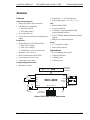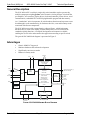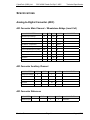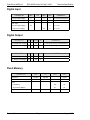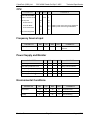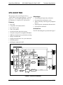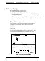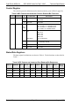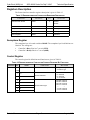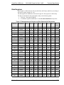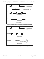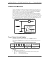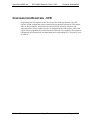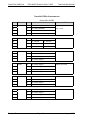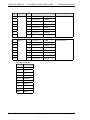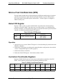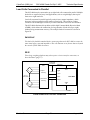
1
SOC-4000/i Scale-On-Chip ASIC Technical Specification August 2002 Document order number: SOC-4000-0001-SP SOC-4000/i Scale-On-Chip ASIC Technical Specification August 2002 Document order number: SOC-4000-0001-SP CybraTech (2000) Ltd. SOC-4000/i Scale-On-Chip ASIC Technical Specification 2002 CybraTech (1998) Ltd. All rights reserved. CybraTech (1998) Ltd. reserves the right to alter the equipment specifications and descriptions in this publication without prior notice. No part of this publication shall be deemed to be part of any contract or warranty unless specifically incorporated by reference into such contract or warranty. The information contained herein is merely descriptive in nature, and does not constitute a binding offer for the sale of the product described herein. CybraTech (2000) Ltd. SOC-4000/i Scale-On-Chip ASIC Technical Specification TABLE OF CONTENTS GENERAL ....................................................................................................................................................1 GENERAL DESCRIPTION ............................................................................................................................2 ADVANTAGES ............................................................................................................................................2 SPECIFICATIONS......................................................................................................................................3 ANALOG-TO-DIGITAL CONVERTER (ADC)...............................................................................................3 A/D Converter Main Channel – Wheatstone Bridge (Load Cell) .........................................................3 A/D Converter Auxiliary Channel.........................................................................................................3 A/D Converter Reference ......................................................................................................................3 DIGITAL INPUT ..........................................................................................................................................4 DIGITAL OUTPUT .......................................................................................................................................4 FLASH MEMORY ........................................................................................................................................4 CPU ...........................................................................................................................................................5 FREQUENCY SOURCE INPUT ......................................................................................................................5 POWER SUPPLY AND MONITOR .................................................................................................................5 ENVIRONMENTAL CONDITIONS .................................................................................................................5 ABSOLUTE MAXIMUM RATING .................................................................................................................6 DIMENSIONS ..............................................................................................................................................6 SCALE MAIN BOARD LAYOUT AND ASSEMBLY PROCESS PARAMETERS FOR SOC-4000........................7 PIN CONFIGURATION .............................................................................................................................9 CPU 80C51TBO .........................................................................................................................................15 MEMORY .................................................................................................................................................16 Organization .......................................................................................................................................16 Program Memory Mapping.................................................................................................................16 Program Memory Bank Select Register ..............................................................................................16 Application Program Start Address ....................................................................................................16 Serial Downloading (In-Circuit Programming)..................................................................................17 Using the Flash for Data Memory ......................................................................................................18 Data Memory Mapping .......................................................................................................................19 CPU SFRs and Configuration Registers (CFRs) ................................................................................20 INSTRUCTION SET ....................................................................................................................................20 RESET ......................................................................................................................................................20 INTERRUPT VECTORS ..............................................................................................................................20 ADC CONTROLLER INTERFACE .......................................................................................................23 CONTROLLER REGISTERS ........................................................................................................................23 Semaphore Register.............................................................................................................................23 Control Register ..................................................................................................................................24 Status/Data Registers ..........................................................................................................................24 Revision B Page i August, 2002 CybraTech (2000) Ltd. SOC-4000/i Scale-On-Chip ASIC Technical Specification OPERATION ..............................................................................................................................................26 KEYBOARD CONTROLLER................................................................................................................. 29 CONTROLLER REGISTERS ........................................................................................................................31 REGISTERS DESCRIPTION.........................................................................................................................31 Control Register ..................................................................................................................................31 Data Registers .....................................................................................................................................31 OPERATION ..............................................................................................................................................32 LED/VFD SERIAL INTERFACE DISPLAY CONTROLLER ........................................................... 35 REGISTERS DESCRIPTION.........................................................................................................................36 Control Register ..................................................................................................................................37 Semaphore Register.............................................................................................................................37 Data Registers .....................................................................................................................................37 OPERATION ..............................................................................................................................................38 PRINTER SERIAL INTERFACE CONTROLLER ............................................................................. 39 REGISTERS DESCRIPTION.........................................................................................................................40 Semaphore Register.............................................................................................................................40 Control Register ..................................................................................................................................40 Data Registers .....................................................................................................................................41 OPERATION ..............................................................................................................................................42 PRINTER HEAD DATA INTERFACE OPERATION .......................................................................................43 STROBE CONTROLLER ....................................................................................................................... 45 REGISTER DESCRIPTION ..........................................................................................................................47 Strobe Clock Enable Control Register ................................................................................................47 Trigger Registers .................................................................................................................................48 Data Registers .....................................................................................................................................48 OPERATION ..............................................................................................................................................50 PRINTER MOTOR AND SENSOR INTERFACE ............................................................................... 51 PRINTER MOTOR OPERATION ..................................................................................................................51 INTERFACING THE PRINTER OPTO-SENSORS ...........................................................................................51 IMPLEMENTING END OF LABEL DETECTOR .............................................................................................53 IMPLEMENTING LABEL PEEL-OFF DETECTOR:.........................................................................................53 CONNECTING THE PRINTER HEAD THERMISTOR TO THE SOC-4000.......................................................54 PROGRAMMABLE FREQUENCY CONTROLLER.......................................................................... 57 CONTROL REGISTERS DESCRIPTION ........................................................................................................58 OPERATION ..............................................................................................................................................58 WATCHDOG TIMER.............................................................................................................................. 59 CONTROL REGISTERS DESCRIPTION ........................................................................................................59 OPERATION ..............................................................................................................................................59 LOW VOLTAGE DETECTOR ............................................................................................................... 61 POWER FAILURE INTERRUPT REGISTER ..................................................................................................61 CONFIGURATION REGISTERS - CFR............................................................................................... 63 Revision B Page ii August, 2002 CybraTech (2000) Ltd. SOC-4000/i Scale-On-Chip ASIC Technical Specification SPECIAL FUNCTION REGISTERS (SFR) ...........................................................................................67 GLOBAL CFR REGISTER..........................................................................................................................67 Operation ............................................................................................................................................67 CONTROLLERS CLOCK ENABLE REGISTERS ............................................................................................67 CONTROLLERS RESET REGISTERS .........................................................................................................69 I/O OPERATION.......................................................................................................................................71 8051-COMPATIBLE ON-CHIP PERIPHERALS..................................................................................73 PARALLEL I/O PORTS ..............................................................................................................................73 Timers/Counters..................................................................................................................................73 SOC-4000 INITIALIZATION ..................................................................................................................75 PERIPHERAL INTERFACE CONNECTIONS ....................................................................................77 LOAD CELL INTERFACE ...........................................................................................................................77 4-Wire and 6-Wire Interfaces..............................................................................................................77 Load Cells Connected in Parallel .......................................................................................................79 Load Cell Impedance ..........................................................................................................................80 SERIAL COMMUNICATION CHANNEL MULTIPLEXER ..............................................................................80 RS-485 Serial Interface Transmit / Receive Control...........................................................................80 KEYBOARD INTERFACE ...........................................................................................................................81 LED/VFD SERIAL DISPLAY INTERFACE .................................................................................................83 EXTERNAL INTERRUPT SOURCES ............................................................................................................83 Using the Vdet input:...........................................................................................................................84 Using Timer0 and Timer1 inputs: .......................................................................................................84 I2C-COMPATIBLE INTERFACE ..................................................................................................................84 POWER SAVING SCHEMES .......................................................................................................................84 IN-CIRCUIT EMULATOR (ICE) SYSTEM...................................................................................................85 GROUNDING AND BOARD LAYOUT RECOMMENDATIONS .......................................................................85 LCD DISPLAY MODULE INTERFACE .......................................................................................................86 Revision B Page iii August, 2002 CybraTech (2000) Ltd. SOC-4000/i Scale-On-Chip ASIC Technical Specification LIST OF FIGURES FIGURE 1: FIGURE 2: FIGURE 3: FIGURE 4: FIGURE 5: FIGURE 6: FIGURE 7: FIGURE 8: FIGURE 9: FIGURE 10: FIGURE 11: FIGURE 12: FIGURE 13: FIGURE 14: FIGURE 15: FIGURE 16: FIGURE 17: FIGURE 18: FIGURE 19: FIGURE 20: FIGURE 21: FIGURE 22: FIGURE 23: FIGURE 24: FIGURE 25: FIGURE 26: FIGURE 27: FIGURE 28: FIGURE 29: FIGURE 30: FIGURE 31: FIGURE 32: Revision B SOC-4000 TYPICAL APPLICATION ........................................................................................ 1 SOC-4000 MAXIMAL BLOCK DIAGRAM ............................................................................... 2 MECHANICAL OUTLINE DRAWING ........................................................................................ 6 PCB BOARD LAYOUT ............................................................................................................ 7 SOC-4000 PIN ARRANGEMENT ........................................................................................... 12 SOC-4000 PIN CONFIGURATION ......................................................................................... 13 CPU BLOCK DIAGRAM ........................................................................................................ 15 SOC-4000/I STARTUP PROCEDURE ..................................................................................... 17 SOC-4000 PROGRAM MEMORY MAP .................................................................................. 18 SOC-4000 DATA MEMORY MAP ......................................................................................... 19 KEYBOARD MATRIX CONFIGURATION ................................................................................ 30 LED/VFD SERIAL INTERFACE DISPLAY BLOCK DIAGRAM ................................................ 35 LED/VFD SERIAL INTERFACE CONTROLLER TIMING DIAGRAM ........................................ 36 PRINTER INTERFACE BLOCK DIAGRAM ............................................................................... 39 SERIAL HEAD TIMING DIAGRAM ......................................................................................... 43 PRINTER STROBE STRETCHER ............................................................................................. 45 AUXILIARY MOTOR (AUXMOTOR) PULSE STRETCHER (PIN 29)...................................... 46 PRINTER POWER (VPP) PULSE STRETCHER (PIN 28)........................................................... 46 PRINTER MOTOR TIMING DIAGRAM .................................................................................... 51 OPTO-SENSOR INTERFACE TO SOC-4000 ............................................................................ 52 END OF LABEL DETECTOR .................................................................................................. 53 PEEL-OFF LABEL DETECTOR (AUTO).................................................................................. 53 EXAMPLE OF RESISTANCE/TEMPERATURE VARIATION FOR THE THERMISTOR ................. 54 THERMISTOR SENSOR .......................................................................................................... 55 CLOCK GENERATOR BLOCK DIAGRAM ............................................................................... 57 LOW VOLTAGE DETECTOR .................................................................................................. 61 4-WIRE LOAD-CELL CONNECTION ...................................................................................... 78 6-WIRE LOAD-CELL CONNECTION ...................................................................................... 78 MULTIPLE LOAD-CELL CONNECTION.................................................................................. 79 KEYBOARD INTERFACE ....................................................................................................... 82 SOC-4000 INTERFACE TO A LED/VFD DISPLAY ................................................................ 83 LCD DISPLAY MODULE HARDWARE INTERFACE ............................................................... 86 Page iv August, 2002 CybraTech (2000) Ltd. SOC-4000/i Scale-On-Chip ASIC Technical Specification LIST OF TABLES TABLE 1: TABLE 2: TABLE 3: TABLE 4: TABLE 5: TABLE 6: TABLE 7: TABLE 8: TABLE 9: TABLE 10: TABLE 11: TABLE 12: TABLE 13: TABLE 14: TABLE 15: TABLE 16: TABLE 17: TABLE 18: TABLE 19: TABLE 20: TABLE 21: TABLE 22: TABLE 23: TABLE 24: TABLE 25: TABLE 26: TABLE 27: TABLE 28: TABLE 29: TABLE 30: TABLE 31: TABLE 32: TABLE 33: TABLE 34: TABLE 35: TABLE 36: TABLE 37: TABLE 38: TABLE 39: TABLE 40: TABLE 41: TABLE 42: Revision B SOC-4000 PIN CONFIGURATION FOR PRINTER ..........................................................................9 INTERRUPT VECTORS DESCRIPTION .........................................................................................21 ADC CONTROLLER REGISTERS DESCRIPTION .........................................................................23 ADC CONTROLLER INTERFACE SEMAPHORE REGISTER BIT DEFINITIONS .............................23 ADC CONTROLLER INTERFACE CONTROL REGISTER BIT FUNCTIONS ....................................24 ADC CONTROLLER INTERFACE DATA REGISTER BIT DEFINITIONS ........................................24 ADC CONTROLLER INTERFACE DATA REGISTER BIT FUNCTIONS ..........................................25 ADC OUTPUT COUNTS VS. ADC SETTINGS ..........................................................................27 KEYBOARD CONTROLLER REGISTERS DESCRIPTION ...............................................................31 KEYBOARD CONTROLLER CONTROL REGISTER BIT FUNCTIONS .........................................31 KEYBOARD CONTROLLER DATA REGISTER BIT DEFINITIONS .............................................32 LED SERIAL CONTROLLER DRIVER REGISTERS DESCRIPTION ............................................36 LED/VFD SERIAL INTERFACE DISPLAY CONTROL REGISTER BIT FUNCTIONS ..................37 LED/VFD SERIAL INTERFACE DISPLAY DATA REGISTER BIT DEFINITIONS.......................38 PRINTER INTERFACE CONTROLLER REGISTERS DESCRIPTION .............................................40 PRINTER INTERFACE CONTROLLER CONTROL REGISTER BIT FUNCTIONS...........................40 PRINTER INTERFACE CONTROLLER DATA REGISTER BIT DEFINITIONS ...............................41 STRETCHER CONTROLLER REGISTERS DESCRIPTION ...........................................................47 STROBE CLOCK ENABLE CONTROL REGISTER BIT FUNCTIONS ...........................................47 TRIGGER REGISTER DEFINITIONS .........................................................................................48 STRETCHER CONTROLLER DATA REGISTER BIT DEFINITIONS ............................................48 STRETCHER RESET REGISTER DEFINITIONS .........................................................................49 PRINTER SENSORS INTERFACE .............................................................................................52 ADC CHANNEL 2 OUTPUT RANGE ........................................................................................55 CLOCK FREQUENCY CONTROL REGISTER BIT SETTINGS .....................................................58 WATCHDOG TIMER OPERATING PARAMETERS ....................................................................59 WATCHDOG TIMER COMMAND SEQUENCE ..........................................................................59 POWER-FAILURE INTERRUPT REGISTER BIT SETTINGS .......................................................61 CFR BIT CONFIGURATION ...................................................................................................64 GLOBAL CFR REGISTER .......................................................................................................67 C200H CLOCK ENABLE REGISTER .......................................................................................67 C200H CONTROLLERS CLOCK ENABLE REGISTER BIT FUNCTIONS ....................................68 C201H CONTROLLERS CLOCK ENABLE REGISTER BIT FUNCTIONS ....................................68 CONTROLLERS RESET REGISTER ........................................................................................69 BIT-ORIENTED I/O PORTS ADDRESSES, PIN AND BIT ASSIGNMENT ....................................71 BYTE-ORIENTED OUTPUT PORTS ADDRESSES AND PIN ASSIGNMENT ................................72 AVAILABLE PINS ON THE 80C51 I/O PORT ..........................................................................73 COMMUNICATION CHANNEL MULTIPLEXER CONTROL .......................................................80 I2C-COMPATIBLE INTERFACE HARDWARE INTERFACE .......................................................84 SOC-4000 INTERFACE SIGNALS TO LCD DISPLAY MODULE ..............................................86 LCD DISPLAY MODULE INTERFACE SIGNALS .....................................................................87 REGISTERS ADDRESSES AND FUNCTION ..............................................................................87 Page v August, 2002 CybraTech (2000) Ltd. Technical Specification SOC-4000/i Scale-On-Chip ASIC GENERAL • Sample Rate – 5, 10, 20 samples/sec • Programmable gain – 0.5, 0.75, 1, 1.5, 2 Features Scale-On-Chip System • Single-Chip Printer Scale electronics • Full OIML R-76 compliance SOC-4000–3000 d SOC-4000i–6000 d • Up to eight load cells • 6-wire load cell connection (including Sense inputs) Peripherals • Display Supports LCD, LED and VFD: LED: Up to 24 digits VFD: Up to 24 digits LCD Module: 4 lines x 20 characters • Keyboard: Up to 128 keys • Serial communication: RS-232/485 • I/O (set-points): Up to 16 lines • Temperature sensor input CPU • Enhanced 80C51TBO • 4 cycles/instruction • 512 KByte, field-programmable Flash program and data memory • Up to 512 KByte SRAM with battery backup support • 4KByte non-volatile Data Flash Power • 5/3.3V operation, 10mA • Power failure detector Applications • • • • Price computing printer scales Weighing indicators Counting scales Checkout scales Analog-to-Digital Converters • Resolution – 20 bits 8 . . . . . 888 Exc+ Tx/Rx Sig+ ExcSig- Load Cell VIN Buzzer LED Module LCD Module VFD Module SOC-4000 Buzzer KB 1-8 KBI 1-16 Keyboard Up to 128 keys x2 Head Sensors Motor VIN I/O (Setpoints) Vcc FIGURE 1:SOC-4000 TYPICAL APPLICATION Revision B Page 1 August, 2002 CybraTech (2000) Ltd. Technical Specification SOC-4000/i Scale-On-Chip ASIC General Description The SOC-4000 ASIC is an 84-pin, single-chip scale intended to replace present-day, multiple-component weighing printer scale electronic circuitry designs. It includes the pre-amplifier, A/D converter, display drivers, keyboard controller, printer drivers, serial communication, embedded CPU and field-programmable program and data memory. As a "stand-alone" unit it incorporates all scale hardware functions and represents a true breakthrough in scale manufacturing. It eliminates the risks, costs and inventory needs associated with discrete components. The SOC-4000 comes with a comprehensive software library, which implements hardware drivers, such as the display, keyboard and printer, as well as most of the standard weighing functions. A complete development environment is available, enabling the user to tailor and customize the application according to specific needs. The general SOC-4000 block diagram is presented in Figure 2. Advantages • • • • Generic OIML R-76 approval Minimize hardware and software development Significantly cuts time-to-market Reduces inventory needs Displays Ref+ Ref- Serial Display Controllers LCD / LED / VFD 20 - 24 Digits Load Cell PGA Delta - Sigma ADC 20 Bits MUX MicroController Core And Peripherals Serial Communication (2) (RS-232 / RS-485) 80C51TBO Printer Head 512K x 8 Program / Data Flash Aux. Channel 512K x 8 RAM Watchdog Timer Printer Controller 3 x 16-Bit Timers Power Supply Monitor VDET Power-Down Detector Printer Motor Printer Sensors I2C Compatible SPI Like Serial Interfaces UART Internal Bandgap Reference Frequency Controller 8 I/O Keyboard Controller 8 x 16 8 Oscillator/ Resonator Keyboard FIGURE 2:SOC-4000 MAXIMAL BLOCK DIAGRAM Revision B Page 2 August, 2002 CybraTech (2000) Ltd. SOC-4000/i Scale-On-Chip ASIC Technical Specification SPECIFICATIONS Analog-to-Digital Converter (ADC) A/D Converter Main Channel – Wheatstone Bridge (Load Cell) PARAMETER MIN Differential Input Voltage Programmable Gain TYP MAX 0 +10 0.5 2 UNIT mV Up to 8 load cell Offset Drift vs. Temperature 20 ppm/ºC Gain Drift vs. Temperature 4 ppm/ºC Integral Non-linearity <0.004 % Common-Mode Rejection (CMR) 120 dB Power Supply Rejection 120 dB Output Noise 200 Sample Rate 5 Of full scale nVp-t-p Resolution 10 COMMENTS 20 bit 20 Samples/s ±1 count A/D Converter Auxiliary Channel PARAMETER MIN Analog Input Voltage 0 TYP MAX UNIT 1 V Offset Drift 20 ppm/ºC Gain Drift 4 ppm/ºC Resolution 20 Bit 20 Samples/s Sample Rate 5 10 COMMENTS A/D Converter Reference PARAMETER Reference Input Revision B MIN TYP MAX UNIT 5 V Page 3 COMMENTS Ratiometric August, 2002 CybraTech (2000) Ltd. Technical Specification SOC-4000/i Scale-On-Chip ASIC Digital Input PARAMETER MIN TYP MAX UNIT COMMENTS VIH (Input High Voltage) 2 5 V TTL Level excluding XTAL VIL (Input Low Voltage) 0.0 0.8 V TTL Level excluding XTAL V VDD = 3.3V V VDD = 3.3V XTAL Input 2.5 VIH (Input High Voltage) 0.4 VIL (Input Low Voltage) Digital Output PARAMETER MIN TYP MAX UNIT COMMENTS VOH (Output High Voltage) 3.3 V TTL Level set by user by external resistors VOL (Output Low Voltage) 0.0 0.8 V TTL Level set by user by external resistors PARAMETER MIN TYP MAX UNIT VOH (Output High Voltage) 3.3 V VOL (Output Low Voltage) 0.0 0.8 V COMMENTS Flash Memory PARAMETER Endurance Data Retention MIN TYP 10,000 100,000 MAX UNIT Cycles 100 Years Erase Full Memory 100 ms Single Block (4kByte) 25 ms 20 us Program Byte Revision B Page 4 August, 2002 CybraTech (2000) Ltd. SOC-4000/i Scale-On-Chip ASIC Technical Specification CPU PARAMETER MIN TYP MAX UNIT COMMENTS Enhanced 80C51TBO RESET Threshold Level 3.98 Start-Up Time V 500 ms • From Power On 1 ms • From Idle Mode • From Power Down 1 500 ms ms 1 ms Oscillator power-down not through OSCEN bit. Oscillator power-down through OSCEN bit. From Watchdog Reset Frequency Source Input PARAMETER MIN TYP MAX UNIT 16 MHz Frequency COMMENTS Crystal oscillator or resonator Power Supply and Monitor PARAMETER MIN Input Voltage Monitor TYP MAX UNIT 4.50 4.75 COMMENTS V Power Fail Input Monitor Level Set by external resistors Analog Voltage Input (AVCC) 4.75 5.00 5.25 V Digital Voltage Input (VCC) 3.00 3.30 3.60 V 15 mA Power Supply Current (IIN) Environmental Conditions PARAMETER Temperature Humidity Revision B MIN TYP MAX UNIT -10 20 40 ºC Full performance -20 20 70 ºC Operating 95 % Non-condensing 0 Page 5 COMMENTS August, 2002 CybraTech (2000) Ltd. Technical Specification SOC-4000/i Scale-On-Chip ASIC Absolute Maximum Rating PARAMETER MIN MAX UNIT AVCC 6 V Analog power VDD 4 V Digital power VCC 6 V Power 5.5 V Input Signal Voltage COMMENTS Operating Temperature –20 +70 ºC Storage Temperature –20 +85 ºC Manual soldering 300 ºC Soldering for 10 seconds Reflow soldering 225 ºC 60 seconds Lead Temperature Dimensions The outline dimensions of the SOC-4000 case is shown in Figure 3. 0.045 X 45º (1.143) PIN 1 Indicates relative locations of Pin 1 1.150 (29.20) Sq. 1.158 (29.41) 1.185 (30.09) Sq. 1.155 (30.35) FIGURE 3:MECHANICAL OUTLINE DRAWING Revision B Page 6 August, 2002 CybraTech (2000) Ltd. SOC-4000/i Scale-On-Chip ASIC Technical Specification Scale Main Board Layout And Assembly Process Parameters For SOC-4000 PCB Layout and Production Guidelines 1. Pad definition will be according to Figure 4. All dimensions are in milli-inches (mil). 2. Solder mask opening should be 3mil (total 6 mil). 3. Board finish may be HAL (hot air leveling), immersion gold over nickel or immersion. Assembly Guidelines 4. Verify that the SOC-4000 components are packaged in hermetically sealed package. If The packaging is damaged or has been removed, perform the following drying procedure to assure that SOC-4000 components are completely dry: • Components drying procedure: Place the SOC-4000 components in their tray and put them into a baking oven to dry at a temperature of 105ºC for a minimum of 6 hours. 5. Reflow temperature profile should be set according to the paste parameters. 6. Maximum reflow temperature should be less than 225 ºC. 7. Recommended paste: Koki, AIM, Multicore Type 3 NC RMA or equivalent. FIGURE 4:PCB BOARD LAYOUT (Dimensions are in milli-inches (mil)) Revision B Page 7 August, 2002 CybraTech (2000) Ltd. Technical Specification SOC-4000/i Scale-On-Chip ASIC PIN CONFIGURATION Glossary of terms regarding SOC-4000 pin configuration are presented on page 12. The physical pin arrangement is shown in Figure 5 and Figure 6, page 12. TABLE 1:SOC-4000 PIN CONFIGURATION FOR PRINTER PIN NAME ND DESCRIPTION 2 FUNCTION 1 KOUT4 2 KOUT3 3 KOUT2 I.O P14.5 4 KOUT1 I.O P14.6 5 KOUT0 I.O P14.7 6 VDD Digital Power Supply, 3.3V 7 KIN7 8 KIN6 Keyboard Controller Input. (See “Keyboard Controller”, page 29) 9 KIN5 I.O P15.2 10 KIN4 I.O P15.3 11 KIN3 I.O P15.4 12 KIN2 I.O P15.5 13 KIN1 I.O P15.6 14 KIN0 I.O P15.7 15 BUZZER 16 SCL Keyboard Controller output. (See “Keyboard Controller”, page 29) Buzzer I.O P14.3 I.O P14.4 I.O P15.0 I.O P15.1 I/O 50k (See “I/O Operation” on page 71) I/O 50k (See “I/O Operation” on page 71) P1.7 (CPU) 25k P1.5 (CPU) 10k 2 P1.4 (CPU) I C Serial Clock SDA I C Serial Data 18 XTAL OUT Frequency source 19 XTAL IN 20 TX 21 RX 22 TX2 OUT P4.0 23 RS485 OUT P4.1 24 RX2 25 LABEL DET. Serial communication 100k Outputs (See “I/O Operation” on page 71) 100K Label detect input. I.O P3.4(CPU) CPU I/O Ports (See page 53) AUTO DET. PULL-UP RESISTOR 2 17 26 DESCRIPTION 50K Or, Prepack label removal detector input. I.O P3.5(CPU) P3.4-TIMER 0 P3.5-TIMER 1 (See page 53) 27 PAPER DET. Paper detect input. I.O P1.6(CPU) (See page 53) Revision B Page 9 August, 2002 CybraTech (2000) Ltd. PIN 28 NAME VPP Technical Specification SOC-4000/i Scale-On-Chip ASIC DESCRIPTION Printer head heater power control. ND 2 FUNCTION OUT P4.2 DESCRIPTION PULL-UP RESISTOR Outputs (See “I/O Operation” on page 71) (See “Strobe Controller”, page 45 and “Printer Head Data Interface Operation”, page 43) 29 AUXMOTOR Auxiliary motor control OUT P4.3 30 MOTOR1 Motor control. OUT P5.0 31 MOTOR2 32 MOTOR3 (See also “Printer Motor Operation” OUT P5.1 page 51) OUT P5.2 33 MOTOR4 OUT P6.0 34 MOTOR5 OUT P6.1 35 MOTOR6 OUT P6.2 36 STROBE1/OE1 Printer head dot control OUT P6.3 37 STROBE2/OE2 (See “Strobe Controller”, page 45) OUT P7.0 Outputs 38 STROBE3/OE3 OUT P7.1 39 STROBE4/OE4 OUT P7.2 (See “I/O Operation” on page 71) 40 STROBE5/OE5 OUT P7.3 41 STROBE6/OE6 OUT P8.0 42 SWITCH Printer head switch detector input I.O P18.0 I/O 50k (See “I/O Operation” on page 71) 43 PRN LATCH 44 45 PRN_SI_DATA (See “Printer Serial Interface Controller”, page 39 and “Printer PRN_SI_CLK Head Data Interface Operation”, page 43) 46 D0 OUTPUT 47 D1 OUTPUT 48 D2 OUTPUT 49 D3 OUTPUT 50 D4 OUTPUT 51 D5 OUTPUT 52 D6 OUTPUT 53 D7 OUTPUT 54 RDLCD (A1) Read Signal for LCD display module. (See page 86) OUT P12.0 Output 55 WRLCD (A0) Write Signal for LCD display module. (See page 86) OUT P12.1 (See “I/O Operation” on page 71) 56 CSLCD Chip Select for LCD display module. (See page 86) OUT P12.2 57 VBAT RAM backup voltage input Revision B Printer serial data interface. OUT P8.1 Outputs OUT P8.2 (See “I/O Operation” on page 71) OUT P8.3 LCD Display module interface, data bus interface. Output only. (See “LCD Display Module Interface”, page 86) Page 10 August, 2002 CybraTech (2000) Ltd. PIN NAME SOC-4000/i Scale-On-Chip ASIC DESCRIPTION LED/VFD Serial Interface Display Module Clock, Data, Strobe and Blank. (See “LED/VFD Serial Display Controller”, page 47) ND 2 FUNCTION 58 LED_SI_CLK 59 LED_SI_Data 60 LED_SI_ST 61 LED_SI_BL 62 VCC Power Supply 63 RESET Reset 64 GND Digital Ground 65 VDET/INT0~ Power voltage detector input / Interrupt0 Input 66 SIG2+ 2nd channel input signal + 67 SIG2– 2nd channel input signal – 68 AGND Analog Ground 69 SEN– Load cell Sense input – 70 SIG1– Load cell signal input – 71 SIG1+ Load cell signal input + 72 SEN+ Load cell Sense input + 73 AVCC Analog power supply 74 KIN15 75 KIN14 Keyboard Controller input. (See “Keyboard Controller”, page 29) 76 KIN13 I.O 17.2 77 KIN12 I.O 17.3 78 KIN11 I.O 17.4 79 KIN10 I.O 17.5 80 KIN9 I.O 17.6 81 KIN8 I.O 17.7 82 KOUT7 83 KOUT6 84 KOUT5 Revision B OUT 13.0 OUT 13.1 Technical Specification DESCRIPTION PULL-UP RESISTOR Output (See “I/O Operation” on page 71) OUT 13.2 OUT 13.3 50k Keyboard Controller Output. (See “Keyboard Controller”, page 29) I.O 17.0 I.O 17.1 I/O 50k (See “I/O Operation” on page 71) I.O 14.0 I.O 14.1 I.O 14.2 Page 11 August, 2002 CybraTech (2000) Ltd. SOC-4000/i Scale-On-Chip ASIC Technical Specification Glossary of Terms TERM DEFINITION ST Schmidt-Trigger 3-ST Tri-State I Input O Output I.O Input/Output PRN Printer SI Serial Interface CLK Clock RD Read WR Write KIN Keyboard Input KOUT Keyboard Output Pxx.x I/O Port FIGURE 5:SOC-4000 PIN ARRANGEMENT Revision B Page 12 August, 2002 CybraTech (2000) Ltd. SOC-4000/i Scale-On-Chip ASIC Technical Specification FIGURE 6:SOC-4000 PIN CONFIGURATION Revision B Page 13 August, 2002 CybraTech (2000) Ltd. Technical Specification SOC-4000/i Scale-On-Chip ASIC CPU 80C51TBO The reference source for data given here is “M8051TBO Technical Specifications”, Virtual IP Group, Inc., Version M8051TS97DF02. Refer to this manual for a complete CPU specification. Advantages • Fast running and improved performance • No wasted clock and memory cycles • Works efficiently with all types of peripheral devices • Improved power consumption characteristics • On-chip Power-On/Reset Features Architecture PSW ALU Reg. 2 ALU Stack Pointer Interrupt Logic DPTR1 SFR RAM Address Timer 0 256 Bytes SFR 8 RAM Port Latch DPTR0 Power Control Register Data Bus PS EN Clocks and Memory Control PC Increment Program Counter Interrupt Reg. Instruction Decoder ALE XTAL 2 RST Oscillator XTAL 1 Reset Control Address Bus Buffer Timed Access Timer 1 Serial Port 0 Port Latch Port 3 PC Address Reg. P3.0 to P3.7 AD0 to AD7 B Register ALU Reg. 1 P2.0 to P2.7 Accumulator Port 0 The CPU block diagram is presented in Figure 7. Port 2 Timer 2 Port 1 Port Latch 8-bit CPU Compatible with standard 80C31 Four 8-bit I/O ports Three 16-bit timers On-chip oscillator and clock circuitry 256-byte on-chip, 8051-compatible SFR RAM 64Kbyte program memory with bank switching 4Kbyte external RAM High-speed architecture of 4 cycles/instruction Dual data pointers Full-Duplex enhanced UART P1.0 to P1.7 • • • • • • • • • • • FIGURE 7:CPU BLOCK DIAGRAM Revision B Page 15 August, 2002 CybraTech (2000) Ltd. SOC-4000/i Scale-On-Chip ASIC Technical Specification Memory Organization The SOC-4000 is an 8051-compatible device with an 80C310 memory chip. As with all such devices, the SOC-4000 has separate address spaces for Program and Data memory. The program memory space can be programmed while the device is in circuit through the serial port. • Flash memory – memory space containing non-volatile, in-circuit re-programmable code and data (such as calibration data). The code in the Flash memory may be in-circuit programmed at a byte level, although it must first be erased, the erasing being performed in page blocks. The program memory space can be in-circuit programmed through the serial port. • RAM memory – Temporary memory used as “scratchpad memory” for the software. Program Memory Mapping The 8051-compatible SOC-4000 supports a maximum code space of 64K. Programs larger than 64K are handled by bank switching, in order to select one of a number of code banks residing at one physical address. In the SOC-4000, there is one 32K Common-Program Area mapped from address 1000H to 7FFFH (Figure 9) and 15 x 32K code banks mapped from code address 8000H to FFFFH (Figure 9). The code banks are selected using P1.0 to P1.3, as described below. Program Memory Bank Select Register The program memory bank select register is implemented using the 80C51TBO Port 1 bits P1.0 – P1.3. P1.0 is the least significant bit. Manipulation of other Port 1 I/O pins must be carried out without affecting these bits. To enable the program memory access set registers C104H, C105H and C106H to AAH as follows: C104H = AAH C015H = AAH C106H = AAH NOTE: The page register is WRITE ONLY! Reading P1.0-P1.3 may result in an ambiguous result. Application Program Start Address The start address of the application program should be located at 1000H, as the first 4kBytes are reserved for the SOC-4000/I system. Revision B Page 16 August, 2002 CybraTech (2000) Ltd. Technical Specification SOC-4000/i Scale-On-Chip ASIC Serial Downloading (In-Circuit Programming) As part of its embedded boot software, the SOC-4000 facilitates serial code and data download via the standard UART serial port. Serial download mode is automatically entered upon power-up or reset if one of the following conditions exists • No valid program is programmed in the Flash memory. • A request for download process was initiated via the UART during the first 200 ms after power-up/reset. Once in this mode, you can download code or data files into the Flash memory, while the device is located in its target board. The CybraTech Cloader executable is the PC serial download utility provided together with the device and its documentation and software library. The SOC-4000/I may be programmed only if within 200ms after power-up or RESET it established communication with the Cloader executable, or if the application program is not available or not valid (checksum error). Figure 8 describe the startup procedure of the SOC4000. Power-Up / Reset Start Programming mode Yes Is Cloader Communicating ? No 200 ms elapsed ? No Yes No Is the Application Program OK? Yes Start Application Program FIGURE 8:SOC-4000/I STARTUP PROCEDURE Revision B Page 17 August, 2002 CybraTech (2000) Ltd. SOC-4000/i Scale-On-Chip ASIC Technical Specification Using the Flash for Data Memory The Flash memory may be used for storing non-volatile data. To update the data area while the program is running,the Flash must be defined as a DATA area (and not as a CODE area). CybraTech Flash Manager software manages this process in an efficient and reliable manner. It provides the means to read, write, erase and update the Flash Data area. A detailed description of the CybraTech Flash Manager function is included in the SOC-4000 Software Function Library user manual, document number: SOC-0000-SW01-OM. FFFFH Program Bank 1 32K Program Bank 2 32K F800H ......... Flash Data Memory Program Bank 15 32K 8000H 7FFFH 1000H FFFH 0000H Program Common Area 32K Bank 0 4K Reserved by System FIGURE 9:SOC-4000 PROGRAM MEMORY MAP Revision B Page 18 August, 2002 CybraTech (2000) Ltd. SOC-4000/i Scale-On-Chip ASIC Technical Specification Data Memory Mapping The SOC-4000 data memory is stored in 3 areas: a. 256-bytes internal RAM, mapped as IDATA. b. 4kByte RAM located at addresses 8000H – 8FFFH. This memory is mapped as XDATA memory and is used as the SOC-4000 working RAM and scratchpad memory. c. Up to 512kByte RAM with battery backup mapped at address range 0000H – 7FFFH as XDATA memory mapped as 16 page of 32kByte each. This area may be used as data area to store transactions, PLUs and any other non-volatile data required by the application. RAM Bank Select Register CFR C113H (bits 0-3) is the page register controlling the active RAM page. To enable the C113H register set C104H, C105H and C106H to AAH C104H = AAH C015H = AAH C106H = AAH For SOC-4000 with 128kByte RAM only bits 0-1 are applicable (bit 0 – LSB). For SOC-4000 with 512kByte RAM bits 0-3 are applicable (bit 0 – LSB). FIGURE 10:SOC-4000 DATA MEMORY MAP Revision B Page 19 August, 2002 CybraTech (2000) Ltd. SOC-4000/i Scale-On-Chip ASIC Technical Specification CPU SFRs and Configuration Registers (CFRs) The CPU SFRs (Special Function Registers) are compatible with the 8051 instruction set. Please refer to “M8051TBO Technical Specifications”. The CPU controls the peripherals and their operating modes through Configuration Registers (CFRs). The CFR registers for each peripheral are described in Table 29 (page 64). Instruction Set All instructions in the 8051-compatible SOC-4000 instruction set perform the same functions as in the 8051. They identically oversee bit and flag operations and other status functions. Only the clock configuration differs. For absolute timing of real time events, the timing of software loops can be calculated. However, counter/timers default to run at the older 12 clocks per increment. In this way, timer-based events occur at the standard intervals with software executing at higher speed. Timers optionally can run at 4 clocks per increment to take advantage of faster processor operation. In the SOC-4000, the MOVX instruction may take only two machine cycles or eight oscillator cycles, while the “MOV direct, direct” instruction uses three machine cycles or 12 oscillator cycles. Thus, the execution times of the two instructions differ. This is because the SOC-4000 usually uses one instruction cycle for each instruction byte. Note that a machine cycle requires just four clocks, and provides one ALE pulse per cycle. Many instructions require only one cycle, but some require five. Reset The Reset signal is generated by an internal circuit in the ASIC. The signal thresholds are: • RESET falling edge on Vcc = 3.98v • RESET rising edge on Vcc = 4.19v The hystheresis of the Reset signal is set so that normal operation of the internal Flash memory is guaranteed. Interrupt Vectors The interrupt vectors of the SOC-4000/I are shifted compared with the interrupt vectors of a standard 80C51TBO vectors by an offset of 1000H. Table 2 details the SOC-4000/I interrupt vectors: Revision B Page 20 August, 2002 CybraTech (2000) Ltd. SOC-4000/i Scale-On-Chip ASIC Technical Specification TABLE 2:INTERRUPT VECTORS DESCRIPTION INTERRUPT SOURCE FLAG VECTOR LOCATION PRIORITY External Interrupt 0 IE0 1003H 1 (Highest) Timer 0 Overflow TF0 100BH 2 External Interrupt 1 IE1 1013H 3 Timer 1 Overflow TF1 101BH 4 RI + TI 1023H 5 TF2 + EXF2 102BH 6 Serial Port Timer 2 Overflow Revision B Page 21 August, 2002 CybraTech (2000) Ltd. Technical Specification SOC-4000/i Scale-On-Chip ASIC ADC CONTROLLER INTERFACE Features • Resolution – 20 bit • Programmable gain –0.5, 0.75, 1, 1.5, 2 • Programmable sample rate of 5, 10 or 20 samples per second • Voltage detection input and alarm Controller Registers ADC Converter (ADC) controller interface includes a semaphore register (one byte), a control register (two bytes) and a data/status register (four bytes). The ADC controller registers are defined in Table 3. TABLE 3:ADC CONTROLLER REGISTERS DESCRIPTION FUNCTION Controller Clock Enable ADDRESS C200H BIT 7 REMARKS 0 =Disable 1 = Enable Controller RESET C406H All 0xFF = Reset Semaphore Register E100H 0-1 Read/Write Data Registers E103H to E106H All Read only Control Register E101H to E102H All Write only Semaphore Register The semaphore register bit definitions are shown in Table 4. TABLE 4:ADC CONTROLLER INTERFACE SEMAPHORE REGISTER BIT DEFINITIONS ADDRESS E100H Revision B BIT 7 … BIT 2 Don’t Care BIT 1 BIT 0 (LSB) Tx Semaphore Rx Semaphore (Controller to ADC Converter) (ADC Converter to Controller) Page 23 August, 2002 CybraTech (2000) Ltd. Technical Specification SOC-4000/i Scale-On-Chip ASIC Control Register The control register bit definitions and its functions and are given in Table 5 (page 24). TABLE 5:ADC CONTROLLER INTERFACE CONTROL REGISTER BIT FUNCTIONS BYTE # ADDRESS 1 BIT E101H 2 FUNCTION SETTINGS 0 = Disable 1 = Enable 0 Interrupt Enable (LSB) E102H 1-7 Don’t Care Don’t Care 0-1 Sample Rate 00 = 20 Hz (default) & F.S=100,000 Counts 01 = 10 Hz & F.S. = 200,000 Counts 10 = 10 Hz& F.S. = 100,000 Counts 11 = 5 Hz& F.S. = 200,000 Counts Gain 000 = 0.50 001 = 0.75 010 = 1.00 011 = 1.50 100 = 2.00 Power Down 111 = Power Down 5 ADC Channel 0 = Main (default) channel 1 = Secondary channel 6 Don’t Care Don’t Care 7 Don’t Care Don’t Care (bit 0 – LSB) 2-4 Status/Data Registers The data register bit definitions are shown in Table 6. The bit functions are described in Table 7. TABLE 6:ADC CONTROLLER INTERFACE DATA REGISTER BIT DEFINITIONS BYTE # ADDRESS BIT 7 BIT 6 BIT 5 BIT 4 BIT 3 BIT 2 BIT 1 BIT 0 (LSB) 1 E103H D7 D6 D5 D4 D3 D2 D1 D0 2 E104H D15 D14 D13 D12 D11 D10 D9 D8 3 E105H SR1 SR0 D19 D18 D17 D16 4 E106H 0 0 0 0 CH G2/PD2 Revision B G1/PD1 G0/PD0 0 0 Page 24 August, 2002 CybraTech (2000) Ltd. SOC-4000/i Scale-On-Chip ASIC Technical Specification TABLE 7:ADC CONTROLLER INTERFACE DATA REGISTER BIT FUNCTIONS BIT FUNCTION Di ADC Reading Data D0 = LSB D19 = MSB SRi Sample Rate Gi/PDi Gain/Power Down CH Active ADC Channel Revision B Page 25 August, 2002 CybraTech (2000) Ltd. SOC-4000/i Scale-On-Chip ASIC Technical Specification Operation Initialization: To enable the ADC controller interface: 1. Enable the ADC controller interface clock source in Clock Enable register C200H: Set C200H, Bit 7 to 1. 2. Reset the ADC controller interface: Write FF to register C406H. 3. Set the Configuration registers (CFR) address for ADC controller interface function: CFR address C10CH = 1FH. 4. Enable interrupt: Set E101H, Bit 0 to 1. 5. Check the semaphore byte at address E100H. If Receive semaphore bit at E100H is Ready (Bit 0 = 0), signaling the CPU that the ADC controller can receive data, the CPU performs the following operations: a. Sets the Transmit semaphore bit at E100H to Busy (Bit 1 = 1) to prevent transmission of data from the ADC controller. b. Programs the control register E101–E102H of the ADC controller to initialize controller operation. Normal operation: 6. After the ADC controller has been initialized, the following operations are performed: c. The CPU resets the Transmit semaphore bit at E100H to Ready (Bit 1 = 0) to signal the ADC controller that it can now transmit data. d. The ADC controller sets the Receive semaphore bit at E100H to Busy (Bit 0 = 1) to prevent further data transmission to the controller. e. The ADC controller sends ADC converter data to data registers at E103H to E106H. 7. After sending the data of registers E103H to E106H, the ADC controller resets the Receive semaphore bit at E100H to Ready (Bit 0 = 0), signaling the CPU that the controller can now receive new data. One ADC controller operation cycle is now complete. Steps 6 through 7 are repeated cyclically. The ADC internal counts output is dependent upon the input signal, the gain and the operation mode setting. Table 5 defines the relation between the internal counts output of the zero signal input of the full-scale signal and the ADC settings. Revision B Page 26 August, 2002 CybraTech (2000) Ltd. Technical Specification SOC-4000/i Scale-On-Chip ASIC TABLE 8:ADC OUTPUT COUNTS VS. ADC SETTINGS GAIN SAMPLE RATE * ADC RESOLUTION MODE * ADC OUTPUT AT ZERO SIGNAL INPUT MAXIMUM FULL-SCALE INPUT (IN COUNTS) (COUNTS) (MILLI-VOLTS) 20 103,000 153,200 20 256,200 10 103,000 153,200 20 256,200 10 206,000 306,400 20 512,400 5 206,000 306,400 20 512,400 20 103,000 153,200 15 256,200 10 103,000 153,200 15 256,200 10 206,000 306,400 15 512,400 5 206,000 306,400 10 512,400 20 103,000 153,200 10 256,200 10 103,000 153,200 10 256,200 10 206,000 306,400 10 512,400 5 206,000 306,400 10 512,400 20 103,000 153,200 6.6 256,200 10 103,000 153,200 6.6 256,200 10 206,000 306,400 6.6 512,400 5 206,000 306,400 6.6 512,400 20 103,000 153,200 5 256,200 10 103,000 153,200 5 256,200 10 206,000 306,400 5 512,400 5 206,000 306,400 5 512,400 (HZ) 0.5 0.75 1.0 1.5 2.0 ADC OUTPUT (COUNTS) * ADC Resolution mode is defined in Table 5, Register E102H, bits 0-1 – Sample Rate. Revision B Page 27 August, 2002 CybraTech (2000) Ltd. SOC-4000/i Scale-On-Chip ASIC Technical Specification KEYBOARD CONTROLLER Features Functional Description • Supports up to 128 keys (8×16) • Programmable anti-bounce mechanism (4-18 ms) • Automatic key matrix scanning • Automatically detects excessively long or constant key depression • When Interrupt mode enabled, generates an interrupt when any key is pressed or released Keyboard Controller Matrix Configuration Revision B The keyboard matrix configuration showing the 8 × 16 matrix is given in Figure 11. The key code values at each junction are in hexadecimal. Page 29 August, 2002 CybraTech (2000) Ltd. Technical Specification SOC-4000/i Scale-On-Chip ASIC KIN 0 KIN 1 KIN 2 KIN 3 KIN 4 KIN 5 KIN 6 KIN 7 KIN 8 KIN 9 KIN10 K I N 11 KIN12 KIN13 KIN14 KIN15 KOUT 0 * 00 01 02 03 04 05 06 07 08 09 0A 0B 0C 0D 0E 0F KOUT 1 10 11 12 13 14 15 16 17 18 19 1A 1B 1C 1D 1E 1F KOUT 2 20 21 22 23 24 25 26 27 28 29 2A 2B 2C 2D 2E 2F KOUT 3 30 31 32 33 34 35 36 37 38 39 3A 3B 3C 3D 3E 3F KOUT 4 40 41 42 43 44 45 46 47 48 49 4A 4B 4C 4D 4E 4F KOUT 5 50 51 52 53 54 55 56 57 58 59 5A 5B 5C 5D 5E 5F KOUT 6 60 61 62 63 64 65 66 67 68 69 6A 6B 6C 6D 6E 6F KOUT 7 70 71 72 73 74 75 76 77 78 79 7A 7B 7C 7D 7E 7F *Key values are in hexadecimal. FIGURE 11:KEYBOARD MATRIX CONFIGURATION Revision B Page 30 August, 2002 CybraTech (2000) Ltd. SOC-4000/i Scale-On-Chip ASIC Technical Specification Controller Registers Keyboard controller interface includes a control register (one byte) and a data/status register (two bytes). The Keyboard controller registers are defined in Table 9. TABLE 9:KEYBOARD CONTROLLER REGISTERS DESCRIPTION FUNCTION ADDRESS BIT C200H Controller Clock Enable 2 REMARKS 0= Disable 1= Enable Controller RESET C400H All 0xFF = Reset Data Registers F100H to F101H All Read only Control Register F100H All Write only Registers Description Control Register The keyboard control register bit definitions, functions and settings are displayed in Table 10. TABLE 10:KEYBOARD CONTROLLER CONTROL REGISTER BIT FUNCTIONS ADDRESS BIT F100H 0-2 FUNCTION Anti-Bounce Timeout SETTINGS 000 = 4 ms 001 = 6 ms (0-LSB) 010 = 8 ms 011 = 10 ms 100 = 12 ms 101 = 14 ms 110 = 16 ms 111 = 18 ms 3 4-7 Interrupt Enable/Disable 0 = Enable 1 = Disable (default) Don’t Care Don’t Care Data Registers Keyboard data is stored in two 8-bit registers. The data register bit definitions are shown in Table 11 Revision B Page 31 August, 2002 CybraTech (2000) Ltd. SOC-4000/i Scale-On-Chip ASIC Technical Specification NOTE: When Control Register Address F101H, bit 7 is set to 1 (Released), key-code value bits 0 to 6 in address F101H are meaningless. TABLE 11:KEYBOARD CONTROLLER DATA REGISTER BIT DEFINITIONS BYTE # ADDRESS BIT 7 BIT 6 BIT 5 BIT 4 BIT 3 BIT 2 BIT 1 BIT 0 (LSB) 1 F100H 2 F101H X Release Sign 0 = Pressed 1 = Released X X X X X X D6* D5* D4* D3* D2* D1* Key Error Flag 0 = Legal 1 = Error D0* * Key Code Operation At power on, the keyboard controller is reset and the scanning rate is set to 10 µs. Initialization: To enable the keyboard controller: 1. Enable the keyboard controller clock source in Clock Enable register C200H: Set C200H, Bit 2 to 1. 2. Reset the keyboard controller: Write FF to register C400H. 3. Check CFR address for keyboard controller function: CFR addresses C10DH, C10EH, C10FH = FFH (Table 29, page 64). This results in the following operations: • Enables keyboard output pins (1 to 5 and 82 to 84) (Table 29; page 64; Table 1, page 9) • Enables keyboard input pins (7 to 14 and 74 to 81) (Table 29; page 64, Table 1, page 9) NOTE: If less than 128 keys are required, some of the pins may be allocated for I/O operation. See .Table 29:CFR Bit Configuration (page 64) and I/O Operation (page 71). 4. Enable keyboard interrupt: Set F100H, Bit 3 to 0. 5. Set anti-bounce timeout: Set F100H, Bits 0, 1 and 2, as shown in Table 10. Revision B Page 32 August, 2002 CybraTech (2000) Ltd. SOC-4000/i Scale-On-Chip ASIC Technical Specification Normal Operation: 6. Read keyboard key-code value bits, as follows: • Read register F100H, Bit 0: If 0, key-code value is legal. If 1, key-code value is illegal (Error). • Read keyboard values from register F101H, bits 0 to 6: When key pressed, values are valid. • Read F101H, bit 7: If 0, key pressed and keyboard values (bits 0 to 6) are valid. If 1, key released and keyboard values are meaningless. Revision B Page 33 August, 2002 CybraTech (2000) Ltd. Technical Specification SOC-4000/i Scale-On-Chip ASIC LED/VFD SERIAL INTERFACE DISPLAY CONTROLLER Features Functional Description • • • • • The LED/VFD Serial Interface display comprises three groups of eight digits. The controller diagram showing the division of the 24-byte register into three eight-byte groups and the operation cycle is given in Figure 12. Supports up to 24 digits Serial interface Programmable control-signal polarity Programmable data registers Supports common-anode, seven-segment LED Group 1 Seg a Seg b Seg c Seg d Seg e Seg f Seg g DP f Digit 7 Digit 6 Digit 5 a a a b Digit 8 Digit 7 Digit 6 Digit 5 a a a e e c DP d Digit 8 Digit 7 Digit 6 Digit 5 a a a b e b f e c Cycle 1 0 0 0 Cycle 8 1 0 0 0 0 0 0 1 X X X 0 0 0 X X X Digit 1 0 0 X X X X X X X X X X X X X X Group 1 X X X X e c c DP d DP d Digit 3 Digit 2 Digit 1 a a b f e c g e c DP b f g c DP d X X X X X X X X X X X X Group 2 X g a d X b f g e g DP d b f DP e c DP d Digit 1 b f g e c DP d b f g e c DP d b f g e c DP d b f g DP a c a c d Digit 2 d Digit 4 DP a g DP d e c d Digit 3 e c DP d a g e c DP d g a b f g e b f g DP d b f b f c DP a g Digit 1 a e c d Digit 2 a g Digit 4 b f g e c DP b f g e c d f b f e Digit 3 a b f g DP d a g b f c DP d a g e c DP d Digit 4 b f g e c DP b f g e c b f b f g d Group 3 Seg a Seg b Seg c Seg d Seg e Seg f Seg g DP Digit 8 a e Group 2 Seg a Seg b Seg c Seg d Seg e Seg f Seg g DP The LED/VFD Serial Interface Display Controller timing diagram is shown in Figure 13. The clock rate is 2 MHz. X DP d X X X X X X X Group 3 X X The controller transmits cycles 1 to 8 continuously. FIGURE 12:LED/VFD SERIAL INTERFACE DISPLAY BLOCK DIAGRAM Revision B Page 35 August, 2002 CybraTech (2000) Ltd. SOC-4000/i Scale-On-Chip ASIC Technical Specification 20 µs BLANK/ BLANK 20 µs t = 400 µs STROBE/ STROBE 20 µs t1 = 8 µs CLOCK/ CLOCK DATA FIGURE 13:LED/VFD SERIAL INTERFACE CONTROLLER TIMING DIAGRAM Registers Description The LED Serial controller registers description is given in Table 12. TABLE 12:LED SERIAL CONTROLLER DRIVER REGISTERS DESCRIPTION FUNCTION ADDRESS BIT REMARKS Controller Clock Enable C200H 5 Enable/Disable controller Controller RESET C403H All 0xFF = Reset Semaphore register D201H Read only Group 1 D201H to D208H Write Only Group 2 D209H to D210H Write Only Group 3 D211H to D218H Write Only Control Register D200H Read/Write Data Registers LED data is stored in a 24-byte × 8-bit static display RAM. The data registers are divided into three groups, each group containing eight bytes with the segment data for eight digits. Thus, the LED display can be formatted to display eight, 16 or 24 digits. The display RAM has one Read/Write control register containing the Command byte and a Read-only semaphore byte that informs the system if the display is Busy or Ready to initiate writing of LED data. The semaphore byte address also serves as first address of the Write-only data register. The trigger for sending the data out to the display serial interface is programming the control register at address D200H. As soon as the controller starts to send data, it sets the semaphore byte to FFH, indicating that it is busy. When the controller has finished data output, it resets the semaphore byte to 0, indicating that it is available for a new operation. Revision B Page 36 August, 2002 CybraTech (2000) Ltd. SOC-4000/i Scale-On-Chip ASIC Technical Specification Control Register The definitions and functions of the control-register Command-byte bits are displayed in Table 13. TABLE 13:LED/VFD SERIAL INTERFACE DISPLAY CONTROL REGISTER BIT FUNCTIONS ADDRESS BIT D200H 0 NAME C FUNCTION Command bit SETTINGS 0 = Command Only 1 = Command + Data (LSB) 1 X N/A Don’t Care 2 Blank Polarity Sets the Blank polarity. 0 = Negative Logic 1 = Positive Logic 3 Strobe Polarity Sets the Strobe polarity. 0 = Negative Logic 1 = Positive Logic 4 Clock Polarity Sets the Clock polarity. 0 = Negative Logic 1 = Positive Logic 5 E Enables and disables the display. 0 = Disable Display 1 = Enable Display 6 Block 0 = Close communication Opens communication or blocks the hardware communication lines. 1 = Open communication 7 N/A N/A Don’t Care Semaphore Register The semaphore byte is located at address D201H, which is the first address of the Write-only data register. This address is Read-only for the semaphore byte. The semaphore byte bit definitions are identical. The settings are: • Controller is Busy: Bits 0 to 7 set to 1 (FFH). • Controller is Ready: Bits 0 to 7 set to 0 (00H). Data Registers The display data is stored in a 24-byte × 8-bit XDATA area. The data register bit definitions for a 21-digit display are shown in Table 14. The registers are Write-only. Revision B Page 37 August, 2002 CybraTech (2000) Ltd. Technical Specification SOC-4000/i Scale-On-Chip ASIC TABLE 14:LED/VFD SERIAL INTERFACE DISPLAY DATA REGISTER BIT DEFINITIONS GROUP BYTE # ADDRESS BIT 7 # 1 BIT 6 BIT 5 BIT 4 BIT 3 BIT 2 BIT 1 BIT 0 (LSB) 1 D201H DP g f e d c b a 2 D202H DP g f e d c b a 3 D203H DP g f e d c b a 4 D204H DP g f e d c b a 5 D205H DP g f e d c b a 6 D206H DP g f e d c b a 7 D207H DP g f e d c b a 8 D208H DP g f e d c b a 2 9 to 16 D209H to D210H DP g f e d c b a 3 17 to 24 D211H to D218H DP g f e d c b a Operation At power-on or reset the LED/VFD Serial Interface display controller is disabled. Initialization: To enable the LED/VFD Serial Interface display controller: 1. Enable the controller clock source in Clock Enable register C200H: Set C200H, Bit 5 to 1. 2. Reset the controller: Write FF to register C403H. 3. Check CFR address for LED/VFD Serial Interface display controller function: CFR address C101H = AA (Table 29, on page 64). This results in the following operations: Enables serial controller output pins (58 to 61) (Table 29, on page 64). Normal Operation: 4. Check semaphore byte at address D201H. If semaphore byte is Ready (Bits 0 to 7 set to 0), write data to Data register addresses D201H to D218H. 5. Set Write command at the controller Control register address D200H. Repeat steps 4 and 5 for new data. Revision B Page 38 August, 2002 CybraTech (2000) Ltd. SOC-4000/i Scale-On-Chip ASIC Technical Specification PRINTER SERIAL INTERFACE CONTROLLER Features Functional Description • • • • • • The printer head is supported by the serial data and serial clock (pins 44/45). The frequency of the clock can be changed. The dot printer energy may be controlled by up to six strobe lines (STROBE1 – STROBE6). Printer motor and sensors support – see “Strobe Controller” (page 45) and “Interfacing the Printer Opto-Sensors” (page 51). Supports paper and labels. Up to 448 Dots/line. Up to 100 mm/s printing speed. Power voltage failure protection. Auxiliary motor controller (rewinder). Head temperature sensor reading support using ADC 2nd channel. NOTE: The strobe lines also referred to as “Output Enabled (OE)” or “Stretcher lines (STR)”. Power VPP(Pin28) Vch Line of resistors dots (Pin 36) .. .. (Pin 41) 1 448 Dots Strobe 1 (OE1) Strobe 6 (OE6) (Pin 43) PRN Latch Up to 448 bits buffer registers (Pin 44) PRN SI Data Up to 448 bits shift registers (Pin 45) PRN SI Clock FIGURE 14:PRINTER INTERFACE BLOCK DIAGRAM Revision B Page 39 August, 2002 CybraTech (2000) Ltd. SOC-4000/i Scale-On-Chip ASIC Technical Specification Registers Description The Printer interface controller registers description is given in Table 15. TABLE 15:PRINTER INTERFACE CONTROLLER REGISTERS DESCRIPTION COMMAND Controller Clock Enable ADDRESS BIT C200H 6 FUNCTION 0-Disable 1-Enable Controller Reset C405H OxFF=Reset Semaphore Register D801H Data Registers D801H to D838H Write Only Control Register D800H Read/Write All Read only Semaphore Register The semaphore byte is located at address D801H. The semaphore byte bit definitions are identical. The settings are: • Controller is Busy: Bits 0 to 7 set to 1 (FFH). • Controller is Ready: Bits 0 to 7 set to 0 (00H). Control Register The control register bit definitions and functions are given in Table 16. TABLE 16:PRINTER INTERFACE CONTROLLER CONTROL REGISTER BIT FUNCTIONS ADDRESS BIT D800H 0 NAME CLK FUNCTION Sets the Clock Polarity (LSB) 1 Revision B T1 3 L0 4 L1 5 L2 6 L3 7 L4 0 = Negative Logic 1 = Positive Logic Sets the Data Rate 0 0 = 1 MHz 0 1 = 500 KHz 1 0 = 250 KHz 1 1 = 31.75 KHz Sets the Data Length 0 0 0 0 0 = 200 bits 0 0 0 0 1 = 208 bits 0 0 0 1 0 = 216 bits 0 0 0 1 1 = 224 bits … … 1 1 1 1 0 = 440 bits 1 1 1 1 1 = 448 bits T0 2 SETTINGS Page 40 August, 2002 CybraTech (2000) Ltd. SOC-4000/i Scale-On-Chip ASIC Technical Specification Data Registers Data length is variable between 25 bytes (200 bits) and 56 bytes (448 bits), according to the control register setting (L0 – L4). The data register bit definitions are shown in Figure 28. The registers are Write-only. The data is transmitted to the printer head serially, in the following order: a. First byte – data register D801H. b. In each data register the MSB (Bit 7) is the first bit transmitted to the printer. TABLE 17:PRINTER INTERFACE CONTROLLER DATA REGISTER BIT DEFINITIONS BYTE # ADDRESS BIT 7 BIT 6 BIT 5 BIT 4 BIT 3 BIT 2 BIT 1 BIT 0 (LSB) 1 D801H b7 b6 b5 b4 b3 b2 b1 b0 2 D802H b7 b6 b5 b4 b3 b2 b1 b0 3 D803H b7 b6 b5 b4 b3 b2 b1 b0 4 D804H b7 b6 b5 b4 b3 b2 b1 b0 5 D805H b7 b6 b5 b4 b3 b2 b1 b0 6 D806H b7 b6 b5 b4 b3 b2 b1 b0 7 D807H b7 b6 b5 b4 b3 b2 b1 b0 8 D808H b7 b6 b5 b4 b3 b2 b1 b0 9 D809H b7 b6 b5 b4 b3 b2 b1 b0 10 D80AH b7 b6 b5 b4 b3 b2 b1 b0 11 D80BH b7 b6 b5 b4 b3 b2 b1 b0 12 D80CH b7 b6 b5 b4 b3 b2 b1 b0 13 D80DH b7 b6 b5 b4 b3 b2 b1 b0 14 D80EH b7 b6 b5 b4 b3 b2 b1 b0 15 D80FH b7 b6 b5 b4 b3 b2 b1 b0 16 D810H b7 b6 b5 b4 b3 b2 b1 b0 17 D811H b7 b6 b5 b4 b3 b2 b1 b0 18 D812H b7 b6 b5 b4 b3 b2 b1 b0 19 D813H b7 b6 b5 b4 b3 b2 b1 b0 20 D814H b7 b6 b5 b4 b3 b2 b1 b0 21 D815H b7 b6 b5 b4 b3 b2 b1 b0 22 D816H b7 b6 b5 b4 b3 b2 b1 b0 23 D817H b7 b6 b5 b4 b3 b2 b1 b0 24 D818H b7 b6 b5 b4 b3 b2 b1 b0 25 D819H b7 b6 b5 b4 b3 b2 b1 b0 … … … … … … … … … … 56 D838H b7 b6 b5 b4 b3 b2 b1 b0 Revision B Page 41 August, 2002 CybraTech (2000) Ltd. SOC-4000/i Scale-On-Chip ASIC Technical Specification Operation At power-on or reset, the Printer interface controller is disabled. Initialization: To enable the Printer interface controller: 1. Enable the Printer interface controller clock source in Clock Enable register C200H: Set C200H, Bit 6 = 1. 2. Reset the Printer interface controller: Write FF to register C405H. 3. Check CFR address for Printer interface controller function: CFR address C107H = AA (Table 29, page 64). This results in the following operations: • Enables Printer interface controller output pins (41, 43, 44, 45) Normal Operation: 4. Check semaphore byte at address D801H (page 40). If semaphore byte is Ready (Bits 0 to 7 set to 0), write data to Data register addresses D801H to D838H (page 41). 5. Set Write command at Printer interface controller Control register address D800H (page 40). 6. Repeat steps 4 and 5 for new data. The controller has one Read/Write control register containing the Command byte and a Read-only semaphore byte that informs the system if the printer is Busy or Ready to initiate writing of printer data. The semaphore byte address also serves as first address of the Write-only data register. Data length is variable between 25 bytes (200 bits) and 56 bytes (448 bits), according to the control register setting (L0 – L4). The trigger for sending the data out to the Printer interface is programming the control register at address D800H. As soon as the controller starts to send data, it sets the semaphore byte to 1, indicating that it is busy. When the controller has finished data output, it resets the semaphore byte to 0, indicating that it is available for a new operation. Revision B Page 42 August, 2002 CybraTech (2000) Ltd. Technical Specification SOC-4000/i Scale-On-Chip ASIC Printer Head Data Interface Operation The data is transmitted to the printer head using synchronous serial interface. The SOC4000 hardware provides the PRN SI CLOCK (Pin #45) and PRN SI Data (Pin #44) signals. After transmitting the data to the printer the printer driver asserts the Latch signal (pin #43) to latch the data into the head registers. When ready for printing the software printer driver should assert the Strobe signal(s) (Strobe1 to Strobe6, pins #3641) to enable the output of the data to the thermal dots. The Serial out line and the Data Out lines are not used while operating with the SOC4000 printer driver. Figure 15 describe the timing diagram for the serial head operation. The timing requirements should be set according to the printer specification. t 1µs<t<32,768µs Command Timing Diagram Command an d Stretcher VDET (Power Failure) Block Diagram FIGURE 15:SERIAL HEAD TIMING DIAGRAM Revision B Page 43 August, 2002 CybraTech (2000) Ltd. Technical Specification SOC-4000/i Scale-On-Chip ASIC STROBE CONTROLLER Features Functional Description • Compromised of 8 signal lines • Programmable Pulse length (1 to 32,768 µs) • Positive or negative pulse polarity • Printer Head Strobe (OE) Stretcher (Pins 36-41): enable segmentation of the printer head into groups of dots (up to 6) to limit current peaks. • Auxiliary Motor Pulse StretcherAUXMOTOR (Pin 29): controlling the auxiliary motor operation (label printing). • Printer Power Stretcher-VPP (Pin 28): control the printer head power. t 1µs< t<16,384µs Command Timing Diagram Command Stretcher + _ Block Diagram STB1-6 STB Polarity FIGURE 16:PRINTER STROBE STRETCHER Revision B Page 45 August, 2002 CybraTech (2000) Ltd. Technical Specification SOC-4000/i Scale-On-Chip ASIC t 1µs<t<32,768s µ Command Timing Diagram Command Stretcher AUXMOT Block Diagram FIGURE 17:AUXILIARY MOTOR (AUXMOTOR) PULSE STRETCHER (PIN 29) t 1µs<t<32,768s µ Command Timing Diagram Command Stretcher and VDET(Power Failure) Block Diagram FIGURE 18:PRINTER POWER (VPP) PULSE STRETCHER (PIN 28) Revision B Page 46 August, 2002 CybraTech (2000) Ltd. SOC-4000/i Scale-On-Chip ASIC Technical Specification Register Description The Stretcher controller registers description is given in Table 18. TABLE 18:STRETCHER CONTROLLER REGISTERS DESCRIPTION FUNCTION ADDRESS Stretcher Clock REMARKS C201H Enable/Disable Stretcher operation Reset Registers C407H to C40EH Reset Stretcher Trigger Registers E210H to E217H Trigger Stretcher operation Data Registers E200H to E20FH Pulse Length Register Enable Register Strobe Clock Enable Control Register The clock register Command-byte bit definitions and functions are given in Table 19. TABLE 19:STROBE CLOCK ENABLE CONTROL REGISTER BIT FUNCTIONS ADDRESS BIT C201H 0 NAME SETTINGS Auxmot (LSB) Revision B 1 VPP 2 STROBE1 3 STROBE2 4 STROBE3 5 STROBE4 6 STROBE5 7 STROBE6 Page 47 0 = Disable 1 = Enable August, 2002 CybraTech (2000) Ltd. Technical Specification SOC-4000/i Scale-On-Chip ASIC Trigger Registers TABLE 20:TRIGGER REGISTER DEFINITIONS STRETCHER NAME ADDRESS FUNCTION SETTINGS AUXMOT E210H Trigger Auxmot Stretcher FF=Trigger operation VPP (Printer Head) E211H Trigger VPP Stretcher FF=Trigger operation STROBE1 (Head group 1) E212H Trigger STROBE1 FF=Trigger operation STROBE2 (Head group 2) E213H Trigger STROBE2 FF=Trigger operation STROBE3 (Head group 3) E214H Trigger STROBE3 FF=Trigger operation STROBE4 (Head group 4) E215H Trigger STROBE4 FF=Trigger operation STROBE5 (Head group 5) E216H Trigger STROBE5 FF=Trigger operation STROBE6 (Head group 6) E217H Trigger STROBE6 FF=Trigger operation Data Registers The data register bit definitions are shown in Table 21. The registers are Write-only. TABLE 21:STRETCHER CONTROLLER DATA REGISTER BIT DEFINITIONS CONTROLLER ADDRESS BIT 7 BIT 6 BIT 5 BIT 4 BIT 3 BIT 2 BIT 1 BIT 0 (LSB) Auxmot E200H L7 L6 L5 L4 L3 L2 L1 L0 (Label Paper Rewind) E201H OE L14 L13 L12 L11 L10 L9 L8 VPP E202H L7 L6 L5 L4 L3 L2 L1 L0 (Printer head) E203H OE L14 L13 L12 L11 L10 L9 L8 STROBE1 E204H L7 L6 L5 L4 L3 L2 L1 L0 (Head group 1) E205H OE Pol L13 L12 L11 L10 L9 L8 STROBE2 E206H L7 L6 L5 L4 L3 L2 L1 L0 (Head group 2) E207H OE Pol L13 L12 L11 L10 L9 L8 STROBE3 E208H L7 L6 L5 L4 L3 L2 L1 L0 (Head group 3) E209H OE Pol L13 L12 L11 L10 L9 L8 STROBE4 E20AH L7 L6 L5 L4 L3 L2 L1 L0 (Head group 4) E20BH OE Pol L13 L12 L11 L10 L9 L8 STROBE5 E20CH L7 L6 L5 L4 L3 L2 L1 L0 (Head group 5) E20DH OE Pol L13 L12 L11 L10 L9 L8 STROBE6 E20EH L7 L6 L5 L4 L3 L2 L1 L0 (Head group 6) E20FH OE Pol L13 L12 L11 L10 L9 L8 Revision B Page 48 August, 2002 CybraTech (2000) Ltd. SOC-4000/i Scale-On-Chip ASIC Technical Specification LEGEND: NAME FUNCTION VALUE Stretcher Pulse length in For Auxmont and VPP: maximal pulse length is 32,768 µS. micro seconds For STROBE1-6 maximal pulse length is 16,384 µS. Li Lo – always LSB of pulse length. OE Output Enable 0 = Disabled 1 = Enabled Pol Pulse Polarity 0 = Positive 1 = Negative TABLE 22:STRETCHER RESET REGISTER DEFINITIONS CONTROLLER ADDRESS Auxmot C407H Reset Auxmot Stretcher FF=Reset VPP C408H Reset VPP Stretcher FF=Reset STROBE1 C409 Reset STROBE1 Stretcher FF=Reset STROBE2 C40A Reset STROBE2 Stretcher FF=Reset STROBE3 C40B Reset STROBE3 Stretcher FF=Reset STROBE4 C40C Reset STROBE4 Stretcher FF=Reset STROBE5 C40D Reset STROBE5 Stretcher FF=Reset STROBE6 C40E Reset STROBE6 Stretcher FF=Reset Revision B FUNCTION Page 49 SETTINGS August, 2002 CybraTech (2000) Ltd. SOC-4000/i Scale-On-Chip ASIC Technical Specification Operation At power-on, or reset, the Stretcher controller is disabled. Initialization: To enable the Stretcher controller: 1. Enable the Stretcher controller clock source in Clock Enable register C201H: Setting the significant bit to 1 enables that Stretcher (Table 19, page 47). Normal Operation: 2. Reset a Stretcher controller by writing FFH to that register’s address (Table 22; page 49). 3. Set data values for the Stretcher according to the desired length (most and least significant byte). 4. Write FF command at Stretcher controller Control register addresses to trigger its operation as defined in Table 20 (page 48). 5. Repeat steps 2 to 4 for all enabled stretchers. Revision B Page 50 August, 2002 CybraTech (2000) Ltd. SOC-4000/i Scale-On-Chip ASIC Technical Specification PRINTER MOTOR AND SENSOR INTERFACE Printer Motor Operation Figure 19 describes the timing diagram for driving the printer motor and the heating process timing relationship. MOTOR1 and MOTOR2 are generating the PWM signals controlling the motor currents. MOTOR3 and MOTOR4 are controlling the motor phases (A and B). MOTOR5 and MOTOR6 spare outputs available for the system designer. All the motor outputs are OUTPUT pins that are controlled by the printer software driver. The timing of these outputs should be set according to the printer head specification. FIGURE 19:PRINTER MOTOR TIMING DIAGRAM Interfacing the Printer Opto-Sensors Opto-sensor characteristics have very wide tolerances. Thus, usually it cannot be connected directly to a digital logic input. The SOC-4000 opto-sensor input pins are designed to interface opto-sensors. The input stage is a Smidt-Trigger input with a pull-up resistor to VCC. This enables direct connection of the sensor to the input and saves external hardware components. Simplified schematics of the opto-sensor interface are shown in Figure 20. Revision B Page 51 August, 2002 CybraTech (2000) Ltd. Technical Specification SOC-4000/i Scale-On-Chip ASIC VCC SOC-4000 Output Port VDD VCC 10k Printer 178 Ohm* 50k * Opto-Sensor * *DD epends ependson onsensor sensorspecification Specification FIGURE 20:OPTO-SENSOR INTERFACE TO SOC-4000 Table 23 defines the supported sensors and switches. TABLE 23:PRINTER SENSORS INTERFACE SENSOR NAME SOC-4000 PIN# PORT ADDRESS Label Detector 25 P3.4 (CPU) Automatic Label removal Detector (Auto) 26 P3.5 (CPU) Paper detector 27 P1.6 (CPU) Printer Head Switch (P18.0) 42 F229H To read a sensor input: 1. Write ‘1’ to the port address. 2. Read Port value. Revision B Page 52 August, 2002 CybraTech (2000) Ltd. Technical Specification SOC-4000/i Scale-On-Chip ASIC Implementing End Of Label detector End of label detector may be implemented by detecting the difference in the brightness of the reflected light from the label compared to the label backing paper. Figure 21 describes a block diagram of such implementation. Intensity Change Detector + Amplify S&H - Label Pin #25 Ref FIGURE 21:END OF LABEL DETECTOR Implementing Label peel-off Detector: This detector is a simple phototransistor located at the label exit. Figure 22 describes the block diagram of the implementation. Ref Auto Pin #26 Label FIGURE 22:PEEL-OFF LABEL DETECTOR (AUTO) Revision B Page 53 August, 2002 CybraTech (2000) Ltd. SOC-4000/i Scale-On-Chip ASIC Technical Specification Connecting the Printer Head Thermistor to the SOC-4000 The thermistor is connected to channel 2 of the ADC using pins 66 and 67 of the SOC4000. RESISTANCE/ TEMPERATURE VARIATION THERMISTOR 10000 1000 Rn=100KOhms 100 10 1 -40 ° -30 -20 -10 0 10 20 30 40 50 60 70 80 90 100 110 120 130 T(°C) 25° C FIGURE 23:EXAMPLE OF RESISTANCE/TEMPERATURE VARIATION FOR THE THERMISTOR Revision B Page 54 August, 2002 CybraTech (2000) Ltd. Technical Specification SOC-4000/i Scale-On-Chip ASIC R1 SIG2+ 66 SOC-4000 330R Rth R2 Vth Printer Head 67 SIG2- FIGURE 24:THERMISTOR SENSOR The ADC channel 2 input is a differential input with a dynamic range of 0 – 0.8V. The pull-up and the pull-down resistor values must be chosen accordingly, to ensure that the Vth is always in range. The voltage input to the ADC channel 2 will be: Vth = Vcc * R2 R1 * Rth + R2 R1 + Rth The ADC readings may be calculated by extrapolation according to Table 24. TABLE 24:ADC CHANNEL 2 OUTPUT RANGE ADC COUNTS Vth=0V 153,200 Vth=0.8V 254,000 Full Scale Resolution 100,800 According to the thermistor used, temperature range, R1 and R2 , one may calculate (or a look-up table) the expected ADC readings at any temperature. Revision B Page 55 August, 2002 CybraTech (2000) Ltd. Technical Specification SOC-4000/i Scale-On-Chip ASIC PROGRAMMABLE FREQUENCY CONTROLLER Features Functional Description • Programmable CPU clock frequency: 16, 8, 4, 2, 1 or 0.5 MHz • Driven by a 16-MHz resonator or crystal oscillator Dividing the 16-MHz frequency source according to the control register setting generates the CPU clock frequency. The CPU clock can be set to 16, 8, 4, 2, 1 or 0.5 MHz. Functions • Generates independent clocks for the CPU and controllers (A/D converter, display, keyboard, watchdog timer, etc.) Switching CPU frequency: • To switch from the 16-MHz frequency to any other frequency, program the frequencycontroller control register as shown in Table 25. • To switch from any frequency (other than 16 MHz) to another frequency, first switch to 16 MHz and then switch to the desired frequency. Clock Generator Block Diagram The clock generator block diagram is presented in Figure 25. 16 MHz Clock 16 MHz (Default) 8 MHz 1/2 4 MHz 1/2 2 MHz 1/2 1 MHz 1/2 1/2 0.5 MHz FIGURE 25:CLOCK GENERATOR BLOCK DIAGRAM Revision B Page 57 August, 2002 CybraTech (2000) Ltd. Technical Specification SOC-4000/i Scale-On-Chip ASIC Control Registers Description The clock frequency is programmed from a single 8-bit control register. The address of the clock frequency control register is E800H. The bit settings at E800H that define the clock frequency are given in Table 25. TABLE 25:CLOCK FREQUENCY CONTROL REGISTER BIT SETTINGS ADDRESS BIT 7 BIT 6 BIT 5 BIT 4 BIT 3 BIT 2 BIT 1 BIT 0 CPU CLOCK (LSB) E800H Don’t Care 0 0 0 16 MHz Don’t Care 0 0 1 8 MHz Don’t Care 0 1 0 4 MHz Don’t Care 0 1 1 2 MHz Don’t Care 1 0 0 1 MHz Don’t Care 1 0 1 0.5 MHz Operation At Power on or Reset, the CPU frequency clock output is set to 16 MHz. The clocks for the controllers is fixed and derived directly from the external frequency source. The Frequency controller setting derives the CPU clock, as defined in Table 25. Revision B Page 58 August, 2002 CybraTech (2000) Ltd. SOC-4000/i Scale-On-Chip ASIC Technical Specification WATCHDOG TIMER Functions Functional Description • Monitor the correct operation of the CPU The operating parameters of the watchdog timer are presented in Table 26. TABLE 26:WATCHDOG TIMER OPERATING PARAMETERS PARAMETER VALUE Time Constant 1 second Trigger By the control register (WDI) Enable/Disable By the control register (ENWD) Power Up Mode Disabled Control Registers Description Setting the Clock Enable register (C200H), bit 3 to 1 enables the watchdog timer. Setting the Clock Enable register (C200H), bit 3 to 0 disables the watchdog timer. Writing FFH to address F800H re-triggers the watchdog. Operation The application software controls the watchdog operation. It is automatically disabled in the Development System (ICE) mode and after power-up or reset. The application software should activate the watchdog as soon as it starts normal operation after power-on or reset conditions. The watchdog timer should be periodically re-triggered during normal operation, before the timer expires. Expiration of the watchdog timer resets the CPU. If required, disable the watchdog by disabling the watchdog timer clock input. Table 27 describes the operation of the watchdog timer. TABLE 27:WATCHDOG TIMER COMMAND SEQUENCE # COMMAND ADDRESS BIT SETTING 1 Enable Watchdog C200H 3 1 2 Retrigger Timer F800H - FFH 3 Disable Watchdog C200H 3 0 Revision B Page 59 August, 2002 CybraTech (2000) Ltd. Technical Specification SOC-4000/i Scale-On-Chip ASIC LOW VOLTAGE DETECTOR The low voltage detector is a supervisory circuit in which the Power Fail Input (Vdet) is compared to an internal 2.21 V reference (Figure 26). The comparator output goes low when the voltage at Vdet is less than or equal to 2.21 V and Bit 1 of register E400H equals 0. In order to enable this interrupt, set CFR C10CH to 1F. Vdet is usually driven by an external voltage divider, which senses the unregulated DC input to the system 5V regulator. The voltage divider ratio can be chosen such that the voltage at Vdet falls below 2.23 V several milliseconds before the +5V supply falls below 4.75V. INT0 is normally used to interrupt the microprocessor so that data can be stored in non-volatile memory before VCC falls below 4.75 V and the RESET output goes low. The Power Fail Comparator output returns to High when Vdet>2.27V. Unregulated DC Vin SOC-4000 Power Fail Comparator Recommended Values for R1, R2: 1% 133K R1 VCC REG. 5v Vdet + Comparator Output = 0 when: 1. INT0 is low 2. E400H, Bit 1 = 0 Comparator Output 1% 100K – R2 INT0 5.19V (Typ.) INT0 5.3V (Typ.) INT0 goes low if Vdet < 2.21V. FIGURE 26:LOW VOLTAGE DETECTOR Power Failure Interrupt Register The address of the power-supply interrupt register is E400H (Read/Write). The bit settings at E400H that define the power failure interrupt and flag are given in Table 28. TABLE 28:POWER-FAILURE INTERRUPT REGISTER BIT SETTINGS ADDRESS BIT BIT BIT BIT BIT BIT BIT 0 (LSB) BIT 1 – PFF 7 6 5 4 3 2 (POWER FAIL FLAG) INTERRUPT ENABLE E400H Don’t Care 0 = If VDET < VREF 1 = Normal 0 = Enabled 1 = Disabled Operation: 1. Enable INT0 by setting BIT 0 = 0 2. After detecting INT0, read the value of the PFF bit (Power Fail Flag, BIT 1): PFF = 1 :– Normal ADC Interrupt PFF = 0 :– Low Voltage Detected event Revision B Page 61 August, 2002 CybraTech (2000) Ltd. SOC-4000/i Scale-On-Chip ASIC Technical Specification CONFIGURATION REGISTERS - CFR Programming the CFR registers in the CPU sets the SOC-4000 pin functions. The CFR registers include configuration registers that provide the interface between the CPU and the other on-chip peripherals, such as the keyboard, LED/VFD, and LCD controllers and input/output ports. Each peripheral operates as designated in the CFR registers, where each register may be programmed to perform alternative functions. The complete CFR-register bit configuration for all peripherals and input/output and corresponding PLCC-84 pins are given in Table 29. Revision B Page 63 August, 2002 CybraTech (2000) Ltd. SOC-4000/i Scale-On-Chip ASIC Technical Specification TABLE 29:CFR BIT CONFIGURATION (ALWAYS BIT 0-LSB) PIN # REG ADD. 61 BIT VALUE NOTES 7-6 10 = LED-SI-BLANK SI = Serial Interface 60 5-4 10 = LED-SI-STROBE CLK = Clock 59 3-2 10 = LED-SI-DATA 58 1-0 10 = LED-SI-CLK 7-6 Don’t Care 56 5-4 01 = CSLCD 55 3-2 01 = A0 (WRLCD) 10 = OUT12.1 54 1-0 01 = A1 (RDLCD) 10 = OUT12.0 7-6 10 = Printer Support 5-4 10 = Printer Support 3-2 10 = Printer Support 1-0 10 = Printer Support 7-6 10 = Printer Support 5-4 10 = Printer Support 3-2 10 = Printer Support 1-0 10 = Printer Support 7-6 10 = Printer Support 5-4 10 = Printer Support 3-2 10 = Printer Support 1-0 10 = Printer Support 7-6 10 = Printer Support 5-4 10 = Printer Support 3-2 10 = Printer Support 1-0 10 = Printer Support C101H C102H C103H C104H C105H C106H Revision B LCD Display module support 10 = OUT12.2 Page 64 Must be set to AAH Must be set to AAH Must be set to AAH Must be set to AAH August, 2002 CybraTech (2000) Ltd. SOC-4000/i Scale-On-Chip ASIC PIN # REG ADD. VALUE NOTES 7-6 10=PRN_SI_CLK SI – Serial Interface 44 5-4 10=PRN_SI_DATA CLK – Clock 43 3-2 10=PRN_SI_LATCH PRN - Printer 41 1-0 01=Strobe 6 11 = OUT P8.0 7-6 10=Strobe 5 11=OUT P7.3 39 5-4 10=Strobe 4 11=OUT P7.2 38 3-2 10=Strobe 3 11=OUT P7.1 37 1-0 10=Strobe 2 11=OUT P7.0 7-6 10=Strobe 1 11 = OUT P6.3 35 5-4 10 = Motor 6 (OUT P6.2) 34 3-2 10 = Motor 5 (OUT P6.1) 33 1-0 10 = Motor 4 (OUT 6.0) 7-6 Don’t care 32 5-4 10 = Motor 3 (OUT 5.2) 31 3-2 10 = Motor 2 (OUT 5.1) 30 1-0 10 = Motor 1 (OUT 5.0) 7 Don’t care 29 6-5 01= Aux. Motor 10 = OUT P4.3 28 4-3 01= VPP 10 = OUT P4.2 23 2 1 = RS485 control (OUT P4.1) 22 1-0 01= TX2 45 40 36 C107H BIT Technical Specification C108H C109H C10AH C10BH 10 = OUT P4.0 - C10CH 7-0 1F 14 C10DH 7 0 = I/O P15.7 1= KIN0 KIN = Keyboard In 13 6 0 = I/O P15.6 1= KIN1 I/O = Input/Output 12 5 0 = I/O P15.5 1= KIN2 11 4 0 = I/O P15.4 1= KIN3 10 3 0 = I/O P15.3 1= KIN4 9 2 0 = I/O P15.2 1= KIN5 8 1 0 = I/O P15.1 1= KIN6 7 0 0 = I/O P15.0 1= KIN7 Revision B Must be set to ‘1F’ Page 65 August, 2002 CybraTech (2000) Ltd. SOC-4000/i Scale-On-Chip ASIC PIN # REG ADD. 5 C10EH BIT VALUE 7 0 = I/O P14.7 1= KOUT0 4 6 0 = I/O P14.6 1= KOUT1 3 5 0 = I/O P14.5 1= KOUT2 2 4 0 = I/O P14.4 1= KOUT3 1 3 0 = I/O P14.3 1= KOUT4 84 2 0 = I/O P14.2 1= KOUT5 83 1 0 = I/O P14.1 1= KOUT6 82 0 0 = I/O P14.0 1= KOUT7 7 0 = I/O P17.7 1= KIN8 80 6 0 = I/O P17.6 1= KIN9 79 5 0 = I/O P17.5 1= KIN10 78 4 0 = I/O P17.4 1= KIN11 77 3 0 = I/O P17.3 1= KIN12 76 2 0 = I/O P17.2 1= KIN13 75 1 0 = I/O P17.1 1= KIN14 74 0 0 = I/O P17.0 1= KIN15 81 C10FH Technical Specification NOTES KOUT = Keyboard Out KIN = Keyboard In Glossary of Terms TERM Revision B DEFINITION DP Decimal Point CLK Clock DIG Digit I.O Input/Output KIN Keyboard In KOUT Keyboard Out SEG Segment SI Serial Interface BP Backplane AUX Auxiliary Page 66 August, 2002 CybraTech (2000) Ltd. Technical Specification SOC-4000/i Scale-On-Chip ASIC SPECIAL FUNCTION REGISTERS (SFR) The SOC-4000/I includes Special Function Registers (SFR) that enable the device hardware controllers and reset them. Each controller description details its specific SFR operation. This section details all the SFR registers and functions. All these registers are mapped as XDATA memory area. Global CFR Register Register C100H is used as a general enable/disable of pin allocation to all the hardware controllers in the SOC-4000/i. Upon power-up or reset this register is set, disabling all the hardware controllers. Writing 0x00 to the register activates the allocation of pins to hardware controller, as defined by programming the CFR registers. TABLE 30:GLOBAL CFR REGISTER ADDRESS C100H FUNCTION REMARKS Enable / Disable pin allocation 0x00 – Enable 0xFF - Disable Operation 1. Upon power-up or reset, the Global CFR register is cleared, disabling all pin allocation to the hardware controllers. 2. Initialize the CFR registers according to the required hardware configuration as described in section “Configuration Registers (CFR)” (page 55). 3. Initialize the hardware controllers. 4. Enable the Global CFR Register: Write 0x00 to address C100H. Controllers Clock Enable Registers Registers C200H-C201H control the clock source to the hardware controllers in the SOC4000/I. Each controller operation may be disabled by inhibiting its clock. TABLE 31:C200H CLOCK ENABLE REGISTER ADDRESS BIT 7 BIT 6 BIT 5 BIT 4 BIT 3 BIT 2 BIT 1 BIT 0 (LSB) C200H ADC Printer SLED 0 WDT KBD 0 0 VPP AUXMOT C201H Revision B STROBE6 STROBE5 STROBE4 STROBE3 STROBE2 STROBE1 Page 67 August, 2002 CybraTech (2000) Ltd. SOC-4000/i Scale-On-Chip ASIC Technical Specification TABLE 32:C200H CONTROLLERS CLOCK ENABLE REGISTER BIT FUNCTIONS BIT NAME 0 LCD TYPE FUNCTION read/write Enable LCD display controller clock SETTINGS 0 = Disable 1 = Enable (LSB) 1 - 2 KBD read/write None. Always set to 0 Always 0. read/write Enable keyboard controller clock 0 = Disable 1 = Enable 3 WDT read/write Enable watch-dog timer clock 0 = Disable 1 = Enable 4 - 5 SLED read/write None. Always set to 0. Always 0. read/write Enables serial LED display controller 0 = Disable 1 = Enable 6 Printer read/write Enable Printer Controller 0 = Disable 1 = Enable 7 ADC read/write Enables ADC controller clock 0 = Disable 1 = Enable TABLE 33:C201H CONTROLLERS CLOCK ENABLE REGISTER BIT FUNCTIONS BIT NAME TYPE 0 Auxmot read/write Enable Auxiliary Motor Stretcher 0=Disable 1=Enable 1 VPP read/write Enable Power to the Printer Head 0=Disable 1=Enable 2 STROBE1 read/write Enable Strobe 1 0=Disable 1=Enable 3 STROBE2 read/write Enable Strobe 2 0=Disable 1=Enable 4 STROBE3 read/write Enable Strobe 3 0=Disable 1=Enable 5 STROBE4 read/write Enable Strobe 4 0=Disable 1=Enable 6 STROBE5 read/write Enable Strobe 5 0=Disable 1=Enable 7 STROBE6 read/write Enable Strobe 6 0=Disable 1=Enable (LSB) Revision B FUNCTION Page 68 SETTINGS August, 2002 CybraTech (2000) Ltd. SOC-4000/i Scale-On-Chip ASIC Technical Specification Controllers RESET Registers The SFRs listed in Table 34 provides the mechanism to reset the hardware controllers of the SOC-4000/i. TABLE 34:CONTROLLERS RESET REGISTER ADDRESS Revision B TYPE FUNCTION SETTINGS C400H Write only Keyboard controller reset 0xFF = Reset C403H Write only Serial LED display controller reset 0xFF = Reset C405H Write only Printer controller reset 0xFF = Reset C407H Write only Auxmot Stretcher reset 0xFF = Reset C408H Write only VPP Stretcher reset 0xFF = Reset C409H Write only STROBE1 Strobe reset 0xFF = Reset C40AH Write only STROBE2 Strobe reset 0xFF = Reset C40BH Write only STROBE3 Strobe reset 0xFF = Reset C40CH Write only STROBE4 Strobe reset 0xFF = Reset C40DH Write only STROBE5 Strobe reset 0xFF = Reset C40EH Write only STROBE5 Strobe reset 0xFF = Reset C406H Write only ADC controller reset 0xFF = Reset Page 69 August, 2002 CybraTech (2000) Ltd. SOC-4000/i Scale-On-Chip ASIC Technical Specification I/O OPERATION I/O operation is determined by the configuration registers (CFRs). The I/O ports are composed of two groups: 1. Byte-Oriented Output Ports – Data written to the port is byte oriented (writing FFH to the port will set it to HIGH, and writing 00H to the port will set it to LOW). 2. Bit-Oriented Input/Output (I/O) Ports – Data written to the port is byte oriented (FFH–to set the port, 00H–to reset the port). Data read from the port is bit-oriented (only the port allocated bit is set/reset). The I/O ports groups, addresses and corresponding PLCC-84 pins are described in Table 35 and Table 36. TABLE 35:BIT-ORIENTED I/O PORTS ADDRESSES, PIN AND BIT ASSIGNMENT PLCC-84 PIN I/O PORT NAME PORT ADDRESS BIT ASSIGNMENT 14 I.O 15.7 F22A 0 0 0 0 0 0 0 x 13 I.O 15.6 F22B 0 0 0 0 0 0 x 0 12 I.O 15.5 F22C 0 0 0 0 0 x 0 0 11 I.O 15.4 F22D 0 0 0 0 x 0 0 0 10 I.O 15.3 F22E 0 0 0 x 0 0 0 0 9 I.O 15.2 F22F 0 0 x 0 0 0 0 0 8 I.O 15.1 F230 0 x 0 0 0 0 0 0 7 I.O 15.0 F231 x 0 0 0 0 0 0 0 5 I.O 14.7 F232 0 0 0 0 0 0 0 x 4 I.O 14.6 F233 0 0 0 0 0 0 x 0 3 I.O 14.5 F234 0 0 0 0 0 x 0 0 2 I.O 14.4 F235 0 0 0 0 x 0 0 0 1 I.O 14.3 F236 0 0 0 x 0 0 0 0 84 I.O 14.2 F237 0 0 x 0 0 0 0 0 83 I.O 14.1 F238 0 x 0 0 0 0 0 0 82 I.O 14.0 F239 x 0 0 0 0 0 0 0 81 I.O 17.7 F23A 0 0 0 0 0 0 0 x 80 I.O 17.6 F23B 0 0 0 0 0 0 x 0 79 I.O 17.5 F23C 0 0 0 0 0 x 0 0 78 I.O 17.4 F23D 0 0 0 0 x 0 0 0 77 I.O 17.3 F23E 0 0 0 x 0 0 0 0 76 I.O 17.2 F23F 0 0 x 0 0 0 0 0 75 I.O 17.1 F240 0 x 0 0 0 0 0 0 74 I.O 17.0 F241 x 0 0 0 0 0 0 0 Revision B Page 71 August, 2002 CybraTech (2000) Ltd. SOC-4000/i Scale-On-Chip ASIC Technical Specification TABLE 36:BYTE-ORIENTED OUTPUT PORTS ADDRESSES AND PIN ASSIGNMENT PLCC-84 PIN I/O FUNCTION PORT ADDRESS 61 OUT 13.3 F205 60 OUT 13.2 F206 59 OUT 13.1 F207 58 OUT 13.0 F208 56 OUT 12.2 F21C 55 OUT 12.1 F21B 54 OUT 12.0 F21A 45 OUT P8.3 F216 44 OUT P8.2 F217 43 OUT P8.1 F218 42 I.O. 18.0 F229 41 OUT P8.0 F219 40 OUT P7.3 F21A 39 OUT P7.2 F21B 38 OUT P7.1 F21C 37 OUT P7.0 F21D 36 OUT P6.3 F21E 35 MOTOR6 (OUT P6.2) F21F 34 MOTOR5 (OUT P6.1) F220 33 MOTOR4 (OUT P6.0) F221 32 MOTOR3 (OUT P5.2) F222 31 MOTOR2 (OUT P5.1) F223 30 MOTOR1 (OUT P5.0) F224 29 OUT P4.3 F225 28 OUT P4.2 F226 23 OUT P4.1 F227 22 OUT P4.0 F228 Revision B Page 72 August, 2002 CybraTech (2000) Ltd. SOC-4000/i Scale-On-Chip ASIC Technical Specification 8051-COMPATIBLE ON-CHIP PERIPHERALS This section describes the standard 8051 peripheral devices available to the user. These functions are fully compatible with the standard 8051 CPUs and are controlled via the standard 8051 Special Function Registers (SFRs). Parallel I/O Ports Some of the parallel I/O ports of the 80C51TBO core are available on the SOC-4000 pins. Most of the ports are already allocated to specific functions. However, the application design may require allocating different functions to these pins. Table 37 list the available pins, 80C51 I/O port, default function and special precaution needed when changing the function of the pin. TABLE 37:AVAILABLE PINS ON THE 80C51 I/O PORT PIN # 80C51 PORT DEFAULT FUNCTION SPECIAL PRECAUTIONS 15 P1.7 Buzzer Port 1 is used as the code memory page register. Each port line should be handled bit-wise, without affecting P1.0-P1.3. 16 P1.5 None Port 1 is used as the code memory page register. Each port line should be handled bit-wise, without affecting P1.0-P1.3. 17 P1.4 None Port 1 is used as the code memory page register. Each port line should be handled bit-wise, without affecting P1.0-P1.3. 25 P3.4 / Label detect Timer 0 26 P3.5 / Timer 1 27 Label removal detector P1.6 Paper detect Port 1 is used as the code memory page register. Each port line should be handled bit-wise, without affecting P1.0-P1.3. The I/O ports are controlled and accessible using the 80C51TBO Special Function Registers as described in its device specification. Timers/Counters The 80C51 Timers/Counters external inputs are available for use on SOC-4000 pin #25 (Timer 0) and pin #26 (Timer 1). Using the timers is via the 80C51 Special Function Registers (SFRs) as described in the 80C51TBO specification. Revision B Page 73 August, 2002 CybraTech (2000) Ltd. SOC-4000/i Scale-On-Chip ASIC Technical Specification SOC-4000 INITIALIZATION On Power-on/Reset, the SOC-4000 performs a self-test and initializes all registers to 0 (00H). The GLOBAL register C100H is automatically set to 80H, to inhibit all the outputs from hardware controllers and therefore avoid damage to external hardware. The application software should implement the following steps to initialize the ASIC: 1. Program the Configuration Registers (CFRs) to support the application hardware, as defined in Table 16 (page 2): a. Set registers C103H, C104H, C105H and C106H to AAH. If an LED/VFD Serial Interface Display is used, set register C101H to AAH. If an LCD Display is used set register C102H to D5. 2. Set the other CFRs as required according to the keyboard, printer, stretchers, printer motors and sensors supported. 3. Initialize the applicable hardware controllers. 4. Enable the clock source of the controllers, using register C200H and C210H. 5. Write 00H to the GLOBAL register C100H. 6. Enable the Watchdog timer. Revision B Page 75 August, 2002 CybraTech (2000) Ltd. SOC-4000/i Scale-On-Chip ASIC Technical Specification PERIPHERAL INTERFACE CONNECTIONS Load Cell Interface The SOC-4000 supports a wide range of load-cell connection configurations, each based on various combinations of the following connection options: • 4-wire or 6-wire interface • Up to eight load cells connected in parallel • Load cell impedance range of 350 to 1000 ohms Individually and in combination, these connection options enable the SOC-4000 to function on a wide range of application platforms, each having different power consumption and system configuration requirements, while using the same electronic hardware. 4-Wire and 6-Wire Interfaces The SOC-4000 interface to the load cell carries the following electrical signals: • SIG + (Signal Input +) • SIG – (Signal Input –) • SEN + (Excitation voltage / Sense input +) • SEN – (Excitation voltage / Sense input –) A typical 4-wire load-cell connection, in which the distance between the load cells and the SOC-4000 chip is small, as in a standard retail scale, is shown in Figure 27. However, in platforms requiring long wires between the load cell and the electronic hardware, such as weighing bridges, the voltage drop over the cables is significant and affects accuracy. The 6-wire interface eliminates this error factor by using the sense wires, as shown in Figure 28. The sense wires serve as a reference for the A/D converter, thus eliminating the voltage drop over the long excitation-voltage wires. Revision B Page 77 August, 2002 CybraTech (2000) Ltd. SOC-4000/i Scale-On-Chip ASIC Load Cell Cable (4-Wires) Regulated 5V Technical Specification Unregulated Power Reg. 73 AVcc 72 SEN + 71 SIG + SOC-4000 70 SIG 69 SENAGND 68 FIGURE 27:4-WIRE LOAD-CELL CONNECTION Load Cell Cable (6-Wires) Regulated 5V Reg. Unregulated Power Sense Wire 73 AVcc 72 SEN + 71 SIG + SOC-4000 70 SIG 69 SENAGND 68 Sense Wire AGND FIGURE 28:6-WIRE LOAD-CELL CONNECTION Revision B Page 78 August, 2002 CybraTech (2000) Ltd. Technical Specification SOC-4000/i Scale-On-Chip ASIC Load Cells Connected in Parallel The SOC-4000 may be connected to up to eight load cells connected in parallel. Multiple load cells are required in heavy load applications, such as weigh bridges, that require from two to eight load cells. Load cells connected in parallel typically result in lower output impedance, which decreases in direct proportion to the number of load cells. This results in a higher excitation current and higher sensitivity to factors that throw load cells out of balance. The SOC-4000 eliminates this problem with its high Common Mode Rejection Ratio (CMRR), which allows the connection of a large number of load cells (up to eight) without losing measurement accuracy. The multiple load-cell connection is shown in Figure 29. IMPORTANT The load cells should be matched before connecting them to the SOC-4000 to ensure the same initial offset, span and impedance. This will eliminate error factors that are beyond the control of SOC-4000 electronics. NOTE These large weighing platforms may also require a 6-wire interface connection, as described above (page 77). JUNCTION BOX LOAD Cells Connection Regulated 5V 72 SEN + ( ) Output * Trimming 73 AVcc 71 SIG + Up to 8 Load Cells SOC-4000 70 SIG ( ) Zero Offset * Trimming 69 SENAGND 68 AGND FIGURE 29:MULTIPLE LOAD-CELL CONNECTION Revision B Page 79 August, 2002 CybraTech (2000) Ltd. Technical Specification SOC-4000/i Scale-On-Chip ASIC Load Cell Impedance Most load cells have output impedance of 350 ohms. However, in power-restricted applications, load cells of higher impedance, typically a 1000-ohm bridge, are used to reduce the cell’s power consumption. The SOC-4000 CMRR minimizes the error resulting from this high bridge impedance and ensures full and accurate performance under this limiting condition. The result is economical power consumption without sacrificing weighing accuracy. Serial Communication Channel Multiplexer The SOC-4000 supports two serial communication channels that are multiplexed to the embedded 80C31TBO controller UART. Selection of the active serial channel is done via the control register at address C111H as defined in Table 38. TABLE 38:COMMUNICATION CHANNEL MULTIPLEXER CONTROL ADDRESS CONTROL REGISTER VALUE ACTIVE COMMUNICATION CHANNEL SOC-4000 PIN # C111H 0 Tx, Rx (Channel 1) 20, 21 (Default) 1 Tx2, Rx2 (Channel 2) 22,23 RS-485 Serial Interface Transmit / Receive Control SOC-4000 supports managing the operation of an RS-485 driver (transmit / receive). The control is implemented asserting port P4.1 (address F227H, pin 23) to ‘HIGH’ or ‘LOW’ as required according to the function and the RS-485 driver used. To operate the RS-485: 1. Write 00H to F227H (P4.1) sets the port to ‘LOW’. 2. Write FFH to F227H (P4.1) sets the port to ‘HIGH’. Revision B Page 80 August, 2002 CybraTech (2000) Ltd. SOC-4000/i Scale-On-Chip ASIC Technical Specification Keyboard Interface The SOC-4000 supports direct connection of a keyboard of up to 128 keys arranged in an 8 × 16 matrix. The hardware interface with an example of a scale keyboard is shown in Figure 30. The keyboard controller (“Keyboard Controller”, page 29) automatically scans the matrix by asserting a high signal on the output lines (KOUT 0 to 7) and reading the input lines (KIN 0 to 15). The key hardware code, which is the code returned by the keyboard controller when the key is pressed, is shown in Figure 11, page 30. The keyboard controller has a programmable anti-bounce mechanism, in which different delays can be programmed to avoid erroneous key activation due to bouncing of the keys. The delay can be set to a discrete value from 4 to 18 milliseconds, in two-millisecond increments. For programming the anti-bounce mechanism, see Table 10, page 31. To operate the keyboard: 1. Initialize the CFR registers to support the required keyboard matrix. See Table 29, page 64. 2. Initialize the keyboard controller, as described in “Keyboard Controller”, page 29. 3. Program the keyboard controller, as described in “Keyboard Controller”, page 29. Revision B Page 81 August, 2002 CybraTech (2000) Ltd. KOUT7 / * - + F1 F5 M1 M2 M3 M4 M5 M6 M7 M8 7 8 9 ± F2 F6 M9 M10 M11 M12 M13 M14 M15 M16 4 5 6 % F3 F7 CM CE M17 M18 M19 M20 M21 M22 M23 M24 1 2 3 = F4 F8 M+ MR M25 M26 M27 M28 M29 M30 M31 M32 . 0 Enter ◊ Bsp Esc O P M33 M34 M35 M36 M37 M38 M39 M40 Q W E R T Y U I M41 M42 M43 M44 M45 M46 M47 M48 A S D F G H J K M49 M50 M51 M52 M53 M54 M55 M56 Z X C V B N M L M57 M58 M59 M60 M61 M62 M63 M64 74 KIN15 75 KIN14 76 KIN13 77 KIN12 78 KIN11 79 KIN10 80 KIN9 81 KIN8 7 KIN7 KIN6 9 KIN5 10 KIN4 11 KIN3 12 KIN2 13 KIN1 14 KIN0 KOUT6 KOUT5 KOUT4 KOUT3 KOUT2 KOUT1 KOUT0 82 83 84 1 2 Technical Specification SOC-4000/i Scale-On-Chip ASIC 3 4 5 FIGURE 30:KEYBOARD INTERFACE Revision B Page 82 August, 2002 PIN # Signal CybraTech (2000) Ltd. SOC-4000/i Scale-On-Chip ASIC Technical Specification LED/VFD Serial Display Interface The SOC-4000 interface supports Serial LED/VFD displays as follows: • Up to 24 digits each comprising eight segments–seven-segment digit plus Decimal Point (DP) • Three digit groups, Weight, Price and Total • Automatic hardware refresh mechanism to reduce power consumption To operate the LED/VFD display (common anode): • Initialize the CFR registers to support operation in the LED/VFD Serial display mode. See Table 29, page 64. 8 Segment ULN2003 (x 4) 8 8 SOC 4000 LED/VFD Serial Int Pin.58 . . Pin 61 4 74HC595 (x 4) 8 Digit Digit Driver ULN2003 (x 1) 8 High Current Drivers DY9953 (x 4) FIGURE 31:SOC-4000 INTERFACE TO A LED/VFD DISPLAY External Interrupt Sources External interrupt sources may be connected to the SOC-4000 using the following pins: d. Vdet / INT0~. e. P3.4 / Timer-counter 0 input. f. P3.5 / Timer-counter 1 input. Revision B Page 83 August, 2002 CybraTech (2000) Ltd. SOC-4000/i Scale-On-Chip ASIC Technical Specification Using the Vdet input: The Vdet input is connected to INT0 of the 80C51TBO core. In battery-operated equipment this input is connected to the battery voltage divider and used to detect low battery voltage. Other interrupt sources may be connected to this input using open-collector drivers operating in negative logic mode (‘0’ is active interrupt). A low voltage input triggers the INT0. The application software applies a mechanism to determine whether the interrupt was generated by low battery voltage or by other interrupt source. The external interrupt sources should be level-type (and not pulse). It is recommended to add a LPF with R=330 Ohm, C=1µF. Using Timer0 and Timer1 inputs: SOC-4000 pin #25 is connected to the 80C51 Timer 0 input (P3.4) and pin #26 is connected to Timer1 input (P3.5). These inputs may be used for counting or timer operations, or as additional interrupt inputs to the device. Using these inputs as interrupt inputs requires that the appropriate timer be set to 0xFE. The next event causes the counter to increase to 0xFF and triggers the Timer 0 (or Timer 1) interrupt. I2C-Compatible Interface The SOC-4000 supports a 2-wire I2C compatible serial interface. The I2C-compatible interface shares its pins with the CPU I/O pins (P1.4, P1.5) and is implemented in software. Table 39 provides the hardware interface information: TABLE 39:I2C-COMPATIBLE INTERFACE HARDWARE INTERFACE PIN# NAME DESCRIPTION 17 SDA (P1.4) Serial Data I/O pin 16 SCL (P1.5) Serial Clock pin Power Saving Schemes SOC-4000/i provides several means to save power for battery-operated systems: Revision B • Set the CPU to IDLE or POWERDOWN operating modes – see detailed description in the M8051TBO Technical Specification, Power Management section. • Disable unused hardware controllers – by disabling the controller clock via the “Controllers Clock Enable Registers (C200H, C201H)”, see Table 32 (page 68) and Table 33 (page 68). • Reduce the CPU frequency to minimum while idle by using the Frequency Controller. The CPU frequency may be increased on the fly to 16MHz when an interrupt or an event occurred. • Switch the power to the load cell using the I/O pins of the SOC and an external switch. Page 84 August, 2002 CybraTech (2000) Ltd. SOC-4000/i Scale-On-Chip ASIC Technical Specification In-Circuit Emulator (ICE) System The In-Circuit Emulator (ICE-3000) system provides full emulation of the SOC-4000 device. It includes a plug-in pod that replaces the SOC-4000 device thus enabling full emulation of the device in the target board. It emulates the SOC-4000 device in real-time simplifying the hardware-software integration process. The ICE-3000 is composed of 3 elements: • DS-51 emulator. • SOC-4000 Personality Probe. • Windows-based software debugger. The system enables you to access all SOC-4000 device registers and memory locations and debug the application using free run or breakpoints and single step execution control. Grounding and Board Layout Recommendations As with all high-resolution data converters, special attention must be paid to grounding and to the PCB layout of SOC-4000 based designs in order to achieve optimum performance from the Analog-To-Digital Converter. Four-layer boards are recommended where the outer layers are ground layers covering the whole surface, and the inner layers are used for routing the signal lines. The same ground plane should be used for both the digital and analog grounds. Keep all ground connection as short as possible. Make sure that the return paths of the signals are as close as possible to the paths that the currents took to reach their destinations. Avoid digital signals flowing under the analog components area. Wherever possible, avoid large discontinuities in the ground plane, since they force the return signals to travel on a longer path. An example of correct implementation is routing all signals through the inner layers and keeping the outer layers for ground. If you plans to connect fast logic signals (rise/fall time < 5ns) to any of the SOC-4000 digital inputs, add a series resistor to each relevant line in order to keep rise and fall times longer than 5 ns at the SOC-4000 input pins. A value of 100 Ω or 200 Ω is usually sufficient to prevent high-speed signals from capacitive coupling into the SOC-4000 and affecting the accuracy of the ADC. Revision B Page 85 August, 2002 CybraTech (2000) Ltd. Technical Specification SOC-4000/i Scale-On-Chip ASIC LCD Display Module Interface The SOC-4000 supports direct connection of an LCD display module. The hardware interface with the module is shown in Figure 32. LCD Module SOC-4000 D0 - D7 (46) - (53) DB0 - DB7 CSLCD (56) Enable A1 (54) R/W~ A0 (55) RS (Register Selection) (XX) - SOC-4000 Pin Number FIGURE 32:LCD DISPLAY MODULE HARDWARE INTERFACE The SOC-4000 signals and pin out are defined in Table 40. TABLE 40:SOC-4000 INTERFACE SIGNALS TO LCD DISPLAY MODULE SIGNAL NAME PIN NUMBER I/O FUNCTION D0 – D7 46 - 53 O Data bus. D7 is the MSB. Output Only. CSLCD 56 O Module select signal A1 54 O Read / Write signal A0 55 O Address (register) select The LCD display module hardware interface is composed of 11 signals, as described in Table 41. Notice that the SOC-4000 imposes several restriction on the module interface. Revision B Page 86 August, 2002 CybraTech (2000) Ltd. SOC-4000/i Scale-On-Chip ASIC Technical Specification TABLE 41:LCD DISPLAY MODULE INTERFACE SIGNALS SIGNAL NAME NO. OF SIGNALS I/O FUNCTION DB0 – DB7 8 I/O Tristate bidirectional data bus: data is read from the module to the controller or writen to the module. DB7 is the MSB. DB7 is also used as a busy flag. E 1 I/O Operation start signal. The signal activates data write or read. R/W~ 1 I Read / Write selection signal: 0 : Write 1 : Read RS 1 I Register selection signal: 0 : Instruction register (Write) Busy flag and address counter (Read) 1 : Data register (Write and Read) Table 42 defines the registers addresses used to operate module and their function. TABLE 42:REGISTERS ADDRESSES AND FUNCTION REGISTER ADDRESS READ / WRITE FUNCTION F400H W Write Instruction register F401H W Write Data register Revision B Page 87 August, 2002 USA Germany Tedea-Huntleigh Incorporated 20630 Plummer Street Chatsworth, California 91311 U.S.A. Tel: +1-818-701-2700 Fax: +1-818-701-2799 Tedea-Huntleigh GmbH Mümlingweg 18 D-64297 Darmstadt-Eberstadt Germany Tel: +49-6151-94460 Email: [email protected] Fax:+49-6151-944640 UK Tedea-Huntleigh Europe Ltd. 37 Portmanmoor Road Cardiff CF24 5HE United Kingdom Tel: +44 (0) 29-20460231 Fax: +44 (0) 29-20462173 France SEEA sa. 16 Rue Francis Vovelle 28000 Chartres France Tel: +33-2-37-33-31-20 Email: [email protected] Taiwan Integrated Solutions Ltd. Tel: +886-2-2649-7254 Fax: +886-2-2649-7253 CybraTech (1998) Ltd. 5a Hazoran St., PO Box 8381 Netanya, 42506 ISRAEL Tel: +972-9-8638832 Fax: +972- 9-8638822 Email: [email protected] Website: www.cybratech.com Document order number: SOC-4000-0001-SP Fax: +33-2-37-33-31-29