1
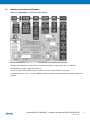
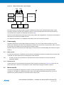
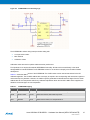
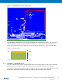
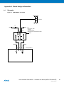
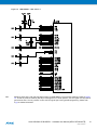
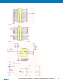
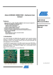
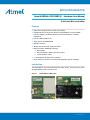
APPLICATION NOTE
Atmel AVR2044: RCB128RFA1 – Hardware User Manual
8-bit Atmel Microcontrollers
Features
•
•
•
•
•
•
•
Stand-alone operable radio controller board (RCB)
Design based on the single-chip Atmel® ATmega128RFA1 to support IEEE®
802.15.4, ZigBee®, 6LoWPAN, RF4CE, SP100, WirelessHart™, and ISM
applications
FCC-ID: VNR-S31SM-V4-00
Japan TELEC: 005WWCA0425
SMA RF connector
Simple user interface with button and LEDs
Board information EEPROM containing
• MAC address
• Board identification, features and serial number
• Crystal calibration values
•
•
2 × AAA batteries for stand-alone operation
60-pin extension connector to interface with application-specific hardware
Introduction
The RCB128RFA1 user manual describes the usage, design, and layout of the Atmel
ATmega128RFA1 radio controller board.
Figure 1.
RCB128RFA1 PCBA photo.
8339C−AVR−07/12
Table of Contents
1. Disclaimer ............................................................................................ 3 2. Overview .............................................................................................. 3 3. Mechanical description......................................................................... 4 3.1 Mechanical dimensions ..................................................................................... 4 3.2 Interface connector specifications ..................................................................... 5 3.3 Application (base) board connectors ................................................................. 6 4. Functional description .......................................................................... 6 4.1 Power supply..................................................................................................... 7 4.1.1 Battery power ...................................................................................... 7 4.1.2 External power .................................................................................... 7 4.2 Microcontroller................................................................................................... 7 4.3 On-chip radio transceiver .................................................................................. 8 4.4 Clock sources.................................................................................................... 8 4.4.1 Radio transceiver clock ....................................................................... 8 4.4.2 Microcontroller clock ........................................................................... 8 4.5 On-board peripherals ........................................................................................ 9 4.5.1 Key and LEDs ..................................................................................... 9 4.5.2 ID EEPROM........................................................................................ 9 4.6 External peripherals ........................................................................................ 11 4.7 PCB layout description .................................................................................... 13 4.7.1 PCB detail 1 – balanced RF fan out .................................................. 15 4.7.2 PCB detail 2 – balun ground connection ........................................... 16 4.7.3 PCB detail 3 – bias DC block, AC ground ......................................... 16 4.7.4 PCB detail 4 – analog GND routing .................................................. 16 4.7.5 PCB detail 5 – digital GND routing .................................................... 16 4.7.6 PCB detail 6 – ground plane ............................................................. 17 4.7.7 PCB detail 7 – crystal guard routing ................................................. 17 4.7.8 PCB detail 8 – RF section shielding .................................................. 17 4.7.9 PCB detail 9 – board ground plane design ....................................... 17 5. Programming...................................................................................... 17 6. Electrical charateristics ...................................................................... 18 6.1 Absolute maximum ratings .............................................................................. 18 6.2 Recommended operating range ...................................................................... 18 6.3 General RF specifications ............................................................................... 18 6.4 Current consumption specifications ................................................................ 18 7. Abbreviations ..................................................................................... 19 Appendix A. Board design information .............................................. 20 A.1 Schematic ....................................................................................................... 20 A.2 Assembly drawing ........................................................................................... 24 A.3 Bill of materials ................................................................................................ 25 A.4 Radio certification............................................................................................ 26 A.4.1 United States (FCC).......................................................................... 26 A.4.2 Europe (ETSI) ................................................................................... 27 A.4.3 Japan 27 A.4.4 Approved antenna ............................................................................ 27 Appendix B. EVALUATION BOARD/KIT IMPORTANT NOTICE....... 28 Appendix C. References .................................................................... 29 Appendix D. Revision history RCB128RFA1 PCBA........................... 30 Atmel AVR2044: RCB128RFA1 – Hardware User Manual [APPLICATION NOTE]
8339C−AVR−07/12
2
1.
Disclaimer
Typical values contained in this application note are based on simulations and on testing of individual examples.
Any information about third-party materials or parts is included in this document for convenience. The vendor may have
changed the information that has been published. Check the individual vendor information for the latest changes.
2.
Overview
The RCB128RFA1 is designed to provide a reference design for the Atmel ATmega128RFA1 [1] single-chip
microcontroller and radio transceiver. The IC integrates a powerful, 8-bit AVR® RISC microcontroller, an IEEE 802.15.4compliant transceiver, and additional peripheral features. The built-in radio transceiver supports the worldwide
accessible 2.4GHz ISM band.
The system is designed to demonstrate standard-based applications such as ZigBee/IEEE 802.15.4, ZigBee RF4CE,
and 6LoWPAN, as well as high data rate ISM applications. The SMA antenna connector allows either operation with the
antenna provided with the RCB or conducting RF performance measurements.
The RF section has been shielded to eliminate interference from sources external to the ATmega128RFA1. To
investigate the reference design area, the shield can be opened by removing the snap-in cover while the RCB is not in
operation.
Most peripheral features of the ATmega128RFA1 are made available through two expansion connectors (EXT0/1).
There are a variety of base boards available for the RCB family.
Table 2-1.
RCB base boards.
Board name
Comment
RCB Sensor Terminal Board
Available with Atmel evaluation kit ATRF4CE-EK; [8]
RCB Key Remote Control
Available with Atmel evaluation kit ATRF4CE-EK; [9]
RCB Breakout Board
Purchasable on http://www.dresden-elektronik.de
RCB Breakout Board Light
Purchasable on http://www.dresden-elektronik.de
Figure 2-2. RCB128RFA1 with snap-in cover removed.
Atmel AVR2044: RCB128RFA1 – Hardware User Manual [APPLICATION NOTE]
8339C−AVR−07/12
3
3.
Mechanical description
RCBs demonstrating radio transceiver and microcontroller capabilities are equipped with two 50mil, 30-pin connectors
(ETX0/1), separated by 22mm from each other, to interface to various port extension boards (base boards).
The RCB128RFA1 has no on-board antenna, and so it is not required to separate the board into an electronics section
and an antenna section. When used with a quarter-wave antenna mounted at the SMA connector, the board will act as
a ground plane for the antenna.
The other mounting hole is reserved for a battery holder. If battery operation is required, base boards should not make
use of this mount.
3.1
Mechanical dimensions
Figure 3-1shows the EXT0/1 interface connector positions referenced to pin 1, as most CAD tools use this pin as a
placement reference. Please pay attention to the connector key location at pin 30 and the mirrored placement of a male
counterpart connector when designing a new base board. The connector pin 1 is marked using a rectangular pad.
See Figure 3-2 and Figure 7-5.
The PCB is made of standard 1.5mm FR4 material with two copper layers. Due to the panelization and cutting process,
the dimension of the outer board edge may vary up to ±0.1mm.
Figure 3-1. RCB128RFA1 – mechanical drawing (dimensions in mm).
Atmel AVR2044: RCB128RFA1 – Hardware User Manual [APPLICATION NOTE]
8339C−AVR−07/12
4
3.2
Interface connector specifications
Figure 3-2. RCBA128RFA1 – interface connector drawing.
The base board interface connector, EXT0/1, mounted on the RCB, is a 50mil, 30-pin type from SAMTEC.
The detailed part number is: SFM-115-L2-S-D-LC.
The L2 in the part number indicates the low insertion force (LIF) variant to allow easy mounting.
The drawing shown in Figure 3-2 is from a SAMTEC datasheet. Check the latest datasheet for possible updates and
changes.
Atmel AVR2044: RCB128RFA1 – Hardware User Manual [APPLICATION NOTE]
8339C−AVR−07/12
5
3.3
Application (base) board connectors
Figure 3-3. Application board connector drawing.
The drawing in Figure 3-3 shows the connector to be used on a base board to interface the RCB EXT0/1 connectors.
The detailed part number is: TFM-115-02-S-D.
Alternatively, a Tyco part can be used: Tyco 5-104655-4.
Note:
The Tyco part requires a different footprint design!
The drawing shown in Figure 3-3 is from a SAMTEC datasheet. Check the latest datasheet for possible updates and
changes.
4.
Functional description
Figure 4-1 illustrates the RCB setup in general. It mainly consists of an Atmel ATmega128RFA1 and some peripheral
circuitry. An ID EEPROM stores MAC address and additional board information. This information is stored in a separate
EEPROM to avoid accidental data erasure during microcontroller firmware development.
Atmel AVR2044: RCB128RFA1 – Hardware User Manual [APPLICATION NOTE]
8339C−AVR−07/12
6
Figure 4-1. Radio controller board – block diagram.
32kHz
16MHz
Expansion
Connector 1
ATmega128RFA1
Filter-Balun
Expansion
Connector 2
Pushbutton
LEDs
ID
EEPROM
The radio transceiver incorporates MAC hardware accelerators to handle all RF modulation/demodulation, signal
processing, and frame reception and transmission actions. Further information about the radio transceiver and the
microcontroller are provided in the datasheet (see reference [1]).
The RF front-end implementation was kept minimal by using a balun with integrated filter. An antenna, provided with the
RCB, has to be connected to the SMA connector.
All components are placed on one PCB side to demonstrate a low-cost manufacturing solution.
4.1
Power supply
The RCB is powered by a single supply voltage in the range of 1.8V to 3.6V, which makes it possible to use 1.5V
alkaline cells. Optionally, the power can be supplied from a base board. In this case, the power switch, SW1, must be in
the off position or the battery must be removed from the battery holder.
All PCB components are powered by this single supply to minimize the bill of materials (BOM) and maximize the power
efficiency.
4.1.1
Battery power
For autonomous operation, the RCB can be powered by two AAA batteries inserted in the battery clip on the back side
of the RCB. Use power switch SW1 to manually switch on/off the board.
Note:
4.1.2
A power cycle may not be detected if the radio transceiver and microcontroller are in sleep mode with all
peripheries disabled.
External power
An RCB mounted on a base board may be powered via the expansion connectors (see Figure 4-2). In this case, the
power switch, SW1, has to be in the off position to avoid unintentionally charging the batteries, if present.
4.2
Microcontroller
The Atmel ATmega128RFA1 integrates a low-power, 8-bit microcontroller based on the AVR enhanced RISC
architecture. The 128KB non-volatile flash program memory and 16KB internal SRAM, supported by a rich set of
peripheral units, makes it suitable for a full-function sensor network node.
Atmel AVR2044: RCB128RFA1 – Hardware User Manual [APPLICATION NOTE]
8339C−AVR−07/12
7
The microcontroller is capable of operating as a PAN-coordinator, a full-function device (FFD), or a reduced function
device (RFD), as defined by IEEE 802.15.4 [2]. However, the RCB is not limited to these, and can be programmed to
operate in other standards or ISM applications, too.
All spare I/O pins are accessible via the expansion connectors for external use.
The Atmel ATmega128RFA1 is designed to operate at full 16MHz speed over the complete supply voltage range from
1.8V to 3.6V.
4.3
On-chip radio transceiver
Besides an 8-bit AVR microcontroller, the ATmega128RFA1 also integrates an IEEE 802.15.4-compliant radio
transceiver. RF and baseband critical components are integrated to transmit and receive signals according to IEEE
802.15.4 or proprietary ISM data rates.
The RCB illustrates a minimal component count implementation. Filter-balun B1 [6] operates as a differential to singleended converter connecting the ATmega128RFA1 to a standard SMA connector. An integrated harmonic filter ensures
sufficient harmonic rejection.
A 2.45GHz ISM antenna must be connected to the SMA connector for proper operation.
Any modification of components, PCB layout, or shielding may influence the performance of the circuitry and cause
existing certifications to be invalid.
4.4
Clock sources
4.4.1
Radio transceiver clock
The integrated radio transceiver is clocked by a highly accurate 16MHz reference crystal, Q2. Operating the node
according to IEEE 802.15.4, the reference frequency deviation must be within ±40ppm (see [2]). The absolute clock
frequency is mainly determined by the external load capacitance of the crystal, which depends on the crystal type and is
given in its datasheet.
The radio transceiver reference crystal, Q2, must be isolated from fast switching digital signals and surrounded by a
grounded guard trace to minimize disturbance of the oscillation.
The RCB uses a SIWARD SX4025 crystal with two load capacitors of 10pF each. To compensate for fabrication and
environment variations, the frequency can be tuned with the transceiver register, XOSC_CTRL (0x12) (see [1]). An
initial tuning is done during fabrication, and the correction value has been stored in the onboard ID EEPROM (see
Section 4.5.2).
By setting the fuses accordingly, the microcontroller can also be clocked by the 16MHz radio reference crystal.
4.4.2
Microcontroller clock
The Atmel ATmega128RFA1 provides several clock source options for the internal microcontroller:
•
•
•
16MHz calibrated internal RC oscillator
128kHz internal RC oscillator
16MHz radio reference crystal
The calibrated internal RC oscillator, pre-scaled to 8MHz, is used as the default clocking. It is recommended to use the
MAC symbol counter (see [1]) clocked from the 16MHz radio reference crystal as a reference to calibrate the RC
oscillator for higher accuracy.
The symbol counter replaces and enhances the CLKM-driven timer1 function originally available in ATmega1281Vbased solutions.
Atmel AVR2044: RCB128RFA1 – Hardware User Manual [APPLICATION NOTE]
8339C−AVR−07/12
8
A 32kHz crystal, Q1, is connected to the related Atmel ATmega128RFA1 pins (17-TOSC2; 18-TOSC1) to be used as a
low-power, real-time clock. This time base can also run in sleep mode and create timer-based system wake-up events.
4.5
On-board peripherals
4.5.1
Key and LEDs
For simple applications and debugging purposes, or just to deliver status information, a basic user interface is provided
directly on board, and consists of four LEDs and a pushbutton. Three LEDs (D2…D4) are connected to PE2…PE4 for
active-low operation. One LED (D5) signals the single-chip reset state. The pushbutton, T1, pulls PE5 to GND, and is
intended to be used in combination with the internal pull-up resistor.
When mounted on a base board, I/O ports PE4 and PE5 are used to emulate #WR and #RD lines handling a memory
interface. Therefore, the pushbutton and LED D4 are not functional. On RCB128RFA1, the port G I/O lines cannot be
used because they are shared with dedicated radio transceiver functionality.
In sleep mode, when the signals are supposed to be inactive, no additional current occurs.
Figure 4-2. RCB128RFA1 key and LED connection.
4.5.2
ID EEPROM
Firmware-based board type identification is supported by an optional identification EEPROM. Information about the
RCB itself, MAC addresses, and production calibration data are stored there. An Atmel AT25010A EEPROM [7] with
128 × 8-bit organization and SPI interface is used because of its small package, low voltage, and low-power operation.
Compared to Atmel Atmega1281V-based RCBs, the ID EEPROM interface has been designed in a different way.
Accessing the ID EEPROM requires PG5 set to logic low. This pin is not used on Atmega1281V-based RCBs
(see Figure 4-3 for details).
Atmel AVR2044: RCB128RFA1 – Hardware User Manual [APPLICATION NOTE]
8339C−AVR−07/12
9
Figure 4-3. ID EEPROM access decoding logic.
The ID EEPROM is written during board production testing with:
•
•
•
A unique serial number
MAC address
Calibration values
Calibration values are used to optimize radio transceiver performance.
Final products do not require this external ID EEPROM functionality. All data can be stored directly in the Atmel
Atmega128RFA1 internal EEPROM. The ID EEPROM is there for convenience to simplify microcontroller firmware
development.
Table 4-1 shows the data structure of the ID EEPROM. The Cal RC values can be used as start values for the RC
calibration algorithm. The Cal OSC 16MHz value can simply be copied to the corresponding radio transceiver register to
reduce the frequency deviation. However, the 16MHz crystal is guaranteed to deviate less than 20ppm from the actual
16MHz value at room temperature without any calibration adjustment. When the Cal OSC 16MHz value is applied, the
deviation is less than 5ppm at room temperature.
Table 4-1.
ID EEPROM mapping.
Address
Name
Type
Description
0x00
MAC address
uint64
MAC address (1) for the 802.15.4 node, little endian byte order
0x08
Serial number
uint64
Board serial number, little endian byte order
0x10
Board family
uint8
Internal board family identifier
0x11
Revision
uint8
Board revision number, for example 06 03 01
Atmel AVR2044: RCB128RFA1 – Hardware User Manual [APPLICATION NOTE]
8339C−AVR−07/12
10
Address
Name
Type
Description
0x14
Feature
uint8
Board features, coded into 7 bits
7
Reserved
6
Reserved
5
External LNA
4
External PA
3
Reserved
2
Diversity
1
Antenna
0
SMA connector
0x15
Cal OSC 16MHz
uint8
RF231 XTAL calibration value, register XTAL_TRIM
0x16
Cal RC 3.6V
uint8
AVR internal RC oscillator calibration value
@ 3.6V, register OSCCAL
0x17
Cal RC 2.0V
uint8
AVR internal RC oscillator calibration value
@ 2.0V, register OSCCAL
0x18
Antenna gain
int8
Antenna gain [1/10dBi]
For example: 0x0A = 10d will indicate a gain of 1.0dBi. The values 00h and FFh
are per definition invalid. Zero or -0.1dBi has to be indicated as 0x01 or 0xFE
0x20
Board name
char[30]
Textual board description
0x3E
CRC
uint16
16 bit CRC checksum, standard ITU-T generator polynomial G16(x) = x16 + x12 +
x5 + 1
Note:
1.
MAC addresses used for this package are Atmel property. The use of these MAC addresses for
development purposes is permitted.
Example ID EEPROM dump:
4.6
6D 4D 17 FF FF 25 04 00 86 12 00 00 2F 00 00 00
mM...%....../...
01 06 03 01 02 00 A5 A5 00 FF FF FF FF FF FF FF
................
52 43 42 31 32 38 52 46 41 31 00 00 00 00 00 00
RCB128RFA1......
00 00 00 00 00 00 00 00 00 00 00 00 00 00 52 F2
..............R.
FF FF FF FF FF FF FF FF FF FF FF FF FF FF FF FF
................
FF FF FF FF FF FF FF FF FF FF FF FF FF FF FF FF
................
FF FF FF FF FF FF FF FF FF FF FF FF FF FF FF FF
................
FF FF FF FF FF FF FF FF FF FF FF FF FF FF FF FF
................
External peripherals
The RCB is equipped with two 50mil connectors (EXT0/1) to mount the RCB on a variety of expansion boards (base
boards). The connectors provide access to all spare Atmel Atmega128RFA1 pins, including USART, TWI, ADC, and
PWM.
Make sure that any RCB base board that is used together with the RCB128RFA1 will not drive the TST signal (EXT1,
pin5) high during operation. The only occasion to drive the TST signal high is during parallel programming. Please refer
to [1] for detailed information. For normal operation, this signal must be left open or pulled to ground. For the
unconnected case, R9 will drive the pin low.
Atmel AVR2044: RCB128RFA1 – Hardware User Manual [APPLICATION NOTE]
8339C−AVR−07/12
11
The Atmega128RFA1 does not integrate a memory controller like the Atmel Atmega1281V. A memory controller
function is to be emulated by hardware (ports A, B, and C) and software. This results in an I/O mapping if this
functionality is needed:
•
•
A memory data bus is emulated using port B
•
#RD and #WR, if needed, are emulated by PE5 and PE4
For the memory address bus emulation, only the upper four address lines can be controlled via port D. To
achieve that, the PD4..7 signals are routed to both connections, port D and C
The detailed pin mapping is shown in Table 4-2. This table also provides mapping of existing Atmega1281V-based
RCBs.
Table 4-2.
Extension connector (EXT0/1) mapping.
EXT0
Pin#
RCB128RFA1
function
1281V RCB function
Pin#
RCB128RFA1
function
1281V RCB function
1
PG0
PB6
2
PG1
PB7
3
RSTN
#RESET
4
V_RCB
V_RCB
5
GND
GND
6
Not connected
XTAL2
7
CLKI
XTAL1
8
GND
GND
9
PD0
PD0 (SCL)
10
PD1
PD1 (SDA)
11
PD2
PD2 (RXD1)
12
PD3
PD3 (TXD1)
13
PD4
PD4
14
PD5
PD5
15
PD6
PD6 (CLKM)
16
PD7
PD7
17
PE4 (#WR)
PG0 (#WR)
18
PE5 (#RD)
PG1 (#RD)
19
GND
GND
20
GND
GND
21
GND
PC0
22
GND
PC1
23
GND
PC2
24
GND
PC3
25
PD4
PC4
26
PD5
PC5
27
PD6
PC6
28
PD7
PC7
29
GND
GND
30
PG2 (ALE)
PG2 (ALE)
Pin#
RCB128RFA1
function
1281V RCB function
Pin#
RCB128RFA1
function
1281V RCB function
1
PB1
PB1 (SCK)
2
GND
GND
3
PE7
PE7
4
PE6
PE6
5
PE5
6
RSTON
PE4
7
TST (connect for
parallel
programming only)
PE3
PE3
8
PE2
PE2
9
PE1
PE1 (PDO)
10
PE0
PE0 (PDI)
11
GND
AGND
12
AREF
AREF
EXT1
Atmel AVR2044: RCB128RFA1 – Hardware User Manual [APPLICATION NOTE]
8339C−AVR−07/12
12
EXT1
Pin#
RCB128RFA1
function
1281V RCB function
Pin#
RCB128RFA1
function
1281V RCB function
13
PF0
PF0
14
PF1
PF1
15
PF2
PF2
16
PF3
PF3
17
PF4
PF4 (TCK)
18
PF5
PF5 (TMS)
19
PF6
PF6 (TDO)
20
PF7
PF7 (TDI)
21
V_RCB
V_RCB
22
GND
GND
23
PB0
PA0
24
PB1
PA1
25
PB2
PA2
26
PB3
PA3
27
PB4
PA4
28
PB5
PA5
29
PB6
PA6
30
PB7
PA7
The connector pin-out mapping enables operation with almost all peripheral elements on existing base boards, except
external SRAM support.
4.7
PCB layout description
This section discusses critical layout details, important for derived PCB designs. A derived design should carefully
consider the following details:
•
Establish a solid ground plane for the antenna. The PCB area has to be considered as a counterpart of the
antenna. The PCB interacts with the radiated electromagnetic wave
•
Isolate digital noise from the antenna and the RF and analog radio transceiver sections to ensure maximum
possible radio transceiver performance
•
Isolate digital noise from the reference crystal to ensure maximum possible transmit signal purity and receiver
performance, especially when operating in high data rate ISM modes
•
Reduce any kind of spurious emissions well below the limits set by the individual regulatory organizations
Layout details 1 to 9, as shown in Figure 4-4 and Figure 4-5, are described in the following sub-sections.
Atmel AVR2044: RCB128RFA1 – Hardware User Manual [APPLICATION NOTE]
8339C−AVR−07/12
13
2
Figure 4-4. RCB128RFA1 top layer design details.
Atmel AVR2044: RCB128RFA1 – Hardware User Manual [APPLICATION NOTE]
8339C−AVR−07/12
14
Figure 4-5. RCB128RFA1 bottom layer design details.
The RCB128RFA1 demonstrates a low-cost two-layer PCB design with a total thickness of 1.6mm. The chosen PCB
material is FR4 (ISOLA IS400). The top and bottom layer each with 35µm copper are used as ground planes.
Performance is achieved without using additional inner ground and supply planes. Figure 4-6 shows the layer stack:
Figure 4-6. PCB layer stack.
Top
35μm
≈ 1530μm
35μm
Bottom
4.7.1
PCB detail 1 – balanced RF fan out
The radio transceiver RF ports require a small serial inductance in series with the balun or antenna pins. A reasonable
inductance value is 1.2nH. With the given 1.5mm RF4 substrate, it is not possible to design a differential 100Ω
transmission line. Thus, traces between filter-balun and single chip are kept at a reasonable small width of 0.2mm. With
this approach, transmission lines are well routable and create the required inductance at the same time.
Atmel AVR2044: RCB128RFA1 – Hardware User Manual [APPLICATION NOTE]
8339C−AVR−07/12
15
4.7.2
PCB detail 2 – balun ground connection
The filter-balun requires a solid ground connection (refer to [6]). Because the filter-balun has to drive a single-ended line
towards the SMA connector, each current injected into this line creates a counterpart current into the ground plane. A
parasitic inductance to ground is, therefore, directly inserted into the signal path and increases the insertion loss.
Further, the integrated harmonic low-pass filter has to perform well at much higher frequencies to reduce harmonics.
Any parasitic inductance causes limited harmonic filter performance.
Lowest inductance is achieved with large copper areas on the top and bottom planes. Both planes are to be sewn
together with sufficient through holes, especially in close proximity of GND pins of critical RF components. Resulting
through-hole inductances are to be considered as parallel connected, resulting in the lowest possible overall
inductance.
4.7.3
PCB detail 3 – bias DC block, AC ground
The RCB uses an integrated filter-balun (refer to [6]). The component provides pin 2 as a bias port towards the
differential pins. To avoid a DC connection of the radio transceiver circuitry (refer to [1]), filter-balun pin 2 requires a DC
blocking capacitor, C1, to create an AC GND connection only.
This capacitor is to be placed as close as possible to the filter-balun to ensure a low-impedance AC connection. For the
RCB128RFA1, the minimum distance was limited by the minimum width of a solder mask separator in between the
balun and the capacitor pad. The actual value is related to the PCB manufacturer capabilities.
The grounded pad of the capacitor is surrounded by three through holes in close proximity to ensure the lowest possible
impedance.
The capacitor itself should be of size 0402, or smaller.
4.7.4
PCB detail 4 – analog GND routing
It is recommended to design the ground trace as wide as possible to avoid parasitic inductances.
Atmel ATmega128RFA1 analog ground pins are to be routed to the paddle underneath the IC. The GND trace width is
recommended to be similar to the pad width.
Each GND pin should be connected to the bottom plane with at least one through hole in direct proximity to the IC.
Soldering technology allows placing small through holes (0.15mm drill) within the ground paddle underneath the
Atmega128RFA1. Through holes are filled with solder during reflow soldering; solder paste loss is low, however, due to
the small drill size.
For pin 55 an exception should be considered since there are special conditions in its adjacent area:
•
In this area a solid GND plane does not exist on top since there are many parts located there (XTAL, load and
blocking capacitors). The GND in most cases is limited to one via and maybe some traces. This is not really
low inductance, especially on a 1.5mm double layer substrate
•
The crystal is right next to it. An increased noise level at this pin may crosstalk into the crystal
Therefore, the rule for pin 55 is that it should be handled like the digital ground pins when a solid grounding is possible
next to the package. The term ‘solid grounding’ shall be understood as a close connection to a ground plane on top and
more than one via.
If only one or no via is possible the pin shall also be connected to the paddle.
4.7.5
PCB detail 5 – digital GND routing
The digital GND pins are not directly connected to the paddle. This is to avoid dispersion of digital noise from I/O pad
cells or other digital processing units.
Atmel AVR2044: RCB128RFA1 – Hardware User Manual [APPLICATION NOTE]
8339C−AVR−07/12
16
A direct connection causes a small voltage drop for digital noise due to the limited impedance of the paddle through
holes, resulting in an increased noise floor transferred to the analog domain.
Digital ground pins should be connected to the top layer ground fill, and from there with vias to the ground plane below.
4.7.6
PCB detail 6 – ground plane
Besides acting as an electrical ground plane, the PCB area creates a counterpart pole for the antenna. Such an
antenna base plate is considered as a continuous metal plane.
Therefore it is recommended to fill any unused PCB area with copper electrically connected to GND. Both PCB sides
are to be connected using individual or, if possible, grids of through holes. By doing this, the PCB behaves like a
coherent piece of metal for an external electromagnetic field.
4.7.7
PCB detail 7 – crystal guard routing
The 16MHz radio reference crystal PCB design requires special attention to avoid the influence of external noise
sources and to keep the radiation of 16MHz harmonics low.
Any crosstalk from digital lines into the crystal signals increases the phase noise and reduces the radio transceiver
performance.
A grounded guard trace is placed around the crystal area to protect the crystal against digital noise.
To investigate the impact of digital noise on the reference crystal, it is recommended to perform packet error rate tests
with potential digital noise sources enabled and disabled. The influence of disturbances such as MCLK or SPI activity
during transmit or receive can be evaluated by comparing the measurement results.
4.7.8
PCB detail 8 – RF section shielding
A shield covering the Atmel Atmega128RFA1 and related parts is used to protect the IC from external noise and strong
interferers. The shield is not required to suppress any radiation generated by the IC.
4.7.9
PCB detail 9 – board ground plane design
A PCB ground plane with openings that are small compared to the RF wavelength can be considered as continuous.
Signal lines required for normal operation create electrically long slots within the ground plane. A PCB design should
accommodate ground sections on the opposite PCB side to short the slots. This design technique helps create a solid
antenna ground in spite of the limitations of a cost-effective two-layer board.
5.
Programming
All programming interfaces are available through two 50mil connectors (EXT0/1). Using an appropriate base board, the
interfaces are available as 100mil connectors to directly connect programming tools such as JTAGICE mkII.
Base boards with an ISP connector cannot be used for ISP with the RCB128RFA1. The Atmel Atmega128RFA1 has the
serial programming function mapped to port B. Please refer to the Atmega128RFA1 data sheet [1] for detailed pin
descriptions.
Atmel AVR2044: RCB128RFA1 – Hardware User Manual [APPLICATION NOTE]
8339C−AVR−07/12
17
6.
Electrical charateristics
6.1
Absolute maximum ratings
Stresses beyond those listed under “Absolute maximum ratings” may cause permanent damage to the RCB. This is a
stress rating only and functional operation of the device at these or any other conditions beyond those indicated in the
operational sections of this manual are not implied. Exposure to absolute maximum rating conditions for extended
periods may affect device reliability. For more details about these parameters, refer to individual datasheets of the
components used.
No.
Parameter
6.1.1
Storage temperature range
6.1.2
Humidity
6.1.3
Supply voltage
6.1.4
EXT I/O pin voltage
6.1.5
Typical
-40
Non-condensing
Maximum
Units
+85
°C
80
%
+3.6
All digital I/O signals
-0.3
V_RCB+0.3
Analog I/O pin voltage
Aref (1)
Port F pins when ADC enabled (2)
-0.3
2.0
6.1.6
Supply current from RCB
battery through EXT connectors
Sum over all power pins together
-0.5
A
6.1.7
Battery charge current
AAA NiMH Accu
AAA alkaline cell (3)
0.5
0
A
mA
6.1.8
DC voltage at RF connection
6.1.9
ESD voltage
6.1.10
Input RF level
100
HBM
1000
1.
Never drive Aref from an external source (see [1] for further details).
2.
To measure voltages up V_RCB, see PGA settings in [1].
3.
Note Section 4.1.2 if RCB is mounted to a base board.
V
V
14
dBm
Mixumum
Units
+70
°C
Recommended operating range
No.
Symbol
Parameter
Condition
6.2.1
TOP
Operating temperature
range
16MHz within ±40ppm
-20
6.2.2
V_RCB
fRF
Supply voltage
fCPU = 16MHz or below
1.8 (1)
6.2.3
Note:
6.3
Minimum
-0.3
Notes:
6.2
Condition
1.
Operating frequency range
Minimum
Typical
3.0
2400
3.6
V
2483.5
MHz
Minimum value assuming stand-alone operated RCB. If mounted on a base board, value may be
increased.
General RF specifications
For general RF specifications, refer to the Atmel Atmega128RFA1 datasheet [1]. The RCB schematic follows the
application circuit. The filter-balun and SMA connector result in a typical loss of 1dB in TX output power and sensitivity
compared to the values as shown in the radio transceiver section.
6.4
Current consumption specifications
Power consumption figures of the individual Atmel Atmega128RFA1 building blocks and operation conditions are listed
in the datasheet [1].
To determine the RCB current consumption, the following values are to be taken into account:
Test conditions (unless otherwise stated) (1) (2):
Atmel AVR2044: RCB128RFA1 – Hardware User Manual [APPLICATION NOTE]
8339C−AVR−07/12
18
VDD = 3.0V, TOP = 25°C.
No.
Symbol
Parameter
Condition
Current per LED when
driving port pin is low
6.4.1
ILED
LED on current
6.4.2
IEE_SLEEP
ID EEPROM standby
current
Notes:
Minimum
1.
Current consumption figures does not include microcontroller.
2.
Current consumption for all operating modes is reduced at lower VDD.
Typical
Mixumum
Units
3
mA
1.5
µA
The RCB does not provide any external pull-up or pull-down resistors needed to be driven in a static way. However, the
software has to ensure proper port settings to avoid floating I/O lines.
After resetting the Atmega128RFA1, I/O ports are set as inputs and are floating. This may result in increased current
consumption. It is recommended to either enable internal pull-up resistors or to configure I/O ports as outputs
immediately after reset.
7.
Abbreviations
AAA
-
Battery size, also known as IEC R03 or JIS UM 4
ADC
-
Analog-to-digital converter
EEPROM
-
Erasable electrical programmable read-only memory
FCC
-
Federal Communication Commission
FFD
-
Full functional device
HBM
-
Human body model
ISM
-
Industrial, scientific, and medical
ISP
-
In system programming
LNA
-
Low-noise amplifier
MAC
-
Medium access control
PA
-
Power amplifier
PAN
-
Personal area network
PCB
-
Printed circuit board
PCBA
-
Printed circuit board assembled
RCB
-
Radio controller board
RF
-
Radio frequency
RX
-
Receive
SMA
-
Subminiature version A
SOC
-
System on chip
TWI
-
Two-wire serial interface
TX
-
Transmit
USART
-
Universal synchronous/asynchronous receiver/transmitter
XTAL
-
(Reference) crystal
Atmel AVR2044: RCB128RFA1 – Hardware User Manual [APPLICATION NOTE]
8339C−AVR−07/12
19
Appendix A. Board design information
A.1
Schematic
Figure 7-1. RCB128RFA1 – RF section.
DGND DGND
1
X1
SMA Vertical
DGND DGND
C1
DGND
DGND
B1
Balun+Filter_SMD
Johanson
2450FB15L0001E
Alternativ: W³rth 748421245; de19256
22p
6
nc
DGND
DGND
DGND
ATmega128RFA1
Atmel AVR2044: RCB128RFA1 – Hardware User Manual [APPLICATION NOTE]
8339C−AVR−07/12
20
Figure 7-2. RCB128RFA1 – SOC section 1.
Note:
Please be aware of the TST and CLKI signal routing on RCB128RFA1. The connector mapping is visible in Figure
7-4, as well as pull-down resistors (R8, R9) for both signals. For normal operation, the TST signal must be pulled to
ground all the time. The only occasion to drive the TST signal high is during parallel programming. Please refer
to [1] for detailed information.
Atmel AVR2044: RCB128RFA1 – Hardware User Manual [APPLICATION NOTE]
8339C−AVR−07/12
21
Figure 7-3. RCB128RFA1 – SOC section 2.
Atmel AVR2044: RCB128RFA1 – Hardware User Manual [APPLICATION NOTE]
8339C−AVR−07/12
22
Figure 7-4. RCB128RFA1 – power, I/O, and ID EEPROM.
Atmel AVR2044: RCB128RFA1 – Hardware User Manual [APPLICATION NOTE]
8339C−AVR−07/12
23
A.2
Assembly drawing
Figure 7-5. RCB128RFA1 – assembly drawing.
Atmel AVR2044: RCB128RFA1 – Hardware User Manual [APPLICATION NOTE]
8339C−AVR−07/12
24
A.3
Bill of materials
Table 7-1.
Bill of materials.
Designator
Description
B1
Comment
Qty.
Manufacuturer
P/N
Balun-Filter_SMD
1
Johansen
2450FB15L0001E
2 × AAA
1
COMF
BH-421-3
Batt1
Battery
C1, C3, C5
Capacitor
22pF
3
generic 0402
C2
Capacitor
22nF
1
generic 0402
C4, C7
Capacitor
1µF
2
generic 0603
C6, C10
Capacitor
100pF
2
generic 0402
C8, C9, C11,
C12, C13, C14,
C15, C18, C19
Capacitor
100nF
9
generic 0402
C16
Electrolytic capacitor
47µF/10V
1
D1
Schottky diode
n.i.
1
red
AVX
47µF/10V
4
Vishay
TLMS1000-GS08
SFM-115-L2-S-D-LC
2
SAMTEC
SFM-115-L2-S-D-LC
L1
Würth74279266
1
Würth
74279266
Plug1, Plug2
AMP 2-331677-2
2
AMP
2-331677-2
D2, D3, D4, D5
EXT0, EXT1
15 x 2-pin.
Q1
Crystal
CFPX-157
1
Farnell
CFPX-157
Q2
Crystal
16MHz / CL = 10pF
1
Siward
A207-011
R1, R8, R9
Resistor
10kΩ
3
R2
Resistor
n.i.
1
R3
Resistor
10kΩ
1
generic 0402
R4
Resistor
0Ω
1
generic 0402
R5, R6, R7, R10
Resistor
470Ω
4
generic 0402
Shield_BMIS
1
LairdTech
LT08AD4303
Eao09.10201.02
1
EAO
09.10201.02
ITT KSR211GLFS
1
ITT
KSR211GLFS
AT25010A
1
ATMEL
AT25010A
ATmega128RFA1
1
ATMEL
ATmega128RFA1-ZU00
19-46-1-TGG
SH1
generic 0402
SW1
SPDT
T1
Button SPST
U2
EEPROM
U3
AVR and transceiver
X1
RF conn.
SMA Vertical
1
Multicomp.
PSTG0-2400HS
Antenna
SMA
1
Mobile Mark
Atmel AVR2044: RCB128RFA1 – Hardware User Manual [APPLICATION NOTE]
8339C−AVR−07/12
25
A.4
Radio certification
The RCB128RFA1 has received regulatory approvals for modular devices in the United States, European countries,
and Japan.
A.4.1
United States (FCC)
Compliance Statement (Part 15.19)
The device complies with Part 15 of the FCC rules. To fulfill FCC Certification requirements, an original equipment
manufacturer (OEM) must comply with the following regulations:
•
The modular transmitter must be labeled with its own FCC ID number, and, if the FCC ID is not visible when
the module is installed inside another device, then the outside of the device into which the module is installed
must also display a label referring to the enclosed module
•
This exterior label can use wording such as the following. Any similar wording that expresses the same
meaning may be used
Contains FCC-ID: VNR-S31SM-V4-00
This device complies with Part 15 of the FCC Rules. Operation is subject to the following two conditions:
(1) this device may not cause harmful interference, and (2) this device must accept any interference
received, including interference that may cause undesired operation.
The device has been tested and approved with an external antenna as declared in the test report and manual. The
device may be integrated with other custom design antennas, which OEM manufacturer must authorize following the
FCC 15.21 requirements.
In this case, the OEM manufacturer must ensure that the OEM modular transmitter must be labeled with its own FCC ID
number. This includes a clearly visible label on the outside of the final product enclosure that displays the contents
shown below.
FCC-ID: <own FCC ID number>
This equipment complies with Part 15 of the FCC Rules. Operation is subject to the following two
conditions: (1) this device may not cause harmful interference, and (2) this device must accept any
interference received, including interference that may cause undesired operation. The internal / external
antenna(s) used for this mobile transmitter must provide a separation distance of at least 20cm from all
persons and must not be co-located or operating in conjunction with any other antenna or transmitter.
If the FCC ID is not visible when the equipment is installed inside another device, then the outside of the device into
which the equipment is installed must also display a label referring to the enclosed equipment.
Installers must be provided with antenna installation instructions and transmitter operating conditions for satisfying RF
exposure compliance.
Use in portable exposure conditions (FCC 2.1093) requires separate equipment authorization.
Compliance Statement (Part 15.105(b))
This equipment has been tested and found to comply with the limits for a Class B digital device, pursuant to Part 15 of
the FCC Rules. These limits are designed to provide reasonable protection against harmful interference in a residential
installation. This equipment generates uses and can radiate radio frequency energy and, if not installed and used in
accordance with the instructions, may cause harmful interference to radio communications. However, there is no
guarantee that interference will not occur in a particular installation.
Atmel AVR2044: RCB128RFA1 – Hardware User Manual [APPLICATION NOTE]
8339C−AVR−07/12
26
If this equipment does cause harmful interference to radio or television reception, which can be determined by turning
the equipment off and on, the user is encouraged to try to correct the interference by one or more of the following
measures:
•
•
•
•
Reorient or relocate the receiving antenna
Increase the separation between the equipment and receiver
Connect the equipment into an outlet on a circuit different from that to which the receiver is connected
Consult the dealer or an experienced radio/TV technician for help
(Part 15.21)
Warning:
Changes or modifications not expressly approved by this company could void the user’s authority to operate the
equipment.
A.4.2
Europe (ETSI)
If the device is incorporated into a product, the manufacturer must ensure compliance of the final product to the
European harmonized EMC and low-voltage/safety standards. A Declaration of Conformity must be issued for each of
these standards and kept on file as described in Annex II of the R&TTE Directive.
The manufacturer must maintain a copy of the device documentation and ensure the final product does not exceed the
specified power ratings, antenna specifications, and/or installation requirements as specified in the user manual. If any
of these specifications are exceeded in the final product, a submission must be made to a notified body for compliance
testing to all required standards. The “CE“ marking must be affixed to a visible location on the OEM product. The CE
mark shall consist of the initials "CE" taking the following form:
•
If the CE marking is reduced or enlarged, the proportions given in the above graduated drawing must be
respected
•
The CE marking must have a height of at least 5mm except where this is not possible on account of the nature
of the apparatus
•
The CE marking must be affixed visibly, legibly, and indelibly
More detailed information about CE marking requirements you can find at "DIRECTIVE 1999/5/EC OF THE
EUROPEAN PARLIAMENT AND OF THE COUNCIL" on 9 March 1999 at section 12.
A.4.3
Japan
The RCB128RFA1, classified as radio equipment specified in the Certification Ordinance Article 2-1-19, has received
type-based certificate for all PSDU rates under the provisions of Article 38-24 of the Radio Law.
The certificate number is 005WWCA0425.
A.4.4
Approved antenna
The device has been tested and approved for use with the antenna listed below. The device may be integrated with
other custom design antennas which OEM installer must authorize with respective regulatory agencies. The used
antenna is connected to the radio module via an SMA connection.
Table 7-2.
Approved antenna.
Manufacturer
Description
Model
Frequency
Connector
Mobile Mark
¼-wave stub antenna
PSTG0-2400HS
2400 - 2490MHz
Male SMA
Atmel AVR2044: RCB128RFA1 – Hardware User Manual [APPLICATION NOTE]
8339C−AVR−07/12
27
Appendix B. EVALUATION BOARD/KIT IMPORTANT NOTICE
This evaluation board/kit is intended for use for FURTHER ENGINEERING, DEVELOPMENT, DEMONSTRATION, OR
EVALUATION PURPOSES ONLY. It is not a finished product and may not (yet) comply with some or any technical or
legal requirements that are applicable to finished products, including, without limitation, directives regarding
electromagnetic compatibility, recycling (WEEE), FCC, CE or UL (except as may be otherwise noted on the board/kit).
Atmel supplied this board/kit “AS IS,” without any warranties, with all faults, at the buyer’s and further users’ sole risk.
The user assumes all responsibility and liability for proper and safe handling of the goods. Further, the user indemnifies
Atmel from all claims arising from the handling or use of the goods. Due to the open construction of the product, it is the
user’s responsibility to take any and all appropriate precautions with regard to electrostatic discharge and any other
technical or legal concerns.
EXCEPT TO THE EXTENT OF THE INDEMNITY SET FORTH ABOVE, NEITHER USER NOR ATMEL SHALL BE
LIABLE TO EACH OTHER FOR ANY INDIRECT, SPECIAL, INCIDENTAL, OR CONSEQUENTIAL DAMAGES.
No license is granted under any patent right or other intellectual property right of Atmel covering or relating to any
machine, process, or combination in which such Atmel products or services might be or are used.
Mailing Address: Atmel Corporation, 2325 Orchard Parkway, San Jose, CA 95131
Copyright © 2012, Atmel Corporation
Atmel AVR2044: RCB128RFA1 – Hardware User Manual [APPLICATION NOTE]
8339C−AVR−07/12
28
Appendix C. References
[1] ATmega128RFA1; 8-bit AVR Microcontroller with Low Power 2.4GHz Transceiver for ZigBee, IEEE 802.15.4,
6LoWPAN, RF4CE, SP100, WirelessHART and ISM Applications; Preliminary Datasheet; Rev. 8266D-MCU
Wireless-06/12; Atmel Corporation.
[2] IEEE Std 802.15.4™-2006: Wireless Medium Access Control (MAC) and Physical Layer (PHY) Specifications
for Low-Rate Wireless Personal Area Networks (LR-WPANs).
[3] FCC Code of Federal Register (CFR); Part 47; Section 15.35, Section 15.205, Section 15.209, Section 15.231,
Section 15.247, and Section 15.249. United States.
[4] ETSI EN 300 328, Electromagnetic Compatibility and Radio Spectrum Matters (ERM); Wideband Transmission
Systems; Data transmission equipment operating in the 2.4GHz ISM band and using spread spectrum
modulation techniques; Part 1-3.
[5] ARIB STD-T66, Second Generation Low Power Data Communication System/Wireless LAN System
1999.12.14 (H11.12.14) Version 1.0.
[6] 2.45 GHz Harmonic Filter-Balun; Datasheet 2450FB15L0001; Johanson Technology, Inc.
[7] AT25010A; SPI Serial EEPROM; Datasheet; Rev. 3348J SEEPR 8/06; Atmel Corporation.
[8] AVR2063; Sensor Terminal Board – Hardware User’s Manual; Application Note; Rev. 8359B AVR 11/11; Atmel
Corporation.
[9] AVR2037: RCB Key Remote Control – Hardware User Manual; Application Note; Rev. 8356A AVR 02/11;
Atmel Corporation
Atmel AVR2044: RCB128RFA1 – Hardware User Manual [APPLICATION NOTE]
8339C−AVR−07/12
29
Appendix D. Revision history RCB128RFA1 PCBA
Version
Description
A09-1264/01
Internal revision
A09-1264/02
Initially published revision
A09-1264/03
Internal revision
A09-1264/04
Replacement of ATmega128RFA1 rev. D by ATmega128RFA1 rev. F
Atmel AVR2044: RCB128RFA1 – Hardware User Manual [APPLICATION NOTE]
8339C−AVR−07/12
30
Atmel Corporation
Atmel Asia Limited
Atmel Munich GmbH
Atmel Japan G.K.
1600 Technology Drive
Unit 01-5 & 16, 19F
Business Campus
16F Shin-Osaki Kangyo Bldg.
San Jose, CA 95110
BEA Tower, Millennium City 5
Parkring 4
1-6-4 Osaki, Shinagawa-ku
USA
418 Kwun Tong Road
D-85748 Garching b. Munich
Tokyo 141-0032
Tel: (+1)(408) 441-0311
Kwun Tong, Kowloon
GERMANY
JAPAN
Fax: (+1)(408) 487-2600
HONG KONG
Tel: (+49) 89-31970-0
Tel: (+81)(3) 6417-0300
www.atmel.com
Tel: (+852) 2245-6100
Fax: (+49) 89-3194621
Fax: (+81)(3) 6417-0370
Fax: (+852) 2722-1369
© 2012 Atmel Corporation. All rights reserved. / Rev.: 8339C−AVR−07/12
Atmel®, Atmel logo and combinations thereof, Enabling Unlimited Possibilities®, AVR®, and others are registered trademarks or trademarks of Atmel Corporation
or its subsidiaries. Other terms and product names may be trademarks of others.
Disclaimer: The information in this document is provided in connection with Atmel products. No license, express or implied, by estoppel or otherwise, to any intellectual property right is granted by this
document or in connection with the sale of Atmel products. EXCEPT AS SET FORTH IN THE ATMEL TERMS AND CONDITIONS OF SALES LOCATED ON THE ATMEL WEBSITE, ATMEL ASSUMES
NO LIABILITY WHATSOEVER AND DISCLAIMS ANY EXPRESS, IMPLIED OR STATUTORY WARRANTY RELATING TO ITS PRODUCTS INCLUDING, BUT NOT LIMITED TO, THE IMPLIED
WARRANTY OF MERCHANTABILITY, FITNESS FOR A PARTICULAR PURPOSE, OR NON-INFRINGEMENT. IN NO EVENT SHALL ATMEL BE LIABLE FOR ANY DIRECT, INDIRECT,
CONSEQUENTIAL, PUNITIVE, SPECIAL OR INCIDENTAL DAMAGES (INCLUDING, WITHOUT LIMITATION, DAMAGES FOR LOSS AND PROFITS, BUSINESS INTERRUPTION, OR LOSS OF
INFORMATION) ARISING OUT OF THE USE OR INABILITY TO USE THIS DOCUMENT, EVEN IF ATMEL HAS BEEN ADVISED OF THE POSSIBILITY OF SUCH DAMAGES. Atmel makes no
representations or warranties with respect to the accuracy or completeness of the contents of this document and reserves the right to make changes to specifications and products descriptions at any time
without notice. Atmel does not make any commitment to update the information contained herein. Unless specifically provided otherwise, Atmel products are not suitable for, and shall not be used in,
automotive applications. Atmel products are not intended, authorized, or warranted for use as components in applications intended to support or sustain life.