1
ABOV SEMICONDUCTOR Co. Ltd.
8-BIT SINGLE-CHIP MICROCONTROLLERS
MC81F8816/8616
User’s Manual (Ver. 1.03)
Version 1.03
Published by
FAE Team
©2008 ABOV Semiconductor Co., Ltd. All rights reserved.
Additional information of this manual may be served by ABOV Semiconductor offices in Korea or Distributors.
ABOV Semiconductor reserves the right to make changes to any information here in at any time without notice.
The information, diagrams and other data in this manual are correct and reliable; however, ABOV Semiconductor is in no
way responsible for any violations of patents or other rights of the third party generated by the use of this manual.
MC81F8816/8616
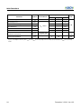
REVISION HISTORY
VERSION 1.03 (December 3, 2012) This Book
ABOV logo is renewed on this book.
Single and Gang writer are added in "1.3 Development Tools" on page 3.
VDD voltage for sub-active mode is changed to 3.0~5.5V in "7.2 Recommended Operating Conditions" on page 21.
The notice of STOP mode is added in "23.2 STOP Mode" on page 118.
Notice:If the STOP mode is used in the program, BOD function should be disabled in the initial routine of software.
Block diagram of BOD is updated in "Figure 27-1 Block Diagram of BOD (Brown-out Detector Reset)" on page 127.
VERSION 1.02 (February 11, 2010)
The caution for the ALE pin at ISP mode is added in "31.3 Hardware Conditions to Enter the ISP Mode" on page 136.
VERSION 1.01 (January 11, 2010)
The block diagram of LCD Bias is modified in Figure 18-3 LCD Bias Control
The figures of flash writer were updated in "1. OVERVIEW" on page 1.
Config Read Voltage(VCONFIG), maximum VDD Start Voltage(VSTART) and description were added in "7.3 DC Electrical
Characteristics" on page 22.
In case AVREF voltage was less than VDD voltage for ADC, the table-note and note were added in "7.5 A/D Converter
December 3, 2012 Ver 1.03
3
MC81F8816/8616
4
December 3, 2012 Ver 1.03
MC81F8816/8616
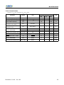
Table of Contents
1. OVERVIEW .........................................................1
Description .........................................................1
Features .............................................................1
Development Tools ............................................3
Ordering Information ........................................5
2. BLOCK DIAGRAM .............................................6
MC81F8816Q (80 pin package) .........................6
MC81F8616Q (64 pin package) .........................7
3. PIN ASSIGNMENT .............................................8
4. PACKAGE DIAGRAM ......................................10
5. PIN FUNCTION .................................................12
6. PORT STRUCTURES .......................................16
7. ELECTRICAL CHARACTERISTICS ................21
Absolute Maximum Ratings .............................21
Recommended Operating Conditions ..............21
DC Electrical Characteristics ...........................22
LCD Characteristics .........................................23
A/D Converter Characteristics .........................23
AC Characteristics ...........................................25
Serial I/O Characteristics .................................27
Typical Characteristics .....................................28
8. MEMORY ORGANIZATION .............................32
Registers ..........................................................32
Program Memory .............................................35
Data Memory ...................................................38
Addressing Mode .............................................42
9. I/O PORTS ........................................................46
Registers for Ports ...........................................46
I/O Ports Configuration ....................................47
10. CLOCK GENERATOR ...................................51
11. BASIC INTERVAL TIMER ..............................53
12. TIMER / COUNTER ........................................55
8-Bit Timer/Counter Mode ................................59
16 Bit Timer/Counter Mode ..............................61
8-Bit Capture Mode ..........................................63
16-bit Capture Mode ........................................67
8-Bit (16-Bit) Compare Output Mode ...............68
PWM Mode ......................................................68
16. BUZZER OUTPUT FUNCTION ..................... 79
17. INTERRUPTS ................................................ 81
Interrupt Sequence .......................................... 84
BRK Interrupt .................................................. 85
Multi Interrupt .................................................. 85
External Interrupt ............................................. 87
18. LCD DRIVER ................................................. 88
Control of LCD Driver Circuit ........................... 89
LCD BIAS Control ........................................... 92
LCD Display Memory ...................................... 94
Control Method of LCD Driver ......................... 95
Duty and Bias Selection of LCD Driver ........... 97
19. SERIAL PERIPHERAL INTERFACE (SPI) ... 98
Transmission/Receiving Timing ...................... 99
The usage of Serial I/O ................................. 100
The Method to Test Correct Transmission .... 101
20. INTER IC COMMUNICATION (I2C) ............. 102
Bit Transfer .................................................... 104
Start/Stop Conditions .................................... 104
Data Transfer ................................................ 105
Acknowledge ................................................. 106
Syncronization/Arbitation .............................. 107
21. UNIVERSAL ASYNCHRONOUS SERIAL INTERFACE (UART) ............................................. 110
Asynchronous Serial Interface Configuration 111
Relationship between main clock and baud rate .
114
22. OPERATION MODE .................................... 115
Operation Mode Switching ............................ 116
23. POWER DOWN OPERATION ..................... 117
SLEEP Mode ................................................. 117
STOP Mode .................................................. 118
24. OSCILLATOR CIRCUIT .............................. 122
25. PLL .............................................................. 123
External PLL Circuit ...................................... 124
13. WATCH TIMER ...............................................72
26. RESET ......................................................... 125
External Reset Input ...................................... 125
Power On Reset ............................................ 126
Brown-out Detector ....................................... 126
Watchdog Timer Reset ................................. 126
14. WATCH DOG TIMER .....................................74
27. Brown-out Detector (BOD) ........................ 127
15. ANALOG TO DIGITAL CONVERTER ............76
December 3, 2012 Ver 1.03
1
MC81F8816/8616
28. Osillation Noise Protector ..........................129
29. FLASH PROGRAMMING SPEC. .................131
FLASH Configuration Byte .............................131
FLASH Programming .....................................131
30. EMULATOR EVA. BOARD SETTING ..........133
31. IN-SYSTEM PROGRAMMING .....................134
Getting Started / Installation ...........................134
Basic ISP S/W Information .............................135
2
Hardware Conditions to Enter the ISP Mode 136
Sequence to enter ISP mode/user mode ...... 137
USB-SIO-ISP Board ...................................... 138
A. INSTRUCTION .................................................. ii
Terminology List .................................................ii
Instruction Map .................................................. iii
Instruction Set ....................................................v
B. MASK ORDER SHEET(MC81C8816) ............ xiii
C. MASK ORDER SHEET(MC81C8616) ............ xiv
December 3, 2012 Ver 1.03
MC81F8816/8616
MC81F8816/8616
CMOS SINGLE-CHIP 8-BIT MICROCONTROLLER
WITH LCD CONTROLLER/DRIVER
1. OVERVIEW
1.1 Description
The MC81F8816/8616 are an advanced CMOS 8-bit microcontroller with 16K bytes of FLASH ROM(MTP). This device is
one of the MC800 family and a powerful microcontroller which provides a high flexibility and cost effective solution to many
LCD applications. The MC81F8816/8616 provide the following standard features: 16K bytes of FLASH ROM, 512 bytes of
RAM, 40 bytes of segment LCD display RAM, 8/16-bit timer/counter, 10-bit A/D converter, 7-bit watch dog timer, 21-bit
watch timer with 7-bit auto reload counter, I2C, SPI, 8-bit UART, PLL, on-chip oscillator and clock circuitry. In addition,
this device supports power saving modes to reduce power consumption. So the MC81F8816/8616 is the best controller solution in system which uses charatered LCD display and ADC.
FLASH MCU
MASK MCU
Memory
(Bytes)
ROM
RAM
ADC
PWM
UART/
SPI/
I2C
I/O
LCD
Package
MC81F8816
MC81C8816
16K
512
8ch.
2ch.
1ch/
1ch/
1ch
56
36SEG x 8COM
(40SEG x 4COM)
80MQFP
MC81F8616
MC81C8616
16K
512
5ch.
2ch.
1ch/
1ch/
1ch
48
28SEG x 8COM
(32SEG x 4COM)
64MQFP
64LQFP
1.2 Features
• 16K Bytes On-chip FLASH ROM (ISP)
• FLASH Memory
- Endurance : 1000 cycles
- Data Retention : 10 years
• 512 Bytes On-chip Data RAM
• 40 bytes Display RAM
• 32 MHz PLL Oscillator
• Instruction Cycle Time
- 167ns at 12MHz (NOP instruction)
• LCD display/controller
- 1/4 Duty Mode (40Seg × 4Com, 1/3 Bias)
- 1/8 Duty Mode (36Seg × 8Com, 1/4 Bias)
• One 21-bit Watch Timer
- 1 minute interrupt available
• One 8-bit Basic Interval Timer
• One 6-bit Buzzer Driving Port
• Dual Clock Operation
- Main Clock : 400kHz ~ 12MHz
- Sub Clock : 32.768kHz
• Main Clock Oscillation
- Crystal
- Ceramic Resonator
- Internal Oscillation : 8MHz/4MHz
• Operating Temperature : -40~85 °C
• Four 8-bit Timer/Counter
(They can be used as two 16-bit Timer/Counter)
• Built-in Noise Immunity Circuit
- Noise Filter
- BOD(Brown-out Detector)
• One 7-bit Watch Dog Timer
• Power Down Mode
December 3, 2012 Ver 1.03
1
MC81F8816/8616
- Main Clock : STOP, SLEEP, SUB-Active mode
• 400kHz to 12MHz Wide Operating Frequency
• On-Chip POR (Power On Reset) and
BOR(Brown Out Reset)
• Internal Resistor for LCD Bias
• 56/48 Programmable I/O Pins
MC81F8816
MC81F8616
MC81C8616
I/O: 31
I:1
I/O with SEG/COM:24
I/O: 23
I:1
I/O with SEG/COM:24
• 8/5-channel 10-bit On-chip A/D Converter
• Two 10-bit High Speed PWM Output
• 16 Interrupt sources
- External Interrupt : 4
- Timer : 4
- UART : 2
- I2C, SPI, ADC, WDT, WT, BIT
• One Universal Asynchronous Receiver/Transmitter (UART)/ One Serial Peripheral Interface(SPI)/ One Inter IC Communication(I2C)
• Wide Operating Voltage & Frequency Range
- 2.2 ~ 5.5V @ (4.2Mhz)
- 4.5 ~ 5.5V @ (12Mhz)
• 80MQFP, 64MQFP, 64LQFP Package Types
- Available Pb free package
MC81F8816
8-channel ADC
MC81F8816
80MQFP
MC81F8616
MC81C8616
5-channel ADC
MC81F8616
MC81C8616
64MQFP, 64LQFP
2
December 3, 2012 Ver 1.03
MC81F8816/8616
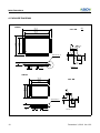
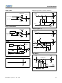
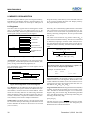
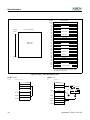
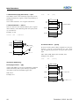
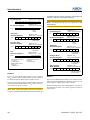
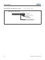
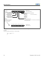
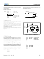
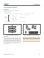
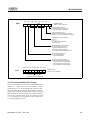
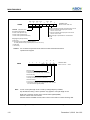
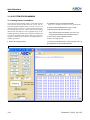
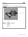
1.3 Development Tools
The MC81F8816/8616 are supported by a full-featured
macro assembler, an in-circuit emulator CHOICE-Dr.TM
and OTP/FLASH programmers. There are two different
type of programmers such as single type and gang type.
For mode detail, Macro assembler operates under the MSWindows 95 and upversioned Windows OS. And
HMS800C compiler only operates under the MS-Windows
2000 and upversioned Windows OS.
Please contact sales part of ABOV semiconductor.
Software
- MS-Windows based assembler
- MS-Windows based Debugger
- MC800 C compiler
Hardware
(Emulator)
- CHOICE-Dr.
- CHOICE-Dr. EVA81F88 B/D Rev2.0
POD Name
- POD80C73D-80MQ
- POD80C74D-64MQ
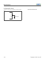
FLASH Writer
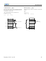
Figure 1-2 PGMplus USB ( Single Writer )
- PGM Plus USB (Single writer)
- Stand Alone PGM Plus(Single writer)
- Standalone GANG4/8 USB
(Gang writer)
- USB-SIO-ISP Board
Figure 1-3 Stand Alone PGM_Plus(ISP)
Figure 1-1 Choice-Dr. (Emulator)
December 3, 2012 Ver 1.03
3
MC81F8816/8616
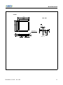
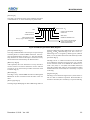
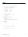
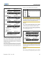
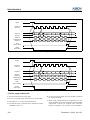
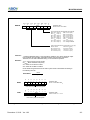
Figure 1-4 Standalone Gang4 USB (Gang Writer)
Figure 1-6 USB-SIO-ISP Board
Figure 1-5 Standalone Gang8 (Gang Writer)
4
December 3, 2012 Ver 1.03
MC81F8816/8616
1.4 Ordering Information
Device name
ROM Size
RAM size
Package
FLASH version
MC81F8816Q
MC81F8616Q
MC81F8616L
16K bytes
512 bytes
80MQFP
64MQFP
64LQFP
MASK version
MC81C8616Q
MC81C8616L
16K bytes
512 bytes
64MQFP
64LQFP
- Pb free package;
The “P” suffix will be added at original part number.
For example; MC81F8816Q(Normal package), MC81F8816Q P(Pb free package)
December 3, 2012 Ver 1.03
5
MC81F8816/8616
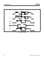
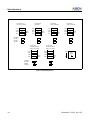
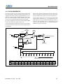
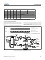
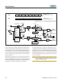
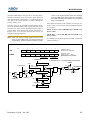
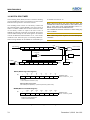
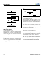
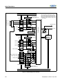
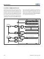
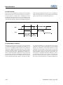
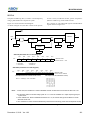
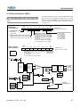
2. BLOCK DIAGRAM
2.1 MC81F8816Q (80 pin package)
Segment Drive Output
SEG0 ~ SEG35
(SEG0 ~ SEG39)
Common Drive Output
COM0 ~ COM7
(COM0 ~ COM3)
BIAS selection circuit
Internal Resistor
LCD Controller/Driver
for LCD Bias
VDD
AVref
VSS
Power
Supply
Power
Supply
Circuit
PSW
Accumulator
ALU
Stack Pointer
LCD
Display
Memory
Interrupt Controller
RESET
PC
Data
Memory
System controller
Program
Memory
Data Table
8-bit Basic
Interval Timer
System
Clock Controller
Timing generator
XIN
XOUT
SXIN
SXOUT
PLLC
High freq.
Low freq.
POR
&
BOD
6
Clock
Generator
PC
Watch/Watch Dog
Timer
I2C
PLL
10-bit A/D
Converter
8/16-bit
SIO UART PWM Timer/Counter
R7
R6
R5
R4
R2
R1
R0
8
8
8
8
8
8
8
R70
R71
R72
R73
R74
R75
R76
R77
R60
R61
R62
R63
R64
R65
R66
R67
R50
R51
R52
R53
R54
R55
R56
R57
R40
R41 / INT3
R42
R43 / SXIN
R44 / SXOUT
R45 / XIN
R46 / XOUT
R47 / RESETB
R20 / AN0
R21 / AN1
R22 / AN2
R23 / AN3
R24 / AN4
R25 / AN5
R26 / AN6
R27 / AN7
R10 / PWM1 / T2O
R11/ACK/SCK
R12 / TX0 / SOUT
R13 / RX0 / SI
R14
R15
R16 / SDA
R17 / SCL
Buzzer
Driver
R00 / PWM0 /T0O
R01 / EC0
R02
R03
R04 / BUZO
R05 / EC1/ INT0
R06 / INT1
R07 / INT2
December 3, 2012 Ver 1.03
MC81F8816/8616
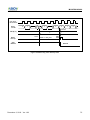
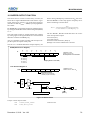
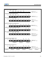
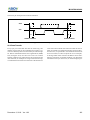
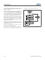
2.2 MC81F8616Q (64 pin package)
Segment Drive Output
SEG0 ~ SEG27
(SEG0 ~ SEG31)
Common Drive Output
COM0 ~ COM7
(COM0 ~ COM3)
BIAS selection circuit
Internal Resistor
LCD Controller/Driver
for LCD Bias
VDD
AVref
VSS
Power
Supply
Power
Supply
Circuit
PSW
Accumulator
ALU
Stack Pointer
LCD
Display
Memory
Interrupt Controller
RESET
PC
Data
Memory
System controller
Program
Memory
Data Table
8-bit Basic
Interval Timer
System
Clock Controller
Timing generator
XIN
XOUT
SXIN
SXOUT
PLLC
High freq.
Low freq.
POR
&
BOD
Clock
Generator
PC
Watch/Watch Dog
Timer
I2C
PLL
10-bit A/D
Converter
8/16-bit
SIO UART PWM Timer/Counter
R7
R6
R5
R4
R2
R1
R0
8
8
8
6
5
8
5
R70
R71
R72
R73
R74
R75
R76
R77
R60
R61
R62
R63
R64
R65
R66
R67
R50
R51
R52
R53
R54
R55
R56
R57
December 3, 2012 Ver 1.03
R42
R43 / SXIN
R44 / SXOUT
R45 / XIN
R46 / XOUT
R47 / RESETB
R20 / AN0
R21 / AN1
R22 / AN2
R23 / AN3
R24 / AN4
R10/PWM1/T2O
R11/ACK/SCK
R12 / TX0 / SOUT
R13 / RX0 / SI
R14
R15
R16 / SDA
R17 / SCL
Buzzer
Driver
R00 / PWM0 /T0O
R04 / BUZO
R05 / EC1/ INT0
R06 / INT1
R07 / INT2
7
SEG25
SEG24
SEG23/R77
SEG22/R76
SEG21/R75
SEG20/R74
SEG19/R73
SEG18/R72
SEG17/R71
SEG16/R70
SEG15/R67
SEG14/R66
SEG13/R65
SEG12/R64
SEG11/R63
SEG10/R62
SEG9/R61
SEG8/R60
SEG7/R57
8
VSS
R44/SXOUT
R43/SXIN
VDD
PLLC
R42
AVref
R24/AN4
R23/AN3
R22/AN2
R21/AN1
R20/AN0
R17/SCL
R16/SDA
R15
R14
R13/RX/SI
R12/TX/SOUT
R11/ACK/SCK
64MQFP
(Top View)
R45/XIN
R46/XOUT
R47/RESETB
COM0
COM1
COM2
COM3
SEG39/COM4
SEG38/COM5
SEG37/COM6
SEG36/COM7
SEG27
SEG26
52
53
54
55
56
57
58
59
60
61
62
63
64
51
50
49
48
47
46
45
44
43
42
41
40
39
38
37
36
35
34
33
R45/XIN
R46/XOUT
R47/RESETB
COM0
COM1
COM2
COM3
SEG39/COM4
SEG38/COM5
SEG37/COM6
SEG36/COM7
SEG35
SEG34
SEG33
SEG32
SEG31
64
63
62
61
60
59
58
57
56
55
54
53
52
51
50
49
48
47
46
45
44
43
42
41
65
66
67
68
69
70
71
72
73
74
75
76
77
78
79
80
1
2
3
4
5
6
7
8
9
10
11
12
13
14
15
16
17
18
19
20
21
22
23
24
VSS
R44/SXOUT
R43/SXIN
VDD
PLLC
R42
R41/INT3
R40
AVref
R27/AN7
R26/AN6
R25/AN5
R24/AN4
R23/AN3
R22/AN2
R21/AN1
R20/AN0
R17/SCL
R16/SDA
R15
R14
R13/RX/SI
R12/TX/SOUT
R11/ACK/SCK
80MQFP
(Top View)
1
2
3
4
5
6
7
8
9
10
11
12
13
14
15
16
17
18
19
SEG30
SEG29
SEG28
SEG27
SEG26
SEG25
SEG24
SEG23/R77
SEG22/R76
SEG21/R75
SEG20/R74
SEG19/R73
SEG18/R72
SEG17/R71
SEG16/R70
SEG15/R67
SEG14/R66
SEG13/R65
SEG12/R64
SEG11/R63
SEG10/R62
SEG9/R61
SEG8/R60
SEG7/R57
MC81F8816/8616
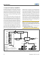
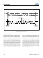
3. PIN ASSIGNMENT
MC81F8816Q
MC81F8616Q
40
39
38
37
36
35
34
33
32
31
30
29
28
27
26
25
32
31
30
29
28
27
26
25
24
23
22
21
20
R10 / PWM1 /T2O
R07 / INT2
R06 / INT1
R05 / INT0 / EC1
R04 / BUZO
R03
R02
R01 / EC0
R00 / PWM0 /T0O
SEG0/R50
SEG1/R51
SEG2/R52
SEG3/R53
SEG4/R54
SEG5/R55
SEG6/R56
R10 / PWM1 /T2O
R07 / INT2
R06 / INT1
R05 / INT0 / EC1
R04 / BUZO
R00 / PWM0 /T0O
SEG0/R50
SEG1/R51
SEG2/R52
SEG3/R53
SEG4/R54
SEG5/R55
SEG6/R56
December 3, 2012 Ver 1.03
49
50
51
52
53
54
55
56
57
58
59
60
61
62
63
64
MC81F8616L
32
31
30
29
28
27
26
25
24
23
22
21
20
19
18
17
R11 / ACK /SCK
R10 / PWM1 /T2O
R07 / INT2
R06 / INT1
R05 / INT0 / EC1
R04 / BUZO
R00 / PWM0 /T0O
SEG0/R50
SEG1/R51
SEG2/R52
SEG3/R53
SEG4/R54
SEG5/R55
SEG6/R56
SEG7/R57
SEG8/R60
SEG24
SEG23/R77
SEG22/R76
SEG21/R75
SEG20/R74
SEG19/R73
SEG18/R72
SEG17/R71
SEG16/R70
SEG15/R67
SEG14/R66
SEG13/R65
SEG12/R64
SEG11/R63
SEG10/R62
SEG9/R61
R44/SXOUT
VSS
R45/XIN
R46/XOUT
R47/RESETB
COM0
COM1
COM2
COM3
SEG39/COM4
SEG38/COM5
SEG37/COM6
SEG36/COM7
SEG27
SEG26
SEG25
1
2
3
4
5
6
7
8
9
10
11
12
13
14
15
16
64LQFP
(Top View)
48
47
46
45
44
43
42
41
40
39
38
37
36
35
34
33
R43/SXIN
VDD
PLLC
R42
AVref
R24/AN4
R23/AN3
R22/AN2
R21/AN1
R20/AN0
R17/SCL
R16/SDA
R15
R14
R13/RX/SI
R12/TX/SOUT
MC81F8816/8616
December 3, 2012 Ver 1.03
9
MC81F8816/8616
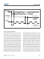
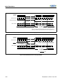
4. PACKAGE DIAGRAM
80MQFP
24.15
23.65
MAX
UNIT: MM
MIN
14.10
13.90
18.15
17.65
20.10
19.90
0-10°
0-7°
0.36
0.10
1.03
0.73
0.23
0.13
SEE DETAIL "A"
1.95
REF
3.18 max.
DETAIL “A”
0.8 BSC
0.45
0.30
64MQFP
24.15
23.65
20.10
19.90
18.15
17.65
14.10
13.90
UNIT: MM
0.36
0.10
SEE DETAIL “A”
3.18 max.
1.95
REF
0.50
0.35
10
1.03
0.73
0.23
0.13
0-7°
1.00 Typ.
DETAIL “A”
December 3, 2012 Ver 1.03
MC81F8816/8616
64LQFP
12.25
11.75
10.10
09.90
12.25
11.75
10.10
09.90
UNIT: MM
0.15
0.05
SEE DETAIL “A”
1.60 max.
1.00
REF
0.27
0.17
December 3, 2012 Ver 1.03
0.75
0.45
0.20
0.10
0-7°
0.50 Typ.
DETAIL “A”
11
MC81F8816/8616
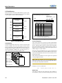
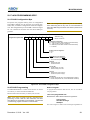
5. PIN FUNCTION
VDD: Supply Voltage.
VSS: Circuit ground.
RESET: Reset the MCU Reset.
XIN: Input to the inverting oscillator amplifier and input to
the internal main clock operating circuit.
XOUT: Output from the inverting oscillator amplifier.
SXIN: Input to the internal sub system clock operating circuit.
SXOUT: Output from the inverting subsystem oscillator
amplifier.
SEG0~SEG39: Segment signal output pins for the LCD
display. See "18. LCD DRIVER" on page 88 for details.
Also SEG0~SEG23 are shared with normal I/O ports and
SEG24~35 are only segment output port(SEG24~31 are
shared with normal I/O port at EVA chip) and SEG36~39
are multiplexed with COM7~COM4.
Note: SEG28 ~ SEG35 are not supported in
MC81F8616Q(64pin).
COM0~COM7: Common signal output pins for the LCD
display. See "18. LCD DRIVER" on page 88 for details.
Also COM0~COM3 are only common output ports and
COM4~COM7 are multiplexed with SEG36~SEG39.
COM4~COM7 and SEG36~SEG39 are selected by
LCDD0 of the LCR register.
LCDD0
0
1
COM4~COM7 / SEG39~SEG36
COM4 ~ COM7
SEG39 ~ SEG36
R00~R07: R0 is a 8-bit CMOS bidirectional I/O port(5-bit
I/O port at MC81F8616Q). R0 pins 1 or 0 written to the
Port Direction Register can be used as outputs or inputs.
Also, pull-up resistors and open-drain outputs can be assigned by software.
In addition, R0 serves the functions of the various follow-
12
ing special features.
Port pin
R00
R01
R04
R05
R06
R07
Alternate function
PWM0/T0O
(Timer1 PWM Output / Timer0 Output)
EC0 (Timer 0 Event Count Input)
BUZO (Buzzer Output)
EC1 / INT0
(Timer2 Event Count Input/External Interrupt 0 Request Input)
INT1 (External Interrupt 1 Request Input)
INT2 (External Interrupt 2 Request Input)
Note: R01/EC0~R03 are not not supported in
MC81F8616Q(64pin).
R10~R17 : R1 is an 8-bit CMOS bidirectional I/O port.
R1 pins 1 or 0 written to the Port Direction Register can be
used as outputs or inputs or schmitt trigger inputs. Also,
pull-up resistors and open-drain outputs can be assigned by
software.
In addition, R1 serves the function of the following special
fature.
Port pin
R10
R11
R12
R13
R14
R15
R16
R17
Alternate function
PWM1/T2O(Timer3 PWM / Timer2 Output)
ACK/SCK
TX/SOUT
RX/SI
SDA
SCL
R20~R27: R2 is a 5/8-bit CMOS bidirectional I/O port(5bit I/O port at MC81F8616Q). Each pins 1 or 0 written to
the Port Direction Register can be used as outputs or inputs. Also, pull-up resistors and open-drain outputs can be
assigned by software.
In addition, R2 serves the functions of the various follow-
December 3, 2012 Ver 1.03
MC81F8816/8616
units by R5PSR Register.
ing special features.
Port pin
R20
R21
R22
R23
R24
R25
R26
R27
Alternate function
Port pin
R50
R51
R52
R53
R54
R55
R56
R57
AN0 (Analog Input Port0)
AN1 (Analog Input Port1)
AN2 (Analog Input Port2)
AN3 (Analog Input Port3)
AN4 (Analog Input Port4)
AN5 (Analog Input Port5)
AN6 (Analog Input Port6)
AN7 (Analog Input Port7)
Note: R25/AN5 ~ R27/AN7 are not supported in
MC81F8616Q(64pin).
R40~R47: R4 is a 6/8-bit CMOS bidirectional I/O port(6bit I/O port at MC81F8616Q). Each pins 1 or 0 written to
the Port Direction Register can be used as outputs or inputs. Also, pull-up resistors and open-drain outputs can be
assigned by software.
In addition, R4 serves the functions of the various following special features.
Port pin
Alternate function
R40
R41
R42
R43
R44
R45
R46
R47
INT3 (External Interrupt 3 Request input)
SXIN
SXOUT
XIN
XOUT
RESET
Note: R40 ~ R41
MC81F8616Q(64pin).
are
not
supported
in
R50~R57: R5 is an 8-bit CMOS bidirectional I/O port or
LCD segment output. Each pins 1 or 0 written to the Port
Direction Register can be used as outputs or inputs. And
each pins can also be set in segment output mode in 1-bit
December 3, 2012 Ver 1.03
Alternate function
SEG0 (Segment Output 0)
SEG1 (Segment Output 1)
SEG2 (Segment Output 2)
SEG3 (Segment Output 3)
SEG4 (Segment Output 4)
SEG5 (Segment Output 5)
SEG6 (Segment Output 6)
SEG7 (Segment Output 7)
R60~R67: R6 is an 8-bit CMOS bidirectional I/O port or
LCD segment output. Each pins 1 or 0 written to the Port
Direction Register can be used as outputs or inputs. And
each pins can also be set in segment output mode in 1-bit
units by R6PSR Register.
Port pin
R60
R61
R62
R63
R64
R65
R66
R67
Alternate function
SEG8 (Segment Output 8)
SEG9 (Segment Output 9)
SEG10 (Segment Output 10)
SEG11 (Segment Output 11)
SEG12 (Segment Output 12)
SEG13 (Segment Output 13)
SEG14 (Segment Output 14)
SEG15 (Segment Output 15)
R70~R77: R7 is a 8-bit CMOS input port or LCD segment
output. Each pins can be set in digital input or segment output mode in 1-bit units by R7PSR Register.
Port pin
R70
R71
R72
R73
R74
R75
R76
R77
Alternate function
SEG16 (Segment Output 16)
SEG17 (Segment Output 17)
SEG18 (Segment Output 18)
SEG19 (Segment Output 19)
SEG20 (Segment Output 20)
SEG21 (Segment Output 21)
SEG22 (Segment Output 22)
SEG23 (Segment Output 23)
13
MC81F8816/8616
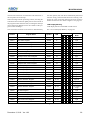
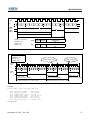
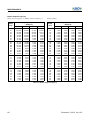
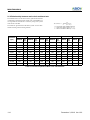
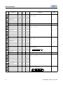
Pin No.
PIN NAME
Secondary
Function
Primary Function
State
@ Reset
State
@ STOP
MC81F8816Q
MC81F8616Q
I/O
Description
I/O
Description
VDD
61
48
-
Supply Voltage
-
-
-
-
VSS
64
51
-
Circuit Ground
-
-
-
-
RESET / R47
67
54
I
General I/O port
I
Reset (low
active)
‘L’ input
‘H’ input
XIN/R45,
XOUT/R46
65,66
52,53
I,O
Main clock oscillator
-
-
Oscillation
‘L’, ‘H’
SXIN/R43,
SXOUT/R44
62,63
49,50
I,O
Sub clock oscillator
-
-
R50/SEG0 ~
R77/SEG23
8~31
3~26
I/O
General I/O port
O
LCD segment
output
Input port
SEG24~SEG25
6,7
1,2
O
LCD segment output
-
-
-
SEG26~SEG27
4,5
63,64
O
LCD segment output
-
-
-
SEG28~SEG35
1~3,76~80
-
O
LCD segment output
-
-
-
SEG36/COM7~
SEG39/COM4
72~75
62~59
O
LCD segment output
O
LCD common
output
Output
port
COM3 ~ COM0
34~37
39~42
O
LCD common output
-
-
-
AVref
56
45
I
Analog Power Voltage Input to A/D
Converter
-
-
-
PLLC
60
47
I
PLL input
-
-
-
R40
57
-
I/O
-
-
R41/INT3
58
-
I/O
I
Interrupt3 Input
R42
49
46
I/O
-
-
General I/O port
Oscillation
State of
before
STOP
Input port
Table 5-1 Port Function Description
14
December 3, 2012 Ver 1.03
MC81F8816/8616
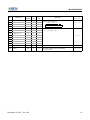
Pin No.
PIN NAME
Secondary
Function
Primary Function
MC81F8816Q
MC81F8616Q
I/O
R00/PWM0/
T0O
32
27
R01/EC0
33
R02
I/O
Description
I/O
O
Timer1 PWM
Output
Timer0 Output
-
I/O
I
Timer0 Event
Counter Input
34
-
I/O
-
-
R03
35
-
I/O
-
-
R04/BUZO
36
28
I/O
O
Buzzer Output
R05/EC1/INT0
37
29
I/O
I
Timer2 Event
Counter Input
Interrupt0 Input
R06/INT1
38
30
I/O
I
Interrupt1 Input
R07/INT2
39
31
I/O
I
Interrupt2 Input
R10/PWM1/
T2O
40
32
I/O
O
Timer3 PWM
Output
Timer2 Output
I/
O
Asynchronous
Serial Interface
Clock Input
/ SIO Serial
Clock
Input/Output
O
UART Serial
Data Output
/ SIO Serial
Data Output
R11/ACK/SCK
R12/TX/SOUT
41
42
33
I/O
34
I/O
Description
General I/O port
R13/RX/SI
43
35
I/O
I
UART Serial
Data Input
/ SIO Serial
Data Input
R14
44
36
I/O
-
-
R15
45
37
I/O
-
-
R16/SDA
46
38
I/O
I/
O
SIO Serial Data
In/Out
R17/SCL
47
39
I/O
I/
O
I2C Serial
Clock In/Out
R20/AN0 ~
R24/AN4
48~52
40~44
I/O
I
A/D Converter
Analog Input
R25/AN5 ~
R27/AN7
53~55
-
I/O
I
A/D Converter
Analog Input
State
@ Reset
State
@ STOP
Input port
State of
before
STOP
Table 5-1 Port Function Description
December 3, 2012 Ver 1.03
15
MC81F8816/8616
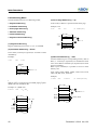
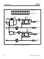
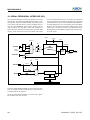
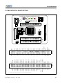
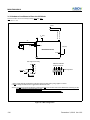
6. PORT STRUCTURES
R01/EC0, R05/EC1/INT0, R06/INT1, R07/INT2, R13/
RX/SI, R16/SDA, R41/IN3
VDD
Pull up Register
Pull-up Tr.
Data Bus
Open Drain Register
VDD
VDD
Data Register
Pin
Direction Register
RD
1
MUX
0
VSS
VSS
0
MUX
1
Noise
Canceller
Sub Func.
Input Register
Sub Func.
Input Enable
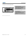
R00/PWM0/T0O, R04/BUZO, R10/PWM1/T2O, R17/
SCL
VDD
Pull-up Tr.
Pull up Register
Data Bus
Open Drain Register
Data Register
Sub Func.
Output Register
VDD
VDD
0
MUX
1
Sub Func.
Output Enable
Pin
RD
Direction Register
VSS
VSS
0
MUX
1
16
December 3, 2012 Ver 1.03
MC81F8816/8616
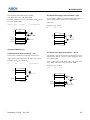
R11/ACK/SCK, R12/TX/SOUT
VDD
Pull-up Tr.
Pull up Register
Data Bus
Open Drain Register
Data Register
Sub Func.
Output Register
VDD
VDD
0
MUX
1
Sub Func.
Output Enable
Pin
1
MUX
0
VSS
VSS
RD
Direction Register
0
MUX
1
Noise
Canceller
Sub Func.
Input Register
Sub Func.
Input Enable
Priority :ACK > SCK(in) > SCK(out)
TX1 > SOUT(out) > SOUT(in)
R20/AN0~R27/AN7
VDD
Pull-up Tr.
Pull up Register
Data Bus
Open Drain Register
VDD
VDD
Data Register
Pin
Direction Register
RD
VSS
VSS
1
MUX
0
ADC Input Data
ADC Enable &
Channel Selectable
December 3, 2012 Ver 1.03
17
MC81F8816/8616
R02, R03, R14, R15, R40, R42
VDD
Pull-up Tr.
Pull up Register
Data Bus
Open Drain Register
VDD
VDD
Data Register
Pin
VSS
VSS
RD
Direction Register
1
MUX
0
R50/SEG0~R77/SEG23
VCL2 or VCL1
LCD Data Registger
Frame Counter
LCD Control
VSS
Data Bus
VDD
VDD
Data Register
Port Selection Register
Pin
RD
Direction Register
VSS
VSS
1
MUX
0
18
December 3, 2012 Ver 1.03
MC81F8816/8616
XIN, XOUT (Crystal or Ceramic resonator)
COM0~COM3
VDD
VCL2 or VCL1
MAIN
CLOCK
VCL2
Frame Counter
XOUT
VSS
Pin
LCD Control
VDD
VSS
VCL0 or VSS
XIN
STOP
COM0~COM3,SEG24~SEG35,COM4/
SEG39~COM7/SEG36
VCL2 or VCL1
VSS
XIN, XOUT (@RC, R)
VCL2
VDD
fXIN ÷ 4
(‘H’ Output@STOP)
LCD Data
Reg.
Frame Counter
XOUT
Pin
LCD Control
VSS
VDD
VSS
VCL0 or VSS
VDD
RESET(R47)
STOP
XIN
VDD
Pull up
Reg.
Pull-up Tr.
Main
Clock
RD
VSS
÷2
Pin
Internal RESET
VSS
IRESET Disable
(Configuration
option bit)
SXIN, SXOUT
VDD
VDD
PLLC
POWER=VREG
VDD
SXIN
Pin
VSS
December 3, 2012 Ver 1.03
SXOUT
VSS
VSS
VSS
LEVEL
SHIFT
DIASBLE
SUB
CLOCK
19
MC81F8816/8616
R43(SXIN), R44(SXOUT)
R45 (XIN), R46 (XOUT)
Pull-up
Tr.
Pull-up
Reg.
Open Drain
Reg.
VDD
Pull-up
Tr.
Pull-up
Reg.
Open Drain
Reg.
VDD
Data Reg.
VDD
VDD
Data Reg.
SXIN
/ R43
Direction
Reg.
VSS
Data Bus
VDD
Direction
Reg.
XIN
/ R45
VSS
VSS
MUX
Data Bus
RD
VSS
MUX
RD
Xinout Disable
(Configuration
option bit)
Disable
Main Clock
(to ONP Block)
VDD
Pull-up
Tr.
Sub Clock
Pull-up
Reg.
Open Drain
Reg.
VDD
Open Drain
Reg.
VDD
Data Reg.
VDD
Data Reg.
Direction
Reg.
SXOUT
/ R44
VSS
Data Bus
VDD
Direction
Reg.
XOUT
/ R46
VSS
MUX
VSS
Data Bus
RD
VSS
MUX
RD
Pull-Up Enable
VDD
20
December 3, 2012 Ver 1.03
MC81F8816/8616
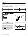
7. ELECTRICAL CHARACTERISTICS
7.1 Absolute Maximum Ratings
Supply voltage ........................................... -0.3 to +6.0 V
Maximum current (ΣIOH)...................................... 80 mA
Supply Voltage (AVref) ............... VDD-0.3 to VDD+0.3 V
Total Power Dissipation (PT) .............................. 600 mW
Storage Temperature ................................-45 to +125 °C
Voltage on any pin with respect to Ground (VSS)
............................................................... -0.3 to VDD+0.3
Maximum current sunk by (IOL per I/O Pin) ........20 mA
Maximum output current sourced by (IOH per I/O Pin)
...............................................................................10 mA
Note: Stresses above those listed under “Absolute Maximum Ratings” may cause permanent damage to the device. This is a stress rating only and functional operation of
the device at any other conditions above those indicated in
the operational sections of this specification is not implied.
Exposure to absolute maximum rating conditions for extended periods may affect device reliability.
Maximum current (ΣIOL) ....................................160 mA
7.2 Recommended Operating Conditions
Parameter
Symbol
Condition
Specifications
Unit
Min.
Typ.
Max.
fMAIN=12MHz
4.5
-
5.5
V
fMAIN=4MHz
2.2
-
5.5
V
VDD=2.2~5.5V
1
-
4.0
VDD=4.5~5.5V
1
-
12.0
fSUB
VDD=3.0~5.5V
-
32.768
-
kHz
Sub Operating Frequency
fSUB
VDD=VDD
-
32.768
-
kHz
Operating Temperature
TOPR
VDD=2.2~5.5V
-40
-
85
°C
VDD=4.5~5.5V
-40
-
85
°C
Supply Voltage
Main Operating Frequency
VDD
fMAIN
December 3, 2012 Ver 1.03
MHz
21
MC81F8816/8616
7.3 DC Electrical Characteristics
(TA= -40~85°C, VDD=2.2~5.5V, VSS=0V)
Parameter
Input High Voltage
Input Low Voltage
Output High Voltage
Output Low Voltage
Symbol
Pin / Condition
Specifications
Min.
Typ.
Max.
VIH1
R0~R7
0.7VDD
-
VDD+0.3
VIH2
RESET, RX0, SI, SCK, ACK, XIN, SXIN,
INT0~3, EC0~1
0.8VDD
-
VDD+0.3
VIL1
R0~R7
-0.3
-
0.3VDD
VIL2
RESET, RX0, SI, SCK, ACK, XIN, SXIN,
INT0~3, EC0~1
-0.3
-
0.2VDD
VOH1
R0~R4 (VDD=4.5V, IOH1=-1.6mA)
VDD-0.3
-
-
VOH2
R5~R7 (VDD=4.5V, IOH2=-1.6mA)
VDD-1.0
-
-
VOH31
SEG0~39, COM0~3
(VDD=4.5V, VCL3~0=3V, IOH3=-15μA)
VCL3-0.4
-
-
VOL1
R0~R4 (VDD=4.5V, IOL1=1.6mA)
-
-
0.35
VOL2
R5~R7 (VDD=4.5V, IOL2=1.6mA)
0.4
VOL32
SEG0~39, COM0~3
(VDD=4.5V, VCL3~0=3V, IOL3=15μA)
0.12
Unit
V
V
V
V
Input High
Leakage Current
IIH
All input pins including R5~R7 (VIN=VDD)
-
-
1
Input Low
Leakage Current
IIL
All input pins including R5~R7 (VIN=Vss)
-1
-
-
VDD (BODR<2:0>=000)
2.0±15%
2.0
2.0±15%
V
VDD (BODR<2:0>=011)
2.7±15%
2.7
2.7±15%
V
VDD (BODR<2:0>=110)
3.6±15%
3.6
3.6±15%
2.4
2.8
V
0.3
V
Brown-out Detector
POR(Power on
Reset) Level
μA
VBOD
VPOR
VDD (TA=25°C)
2.0
VDD Start Voltage3
VSTART
VDD (TA=25°C)
Vss
Config Read
Voltage3
Vconfig
VDD rising Time3
TVDD
VDD (TA=25°C)
Hysteresis
VT+ ~
VT-
RESET, RX0, INT0~3, EC0~1 (VDD=5V)
TVDD=40ms/V, VSTART=VSS
1.8
V
40
ms/V
0.2VDD
-
0.8VDD
V
20
-
60
μA
Pull-up Current
IPU
R0~R4 (VDD=3.0V, VPIN=0V)
Current dissipation in
active mode4
IDD
VDD( fMAIN=12MHz, VDD=5.5V, fSUB=0 )
-
5
15
Current dissipation in
sleep mode5
ISLEEP
VDD ( fMAIN=12MHz, VDD=5.5V, fSUB=0 )
-
2
4
Isubactive fMAIN=off, VDD=5V, fSUB=32.768kHz
-
67
-
μA
Isubsleep
fMAIN=off, VDD=5V, fSUB=32.768kHz
-
32
-
μA
ISTOP
fMAIN=off, VDD=5.5V, fSUB=0
-
3
7
μA
ISUB
fMAIN=off, VDD=5.5V, fSUB=32.768kHz
7
14
μA
8
8±10%
MHz
Current dissipation in
sub active mode6
Current dissipation in
stop mode
Internal 8MHz Oscillation Frequency
22
mA
fIN8M
VDD=5V, TA=25°C
8±10%
December 3, 2012 Ver 1.03
MC81F8816/8616
Parameter
Symbol
Pin / Condition
Internal 4MHz Oscillation Frequency
fIN4M
VDD=5V, TA=25°C
1.
2.
3.
4.
5.
6.
Specifications
Min.
Typ.
Max.
±10%
4
±10%
Unit
MHz
VOH3 is the voltage when VCL3, VCL2, VCL1 and VCL0 are supplied at pads.
VOL3 is the voltage when VSS is supplied at pad.
These parameters are presented for design guidance only and not tested or guaranteed.
Current dissipation is proportioned according to operation voltage and frequency.
In sleep mode, oscillation continues and peripherals are operated normally but internal CPU clock stops.
In sub sleep mode, sub oscillation continues and peripherals are operated normally but internal CPU clock stops.
V
VDD
TVDD ≤ 40ms/V
VDDMIN
Config(POR) Read
Detection Point
Config(POR) Read
Detection Point
VCONFIG
No Config(POR) Read
VSTART
0V
T
Figure 7-1 Config Read Voltage including POR vs Supply Voltage
7.4 LCD Characteristics
(TA= -40~85°C, VDD=2.2~5.5V, VSS=0V)
Parameter
Symbol
LCD Common
Output Current
ICOM
LCD Segment
Output Current
ISEG
Specifications
Condition
Output Voltage Deviation=0.2V
Min.
Typ.
Max.
30
-
-
Unit
μA
Output Voltage Deviation=0.2V
5
−
-
7.5 A/D Converter Characteristics
(TA= -40~85°C, VDD=AVref=5.12V/3.072V, VSS=0V)
Parameter
Symbol
Pin/Condition
NR
Specifications
Min.
Typ.
Max.
-
-
10
-
AVREF1
-
AVSS
-
VDD
Analog Input Voltage Range
VAIN
-
AVSS
-
AVref
Conversion Current
ICON
VDD = 5.12V
FXIN = 8MHz
-
80
200
Resolution
Analog Power Supply Input Voltage Range
December 3, 2012 Ver 1.03
Unit
Bit
V
μA
23
MC81F8816/8616
Parameter
Symbol
Pin/Condition
Overall Accuracy
NACC
-
Non Linearity Error
Specifications
Min.
Typ.
Max.
-
±1.0
±3.0
NNLE
-
-
±3.0
Differential Non Linearity Error
NDNLE
-
-
±3.0
Zero Offset Error
NZOE
-
-
±3.0
Full Scale Error
NFSE
-
-
±3.0
Gain Error
NGE
-
-
±3.0
fXIN = 4MHz
Unit
LSB
Conversion Time (Clock)
TCONV
(TACLK)
Conversion Time
= TACLK x 13
1.0
-
-
μS
Analog Input Impedance
RAN
-
5
100
-
MΩ
1. If the AVREF voltage is less than VDD voltage and anlalog input pins(ANX), shared with various alternate function, are used bidirectional I/
O port, the leakage current may flow VDD pin to AVREF pin in output high mode or anlalog input pins(ANX) to AVREF pin in input high
mode.
24
December 3, 2012 Ver 1.03
MC81F8816/8616
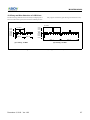
7.6 AC Characteristics
(TA=25°C, VDD=4V, AVref=4V, VSS=AVSS=0V)
Parameter
Symbol
Pins
Main Operating Frequency
fMCP
Sub Operating Frequency
Specifications
Unit
Min.
Typ.
Max.
XIN
0.4
-
12
MHz
fSCP
SXIN
30
32.768
35
kHz
System Clock Frequency1
tSYS
-
166
-
5000
nS
Main Oscillation
Stabilization Time (4MHz)
tMST
XIN, XOUT
-
-
20
mS
Sub Oscillation
Stabilization Time
tSST
SXIN, SXOUT
-
1
2
S
tMCPW
XIN
35
-
-
nS
tSCPW
SXIN
5
-
-
μS
tRCP, tFCP
XIN
-
-
20
nS
tIW
INT0, INT1, INT2, IN3
2
-
-
tSYS
RESET Input Pulse “L” Width
tRST
RESET
8
-
-
tSYS
Event Counter Input
“H” or “L” Pulse Width
tECW
EC0~1
2
-
-
tSYS
tREC, tFEC
EC0~1
-
-
20
nS
External Clock
“H” or “L” Pulse Width
External Clock Transition Time
Interrupt Pulse Width
Event Counter Transition Time
1.SCMR=XXXX000XB that is fMAIN÷2
December 3, 2012 Ver 1.03
25
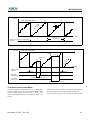
MC81F8816/8616
tMCPW
1/fMCP
tMCPW
0.9VDD
XIN
0.1VDD
tFCP
tRCP
tSYS
tSCPW
1/fSCP
tSCPW
0.9VDD
SXIN
0.1VDD
tIW
tIW
0.8VDD
INT0
INT1
INT2
INT3
0.2VDD
tRST
RESET
0.2VDD
tECW
EC0
EC1
tECW
0.8VDD
0.2VDD
Figure 7-2 AC Timing Chart
26
December 3, 2012 Ver 1.03
MC81F8816/8616
7.7 Serial I/O Characteristics
(TA= -40~85°C, VDD=5.0V±10%, VSS=0V)
Parameter
Symbol
Specifications
Pins
Min.
Typ.
Max.
Input Clock Pulse Period
tSCYC
2tSYS+200
-
-
Input Clock “H” or “L”
Pulse Width
tSCKW
tSYS+70
-
-
tFSCK,tRSCK
-
-
30
4tSYS
-
16tSYS
Input Clock Pulse
Transition Time
SCK
Ouput Clock Cycle Time
tSCYC
Output Clock “H” or “L”
Pulse Width
tSCKW
2tSYS-30
-
-
tFSCK,tRSCK
-
-
30
tDS
-
-
100
tFSIN, tRSIN
-
-
30
Input Setup Time
(External SCK)
tESUS
100
-
-
Input Setup Time
(Internal SCK)
tISUS
200
-
-
Input Hold Time
tHS
tSYS+70
-
-
Output Clock Transition Time
Output Clock Delay Time
Input Pulse Transition Time
Unit
ns
SI
tFSCK
SCLK
tSCYC
tRSCK
tSCKW
0.8VDD
0.2VDD
tSUS
tHS
0.8VDD
0.2VDD
SI
tDS
SO
tSCKW
tFSIN
tRSIN
0.8VDD
0.2VDD
Figure 7-3 Serial I/O Timing Chart
December 3, 2012 Ver 1.03
27
MC81F8816/8616
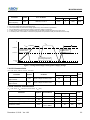
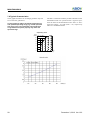
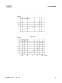
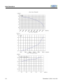
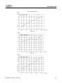
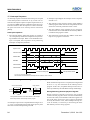
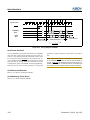
7.8 Typical Characteristics
These graphs and tables are for design guidance only and
are not tested or guaranteed.
The data is a statistical summary of data collected on units
from different lots over a period of time. “Typical” represents the mean of the distribution while “max” or “min”
represents (mean + 3σ) and (mean − 3σ) respectively
where σ is standard deviation.
In some graphs or tables, the data presented are outside specified operating range (e.g. outside specified
VDD range). This is for information only and devices
are guaranteed to operate properly only within the
specified range.
Operating Area
fMAIN
(MHz) Ta= -40~85°C
(Main-clock)
12
10
8
6
4
2
0
28
1
2
3
4
5
VDD
6 (V)
December 3, 2012 Ver 1.03
MC81F8816/8616
December 3, 2012 Ver 1.03
29
MC81F8816/8616
30
December 3, 2012 Ver 1.03
MC81F8816/8616
December 3, 2012 Ver 1.03
31
MC81F8816/8616
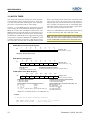
8. MEMORY ORGANIZATION
The have separate address spaces for Program memory,
Data Memory and Display memory. Program memory can
only be read, not written to. It can be up to 16K bytes of
Program memory. Data memory can be read and written to
up to 512 bytes including the stack area. Display memory
has prepared 64bytes for LCD.
8.1 Registers
This device has six registers that are the Program Counter
(PC), a Accumulator (A), two index registers (X, Y), the
Stack Pointer (SP), and the Program Status Word (PSW).
The Program Counter consists of 16-bit register.
A
ACCUMULATOR
X
X REGISTER
Y
Y REGISTER
SP
PCH
STACK POINTER
PCL
PROGRAM COUNTER
PSW
PROGRAM STATUS
WORD
Generally, SP is automatically updated when a subroutine
call is executed or an interrupt is accepted. However, if it
is used in excess of the stack area permitted by the data
memory allocating configuration, the user-processed data
may be lost.
The stack can be located at any position within 100H to
1FFH of the internal data memory. The SP is not initialized
by hardware, requiring to write the initial value (the location with which the use of the stack starts) by using the initialization routine. Normally, the initial value of “1FFH” is
used.
Stack Address (100H ~ 1FFH)
15
8
7
1
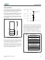
Figure 8-1 Configuration of Registers
Accumulator: The Accumulator is the 8-bit general purpose register, used for data operation such as transfer, temporary saving, and conditional judgement, etc.
The Accumulator can be used as a 16-bit register with Y
Register as shown below.
0
SP
Hardware fixed : RAM 1 page = 01XXH
Caution:
The Stack Pointer must be initialized by software because its value is undefined after RESET.
Example: To initialize the SP
Y
Y
A
A
Two 8-bit Registers can be used as a “YA” 16-bit Register
Figure 8-2 Configuration of YA 16-bit Register
LDX
TXSP
#0FFH
;
;SP ← 0FFH
Program Counter: The Program Counter is a 16-bit wide
which consists of two 8-bit registers, PCH and PCL. This
counter indicates the address of the next instruction to be
executed. In reset state, the program counter has reset routine address (PCH:0FFH, PCL:0FEH).
X, Y Registers: In the addressing mode which uses these
index registers, the register contents are added to the specified address, which becomes the actual address. These
modes are extremely effective for referencing subroutine
tables and memory tables. The index registers also have increment, decrement, comparison and data transfer functions, and they can be used as simple accumulators.
Program Status Word: The Program Status Word (PSW)
contains several bits that reflect the current state of the
CPU. The PSW is described in Figure 8-3. It contains the
Negative flag, the Overflow flag, the Break flag the Half
Carry (for BCD operation), the Interrupt enable flag, the
Zero flag, and the Carry flag.
Stack Pointer: The Stack Pointer is an 8-bit register used
for occurrence interrupts and calling out subroutines. Stack
Pointer identifies the location in the stack to be accessed
(save or restore).
This flag stores any carry or borrow from the ALU of CPU
after an arithmetic operation and is also changed by the
Shift Instruction or Rotate Instruction.
32
[Carry flag C]
December 3, 2012 Ver 1.03
MC81F8816/8616
[Zero flag Z]
This flag is set when the result of an arithmetic operation
or data transfer is “0” and is cleared by any other result.
MSB
PSW
LSB
N V G B H
I
Z C
RESET VALUE : 00H
CARRY FLAG RECEIVES
CARRY OUT
NEGATIVE FLAG
OVERFLOW FLAG
ZERO FLAG
SELECT DIRECT PAGE
when g=1, page is addressed by RPR
INTERRUPT ENABLE FLAG
HALF CARRY FLAG RECEIVES
CARRY OUT FROM BIT 1 OF
ADDITION OPERLANDS
BRK FLAG
Figure 8-3 PSW (Program Status Word) Register
[Interrupt disable flag I]
This flag enables/disables all interrupts except interrupt
caused by Reset or software BRK instruction. All interrupts are disabled when cleared to “0”. This flag immediately becomes “0” when an interrupt is served. It is set by
the EI instruction and cleared by the DI instruction.
[Half carry flag H]
After operation, this is set when there is a carry from bit 3
of ALU or there is no borrow from bit 4 of ALU. This bit
can not be set or cleared except CLRV instruction with
Overflow flag (V).
[Break flag B]
This flag is set by software BRK instruction to distinguish
BRK from TCALL instruction with the same vector address.
the direct addressing mode, addressing area is from zero
page 00H to 0FFH when this flag is "0". If it is set to "1",
addressing area is assigned by RPR register (address
0F3H). It is set by SETG instruction and cleared by CLRG.
[Overflow flag V]
This flag is set to “1” when an overflow occurs as the result
of an arithmetic operation involving signs. An overflow
occurs when the result of an addition or subtraction exceeds +127 (7FH) or −128 (80H). The CLRV instruction
clears the overflow flag. There is no set instruction. When
the BIT instruction is executed, bit 6 of memory is copied
to this flag.
[Negative flag N]
This flag is set to match the sign bit (bit 7) status of the result of a data or arithmetic operation. When the BIT instruction is executed, bit 7 of memory is copied to this flag.
[Direct page flag G]
This flag assigns RAM page for direct addressing mode. In
December 3, 2012 Ver 1.03
33
MC81F8816/8616
At execution of a
CALL/TCALL/PCALL
At acceptance
of interrupt
01FC
01FC
01FD
01FD
PSW
01FE
PCL
01FF
PCH
Push
down
At execution
of RET instruction
01FC
01FC
01FD
Push
down
At execution
of RETI instruction
01FE
PCL
01FF
PCH
01FD
PSW
01FE
PCL
01FF
PCH
01FE
PCL
01FF
PCH
SP before
execution
01FF
01FF
01FD
01FC
SP after
execution
01FD
01FC
01FF
01FF
At execution
of PUSH instruction
PUSH A (X,Y,PSW)
01FC
01FD
01FD
01FF
0100H
01FE
A
Push
down
Pop
up
At execution
of POP instruction
POP A (X,Y,PSW)
01FC
01FE
Pop
up
01FF
A
SP before
execution
01FF
01FE
SP after
execution
01FE
01FF
Pop
up
Stack
depth
01FFH
Figure 8-4 Stack Operation
34
December 3, 2012 Ver 1.03
MC81F8816/8616
8.2 Program Memory
A 16-bit program counter is capable of addressing up to
64K bytes, but this device has 16K bytes program memory
space only physically implemented. Accessing a location
above FFFFH will cause a wrap-around to 0000H.
Figure 8-5 shows a map of Program Memory. After reset,
the CPU begins execution from reset vector which is stored
in address FFFEH and FFFFH as shown in Figure 8-6.
As shown in Figure 8-5, each area is assigned a fixed location in Program Memory. Program Memory area contains
the user program.
16K MTP
C000H
FFC0H
TCALL area
FFDFH
FFE0H
FFFFH
Interrupt
Vector Area
PCALL area
FEFFH
FF00H
Example: Usage of TCALL
LDA
#5
TCALL 0FH
:
:
;
;TABLE CALL ROUTINE
;
FUNC_A: LDA
LRG0
RET
;
FUNC_B: LDA
LRG1
2
RET
;
;TABLE CALL ADD. AREA
;
ORG
0FFC0H
DW
FUNC_A
DW
FUNC_B
Table Call (TCALL) causes the CPU to jump to each
TCALL address, where it commences the execution of the
service routine. The Table Call service area spaces 2-byte
for every TCALL: 0FFC0H for TCALL15, 0FFC2H for
TCALL14, etc., as shown in Figure 8-7.
;TCALL ADDRESS AREA
Any area from 0FF00H to 0FFFFH, if it is not going to be
used, its service location is available as general purpose
Program Memory.
Address
E2
Page Call (PCALL) area contains subroutine program to
reduce program byte length by using 2 bytes PCALL instead of 3 bytes CALL instruction. If it is frequently called,
it is more useful to save program byte length.
1
The interrupt causes the CPU to jump to specific location,
where it commences the execution of the service routine.
The External interrupt 0, for example, is assigned to location 0FFFAH. The interrupt service locations spaces 2-byte
interval: 0FF8H and 0FFF9 H for External Interrupt 1,
0FFFAH and 0FFFBH for External Interrupt 0, etc.
0FFE0H
Figure 8-5 Program Memory Map
;1BYTE INSTRUCTION
;INSTEAD OF 2 BYTES
;NORMAL CALL
E4
E6
E8
EA
EC
EE
Vector Area Memory
Watch Timer interrupt Vector Area
Watch dog timer interrupt Vector
Basic Interval Timer Interrupt Vector Area
AD Converter Interrupt Vector Area
I2C Interrupt Vector Area
Timer/Counter 3 Interrupt Vector Area
Timer/Counter 2 Interrupt Vector Area
Timer/Counter 1 Interrupt Vector Area
Timer/Counter 0 Interrupt Vector Area
SPI Interrupt Vector Area
F2
UART TX0 Interrupt Vector Area
UART RX0 Interrupt Vector Area
F4
F6
F8
FA
FE
External Interrupt 3 Vector Area
External Interrupt 2 Vector Area
External Interrupt 1 Vector Area
External Interrupt 0 Vector Area
Reset Interrupt Vector Area
Figure 8-6 Interrupt Vector Area
December 3, 2012 Ver 1.03
35
MC81F8816/8616
Address
Address
Program Memory
0FFC0H
C1
TCALL 15
C2
C3
C4
C5
C6
C7
C8
C9
CA
CB
CC
CD
CE
CF
PCALL Area Memory
0FF00H
PCALL Area
(256 Bytes)
TCALL 14
TCALL 13
TCALL 12
TCALL 11
TCALL 10
TCALL 9
TCALL 8
D0
D1
D2
D3
D4
D5
D6
D7
D8
D9
DA
DB
DC
DD
DE
DF
0FFFFH
TCALL 7
TCALL 6
TCALL 5
TCALL 4
TCALL 3
TCALL 2
TCALL 1
TCALL 0 / BRK *
NOTE:
* means that the BRK software interrupt is using
same address with TCALL0.
Figure 8-7 PCALL and TCALL Memory Area
PCALL→ rel
TCALL→ n
4F35
4A
PCALL 35H
TCALL 4
4F
4A
01001010
35
~
~
~
~
~
~
0D125H
~
~
NEXT
1
Reverse
PC: 11111111 11010110
FH F H
DH 6 H
0FF00H
0FF35H
0FFFFH
NEXT
3
0FF00H
0FFD6H
25
0FFD7H
D1
2
0FFFFH
36
December 3, 2012 Ver 1.03
MC81F8816/8616
Example: The usage software example of Vector address and the initialize part.
ORG 0FFE0H
; Device : MC81F8816
DW
DW
DW
DW
DW
DW
DW
DW
DW
DW
DW
DW
DW
DW
DW
DW
;
;
;
;
;
;
;
;
;
;
;
;
;
;
;
;
WT_INT
BIT_INT
ADC_I2C_INT
TMR3_INT
TMR2_INT
TMR1_INT
TMR0_INT
SPI
NOT_USED
UART0_INT
EX3_INT
EX2_INT
EX1_INT
EX0_INT
NOT_USED
RESET
Watch Timer / Watch Dog Timer
Basic Interval Timer
AD converter / I2C
Timer-3
Timer-2
Timer-1
Timer-0
SPI
Not used
UART TX0, RX0
INT.3
INT.2
INT.1
INT.0
Not used
Reset
;********************************************
;
MAIN
PROGRAM
*
;********************************************
ORG 0C000H
RESET:
DI
;Disable All Interrupts
CLRG
LDX #0
LDA #0
RAM_CLR1:STA {X}+;Page0 RAM Clear(!0000H->!009FH)
CMPX #090H
BNE RAM_CLR1
LDM RPR,#0000_0001B;Page1 RAM Clear(!0100H->!00FFH)
SETG
LDX #0
LDA #0
RAM_CLR2:STA {X}+
CMPX #060H
BNE RAM_CLR2
CLRG
LDX #0FFH;Stack Pointer Initialize
TXSP
LDM RPR,#0000_0000B;Page0 selection
CALL LCD_CLR;Clear LCD display memory
LDM
LDM
LDM
LDM
:
:
LDM
:
:
R0, #0;Normal Port 0
R0IO,#1000_0010B;Normal Port Direction
R0PU,#1000_0010B;Pull Up Selection Set
R0OD,#0000_0001B;R0 port Open Drain control
SCMR,#1111_0000B;System clock control
December 3, 2012 Ver 1.03
37
MC81F8816/8616
8.3 Data Memory
Figure 8-8 shows the internal Data Memory space available. Data Memory is divided into four groups, a user RAM,
control registers, Stack, and LCD memory.
RPR (RAM Page Selection Register)
ADDRESS: 0CFH
INITIAL VALUE: ----_-001B
0000H
MSB
R/W
USER MEMORY
(144 Bytes)
008FH
0090H
00FFH
0100H
01FFH
0200H
026FH
-
-
-
RPR2 RPR1 RPR0
RPR[2:0] (RAM Page Selection)
PERIPHERAL CONTROL
REGISTERS(112Bytes)
USER MEMORY
(Including Stack Area)
(256 Bytes )
USER MEMORY
(112Bytes)
PAGE1
PAGE2
0460H
LCD DISPLAY MEMORY
(40 Bytes)
PAGE4
0487H
RPR2
RPR1
0
0
0
PAGE 0
0
0
1
PAGE 1
0
1
0
PAGE 2
0
1
1
-
1
0
0
PAGE 4
1
0
1
-
1
1
0
-
1
1
1
-
RPR0 RAM Page Selection
Caution1 : After setting RPR, be sure to execute SETG instruction.
Caution2 : When executing CLRG instruction,
be selected PAGE0 regardless of RPR.
Figure 8-10 RAM Page Selection Register
Figure 8-8 Data Memory Map
User Memory
The MC81F8816/8616 have 256 × 8 bits for the user data
memory (RAM). There are three pages internal RAM.
Page is selected by G-flag and RAM page selection register RPR. When G-flag is cleared to “0”, always page 0 is
selected regardless of RPR value. If G-flag is set to “1”,
page will be selected according to RPR value.
Page 0
RPR=1, G=1
-
LSB
R/W
PAGE0
Unimplemented
RPR=0, G=0
-
R/W
Page 1
Page 2
RPR=2, G=1
Page 4
Control Registers
The control registers are used by the CPU and Peripheral
function blocks for controlling the desired operation of the
device. Therefore these registers contain control and status
bits for the interrupt system, the timer/counters, analog to
digital converters and I/O ports. The control registers are in
address range of 090H to 0FFH.
Note that unoccupied addresses may not be implemented
on the chip. Read accesses to these addresses will in general return random data, and write accesses will have an indeterminate effect.
More detailed informations of each register are explained
in each peripheral section.
RPR=4, G=1
Page 0: 000H~09FH
Page 1: 100H~1FFH
Page 2: 200H~26FH
Note: Write only registers can not be accessed by bit manipulation instruction. Do not use read-modify-write instruction. Use byte manipulation instruction.
Page 4: 460H~487H
Figure 8-9 RAM page configuration
Example; To write at CKCTLR
LDM
CKCTLR,#05H ;Divide ratio ÷8
Stack Area
The stack provides the area where the return address is
saved before a jump is performed during the processing
38
December 3, 2012 Ver 1.03
MC81F8816/8616
routine at the execution of a subroutine call instruction or
the acceptance of an interrupt.
When returning from the processing routine, executing the
subroutine return instruction [RET] restores the contents of
the program counter from the stack; executing the interrupt
return instruction [RETI] restores the contents of the program counter and flags.
The save/restore locations in the stack are determined by
Address
Register Name
the stack pointer (SP). The SP is automatically decreased
after the saving, and increased before the restoring. This
means the value of the SP indicates the stack location
number for the next save. Refer to Figure 8-4 on page 34.
LCD Display Memory
LCD display data area is handled in LCD section.
See "18.3 LCD Display Memory" on page 94.
Symbol
R/W
Initial Value
7 6 5 4 3 2 1 0
Addressing
Mode
0090H
I2C Mode Control Register
I2CMR
R/W
0 0 0 0 1 0 0 0
byte
0091H
I2C Status Register
I2CSR
R
0 0 0 0 0 0 0 0
byte
0092H
I2C Clock Control Register
I2CCR
R/W
1 1 1 1 1 1 1 1
byte
0093H
I2C Pipe and Shift Register
I2CPR
R/W
1 1 1 1 1 1 1 1
byte
0094H
I2C Slave Address Register
I2CAR
R/W
0 0 0 0 0 0 0 0
byte
009AH
PLL Control Register
XPLLCR
R/W
0 0 0 0 0 0 0 0
byte
009BH
PLL Data Register
XPLLDAT
R/W
0 0 0 0 0 0 0 0
byte
009EH
WT Read Data Register
WTRH
R
- 0 0 0 0 0 0 0
byte
00A0H
R0 Open Drain Control Register
R0OD
W
0 0 0 0 0 0 0 0
byte1
00A1H
R1 Open Drain Control Register
R1OD
W
0 0 0 0 0 0 0 0
byte
00A2H
R2Open Drain Control Register
R2OD
W
0 0 0 0 0 0 0 0
byte
00A4H
R4Open Drain Control Register
R4OD
W
0 0 0 0 0 0 0 0
byte
00A5H
R0 Pull-up Register
R0PU
W
0 0 0 0 0 0 0 0
byte
00A6H
R1 Pull-up Register
R1PU
W
0 0 0 0 0 0 0 0
byte
00A7H
R2 Pull-up Register
R2PU
W
0 0 0 0 0 0 0 0
byte
00A9H
R4 Pull-up Register
R4PU
W
0 0 0 0 0 0 0 0
byte
00AAH
Port Selection Register 0
PSR0
W
0 0 0 0 - - 0 0
byte
00ABH
Port Selection Register 1
PSR1
W
- - - - - 0 0 0
byte
00ACH
R5 Port Selection Register
R5PSR
R/W
1 1 1 1 1 1 1 1
byte, bit2
00ADH
R6 Port Selection Register
R6PSR
R/W
1 1 1 1 1 1 1 1
byte, bit
00AEH
R7 Port Selection Register
R7PSR
R/W
1 1 1 1 1 1 1 1
byte, bit
00AFH
R8 Port Selection Register
R8PSR
R/W
1 1 1 1 1 1 1 1
byte, bit(EVA
only)
00B0H
R7 Data Register
R7
R/W
0 0 0 0 0 0 0 0
byte
00B2H
LCD Control Register
LCR
R/W
0 0 0 0 0 0 0 0
byte, bit
00B3H
LCD BIAS Control Register
LBCR
R/W
0 1 1 1 1 0 0 0
byte, bit
00B4H
R7 Direction Register
R7IO
W
0 0 0 0 0 0 0 0
byte
00B6H
SPI Mode Control Register
SPIM
R/W
0 0 0 0 0 0 0 1
byte
00B7H
SPI Data Shift Register
SPIR
R/W
- - - - - - - -
byte
Table 8-1 Control Registers
December 3, 2012 Ver 1.03
39
MC81F8816/8616
Address
Register Name
Symbol
R/W
Initial Value
7 6 5 4 3 2 1 0
Addressing
Mode
00B8H
Asynchronous Serial Mode Register
ASIMR
R/W
0 0 0 0 - 0 0 -
byte, bit
00B9H
Asynchronous Serial Status Register
ASISR
R
- - - - - 0 0 0
byte
00BAH
Baud Rate Generator Control Register
BRGCR
R/W
- 0 0 1 0 0 0 0
byte, bit
Receive Buffer Register
RXBR
R
0 0 0 0 0 0 0 0
byte
Transmit Shift Register
TXSR
W
1 1 1 1 1 1 1 1
byte
00BBH
00C0H
R0 port data register
R0
R/W
0 0 0 0 0 0 0 0
byte, bit
00C1H
R0 Direction Register
R0IO
W
0 0 0 0 0 0 0 0
byte
00C2H
R1 port data register
R1
R/W
0 0 0 0 0 0 0 0
byte, bit
00C3H
R1 Direction Register
R1IO
W
0 0 0 0 0 0 0 0
byte
00C4H
R2 port data register
R2
R/W
0 0 0 0 0 0 0 0
byte, bit
00C5H
R2 Direction Register
R2IO
W
0 0 0 0 0 0 0 0
byte
00C8H
R4 port data register
R4
R/W
0 0 0 0 0 0 0 0
byte, bit
00C9H
R4 Direction Register
R4IO
W
0 0 0 0 0 0 0 0
byte
00CAH
R5 port data register
R5
R/W
0 0 0 0 0 0 0 0
byte, bit
00CBH
R5 Direction Register
R5IO
W
0 0 0 0 0 0 0 0
byte
00CCH
R6 port data register
R6
R/W
0 0 0 0 0 0 0 0
byte, bit
00CDH
R6 Direction Register
R6IO
W
0 0 0 0 0 0 0 0
byte
00CEH
Buzzer Driver Register
BUZR
W
1 1 1 1 1 1 1 1
byte
00CFH
Ram Page Selection Register
RPR
R/W
- - - - - 0 0 1
byte, bit
00D0H
Timer 0 Mode Control Register
TM0
R/W
- - 0 0 0 0 0 0
byte, bit
T0
R
0 0 0 0 0 0 0 0
byte
Timer 0 Data Register
TDR0
W
1 1 1 1 1 1 1 1
byte
Timer 0 Capture Data Register
CDR0
R
0 0 0 0 0 0 0 0
byte
Timer 1 Mode Control Register
TM1
R/W
0 0 0 0 0 0 0 0
byte, bit
TDR1
W
1 1 1 1 1 1 1 1
byte
T1
R
0 0 0 0 0 0 0 0
byte
Timer 1 PWM Duty Register
T1PDR
R/W
1 1 1 1 1 1 1 1
byte
Timer 1 Capture Data Register
CDR1
R
0 0 0 0 0 0 0 0
byte
T1PWHR
R/W
- - - - 0 0 0 0
byte
TM2
R/W
- - 0 0 0 0 0 0
byte, bit
T2
R
0 0 0 0 0 0 0 0
byte
Timer 2 Data Register
TDR2
W
1 1 1 1 1 1 1 1
byte
Timer 2 Capture data Register
CDR2
R
0 0 0 0 0 0 0 0
byte
Timer 3 Mode Control Register
TM3
R/W
0 0 0 0 0 0 0 0
byte, bit
TDR3
W
1 1 1 1 1 1 1 1
byte
T3PPR
W
1 1 1 1 1 1 1 1
byte
Timer 0 Register
00D1H
00D2
00D3H
Timer 1 Data Register
Timer 1 Register
00D4H
00D5H
Timer 1 PWM High Register
00D6H
Timer 2 Mode Control Register
Timer 2 Register
00D7H
00D8H
00D9H
Timer 3 Data Register
Timer 3 PWM Period Register
Table 8-1 Control Registers
40
December 3, 2012 Ver 1.03
MC81F8816/8616
Address
Register Name
00DAH
Addressing
Mode
R
0 0 0 0 0 0 0 0
byte
T3PDR
R/W
0 0 0 0 0 0 0 0
byte, bit
CDR3
R
0 0 0 0 0 0 0 0
byte
T3PWHR
W
- - - - 0 0 0 0
byte
R/W
T3
Timer 3 PWM Duty Register
Timer 3 Capture Data Register
Timer 3 Register
Initial Value
7 6 5 4 3 2 1 0
Symbol
00DBH
Timer 3 PWM High Register
00E2H
10bit A/D Converter Mode Control Register
ADCM3
R/W
0 0 0 0 0 0 0 1
byte, bit
00E3H
10bit A/D Converter Result Register Low
ADCRL
R
Undefined
byte
00E4H
10bit A/D Converter Result Register High
ADCRH
W, R
0 1 0 - - - XX
byte, bit
00E5H
BOD Control Register
BODR
R/W
0 0 0 0 0 0 0 0
byte, bit
BITR
R
Undefined
byte
CKCTLR
W
- - 0 1 0 1 1 1
byte
System Clock Mode Register
SCMR
R/W
- - - - - 0 0 0
byte
Watch Dog Timer Register
WDTR
W
0 1 1 1 1 1 1 1
byte
WDTDR
R
Undefined
byte
Watch Timer Register
WTR
W
0 1 1 1 1 1 1 1
byte
00E9H
Stop & Sleep Mode Control Register
SSCR
W
0 0 0 0 0 0 0 0
byte
00EAH
Watch Timer Mode Register
WTMR
R/W
0 0 - - 0 0 0 0
byte, bit
00F4H
Interrupt Generation Flag Register High
INTFH
R/W
- - - 0 0 0 - -
byte, bit
00F5H
Interrupt Generation Flag Register Low
INTFL
R/W
0 0 - - 0 0 0 0
byte, bit
00F6H
Interrupt Enable Register High
IENH
R/W
- 0 0 0 0 0 - -
byte, bit
00F7H
Interrupt Enable Register Middle
IENM
R/W
0 0 0 0 - - - 0
byte, bit
00F8H
Interrupt Enable Register Low
IENL
R/W
0 0 0 0 0 0 - -
byte, bit
00F9H
Interrupt Request Register High
IRQH
R/W
- 0 0 0 0 0 - -
byte, bit
00FAH
Interrupt Request Register Middle
IRQM
R/W
0 0 0 0 - - - 0
byte, bit
00FBH
Interrupt Request Register Low
IRQL
R/W
0 0 0 0 0 0 - -
byte, bit
00FCH
Interrupt Edge Selection Register
IEDS
R/W
0 0 0 0 0 0 0 0
byte, bit
00E6H
00E7H
00E8H
Basic Interval Timer Register
Clock Control Register
Watch Dog Timer Data Register
Table 8-1 Control Registers
1. “byte”, “bit” means that register can be addressed by not only bit but byte manipulation instruction.
2. “byte” means that register can be addressed by only byte manipulation instruction. On the other hand, do not use any read-modify-write
instruction such as bit manipulation.
3. bit 0 of ADCM is read only.
December 3, 2012 Ver 1.03
41
MC81F8816/8616
8.4 Addressing Mode
The MC81F8816/8616 use six addressing modes;
(3) Direct Page Addressing → dp
• Register addressing
In this mode, a address is specified within direct page.
• Immediate addressing
Example; G=0
• Direct page addressing
C535
LDA
;A ←RAM[35H]
35H
• Absolute addressing
• Indexed addressing
35H
• Register-indirect addressing
data
2
~
~
(1) Register Addressing
Register addressing accesses the A, X, Y, C and PSW.
~
~
0E550H
C5
0E551H
35
1
data → A
(2) Immediate Addressing → #imm
In this mode, second byte (operand) is accessed as a data
immediately.
(4) Absolute Addressing → !abs
Example:
0435
ADC
#35H
MEMORY
04
A+35H+C → A
35
Absolute addressing sets corresponding memory data to
Data, i.e. second byte (Operand I) of command becomes
lower level address and third byte (Operand II) becomes
upper level address.
With 3 bytes command, it is possible to access to whole
memory area.
ADC, AND, CMP, CMPX, CMPY, EOR, LDA, LDX,
LDY, OR, SBC, STA, STX, STY
Example;
0735F0
ADC
When G-flag is 1, then RAM address is defined by 16-bit
address which is composed of 8-bit RAM paging register
(RPR) and 8-bit immediate data.
Example: G=1, RPR=01H
E45535
LDM
~
~
0F100H
data
0135H
1
0F100H
42
~
~
data
0F035H
35H,#55H
data ← 55H
;A ←ROM[0F035H]
!0F035H
2
~
~
1
A+data+C → A
07
0F101H
35
0F102H
F0
address: 0F035
~
~
E4
0F101H
55
0F102H
35
December 3, 2012 Ver 1.03
MC81F8816/8616
The operation within data memory (RAM)
ASL, BIT, DEC, INC, LSR, ROL, ROR
Example; Addressing accesses the address 0135H regardless of G-flag and RPR.
981501
INC
;A ←ROM[115H]
!0115H
X indexed direct page, auto increment→ {X}+
In this mode, a address is specified within direct page by
the X register and the content of X is increased by 1.
LDA, STA
Example; G=0, X=35H
DB
data
115H
~
~
98
0F101H
15
0F102H
01
{X}+
3
~
~
0F100H
LDA
2
35H
data+1 → data
~
~
1
2
data
data → A
~
~
1
address: 0115
36H → X
DB
(5) Indexed Addressing
X indexed direct page (no offset) → {X}
X indexed direct page (8 bit offset) → dp+X
In this mode, a address is specified by the X register.
This address value is the second byte (Operand) of command plus the data of X-register. And it assigns the memory in Direct page.
ADC, AND, CMP, EOR, LDA, OR, SBC, STA, XMA
Example; X=15H, G=1, RPR=01H
D4
LDA
{X}
;ACC←RAM[X].
ADC, AND, CMP, EOR, LDA, LDY, OR, SBC, STA
STY, XMA, ASL, DEC, INC, LSR, ROL, ROR
Example; G=0, X=0F5H
C645
115H
data
~
~
0E550H
LDA
45H+X
2
~
~
data → A
1
3AH
data
3
D4
December 3, 2012 Ver 1.03
~
~
~
~
0E550H
C6
0E551H
45
2
data → A
1
45H+0F5H=13AH
43
MC81F8816/8616
Y indexed direct page (8 bit offset) → dp+Y
3F35
JMP
[35H]
This address value is the second byte (Operand) of command plus the data of Y-register, which assigns Memory in
Direct page.
This is same with above. Use Y register instead of X.
35H
0A
36H
E3
Y indexed absolute → !abs+Y
~
~
Sets the value of 16-bit absolute address plus Y-register
data as Memory. This addressing mode can specify memory in whole area.
Example; Y=55H
D500FA
LDA
~
~
0FA00H
0F100H
D5
00
0F102H
FA
~
~
2
jump to address 0E30AH
NEXT
~
~
1
3F
35
!0FA00H+Y
0F101H
0FA55H
0E30AH
~
~
1
0FA00H+55H=0FA55H
~
~
2
data
3
data → A
X indexed indirect → [dp+X]
Processes memory data as Data, assigned by 16-bit pair
memory which is determined by pair data
[dp+X+1][dp+X] Operand plus X-register data in Direct
page.
ADC, AND, CMP, EOR, LDA, OR, SBC, STA
Example; G=0, X=10H
1625
ADC
[25H+X]
(6) Indirect Addressing
Direct page indirect → [dp]
Assigns data address to use for accomplishing command
which sets memory data (or pair memory) by Operand.
Also index can be used with Index register X,Y.
JMP, CALL
35H
05
36H
E0
~
~
0E005H
~
~
0FA00H
25 + X(10) = 35H
~
~
16
25
44
0E005H
1
data
~
~
Example; G=0
2
3
A + data + C → A
December 3, 2012 Ver 1.03
MC81F8816/8616
Y indexed indirect → [dp]+Y
Absolute indirect → [!abs]
Processes memory data as Data, assigned by the data
[dp+1][dp] of 16-bit pair memory paired by Operand in Direct page plus Y-register data.
The program jumps to address specified by 16-bit absolute
address.
ADC, AND, CMP, EOR, LDA, OR, SBC, STA
Example; G=0, Y=10H
1725
ADC
JMP
Example; G=0
1F25E0
JMP
[!0E025H]
[25H]+Y
PROGRAM MEMORY
25H
26H
05
0E025H
25
E0
0E026H
E7
~
~
0E015H
~
~
data
~
~
0FA00H
2
0E005H + Y(10) = 0E015H
1
1
0E725H
0FA00H
17
December 3, 2012 Ver 1.03
3
jump to
address 0E725H
NEXT
~
~
~
~
25
2
~
~
~
~
~
~
1F
25
A + data + C → A
E0
45
MC81F8816/8616
9. I/O PORTS
The MC81F8816/8616 have seven I/O ports, LCD segment ports (R0, R1, R2, R4, R50/SEG00 ~ R77/SEG23,
SEG24 ~ SEG35) and LCD common ports (SEG39/COM4
~ SEG36/COM7, COM0~COM3).
function for the peripheral features on the device.
Note: SEG28 ~ SEG35 are not not supported in
MC81F8616Q(64pin).
These ports pins may be multiplexed with an alternate
9.1 Registers for Ports
Port Data Registers
The Port Data Registers are represented as a D-Type flipflop, which will clock in a value from the internal bus in response to a “write to data register” signal from the CPU.
The Q output of the flip-flop is placed on the internal bus
in response to a “read data register” signal from the CPU.
The level of the port pin itself is placed on the internal bus
in response to “read data register” signal from the CPU.
Some instructions that read a port activating the “read register” signal, and others activating the “read pin” signal.
Port Direction Registers
All pins have data direction registers which can define
these ports as output or input. A “1” in the port direction
register configure the corresponding port pin as output.
Conversely, write “0” to the corresponding bit to specify it
as input pin. For example, to use the even numbered bit of
R0 as output ports and the odd numbered bits as input
ports, write “55H” to address 0C1H (R0 port direction register) during initial setting as shown in Figure 9-1.
All the port direction registers in the MC81F8816/8616
have 0 written to them by reset function. Therefore, its initial status is input.
pull-up port. It is connected or disconnected by Pull-up
Control register (RnPU). The value of that resistor is typically 100kΩ. Refer to DC characteristics for more details.
When a port is used as key input, input logic is firmly either low or high, therefore external pull-down or pull-up
resisters are required practically. The MC81F8816/8616
have internal pull-up, it can be logic high by pull-up that
can be able to configure either connect or disconnect individually by pull-up control registers RnPU.
When ports are configured as inputs and pull-up resistor is
selected by software, they are pulled to high.
VDD
VDD
PULL-UP RESISTOR
PORT PIN
GND
Pull-up control bit
0: Disconnect
1: Connect
Figure 9-2 Pull-up Port Structure
WRITE “55H” TO PORT R0 DIRECTION REGISTER
0C0H
R0 DATA
0C1H
R0 DIRECTION
~
~
0 1 0 1 0 1 0 1
7 6 5 4 3 2 1 0
BIT
~
~
0CCH
R6 DATA
0CDH
R7 DIRECTION
I O
I O I O I O PORT
Open drain port Registers
The R0, R1, R2 and R4 ports have open drain port resistors
R0OD~R4OD.
Figure 9-3 shows an open drain port configuration by control register. It is selected as either push-pull port or opendrain port by R0OD, R1OD, R2OD and R4OD.
7 6 5 4 3 2 1 0
PORT PIN
I : INPUT PORT
O : OUTPUT PORT
Figure 9-1 Example of port I/O assignment
GND
Open drain port selection bit
0: Push-pull
1: Open drain
Pull-up Control Registers
The R0, R1, R2 and R4 ports have internal pull-up resistors. Figure 9-2 shows a functional diagram of a typical
46
Figure 9-3 Open-drain Port Structure
December 3, 2012 Ver 1.03
MC81F8816/8616
9.2 I/O Ports Configuration
R0 Port
R0 is a 8-bit CMOS bidirectional I/O port (address 0C0H).
Each I/O pin can independently used as an input or an output through the R0IO register (address 0C1H).
R0 has internal pull-ups that is independently connected or
disconnected by R0PU. The control registers for R0 are
shown below.
In addition, Port R0 is multiplexed with various special
features. The control register PSR0 (address 0AAH) controls the selection of alternate function. After reset, this
value is “0”, port may be used as normal I/O port.
To use alternate function such as External Interrupt rather
than normal I/O, write “1” in the corresponding bit of
PSR0.
R07
R06
R05
R03
R04
R0 Direction Register
R02
R01
R00
ADDRESS : 0C1H
RESET VALUE : 00000000B
R0IO
Port Direction
0: Input
1: Output
R0 Pull-up
Selection Register
ADDRESS :0A5H
RESET VALUE : 00000000B
R0PU
Pull-up select
0: Without pull-up
1: With pull-up
R0 Open Drain
Selection Register
ADDRESS :0A0H
RESET VALUE : 00000000B
R0OD
Open Drain select
0: No Open Drain
1: Open Drain
Port
Selection Register 0
PSR0
INT1
INT0
R00
R01
R04
R05
R06
R07
Alternate function
PWM0/T0O
(Timer1 PWM Output / Timer0 Output)
EC0 (Timer 0 Event Count Input)
BUZO (Buzzer Output)
EC1 / INT0
(Timer2 Event Count Input/External Interrupt 0 Request Input)
INT1 (External Interrupt 1 Request Input)
INT2 (External Interrupt 2 Request Input)
Note: R0IO, R0PU, P0OD and PSR0 are write-only registers. They can not be read and can not be accessed by bit
manipulation instruction. Do not use read or read-modifywrite instruction. Use byte manipulation instruction.
ADDRESS : 0C0H
RESET VALUE : 00000000B
R0 Data Register
R0
Port pin
ADDRESS :0AAH
RESET VALUE : 0000--00B
EC1 BUZO
-
-
EC0 PWM0O
INT1 (External Interrupt 1)
0: R06 Port
1: INT1 input Port
INT0 (External Interrupt 0)
0: R05 Port
1: INT0 input Port
EC1I (Timer2 Event Input)
0: R05 Port
1: EC1 input Port
BUZO (Buzzer Output)
0: R04 Port
1: BUZO
EC0I (Timer0 Event Input)
0: R01 Port
1: EC0 input Port
PWM0O (PWM0 Output)
0: R00 Port
1: PWM0/T0O
December 3, 2012 Ver 1.03
R1 Ports
R1 is an 8-bit CMOS bidirectional I/O port (address
0C2H). Each I/O pin can independently used as an input or
an output through the R1IO register (address 0C3H).
R1 has internal pull-up that is independently connected or
disconnected by register R1PU. The control registers for
R1 are shown below.
In addition, Port R1 is multiplexed with various special
features. The control register PSR1 (address 0ABH) controls the selection of alternate function. After reset, this
value is “0”, port may be used as normal I/O port.
To use alternate function such as External Interrupt rather
than normal I/O, write “1” in the corresponding bit of
PSR1.
Note: R1IO, R1PU, P1OD and PSR1 are write-only registers. They can not be read and can not be accessed by bit
manipulation instruction. Do not use read or read-modifywrite instruction. Use byte manipulation instruction.
47
MC81F8816/8616
ADDRESS : 0C2H
RESET VALUE : 00000000B
R1 Data Register
R1
R17
R16
R15
R14
R13
R12
R11
R10
ADDRESS : 0C3H
RESET VALUE : 00000000B
R1 Direction Register
nipulation instruction. Do not use read or read-modify-write
instruction. Use byte manipulation instruction.
Note: The R25 and R27 are not supported in the
MC81F8616Q.
R1IO
Port Direction
0: Input
1: Output
R1 Pull-up
Selection Register
ADDRESS : 0A6H
RESET VALUE : 00000000B
R2
R27
R26 R25
R24
R2 Direction Register
R1PU
Pull-up select
0: Without pull-up
1: With pull-up
R1 Open Drain
Selection Register
ADDRESS :0A1H
RESET VALUE : 00000000B
R1OD
Open Drain select
0: No Open Drain
1: Open Drain
Port
Selection Register 1
PSR1
ADDRESS: 0C4H
RESET VALUE: 00000000B
R2 Data Register
-
-
-
INT3 (External Interrupt 3)
0: R41 Port
1: INT3 input Port
-
INT3 INT2 PWM1
INT2 (External Interrupt 2)
0: R07 Port
1: INT2 input Port
PWM1O (PWM1 Output)
0: R10 Port
1: PWM1O/T2O
R22
R21
R20
ADDRESS : 0C5H
RESET VALUE : 00000000B
R2IO
Port Direction
0: Input
1: Output
R2 Pull-up
Selection Register
ADDRESS : 0A7H
RESET VALUE : 00000000B
R2PU
Pull-up select
0: Without pull-up
1: With pull-up
ADDRESS :0ABH
RESET VALUE : -----000B
-
R23
R2 Open Drain
Selection Register
ADDRESS : 0A2H
RESET VALUE : 00000000B
R2OD
Open Drain select
0: No Open Drain
1: Open Drain
A/D Converter
Mode Register
ADDRESS : 0E2H
RESET VALUE : 00000001B
ADCM ADEN ADCK ADS3 ADS2 ADS1 ADS0 ADST ADF
Analog input of A/D
converter is selected
by ADS0~ADS2
R2 Ports
R2 is a 8/5-bit CMOS bidirectional I/O port (address
0C4H). Each I/O pin can independently used as an input or
an output through the R2IO register (address 0C5H).
R2 has internal pull-ups that are independently connected
or disconnected by R2PU (address 0A7H). The control registers for R2 are shown as below.
Note: R2IO, R2PU and P2OD are write-only registers.
They can not be read and can not be accessed by bit ma-
48
R4 Port
R4 is a 8-bit CMOS bidirectional I/O port (address 0C8H).
Each I/O pin can independently used as an input or an output through the R4IO register (address 0C9H).
R4 has internal pull-ups that is independently connected or
disconnected by R4PU. The control registers for R4 are
shown below.
December 3, 2012 Ver 1.03
MC81F8816/8616
writing “1” to the SCKD bit of the LCR register
ADDRESS : 0C8H
RESET VALUE : -0000000B
R4 Data Register
R47
R4
R46
R45
R44
R43
R42
R41
ADDRESS : 0C9H
RESET VALUE : -0000000B
R4 Direction Register
R4IO
Port Direction
0: Input
1: Output
R4 Pull-up
Selection Register
Port pin
Alternate function
R40
R41
R42
R43
R44
R45
R46
R47
INT3 (External Interrupt 3 Request input)
SXIN
SXOUT
XIN
XOUT
RESET
R40
ADDRESS :0A9H
RESET VALUE : 00000000B
R4PU
Pull-up select
0: Without pull-up
1: With pull-up
R4 Open Drain
Selection Register
ADDRESS :0A4H
RESET VALUE : -0000000B
Note: R4IO, R4PU, P4OD and PSR1 are write-only registers. They can not be read and can not be accessed by bit
manipulation instruction. Do not use read or read-modifywrite instruction. Use byte manipulation instruction.
R0OD
Open Drain select
0: No Open Drain
1: Open Drain
Port
Selection Register 1
PSR1
-
-
-
ADDRESS :0ABH
RESET VALUE : -----000B
-
INT3 (External Interrupt 3)
0: R41 Port
1: INT3 input Port
INT3 INT2 PWM1
-
INT2 (External Interrupt 2)
0: R07 Port
1: INT2 input Port
R5 Ports
R5 is an 8-bit CMOS bidirectional I/O port (address
0CAH). Each I/O pin can independently used as an input or
an output through the R5IO register (address 0CBH).
R5 is multiplexed with LCD segment output(SEG0 ~
SEG7), which can be selected by writing appropriate value
into the R5PSR(address 0ACH).
PWM1O (PWM1 Output)
0: R10 Port
1: PWM1O/T2O
ADDRESS :0B2H
RESET VALUE : 00000000B
LCD Control Register
LCR
SCKD
1
LCDEN
0
1
LCDD0 LCK1
LCK0
SCKD (Sub Clock Disable)
0: Sub Clock Oscillation Enable (SXIN/SXOUT)
1: Sub Clock Oscillation Disable(R43/R44)
In addition, Port R4 is multiplexed with oscillation input/
output, reset and interrupt input pins. The control register
PSR1 (address 0ABH) controls the selection of alternate
function. After reset, this value is “0”, port may be used as
normal I/O port. To use alternate function such as External
Interrupt rather than normal I/O, write “1” in the corresponding bit of PSR1.
Main oscillation input/output and reset pin can be used as
normal I/O ports (R46/R45) and normal input port(R47) by
selecting configuration options in flash writing. Sub oscillation input/output pin can be used as normal I/O ports by
ADDRESS: 0CAH
RESET VALUE: 00000000B
R5 Data Register
R5
R57
R56
R55
R54
R53
R5 Direction Register
R52
R51
R50
ADDRESS : 0CBH
RESET VALUE : 00000000B
R5IO
R5/LCD Port
Selection Register
R5PSR
Port Direction
0: Input
1: Output
ADDRESS : 0ACH
RESET VALUE : 11111111B
R5PS7 R5PS6 R5PS5 R5PS4 R5PS3 R5PS2 R5PS1 R5PS0
0: Seg Selection(seg7~seg0)
1: Port Selection
Note: R5IO is write-only register. It can not be read and
can not be accessed by bit manipulation instruction. Do not
use read or read-modify-write instruction. Use byte manipulation instruction.
R6 Ports
R6 is an 8-bit CMOS bidirectional I/O port (address
0CCH). Each I/O pin can independently used as an input or
December 3, 2012 Ver 1.03
49
MC81F8816/8616
an output through the R6IO register (address 0CDH).
R6 is multiplexed with LCD segment output(SEG8 ~
SEG15), which can be selected by writing appropriate value into the R6PSR(address 0ADH).
R7
R67
R66
R65
R77
R76
R75
R74 R73
R72
R71
R70
ADDRESS: 0CCH
RESET VALUE: 00000000B
R6 Data Register
R6
ADDRESS: 0B0H
RESET VALUE: 00000000B
R7 Data Register
R64
R63
R62
R61
R60
R7 Direction Register
ADDRESS : 0B4H
RESET VALUE : 00000000B
R7IO
R6 Direction Register
ADDRESS : 0CDH
RESET VALUE : 00000000B
Port Direction
0: Input
1: Output
R6IO
Port Direction
0: Input
1: Output
R6/LCD Port
Selection Register
R6PSR
ADDRESS : 0ADH
RESET VALUE : 11111111B
R7/LCD Port
Selection Register
R7PSR
ADDRESS : 0AEH
RESET VALUE : 11111111B
R7PS7 R7PS6 R7PS5 R7PS4 R7PS3 R7PS2 R7PS1 R7PS0
0: Seg Selection(seg16~seg23)
1: Port Selection
R6PS7 R6PS6 R6PS5 R6PS4 R6PS3 R6PS2 R6PS1 R6PS0
0: Seg Selection(seg15~seg8)
1: Port Selection
Note: R6IO is write-only register. It can not be read and
can not be accessed by bit manipulation instruction. Do not
use read or read-modify-write instruction. Use byte manipulation instruction.
Note: R7IO is write-only register. It can not be read and
can not be accessed by bit manipulation instruction. Do not
use read or read-modify-write instruction. Use byte manipulation instruction.
SEG0~SEG35
R7 Ports
R7 is a 8-bit CMOS bidirectional I/O port (address 0B0H).
Each I/O pin can independently used as an input or an output through the R7IO register (address 0B4H).
R7 is multiplexed with LCD segment output(SEG16 ~
SEG23), which can be selected by writing appropriate value into the R7PSR(address 0AEH).
Segment signal output pins for the LCD display. See "18.
LCD DRIVER" on page 88 for details.
SEG24 ~ SEG31 is multiplexed with normal I/O port(EVA
chip), which can be selected by writing appropriate value
into the R8PSR(address 0AFH).
COM0~COM7
Common signal output pins for the LCD display. See "18.
LCD DRIVER" on page 88 for details.
SEG36~SEG39 and COM7~COM4 are selected by LCDD
of the LCR register.
50
December 3, 2012 Ver 1.03
MC81F8816/8616
10. CLOCK GENERATOR
The internal system clock should be selected to main oscillation by setting bit1 and bit0 of the system clock mode
register (SCMR). The registers are shown in Figure 10-2.
As shown in Figure 10-1, the clock generator produces the
basic clock pulses which provide the system clock to be
supplied to the CPU and the peripheral hardware. It contains two oscillators which are main-frequency clock oscillator and a sub-frequency clock oscillator.The system
clock can also be obtained from the external oscillator.
By setting configuration option, the internal 8MHz, 4MHz
can also be selected for system clock source.
To the peripheral block, the clock among the not-divided
original clocks, divided by 2, 4,..., up to 4096 can be provided. Peripheral clock is enabled or disabled by STOP instruction. The peripheral clock is controlled by clock
control register (CKCTLR). See "11. BASIC INTERVAL
TIMER" on page 53 for details.
The clock generator produces the system clocks forming
clock pulse, which are supplied to the CPU and the peripheral hardware.
FXTS
(XPLLCR[1])
sub_clk
SXIN
OSC_32K
0
1
PLL
XPLLE
(XPLLCR[0])
XT_EN
(LCR[7])
SCMR
(CS[1:0])
1/2
0
CONFIG[1:0]
(configuration option)
Internal
8MHz
Internal System Clock
1
0
Internal
4MHz
X2EN
(CONFIG[2])
1
OSC
CIRCUIT
XIN
PRESCALER
PS1
PS0
÷1
÷2
PS2
÷4
PS3
÷8
PS4
÷16
PS5
÷32
PS6
÷64
PS7
÷128
PS8
÷256
PS9
PS10
PS11
PS12
÷512 ÷1024 ÷2048 ÷4096
Peripheral clock
fMAIN(Hz)
4M
PS0
PS1
PS2
PS3
PS4
PS5
PS6
PS7
PS8
PS9
PS10
PS11
Frequency
4M
2M
1M
500K
250K
125K
62.5K
31.25K
15.63K
7.183K
3.906K
1.953K
976
period
250n
500n
1u
2u
4u
8u
16u
32u
64u
128u
256u
512u
1.024m
PS12
Figure 10-1 Block Diagram of Clock Generator
December 3, 2012 Ver 1.03
51
MC81F8816/8616
The SCMR should be set to operate by main oscillation.
Bit2, bit1 and bit0 of the SCMR should be set to “000” or
“001” to select main oscillation.
SCMR (System Clock Mode Register)
MSB
LSB
R/W R/W R/W
MCC CS1 CS0
ADDRESS: 0E7H
INITIAL VALUE: -----000B
CS[1:0] (CPU clock selection)
00: main clock
01: main clock
10: sub clock(fsub)
11: Setting prohibited
MCC (Main Clock Oscillation Control)
0: main clock oscillation possible
1: main clock oscillation stopped
Figure 10-2 SCMR System Clock Mode Register
52
December 3, 2012 Ver 1.03
MC81F8816/8616
11. BASIC INTERVAL TIMER
The MC81F8816/8616 have one 8-bit Basic Interval Timer
that is free-run and can not stop. Block diagram is shown
in Figure 11-1.
interrupt to be generated. The Basic Interval Timer is controlled by the clock control register (CKCTLR) shown in
Figure 11-2.
The Basic Interval Timer Register (BITR) is increased every internal count pulse which is divided by prescaler.
Since prescaler has division ratio from 8 to 1024, the count
rate is 1/8 to 1/1024 of the oscillator frequency. After reset,
the BCK bits are all set, so the longest oscillation stabilization time is obtained.
Source clock can be selected by lower 3 bits of CKCTLR.
When write “1” to bit BCL of CKCTLR, BITR register is
cleared to “0” and restart to count up. The bit BCL becomes “0” automatically after one machine cycle by hardware.
BITR and CKCTLR are located at same address, and address 0E6H is read as a BITR, and written to CKCTLR.
It also provides a Basic interval timer interrupt (BITF).
The count overflow of BITR from FFH to 00H causes the
fSUB
fMAIN÷23
fMAIN÷24
fMAIN÷25
fMAIN÷2
fMAIN÷27
fMAIN÷28
8-bit up-counter
1
MUX
source
clock
fMAIN÷29
fMAIN÷210
overflow
BITR
0
BITIF
Basic Interval Timer Interrupt
[0E6H]
SELSUB
clear
3
Select Input clock
BCK<2:0>
fMAIN: main-clock frequency
fSUB: sub-clock frequency
[0E6H]
BCL
CKCTLR
Basic Interval Timer
clock control register
Internal bus line
Figure 11-1 Block Diagram of Basic Interval Timer
BCK<2:0>
000
001
010
011
100
101
110
111
Source clock
Interrupt (overflow) Period
SCMR[1:0] = 00 or 01
At fMAIN = 4MHz
fMAIN÷23
fMAIN÷24
fMAIN÷25
fMAIN÷26
fMAIN÷27
fMAIN÷28
fMAIN÷29
fMAIN÷210
0.512 ms
1.024
2.048
4.096
8.192
16.384
32.768
65.536
Table 11-1 Basic Interval Timer Interrupt Time
December 3, 2012 Ver 1.03
53
MC81F8816/8616
W
6
7
CKCTLR
-
W
5
W
4
W
3
W
2
W
1
W
0
ADRST SELSUB WDTON BCL BCK2 BCK1 BCK0
Address Trap Reset Selection
0 : Enable Adress Fail Reset
1 : Disable Adress Fail Reset
ADDRESS: 0E6H
INITIAL VALUE: -0010111B
Basic Interval Timer source clock select
000: fMAIN÷23
001: fMAIN÷24
fMAIN: main-clock frequency
010: fMAIN÷25
011: fMAIN÷26
100: fMAIN÷27
101: fMAIN÷28
110: fMAIN÷29
111: fMAIN÷210
SUB Clock Selection
0 : Deselect Sub Clock
1 : Select Sub Clock
Watch Dog Timer Enable
0 : Operates as a 7-bit Timer
1 : Enable Watchdog Timer
Clear bit
0: Normal operation (free-run)
1: Clear 8-bit counter (BITR) to "0". This bit becomes 0 automatically
after one machine cycle.
Caution:
Both register are in same address,
when write, to be a CKCTLR,
when read, to be a BITR.
R
7
R
6
R
5
R
4
R
3
R
2
BITR
R
1
R
0
ADDRESS: 0E6H
INITIAL VALUE: 00H
8-BIT BINARY COUNTER
Figure 11-2 BITR: Basic Interval Timer Mode Register
Example 1:
Interrupt request flag is generated every 8.192ms at 4MHz.
:
LDM
SET1
EI
:
54
CKCTLR,#0CH
BITE
December 3, 2012 Ver 1.03
MC81F8816/8616
12. TIMER / COUNTER
Timer/Event Counter consists of prescaler, multiplexer, 8bit timer data register, 8-bit counter register, mode register,
input capture register and Comparator as shown in Figure
12-4. And the PWM high register for PWM is consisted
separately.
The timer/counter has seven operating modes.
- 8 Bit Timer/Counter Mode
- 8 Bit Capture Mode
- 8 Bit Compare Output Mode
- 16 Bit Timer/Counter Mode
- 16 Bit Capture Mode
- 16 Bit Compare Output Mode
- PWM Mode
In the “timer” function, the register is increased every internal clock input. Thus, one can think of it as counting internal clock input. Since a least clock consists of 2 and
most clock consists of 2048 oscillator periods, the count
rate is 1/2 to 1/2048 of the oscillator frequency in Timer0.
And Timer1 can use the same clock source too. In addition,
Timer1 has more fast clock source (1/1 to 1/8).
In the “counter” function, the register is increased in response to a 0-to-1 (rising edge) transition at its corresponding external input pin EC0 (Timer 0).
In addition the “capture” function, the register is increased
in response external or internal clock interrupt same with
timer/counter function. When external interrupt edge input, the count register is captured into capture data register
TMx.
Timer3 is shared with “PWM” function and Timer2 is
shared with “Compare output” function.
Example 1:
Example 3:
Timer 0 = 8-bit timer mode, 8ms interval at 4MHz
Timer 1 = 8-bit timer mode, 4ms interval at 4MHz
Timer0 = 8-bit event counter
LDM
LDM
LDM
LDM
LDM
SCMR,#0
;Main clock mode
TDR0,#249
TM0,#0001_0011B
TDR1,#124
TM1,#0000_1111B
SET1
SET1
EI
:
:
:
T0E
T1E
Timer2 = 8-bit capture mode, 2us sampling count.
LDM
LDM
LDM
TDR0,#0FFH
TM0,#1FH
R0IO,#1XXX_XX1XB
;don’t care
;event counter
;R07, R01 input
LDM
LDM
LDM
LDM
IEDS,#XXXX_01XXB
PSR0,#1XXX_XX1XB
TDR2,#0FFH
TM2,#0010_1011B
;FALLING
;INT1,EC0
SET1
SET1
SET1
EI
:
T0E
T2E
INT1E
;ENABLE TIMER 0
;ENABLE TIMER 1
;ENABLE INT1
;2us
X: don’t care.
Example 2:
Example 4:
Timer0 = 16-bit timer mode, 0.5s at 4MHz
LDM
LDM
LDM
LDM
LDM
SCMR,#0
TDR0,#23H
TDR1,#0F4H
TM0,#0FH
TM1,#4CH
SET1
EI
:
:
:
T0E
;Main clock mode
;FMAIN/32, 8us
Timer0 = 16-bit capture mode, 8us sampling count. at 4MHz
LDM
LDM
LDM
LDM
TDR0,#0FFH
TDR1,#0FFH
TM0,#2FH
TM1,#5FH
LDM
LDM
IEDS,#XXXX_XX01B
PSR0,#X1XX_XXXXB
;AS INT0
SET1
SET1
EI
:
T0E
INT0E
;ENABLE TIMER 0
;ENABLE EXT. INT0
X: don’t care.
December 3, 2012 Ver 1.03
55
MC81F8816/8616
TM0, TM2 (Timer0, 2 Mode Control Register)
Bit :
TM0
Bit :
TM2
7
6
R/W
5
R/W
4
R/W
3
R/W
2
R/W
1
R/W
0
-
-
CAP0
T0CK2
T0CK1
T0CK0
T0CN
T0ST
7
6
R/W
5
R/W
4
R/W
3
R/W
2
R/W
1
R/W
0
-
-
CAP2
T2CK2
T2CK1
T2CK0
T2CN
T2ST
CAP0,CAP2 (Capture Mode Selection Bit)
0: Timer/Counter Mode
1: Capture Mode
ADDRESS: 0D0H)
INITIAL VALUE:--000000B
ADDRESS: 0D6H
INITIAL VALUE:--000000B
T0CK[2:0],T2CK[2:0] (Timer 0,2 Input Clock Selection)
T2CK[2:0]
T0CK[2:0]
000: fMAIN÷2
000: fMAIN÷2
001: fMAIN÷22
001: fMAIN÷22
010: fMAIN÷23
010: fMAIN÷24
011: fMAIN÷25
011: fMAIN÷26
100: fMAIN÷27
100: fMAIN÷28
101: fMAIN÷29
101: fMAIN÷210
110: fMAIN÷211
110: fMAIN÷212
111: External Event clock EC0
111: External Event clock EC1
T0CN,T2CN (Timer 0,2 Continue Start)
0: Pause Counting
1: Continue Counting
T0ST,T2ST (Timer 0,2 Start Control)
0: Stop Counting
1: Clear the counter and Start counting again
fMAIN: main-clock frequency
TM1, TM3 (Timer1, 3 Mode Control Register)
Bit :
TM1
Bit :
TM3
R/W
7
R/W
6
R/W
5
R/W
4
R/W
3
R/W
2
R/W
1
R/W
0
POL
16BIT
PWM0E
CAP1
T1CK1
T1CK0
T1CN
T1ST
R/W
7
R/W
6
R/W
5
R/W
4
R/W
3
R/W
2
R/W
1
R/W
0
POL
16BIT
PWM1E
CAP3
T3CK1
T3CK0
T3CN
T3ST
POL (PWM Output Polarity Selection)
0: Duty Active Low
1: Duty Active High
ADDRESS: 0D2H
INITIAL VALUE:00000000B
ADDRESS: 0D8H
INITIAL VALUE:00000000B
16BIT (16 Bit Mode Selection)
0: 8-Bit Mode
1: 16-Bit Mode
T1CK[1:0],T3CK[1:0] (Timer 1,3 Input Clock Selection)
T1CK[1:0]
T3CK[1:0]
00: fMAIN
00: fMAIN
01: fMAIN÷2
01: fMAIN÷2
10: fMAIN÷23
10: fMAIN÷24
11: Timer0 Clock
11: Timer2 Clock
PWM0E (PWM Enable Bit)
0: PWM0 Disable (T0O Enable)
1: PWM0 Enable (T0O Disable)
T1CN,T3CN (Timer 1,3 Continue Start)
0: Stop Counting
1: Start Counting
PWM1E (PWM Enable Bit)
0: PWM1 Disable (T2O Enable)
1: PWM1 Enable (T2O Disable)
T1ST,T3ST (Timer 1,3 Start Control)
0: Stop counting
1: Clear the counter and start count again
CAP1 (Timer 1 Capture Mode Selection)
0: Timer/Counter Mode
1: Capture Mode
CAP3 (Timer 3 Capture Mode Selection)
0: Timer/Counter Mode
1: Capture Mode
**The counter will be cleared and restarted only when the TxST bit cleared and set again.
If TxST bit set again when TxST bit is set, the counter can’t be cleared but only start again.
T0CK2 T0CK1 T0CK0
0
0
0
0
0
1
0
1
0
0
1
1
1
0
0
1
0
1
1
1
0
4MHz
8MHz
10MHz
500nS
250nS
200nS
1uS
500nS
400nS
2uS
1uS
800nS
8uS
4uS
3.2uS
(fMAIN÷27)
32uS
16uS
12.8uS
128uS
64uS
51.2uS
(fMAIN÷211)
512uS
256uS
204.8uS
(fMAIN÷2)
(fMAIN÷22)
(fMAIN÷23)
(fMAIN÷25)
(fMAIN÷29)
Figure 12-1 Timer0,1,2,3 Registers
56
December 3, 2012 Ver 1.03
MC81F8816/8616
T0 (Timer0 Register)
Bit :
R
7
R
6
R
5
R
4
R
3
R
2
R
1
R
0
T07
T06
T05
T04
T03
T02
T01
T00
R
3
R
2
R
1
R
0
CDR01
CDR00
ADDRESS: 0D1H
INITIAL VALUE:00H
CDR0 (Timer0 Input Capture Register)
Bit :
R
7
R
6
R
5
R
4
CDR07
CDR06
CDR05
CDR04
CDR03 CDR02
ADDRESS: 0D1H
INITIAL VALUE:00H
In Timer mode, this register is the value of Timer 0 counter and in Capture mode, this register is the value of input capture.
TDR0 (Timer 0 Data Register)
Bit :
W
7
W
6
W
5
W
4
W
3
W
2
W
1
W
0
TDR07
TDR06
TDR05
TDR04
TDR03
TDR02
TDR01
TDR00
ADDRESS: 0D1H
INITIAL VALUE:FFH
If the counter of Timer 0 and the data of TDR0 is equal, interrupt is occurred.
TDR1 (Timer1 Data Register)
Bit :
W
7
TDR17
W
6
W
5
W
4
W
3
W
2
W
1
W
0
TDR16
TDR15
TDR14
TDR13
TDR12
TDR11
TDR10
ADDRESS: 0D3H
INITIAL VALUE:FFH
If the counter of Timer 1 and the data of TDR1 is equal, interrupt is occurred.
T1PPR (Timer1 PWM Period Register)
Bit :
W
7
W
6
W
5
W
4
W
3
W
2
W
1
W
0
ADDRESS: 0D3H
PWM0PR7 PWM0PR6 PWM0PR5 PWM0PR4 PWM0PR3 PWM0PR2 PWM0PR1 PWM0PR0 INITIAL VALUE:FF
H
The period is decided by PWM.
T1 (Timer1 Register)
Bit :
R
7
R
6
R
5
R
4
R
3
R
2
R
1
R
0
T17
T16
T15
T14
T13
T12
T11
T10
R
3
R
2
R
1
R
0
CDR11
CDR10
ADDRESS: 0D4H
INITIAL VALUE:00H
CDR1 (Timer1 Input Capture Register)
Bit :
R
7
R
6
R
5
R
4
CDR17
CDR16
CDR15
CDR14
CDR13 CDR12
ADDRESS: 0D4H
INITIAL VALUE:00H
In Timer mode, this register is the value of Timer 1 counter and in Capture mode, this register is the value of input capture.
T1PDR (Timer1 PWM0 Duty Register)
Bit :
W/R
7
W/R
6
W/R
5
W/R
4
W/R
3
W/R
2
W/R
1
W/R
0
W
3
W
2
W
1
W
0
ADDRESS: 0D4H
PWM0DR7 PWM0DR6 PWM0DR5 PWM0DR4 PWM0DR3 PWM0DR2 PWM0DR1 PWM0DR0 INITIAL VALUE:00
H
In PWM mode, decide the pulse duty.
T1PWHR (Timer1 PWM0 High Register)
Bit :
W
7
W
6
W
5
W
4
-
-
-
-
ADDRESS: 0D5H
PWM0HR3 PWM0HR2 PWM0HR1 PWM0HR0 INITIAL VALUE:----00000
B
Figure 12-2 Related Registers with Timer/Counter0, 1
December 3, 2012 Ver 1.03
57
MC81F8816/8616
T2 (Timer2 Register)
Bit :
R
7
R
6
R
5
R
4
R
3
R
2
R
1
R
0
T27
T26
T25
T24
T23
T22
T21
T20
R
3
R
2
R
1
R
0
CDR21
CDR20
ADDRESS: 0D7H
INITIAL VALUE:00H
CDR2 (Timer2 Input Capture Register)
Bit :
R
7
R
6
R
5
R
4
CDR27
CDR26
CDR25
CDR24
CDR23 CDR22
ADDRESS: 0D7H
INITIAL VALUE:00H
In Timer mode, this register is the value of Timer 2 counter and in Capture mode, this register is the value of input capture.
TDR2 (Timer2 Data Register)
Bit :
W
7
W
6
W
5
W
4
W
3
W
2
W
1
W
0
TDR27
TDR26
TDR25
TDR24
TDR23
TDR22
TDR21
TDR20
ADDRESS: 0D7H
INITIAL VALUE:FFH
If the counter of Timer 0 and the data of TDR0 is equal, interrupt is occurred.
TDR3 (Timer3 Data Register)
Bit :
W
7
TDR37
W
6
W
5
W
4
W
3
W
2
W
1
W
0
TDR36
TDR35
TDR34
TDR33
TDR32
TDR31
TDR30
ADDRESS: 0D9H
INITIAL VALUE:FFH
If the counter of Timer 1 and the data of TDR1 is equal, interrupt is occurred.
T3PPR (Timer3 PWM Period Register)
Bit :
W
7
W
6
W
5
W
4
W
3
W
2
W
1
W
0
ADDRESS: 0D9H
PWM1PR7 PWM1PR6 PWM1PR5 PWM1PR4 PWM1PR3 PWM1PR2 PWM1PR1 PWM1PR0 INITIAL VALUE:FF
H
The period is decided by PWM.
T3 (Timer3 Register)
Bit :
R
7
R
6
R
5
R
4
R
3
R
2
R
1
R
0
T37
T36
T35
T34
T33
T32
T31
T30
W/R
3
W/R
2
W/R
1
W/R
0
R
3
R
2
R
1
R
0
CDR31
CDR30
ADDRESS: 0DAH
INITIAL VALUE:00H
T3PDR (Timer3 PWM Duty Register)
Bit :
W/R
7
W/R
6
W/R
5
W/R
4
ADDRESS: 0DAH
PWM1DR7 PWM1DR6 PWM1DR5 PWM1DR4 PWM1DR3 PWM1DR2 PWM1DR1 PWM1DR0 INITIAL VALUE:00
H
In PWM mode, decide the pulse duty.
CDR3 (Timer3 Input Capture Register)
Bit :
R
7
R
6
R
5
R
4
CDR37
CDR36
CDR35
CDR34
CDR33 CDR32
ADDRESS: 0DAH
INITIAL VALUE:00H
In Timer mode, this register is the value of Timer 2 counter and in Capture mode, this register is the value of input capture.
T3PWHR (Timer3 High Register)
Bit :
W
7
W
6
W
5
W
4
-
-
-
-
W
3
W
2
W
1
W
0
ADDRESS: 0DBH
PWM1HR3 PWM1HR2 PWM1HR1 PWM1HR0 INITIAL VALUE:----00000
B
Figure 12-3 Related Registers with Timer/Counter2, 3
58
December 3, 2012 Ver 1.03
MC81F8816/8616
16BIT
CAP0
-
T0CK[2:0] T1CK[1:0]
Timer 0
Timer 1
0
0
-
XXX
XX
8 Bit Timer
8 Bit Timer
0
0
-
111
XX
8 Bit Event Counter
8 Bit Timer
0
1
-
XXX
XX
8 Bit Capture
8 Bit Compare Output
1
0
-
XXX
11
16 Bit Timer
1
0
-
111
11
16 Bit Event Counter
1
1
-
XXX
11
16 Bit Capture
1
0
-
XXX
11
16 Bit Compare Output
Table 12-1 Operating Modes of Timer 0 and Timer 1
12.1 8-Bit Timer/Counter Mode
isters TMx (x=0,1,2,3) as shown in Figure 12-1 and Table
12-1. To use as an 8-bit timer/counter mode, bit CAPx of
TMx is cleared to “0” and bits 16BIT of TM1(3) should be
cleared to “0” (Table 12-1 ).
The MC81F8816/8616 have four 8-bit Timer/Counters,
Timer0, Timer1, Timer2 and Timer3 as shown in Figure
12-4.
The “timer” or “counter” function is selected by mode regBit :
TM0
7
6
-
-
5
CAP0
0
TM1
4
3
2
T0CK2
T0CK1
T0CK0
T0CN
1
T0ST
X
X
X
X
X
T1CN
T1ST
POL
16BIT
PWM0E
CAP1
T1CK1
T1CK0
X
0
0
0
X
X
0
X
ADDRESS : 0D0H
RESET VALUE : --000000B
ADDRESS : 0D2H
RESET VALUE : 00000000B
X
X : The value “0” or “1” corresponding your operation.
T0CK[2:0]
T0ST
0 : Stop
1 : Clear and Start
Edge Detector
EC0
1
TM0
÷2
XIN
0X
1X
2
SCMR[1:0]
T0 (8-bit)
MUX
÷2 2
÷2 3
÷2 5
÷2 7
÷2 9
÷211
CLEAR
T0IF
T0CN
COMPARATOR
TDR0 (8-bit)
T1CK[1:0]
F/F
T1ST
T0O
0 : Stop
1 : Clear and Start
1
TM0
÷1
÷2
÷2 3
MUX
T1 (8-bit)
CLEAR
PWM0E
PSR0.0
PWM0/T0O or R00
0
MUX
PWM0
1
T1IF
T1CN
TIMER 0
INTERRUPT
COMPARATOR
(R00/PWM0/T0O)
TIMER 1
INTERRUPT
TDR1 (8-bit)
Figure 12-4 Block Diagram of Timer/Event Counter0,1
December 3, 2012 Ver 1.03
59
MC81F8816/8616
Bit :
TM2
TM3
7
6
-
-
4
3
2
CAP2
5
T2CK2
T2CK1
T2CK0
T2CN
1
T2ST
0
X
X
X
X
X
T3CN
T3ST
POL
16BIT
PWM1E
CAP3
T3CK1
T3CK0
X
0
0
0
X
X
0
X
ADDRESS : 0D6H
RESET VALUE : --000000B
ADDRESS : 0D8H
RESET VALUE : 000-0000B
X
X : The value “0” or “1” corresponding your operation.
T2CK[2:0]
T2ST
0 : Stop
1 : Clear and Start
Edge Detector
EC1
1
TM2
÷2
XIN
0X
1X
2
SCMR[1:0]
÷2 2
÷2 4
÷2 6
÷2 8
÷210
÷212
TM3
÷1
÷2
÷2 4
T2 (8-bit)
MUX
CLEAR
T2IF
T2CN
COMPARATOR
TDR2 (8-bit)
F/F
T3CK[1:0]
PWM1E
TIMER 2
INTERRUPT
PSR1.0
PWM1/T2O or R10
T3ST
0 : Stop
1 : Clear and Start
1
MUX
T3 (8-bit)
T2O
0
MUX
CLEAR
PWM1
1
(R10/PWM1/T2O)
T3IF
T3CN
COMPARATOR
TIMER 3
INTERRUPT
TDR3 (8-bit)
Figure 12-5 Block Diagram of Timer 2,3
These timers have each 8-bit count register and data register. The count register is increased by every internal or external clock input. The internal clock has a prescaler divide
ratio option of 2, 4, 8, 32,128, 512, 2048 (selected by control bits TxCK2, TxCK1 and TxCK0 of register TM0(2))
and 1, 2, 8 (selected by control bits TxCK1 and TxCK0 of
register TM1(3)).
In counter function, the counter is increased every 0-to 1
(rising edge) transition of EC0 pin. In order to use counter
function, the bit R01 of the R0 Direction Register (R0IO)
should be set to “0” and the bit EC0E of Port Selection
Register PSR0 should set to “1”. The Timer 0 can be used
as a counter by pin EC0 input, but other timers can not used
as a event counter.
In the Timer, timer register Tx increases from 00H until it
matches TxDR and then reset to 00H. If the value of Tx is
equal with TxDR, Timer x interrupt is occurred (latched in
TxIF bit). TxDR and T0 register are in same address, so
this register is read from T0 and written to TDR0.
Note: The contents of TDR0, TDR1, TDR2 and TDR3
must be initialized (by software) with the value between 1H and 0FFH, not 0H.
60
December 3, 2012 Ver 1.03
MC81F8816/8616
T0,1,2,3
TDR0,TDR1,TDR2,TDR3
n
n-1
t
un
~~
PCP
~~
9
-c
o
8
~~
up
7
6
5
4
3
2
1
0
TIME
Interrupt period
= PCP x (n+1)
Timer 0,1,2,3 (T0IF,T1IF,T2IF,T3IF)
Interrupt
Occur interrupt
Occur interrupt
Occur interrupt
Figure 12-6 Counting Example of Timer Data Registers
T0,1,2,3
TDR0,TDR1,TDR2,TDR3
disable
~~
clear & start
enable
up
-c
o
un
t
stop
~~
TIME
Timer 0 (T0IF)
Interrupt
Occur interrupt
Occur interrupt
T(0~3)ST
Start & Stop
T(0~3)CN
Control count
T(0~3)ST = 0
T(0~3)ST = 1
T(0~3)CN = 0
T(0~3)CN = 1
Figure 12-7 Timer Count Operation
12.2 16 Bit Timer/Counter Mode
The Timer register is running with 16 bits. A 16-bit timer/
counter register T0, T1 are increased from 0000H until it
matches TDR0, TDR1 and then resets to 0000 H . The
match output generates Timer 0 interrupt not Timer 1 interrupt.
December 3, 2012 Ver 1.03
The clock source of the Timer 0 is selected either internal
or external clock by bit T0CK2, T0CK1 and T0CK0.
In 16-bit mode, the bits T1CK1,T1CK0 and 16BIT of TM1
61
MC81F8816/8616
should be set to “1” respectively.
Bit :
TM0
TM1
7
6
5
4
3
2
1
0
-
-
CAP0
T0CK2
T0CK1
T0CK0
T0CN
T0ST
0
X
X
X
X
X
POL
16BIT
PWM0E
CAP1
T1CK1
T1CK0
T1CN
T1ST
X
1
0
0
1
1
X
X
ADDRESS : 0D0H
RESET VALUE : --000000B
ADDRESS : 0D2H
RESET VALUE : -0--0000B
X : The value “0” or “1” corresponding your operation.
T0ST
T0CK[2:0]
0 : Stop
1 : Clear and Start
Edge Detector
EC0
1
T1 (8-bit)
MUX
T0 (8-bit)
CLEAR
TM0
÷2
XIN
0X
1X
2
SCMR[1:0]
÷2 2
÷2 3
÷2 5
÷2 7
÷2 9
÷211
T0CN
T0IF
COMPARATOR
TDR1 (8-bit)
TDR0 (8-bit)
(R00/PWM0/T0O)
0
F/F
TIMER 0
INTERRUPT
MUX
PWM0
1
PWM0E
PWM0O
[PSR0.0]
Figure 12-8 16-bit Timer / Counter Mode 0
Bit :
TM2
TM3
7
6
5
4
3
2
1
0
-
-
CAP2
T2CK2
T2CK1
T2CK0
T2CN
T2ST
0
X
X
X
X
X
POL
16BIT
PWM1E
CAP3
T3CK1
T3CK0
T3CN
T3ST
X
1
0
0
1
1
X
X
ADDRESS : 0D6H
RESET VALUE : --000000B
ADDRESS : 0D8H
RESET VALUE : 00000000B
X : The value “0” or “1” corresponding your operation.
T2ST
T2CK[2:0]
0 : Stop
1 : Clear and Start
Edge Detector
EC1
1
TM2
÷2
XIN
0X
1X
2
SCMR[1:0]
÷2 2
÷2 4
÷2 6
÷2 8
÷210
÷212
T3 (8-bit)
MUX
T2 (8-bit)
CLEAR
T2CN
T0(2)IF
COMPARATOR
0
F/F
TDR3 (8-bit)
TIMER 2
INTERRUPT
(R10/PWM1/T2O)
MUX
TDR2 (8-bit)
PWM1
1
PWM1E
PWM1O
[PSR1.0]
Figure 12-9 16-bit Timer / Counter Mode 2
62
December 3, 2012 Ver 1.03
MC81F8816/8616
12.3 8-Bit Capture Mode
The Timer 0 capture mode is set by bit CAP0 of timer
mode register TM0 (bit CAPx of timer mode register TMx
for Timer 1,2,3) as shown in Figure 12-10.
As mentioned above, not only Timer 0 but Timer 1,2,3 can
also be used as a capture mode.
The Timer/Counter register is increased in response internal or external input. This counting function is same with
normal timer mode, and Timer interrupt is generated when
timer register T0 (T1,2,3) increases and matches TDR0
(TDR1,TDR2,TDR3).
This timer interrupt in capture mode is very useful when
the pulse width of captured signal is more wider than the
maximum period of Timer.
For example, in Figure 12-13, the pulse width of captured
signal is wider than the timer data value (FFH) over 2
times. When external interrupt is occurred, the captured
value (13H) is more little than wanted value. It can be obtained correct value by counting the number of timer over-
December 3, 2012 Ver 1.03
flow occurrence.
Timer/Counter still does the above, but with the added feature that a edge transition at external input INTx pin causes
the current value in the Timer x register (T0,T1,T2,T3), to
be captured into registers CDRx (x=0,1,2,3), respectively.
After captured, Timer x register is cleared and restarts by
hardware.
It has three transition modes: “falling edge”, “rising edge”,
“both edge” which are selected by interrupt edge selection
register IEDS (Refer to External interrupt section). In addition, the transition at INTx pin generate an interrupt.
Note: The CDR0, TDR0 and T0 are in same address. In
the capture mode, reading operation is to read the
CDR0 and in timer mode, reading operation is read
the T0. TDR0 is only for writing operation.
The CDR1, T1 are in same address, the TDR1 is located in different address. In the capture mode,
reading operation is to read the CDR1
63
MC81F8816/8616
Bit :
TM0
7
6
5
4
3
2
1
0
-
-
CAP0
T0CK2
T0CK1
T0CK0
T0CN
T0ST
X
X
X
X
1
TM1
X
POL
16BIT
PWM0E
CAP1
T1CK1
T1CK0
T1CN
T1ST
X
0
0
1
X
X
X
X
T0CK[2:0]
ADDRESS : 0D2H
RESET VALUE : -0--0000B
T0ST
0 : Stop
1 : Clear and Start
Edge Detector
EC0
ADDRESS : 0D0H
RESET VALUE : --000000B
1
TM0
÷2
XIN
0X
1X
2
SCMR[1:0]
CLEAR
T0 (8-bit)
MUX
÷22
÷23
÷25
÷27
÷29
÷211
T0IF
T0CN
CAPTURE
COMPARATOR
CDR0 (8-bit)
TDR0 (8-bit)
INT0
INT0IF
÷2
÷23
1
MUX
T1CK[1:0]
INT 0
INTERRUPT
T1ST
0 : Stop
1 : Clear and Start
IEDS[1:0]
TM1
÷1
TIMER 0
INTERRUPT
CLEAR
T1 (8-bit)
T1IF
T1CN
CAPTURE
TIMER 1
INTERRUPT
COMPARATOR
CDR1(8-bit)
TDR1 (8-bit)
INT1
INT1IF
INT 1
INTERRUPT
IEDS[3:2]
Figure 12-10 8-bit Capture Mode (Timer0, Timer1)
64
December 3, 2012 Ver 1.03
MC81F8816/8616
Bit :
TM2
7
6
5
4
3
2
1
0
-
-
CAP2
T2CK2
T2CK1
T2CK0
T2CN
T2ST
X
X
X
X
1
TM3
X
POL
16BIT
PWM1E
CAP3
T3CK1
T3CK0
T3CN
T3ST
X
0
0
1
X
X
X
X
ADDRESS : 0D8H
RESET VALUE : 000-0000B
T2ST
0 : Stop
1 : Clear and Start
T2CK[2:0]
Edge Detector
EC1
ADDRESS : 0D6H
RESET VALUE : --000000B
1
TM2
÷2
XIN
0X
1X
2
SCMR[1:0]
CLEAR
T2 (8-bit)
MUX
÷22
÷24
÷26
÷2 8
÷210
÷212
T2IF
T2CN
CAPTURE
CDR2 (8-bit)
TDR2 (8-bit)
INT2
INT2IF
1
MUX
÷2
÷24
T3CK[1:0]
INT 2
INTERRUPT
T3ST
0 : Stop
1 : Clear and Start
IEDS[5:4]
TM3
÷1
TIMER 2
INTERRUPT
COMPARATOR
CLEAR
T3 (8-bit)
T3IF
T3CN
CAPTURE
TIMER 3
INTERRUPT
COMPARATOR
CDR3 (8-bit)
TDR3 (8-bit)
INT3IF
INT3
INT 3
INTERRUPT
IEDS[7:6]
Figure 12-11 8-bit Capture Mode (Timer2, Timer3)
December 3, 2012 Ver 1.03
65
MC81F8816/8616
This value is loaded to CDR0(1,2,3)
n
T0,1,2,3
n-1
co
un
t
~~
~~
9
8
up
-
7
6
5
4
~~
3
2
1
0
TIME
Ext. INT0(1,2,3) Pin
Interrupt Request
(INT0F,INT1F)
20ns
5ns
Interrupt Interval Period
Ext. INT0 Pin
Interrupt Request
(INT0IF)
20ns
5ns
Capture
(Timer Stop)
Delay
Clear & Start
Figure 12-12 Input Capture Operation
Ext. INT0 Pin
Interrupt Request
(INT0IF)
Interrupt Interval Period =01H + FFH + 01H + FFH +01H + 13H = 214H
Interrupt Request
(T0IF)
FFH
FFH
T0
13H
00H
00H
Figure 12-13 Excess Timer Overflow in Capture Mode
66
December 3, 2012 Ver 1.03
MC81F8816/8616
12.4 16-bit Capture Mode
In 16-bit mode, the bits TxCK1,TxCK0 and 16BIT of
TM1,TM3 should be set to “1” respectively.
16-bit capture mode is the same as 8-bit capture, except
that the Timer register is running with 16 bits.
The clock source of the Timer 0,2 is selected either internal
or external clock by bit TxCK2, TxCK1 and TxCK0.
Bit :
TM0
TM1
7
6
5
4
1
0
-
-
CAP0
T0CK2
T0CK1
3
T0CK0
2
T0CN
T0ST
1
X
X
X
X
X
POL
16BIT
PWM0E
CAP1
T1CK1
T1CK0
T1CN
T1ST
X
1
0
1
1
1
X
X
ADDRESS : 0D0H
RESET VALUE : --000000B
ADDRESS : 0D2H
RESET VALUE : -0-00000B
X : The value “0” or “1” corresponding your operation.
T0CK[2:0]
T0ST
0 : Stop
1 : Clear and Start
Edge Detector
EC0
1
XIN
0X
1X
2
SCMR[1:0]
÷2 2
÷2 3
÷2 5
÷2 7
÷2 9
÷211
CLEAR
T0 + T1 (16-bit)
MUX
TM0
÷2
T0CN
T0IF
TIMER 0
INTERRUPT
COMPARATOR
CAPTURE
CDR1
(8-bit)
CDR0
(8-bit)
TDR1
(8-bit)
TDR0
(8-bit)
INT0
INT0 IF
INT 0
INTERRUPT
IEDS[1:0]
Figure 12-14 16-bit Capture Mode (Timer0,1)
December 3, 2012 Ver 1.03
67
MC81F8816/8616
Bit :
TM2
TM3
7
6
5
4
1
0
-
-
CAP2
T2CK2
T2CK1
3
T2CK0
2
T2CN
T2ST
1
X
X
X
X
X
POL
16BIT
PWM1E
CAP3
T1CK1
T1CK0
T1CN
T1ST
X
1
0
X
1
1
X
X
ADDRESS : 0D6H
RESET VALUE : --000000B
ADDRESS : 0D8H
RESET VALUE : 000-0000B
X : The value “0” or “1” corresponding your operation.
T2CK[2:0]
T2ST
0 : Stop
1 : Clear and Start
Edge Detector
EC1
1
TM0 , TM2
÷2 , ÷ 2
XIN
0X
1X
2
SCMR[1:0]
÷2 2 , ÷2 2
÷2 3 , ÷2 4
÷2 5 , ÷2 6
÷2 7 , ÷2 8
÷29 , ÷210
÷211 , ÷212
CLEAR
T2 + T3 (16-bit)
MUX
T2CN
T2IF
TIMER 2
INTERRUPT
COMPARATOR
CAPTURE
CDR3
(8-bit)
CDR2
(8-bit)
TDR3
(8-bit)
TDR2
(8-bit)
INT2
INT2 IF
INT 2
INTERRUPT
IEDS[5:4]
Figure 12-15 16-bit Capture Mode (Timer2,3)
12.5 8-Bit (16-Bit) Compare Output Mode
The MC81F8816/8616 have a function of Timer Compare
Output. To pulse out, the timer match can goes to port pin
(R10) as shown in Figure 12-4 and Figure 12-8. Thus,
pulse out is generated by the timer match. These operation
is implemented to pin, R10/PWM1/T2O.
In this mode, the bit PWM1O of Port Mode Register
R1FUNC should be set to “1”, and the bit PWM1E of
Timer3 Mode Register (TM3) should be cleared to “0”.
In addition, 16-bit Compare output mode is available, also.
This pin output the signal having a 50: 50 duty square
wave, and output frequency is same as below equation
f XIN
f COMP = -------------------------------------------------------------------------------------------2 × PrescalerValue × ( TDR + 1 )
12.6 PWM Mode
The MC81F8816/8616 has two high speed PWM (Pulse
Width Modulation) function which shared with Timer1
and Timer3. In PWM mode, the R00/PWM0 and R10/
PWM1 pins operate as a 10-bit resolution PWM output
port. For this mode, the bit PWM0(1)O of Port Mode Register (R0(1)FUNC) and the bit PWM0(1)E of timer1(3)
mode register (TM1) should be set to “1” respectively.
The period of the PWM output is determined by the
T1(3)PPR (T1(3) PWM Period Register) and
T1(3)PWHR[3:2] (bit3, 2 of T1(3) PWM High Register)
68
and the duty of the PWM output is determined by the
T1(3)PDR (T1(3) PWM Duty Register) and
T1(3)PWHR[1:0] (bit1, 0 of T1(3)PWM High Register).
The user can use PWM data by writing the lower 8-bit period value to the T1(3)PPR and the higher 2-bit period value to the T1(3)PWHR[3:2]. And the duty value can be used
with the T1(3)PDR and the T1(3)PWHR[1:0] in the same
way.
The T1(3)PDR is configured as a double buffering for
December 3, 2012 Ver 1.03
MC81F8816/8616
glitchless PWM output. In Figure 12-17, the duty data is
transferred from the master to the slave when the period
data matched to the counted value. (i.e. at the beginning of
next duty cycle). The bit POL0(1) of TM1(3) decides the
polarity of duty cycle.
value. If user writes register values and changes
mode to PWM mode while Timer3 is in operation,
the PWM data would be different from expected
data in the beginning.
The relation of frequency and resolution is in inverse proportion. Table 12-2 shows the relation of PWM frequency
vs. resolution.
The duty value can be changed when the PWM outputs.
However the changed duty value is output after the current
period is over. And it can be maintained the duty value at
present output when changed only period value shown as
Figure 12-19. As it were, the absolute duty time is not
changed in varying frequency.
PWM Period = [T1(3)PWHR[3:2]T1(3)PPR+1] X
Source Clock
PWM Duty = [T1(3)PWHR[1:0]T1(3)PDR+1] X
Source Clock
Note: If the user need to change mode from the Timer3
mode to the PWM mode, the Timer3 should be
stopped firstly, and then set period and duty register
Bit :
TM1
T1PWHR
If it needed more higher frequency of PWM, it should be
reduced resolution.
7
6
5
4
3
2
1
0
POL
16BIT
PWM0E
CAP1
T1CK1
T1CK0
T1CN
T1ST
X
0
1
0
X
X
X
X
-
-
-
-
PWM0HR3PWM0HR2 PWM0HR1PWM0HR0
X
X
X
Period High
T1PWHR[3:2]
T1ST
T0 clock source
X
ADDRESS : 0D2H
RESET VALUE :00000000B
ADDRESS : 0D3H
RESET VALUE : ----0000B
Bit Manipulation Not Available
Duty High
X : The value “0” or “1” corresponding your operation.
PWM0E
T1PPR (8-bit)
0 : Stop
1 : Clear and Start
T0O
COMPARATOR
CLEAR
1
XIN
0X
1X
2
÷1
÷2
÷23
MUX
T1 (8-bit)
COMPARATOR
T1CK[1:0]
SCMR[1:0]
0
MUX
S Q
R00/PWM0/T0O
1
R
PWM00
[PSR0.0]
POL
T1CN
Slave
T1PDR (8-bit)
T1PWHR[1:0]
Master
T1PDR (8-bit)
Figure 12-16 PWM0 Mode
December 3, 2012 Ver 1.03
69
MC81F8816/8616
period value.
Frequency
Note: If the duty value and the period value are same, the
PWM output is determined by the bit POL1 (1: High,
0: Low). And if the duty value is set to “00H”, the
PWM output is determined by the bit POL1(1: Low,
0: High). The period value must be same or more
than the duty value, and 00H cannot be used as the
Resolution
T3CK[1:0]
=00 (250nS)
T3CK[1:0]
=01 (500nS)
T3CK[1:0]
=10 (2uS)
10-bit
3.9kHz
1.95kHz
0.49kHz
9-bit
7.8kHz
3.9kHz
0.98kHz
8-bit
15.6kHz
7.8kHz
1.95kHz
7-bit
31.2kHz
15.6kHz
3.90kHz
Table 12-2 PWM Frequency vs. Resolution at 4MHz
Bit :
TM3
7
6
5
4
3
2
1
0
POL
16BIT
PWM1E
-
T3CK1
T3CK0
T3CN
T3ST
X
0
1
0
X
X
X
X
-
-
-
-
T3PWHR
PWM1HR3PWM1HR2 PWM1HR1PWM1HR0
X
X
X
Period High
T0 clock source
ADDRESS : 0DBH
RESET VALUE : ----0000B
Bit Manipulation Not Available
Duty High
X : The value “0” or “1” corresponding your operation.
T3PWHR[3:2]
T3ST
X
ADDRESS : 0D8H
RESET VALUE : 00H
PWM1E
T3PPR (8-bit)
0 : Stop
1 : Clear and Start
T2O
COMPARATOR
CLEAR
1
XIN
0X
1X
2
SCMR[1:0]
÷1, ÷1
÷2, ÷2
÷23, ÷24
MUX
T3 (8-bit)
COMPARATOR
T3CK[1:0]
0
MUX
S Q
R10/PWM1/T2O
1
R
PWM1O
[PSR1.0]
POL
T3CN
Slave
T3PDR (8-bit)
T3PWHR[1:0]
Master
T3PDR (8-bit)
Figure 12-17 PWM1 Mode
70
December 3, 2012 Ver 1.03
MC81F8816/8616
~
~
~
~
fMAIN
01
02
03
04
80
81
3FF
00
01
02
~
~
~
~
PWM
POL=1
7F
~
~
~ ~
00
~ ~
~ ~
~
~
T1
~
~
PWM
POL=0
Duty Cycle [(80H+1) x 200nS = 25.8uS]
Period Cycle [(1+3FFH) x 200nS = 204.8uS]
T3CK[1:0] = 00 (200nS)
T3PWHR = 0CH
Period
1
T3PPR = FFH
T3PDR = 80H
PWM1HR3 PWM1HR2
Duty
1
FFH
PWM1HR1 PWM1HR0
0
T3PPR (8-bit)
0
T3PDR (8-bit)
80H
Figure 12-18 Example of PWM at 5MHz
T3CK[1:0] = 10 (1.6uS)
T3PWHR = 00H
T3PPR = 0EH
T3PDR = 05H
Write T1PPR to 0AH
Period changed
Source
clock
T1
00 01 02 03 04 05 06 07 08
09 0A 0B 0C 0D 00 01 02 03 04 05 06 07 08 09 00 01 02 03
04
PWM
POL=1
Duty Cycle
[(05H+1) x 1.6uS = 9.6uS]
Period Cycle [(0EH+1) x 1.6uS = 24uS]
Duty Cycle
[(05H+1) x 1.6uS = 9.6uS]
Duty Cycle
[(05H+1) x 1.6uS = 9.6uS]
Period Cycle [(0AH+1) x 1.6uS = 17.6uS]
Figure 12-19 Example of Changing the Period in Absolute Duty Cycle (@5MHz)
Example:
Timer1 @4Mhz, 4kHz - 20% duty PWM mode
LDM
LDM
LDM
LDM
LDM
LDM
LDM
R1IO,#0000_XXX1B
;R00 output
TM3,#0010_0000B
;pwm enable
T3PWHR,#0000_1100B ;20% duty
T3PPR,#1110_0111B
;period 250uS
T3PDR,#1100_0111B
;duty 50uS
PSR1,#XXXX_XXX1B
;set pwm port
TM3,#0010_0011B
;timer1 start
X means don’t care
December 3, 2012 Ver 1.03
71
MC81F8816/8616
13. WATCH TIMER
The watch timer generates interrupt for watch operation.
The watch timer consists of the clock selector, 21-bit binary counter and watch timer mode register. It is a multi-purpose timer. It is generally used for watch design.
timer is also stopped. If the sub-clock is used as the watch
timer source clock, the watch timer count cannot be
stopped. Therefore, the sub-clock does not stop and continues to oscillate even when the CPU is in the STOP mode.
The timer counter consists of 21-bit binary counter and it
can count to max 60 seconds at sub-clock.
The bit 0, 1, 2 of WTMR select the clock source of watch
timer among sub-clock, fMAIN÷28 ,fMAIN÷27 ,fMAIN or
fMAIN ÷2 of main-clock and f MAIN of main-clock. The
fMAIN of main-clock is used usually for watch timer test, so
generally it is not used for the clock source of watch timer.
The fMAIN÷27 or fMAIN÷28 clock is used when the single
clock system is organized. If fMAIN÷28 or fMAIN÷27 clock
is used as watch timer clock source, when the CPU enters
into stop mode, the main clock is stopped and then watch
The bit 3, 4 of WTMR select the interrupt request interval
of watch timer among 2Hz, 4Hz, 16Hz and 1/64Hz.
Note: The Clock source of watch timer is also applied to
LCD dirver clock source. When selecting LCD dirver clock
source, the WTCK[2:0] should be set to appropriate value.
WTRH (Watch Timer Read High Register)
Bit :
x
-
R
6
-
R
5
R
4
R
3
R
2
R
1
R
0
WTRH6 WTRH5 WTRH4 WTRH3 WTRH2 WTRH1 WTRH0
ADDRESS: 09EH
INITIAL VALUE:-xxx_xxxxB
WTRH[6:0]: (WT data capture Value)
WTR (Watch Timer Register)
Bit :
W
7
W
6
W
5
WTCL
WT6
WT5
W
4
WT4
WTCL (WT Clear)
0: Free Run
1: WT Clear(Auto clear after 1cycle)
W
3
W
2
W
1
W
0
WT3
WT2
WT1
WT0
ADDRESS: 0E8H
INITIAL VALUE:0111_1111B
WT[6:0] (WT Interrupt Interval Value)
WT Interrupt Interval(IFWT) = (fwck/214) x (7bit WT Value+1)
WTMR (Watch Timer Mode Register)
Bit :
7
R/W
6
R/W
5
R/W
4
WTEN
LOADEN
-
WTIN1
R/W
3
R/W
2
WTIN0 WTCK2
R/W
1
R/W
0
WTCK1
WTCK0
ADDRESS: 0EAH
INITIAL VALUE:00--_0000B
WTEN (Watch Timer Enable Bit)
0: Watch Timer Disable
1: Watch Timer Enable
LOADEN (7bit reload Counter Write Enable Bit)
0: Watch Dog Timer Write Enable
1: Watch Timer Write Enable
WTIN[1:0] (Watch Timer Interrupt Interval Selection)
[16Hz]*
00: fwck / 211
[4Hz]*
01: fwck / 213
14
[2Hz]*
10: fwck / 2
14
11: fwck / 2 x (7bit WT value+1) [2Hz x (7bit WT value+1)]*
WTCK[2:0] (Watch Timer Clock Source Selection) : fwck
000: Sub. Clock (fSUB)
001: Main Clock (fMAIN÷28)
010: Main Clock (fMAIN÷27)
011: Main Clock (fMAIN)
100: Main Clock (fMAIN÷2)
* When fSUB = 32.768 kHz and fMAIN = 4.19 MHz( fMAIN ÷27)
Example:
; 1 minute watch timer interrupt selection
LDM
LDM
WTMR, #1101_1000B
WTR, #1111_0111B
; T = 1/fSUB x 214 x (count+1)
; 080h + 119(count)
Figure 13-1 Watch Timer Mode Register
72
December 3, 2012 Ver 1.03
MC81F8816/8616
fSUB
fMAIN÷28
fMAIN÷27
fMAIN
WTRH
WTR6 WTR5 WTR4 WTR3 WTR2 WTR1 WTR0
WTCK[2:0]
fwck
14 BIT
Binary Counter
MUX
2Hz x (7bit WT value + 1)
Timer Counter
(7bit auto reload counter)
2Hz
WTIN[1:0]
fMAIN÷2
WTEN
16 Hz
4 Hz
2 Hz
WTMR
-
WTIN1
WTIN0 WTCK2
WTCK1
WTIF
when fwck =fSUB = 32.768 kHz or
fwck = fMAIN÷27 (fMAIN=4.19MHz)
7 bit
WTEN LOADEN
MUX
WTCK0
LOADEN
Data Writing Control bit for WDTR and WTR
0 : Watchdog Timer Write Enable
1: Watch Timer Write Enable
WTCL
WT6
WT5
WT4
WT3
WT2
WT1
WT0
WTR
Figure 13-2 Watch Timer Block Diagram
Usage of Watch Timer in STOP Mode
4. Enters into STOP mode again.
When the system is off and the watch should be kept working, follow the steps below.
5. Repeats 3 and 4.
1. Set the clock source of watch timer to sub-clock.
2. Enters into STOP mode.
When using STOP mode, if the watch timer interrupt interval is selected to 2Hz, the power consumption can be reduced considerably.
3. After released by watch timer interrupt, counts up timer
and refreshes LCD Display. When performing count up
and refresh the LCD, the CPU operates in main frequency mode.
December 3, 2012 Ver 1.03
73
MC81F8816/8616
14. WATCH DOG TIMER
ter should be cleared to “0”.
The watch dog timer (WDT) function is used for checking
program malfunction due to external noise or other causes
and return the operation to the normal contion.
Note: WDTR and WTR has same address 0E8h. The
LOADEN bit is used to select WDTR or WTR. When LOADEN of watch timer mode register(WTMR) is set to “1”,
WDTR can not be wrote and WTR is wrote.
The LOADEN bit should be cleared to “0” when writing any
value to WDTR.
The watchdog timer consists of 7-bit binary counter and
the watchdog timer register(WDTR). The source clock of
WDT is overflow of Basic Interval Timer. When the value
of 7-bit binary counter is equal to the lower 7-bits of
WDTR, the interrupt request flag is generated. This can be
used as WDT interrupt or CPU reset signal in accordance
with the bit WDTON. When WDTCL is set, 7-bit counter
of WDT is reset. After one cycle, it is cleared by hardware.
Note: When using watch dog timer, don’t write WDT[6:0] to
“0000000”.
When writing WDTR, the LOADEN bit of WTMR regis-
BIT Overflow
Clear
WDT6
WDT5
WDT4
WDT3
WDT2
WDT1
To Reset Circuit
WDT0
Comparator
WDTIF
WDTON
LOADEN
WDTCL
-
WDT6
WDT5
Write
WDT4
WDT3
WDT2
WDT1
WDT0
W
1
W
0
[0E8H]
CKCTLR
[0E6H]
Watch Dog Timer Register
WDTR (Watch Dog Timer Register)
Bit :
7
W
6
WDTCL
-
WDT6
W
5
WDT5
W
4
WDT4
W
3
WDT3
W
2
WDT2
WDT1
WDT0
ADDRESS: 0E8H
INITIAL VALUE:0111_1111B
WDTCL (WDT Clear)
0: Free Run
1: WDT Clear(Auto clear after 1cycle)
WDT[6:0] (WDT Interrupt Value)
WDT Interrupt Interval(IFWDT) = (BIT Interrupt Interval) x (WDT value)
WTMR (Watch Timer Mode Register)
Bit :
7
R/W
6
R/W
5
R/W
4
WTEN
LOADEN
-
WTIN1
R/W
3
R/W
2
WTIN0 WTCK2
R/W
1
R/W
0
WTCK1
WTCK0
ADDRESS: 0EAH
INITIAL VALUE:00-0_0000B
LOADEN (7bit reload Counter Write Enable Bit)
0: Watch Dog Timer Write Enable
1: Watch Timer Write Enable
Figure 14-1 Block Diagram of Watch Dog Timer
74
December 3, 2012 Ver 1.03
MC81F8816/8616
Sour Clock
BIT Overflow
Binary
Counter
WDTR[7:0]
0
1
2
3
n
WDTIF
Interrupt
0
1
2
3
WDTR <== 1000_0011
1
2
Counter
Clear
3
WDTCL
Occur
0
Match
Detect
WDT
RESETB
RESETB
Figure 14-2 Watch Dog Timer Interrupt Time
December 3, 2012 Ver 1.03
75
MC81F8816/8616
15. ANALOG TO DIGITAL CONVERTER
The processing of conversion is start when the start bit
ADST is set to “1”. After one cycle, it is cleared by hardware. The register ADCRH and ADCRL contain the result
(10bit) of the A/D conversion. If the ADC is set to 8-bit
mode (ADC8 bit of ADCRH is “1”), ADCRL contains the
result of the A/D conversion. When the conversion is completed, the result is loaded into the ADCR, the A/D conversion status bit ADF is set to “1”, and the A/D interrupt flag
ADIF is set. The block diagram of the A/D module is
shown in Figure 15-1. The A/D status bit ADF is automatically set when A/D conversion is completed, cleared when
A/D conversion is in process. The conversion needs 13
clock period of ADC clock (fPS). It is recommended to use
ADC clock of at least 1us period.
The analog-to-digital(A/D) converter allows conversion of
an analog input signal to an corresponding 10-bit digital
value. The A/D module has six analog inputs, which are
multiplexed into one sample and hold. The output of the
sample and hold is the input of the converter, which generates the result via successive approximation. The analog
supply voltage is connected to AVref of ladder resistance
of A/D module.
The A/D module has three registers which are the control
register ADCM and A/D result register ADCRH and ADCRL. The ADCRH[7:6] is also used as ADC clock source
selection bits. The ADCM register, shown in Figure 15-2,
controls the operation of the A/D converter module. The
port pins can be configured as analog inputs or digital I/O.
To use analog inputs, each port should be assigned analog
input port by setting R2IO direction register as input mode
and setting ADS[3:0] to select the corresponding channel.
Note: The ADC value of self bias check reference(Vbias_ref) is can be used to check the VDD voltage.
When Vbias_ref is 1.185V and VDD is 5.12V, the ADC value
is “0EDh”. If VDD is changed and ADC value is “13Ch”, the
VDD voltage is 3.84V.
the ADC value is changed to “13Ch”. The VDD voltage can
be calculated by following formula.
VDD voltage = Vbias_ref x 1024 ÷ ADC Value
The self bias check reference provides fixed voltage (typical 1.185V, tolerance to be defined), which can be the input of ADC when setting ADS[3:0] to “1111b”. This
feature can be used to check the voltage of VDD pin. The
BOD_ENB and AD_REFB of BODR register should be
set to “0” for using self bias check reference.
ADEN
AVref
Resistor Ladder Circuit
AN0
AN1
AN2
AN3
AN4
Successive
MUX
ADC
INTERRUPT
ADCIF
Approximation
Circuit
Sample & Hold
AN5
ADC8
AN6
AN7
1
10-bit Mode
Self Bias
Check Reference
(ADS[3:0] = 1111b,
BOD_ENB1 = 0,
AD_REFB1 = 0)
0
8-bit Mode
98
98
ADCR
(10-bit)
10-bit ADCR
ADS[3:0] (ADCM[5:2])
1. Self Bias check reference can operate normally when
BOR_ENB(BODR.7) and AD_REFB(BODR.5) bit is set
to “0” (enable)
32
10-bit ADCR
0 0
ADCRH
ADCRL (8-bit)
ADCRH
ADCRL (8-bit)
1 0
ADC Result Register
1 0
ADC Result Register
Figure 15-1 A/D Converter Block Diagram & Registers
76
December 3, 2012 Ver 1.03
MC81F8816/8616
ADCM (A/D Converter Mode Register)
Bit :
R/W
7
ADEN
R/W
6
ADCK
R/W
5
ADS3
R/W
R/W
R/W
4
ADS2
3
ADS1
2
ADS0
ADEN (A/D Converter Enable bit)
1 : Enable
0 : Disable
ADST (A/D Start bit)
1 : A/D Conversion is started
After 1 cycle, cleared to “0”
0 : Bit force to zero
ADF (A/D Status bit)
0 : A/D Conversion is in process
1 : A/D Conversion is completed
ADCK (A/D Converter Clock source bit)
0 : A/D Converter Clock source = fPS/1
1 : A/D Converter Clock source = fPS/2
R/W
1
ADST
R
0
ADF
ADDRESS : 0E2H
RESET VALUE : 00000001B
ADS[3:0] (A/D Converter Input Selection)
0000 : Channel 0 (R20/AN0)
0001 : Channel 1 (R21/AN1)
0010 : Channel 2 (R22/AN2)
0011 : Channel 3 (R23/AN3)
0100 : Channel 4 (R24/AN4)
0101 : Channel 5 (R25/AN5)
0110 : Channel 6 (R26/AN6)
0111 : Channel 7 (R27/AN7)
1000 : Reserved
1001 : Reserved
1010 : Reserved
1011 : Reserved
1100 : Reserved
1101 : Reserved
1110 : Reserved
1111 : Self Bias Check Reference
Note : R25/AN5,R26/AN6 and R27/AN7 are not supported in MC81F8616Q.
ADCRH (A/D Converter Result High Register)
Bit :
W
W
W
R
R
R
R
7
6
5
4
3
2
1
0
ADC8
-
-
-
ADR9
ADR8
PSSEL1 PSSEL0
PSSEL[1:0] (A/D Converter PS Clock selection bit)
00 : A/D Converter PS Clock (fPS) = fXIN/4
01 : A/D Converter PS Clock (fPS) = fXIN/8
10 : A/D Converter PS Clock (fPS) = fXIN/16
11 : A/D Converter PS Clock (fPS) = fXIN/32
R
ADDRESS : 0E4H
RESET VALUE : Undefined
ADC8 (A/D Convertr Mode bit)
0 : 10-bit Mode
1 : 8-bit Mode
ADCRL (A/D Converter Result Low Register)
Bit :
R
R
R
R
R
R
R
7
6
5
4
3
2
1
R
0
ADR7
ADR6
ADR5
ADR4
ADR3
ADR2
ADR1
ADR0
ADDRESS : 0E3H
RESET VALUE : Undefined
Figure 15-2 A/D Converter Mode & Result Registers
December 3, 2012 Ver 1.03
77
MC81F8816/8616
connected externally as shown below in order to reduce
noise.
ENABLE A/D CONVERTER
Analog
Input
A/D INPUT CHANNEL SELECT
AN0~AN5
100~1000pF
A/D START (ADST = 1)
Figure 15-4 Analog Input Pin Connecting Capacitor
NOP
(3) Pins AN0/R20 to AN7/R27
NO
ADF = 1
YES
READ ADCRL/ADCRH
DISABLE A/D CONVERTER
Figure 15-3 A/D Converter Operation Flow
The analog input pins AN0 to AN7 also function as input/
output port (PORT R2) pins. When A/D conversion is performed with any of pins AN0 to AN7 selected, be sure not
to execute a PORT input instruction while conversion is in
progress, as this may reduce the conversion resolution.
Also, if digital pulses are applied to a pin adjacent to the
pin in the process of A/D conversion, the expected A/D
conversion value may not be obtainable due to coupling
noise. Therefore, avoid applying pulses to pins adjacent to
the pin undergoing A/D conversion.
(4) AVref pin input impedance
A/D Converter Cautions
(1) Input range of AN0 to AN7
The input voltages of AN0 to AN7 should be within the
specification range. In particular, if a voltage above AVref
or below VSS is input (even if within the absolute maximum rating range), the conversion value for that channel
can not be determinated. The conversion values of the other channels may also be affected.
(2) Noise counter measures
In order to maintain 8-bit resolution, any attention must be
paid to noise on pins AVref and AN0 to AN7. Since the effect increases in proportion to the output impedance of the
analog input source, it is recommended that a capacitor is
78
A series resistor string of approximately 10KΩ is connected between the AVref pin and the VSS pin.
Therefore, if the output impedance of the reference voltage
source is high, this will result in parallel connection to the
series resistor string between the AVref pin and the VSS
pin, and there will be a large reference voltage error.
Note: If the AVREF voltage is less than VDD voltage and anlalog input pins(ANX), shared with various alternate function, are used bidirectional I/O port, the leakage current
may flow VDD pin to AVREF pin in output high mode or anlalog input pins(ANX) to AVREF pin in input high mode.
December 3, 2012 Ver 1.03
MC81F8816/8616
16. BUZZER OUTPUT FUNCTION
buzzer driving. BUZR[5:0] is initialized to 3FH after reset.
Note that BUZR is a write-only register. Frequency calculation is following as shown below.
The buzzer driver consists of 6-bit binary counter, the
buzzer driver register BUZR and the clock selector. It generates square-wave which is very wide range frequency
(500 Hz~125 kHz at fMAIN = 4MHz) by user programmable counter.
f XIN
f BUZ = -------------------------------------------------------------------------------------------------2 × DivideRatio × ( BUZR [ 5:0 ] + 1 )
Pin R04/BUZO is assigned for output port of Buzzer driver
by setting the bit BUZO of Port Selection Register0(PSR0)
to “1”.
The bits BUCK1, BUCK0 of BUZR select the source
clock from prescaler output.
The 6-bit buzzer counter is cleared and start the counting
by writing signal to the register BUZR. It is increased from
00H until it matches with BUR[5:0].
fBUZ: Buzzer frequency
Also, it is cleared by counter overflow and count up to output the square wave pulse of duty 50%.
Divide Ratio: Prescaler divide ratio by BUCK[1:0]
BUZR[5:0]: Lower 6-bit value of BUZR. Buzzer control data
fXIN: Oscillator frequency
.
The bit 0 to 5 of BUZR determines output frequency for
BUZR (Buzzer Driver Register)
Bit :
W
7
W
6
W
5
W
4
W
3
BUCK1
BCUK0
BUR5
BUR4
W
2
BUR3
W
1
BUR2
BUR1
W
0
ADDRESS : 0CEH
RESET VALUE : FFH
Bit manipulation is not available.
BUR0
BUCK<1:0> (Buzzer Clock Source)
00: fMAIN÷23
01: fMAIN÷24
10: fMAIN÷25
11: fMAIN÷26
BUR[5:0] (Buzzer Control Data)
Port Selection Register 0
PSR0
INT1E
INT0E
EC1E
BUZO
-
-
EC0E
PWM0E
ADDRESS : 0AAH
RESET VALUE : 0000--00B
BUZO (Buzzer Output)
0 : R04 Port (turn off buzzer)
1 : BUZO port (turn on buzzer)
XIN
÷8
÷ 16
÷ 32
÷ 64
MUX
COUNTER (6-bit)
÷2
F/F
BUCK<1:0>
COMPARATOR
R04/BUZO PIN
BUZO
[PSR0.4]
BUZR[5:0] (6-bit)
Figure 16-1 Buzzer Driver
Example: 2.5kHz output at 4MHz.
LDM
LDM
R0FUNC,#XXX1_XXXXB
BUZR,#1001_1000B
December 3, 2012 Ver 1.03
X means don’t care
79
MC81F8816/8616
Buzzer Output Frequency
When main-frequency is 4MHz, buzzer frequency is
BUZR
[5:0]
Frequency Output (kHz)
BUZR[7:6]
00
01
10
11
shown as below.
BUZR
[5:0]
Frequency Output (kHz)
BUZR[7:6]
00
01
10
11
00
01
02
03
04
05
06
07
250.000
125.000
83.333
62.500
50.000
41.667
35.714
31.250
125.000
62.500
41.667
31.250
25.000
20.833
17.857
15.625
62.500
31.250
20.833
15.625
12.500
10.417
8.929
7.813
31.250
15.625
10.417
7.813
6.250
5.208
4.464
3.906
20
21
22
23
24
25
26
27
7.576
7.353
7.143
6.944
6.757
6.579
6.410
6.250
3.788
3.676
3.571
3.472
3.378
3.289
3.205
3.125
1.894
1.838
1.786
1.736
1.689
1.645
1.603
1.563
0.947
0.919
0.893
0.868
0.845
0.822
0.801
0.781
08
09
0A
0B
0C
0D
0E
0F
27.778
25.000
22.727
20.833
19.231
17.857
16.667
15.625
13.889
12.500
11.364
10.417
9.615
8.929
8.333
7.813
6.944
6.250
5.682
5.208
4.808
4.464
4.167
3.906
3.472
3.125
2.841
2.604
2.404
2.232
2.083
1.953
28
29
2A
2B
2C
2D
2E
2F
6.098
5.952
5.814
5.682
5.556
5.435
5.319
5.208
3.049
2.976
2.907
2.841
2.778
2.717
2.660
2.604
1.524
1.488
1.453
1.420
1.389
1.359
1.330
1.302
0.762
0.744
0.727
0.710
0.694
0.679
0.665
0.651
10
11
12
13
14
15
16
17
14.706
13.889
13.158
12.500
11.905
11.364
10.870
10.417
7.353
6.944
6.579
6.250
5.952
5.682
5.435
5.208
3.676
3.472
3.289
3.125
2.976
2.841
2.717
2.604
1.838
1.736
1.645
1.563
1.488
1.420
1.359
1.302
30
31
32
33
34
35
36
37
5.102
5.000
4.902
4.808
4.717
4.630
4.545
4.464
2.551
2.500
2.451
2.404
2.358
2.315
2.273
2.232
1.276
1.250
1.225
1.202
1.179
1.157
1.136
1.116
0.638
0.625
0.613
0.601
0.590
0.579
0.568
0.558
18
19
1A
1B
1C
1D
1E
1F
10.000
9.615
9.259
8.929
8.621
8.333
8.065
7.813
5.000
4.808
4.630
4.464
4.310
4.167
4.032
3.906
2.500
2.404
2.315
2.232
2.155
2.083
2.016
1.953
1.250
1.202
1.157
1.116
1.078
1.042
1.008
0.977
38
39
3A
3B
3C
3D
3E
3F
4.386
4.310
4.237
4.167
4.098
4.032
3.968
3.906
2.193
2.155
2.119
2.083
2.049
2.016
1.984
1.953
1.096
1.078
1.059
1.042
1.025
1.008
0.992
0.977
0.548
0.539
0.530
0.521
0.512
0.504
0.496
0.488
Table 16-1 Buzzer Output Frequency
80
December 3, 2012 Ver 1.03
MC81F8816/8616
17. INTERRUPTS
The MC81F8816/8616 interrupt circuits consist of Interrupt enable register (IENH, IENM, IENL), Interrupt request flag register(IRQH, IRQM, IRQL), Interrupt flag
register(INTFH, INTFL), Interrupt Edge Selection Register (IEDS), priority circuit and Master enable flag (“I” flag
of PSW). The interrupts are controlled by the interrupt
master enable flag I-flag (bit 2 of PSW), the interrupt enable register and the interrupt request flag register except
Power-on reset and software BRK interrupt. The configuration of interrupt circuit is shown in Figure 17-1 and interrupt priority is shown in Table 17-1 .
Table 17-1 Vector Table
Reset/Interrupt
Symbol
Priority
Hardware Reset
External Int. 0
External Int. 1
External Int. 2
External Int. 3
UART_RX0
UART_TX0
SPI
Timer 0 Int.
Timer 1 Int.
Timer 2 Int.
Timer 3 Int.
I2C
A/D Int.
BIT Int.
Watch Dog timer int.
Watch timer int.
RESET
INTR0
INTR1
INTR2
INTR3
RX0
TX0
SPI
T0
T1
T2
T3
I2C
ADC
BIT
WDT
WT
0
1
2
3
4
5
6
7
8
9
10
11
12
13
14
15
16
800 CVector Addr. complier
FFFEH
FFFAH
FFF8H
FFF6H
FFF4H
FFF2H
FFF2H
FFEEH
FFECH
FFEAH
FFE8H
FFE6H
FFE4H
FFE4H
FFE2H
FFE0H
FFE0H
INT15
INT13
INT12
INT11
INT10
INT9
INT9
INT7
INT6
INT5
INT4
INT3
INT2
INT2
INT1
INT0
INT0
Each bit of interrupt request flag registers(IRQH, IRQM,
IRQL) in Figure 17-1 is set when corresponding interrupt
condition is met. The interrupt request flags that actually
generate external interrupts are bit INT0F, INT1F and
INT2F in Register IRQH and INT3F in Register IRQL.
The External Interrupts INT0, INT1, INT2 and INT3 can
each be transition-activated (1-to-0, 0-to-1 and both transition). The RX0 and TX0 of UART0 Interrupts are generated by RX0IF and TX0IF which are set by finishing the
reception and transmission of data.
The Timer 0,1,2 and Timer 3 Interrupts are generated by
T0IF,T1IF,T2IF and T3IF, which are set by a match in
their respective timer/counter register. The AD converter
December 3, 2012 Ver 1.03
Interrupt is generated by ADCIF which is set by finishing
the analog to digital conversion.
The Basic Interval Timer Interrupt is generated by BITIF
which is set by overflow of the Basic Interval Timer Register (BITR). The Watch dog Interrupt is generated by
WDTIF which set by a match in Watch dog timer register
(when the bit WDTON is set to “0”). The Watch Timer Interrupt is generated by WTIF which is set periodically according to the established time interval.
When an interrupt is generated, the bit of interrupt request
flag register(IRQH, IRQM, IRQL) that generated it is
cleared by the hardware when the service routine is vectored to only if the interrupt was transition-activated.
Each bit of Interrupt flag register(INTFH, INTFL) is set
when corresponding interrupt flag bit as well as interrupt
enable bit are set. The bits of interrupt flag register are never cleared by the hardware although the service routine is
vectored to. Therefore, the interrupt flag register can be
used to distinguish a right interrupt source from two available ones in a vector address. For example, RX0 and TX0
which have the same vector address(FFF2H) may be distinguished by INTFH register.
Interrupt enable registers are shown in Figure 17-2. These
registers are composed of interrupt enable bits of each interrupt source, these bits determine whether an interrupt
will be accepted or not. When enable bit is “0”, a corresponding interrupt source is prohibited. Note that PSW
contains also a master enable bit, I-flag, which disables all
interrupts at once. When an interrupt is occurred, the I-flag
is cleared and disable any further interrupt, the return address and PSW are pushed into the stack and the PC is vectored to.
In an interrupt service routine, any other interrupt may be
serviced. The source(s) of these interrupts can be determined by polling the interrupt request flag bits. Then, the
interrupt request flag bit(s) must be cleared by software before re-enabling interrupts to avoid recursive interrupts.
The Interrupt Request flags are able to be read and written.
81
MC81F8816/8616
Internal bus line
IENH
IRQH
Ext. Int. 0
INT0IF
Ext. Int. 1
INT1IF
Ext. Int. 2
IEDS
INT2IF
Interrupt Enable
Register (Higher byte)
I-flag is in PSW, it is cleared by “DI”, set by
“EI” instruction.When it goes interrupt service,
I-flag is cleared by hardware, thus any other
interrupts are inhibited. When interrupt service is
completed by “RETI” instruction, I-flag is set to
“1” by hardware.
6
5
4
Release STOP
RX0
RX0IF
TX0
TX0IF
3
2
INTFH
Priority Control
Ext. Int. 3
To CPU
I Flag
Interrupt Master
Enable Flag
Internal bus line
IENM
IRQM
Timer 0
T0IF
Timer 1
T1IF
Timer 2
T2IF
Timer 3
T3IF
A/D converter
(Middle byte)
Interrupt
Vector
Address
Generator
7
6
5
4
ADCIF
0
SPIF
7
BITIF
6
INTFL
Basic interval Timer
Watch Dog Timer
WDTIF
Watch Timer
WTIF
INT3IF
I2CIF
5
4
3
2
IRQL
IENL
Interrupt Enable
Register (Lower byte)
Internal bus line
Figure 17-1 Block Diagram of Interrupt
82
December 3, 2012 Ver 1.03
MC81F8816/8616
IENH (Interrupt Enable High Register)
Bit :
R/W
7
R/W
6
R/W
5
R/W
4
R/W
3
R/W
2
1
0
-
INT0E
INT1E
INT2E
RX0E
TX0E
-
-
R/W
R/W
IENM (Interrupt Enable Middle Register)
Bit :
R/W
7
R/W
6
R/W
5
R/W
4
3
2
1
T0E
T1E
T2E
T3E
-
-
-
ADDRESS : 0F6H
RESET VALUE : -00000--B
0
ADCE
ADDRESS : 0F7H
RESET VALUE : 0000---0B
IENL (Interrupt Enable Low Register)
Bit :
7
R/W
6
R/W
5
R/W
4
3
2
SPIE
BITE
WDTE
WTE
INT3E
I2CE
1
0
-
-
Enables or disables the interrupt individually
ADDRESS : 0F8H
RESET VALUE : 000000--B
0 : Disable
1 : Enable
IRQH (Interrupt Request Flag High Register)
Bit :
R/W
7
-
R/W
6
R/W
5
4
R/W
3
R/W
2
R/W
1
R/W
0
INT0IF
INT1IF
INT2IF
RX0IF
TX0IF
-
-
ADDRESS : 0F9H
RESET VALUE : -00000--B
IRQM (Interrupt Request Flag Middle Register)
Bit :
R/W
7
T0IF
R/W
6
R/W
5
R/W
4
3
2
R/W
1
R/W
0
T1IF
T2IF
T3IF
-
-
-
ADCIF
3
2
1
0
INT3IF
I2CIF
-
-
ADDRESS : 0FAH
RESET VALUE : 0000---0B
IRQL (Interrupt Request Flag Low Register)
Bit :
7
SPIIF
R/W
6
R/W
5
R/W
4
BITIF
WDTIF
WTIF
ADDRESS : 0FBH
RESET VALUE : 000000--B
0 : Interrupt not occurred
1 : Interrupt Request
INTFH (Interrupt Flag Register High)
Bit :
R/W
7
R/W
6
5
4
3
R/W
2
R/W
1
R/W
0
-
-
-
IFSPI
IFRX0
IFTX0
-
-
IFSPI(SPI Interrupt Flag)
0 : No Generation
1 : Generation
IFRX0(RX0 Interrupt Flag)
0 : No Generation
1 : Generation
ADDRESS : 0F4H
RESET VALUE : ---000--B
IFTX0(TX0 Interrupt Flag)
0 : No Generation
1 : Generation
INTFL (Interrupt Flag Register Low)
Bit :
T2F(T2 Interrupt Flag)
0 : No Generation
1 : Generation
R/W
7
R/W
6
5
4
3
R/W
2
R/W
1
R/W
0
T2F
T3F
-
-
I2CF
ADCF
WTF
WDTF
ADDRESS : 0F5H
RESET VALUE : 00--0000B
T3F(T3 Interrupt Flag) I2CF(I2C Interrupt Flag) ADCF(ADC Interrupt Flag) WTF(WT Interrupt Flag)
0 : No Generation
0 : No Generation
0 : No Generation
0 : No Generation
1 : Generation
1 : Generation
1 : Generation
1 : Generation
WDTF(WDT Interrupt Flag)
0 : No Generation
1 : Generation
Figure 17-2 Interrupt Enable Registers and Interrupt Request Registers
December 3, 2012 Ver 1.03
83
MC81F8816/8616
17.1 Interrupt Sequence
An interrupt request is held until the interrupt is accepted
or the interrupt latch is cleared to “0” by a reset or an instruction. Interrupt acceptance sequence requires 8 fOSC (2
μs at fMAIN=4MHz) after the completion of the current instruction execution. The interrupt service task is terminated upon execution of an interrupt return instruction
[RETI].
Interrupt acceptance
1. The interrupt master enable flag (I-flag) is cleared to
“0” to temporarily disable the acceptance of any following maskable interrupts. When a non-maskable interrupt is accepted, the acceptance of any following
interrupts is temporarily disabled.
2. Interrupt request flag for the interrupt source accepted is
cleared to “0”.
3. The contents of the program counter (return address)
and the program status word are saved (pushed) onto the
stack area. The stack pointer decreases 3 times.
4. The entry address of the interrupt service program is
read from the vector table address and the entry address
is loaded to the program counter.
5. The instruction stored at the entry address of the interrupt service program is executed.
System clock
Instruction Fetch
SP
Address Bus
PC
Data Bus
Not used
SP-1
PCH
PCL
SP-2
PSW
V.L.
V.L.
ADL
V.H.
ADH
New PC
OP code
Internal Read
Internal Write
Interrupt Processing Step
Interrupt Service Routine
V.L. and V.H. are vector addresses.
ADL and ADH are start addresses of interrupt service routine as vector contents.
Figure 17-3 Timing chart of Interrupt Acceptance and Interrupt Return Instruction
Basic Interval Timer
Vector Table Address
0FFE2H
0FFE3H
012H
0E3H
Entry Address
0E312H
0E313H
0EH
2EH
Correspondence between vector table address for BIT interrupt
and the entry address of the interrupt service program.
An interrupt request is not accepted until the I-flag is set to
“1” even if a requested interrupt has higher priority than
that of the current interrupt being serviced.
84
When nested interrupt service is required, the I-flag should
be set to “1” by “EI” instruction in the interrupt service
program. In this case, acceptable interrupt sources are selectively enabled by the individual interrupt enable flags.
Saving/Restoring General-purpose Register
During interrupt acceptance processing, the program
counter and the program status word are automatically
saved on the stack, but accumulator and other registers are
not saved itself. If necessary, these registers should be
saved by the software. Also, when multiple interrupt services are nested, it is necessary to avoid using the same
data memory area for saving registers.
December 3, 2012 Ver 1.03
MC81F8816/8616
The following method is used to save/restore the generalpurpose registers.
General-purpose registers are saved or restored by using
push and pop instructions.
Example: Register saving
INTxx:
PUSH
PUSH
PUSH
A
X
Y
;SAVE ACC.
;SAVE X REG.
;SAVE Y REG.
main routine
acceptance of
interrupt
interrupt
service routine
saving
registers
interrupt processing
POP
POP
POP
RETI
Y
X
A
;RESTORE Y REG.
;RESTORE X REG.
;RESTORE ACC.
;RETURN
restoring
registers
interrupt return
17.2 BRK Interrupt
Software interrupt can be invoked by BRK instruction,
which has the lowest priority order.
Interrupt vector address of BRK is shared with the vector
of TCALL 0 (Refer to Program Memory Section). When
BRK interrupt is generated, B-flag of PSW is set to distinguish BRK from TCALL 0.
Each processing step is determined by B-flag as shown in
Figure 17-4.
=0
B-FLAG
=1
BRK or
TCALL0
BRK
INTERRUPT
ROUTINE
TCALL0
ROUTINE
RETI
RET
Figure 17-4 Execution of BRK/TCALL0
17.3 Multi Interrupt
If two requests of different priority levels are received simultaneously, the request of higher priority level is serviced. If requests of the interrupt are received at the same
time simultaneously, an internal polling sequence determines by hardware which request is serviced.
However, multiple processing through software for special
features is possible. Generally when an interrupt is accepted, the I-flag is cleared to disable any further interrupt. But
as user sets I-flag in interrupt routine, some further interrupt can be serviced even if certain interrupt is in progress.
Example: Even though Timer1 interrupt is in progress,
INT0 interrupt serviced without any suspend.
TIMER1: PUSH
PUSH
PUSH
LDM
LDM
LDM
EI
:
:
:
:
:
:
LDM
LDM
LDM
POP
POP
POP
RETI
IENH,#40H
IENM,#0
IENL,#0
;Enable INT0 only
;Disable other
;Disable other
;Enable Interrupt
IENH,#0FFH ;Enable all interrupts
IENM,#0FFH
IENL,#0F0H
Y
X
A
A
X
Y
December 3, 2012 Ver 1.03
85
MC81F8816/8616
.
Main Program
service
TIMER 1
service
enable INT0
disable other
INT0
service
EI
Occur
TIMER1 interrupt
Occur
INT0
enable INT0
enable other
In this example, the INT0 interrupt can be serviced without any
pending, even TIMER1 is in progress.
Because of re-setting the interrupt enable registers IENH,IENM,IENL
and master enable "EI" in the TIMER1 routine.
Figure 17-5 Execution of Multi Interrupt
86
December 3, 2012 Ver 1.03
MC81F8816/8616
17.4 External Interrupt
The external interrupt on INT0, INT1, INT2 and INT3 pins
are edge triggered depending on the edge selection register
IEDS (address 0FCH) as shown in Figure 17-6.
The edge detection of external interrupt has three transition
activated mode: rising edge, falling edge, and both edge.
INT0IF
INT1
INT1IF
edge selection
INT0
INT0 INTERRUPT
INT1 INTERRUPT
INT2IF
INT3
INT3IF
INT2 INTERRUPT
INT3 INTERRUPT
IEDS
[0FCH]
IEDS (Ext. Interrupt Edge Selection Register)
ADDRESS : 0FCH
RESET VALUE : 00000000B
7
6
R/W
5
IED3H
IED3L
IED2H
INT3
Example: To use as an INT0
:
:
;**** Set port as an input port R0
LDM
R0IO,#1101_1111B
;
;**** Set port as an interrupt port
LDM
PSR0,#0100_0000B
;
;**** Set Falling-edge Detection
LDM
IEDS,#0000_0001B
:
:
:
Response Time
INT2
Bit :
Figure 17-6 External Interrupt Block Diagram
R/W
4
R/W
3
R/W
2
R/W
1
R/W
0
IED2L
IED1H
IED1L
IED0H
IED0L
INT2
INT1
The INT0, INT1,INT2 and INT3 edge are latched into
INT0F, INT1F, INT2F and INT3F at every machine cycle.
The values are not actually polled by the circuitry until the
next machine cycle. If a request is active and conditions are
right for it to be acknowledged, a hardware subroutine call
to the requested service routine will be the next instruction
to be executed. The DIV itself takes twelve cycles. Thus, a
maximum of twelve complete machine cycles elapse between activation of an external interrupt request and the
beginning of execution of the first instruction of the service
routine.
Interrupt response timings are shown in Figure 17-7.
INT0
Edge Selection Register
00 : Reserved
01 : Falling (1-to-0 transition)
10 : Rising (0-to-1 transition)
11 : Both (Rising & Falling)
max. 12 fOSC
Interrupt Interrupt
latched
goes
active
8 fOSC
Interrupt
processing
Interrupt
routine
Figure 17-7 Interrupt Response Timing Diagram
December 3, 2012 Ver 1.03
87
MC81F8816/8616
18. LCD DRIVER
The MC81F8816/8616 has the circuit that directly drives
the liquid crystal display (LCD) and its control circuit. The
segment/common driver directly drives the LCD panel,
and the LCD controller generates the segment/common
signals according to the RAM which stores display data.
VCL3 ~ VCL0 voltage are made by the internal bias resistor circuit.
The MC81F8816/8616 has the segement output port 36
pins (SEG0 ~ SEG35) and Common output port 8 pins
(COM0 ~ COM7). If the LCDD0 bit of LCR is set to “1”,
COM4 ~ COM7 is used as SEG39 ~ SEG36.
The Figure 18-1 shows the configuration of the LCD driver.
WTMR[2:0]
fSUB
fMAIN÷28
fMAIN÷27
fMAIN
fMAIN÷21
000
001
010
011
100
MUX
Prescaler
÷ 32
÷ 64
÷ 128
MUX
÷ 256
clock
LCD
Timing Control
INTERNAL BUS LINE
(460H~487H:
40bytes)
Segment/Common Driver
Display Memory
Display Data Buffer register
Display Data Select Control
SEG0
SEG35(SEG27:In MC81F8616)
SEG36/COM7
Select clock
SEG37/COM6
LCD
LCDEN
Control Register
Select Duty
SEG38/COM5
SEG39/COM4
LCR[0B2H]
COM3
LCD Driver
Power Circuit
COM2
COM1
COM0
Figure 18-1 LCD Driver Block Diagram
88
December 3, 2012 Ver 1.03
MC81F8816/8616
18.1 Control of LCD Driver Circuit
The LCD driver is controlled by the LCD Control Register
(LCR). The LCR[1:0] determines the frequency of COM
signal scanning of each segment output. RESET clears the
LCD control register LCR values to logic zero. The LCD
SEG or COM ports are selected by setting corresponding
December 3, 2012 Ver 1.03
bits of R5PSR, R6PSR or R7PSR to “0”.
The LCD display can continue to operate during SLEEP
and STOP modes if sub-frequency clock is used as LCD
89
MC81F8816/8616
clock source.
LCR(LCD Control Register)
R/W
7
Bit :
SCKD
R/W
6
R/W
5
R/W
4
R/W
3
R/W
2
R/W
1
R/W
0
1
LCDEN
0
1
LCDD0
LCK1
LCK0
ADDRESS : 0B2H
RESET VALUE : 000-0000B
LCDD0 (LCD Duty Selection)
0: 1/8 Duty, 1/4 Bias
1: 1/4 Duty, 1/3 Bias(COM[7:4] is used as SEG Port)
LCK<1:0> (LCD Clock source selection)
00: fS ÷ 32 (Frame Frequency 1024Hz When fs is 32.768kHz)
01: fS ÷ 64 (Frame Frequency 512Hz When fs is 32.768kHz)
10: fS ÷ 128 (Frame Frequency 256Hz When fs is 32.768kHz)
11: fS ÷ 256 (Frame Frequency 128Hz When fs is 32.768kHz)
SCKD (Sub Clock Disable)
0: Sub Clock Oscillation (SXIN, SXOUT)
1: Sub Clock Disable (R43, R44)
LCDEN (LCD Display Enable Bit)
0: LCD Display Disable
1: LCD Display Enable
* Unused bit of LCR should be set as
Bit6 : “1”
Bit4 : “0”
Bit3 : “1”
* fS : fSUB (Sub clock) or fMAIN ÷ 27 or fMAIN ÷ 28 or fMAIN ÷ 2 or fMAIN
(It can be selected by setting WTCK[2:0] of WTMR register.)
R5 / LCD Port Selection Register
Bit :
R/W
7
R/W
6
R5PSR
R5PSR7
R/W
5
R5PSR6 R5PSR5
R/W
4
R/W
3
R/W
2
R/W
1
R/W
0
R5PSR4
R5PSR3
R5PSR2
R5PSR1
R5PSR0
R/W
4
R/W
3
R/W
2
R/W
1
R/W
0
R6PSR4
R6PSR3
R6PSR2
R6PSR1
R6PSR0
ADDRESS : 0ACH
RESET VALUE : 1111_1111B
(Seg7 ~ Seg0)
R6 / LCD Port Selection Register
Bit :
R/W
7
R/W
6
R6PSR
R6PSR7
R/W
5
R6PSR6 R6PSR5
(Seg15 ~ Seg8)
R7 / LCD Port Selection Register
Bit :
R/W
7
R7PSR
R7PSR7
R/W
6
ADDRESS : 0ADH
RESET VALUE : 1111_1111B
R/W
5
R7PSR6 R7PSR5
R/W
4
R/W
3
R/W
2
R/W
1
R/W
0
R7PSR4
R7PSR3
R7PSR2
R7PSR1
R7PSR0
ADDRESS : 0AEH
RESET VALUE : 1111_1111B
(Seg23 ~ Seg16)
R8 / LCD Port Selection Register(EVA ONlY)
Bit :
R/W
7
R/W
6
R8PSR
R8PSR7
R/W
5
R8PSR6 R8PSR5
R/W
4
R/W
3
R/W
2
R/W
1
R/W
0
R8PSR4
R8PSR3
R8PSR2
R8PSR1
R8PSR0
ADDRESS : 0AFH
RESET VALUE : 1111_1111B
(Seg31 ~ Seg24)
EVA CHIP
R5PSR~R8PSR
0 : Seg Selection
MAIN CHIP
R5PSR~R7PSR
0 : Seg Selection
1 : Port Selection
1 : Port Selection
R8PSR
0 : Seg Selection
WTMR (Watch Timer Mode Register)
Bit :
7
R/W
6
R/W
5
R/W
4
WTEN
LOADEN
-
WTIN1
R/W
3
R/W
2
WTIN0 WTCK2
R/W
1
R/W
0
WTCK1
WTCK0
ADDRESS: 0EAH
INITIAL VALUE:00--_0000B
WTEN (Watch Timer Enable Bit)
0: Watch Timer Disable
1: Watch Timer Enable
LOADEN (7bit reload Counter Write Enable Bit)
0: Watch Dog Timer Write Enable
1: Watch Timer Write Enable
WTIN[1:0] (Watch Timer Interrupt Interval Selection)
00: fwck / 211
[16Hz]*
[4Hz]*
01: fwck / 213
[2Hz]*
10: fwck / 214
11: fwck / 214 x (7bit WT value+1) [2Hz x (7bit WT value+1)]*
WTCK[2:0] (Watch Timer and LCD Clock Source Selection) : fwck
000: Sub. Clock (fSUB)
001: Main Clock (fMAIN÷28)
010: Main Clock (fMAIN÷27)
011: Main Clock (fMAIN)
111: Main Clock (fMAIN÷2)
Figure 18-2 LCD Control Register
90
December 3, 2012 Ver 1.03
MC81F8816/8616
Note: If the SCKD is set to “1”, the SXIN and SXOUT pin
is used as normal I/O pin R45, R46.
Note: When the Sub clock is used as internal bias source
clock, stabilization time is needed. Normally, the stabilization time is need more than 500ms.
Note: When selecting Sub clock as the LCD clock source,
the WTCK[2:0] bit of WTMR(Watch Timer Mode Register)
should be set to “000” as well as SCKD bit of LCR be set to
“0”.
Note: Bit 6, Bit 4, Bit 3 of LCR should be set to “1”, “0”, “1”
respectively.
Selecting Frame Frequency
Frame frequency is set to the base frequency as shown in
the following Table 18-1. The fS is selected to fSUB (sub
clock) which is 32.768kHz.
LCR[1:0]
LCD clock
00
01
10
11
fSUB ÷ 32
fSUB ÷ 64
fSUB ÷ 128
fSUB ÷ 256
Frame Frequency (Hz)
Duty = 1/4
Duty = 1/8
128
64
32
16
64
32
16
8
Table 18-1 Setting of LCD Frame Frequency
The matters to be attended to use LCD driver
In reset state, LCD source clock is sub clock. So, when the
power is supplied, the LCD display would be flickered be-
December 3, 2012 Ver 1.03
fore the oscillation of sub clock is stabilized. It is recommended to use LCD display on after the stabilization time
of sub clock is considered enough.
91
MC81F8816/8616
18.2 LCD BIAS Control
The MC81F8816/8616 has internal Bias Circuit for driving
LCD panel. It alse has the contrast controller of 16 step.
The LCD Bias control register and internal Bias circuit is
as shown in the Figure 18-3.
The SYS_BOD[1:0] and BIF of LBCR register is used for
controlling BOD. Refer to “27. Brown-out Detector
(BOD)”
92
Note: The self bias check reference can be applied to contrast adjustment with VDD voltage variation. Because the
VDD voltage can be calculated by reading the ADC value
of self bias check reference. Writing appropriate value to
CTR[3:0] with VDD level, LCD contrast variation with VDD
can be reduced.
December 3, 2012 Ver 1.03
MC81F8816/8616
LBCR(LCD Bias Control Register)
Bit :
R/W
7
R/W
6
CTR_S
R/W
5
R/W
4
R/W
3
R/W
2
R/W
1
CTR_DS3 CTR_DS2 CTR_DS1 CTR_DS0SYS_BOD1SYS_BOD0
CTR_S (Voltage Source selection)
0: Direct Voltage
1: Contrast Controller voltage
SYS_BOD<1:0> (Mode selection of BOD Result)
00: Reset mode
10: Freeze mode
BOD (BOD Flag)
0: BOD No Detect
1: BOD Detect
* BOD : Brown-out detector
R/W
0
BOD
ADDRESS : 0B3H
RESET VALUE : 01111000B
CTR_DS<3:0> (Contrast Controller Level Selection)
0000: VCL3 = VDD / 2
0001: VCL3 = VDD / 2 + VDD * ( 1 / 30 )
0010: VCL3 = VDD / 2 + VDD * ( 2 / 30 )
0011: VCL3 = VDD / 2 + VDD * ( 3 / 30 )
0100: VCL3 = VDD / 2 + VDD * ( 4 / 30 )
0101: VCL3 = VDD / 2 + VDD * ( 5 / 30 )
0110: VCL3 = VDD / 2 + VDD * ( 6 / 30 )
0111: VCL3 = VDD / 2 + VDD * ( 7 / 30 )
1000: VCL3 = VDD / 2 + VDD * ( 8 / 30 )
1001: VCL3 = VDD / 2 + VDD * ( 9 / 30 )
1010: VCL3 = VDD / 2 + VDD * ( 10 / 30 )
1011: VCL3 = VDD / 2 + VDD * ( 11 / 30 )
1100: VCL3 = VDD / 2 + VDD * ( 12 / 30 )
1101: VCL3 = VDD / 2 + VDD * ( 13 / 30 )
1110: VCL3 = VDD / 2 + VDD * ( 14 / 30 )
1111: VCL3 = VDD
Block Diagram of LCD BIAS
VDD
LCDEN
CTR_DS0
CTR_DS1
CTR_DS2
Contrast
controller
CTR_DS3
CTR_S
Voltage Selector
VCL3
LCDD0
75K
VCL2
75K
VCL1
75K
VCL0
75K
VSS
Figure 18-3 LCD Bias Control
December 3, 2012 Ver 1.03
93
MC81F8816/8616
18.3 LCD Display Memory
0
1
2
3
4
5
6
7
0487H
SEG38
SEG37
0486H
0485H
SEG36
0484H
SEG35
0483H
SEG34
0482H
0481H
SEG33
SEG32
0480H
SEG31
SEG30
SEG29
SEG28
047FH
SEG27
SEG26
047BH
047AH
SEG25
0479H
SEG24
0478H
SEG23
SEG22
SEG21
SEG20
0477H
SEG19
SEG18
0473H
0472H
SEG17
0471H
SEG16
0470H
SEG15
046FH
SEG14
046EH
SEG13
046DH
SEG12
SEG11
046CH
SEG10
046AH
SEG9
0469H
SEG8
0468H
SEG7
0467H
SEG6
0466H
SEG5
SEG4
0465H
SEG3
0463H
SEG2
SEG1
0462H
SEG0
0460H
047EH
047DH
047CH
0476H
0475H
0474H
046BH
0464H
COM3
COM2
0461H
COM0
The SEG data for display is controlled by RPR (RAM Paging Register).
Bit
SEG39
COM1
Display data are stored to the display data area (page 4) in
the data memory.
The display datas which stored to the display data area (address 0460H-0487H) are read automatically and sent to the
LCD driver by the hardware. The LCD driver generates the
segment signals and common signals in accordance with
the display data and drive method. Therefore, display patterns can be changed by only overwriting the contents of
the display data area with a program. The table look up instruction is mainly used for this overwriting.
Figure 18-4 shows the correspondence between the display
data area and the SEG/COM pins. The LCD lights when
the display data is “1” and turn off when “0”.
Only supported in MC81F8616
Figure 18-4 LCD Display Memory
94
December 3, 2012 Ver 1.03
MC81F8816/8616
18.4 Control Method of LCD Driver
Initial Setting
Flow chart of initial setting is shown in Figure 18-5.
Example: Driving of LCD
Select Frame Frequency
Clear
LCD Display
Memory
Turn on LCD
LDM
:
LDM
SETG
LDX
C_LCD1: LDA
STA
CMPX
BNE
CLRG
:
SET1
:
LCR,#4DH
;fF=64Hz, 1/4 duty(fSUB= 32.768kHz)
RPR,#4
;Select LCD Memory(4 page)
#60H
#0
{X}+
#088H
C_LCD1
LCR.5
;RAM Clear
;(0460H->0487H)
;Enable display
.
COM0
COM1
Setting of LCD drive method
COM2
COM3
SEG0
SEG1
Initialize of display memory
Example: display “2”
Enable display
bit 7
6
5
4
3
2
1
0
460H
*
*
*
*
0
0
1
1
461H
*
*
*
*
1
1
1
0
Note: * are don’t care.
Figure 18-5 Initial Setting of LCD Driver
Figure 18-6 Example of Connection COM & SEG
Display Data
Normally, display data are kept permanently in the program memory and then stored at the display data area by
the table look-up instruction. This can be explained using
character display with 1/4 duty LCD as an example as well
as any LCD panel. The COM and SEG connections to the
LCD and display data are the same as those shown is Figure 18-6. Following is showing the programming example
for displaying character.
December 3, 2012 Ver 1.03
Note: When power on RESET, sub oscillation start up time
is required. Enable LCD display after sub oscillation is stabilized, or LCD may occur flicker at power on time shortly.
95
MC81F8816/8616
:
CLRG
LDX#<DISPRAM
GOLCD:
Write into the
LCD Memory
FONT
Font data
LDA{X}
TAY
LDA!FONT+Y
LDMRPR,#4
SETG
LDX#60H
STA{X}+
XCN
STA{X}
CLRG
:
DB
DB
DB
DB
DB
DB
DB
DB
DB
DB
1101_0111B;
0000_0110B;
1110_0011B;
1010_0111B;
0011_0110B;
1011_0101B;
1111_0101B;
0000_0111B;
1111_0111B;
0011_0111B;
;Address included the data
;to be displayed.
;LOAD FONT DATA
;Set RPR = 4 to access LCD
;Set Page 4
;LOWER 4 BITS OF ACC. seg0
;UPPER 4 BITS OF ACC. seg1
;Set Page = 0
“0”
“1”
“2”
“3”
“4”
“5”
“6”
“7”
“8”
“9”
LCD Waveform
The LCD duty(1/4, 1/8) can be selected by LCR register.
The example of 1/4 duty, 1/3 bias are shown in shown Fig-
COM3
COM2
COM1
COM0
1/4 Duty, 1/3 Bias Drive
ure 18-7.
COM0
VCL2
VCL1
VCL0
GND
COM1
VCL2
VCL1
VCL0
GND
COM2
VCL2
VCL1
VCL0
GND
COM3
VCL2
VCL1
VCL0
GND
SEG0
SEG1
COM0
COM1
COM2
SEG0
COM3
SEG0
SEG1
SEG1
VCL2
VCL1
VCL0
GND
VCL2
VCL1
VCL0
GND
SEG0 - COM0
VCL2
VCL1
VCL0
0
-VCL0
-VCL1
-VCL2
SEG1 - COM0
VCL2
VCL1
VCL0
0
-VCL0
-VCL1
-VCL2
Figure 18-7 Example of LCD drive output
96
December 3, 2012 Ver 1.03
MC81F8816/8616
18.5 Duty and Bias Selection of LCD Driver
4 kinds of driving methods can be selected by LCDD[1:0] (bits 3
and 2 of LCD control register) and connection of BIAS pin exter-
nally. Figure 18-8 shows typical driving waveforms for LCD.).
one frame
VCL2
VCL1
VCL0
GND
-VCL0
-VCL1
-VCL2
one frame
Data “1”
Data “0”
VCL3
VCL2
VCL1
VCL0
GND
-VCL0
-VCL1
-VCL2
-VCL3
Data “1”
(a) 1/4 Duty, 1/3 Bias
Data “0”
(b) 1/8 Duty, 1/4 Bias
Figure 18-8 LCD Drive Waveform (Voltage COM-SEG Pins)
December 3, 2012 Ver 1.03
97
MC81F8816/8616
19. SERIAL PERIPHERAL INTERFACE (SPI)
circuit as illustrated in Figure 19-1. The SO pin is designed
to input and output. So the Serial I/O(SPI) can be operated
with minimum two pin. Pin R11/ACK/SCK, R13/RX0/SI,
and R12/TX0/SO pins are controlled by the Serial Mode
Register. The contents of the Serial I/O data register can be
written into or read out by software. The data in the Serial
Data Register can be shifted synchronously with the transfer clock signal.
The serial Input/Output is used to transmit/receive 8-bit
data serially. The Serial Input/Output(SPI) module is a serial interface useful for communicating with other peripheral of microcontroller devices. These peripheral devices
may be serial EEPROMs, shift registers, display drivers,
A/D converters, etc. This SPI is 8-bit clock synchronous
type and consists of serial I/O data register, serial I/O mode
register, clock selection circuit, octal counter and control
SIOST
SIOSF
clear
XIN PIN
Prescaler
SCK[1:0]
÷4
÷ 16
Timer0
Overflow
POL
Complete
Start
00
01
“0”
10
“1”
Clock
SPI
CONTROL
CIRCUIT
Clock
11
SCK PIN
“11”
MUX
overflow
Octal
Counter
(3-bit)
SPIIF
Serial communication
Interrupt
not “11”
SCK[1:0]
SM0
SO PIN
IOSW
SOUT
IOSW
1
SI PIN
Input shift register
0
Shift
SPIR
Internal Bus
Figure 19-1 SPI Block Diagram
Serial I/O Mode Register(SPIM) controls serial I/O function. According to SCK1 and SCK0, the internal clock or
external clock can be selected.
Serial I/O Data Register(SPIR) is an 8-bit shift register.
First LSB is send or is received.
98
December 3, 2012 Ver 1.03
MC81F8816/8616
R/W
7
SPIM
R/W
6
R/W
5
POL IOSW SM1
R/W
4
R/W R/W R/W R
3
2
1
0
SM0 BTCL
SCK1 SCK0 SPIST SPISF
ADDRESS: 0B6H
INITIAL VALUE: 0000 0001B
Serial transmission status bit
0: Serial transmission is in progress
1: Serial transmission is completed
Serial transmission start bit
Setting this bit starts an Serial transmission.
After one cycle, bit is cleared to “0” by hardware.
Serial transmission Clock selection
00: fXIN ÷ 4
01: fXIN ÷ 16
10: TMR0OV(Timer0 Overflow)
11: External Clock
Serial transmission Operation Mode
00: Normal Port(R11,R12,R13)
01: Sending Mode(SCK,R13,SO)
10: Receiving Mode(SCK,SI,R12)
11: Sending & Receiving Mode(SCK,SI,SO)
Serial Input Pin Selection bit
0: SI Pin Selection(R13)
1: SO Pin Selection(R12)
Serial Clock Polarity Selection bit
0: Data Transmission at Falling Edge
Received Data Latch at Rising Edge
1: Data Transmission at Rising Edge
Received Data Latch at Falling Edge
SPIR
R/W R/W R/W R/W R/W R/W R/W R/W
7
6
5
4
3
2
1
0
BTCL
ADDRESS: 0B7H
INITIAL VALUE: Undefined
Sending Data at Sending Mode
Receiving Data at Receiving Mode
Figure 19-2 SPI Control Register
19.1 Transmission/Receiving Timing
The serial transmission is started by setting SPIST(bit1 of
SPIM) to “1”. After one cycle of SCK, SPIST is cleared
automatically to “0”. At the default state of POL bit clear,
the serial output data from 8-bit shift register is output at
falling edge of SCLK, and input data is latched at rising
edge of SCLK pin (Refer to Figure 19-3). When transmission clock is counted 8 times, serial I/O counter is cleared
as ‘0”. Transmission clock is halted in “H” state and serial
I/O interrupt(SPIIF) occurred.
December 3, 2012 Ver 1.03
99
MC81F8816/8616
SIOST
SCK [R11]
(POL=0)
SO [R12]
D0
D1
D2
D3
D4
D5
D6
D7
SI [R13]
(IOSW=0)
D0
D1
D2
D3
D4
D5
D6
D7
IOSWIN [R12]
(IOSW=1)
D0
D1
D2
D3
D4
D5
D6
D7
SPIIF
(SPI Int. Req)
SPISF
(SPI Status)
Figure 19-3 Serial I/O Timing Diagram at POL=0
SIOST
SCK [R11]
(POL=1)
SO [R12]
D0
D1
D2
D3
D4
D5
D6
D7
SI [R13]
(IOSW=0)
D0
D1
D2
D3
D4
D5
D6
D7
IOSWIN [R12]
(IOSW=1)
D0
D1
D2
D3
D4
D5
D6
D7
SPIIF
(SPI Int. Req)
SPISF
(SPI Status)
Figure 19-4 Serial I/O Timing Diagram at POL=1
19.2 The usage of Serial I/O
1. Select transmission/receiving mode.
2. In case of sending mode, write data to be send to SPIR.
3. Set SPIST to “1” to start serial transmission.
4. The SPI interrupt is generated at the completion of SPI
and SPIIF is set to “1”.
100
5. In case of receiving mode, the received data is acquired
by reading the SPIR.
6. When using polling method, the completion of 1 byte
serial communication can be checked by reading SPIST
and SPISF. As shown in example code, wait until
SPIST is changed to “0” and then wait the SPISF is
December 3, 2012 Ver 1.03
MC81F8816/8616
changed to “1” for completion check.
Note: When external clock is used, the frequency should be less
than 1MHz and recommended duty is 50%. If both transmission
mode is selected and transmission is performed simultaneously,
error may be occur.
LDM SPIR,#0AAh
;set tx data
LDM SPIM,#0011_1100b;set SPI mode
NOP
LDM SPIM,#0011_1110b;SPI Start
SPI_WAIT:
NOP
BBS SPIST,SIO_WAIT ;wait first edge
BBC SPISF,SIO_WAIT ;wait complete
19.3 The Method to Test Correct Transmission
Serial I/O Interrupt
Service Routine
SPISF
0
1
Abnormal
SPIE = 0
Write SPIM
SPIIF
0
1
Normal Operation
Overrun Error
- SPIE: Interrupt Enable Register Low IENL(Bit7)
- SPIIF: Interrupt Request Flag Register Low IRQL(Bit7)
Figure 19-5 Serial IO Method to Test Transmission
December 3, 2012 Ver 1.03
101
MC81F8816/8616
20. INTER IC COMMUNICATION (I2C)
drain or open-collector to perform the wired-AND function.
Data on the I2C-bus can be transferred at rates of up to 100
kbit/s in the Standard-mode, up to 400 kbit/s in the Fastmode, or up to 3.4 Mbit/s in the High-speed mode. The
number of interfaces connected to the bus is solely dependent on the bus capacitance limit of 400 pF. For information on High-speed mode master devices,
Generation of clock signals on the I2C-bus is always the respon-
sibility of master devices; each master generates its own
clock signals when transferring data on the bus. Bus clock
signals from a master can only be altered when they are
stretched by a slow-slave device holding-down the clock
line, or by another master when arbitration occurs. Both
SDA and SCL are bi-directional lines, connected to a positive supply voltage via a current-source or pull-up resistor
. When the bus is free, both lines are HIGH. The output
stages of devices connected to the bus must have an open-
IICE RESV WREL SPIE WTIM ACKE STT SPT
IICE
MSTS ALD EXC
COI TRC ACKD
STD SPD
SDA(R16)
noise
SDAIN
canceller
60ns
D Q
I2C data in shift register(SHFTR)
I2C slave address register(SVADR)
noise
canceller
15ns
SDAOUT
SDAOUT
I2C data out register(PIPER)
CONTROLLER
VSS
SCL(R17)
noise
canceller
SCLIN
50ns
noise
canceller
5ns
SCLOUT
CONTROLLER
I2C clock control register(CLKCR)
FM
CLKC
SCLOUT
VSS
Figure 20-1 I2C Block Diagram
102
December 3, 2012 Ver 1.03
MC81F8816/8616
I2CMR (I2C Mode Control Register)
Bit :
R/W
7
R/W
6
R/W
5
R/W
4
R/W
3
R/W
2
R/W
1
R/W
I2CE
RESV
WREL
SPIE
WTIM
ACKE
STT
SPT
0
ADDRESS : 090H
RESET VALUE : 0-001000B
I2CE(I2C Enable)
0 : disable
1 : enable
WREL(cancel wait)
0 : no operation
1 : release scl to high
WTIM(when interrupt request occurs)
0 : after 8th clock’s falling edge
1 : after ACK clock’s falling edge
STT(start condition generation)
0 : disable
1 : enable
RESV
0:1:-
SPIE(interrupt enalbe after stop detection)
0 : disable
1 : enable
ACKE(acknowledge enable)
0 : no acknowledge
1 : acknowledge
SPT(stop condition generation)
0 : disable
1 : enable
I2CSR (I2C Status Register)
Bit :
R
7
R
6
R
5
R
4
R
3
R
2
MSTS
ALD
EXC
COI
TRC
ACKD
MSTS(master device status)
0 : no master
1 : master
EXC(general call detection)
0 : no detected
1 : detected
ALD(arbitration lost detection) COI(selected as slave)
0 : no arbitration lost
0 : no selected
1 : arbitration lost
1 : selected
R
1
STD
R
0
SPD
ADDRESS : 091H
RESET VALUE : 00000000B
TRC(transmission status)
0 : no transmitter
1 : transmitter
STD(start condition detection)
0 : no detected
1 : detected
ACKD(acknowledge detection)
0 : no detected
1 : detected
SPD(stop condition detection)
0 : no detected
1 : detected
I2CCR (I2C Clock Control Register)
Bit :
R/W
7
R/W
6
R/W
5
R/W
4
R/W
3
R/W
2
R/W
1
R/W
0
FM
CLK6
CLK5
CLK4
CLK3
CLK2
CLK1
CLK0
FM(protocol mode select
0 : standard mode
1 : fast mode
ADDRESS : 092H
RESET VALUE : 11111111B
CLK6~CLK0(pre scale value)
Fscl : Fsys/4N
N: Pre scale value(I2CCR[6:0])
I2CPR (I2C Pipe and Shift Register)
Bit :
R/W
7
R/W
6
R/W
5
R/W
4
R/W
3
R/W
2
R/W
1
R/W
0
PP7
PP6
PP5
PP4
PP3
PP2
PP1
PP0
ADDRESS : 093H
RESET VALUE : 11111111B
note : shift and pipe register have the same address
shift register is only readable and pipe register is only writable
I2CAR (I2C Slave Address Register)
Bit :
R/W
7
R/W
6
R/W
5
R/W
4
R/W
3
R/W
2
R/W
1
R/W
0
SVAD6
SVAD5
SVAD4
SVAD3
SVAD2
SVAD1
SVAD0
RESA
ADDRESS : 094H
RESET VALUE : 00000000B
note : SVAD is a 7bit slave address
Table 20-1 I2C Enable Registers
December 3, 2012 Ver 1.03
103
MC81F8816/8616
20.1 Bit Transfer
Due to the variety of different technology devices (CMOS,
NMOS, bipolar) which can be connected to the I2C-bus, the levels of the logical ‘0’ (LOW) and ‘1’ (HIGH) are not fixed
and depend on the associated level of VDD (see Section 15 for
electrical specifications). One clock pulse is generated for
each data bit transferred. The data on the SDA line must be
stable during the HIGH period of the clock. The HIGH or
LOW state of the data line can only change when the clock
signal on the SCL line is LOW(see Figure 20-2)
SDA
SCL
data line stable change of
data valid
data
allowed
except S, Sr, P
Figure 20-2 Bit transfer on I2C bus
20.2 Start/Stop Conditions
Within the procedure of the I2C-bus, unique situations ariswhich
are defined as START (S) and STOP (P) conditions (see
Figure 20-3). A HIGH to LOW transition on the SDA line
while SCL is HIGH is one such unique case. This situation
indicates a START condition. A LOW to HIGH transition
on the SDA line while SCL is HIGH defines a STOP condition. START and STOP conditions are always generated
by the master. The bus is considered to be busy after the
START condition. The bus is considered to be free again a
certain time after the STOP condition. The bus stays busy
104
if a repeated START (Sr) is generated instead of a STOP
condition. In this respect, the START (S) and repeated
START (Sr) conditions are functionally identical . For the
remainder of this document, therefore, the S symbol will
be used as a generic term to represent both the START and
repeated START conditions, unless Sr is particularly relevant. Detection of START and STOP conditions by devices connected to the bus is easy if they incorporate the
necessary interfacing hardware. However, microcontrollers with no such interface have to sample the SDA line at
December 3, 2012 Ver 1.03
MC81F8816/8616
least twice per clock period to sense the transition.
SDA
SCL
P
S
STOP Condition
START Condition
Figure 20-3 Start and Stop condition
20.3 Data Transfer
Every byte put on the SDA line must be 8-bits long. The
number of bytes that can be transmitted per transfer is unrestricted. Each byte has to be followed by an acknowledge
bit. Data is transferred with the most significant bit (MSB)
first (see Figure 20-4). If a slave can’t receive or transmit
another complete byte of data until it has performed some
other function, for example servicing an internal interrupt,
it can hold the clock line SCL LOW to force the master into
December 3, 2012 Ver 1.03
a wait state. Data transfer then continues when the slave is
ready for another byte of data and releases clock line SCL.
In some cases, it’s permitted to use a different format from
the I2C-bus format (for CBUS compatible devices for example).
A message which starts with such an address can be terminated by generation of a STOP condition, even during the
transmission of a byte. In this case, no acknowledge is gen-
105
MC81F8816/8616
erated .
P
SDA
MSB
acknowledgement
signal from receiver
acknowledgement
signal from slave
Sr
byte complete
interrupt within device
clock line held low while
interrupts are serviced
SCL
S
or
Sr
1
2
7
8
9
1
2
ACK
3~8
9
ACK
START or
repeated START
condition
Sr
or
P
S
STOP or
repeated START
Condition
Figure 20-4 Data transfer on I2C bus
20.4 Acknowledge
Data transfer with acknowledge is obligatory. The acknowledge-related clock pulse is generated by the master.
The transmitter releases the SDA line (HIGH) during the
acknowledge clock pulse. The receiver must pull down the
SDA line during the acknowledge clock pulse so that it remains stable LOW during the HIGH period of this clock
pulse (see Figure 20-5). Of course, set-up and hold times
must also be taken into account. Usually, a receiver which
has been addressed is obliged to generate an acknowledge
after each byte has been received, except when the message starts with a CBUS address. When a slave doesn’t acknowledge the slave address (for example, it’s unable to
receive or transmit because it’s performing some real-time
function), the data line must be left HIGH by the slave. The
106
master can then generate either a STOP condition to abort
the transfer, or a repeated START condition to start a new
transfer. If a slave-receiver does acknowledge the slave address but, some time later in the transfer cannot receive any
more data bytes, the master must again abort the transfer.
This is indicated by the slave generating the not-acknowledge on the first byte to follow. The slave leaves the data
line HIGH and the master generates a STOP or a repeated
START condition. If a master-receiver is involved in a
transfer, it must signal the end of data to the slave- transmitter by not generating an acknowledge on the last byte
that was clocked out of the slave. The slave-transmitter
must release the data line to allow the master to generate a
STOP or repeated START condition.
December 3, 2012 Ver 1.03
MC81F8816/8616
DATA OUTPUT
BY TRANSMITTER
DATA OUTPUT
BY RECEIVER
not acknowledge
acknowledge
SCL FROM
MASTER
1
2
8
9
S
clock pulse for
acknowledgement
START
condition
Figure 20-5 Acknowledge transfer on I2C bus
20.5 Syncronization/Arbitation
All masters generate their own clock on the SCL line to
transfer messages on the I2C-bus. Data is only valid during the
HIGH period of the clock. A defined clock is therefore
needed for the bit-by-bit arbitration procedure to take
place. Clock synchronization is performed using the
wired-AND connection of I2C interfaces to the SCL line. This
means that a HIGH to LOW transition on the SCL line will
cause the devices concerned to start counting off their
LOW period and, once a device clock has gone LOW, it
will hold the SCL line in that state until the clock HIGH
state is reached (see Figure 20-6). However, the LOW to
HIGH transition of this clock may not change the state of
the SCL line if another clock is still within its LOW period.
The SCL line will therefore be held LOW by the device
with the longest LOW period. Devices with shorter LOW
periods enter a HIGH wait-state during this time. When all
devices concerned have counted off their LOW period, the
clock line will be released and go HIGH. There will then
be no difference between the device clocks and the state of
the SCL line, and all the devices will start counting their
HIGH periods. The first device to complete its HIGH period will again pull the SCL line LOW. In this way, a synchronized SCL clock is generated with its LOW period
December 3, 2012 Ver 1.03
determined by the device with the longest clock LOW period, and its HIGH period determined by the one with the
shortest clock HIGH period. A master may start a transfer
only if the bus is free. Two or more masters may generate
a START condition within the minimum hold time (tHD;STA)
of the START condition which results in a defined START
condition to the bus. Arbitration takes place on the SDA
line, while the SCL line is at the HIGH level, in such a way
that the master which transmits a HIGH level, while another master is transmitting a LOW level will switch off its
DATA output stage because the level on the bus doesn’t
correspond to its own level. Arbitration can continue for
many bits. Its first stage is comparison of the address bits
(addressing information is given in Sections 10 and 14). If
the masters are each trying to address the same device, arbitration continues with comparison of the data-bits if they
are master-transmitter, or acknowledge-bits if they are
master-receiver. Because address and data information on the
I2C-bus is determined by the winning master, no information
is lost during the arbitration process. A master that loses
the arbitration can generate clock pulses until the end of
the byte in which it loses the arbitration. As an Hs-mode
master has a unique 8-bit master code, it will always finish
107
MC81F8816/8616
the arbitration during the first byte. If a master also incorporates a slave function and it loses arbitration during the
addressing stage, it’s possible that the winning master is
trying to address it. The losing master must therefore
switch over immediately to its slave mode. Figure 20-7
shows the arbitration procedure for two masters. Of
course, more may be involved (depending on how many
masters are connected to the bus). The moment there is a
difference between the internal data level of the master
generating DATA 1 and the actual level on the SDA line,
its data output is switched off, which means that a HIGH
output level is then connected to the bus. This will not affect the data transfer initiated by the winning master. Since
control of the I2C-bus is decided solely on the address or master
code and data sent by competing masters, there is no central master, nor any order of priority on the bus. Special at-
tention must be paid if, during a serial transfer, the
arbitration procedure is still in progress at the moment
when a repeated START condition or a STOP condition is
transmitted to the I2C-bus. If it’s possible for such a situation to
occur, the masters involved must send this repeated
START condition or STOP condition at the same position
in the format frame. In other words, arbitration isn’t allowed between:
• A repeated START condition and a data bit
• A STOP condition and a data bit
• A repeated START condition and a STOP condition.
Slaves are not involved in the arbitration procedure.
wait HIGH
counting
start HIGH
counting
FAST DEVICE
SCLOUT
LOW DEVICE
SCLOUT
HIGH counter
reset
SCL
Figure 20-6 Clock synchronization during the arbitration procedure.
108
December 3, 2012 Ver 1.03
MC81F8816/8616
device1 loses
arbitration
arbitration process
not adapted
device1 outputs
HIGH
DEVICE1
DATA OUT
DEVICE2
DATA OUT
SDA
on BUS
SCL
on BUS
S
Figure 20-7 Arbitration procedure of two masters.
December 3, 2012 Ver 1.03
109
MC81F8816/8616
21. UNIVERSAL ASYNCHRONOUS SERIAL INTERFACE (UART)
The Asynchronous serial interface(UART) enables full-duplex
operation wherein one byte of data after the start bit is transmitted
and received. The on-chip baud rate generator dedicated to
UART enables communications using a wide range of selectable
baud rates.
The UART driver consists of TXSR, RXBR, ASIMR and
BRGCR register. Clock asynchronous serial I/O mode (UART)
can be selected by ASIMR register. Figure 21-1 shows a block diagram of the serial interface (UART).
Internal Data Bus
Receive Buffer
Register
ASIMR
TXM RXM PS0
(RXR)
PS1
-
SL
ISRM
-
ASISR
Rx/R13
Receive Buffer
PE
FE
OVE
Transmit Shift
Register
Register
(RXBR)
(TXSR)
Tx/R12
Transmit
Controller
Receive
Controller
(Parity Check)
TXIF(Tx interrupt)
(Parity Addition)
ACK/R11
RXIF(Rx interrupt)
Baud Rate
Generator
fMAIN÷2 to
fMAIN÷27
Figure 21-1 UART Block Diagram
110
December 3, 2012 Ver 1.03
MC81F8816/8616
RECEIVE
RXE
ACK
fx÷2
fx÷22
fx÷23
fx÷24
fx÷25
fx÷26
fx÷27
5-bit counter
MUX
1/2
(Divider)
TX_CLK
match
Decoder
match
1/2
(Divider)
RX_CLK
BRGCR
-
TPS2
TPS1 TPS0
MDL3 MDL2
MDL1 MDL0
5-bit counter
TXE
SEND
Data Bus
Figure 21-2 Baud Rate Generator Block Diagram
21.1 Asynchronous Serial Interface Configuration
The asychronous serial interface (UART) consists of the following hardware.
Item
Configuration
Register
Transmit shift register (TXSR)
Receive buffer register (RXBR)
Control
register
Asynchronous serial interface mode register
(ASIMR)
Baudrate generator control register (BRGCR)
Table 21-1 Serial Interface Configuration
Transmit Shift Register (TXSR)
This is the register for setting transmit data. Data written to TXSR
is transmitted as serial data. When the data length is set as 7 bit,
bit 0 to 6 of the data written to TXSR are transferred as transmit
data. Writing data to TXSR starts the transmit operation. TXSR
can be written by an 8 bit memory manipulation instruction. It
cannot be read.
Note: Do not write to TXSR during a transmit operation.
The same address is assigned to TXSR and the receive
buffer register (RXBR). A read operation reads values from
December 3, 2012 Ver 1.03
RXBR.
Receive Buffer Register (RXBR)
This register is used to hold received data. When one byte of data
is received, one byte of new received data is transferred from the
receive shift register. When the data length is set as 7 bits, received data is sent to bits 0 to 6 of RXBR. In this case, the MSB
of RXBR always becomes 0. RXBR can be read by an 8 bit memory manipulation instruction. It cannot be written.
Note: The same address is assigned to RXBR and the
tansmit shift register (TXSR). During a write operation, values are written to TXSR.
Asynchronous serial interface mode control register (ASIMR)
This is an 8 bit register that controls asynchronous serial interface
(UART)’s serial transfer operation. ASIMR is set by a 1 bit or 8
bit memory manipulation instruction.
Baud rate generator control register (BRGCR)
This register sets the serial clock for asynchronous serial interface. BRGCR is set by an 8 bit memory manipulation instruction.
111
MC81F8816/8616
ASIMR
R/W
7
R/W
6
R/W
5
TXM
RXM
PS1
-
R/W
4
3
PS0 BTCL
R/W
2
SL
R/W
1
0
ISRM
-
ADDRESS: 0B8H
INITIAL VALUE: 0000 -00-B
Receive Completion Interrrupt Control When Error Occurs
0: Receive completion interrupt request is issued
when an error occured
1: Receive completion interrupt request is not issued
when an error occured
TXM RXM (Operation mode)
00: Operation stop(R12/R13)
01: UART mode (Receive only)
10: UART mode (Transmit only)
Stop Bit Length for Specification for Transmit Data
11: UART mode (Transmit and receive)
0: 1 bit
1: 2 bit
PS [1:0] (Parity Bit Specification)
00: No Parity
01: Zero Parity always added during transmission.
No Parity detection during reception(Parity errors do not occur)
10: Odd Parity
11: Even Parity
Caution : Do not switch the operation mode until the current serial transmit/receive
operation has stopped.
ASISR
7
6
5
4
-
-
-
-
3
BTCL
-
R
2
R
1
R
0
PE
FE
OVE
ADDRESS: 0B9H
INITIAL VALUE: ------000B
Parity Error Flag
0: No parity error
1: Parity error (Received data parity not matched)
Frame Error Flag
0: No Frame error
1: Framing error(Note1) (stop bit not detected)
Overrun Error Flag
0: No Overrun Error(Note2)
1: Next receive operation was completed before data was read
from receive buffer register (RXBR)
Note : 1. Even if a stop bit length is set to 2 bits by setting bit2(SL0) in ASIMR,
stop bit detection during a recive operation only applies to a stop bit length of 1bit.
2. Be sure to read the contents of the receive buffer register(RXBR)
when an overrun error has occurred.
Until the contents of RXBR are read, futher overrun errors will occur when receiving data.
Figure 21-1 Asynchronous Serial Interface Mode & Status Register
112
December 3, 2012 Ver 1.03
MC81F8816/8616
R/W
7
BRGCR
R/W
6
-
R/W
5
TPS2 TPS1
R/W
4
R/W R/W R/W R
3
2
1
0
MDL3 MDL2 MDL1 MDL0
TPS0 BTCL
ADDRESS: 0BAH
INITIAL VALUE: -001 0000B
Input clock Selection for Baud Rate Generator (k)
0000: fSCK÷16 (k=0)
0001: fSCK÷17 (k=1)
0010: fSCK÷18 (k=2)
0011: fSCK÷19 (k=3)
0100: fSCK÷20 (k=4)
0101: fSCK÷21 (k=5)
0110: fSCK÷22 (k=6)
0111: fSCK÷23 (k=7)
1000: fSCK÷24 (k=8)
1001: fSCK÷25 (k=9)
1010: fSCK÷26 (k=10)
1011: fSCK÷27 (k=11)
1100: fSCK÷28 (k=12)
1101: fSCK÷29 (k=13)
1110: fSCK÷30 (k=14)
1111: Setting Prohibited
Source Clock Selection for 5-bit Counter (= fSCK) (n)
000: R11/ACK
001: fMAIN÷2 (n=1)
010: fMAIN÷22 (n=2)
011: fMAIN÷23 (n=3)
100: fMAIN÷24 (n=4)
101: fMAIN÷25 (n=5)
110: fMAIN÷26 (n=6)
111: fMAIN÷27 (n=7)
Cautions : 1. Writing to BRGCR during a communication operation may cause abnormal output
from the baud rate generatior and disable further communication operations.
Therefore, do not write to BRGCR during a communication operation.
Remarks : 1. fSCK: Source clock for 5-bit counter
2. fMAIN: Main Oscillation Frequency
3. n: Value set via TPS0 to TPS2
4. k: Value set via MDL0 to MDL3
5. The baud rate generated from the main system clock is determined according to
the following formula.
fMAIN
Baud Rate =
2n+1 (k + 16)
R
7
R
6
R
5
R
4
RXBR
R
3
BTCL
R
2
R
1
R
0
ADDRESS: 0BBH
INITIAL VALUE: 0000 0000B
UART Receiving Data at Receiving Mode
W
7
W
6
TXSR
W
5
W
4
W
3
BTCL
W
2
W
1
W
0
ADDRESS: 0BBH
INITIAL VALUE: 1111 1111B
UART Sending Data at Sending Mode
Figure 21-2 Baud Rate Generator Control Register, Receive Buffer Register, Transmit shift Register
December 3, 2012 Ver 1.03
113
MC81F8816/8616
21.2 Relationship between main clock and baud rate
The transmit/receive clock that is used to generate the baud rate
is obtained by dividing the main system clock. Transmit/Receive
clock generation for baud rate is made by using main system
clock which is divided.
fx
BaudRate = -----------------------------------n+1
2
( K + 16 )
The baud rate generated from the main system clock is determined according to the following formula
fX = 11.0592M
fX = 8.00M
- fx : main system clock oscillation frequency
- n : value set via TPS0 to TPS1(1 ≤ n ≤ 7)
- k : value set via MDL0 to MDL3 (0 ≤ n ≤14)
fX = 7.3728M
fX = 6.00M
fX = 5.00M
fX = 4.1943
Baud Rate
(bps)
BRGCR
Err
(%)
BRGCR
Err
(%)
BRGCR
Err
(%)
BRGCR
Err
(%)
BRGCR
Err
(%)
BRGCR
Err
(%)
600
-
-
-
-
-
-
-
-
-
-
7BH
1.14
1,200
-
-
7AH
0.16
78H
0.00
73H
2.79
70H
1.73
6BH
1.14
2,400
72H
0.00
6AH
0.16
68H
0.00
63H
2.79
60H
1.73
5BH
1.14
4,800
62H
0.00
5AH
0.16
58H
0.00
53H
2.79
50H
1.73
4BH
1.14
9,600
52H
0.00
4AH
0.16
48H
0.00
43H
2.79
40H
1.73
3BH
1.14
19,200
42H
0.00
3AH
0.16
38H
0.00
33H
2.79
30H
1.73
2BH
1.14
31,250
36H
0.52
30H
0.00
2DH
1.70
28H
0.00
24H
0.00
21H
-1.30
38,400
32H
0.00
2AH
0.16
28H
0.00
23H
2.79
20H
1.73
1BH
1.14
76,800
22H
0.00
1AH
0.16
18H
0.00
13H
2.79
10H
1.73
-
-
115,200
18H
0.00
11H
2.12
10H
0.00
-
-
-
-
-
-
Table 21-2 Relationship Between Main Clock and Baud Rate
114
December 3, 2012 Ver 1.03
MC81F8816/8616
22. OPERATION MODE
the peripheral hardwares are operated on the high-frequency clock. At reset release, this mode is invoked.
The system clock controller starts or stops the main frequency clock oscillator, which is controlled by system
clock mode register (SCMR). Figure 22-1 shows the operating mode transition diagram.
SLEEP mode
In this mode, the CPU clock stops while peripherals and
the oscillation source continue to operate normally.
System clock control is performed by the system clock
mode register (SCMR). During reset, this register is initialized to “0” so that the main-clock operating mode is selected.
STOP mode
In this mode, the system operations are all stopped, holding
the internal states valid immediately before the stop at the
low power consumption level.
Main Active mode
This mode is fast-frequency operating mode. The CPU and
Main : Oscillation
Sub : Oscillation
System Clock : Main
Main : Oscillation
Sub : Oscillation
System Clock : Sub
LDM SCMR, #02H
Main Active
Mode
Sub Active
Mode 1
*N
ot
*N
ot
e4
CLR1 SCMR.2
H
06
SET1 SCMR.2
#
R,
M
SC
* Note3
* Note1 / * Note2
.
.
e1
M
LD
/*
N
ot
e
2
LDM SCMR, #01H
Main : Stop or Oscillation
Sub : Oscillation
System Clock : Stop
Main : Stop
Sub : Oscillation
System Clock : Sub
* Note1 / * Note2
Stop / Sleep
Sub Active
Mode 2
Mode
* Note1 : Stop released by
Reset, Key Scan
Watch Timer interrupt,
Timer interrupt (event counter),
and External interrupt
* Note2 : Sleep released by
Reset or All interrupts
* Note3 : 1) stop mode admission
LDM SSCR, #5AH
STOP
2) sleep mode admission
LDM SSCR, #0FH
- Sub clock cannot be stopped by STOP instruction.
* Note4 : CLR1 SCMR.2 ; Main osc ON
NOP
NOP
;Required osc stabilization time
.
.
NOP
LDM SCMR, #01H
Figure 22-1 Operating Mode
December 3, 2012 Ver 1.03
115
MC81F8816/8616
22.1 Operation Mode Switching
Shifting from the Normal operation to the SLEEP
mode
After the STOP operation is released by reset, the operation mode is changed to Main active mode.
By writing “0FH” into SSCR which will be explained in
"23.1 SLEEP Mode" on page 117, the CPU clock stops and
the SLEEP mode is invoked. The CPU stops while other
peripherals are operate normally.
The methods of release are RESET, Key scan interrupt,
Watch Timer interrupt, Timer/Event counter1 (EC0 pin)
and External Interrupt.
The way of release from this mode is RESET and all available interrupts.
For more detail, See "23.1 SLEEP Mode" on page 117
Shifting from the Normal operation to the STOP
mode
By writing “5AH” into SSCR and then executing STOP instruction, the main-frequency clock oscillation stops and
the STOP mode is invoked. But sub-frequency clock oscillation is operated continuously.
116
For more details, see "23.2 STOP Mode" on page 118.
Note: In the STOP and SLEEP operating modes, the power consumption by the oscillator and the internal hardware
is reduced. However, the power for the pin interface (depending on external circuitry and program) is not directly
associated with the low-power consumption operation. This
must be considered in system design as well as interface
circuit design.
December 3, 2012 Ver 1.03
MC81F8816/8616
23. POWER DOWN OPERATION
MC81F8816/8616 have 2 power down mode. In power
down mode, power consumption is reduced considerably
in Battery operation that Battery life can be extended a lot.
Sleep mode is entered by writing “0FH” into Stop and
Sleep Control Register(SSCR), and STOP mode is entered
by writing “5AH” into SSCR and then executing STOP instruction.
23.1 SLEEP Mode
In this mode, the internal oscillation circuits remain active.
Oscillation continues and peripherals are operate normally
but CPU stops. The status of all Peripherals in this mode is
shown in Table 23-1. Sleep mode is entered by writing
“0FH” into SSCR (address 0E9H).
Stop and Sleep Control Register
W
W
W
W
ADDRESS : 0E9H
RESET VALUE : 00H
W
W
W
W
SSCR
It is released by RESET or all interrupt. To be released by
interrupt, interrupt should be enabled before Sleep mode.
• to enable STOP Mode : 5AH
• to enter SLEEP Mode : 0FH
note1. To get into STOP mode, SSCR must be enabled just before
STOP instruction. At STOP mode SSCR register value is
cleared automatically.
Figure 23-1 SLEEP Mode Register
~
~
Oscillator
(XIN)
~
~
Internal CPU Clock
Interrupt
Set bit 0 of SMR
Normal Operation
Release
Stand-by Mode
Normal Operation
Figure 23-2 Sleep Mode Release Timing by External Interrupt
December 3, 2012 Ver 1.03
117
MC81F8816/8616
.
~
~
~
~
Oscillator
(XIN)
Internal CPU Clock
~ ~
~
~
~
~
RESET
Release
Set bit 0 of SMR
Normal Operation
0
1
2
Clear & Start
Stand-by Mode
~
~
~ ~
~
~ ~
~
BIT Counter
FE
FF
0
1
2
tST = 62.5ms
Normal Operation
at 4.19MHz by hardware
tST =
1
fMAIN ÷1024
x 256
Figure 23-3 SLEEP Mode Release Timing by RESET pin
23.2 STOP Mode
Note: If the STOP mode is used in the program, BOD
function should be disabled in the initial routine of software.
For applications where power consumption is a critical
factor, this device provides STOP mode for reducing power consumption.
Peripheral
In case of starting the Stop Operation
The STOP mode can be entered by STOP instruction during program execution. In Stop mode, the on-chip mainfrequency oscillator, system clock, and peripheral clock
are stopped (Watch timer clock is oscillating continuously:. With the clock frozen, all functions are stopped, but the
on-chip RAM and Control registers are held. The port pins
output the values held by their respective port data register
and the port direction registers. The status of peripherals
during Stop mode is shown below.
STOP Mode
Sleep Mode
CPU
All CPU operations are disabled
All CPU operations are disabled
RAM
Retain
Retain
Operates continuously
Operates continuously
Halted
Operates continuously
Halted (Only when the Event counter mode
is enabled, Timer 0, 1 operates normally)
Timer/Event counter 0,1 operates continuously
Watch Timer
Operates continuously
Operates continuously
Main-oscillation
Stop (XIN=L, XOUT=H)
Oscillation1
Sub-oscillation
Oscillation
Oscillation
I/O ports
Retain
Retain
Control Registers
Retain
Retain
LCD driver
Basic Interval Timer
Timer/Event counter 0,1
Table 23-1 Peripheral Operation during Power Down Mode
118
December 3, 2012 Ver 1.03
MC81F8816/8616
Peripheral
STOP Mode
Sleep Mode
by RESET, Watch Timer interrupt,
Timer interrupt (EC0), UART interrupt and
External interrupt
Release method
by RESET, All interrupts
Table 23-1 Peripheral Operation during Power Down Mode
1. Refer to the Table 10-2
Operating
Clock source
Main
Operating
Mode
Main
Sleep Mode
Sub Active
Operating Mode
Sub Sleep
Operating Mode
Stop Mode
1
Stop Mode
2
Main Clock
Oscillation
Oscillation
SCMR[2]
0 ==>Oscillation
1 ==>Stop
SCMR[2]
0 ==>Oscillation
1 ==>Stop
Stop
Stop
Sub Clock
Oscillation
Oscillation
Oscillation
Oscillation
Oscillation
Stop
System Clock
Active
Stop
Active
Stop
Stop
Stop
Peri. Clock
Active
Active
Active
Active
Stop1
Stop
1. Except watch timer(sub clock) and LCD driver(sub clock)
Table 23-2 Clock Operation of STOP and SLEEP mode
Note: Since the XIN pin is connected internally to GND to
avoid current leakage due to the crystal oscillator in STOP
mode, do not use STOP instruction when an external clock
is used as the main system clock.
In the Stop mode of operation, VDD can be reduced to minimize power consumption. Be careful, however, that VDD
is not reduced before the Stop mode is invoked, and that
VDD is restored to its normal operating level before the
Stop mode is terminated.
The reset should not be activated before VDD is restored to
its normal operating level, and must be held active long
enough to allow the oscillator to restart and stabilize.
And after STOP instruction, at least two or more NOP instruction should be written as shown in example below.
The Interval Timer Register CKCTLR should be initialized by software in order that oscillation stabilization time
should be longer than 20ms before STOP mode.
In case of releasing the STOP mode
The exit from STOP mode is using hardware reset or external interrupt, watch timer ortimer interrupt (EC0).
To release STOP mode, corresponding interrupt should be
enabled before STOP mode.
Specially as a clock source of Timer/Event counter, EC0
pin can release it by Timer/Event counter Interrupt request.
BODR,#1100_0000B
Reset redefines all the control registers but does not change
the on-chip RAM. External interrupts allow both on-chip
RAM and Control registers to retain their values.
CKCTLR,#0000_1111B
Start-up is performed to acquire the time for stabilizing oscillation. During the start-up, the internal operations are all
stopped.
Example)
Reset: :
LDM
:
Main:
:
LDM
STOP
NOP
NOP
:
December 3, 2012 Ver 1.03
119
MC81F8816/8616
~ ~
~
~
~ ~
~
~
Oscillator
(XIN pin)
~
~
Internal Clock
~
~
STOP Instruction
Executed
n+1 n+2
n+3
Normal Operation
1
0
Stop Operation
Clear
~
~
~ ~
n
~ ~
~
~
BIT Counter
~
~
External Interrupt
FE
FF
0
1
2
Normal Operation
tST > 20ms
by software
Before executing Stop instruction, Basic Interval Timer must be set
properly by software to get stabilization time which is longer than 20ms.
Figure 23-4 STOP Mode Release Timing by External Interrupt
STOP Instruction
Executed
n+3
n+4
1
0
Clear
Normal Operation
Stop Operation
~
~
~ ~
n+1 n+2
~ ~
~
~
n
~ ~
~
~
~
~
BIT Counter
~
~
Internal Clock
RESET
~ ~
~
~
~
~
Oscillator
(XIN pin)
FE
FF
0
1
2
Normal Operation
tST > 62.5ms
at 4.19MHz by hardware
tST =
1
fMAIN ÷1024
x 256
Figure 23-5 STOP Mode Release Timing by RESET
120
December 3, 2012 Ver 1.03
MC81F8816/8616
Minimizing Current Consumption
The Stop mode is designed to reduce power consumption.
To minimize current drawn during Stop mode, the user
should turn-off output drivers that are sourcing or sinking
current, if it is practical.
Note: In the STOP operation, the power dissipation associated with the oscillator and the internal hardware is lowered; however, the power dissipation associated with the
pin interface (depending on the external circuitry and program) is not directly determined by the hardware operation
of the STOP feature. This point should be little current flows
when the input level is stable at the power voltage level
(VDD/VSS); however, when the input level becomes higher
than the power voltage level (by approximately 0.3V), a current begins to flow. Therefore, if cutting off the output transistor at an I/O port puts the pin signal into the highimpedance state, a current flow across the ports input transistor, requiring it to fix the level by pull-up or other means.
It should be set properly that current flow through port
doesn't exist.
First consider the setting to input mode. Be sure that there
is no current flow after considering its relationship with
external circuit. In input mode, the pin impedance viewing
from external MCU is very high that the current doesn’t
flow.
But input voltage level should be VSS or VDD. Be careful
that if unspecified voltage, i.e. if uniformed voltage level
(not VSSor VDD) is applied to input pin, there can be little
current (max. 1mA at around 2V) flow.
If it is not appropriate to set as an input mode, then set to
output mode considering there is no current flow. Setting
to High or Low is decided considering its relationship with
external circuit. For example, if there is external pull-up resistor then it is set to output mode, i.e. to High, and if there
is external pull-down resistor, it is set to low.
VDD
INPUT PIN
INPUT PIN
VDD
VDD
internal
pull-up
VDD
i=0
OPEN
O
i
i
Very weak current flows
VDD
GND
O
X
X
i=0
O
OPEN
Weak pull-up current flows
O
GND
When port is configured as an input, input level should
be closed to 0V or VDD to avoid power consumption.
Figure 23-6 Application Example of Unused Input Port
OUTPUT PIN
OUTPUT PIN
VDD
ON
OPEN
OFF
ON
OFF
ON
O
OFF
i
VDD
GND
ON
X
OFF
O
VDD
L
L
OFF
ON
i
GND
X
i=0
GND
O
In the left case, Tr. base current flows from port to GND.
To avoid power consumption, there should be low output
to the port.
In the left case, much current flows from port to GND.
Figure 23-7 Application Example of Unused Output Port
December 3, 2012 Ver 1.03
121
MC81F8816/8616
24. OSCILLATOR CIRCUIT
The MC81F8816/8616 have three oscillation circuits internally. XIN and XOUT are input and output for main frequency and SXIN and SXOUT are input and output for sub
frequency, respectively, inverting amplifier which can be
configured for being used as an on-chip oscillator, as
shown in Figure 24-1.
Example
Crystal Oscillator
Ceramic Resonator
C1,C2 = 10~30pF * The example load capacitor value(C1, C2, C3, C4) is common value but may
not be appropriate for some crystal or ceramic resonator.
C1,C2 = 10~30pF
C3
C1
SXOUT
XOUT
C2
4.19MHz
C4
XIN
32.768kHz
SXIN
VSS
VSS
Example
C3,C4 = 10 ~ 30pF
Crystal or Ceramic Oscillator
Open
External Clock
No need exteranl component
for oscillation.
(XIN/XOUT pin can be used
as normal I/O pin R46/R45
)
XOUT
XIN
XOUT/R46
XIN/R45
VSS
External Oscillator
Internal 8MHz/4MHz
Figure 24-1 Oscillation Circuit
Oscillation circuit is designed to be used either with a ceramic resonator or crystal oscillator. Since each crystal and
ceramic resonator have their own characteristics, the user
should consult the crystal manufacturer for appropriate
values of external components.
In addition, see Figure 24-2 for the layout of the crystal.
Note: Minimize the wiring length. Do not allow the wiring to
intersect with other signal conductors. Do not allow the wiring to come near changing high current. Set the potential of
the grounding position of the oscillator capacitor to that of
VSS. Do not ground it to any ground pattern where high current is present. Do not fetch signals from the oscillator.
XOUT
XIN
Figure 24-2 Layout of Oscillator PCB circuit
122
December 3, 2012 Ver 1.03
MC81F8816/8616
25. PLL
The phase locked loop (PLL) is used to a fixed frequency
using a phase difference comparison system.
lection circuit, Feedback divider, phase comparator
(Phase-Locked Loop), VCO and Post-scaler.
Figure 25-1 shows the PLL block diagram.
PLL consists of 8-bit XPLLCR register and XPLLDAT
register shown in Figure 25-1 .
As shown in Figure 25-1, the PLL consists of an input se-
BIT
WT
fxt
fxtin
Selector
fvco
Phase-Looked
Post-Scaler
VCO
Loop
XPLLE
fout
XPLLPS
Feedback
Divider
FXTS
XPLLFD
XPLLCR (Oscillator PLL Controll Register)
Bit :
R/W
7
R/W
6
R/W
5
R/W
4
R/W
3
R/W
2
R/W
1
R/W
0
-
-
-
-
-
-
FXTS
XPLLE
FXTS(fxt selection)
0: Select fxtin
1: Select fxout
ADDRESS: 09AH
INITIAL VALUE:------00B
XPLLE(Oscillator PLL Enable Controll)
0: Disable PLL
1: Enable PLL
XPLLDAT (Oscillator PLL Data Register)
Bit :
R/W
7
R/W
6
-
-
R/W
5
R/W
4
R/W
3
R/W
2
R/W
1
R/W
0
ADDRESS: 09BH
XPLLFD2XPLLFD1 XPLLFD0XPLLPS2 XPLLPS1 XPLLPS0 INITIAL VALUE:--000000
B
XPLLFD(Oscillator PLL Feedback Divider Control)
000: fvco = 32768(fxin) * 978 = 32.047Mhz
XPLLPS(Oscillator PLL Post-Scaler Control)
000: fout = fvco÷1
001: fout = fvco÷2
010: fout = fvco÷22
011: fout = fvco÷23
100: fout = fvco÷24
101: fout = fvco÷25
110: fout = fvco÷26
111: fout = fvco÷26
Note : 1. After reset, the oscillator PLL block is disabled and fxtin is selected for the fxt with the XPLLCR =”00”
2. It should be written to the XPLLCR[1:0] with an “11” to use the oscillator PLL output frequency(fout) as
system clock
3. If the oscillator PLL block is disabled with the XPLLE = 0, the current through the oscillator PLL block
should be under 1uA
4. The oscillator PLL block should be disabled by software before entering power down mode(STOP mode)
Figure 25-1 OSCILLATER PLL CIRCUIT Diagram
December 3, 2012 Ver 1.03
123
MC81F8816/8616
25.1 External PLL Circuit
A External connection for normal PLL is shown in Figure
25-2.
Figure 25-2 External Circuit
PLLC
MCU
0.47uF(@5.5V)
GND
124
December 3, 2012 Ver 1.03
MC81F8816/8616
26. RESET
The MC81F8816/8616 have has four reset generation
sources; external reset input, power on reset (POR),
brown-out detector reset (BOD) and watch-dog timer reOn-chip Hardware
Program counter
RAM page register
G-flag
Initial Value
set. Table 26-1 shows on-chip hardware initialization by
reset action.
On-chip Hardware
Initial Value
(FFFFH) - (FFFEH)
Operation mode
Main-frequency clock
(RPR)
0
Peripheral clock
On
(G)
0
Control registers
Refer to Table 8-1 on page 39
(PC)
Table 26-1 Initializing Internal Status by Reset Action
RESET
Noise Canceller
POR
(Power-On Reset)
BOD
(BOD Reset)
S
Overflow
Q
Internal
RESET
R
WDT
(WDT Timeout Reset)
Clear
BIT
Figure 26-1 RESET Block Diagram
26.1 External Reset Input
The reset input is the RESET pin, which is the input to a
Schmitt Trigger. A reset accomplished by holding the RESET pin to low for at least 8 oscillator periods, within the
operating voltage range and oscillation stable, it is applied,
and the internal state is initialized. After reset, 65.5ms (at
4MHz) and 7 oscillator periods are required to start execution as shown in Figure 26-3.
Internal User RAM is not affected by reset. When VDD is
turned on, the RAM content is indeterminate. Therefore,
this RAM should be initialized before read or tested it.
When the RESET pin input goes to high, the reset operation is released and the program execution starts at the vector address stored at FFFEH - FFFFH.
December 3, 2012 Ver 1.03
A connection for normal power-on-reset is shown in Figure 26-2.
VDD
VDD
47kΩ
RESET
Reset IC
0.1uF
GND
MCU
GND
Figure 26-2 Normal Power-on-Reset Circuit
125
MC81F8816/8616
1
3
?
?
4
5
6
7
~
~
2
System Clock
~
~
RESET
?
?
FFFE FFFF Start
~
~ ~
~
?
?
?
?
FE
ADL
ADH
OP
~
~
DATA
BUS
~
~
ADDRESS
BUS
Stabilization Time
tST = 65.5mS at 4MHz
RESET Process Step
tST =
1
fMAIN ÷1024
MAIN PROGRAM
x 256
Figure 26-3 Timing Diagram of RESET
26.2 Power On Reset
The on-chip POR circuit holds down the device in RESET
until VDD has reached a high enough level for proper operation. It will eliminate external components such as reset
IC or external resistor and capacitor for external reset circuit. In addition that the RESET pin can be used to normal
input port R47 by setting “POR” and “R47EN” bit of the
Configuration option area(20FFH) in Flash programming.
When the device starts normal operation, its operating
parmeters (voltage, frequency, temperature...etc) must be
met.
Note: When “POR” option is checked and “R47EN” option
is not checked, RESET/R47 pin acts as external Reset input pin. In this case, the external reset circuit should be connected to RESET pin. If external reset is not needed, not
only “POR”, but also “R47EN” option should be checked.
26.3 Brown-out Detector
Refer to “27. Brown-out Detector (BOD)”
26.4 Watchdog Timer Reset
Refer to “14. WATCH DOG TIMER”
126
December 3, 2012 Ver 1.03
MC81F8816/8616
27. Brown-out Detector (BOD)
The MC81F8816/8616 has an on-chip BOD(Brown-out
Detector) circuitry to immunize against power noise. The
BOD control register BODR can enable or disable the built
in reset circuitry. The Block diagram of BOD is shown in
the Figure 27-1.
Note: If the STOP mode is used in the program, BOD
function should be disabled in the initial routine of software.
MSB
R/W
BODR (BOD
Control Register)
R/W
R/W
R/W
BOD_ENB TRM2 AD_REFB
BOD_ENB (BOD disable)
0: BOD Enable
1: BOD Disable
AD_REFB (Disable self-bias check reference)
0: Enable self-bias check reference voltage operation
1: Disable self-bias check reference voltage operation
MSB
R/W
LBCR (LCD Bias
Control Register)
CTR_S
R/W
R/W
TRM1
R/W
R/W
TRM0
BIS2
R/W
BIS1
ADDRESS: 0E5H
INITIAL VALUE: 0100_0000B
BIS0
BIS[2:0] (BOD Detection Level)
000: 2V (typical)
001: 2.4V (typical)
010: 2.5V (typical)
011: 2.7V (typical)
100: 2.9V (typical)
101: 3.2V (typical)
110: 3.6V (typical)
TRM[2:0] (Detection Level Trim selection)
000: Detection Level down (0.2V(TBD))
001: Detection Level down (0.157V(TBD))
010: Detection Level down (0.105V(TBD))
011: Detection Level down (0.052V(TBD))
100: Default
101: Detection Level up (0.052V(TBD))
110: Detection Level up (0.105V(TBD))
111: Detection Level up (0.157V(TBD))
R/W
R/W
R/W
R/W
LSB
R/W
ADDRESS : 0B3H
RESET VALUE : 01111000B
CTR_DS3 CTR_DS2 CTR_DS1 CTR_DS0SYS_BOD1SYS_BOD0 BOD
SYS_BOD<1:0> (Mode selection of BOD Result)
00: Reset mode
01: no operation mode(oniy BIF setting)
10: Freeze mode
11: no operation mode(oniy BIF setting)
BOD_ENB
&
AD_REFB
LSB
R/W
BOD (BOD Flag)
0: BOD No Detect
1: BOD Detect
BOD_ENB
STOP
Low-Level
Voltage
Selector
Resistor
Array
comparator
PS7
1
Canceller
MUX
BOD_ENB
AD_REFB
BIS1
STOP
BIS2
TRM0
TRM1
LCR[7]
STOP
BIF setting
SYS_BOD0
SYS_BOD1
VSS
AD_REFB
+
Reference
Voltage
Source
Internal Reset
Signal
Freeze Mode
0
Sub_CLK
BIS0
Operation
mode
Selector
32us Noise
_
Self Bias
Check Reference
TRM2
Figure 27-1 Block Diagram of BOD (Brown-out Detector Reset)
December 3, 2012 Ver 1.03
127
MC81F8816/8616
The BOD of MC81F8816/8616 has 8 detection level
which can be selected by BIS[2:0] and each level can be
trimmed by TRM[1:0].
The NC_SEL bit of BODR is used for selecting BOD noise
canceller. For example, if the NC_SEL bit of BODR is set
to “1” and VDD voltage falls below the BOD detection
level during 20us, BOD does not generates internal reset
signal or freeze mode signal because the 32us noise canceller eleminates low level detection signal less than 32us.
BOD result can be selected by SYS_BOD[1:0] of LBCR
register. When SYS_BOD[1:0] is set to “00”, BOD generates reset singnal. If SYS_BOD[1:0] is set to “10”, it generates freeze mode signal and CPU freeze until the VDD
voltage returns to regular level.
The self bias check reference, which can be used for calculating VDD voltage, can be activated by setting the
AD_REFB bit to “0” and BOD_ENB bit to “0”. It is used
for checking VDD voltage.
2.4V, BOD level 2V and 2.4V can not operate.
RESET VECTOR
YES
BIF =1
NO
RAM Clear
Initialize RAM Data
Initialize All Ports
Initialize Registers
BIF = 0
Skip the
initial routine
Function
Execution
BIF is set to “1” when BOD occurs. It can be used to distinguish reset caused by BOD and other.
When the POR is used, the BOD detection level should be
set to the level less than POR level. If the POR level is
128
Figure 27-2 Example Flow of Reset flow by BOD
December 3, 2012 Ver 1.03
MC81F8816/8616
28. Osillation Noise Protector
by high frequency noise.
- Change system clock to the internal oscillation clock
when the high frequency noise is continuing.
- Change system clock to the internal oscillation clock
when the XIN/XOUT is shorted or opened, the main
oscillation is stopped except by stop instruction and
the low frequency noise is entered.
The Oscillation Noise Protector (ONP) is used to supply
stable internal system clock by excluding the noise which
could be entered into oscillator and recovery the oscillation
fail. This function could be enabled or disabled by the
“ONP” bit of the Device configuration area (20FFH) for
the MC81F8816/8616.
The ONP function is like below.
- Recovery the oscillation wave crushed or loss caused
XIN
OFP
1
HF Noise
Canceller
HF Noise
Observer
XIN_NF
Mux
0S
0
CLK
Changer
Internal
OSC
1
FINTERNAL
S
en
INT_CLK
ONP
OFP
LF Noise
Observer
CLK_CHG
o/f
ONPb = 0
PS10
LF_on = 1
IN_CLK = 0
High Frq. Noise
ONP
IN8MCLK(XO)
IN4MCLK(XO)
en
CK
en
OFP
(8-Bit counter)
INT_CLK 8 periods
(250ns × 8 =2us)
PS10(INT_CLK/512) 256 periods
(250ns × 512 × 256 =33 ms)
~
~
~
~
XIN
Noise Cancel
~
~
~
~
XIN_NF
Low Frq. Noise or
Oscillation Fail
~
~
~
~
INT_CLK reset
~
~
~
~ ~
~
INT_CLK
OFP_EN
~
~ ~
~
CHG_END
CLK_CHG
Clock Change Start(XIN to INT_CLK)
~
~
~
~
fINTERNAL
Clock Change End(INT_CLK to XIN))
Figure 28-1 Block Diagram of ONP & OFP and Respective Wave Forms
December 3, 2012 Ver 1.03
129
MC81F8816/8616
The oscillation fail processor (OFP) can change the clock
source from external to internal oscillator when the oscillation fail occured. This function could be enabled or disabled by the “OFP” bit of the Device Configuration Area
(MASK option for MC81F8816/8616).
And this function can recover the external clock source
when the external clock is recovered to normal state.
“IN4MCLKXO”, option of the Device Configuration Area
enables the function to operate the device by using the internal oscillator clock in ONP block as system clock. There
is no need to connect the x-tal, resonator, RC and R externally. After selecting the this option, the period of internal
oscillator clock could be checked by XOUT outputting
clock divided the internal oscillator clock by 4.
The “IN8MCLK”, “IN4MCLK”, “IN8MCLKXO”,
130
December 3, 2012 Ver 1.03
MC81F8816/8616
29. FLASH PROGRAMMING SPEC.
29.1 FLASH Configuration Byte
Except the user program memory, there is configuration
byte(address 20FFH) for the selection of program lock,
ONP, OPF, oscillation configuration and reset configuration. The configuration byte of FLASH is shown as Figure
29-1. It could be served when user use the FLASH programmer.
Configuration Option Bits
7
ONP
Note: The Configuration Option may not be read exactly
when VDD rising time is very slow. It is recommended to
adjust the VDD rising time faster than 40ms/V (200ms from
0V to 5V).
6
5
4
3
2
1
0
OFP LOCK POR R47EN X2EN CLK1 CLK0
ADDRESS: 20FFH
INITIAL VALUE: 00H
Oscillation confuguration
00 : IN4MCLK (Internal 4MHz Oscillation & R45/R46 Enable)
01 : X-tal (Crystal or Resonator Oscillation)
10 : IN8MCLK (Internal 8MHz Oscillation & R45/R46 Enable)
11 : Prohibited
Systeam clock confuguration
0 : Xin/2
1 : Xin
RESET/R47 Port configuration
0 : R47 Port Disable (Use RESET)
1 : R47 Port Enable (Disable RESET)
POR Use
0 : Disable POR Reset
1 : Enable POR Reset
Security Bit
0 : Enable reading User Code
1 : Disable reading User Code
OFP use
0 : Disable OFP (Clock Changer)
1 : Enable OFP (Clock Changer)
ONP disable
0 : Enable ONP (Enable OFP, Internal 8MHz/4MHz oscillation)
1 : Disable ONP (Disable OFP, Internal 8MHZ4MHz oscillation)
Figure 29-1 The FLASH Configuration Byte
29.2 FLASH Programming
How to Program
The MC81F8816/8616 is a MTP microcontroller. Its internal
user memory is constructed with FLASH ROM..
To program the FLASH or MTP devices, user can use ABOV
own programmer.
Blank FLASH’s internal memory is filled by 00H, not FFH.
Note: In any case, you have to use the *.OTP file for programming, not the *.HEX file. After assemble, both OTP
and HEX file are generated by automatically. The HEX file
is used during program emulation on the emulator.
ABOV own programmer list
Manufacturer: ABOV Semiconductor Programmer:
Choice-Sigma
StandAlone-Gang4
PGM-plus
The Choice-Sigma is a ABOV Universal Single Programmer for
December 3, 2012 Ver 1.03
131
MC81F8816/8616
all of ABOV FLASH/OTP devices, also the StandAlone-Gang4
can program four FLASH/OTPs at once for ABOV device.
Ask to ABOV sales part for purchasing or more detail.
Programming Procedure
1. Select device MC81F8816/8616.
2. Load the *.OTP file from the PC. The file is composed
of Motorola-S1 format.
3. Set the programming address range as below table.
Address
Set Value
Buffer start address
E000H
Buffer end address
FFFFH
Device start address
E000H
4. Mount the socket adapter on the programmer.
5. Start program/verify.
132
December 3, 2012 Ver 1.03
MC81F8816/8616
30. EMULATOR EVA. BOARD SETTING
CHOICE-Dr. EVA80073/74 B/D Rev1.0 S/N_________
ON
VR1
CONNECTA
J_USER_C
1
ABOV
J_USER_B
SW3
POWER_SEL.
CONNECTB
U2
MDS
1 2 3 4 5
VR2
POWER
RUN
7
XOUT
SXin
SXOUT
MC80073/74_EVA
6
R45
R46
STOP
5
T_XOUT
SLEEP
4
RESET
N.C
R42
ON
3
R47
8
2
T_RST
RESET
/R47
XOUT
(Only Pin)
XOUT
/R42
SXIN
/R45
SXOUT
/R46
SW1
RESET
X1
U3
J_USERA
V_USER
REMOUT
VCC
R46
GND
GND
VCC
COM4/SEG39
COM2
COM0
SEG41
AVCC
SEG34
COM7/SEG36
COM5/SEG38
COM3
COM1
SEG40
AVCC
J_USER_A
U_RST/R47
R44
SEG35
COM6/SEG37
J_USER_B
R45
R42
SEG32
R21
R23
R25
R27
R31
R33
R35
R37
R41
R06
R10
R12
R14
R16
R20
R22
R24
R26
R30
R32
R34
R36
R57/SEG7
R61/SEG9
R63/SEG11
R65/SEG13
R67/SEG15
R71/SEG17
R73/SEG19
R75/SEG21
R77/SEG23
R81/SEG25
R83/SEG27
R85/SEG29
R87/SEG31
R54/SEG4
R56/SEG6
R60/SEG8
R62/SEG10
R64/SEG12
R66/SEG14
R70/SEG16
R72/SEG18
R74/SEG20
R76/SEG22
R80/SEG24
R82/SEG26
R84/SEG28
R86/SEG30
PLCC
R43
R40
SEG33
R07
R04
R55/SEG5
R52/SEG2
R03
R11
R13
R15
R17
R05
R02
R53/SEG3
GND
R00
R01
GND
R50/SEG0
GND
R51/SEG1
GND
133
December 3, 2012 Ver 1.03
HMS
N.C
RESET
(Only Pin)
E_VCC
T_VCC
ADC
PWR
CONNECTC
USER
X2
SW4
Ext.-OSC
32.768kHz
SW2
* J_USEC_C is reserved for further use, Unused in MC81F8816/8616.
MC81F8816/8616
31. IN-SYSTEM PROGRAMMING
31.1 Getting Started / Installation
The In-System Programming (ISP) is performed without
removing the microcontroller from the system. The InSystem Programming(ISP) facility consists of a series of
internal hardware resources coupled with internal firmware through the serial port. The In-System Programming
(ISP) facility has made in-circuit programming in an embedded application possible with a minimum of additional
expense in components and circuit board area. The following section details the procedure for accomplishing the installation procedure.
2. Configure a target system as ISP mode.
1. Power off a target system.
7. Execute ISP command such as read, program, auto... by
pressing buttons on the USB-SIO-ISP S/W.
Refer to “31.3 Hardware Conditions to Enter the ISP Mode”
3. Attach a USB-SIO-ISP B/D into a target system.
4. Run the ABOV USB-SIO-ISP software.
- Down load the ISP S/W from http://www.abov.co.kr.
- Unzip the download file and run USB-SIO-ISP.exe
5. Select a device in the USB-SIO-ISP S/W.
6. Power on a target system.
Figure 31-1 ISP software
134
December 3, 2012 Ver 1.03
MC81F8816/8616
31.2 Basic ISP S/W Information
The Figure 31-1 is the ISP software based on WindowsTM.
This software is only supporting devices with SIO. In case
Function
of not detecting its baudrates an user manually have to select specific baudrates.
Description
Load File
Load the data from the selected file storage into the memory buffer.
Save File
Save the current data in your memory buffer to a disk storage by using the Intel Motorola HEX
format.
Blank Check
Verify whether or not a device is in an erased or unprogrammed state.
Program
This button enables you to place new data from the memory buffer into the target device.
Read
Read the data in the target MCU into the buffer for examination. The checksum will be displayed
on the checksum box.
Verify
Assures that data in the device matches data in the memory buffer. If your device is secured, a
verification error is detected.
Erase
Erase the data in your target MCU before programming it.
Option Selection
Set the configuration data of target MCU. The security locking is set with this button.
Option Write
Progam the configuration data of target MCU. The security locking is performed with this button.
Start ______
Starting address
End ______
End address
AUTO
Following sequence is performed ; 1.Erase 2.Program 3.Verify 4.Option Write
Auto Option Write
If you want to program the option(config) value after pressing the Auto Button, chek this button
Auto Show Option
If you check this button, the option(config) dialog is displayed whenever pressing the Auto button.
Checksum
Display the checksum(Hexdecimal) after reading the target device.
Select Device
Select target device. You need to select a device before turning on the target VDD
Update Buffer
Update buffer by pressing this button.
Fill
Fill the selected area with a data.
Goto
Display the selected page.
Serial ID
To program the serial ID.
Table 31-1 ISP Function Description
Note: MCU configuration value is erased after operation. It
must be configured to match with user target board. Otherwise, it is failed to enter ISP mode, or its operation is not de-
December 3, 2012 Ver 1.03
sirable.
135
MC81F8816/8616
31.3 Hardware Conditions to Enter the ISP Mode
The boot loader can be executed by holding ALE high, RESET/VPP as +9V.
SCLK
VSS
XIN
XOUT
+9V
(ISP_VPP)
VDD
VDD(+5V)
R11 / SCK / ACK
R12 / TX0 / SOUT
SDA
RESET/VPP
VDD(+5V)
MC81F8816/8616Q
R04/ALE2
User target reset circuitry
USB-SIO-ISP B/D
10-pin connector
3
1
6
4
2
VDD
9
VPP
SDA
5
SCK
RESET/VPP
7
10 8
GND
User mode
PCB Top View
ISP_mode
1. If other signals affect SIO communiction in ISP mode, disconnect these pins by using a jumper or a switch.
2. If ALE is sharing with other function. Toggle between ISP and user mode.
Caution: The ALE is only used for the ISP entry, connecting the ALE to VSS into user mode is more effective than connecting it to VDD
to prevent malfunction(entering ISP mode) by noise.
If the VPP is changed from 0 to 9V(@Vdd=5V) by a noise, the ISP mode could be enabled.
Please make the ALE low to prevent unexpected entering the ISP mode from the user mode.
Figure 31-2 ISP Configuration
136
December 3, 2012 Ver 1.03
MC81F8816/8616
31.4 Sequence to enter ISP mode/user mode
Reset
ISP mode
min.10us 64ms@4MHz
XIN
2 ~ 12MHz
VDD
1. Power off a target system.
2. Configure a target system as ISP mode.
3. Attach a ISP B/D into a target system.
4. Run the ISP S/W and Select Device.
5. Power on a target system.
Sequence to enter user mode from ISP mode.
VPP
ALE
logic high
Figure 31-3 Timing diagram to enter the ISP mode
1. Close the ISP S/W..
2. Power off a target system.
3. Configure a target system as user mode
4. Detach a ISP B/D from a target system.
5. Power on.
Sequence to enter ISP mode from user mode.
December 3, 2012 Ver 1.03
137
MC81F8816/8616
31.5 USB-SIO-ISP Board
The ISP software and hardware circuit diagram are provided at www.abov.co.kr.
To get a ISP B/D, contact to sales department. The following circuit diagram is for reference use.
USB-SIO-ISP B/D
10-pin Connector
Figure 31-4 ISP board supplied by ABOV
138
December 3, 2012 Ver 1.03
APPENDIX
MC81F8816/8616
A. INSTRUCTION
A.1 Terminology List
Terminology
Description
A
Accumulator
X
X - register
Y
Y - register
PSW
Program Status Word
#imm
8-bit Immediate data
dp
Direct Page Offset Address
!abs
Absolute Address
[]
Indirect expression
{}
Register Indirect expression
{ }+
Register Indirect expression, after that, Register auto-increment
.bit
Bit Position
A.bit
Bit Position of Accumulator
dp.bit
Bit Position of Direct Page Memory
M.bit
Bit Position of Memory Data (000H~0FFFH)
rel
upage
Relative Addressing Data
U-page (0FF00H~0FFFFH) Offset Address
n
Table CALL Number (0~15)
+
Addition
Upper Nibble Expression in Opcode
0
x
Bit Position
Upper Nibble Expression in Opcode
1
y
Bit Position
ii
−
Subtraction
×
Multiplication
/
Division
()
Contents Expression
∧
AND
∨
OR
⊕
Exclusive OR
~
NOT
←
Assignment / Transfer / Shift Left
→
Shift Right
↔
Exchange
=
Equal
≠
Not Equal
December 3, 2012 Ver 1.03
MC81F8816/8616
A.2 Instruction Map
LOW
HIGH
00000
00
00001
01
00010
02
00011
03
00100
04
00101
05
00110
06
00111
07
01000
08
01001
09
01010
0A
01011
0B
01100
0C
01101
0D
01110
0E
01111
0F
000
-
SET1
dp.bit
BBS
A.bit,r
el
BBS
dp.bit,
rel
ADC
#imm
ADC
dp
ADC
dp+X
ADC
!abs
ASL
A
ASL
dp
TCAL
L
0
SETA
1
.bit
BIT
dp
POP
A
PUSH
A
BRK
001
CLRC
SBC
#imm
SBC
dp
SBC
dp+X
SBC
!abs
ROL
A
ROL
dp
TCAL
L
2
CLRA
1
.bit
COM
dp
POP
X
PUSH
X
BRA
rel
010
CLRG
CMP
#imm
CMP
dp
CMP
dp+X
CMP
!abs
LSR
A
LSR
dp
TCAL
L
4
NOT1
M.bit
TST
dp
POP
Y
PUSH
Y
PCAL
L
Upage
011
DI
OR
#imm
OR
dp
OR
dp+X
OR
!abs
ROR
A
ROR
dp
TCAL
L
6
OR1
OR1B
CMPX
dp
POP
PSW
PUSH
PSW
RET
100
CLRV
AND
#imm
AND
dp
AND
dp+X
AND
!abs
INC
A
INC
dp
TCAL
L
8
AND1
AND1
B
CMPY
dp
CBNE
dp+X
TXSP
INC
X
101
SETC
EOR
#imm
EOR
dp
EOR
dp+X
EOR
!abs
DEC
A
DEC
dp
TCAL
L
10
EOR1
EOR1
B
DBNE
dp
XMA
dp+X
TSPX
DEC
X
110
SETG
LDA
#imm
LDA
dp
LDA
dp+X
LDA
!abs
TXA
LDY
dp
TCAL
L
12
LDC
LDCB
LDX
dp
LDX
dp+Y
XCN
DAS
(N/A)
111
EI
LDM
dp,#i
mm
STA
dp
STA
dp+X
STA
!abs
TAX
STY
dp
TCAL
L
14
STC
M.bit
STX
dp
STX
dp+Y
XAX
STOP
LOW
HIGH
10000
10
10001
11
10011
13
10100
14
10101
15
10110
16
10111
17
11000
18
11001
19
11010
1A
11011
1B
11100
1C
11101
1D
11110
1E
11111
1F
000
BPL
rel
CLR1
BBC
BBC
dp.bit
A.bit,rel
ADC
{X}
ADC
!abs+
Y
ADC
[dp+X]
ADC
[dp]+Y
ASL
!abs
ASL
dp+X
TCAL
L
1
JMP
!abs
BIT
!abs
ADD
W
dp
LDX
#imm
JMP
[!abs]
001
BVC
rel
SBC
{X}
SBC
!abs+
Y
SBC
[dp+X]
SBC
[dp]+Y
ROL
!abs
ROL
dp+X
TCAL
L
3
CALL
!abs
TEST
!abs
SUB
W
dp
LDY
#imm
JMP
[dp]
010
BCC
rel
CMP
{X}
CMP
!abs+
Y
CMP
[dp+X]
CMP
[dp]+Y
LSR
!abs
LSR
dp+X
TCAL
L
5
MUL
TCLR
1
!abs
CMP
W
dp
CMPX
#imm
CALL
[dp]
011
BNE
rel
OR
{X}
OR
!abs+
Y
OR
[dp+X]
OR
[dp]+Y
ROR
!abs
ROR
dp+X
TCAL
L
7
DBNE
Y
CMPX
!abs
LDYA
dp
CMPY
#imm
RETI
100
BMI
rel
AND
{X}
AND
!abs+
Y
AND
[dp+X]
AND
[dp]+Y
INC
!abs
INC
dp+X
TCAL
L
9
DIV
CMPY
!abs
INCW
dp
INC
Y
TAY
101
BVS
rel
EOR
{X}
EOR
!abs+
Y
EOR
[dp+X]
EOR
[dp]+Y
DEC
!abs
DEC
dp+X
TCAL
L
11
XMA
{X}
XMA
dp
DEC
W
dp
DEC
Y
TYA
10010
12
dp.bit,r
el
December 3, 2012 Ver 1.03
iii
MC81F8816/8616
iv
110
BCS
rel
LDA
{X}
LDA
!abs+
Y
LDA
[dp+X]
LDA
[dp]+Y
LDY
!abs
LDY
dp+X
TCAL
L
13
LDA
{X}+
LDX
!abs
STYA
dp
XAY
DAA
(N/A)
111
BEQ
rel
STA
{X}
STA
!abs+
Y
STA
[dp+X]
STA
[dp]+Y
STY
!abs
STY
dp+X
TCAL
L
15
STA
{X}+
STX
!abs
CBNE
dp
XYX
NOP
December 3, 2012 Ver 1.03
MC81F8816/8616
A.3 Instruction Set
Arithmetic / Logic Operation
No.
Mnemonic
Op
Code
Byte
No
Cycle
No
Operation
1
ADC #imm
04
2
2
Add with carry.
2
ADC dp
05
2
3
A←(A)+(M)+C
3
ADC dp + X
06
2
4
4
ADC !abs
07
3
4
5
ADC !abs + Y
15
3
5
6
ADC [ dp + X ]
16
2
6
7
ADC [ dp ] + Y
17
2
6
8
ADC { X }
14
1
3
9
AND #imm
84
2
2
Logical AND
10
AND dp
85
2
3
A← (A)∧(M)
11
AND dp + X
86
2
4
12
AND !abs
87
3
4
13
AND !abs + Y
95
3
5
14
AND [ dp + X ]
96
2
6
15
AND [ dp ] + Y
97
2
6
16
AND { X }
94
1
3
17
ASL A
08
1
2
18
ASL dp
09
2
4
19
ASL dp + X
19
2
5
20
ASL !abs
18
3
5
21
CMP #imm
44
2
2
22
CMP dp
45
2
3
23
CMP dp + X
46
2
4
24
CMP !abs
47
3
4
25
CMP !abs + Y
55
3
5
26
CMP [ dp + X ]
56
2
6
27
CMP [ dp ] + Y
57
2
6
28
CMP { X }
54
1
3
29
CMPX #imm
5E
2
2
30
CMPX dp
6C
2
3
31
CMPX !abs
7C
3
4
NV--H-ZC
N-----Z-
Arithmetic shift left
C
7 6 5 4 3 2 1 0
← ←←←←←←←←
N-----ZC
← “0”
Compare accumulator contents with memory contents
(A) -(M)
N-----ZC
Compare X contents with memory contents
(X)-(M)
32
CMPY #imm
7E
2
2
33
CMPY dp
8C
2
3
34
CMPY !abs
9C
3
4
35
COM dp
2C
2
4
1’S Complement : ( dp ) ← ~( dp )
36
DAA
-
-
-
Not supported
37
DAS
-
-
-
Not supported
December 3, 2012 Ver 1.03
Flag
NVGBHIZC
N-----ZC
Compare Y contents with memory contents
(Y)-(M)
N-----ZC
N-----Z-
v
MC81F8816/8616
No.
vi
Mnemonic
Op
Code
Byte
No
Cycle
No
Operation
38
DEC A
A8
1
2
39
DEC dp
A9
2
4
40
DEC dp + X
B9
2
5
41
DEC !abs
B8
3
5
42
DEC X
AF
1
2
43
DEC Y
BE
1
2
44
DIV
9B
1
12
Divide : YA / X Q: A, R: Y
45
EOR #imm
A4
2
2
Exclusive OR
46
EOR dp
A5
2
3
47
EOR dp + X
A6
2
4
48
EOR !abs
A7
3
4
49
EOR !abs + Y
B5
3
5
Decrement
M← (M)-1
N-----Z-
N-----Z-
EOR [ dp + X ]
B6
2
6
51
EOR [ dp ] + Y
B7
2
6
52
EOR { X }
B4
1
3
53
INC A
88
1
2
54
INC dp
89
2
4
55
INC dp + X
99
2
5
56
INC !abs
98
3
5
57
INC X
8F
1
2
58
INC Y
9E
1
2
59
LSR A
48
1
2
60
LSR dp
49
2
4
61
LSR dp + X
59
2
5
62
LSR !abs
58
3
5
63
MUL
5B
1
9
Multiply : YA ← Y × A
64
OR #imm
64
2
2
Logical OR
65
OR dp
65
2
3
OR dp + X
66
2
4
67
OR !abs
67
3
4
68
OR !abs + Y
75
3
5
69
OR [ dp + X ]
76
2
6
70
OR [ dp ] + Y
77
2
6
71
OR { X }
74
1
3
72
ROL A
28
1
2
73
ROL dp
29
2
4
74
ROL dp + X
39
2
5
75
ROL !abs
38
3
5
NV--H-Z-
A← (A)⊕(M)
50
66
Flag
NVGBHIZC
Increment
M← (M)+1
N-----Z-
Logical shift right
7 6 5 4 3 2 1 0
C
“0” → → → → → → → → → →
N-----ZC
N-----Z-
A ← (A)∨(M)
N-----Z-
Rotate left through Carry
C
7 6 5 4 3 2 1 0
←←←←←←←←
N-----ZC
December 3, 2012 Ver 1.03
MC81F8816/8616
No.
Mnemonic
Op
Code
Byte
No
Cycle
No
Operation
Flag
NVGBHIZC
76
ROR A
68
1
2
77
ROR dp
69
2
4
78
ROR dp + X
79
2
5
79
ROR !abs
78
3
5
80
SBC #imm
24
2
2
81
SBC dp
25
2
3
82
SBC dp + X
26
2
4
83
SBC !abs
27
3
4
84
SBC !abs + Y
35
3
5
85
SBC [ dp + X ]
36
2
6
86
SBC [ dp ] + Y
37
2
6
87
SBC { X }
34
1
3
88
TST dp
4C
2
3
Test memory contents for negative or zero, ( dp ) - 00H
N-----Z-
89
XCN
CE
1
5
Exchange nibbles within the accumulator
A7~A4 ↔ A3~A0
N-----Z-
December 3, 2012 Ver 1.03
Rotate right through Carry
7 6 5 4 3 2 1 0
→→→→→→→→
C
N-----ZC
Subtract with Carry
A ← ( A ) - ( M ) - ~( C )
NV--HZC
vii
MC81F8816/8616
Register / Memory Operation
No.
Mnemonic
Op
Code
Byte
No
Cycle
No
Flag
Operation
NVGBHIZC
1
LDA #imm
C4
2
2
2
LDA dp
C5
2
3
3
LDA dp + X
C6
2
4
4
LDA !abs
C7
3
4
5
LDA !abs + Y
D5
3
5
6
LDA [ dp + X ]
D6
2
6
7
LDA [ dp ] + Y
D7
2
6
8
LDA { X }
D4
1
3
9
LDA { X }+
DB
1
4
X- register auto-increment : A ← ( M ) , X ← X + 1
10
LDM dp,#imm
E4
3
5
Load memory with immediate data : ( M ) ← imm
11
LDX #imm
1E
2
2
Load X-register
12
LDX dp
CC
2
3
13
LDX dp + Y
CD
2
4
14
LDX !abs
DC
3
4
15
LDY #imm
3E
2
2
16
LDY dp
C9
2
3
17
LDY dp + X
D9
2
4
18
LDY !abs
D8
3
4
19
STA dp
E5
2
4
20
STA dp + X
E6
2
5
21
STA !abs
E7
3
5
22
STA !abs + Y
F5
3
6
Load accumulator
A←(M)
N-----Z-
X ←(M)
N-----Z-
Load Y-register
Y←(M)
N-----Z-
Store accumulator contents in memory
(M)←A
--------
23
STA [ dp + X ]
F6
2
7
24
STA [ dp ] + Y
F7
2
7
25
STA { X }
F4
1
4
26
STA { X }+
FB
1
4
X- register auto-increment : ( M ) ← A, X ← X + 1
Store X-register contents in memory
27
STX dp
EC
2
4
28
STX dp + Y
ED
2
5
29
STX !abs
FC
3
5
30
STY dp
E9
2
4
--------
(M)← X
--------
Store Y-register contents in memory
(M)← Y
31
STY dp + X
F9
2
5
32
STY !abs
F8
3
5
33
TAX
E8
1
2
Transfer accumulator contents to X-register : X ← A
N-----Z-
34
TAY
9F
1
2
Transfer accumulator contents to Y-register : Y ← A
N-----Z-
35
TSPX
AE
1
2
Transfer stack-pointer contents to X-register : X ← sp
N-----Z-
36
TXA
C8
1
2
Transfer X-register contents to accumulator: A ← X
N-----Z-
37
TXSP
8E
1
2
Transfer X-register contents to stack-pointer: sp ← X
N-----Z-
38
TYA
BF
1
2
Transfer Y-register contents to accumulator: A ← Y
N-----Z-
viii
--------
December 3, 2012 Ver 1.03
MC81F8816/8616
39
XAX
EE
1
4
Exchange X-register contents with accumulator :X ↔
A
--------
40
XAY
DE
1
4
Exchange Y-register contents with accumulator :Y ↔
A
--------
41
XMA dp
BC
2
5
Exchange memory contents with accumulator
42
XMA dp+X
AD
2
6
43
XMA {X}
BB
1
5
44
XYX
FE
1
4
Exchange X-register contents with Y-register : X ↔ Y
Op
Code
Byte
No
Cycle
No
Operation
(M)↔A
N-----Z-
--------
16-BIT operation
No.
Mnemonic
Flag
NVGBHIZC
1
ADDW dp
1D
2
5
16-Bits add without Carry
YA ← ( YA ) + ( dp +1 ) ( dp )
NV--H-ZC
2
CMPW dp
5D
2
4
Compare YA contents with memory pair contents :
(YA) − (dp+1)(dp)
N-----ZC
3
DECW dp
BD
2
6
Decrement memory pair
( dp+1)( dp) ← ( dp+1) ( dp) - 1
N-----Z-
4
INCW dp
9D
2
6
Increment memory pair
( dp+1) ( dp) ← ( dp+1) ( dp ) + 1
N-----Z-
5
LDYA dp
7D
2
5
Load YA
YA ← ( dp +1 ) ( dp )
N-----Z-
6
STYA dp
DD
2
5
Store YA
( dp +1 ) ( dp ) ← YA
--------
7
SUBW dp
3D
2
5
16-Bits subtract without carry
YA ← ( YA ) - ( dp +1) ( dp)
NV--H-ZC
Op
Code
Byte
No
Cycle
No
Bit Manipulation
No.
Mnemonic
Operation
Flag
NVGBHIZC
1
AND1 M.bit
8B
3
4
Bit AND C-flag : C ← ( C ) ∧ ( M .bit )
-------C
2
AND1B M.bit
8B
3
4
Bit AND C-flag and NOT : C ← ( C ) ∧ ~( M .bit )
-------C
3
BIT dp
0C
2
4
Bit test A with memory :
MM----Z-
4
BIT !abs
1C
3
5
Z ← ( A ) ∧ ( M ) , N ← ( M7 ) , V ← ( M6 )
5
CLR1 dp.bit
y1
2
4
Clear bit : ( M.bit ) ← “0”
--------
6
CLRA1 A.bit
2B
2
2
Clear A bit : ( A.bit ) ← “0”
--------
7
CLRC
20
1
2
Clear C-flag : C ← “0”
-------0
8
CLRG
40
1
2
Clear G-flag : G ← “0”
--0-----
9
CLRV
80
1
2
Clear V-flag : V ← “0”
-0--0---
10
EOR1 M.bit
AB
3
5
Bit exclusive-OR C-flag : C ← ( C ) ⊕ ( M .bit )
-------C
-------C
11
EOR1B M.bit
AB
3
5
Bit exclusive-OR C-flag and NOT : C ← ( C ) ⊕ ~(M
.bit)
12
LDC M.bit
CB
3
4
Load C-flag : C ← ( M .bit )
-------C
13
LDCB M.bit
CB
3
4
Load C-flag with NOT : C ← ~( M .bit )
-------C
14
NOT1 M.bit
4B
3
5
Bit complement : ( M .bit ) ← ~( M .bit )
--------
15
OR1 M.bit
6B
3
5
Bit OR C-flag : C ← ( C ) ∨ ( M .bit )
-------C
December 3, 2012 Ver 1.03
ix
6B
3
5
Bit OR C-flag and NOT : C ← ( C ) ∨ ~( M .bit )
16
OR1B M.bit
17
SET1 dp.bit
x1
2
4
Set bit : ( M.bit ) ← “1”
--------
18
SETA1 A.bit
0B
2
2
Set A bit : ( A.bit ) ← “1”
--------
19
SETC
A0
1
2
Set C-flag : C ← “1”
-------1
20
SETG
C0
1
2
Set G-flag : G ← “1”
--1-----
21
STC M.bit
EB
3
6
Store C-flag : ( M .bit ) ← C
-------N-----ZN-----Z-
22
TCLR1 !abs
5C
3
6
Test and clear bits with A :
A - ( M ) , ( M ) ← ( M ) ∧ ~( A )
23
TSET1 !abs
3C
3
6
Test and set bits with A :
A-(M), (M)← (M)∨(A)
-------C
MC81F8816/8616
Branch / Jump Operation
No.
Mnemonic
Op
Code
Byte
No
Cycle
No
Operation
Flag
NVGBHIZC
1
BBC A.bit,rel
y2
2
4/6
Branch if bit clear :
2
BBC dp.bit,rel
y3
3
5/7
if ( bit ) = 0 , then pc ← ( pc ) + rel
3
BBS A.bit,rel
x2
2
4/6
Branch if bit set :
4
BBS dp.bit,rel
x3
3
5/7
if ( bit ) = 1 , then pc ← ( pc ) + rel
5
BCC rel
50
2
2/4
Branch if carry bit clear
if ( C ) = 0 , then pc ← ( pc ) + rel
--------
6
BCS rel
D0
2
2/4
Branch if carry bit set
if ( C ) = 1 , then pc ← ( pc ) + rel
--------
7
BEQ rel
F0
2
2/4
Branch if equal
if ( Z ) = 1 , then pc ← ( pc ) + rel
--------
8
BMI rel
90
2
2/4
Branch if minus
if ( N ) = 1 , then pc ← ( pc ) + rel
--------
9
BNE rel
70
2
2/4
Branch if not equal
if ( Z ) = 0 , then pc ← ( pc ) + rel
--------
10
BPL rel
10
2
2/4
Branch if minus
if ( N ) = 0 , then pc ← ( pc ) + rel
--------
11
BRA rel
2F
2
4
Branch always
pc ← ( pc ) + rel
--------
12
BVC rel
30
2
2/4
Branch if overflow bit clear
if (V) = 0 , then pc ← ( pc) + rel
--------
13
BVS rel
B0
2
2/4
Branch if overflow bit set
if (V) = 1 , then pc ← ( pc ) + rel
--------
14
CALL !abs
3B
3
8
Subroutine call
15
CALL [dp]
5F
2
8
M( sp)←( pcH ), sp←sp - 1, M(sp)← (pcL), sp ←sp - 1,
if !abs, pc← abs ; if [dp], pcL← ( dp ), pcH← ( dp+1 ) .
--------
16
CBNE dp,rel
FD
3
5/7
Compare and branch if not equal :
--------
--------
--------
if ( A ) ≠ ( M ) , then pc ← ( pc ) + rel.
17
CBNE dp+X,rel
8D
3
6/8
18
DBNE dp,rel
AC
3
5/7
Decrement and branch if not equal :
19
DBNE Y,rel
7B
2
4/6
if ( M ) ≠ 0 , then pc ← ( pc ) + rel.
20
JMP !abs
1B
3
3
--------
Unconditional jump
pc ← jump address
21
JMP [!abs]
1F
3
5
22
JMP [dp]
3F
2
4
23
PCALL upage
4F
2
6
U-page call
M(sp) ←( pcH ), sp ←sp - 1, M(sp) ← ( pcL ),
sp ← sp - 1, pcL ← ( upage ), pcH ← ”0FFH” .
--------
24
TCALL n
nA
1
8
Table call : (sp) ←( pcH ), sp ← sp - 1,
M(sp) ← ( pcL ),sp ← sp - 1,
pcL ← (Table vector L), pcH ← (Table vector H)
--------
December 3, 2012 Ver 1.03
--------
xi
MC81F8816/8616
Control Operation & Etc.
No.
xii
Mnemonic
Op
Code
Byte
No
Cycle
No
Operation
---1-0--
Flag
NVGBHIZC
1
BRK
0F
1
8
Software interrupt : B ← ”1”, M(sp) ← (pcH), sp ←sp-1,
M(s) ← (pcL), sp ← sp - 1, M(sp) ← (PSW), sp ← sp 1,
pcL ← ( 0FFDEH ) , pcH ← ( 0FFDFH) .
2
DI
60
1
3
Disable all interrupts : I ← “0”
-----0--
3
EI
E0
1
3
Enable all interrupt : I ← “1”
-----1--
4
NOP
FF
1
2
No operation
--------
5
POP A
0D
1
4
sp ← sp + 1, A ← M( sp )
6
POP X
2D
1
4
sp ← sp + 1, X ← M( sp )
7
POP Y
4D
1
4
sp ← sp + 1, Y ← M( sp )
8
POP PSW
6D
1
4
sp ← sp + 1, PSW ← M( sp )
9
PUSH A
0E
1
4
M( sp ) ← A , sp ← sp - 1
10
PUSH X
2E
1
4
M( sp ) ← X , sp ← sp - 1
11
PUSH Y
4E
1
4
M( sp ) ← Y , sp ← sp - 1
12
PUSH PSW
6E
1
4
M( sp ) ← PSW , sp ← sp - 1
13
RET
6F
1
5
Return from subroutine
sp ← sp +1, pcL ← M( sp ), sp ← sp +1, pcH ← M( sp )
--------
14
RETI
7F
1
6
Return from interrupt
sp ← sp +1, PSW ← M( sp ), sp ← sp + 1,
pcL ← M( sp ), sp ← sp + 1, pcH ← M( sp )
restored
15
STOP
EF
1
3
Stop mode ( halt CPU, stop oscillator )
--------
--------
restored
--------
December 3, 2012 Ver 1.03
B. MASK ORDER SHEET(MC81C8816)
MASK ORDER & VERIFICATION SHEET
Blank:Pb Free PKG
B:Pb/Halogen Free PKG
-LE
MC81C88
16 : 16K
60 : 60K
Customer should write inside thick line box.
2. Device Information
1. Customer Information
Company Name
Q:MQFP
L:LQFP
Package
80MQFP
ROM Size
16K
Unused ROM
00H
FFH
POR/R47 Use
Yes
No
X2EN
Yes
No
ONP Use
Yes
No
Application
YYYY
MM
DD
Order Date
Tel:
E-mail:
Fax:
Name &
Signature:
3. Marking Specification
16 or 60
Q or L
Q:MQFP
L: LQFP
MC81C88XX-LE
YYWW
KOREA
CLK
If ONP is
CLK
“No”,
Use
Use
Crystal
IN4M
IN8M
Blank:Pb Free PKG
B:Pb/Halogen Free PKG
ROM Code Number
Work Week
Customer’s logo
YYWW
If ONP is
“Yes”,
File Name: (
.OTP)
Check Sum: (
)
Mask Data
KOREA
Crystal
Customer logo is not required.
If the customer logo must be used in the special mark,
please submit a clean original of the logo.
C000H
Customer’s part number
.OTP file data
(Please check mark into
4. Delivery Schedule
FFFFH
)
Quantity
Date
Customer Sample
Risk Order
YYYY
MM
pcs
pcs
DD
ABOV Confirmation
5. ROM Code Verification
Verification Date:
Check Sum:
E-mail:
Tel:
Name &
Signature:
Fax:
C. MASK ORDER SHEET(MC81C8616)
MASK ORDER & VERIFICATION SHEET
Blank:Pb Free PKG
B:Pb/Halogen Free PKG
-LE
MC81C86
16 : 16K
60 : 60K
Customer should write inside thick line box.
2. Device Information
1. Customer Information
Company Name
Q:MQFP
L:LQFP
Package
64MQFP
64LQFP
ROM Size
16K
Unused ROM
00H
FFH
POR/R47 Use
Yes
No
X2EN
Yes
No
ONP Use
Yes
No
Application
YYYY
MM
DD
Order Date
Tel:
E-mail:
Fax:
Name &
Signature:
3. Marking Specification
16 or 60
Q or L
Q:MQFP
L: LQFP
MC81C86XX-LE
YYWW
KOREA
CLK
If ONP is
CLK
“No”,
Use
Use
Crystal
IN4M
IN8M
Blank:Pb Free PKG
B:Pb/Halogen Free PKG
ROM Code Number
Work Week
Customer’s logo
YYWW
If ONP is
“Yes”,
File Name: (
.OTP)
Check Sum: (
)
Mask Data
KOREA
Crystal
Customer logo is not required.
If the customer logo must be used in the special mark,
please submit a clean original of the logo.
C000H
Customer’s part number
.OTP file data
(Please check mark into
4. Delivery Schedule
FFFFH
)
Quantity
Date
Customer Sample
Risk Order
YYYY
MM
pcs
pcs
DD
ABOV Confirmation
5. ROM Code Verification
Verification Date:
Check Sum:
E-mail:
Tel:
Name &
Signature:
Fax:
MC81F8816/8616
xvi
December 3, 2012 Ver 1.03