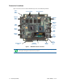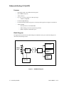
1
CMX32M cpuModules™ User’s Manual BDM-610000075 Revision D ® www.rtd.com ISO9001 and AS9100 Certified “Accessing the Analog World”® CMX32M cpuModules™ User’s Manual RTD Document Number: BDM-610000075 Revision D Copyright © 2009-2012 RTD Embedded Technologies, Inc. All rights reserved. Trademarks Advanced Analog I/O, Advanced Digital I/O, aAIO, aDIO, a2DIO, Autonomous SmartCal, “Catch the Express”, cpuModule, dspFramework, dspModule, expressMate, ExpressPlatform, HiDANplus, “MIL Value for COTS prices”, multiPort, PlatformBus, and PC/104EZ are trademarks, and “Accessing the Analog World”, dataModule, IDAN, HiDAN, RTD, and the RTD logo are registered trademarks of RTD Embedded Technologies, Inc (formerly Real Time Devices, Inc.). PS/2 is a trademark of International Business Ma¬chines Inc. PCI, PCI Express, and PCIe are trademarks of PCI-SIG. PC/104, PC/104-Plus, PCI-104, PCIe/104, PCI/104-Express and 104 are trademarks of the PC/104 Embedded Consortium. All other trademarks appearing in this doc¬ument are the property of their respective owners. Failure to follow the instructions found in this manual may result in damage to the product described in this manual, or other components of the system. The procedure set forth in this manual shall only be performed by persons qualified to service electronic equipment. Contents and specifications within this manual are given without warranty, and are subject to change without notice. RTD Embedded Technologies, Inc. shall not be liable for errors or omissions in this manual, or for any loss, damage, or injury in connection with the use of this manual. Revision History ii Revision Date A 6/13/11 Initial Release. B 7/11/11 Corrected Headphone Load Impedance in Table 4 on page 12. Corrected aAIO connector number in Table 26 on page 39. Corrected Audio pinout in Table 29 on page 42. C 2/17/12 Updated block diagram to clarify x1 links. Clarified the meaning of AD_RESULT register on page 73 Added CN numbers to Figure 11, IDAN-CMX32M Connectors,—page 100 D 9/21/12 Corrected LVDS Connector pin count and mating connector in Table 5, CMX32M Basic Connectors — 17 and Table 6, CMX32M Basic Connectors—25 CMX32M cpuModule Reason for Change BDM-610000075 Rev D CMX32M cpuModules™ ® www.rtd.com ISO9001 and AS9100 Certified “Accessing the Analog World”® iv CMX32M cpuModule BDM-610000075 Rev D Table of Contents Chapter 1 Introduction CMX32M cpuModules . . . . . . . . . . . . . . . . . . . . . . . . . . . . . . . . . . . . . . . . . . . . . . . . . . . . . . . . . . . . . . . . . . . . . . . . . . . . . . . . . 2 Enhanced Intel SpeedStep (Core 2 Duo only) . . . . . . . . . . . . . . . . . . . . . . . . . . . . . . . . . . . . . . . . . . . . . . . . . . . . . . . . . . . . . . . . . Thermal Monitor . . . . . . . . . . . . . . . . . . . . . . . . . . . . . . . . . . . . . . . . . . . . . . . . . . . . . . . . . . . . . . . . . . . . . . . . . . . . . . . . . . . . . . . . . . . . aDIO with Wake-on-aDIO. . . . . . . . . . . . . . . . . . . . . . . . . . . . . . . . . . . . . . . . . . . . . . . . . . . . . . . . . . . . . . . . . . . . . . . . . . . . . . . . . . . . 3 3 3 Ordering Information . . . . . . . . . . . . . . . . . . . . . . . . . . . . . . . . . . . . . . . . . . . . . . . . . . . . . . . . . . . . . . . . . . . . . . . . . . . . . . . . . 5 CMX32M Model Options . . . . . . . . . . . . . . . . . . . . . . . . . . . . . . . . . . . . . . . . . . . . . . . . . . . . . . . . . . . . . . . . . . . . . . . . . . . . . . . . . . . . Cable Kits and Accessories . . . . . . . . . . . . . . . . . . . . . . . . . . . . . . . . . . . . . . . . . . . . . . . . . . . . . . . . . . . . . . . . . . . . . . . . . . . . . . . . . . . 5 5 Board Features . . . . . . . . . . . . . . . . . . . . . . . . . . . . . . . . . . . . . . . . . . . . . . . . . . . . . . . . . . . . . . . . . . . . . . . . . . . . . . . . . . . . . . . . 6 I/O . . . . . . . . . . . . . . . . . . . . . . . . . . . . . . . . . . . . . . . . . . . . . . . . . . . . . . . . . . . . . . . . . . . . . . . . . . . . . . . . . . . . . . . . . . . . . . . . . . . . . . . . . . BIOS. . . . . . . . . . . . . . . . . . . . . . . . . . . . . . . . . . . . . . . . . . . . . . . . . . . . . . . . . . . . . . . . . . . . . . . . . . . . . . . . . . . . . . . . . . . . . . . . . . . . . . . . . Block Diagram . . . . . . . . . . . . . . . . . . . . . . . . . . . . . . . . . . . . . . . . . . . . . . . . . . . . . . . . . . . . . . . . . . . . . . . . . . . . . . . . . . . . . . . . . . . . . . . 7 9 10 Specifications. . . . . . . . . . . . . . . . . . . . . . . . . . . . . . . . . . . . . . . . . . . . . . . . . . . . . . . . . . . . . . . . . . . . . . . . . . . . . . . . . . . . . . . . . . 11 Physical Characteristics . . . . . . . . . . . . . . . . . . . . . . . . . . . . . . . . . . . . . . . . . . . . . . . . . . . . . . . . . . . . . . . . . . . . . . . . . . . . . . . . . . . . . . Power Consumption . . . . . . . . . . . . . . . . . . . . . . . . . . . . . . . . . . . . . . . . . . . . . . . . . . . . . . . . . . . . . . . . . . . . . . . . . . . . . . . . . . . . . . . . . Operating Conditions . . . . . . . . . . . . . . . . . . . . . . . . . . . . . . . . . . . . . . . . . . . . . . . . . . . . . . . . . . . . . . . . . . . . . . . . . . . . . . . . . . . . . . . . Electrical Characteristics . . . . . . . . . . . . . . . . . . . . . . . . . . . . . . . . . . . . . . . . . . . . . . . . . . . . . . . . . . . . . . . . . . . . . . . . . . . . . . . . . . . . . 11 11 11 12 Contact Information . . . . . . . . . . . . . . . . . . . . . . . . . . . . . . . . . . . . . . . . . . . . . . . . . . . . . . . . . . . . . . . . . . . . . . . . . . . . . . . . . . 14 Chapter 2 Getting Started Connector Locations . . . . . . . . . . . . . . . . . . . . . . . . . . . . . . . . . . . . . . . . . . . . . . . . . . . . . . . . . . . . . . . . . . . . . . . . . . . . . . . . . . 16 Selecting the Stack Order for the CMX32M . . . . . . . . . . . . . . . . . . . . . . . . . . . . . . . . . . . . . . . . . . . . . . . . . . . . . . . . . . . 18 Stack Example . . . . . . . . . . . . . . . . . . . . . . . . . . . . . . . . . . . . . . . . . . . . . . . . . . . . . . . . . . . . . . . . . . . . . . . . . . . . . . . . . . . . . . . . . 19 Connecting to the Stack . . . . . . . . . . . . . . . . . . . . . . . . . . . . . . . . . . . . . . . . . . . . . . . . . . . . . . . . . . . . . . . . . . . . . . . . . . . . . . . 20 Connecting the Utility Cable . . . . . . . . . . . . . . . . . . . . . . . . . . . . . . . . . . . . . . . . . . . . . . . . . . . . . . . . . . . . . . . . . . . . . . . . . . 21 Connecting a Keyboard. . . . . . . . . . . . . . . . . . . . . . . . . . . . . . . . . . . . . . . . . . . . . . . . . . . . . . . . . . . . . . . . . . . . . . . . . . . . . . . . 21 Booting the CMX32M cpuModule for the First Time . . . . . . . . . . . . . . . . . . . . . . . . . . . . . . . . . . . . . . . . . . . . . . . . . . 21 Chapter 3 Connecting the cpuModule Proper Grounding Techniques. . . . . . . . . . . . . . . . . . . . . . . . . . . . . . . . . . . . . . . . . . . . . . . . . . . . . . . . . . . . . . . . . . . . . . . . . 24 Connector Locations . . . . . . . . . . . . . . . . . . . . . . . . . . . . . . . . . . . . . . . . . . . . . . . . . . . . . . . . . . . . . . . . . . . . . . . . . . . . . . . . . . 24 Auxiliary Power (CN3). . . . . . . . . . . . . . . . . . . . . . . . . . . . . . . . . . . . . . . . . . . . . . . . . . . . . . . . . . . . . . . . . . . . . . . . . . . . . . . . . 26 Utility Port Connector (CN5). . . . . . . . . . . . . . . . . . . . . . . . . . . . . . . . . . . . . . . . . . . . . . . . . . . . . . . . . . . . . . . . . . . . . . . . . . 27 Speaker. . . . . . . . . . . . . . . . . . . . . . . . . . . . . . . . . . . . . . . . . . . . . . . . . . . . . . . . . . . . . . . . . . . . . . . . . . . . . . . . . . . . . . . . . . . . . . . . . . . . . . Keyboard . . . . . . . . . . . . . . . . . . . . . . . . . . . . . . . . . . . . . . . . . . . . . . . . . . . . . . . . . . . . . . . . . . . . . . . . . . . . . . . . . . . . . . . . . . . . . . . . . . . . Mouse. . . . . . . . . . . . . . . . . . . . . . . . . . . . . . . . . . . . . . . . . . . . . . . . . . . . . . . . . . . . . . . . . . . . . . . . . . . . . . . . . . . . . . . . . . . . . . . . . . . . . . . System Reset. . . . . . . . . . . . . . . . . . . . . . . . . . . . . . . . . . . . . . . . . . . . . . . . . . . . . . . . . . . . . . . . . . . . . . . . . . . . . . . . . . . . . . . . . . . . . . . . . Soft Power Button . . . . . . . . . . . . . . . . . . . . . . . . . . . . . . . . . . . . . . . . . . . . . . . . . . . . . . . . . . . . . . . . . . . . . . . . . . . . . . . . . . . . . . . . . . . Battery . . . . . . . . . . . . . . . . . . . . . . . . . . . . . . . . . . . . . . . . . . . . . . . . . . . . . . . . . . . . . . . . . . . . . . . . . . . . . . . . . . . . . . . . . . . . . . . . . . . . . . 27 28 28 28 28 29 SVGA Video Connector (CN18) . . . . . . . . . . . . . . . . . . . . . . . . . . . . . . . . . . . . . . . . . . . . . . . . . . . . . . . . . . . . . . . . . . . . . . . 30 BDM-610000075 Rev D Table of Contents v LVDS Flat Panel Video Connector (CN19) . . . . . . . . . . . . . . . . . . . . . . . . . . . . . . . . . . . . . . . . . . . . . . . . . . . . . . . . . . . . . 31 SATA Disk Chip Socket (U6) . . . . . . . . . . . . . . . . . . . . . . . . . . . . . . . . . . . . . . . . . . . . . . . . . . . . . . . . . . . . . . . . . . . . . . . . . . . 32 Installing and Configuring the SATA Disk Chip . . . . . . . . . . . . . . . . . . . . . . . . . . . . . . . . . . . . . . . . . . . . . . . . . . . . . . . . . . . . . . . . 32 Serial Port 1 (CN7) and Serial Port 2 (CN8) . . . . . . . . . . . . . . . . . . . . . . . . . . . . . . . . . . . . . . . . . . . . . . . . . . . . . . . . . . . 33 Serial Port UART . . . . . . . . . . . . . . . . . . . . . . . . . . . . . . . . . . . . . . . . . . . . . . . . . . . . . . . . . . . . . . . . . . . . . . . . . . . . . . . . . . . . . . . . . . . . . RS-232 Serial Port (Default) . . . . . . . . . . . . . . . . . . . . . . . . . . . . . . . . . . . . . . . . . . . . . . . . . . . . . . . . . . . . . . . . . . . . . . . . . . . . . . . . . . RS-422 or RS-485 Serial Port. . . . . . . . . . . . . . . . . . . . . . . . . . . . . . . . . . . . . . . . . . . . . . . . . . . . . . . . . . . . . . . . . . . . . . . . . . . . . . . . . . RS-422 and RS-485 Mode Pinout . . . . . . . . . . . . . . . . . . . . . . . . . . . . . . . . . . . . . . . . . . . . . . . . . . . . . . . . . . . . . . . . . . . . . . . . Dual Serial Port Modes. . . . . . . . . . . . . . . . . . . . . . . . . . . . . . . . . . . . . . . . . . . . . . . . . . . . . . . . . . . . . . . . . . . . . . . . . . . . . . . . . . . . . . . 33 33 34 35 36 Advanced Digital I/O (aDIO™) Port (CN6). . . . . . . . . . . . . . . . . . . . . . . . . . . . . . . . . . . . . . . . . . . . . . . . . . . . . . . . . . . . . 38 Advanced Analog I/O (aAIO™) Port (CN10) . . . . . . . . . . . . . . . . . . . . . . . . . . . . . . . . . . . . . . . . . . . . . . . . . . . . . . . . . . . 39 USB 2.0 Connector (CN17) . . . . . . . . . . . . . . . . . . . . . . . . . . . . . . . . . . . . . . . . . . . . . . . . . . . . . . . . . . . . . . . . . . . . . . . . . . . . 40 Ethernet (10/100/1000Base-T and -TX) Connectors (CN20 and CN30) . . . . . . . . . . . . . . . . . . . . . . . . . . . . . . . 41 High Definition Audio (CN11). . . . . . . . . . . . . . . . . . . . . . . . . . . . . . . . . . . . . . . . . . . . . . . . . . . . . . . . . . . . . . . . . . . . . . . . . 42 PCIe/104 Type 2 Bus (CN1 - Top) . . . . . . . . . . . . . . . . . . . . . . . . . . . . . . . . . . . . . . . . . . . . . . . . . . . . . . . . . . . . . . . . . . . . . . 43 PCIe/104 Type 2 Compatibility . . . . . . . . . . . . . . . . . . . . . . . . . . . . . . . . . . . . . . . . . . . . . . . . . . . . . . . . . . . . . . . . . . . . . . . . . . . . . . . PCIe Link Configuration . . . . . . . . . . . . . . . . . . . . . . . . . . . . . . . . . . . . . . . . . . . . . . . . . . . . . . . . . . . . . . . . . . . . . . . . . . . . . . . . . . . . . . PCIe Peer-To-Peer . . . . . . . . . . . . . . . . . . . . . . . . . . . . . . . . . . . . . . . . . . . . . . . . . . . . . . . . . . . . . . . . . . . . . . . . . . . . . . . . . . . . . . . . . . . . 45 46 46 PCIe/104 Type 1 Bus (CN2-Bottom) . . . . . . . . . . . . . . . . . . . . . . . . . . . . . . . . . . . . . . . . . . . . . . . . . . . . . . . . . . . . . . . . . . . 47 PCI/104-Express PCIe Bus Signals . . . . . . . . . . . . . . . . . . . . . . . . . . . . . . . . . . . . . . . . . . . . . . . . . . . . . . . . . . . . . . . . . . . . . . . . . . . . . PCI Express x16 Link . . . . . . . . . . . . . . . . . . . . . . . . . . . . . . . . . . . . . . . . . . . . . . . . . . . . . . . . . . . . . . . . . . . . . . . . . . . . . . . . . . . . . . . . . PCIe/104 Type 1 Compatibility . . . . . . . . . . . . . . . . . . . . . . . . . . . . . . . . . . . . . . . . . . . . . . . . . . . . . . . . . . . . . . . . . . . . . . . . . . . . . . . PCIe Link Configuration . . . . . . . . . . . . . . . . . . . . . . . . . . . . . . . . . . . . . . . . . . . . . . . . . . . . . . . . . . . . . . . . . . . . . . . . . . . . . . . . . . . . . . 49 49 50 50 Optional RTC Battery Input (CN13) . . . . . . . . . . . . . . . . . . . . . . . . . . . . . . . . . . . . . . . . . . . . . . . . . . . . . . . . . . . . . . . . . . . 51 Fan Power, Switched (CN15). . . . . . . . . . . . . . . . . . . . . . . . . . . . . . . . . . . . . . . . . . . . . . . . . . . . . . . . . . . . . . . . . . . . . . . . . . . 51 Chapter 4 Using the cpuModule The RTD Enhanced AMI BIOS . . . . . . . . . . . . . . . . . . . . . . . . . . . . . . . . . . . . . . . . . . . . . . . . . . . . . . . . . . . . . . . . . . . . . . . . . 54 Configuring the RTD Enhanced AMI BIOS . . . . . . . . . . . . . . . . . . . . . . . . . . . . . . . . . . . . . . . . . . . . . . . . . . . . . . . . . . . . . . . . . . . . Entering the BIOS Setup. . . . . . . . . . . . . . . . . . . . . . . . . . . . . . . . . . . . . . . . . . . . . . . . . . . . . . . . . . . . . . . . . . . . . . . . . . . . . . . . . . . . . . Field Selection . . . . . . . . . . . . . . . . . . . . . . . . . . . . . . . . . . . . . . . . . . . . . . . . . . . . . . . . . . . . . . . . . . . . . . . . . . . . . . . . . . . . . . . . . . . . . . . Main Menu Setup Fields . . . . . . . . . . . . . . . . . . . . . . . . . . . . . . . . . . . . . . . . . . . . . . . . . . . . . . . . . . . . . . . . . . . . . . . . . . . . . . . . . . . . . 54 54 54 55 Memory Map . . . . . . . . . . . . . . . . . . . . . . . . . . . . . . . . . . . . . . . . . . . . . . . . . . . . . . . . . . . . . . . . . . . . . . . . . . . . . . . . . . . . . . . . . . 56 I/O Address Map . . . . . . . . . . . . . . . . . . . . . . . . . . . . . . . . . . . . . . . . . . . . . . . . . . . . . . . . . . . . . . . . . . . . . . . . . . . . . . . . . . . . . . 57 Hardware Interrupts . . . . . . . . . . . . . . . . . . . . . . . . . . . . . . . . . . . . . . . . . . . . . . . . . . . . . . . . . . . . . . . . . . . . . . . . . . . . . . . . . . 58 Non-Standard Serial Port Modes . . . . . . . . . . . . . . . . . . . . . . . . . . . . . . . . . . . . . . . . . . . . . . . . . . . . . . . . . . . . . . . . . . . . . . 59 Advanced Digital I/O Ports (aDIO™). . . . . . . . . . . . . . . . . . . . . . . . . . . . . . . . . . . . . . . . . . . . . . . . . . . . . . . . . . . . . . . . . . . 60 Digital I/O Register Set . . . . . . . . . . . . . . . . . . . . . . . . . . . . . . . . . . . . . . . . . . . . . . . . . . . . . . . . . . . . . . . . . . . . . . . . . . . . . . . . . . . . . . . Port 1 Data register is a read/write byte direction . . . . . . . . . . . . . . . . . . . . . . . . . . . . . . . . . . . . . . . . . . . . . . . . . . . . . . . . Interrupts . . . . . . . . . . . . . . . . . . . . . . . . . . . . . . . . . . . . . . . . . . . . . . . . . . . . . . . . . . . . . . . . . . . . . . . . . . . . . . . . . . . . . . . . . . . . . . . . . . . Advanced Digital Interrupts . . . . . . . . . . . . . . . . . . . . . . . . . . . . . . . . . . . . . . . . . . . . . . . . . . . . . . . . . . . . . . . . . . . . . . . . . . . . . Event Mode . . . . . . . . . . . . . . . . . . . . . . . . . . . . . . . . . . . . . . . . . . . . . . . . . . . . . . . . . . . . . . . . . . . . . . . . . . . . . . . . . . . . . . . . . . . . . Match Mode . . . . . . . . . . . . . . . . . . . . . . . . . . . . . . . . . . . . . . . . . . . . . . . . . . . . . . . . . . . . . . . . . . . . . . . . . . . . . . . . . . . . . . . . . . . . Strobe Mode . . . . . . . . . . . . . . . . . . . . . . . . . . . . . . . . . . . . . . . . . . . . . . . . . . . . . . . . . . . . . . . . . . . . . . . . . . . . . . . . . . . . . . . . . . . . 60 62 62 62 62 62 63 vi CMX32M cpuModule BDM-610000075 Rev D Wake-on-aDIO . . . . . . . . . . . . . . . . . . . . . . . . . . . . . . . . . . . . . . . . . . . . . . . . . . . . . . . . . . . . . . . . . . . . . . . . . . . . . . . . . . . . . . . . . . . . . . 63 Advanced Analog I/O (aAIO) . . . . . . . . . . . . . . . . . . . . . . . . . . . . . . . . . . . . . . . . . . . . . . . . . . . . . . . . . . . . . . . . . . . . . . . . . . 64 Features . . . . . . . . . . . . . . . . . . . . . . . . . . . . . . . . . . . . . . . . . . . . . . . . . . . . . . . . . . . . . . . . . . . . . . . . . . . . . . . . . . . . . . . . . . . . . . . . . . . . . Block Diagram . . . . . . . . . . . . . . . . . . . . . . . . . . . . . . . . . . . . . . . . . . . . . . . . . . . . . . . . . . . . . . . . . . . . . . . . . . . . . . . . . . . . . . . . . . . . . . . Analog Inputs . . . . . . . . . . . . . . . . . . . . . . . . . . . . . . . . . . . . . . . . . . . . . . . . . . . . . . . . . . . . . . . . . . . . . . . . . . . . . . . . . . . . . . . . . . . . . . . Channel-Gain Table . . . . . . . . . . . . . . . . . . . . . . . . . . . . . . . . . . . . . . . . . . . . . . . . . . . . . . . . . . . . . . . . . . . . . . . . . . . . . . . . . . . . . . . . . . Analog to Digital Converter . . . . . . . . . . . . . . . . . . . . . . . . . . . . . . . . . . . . . . . . . . . . . . . . . . . . . . . . . . . . . . . . . . . . . . . . . . . . . . . . . . Programmable Digital Filter . . . . . . . . . . . . . . . . . . . . . . . . . . . . . . . . . . . . . . . . . . . . . . . . . . . . . . . . . . . . . . . . . . . . . . . . . . . . . . . . . . Threshold Detect . . . . . . . . . . . . . . . . . . . . . . . . . . . . . . . . . . . . . . . . . . . . . . . . . . . . . . . . . . . . . . . . . . . . . . . . . . . . . . . . . . . . . . . . . . . . Data Output. . . . . . . . . . . . . . . . . . . . . . . . . . . . . . . . . . . . . . . . . . . . . . . . . . . . . . . . . . . . . . . . . . . . . . . . . . . . . . . . . . . . . . . . . . . . . . . . . Direct Read . . . . . . . . . . . . . . . . . . . . . . . . . . . . . . . . . . . . . . . . . . . . . . . . . . . . . . . . . . . . . . . . . . . . . . . . . . . . . . . . . . . . . . . . . . . . . DMA Engine . . . . . . . . . . . . . . . . . . . . . . . . . . . . . . . . . . . . . . . . . . . . . . . . . . . . . . . . . . . . . . . . . . . . . . . . . . . . . . . . . . . . . . . . . . . . Operating Modes . . . . . . . . . . . . . . . . . . . . . . . . . . . . . . . . . . . . . . . . . . . . . . . . . . . . . . . . . . . . . . . . . . . . . . . . . . . . . . . . . . . . . . . . . . . . Simple Operation . . . . . . . . . . . . . . . . . . . . . . . . . . . . . . . . . . . . . . . . . . . . . . . . . . . . . . . . . . . . . . . . . . . . . . . . . . . . . . . . . . . . . . . DMA Based Operation . . . . . . . . . . . . . . . . . . . . . . . . . . . . . . . . . . . . . . . . . . . . . . . . . . . . . . . . . . . . . . . . . . . . . . . . . . . . . . . . . . Registers . . . . . . . . . . . . . . . . . . . . . . . . . . . . . . . . . . . . . . . . . . . . . . . . . . . . . . . . . . . . . . . . . . . . . . . . . . . . . . . . . . . . . . . . . . . . . . . . . . . . . Register Map . . . . . . . . . . . . . . . . . . . . . . . . . . . . . . . . . . . . . . . . . . . . . . . . . . . . . . . . . . . . . . . . . . . . . . . . . . . . . . . . . . . . . . . . . . . . Control Registers . . . . . . . . . . . . . . . . . . . . . . . . . . . . . . . . . . . . . . . . . . . . . . . . . . . . . . . . . . . . . . . . . . . . . . . . . . . . . . . . . . . . . . . . Channel Gain Table Registers . . . . . . . . . . . . . . . . . . . . . . . . . . . . . . . . . . . . . . . . . . . . . . . . . . . . . . . . . . . . . . . . . . . . . . . . . . . . BIOS Setup Register . . . . . . . . . . . . . . . . . . . . . . . . . . . . . . . . . . . . . . . . . . . . . . . . . . . . . . . . . . . . . . . . . . . . . . . . . . . . . . . . . . . . . Usage Notes . . . . . . . . . . . . . . . . . . . . . . . . . . . . . . . . . . . . . . . . . . . . . . . . . . . . . . . . . . . . . . . . . . . . . . . . . . . . . . . . . . . . . . . . . . . . . . . . . Board Open. . . . . . . . . . . . . . . . . . . . . . . . . . . . . . . . . . . . . . . . . . . . . . . . . . . . . . . . . . . . . . . . . . . . . . . . . . . . . . . . . . . . . . . . . . . . . Changing Ranges . . . . . . . . . . . . . . . . . . . . . . . . . . . . . . . . . . . . . . . . . . . . . . . . . . . . . . . . . . . . . . . . . . . . . . . . . . . . . . . . . . . . . . . . 64 64 65 65 65 65 66 67 67 67 67 67 67 68 68 69 71 77 77 77 77 Real Time Clock Control. . . . . . . . . . . . . . . . . . . . . . . . . . . . . . . . . . . . . . . . . . . . . . . . . . . . . . . . . . . . . . . . . . . . . . . . . . . . . . . 78 Overview . . . . . . . . . . . . . . . . . . . . . . . . . . . . . . . . . . . . . . . . . . . . . . . . . . . . . . . . . . . . . . . . . . . . . . . . . . . . . . . . . . . . . . . . . . . . . . . . . . . . Accessing the RTC Registers . . . . . . . . . . . . . . . . . . . . . . . . . . . . . . . . . . . . . . . . . . . . . . . . . . . . . . . . . . . . . . . . . . . . . . . . . . . . . . . . . . 78 78 Watchdog Timer Control . . . . . . . . . . . . . . . . . . . . . . . . . . . . . . . . . . . . . . . . . . . . . . . . . . . . . . . . . . . . . . . . . . . . . . . . . . . . . . 80 Thermal Management . . . . . . . . . . . . . . . . . . . . . . . . . . . . . . . . . . . . . . . . . . . . . . . . . . . . . . . . . . . . . . . . . . . . . . . . . . . . . . . . . 81 Thermal Monitor . . . . . . . . . . . . . . . . . . . . . . . . . . . . . . . . . . . . . . . . . . . . . . . . . . . . . . . . . . . . . . . . . . . . . . . . . . . . . . . . . . . . . . . . . . . . Fan Mode . . . . . . . . . . . . . . . . . . . . . . . . . . . . . . . . . . . . . . . . . . . . . . . . . . . . . . . . . . . . . . . . . . . . . . . . . . . . . . . . . . . . . . . . . . . . . . . . . . . Further Temperature Reduction . . . . . . . . . . . . . . . . . . . . . . . . . . . . . . . . . . . . . . . . . . . . . . . . . . . . . . . . . . . . . . . . . . . . . . . . . . . . . . 81 81 81 Power Management . . . . . . . . . . . . . . . . . . . . . . . . . . . . . . . . . . . . . . . . . . . . . . . . . . . . . . . . . . . . . . . . . . . . . . . . . . . . . . . . . . . 82 Enabling Enhanced Intel SpeedStep Technology (Core 2 Duo) . . . . . . . . . . . . . . . . . . . . . . . . . . . . . . . . . . . . . . . . . . . . . . . . . Advanced Configuration and Power Interface (ACPI) . . . . . . . . . . . . . . . . . . . . . . . . . . . . . . . . . . . . . . . . . . . . . . . . . . . . . . . . . Power Button Modes . . . . . . . . . . . . . . . . . . . . . . . . . . . . . . . . . . . . . . . . . . . . . . . . . . . . . . . . . . . . . . . . . . . . . . . . . . . . . . . . . . . . . . . . Low-Power Wake Options. . . . . . . . . . . . . . . . . . . . . . . . . . . . . . . . . . . . . . . . . . . . . . . . . . . . . . . . . . . . . . . . . . . . . . . . . . . . . . . . . . . . AT vs. ATX Power Supplies . . . . . . . . . . . . . . . . . . . . . . . . . . . . . . . . . . . . . . . . . . . . . . . . . . . . . . . . . . . . . . . . . . . . . . . . . . . . . . . . . . . ATX Power Supply Signals . . . . . . . . . . . . . . . . . . . . . . . . . . . . . . . . . . . . . . . . . . . . . . . . . . . . . . . . . . . . . . . . . . . . . . . . . . . . . . . . . . . . Reducing Power Consumption . . . . . . . . . . . . . . . . . . . . . . . . . . . . . . . . . . . . . . . . . . . . . . . . . . . . . . . . . . . . . . . . . . . . . . . . . . . . . . . 82 82 82 82 83 83 83 Multi-Color LED . . . . . . . . . . . . . . . . . . . . . . . . . . . . . . . . . . . . . . . . . . . . . . . . . . . . . . . . . . . . . . . . . . . . . . . . . . . . . . . . . . . . . . . 84 Reset Status Register . . . . . . . . . . . . . . . . . . . . . . . . . . . . . . . . . . . . . . . . . . . . . . . . . . . . . . . . . . . . . . . . . . . . . . . . . . . . . . . . . . 85 Features and Settings That Can Affect Boot Time . . . . . . . . . . . . . . . . . . . . . . . . . . . . . . . . . . . . . . . . . . . . . . . . . . . . . 87 Quick Boot . . . . . . . . . . . . . . . . . . . . . . . . . . . . . . . . . . . . . . . . . . . . . . . . . . . . . . . . . . . . . . . . . . . . . . . . . . . . . . . . . . . . . . . . . . . . . . . . . . Add-On Cards With BIOS Extensions . . . . . . . . . . . . . . . . . . . . . . . . . . . . . . . . . . . . . . . . . . . . . . . . . . . . . . . . . . . . . . . . . . . . . . . . . VGA Controller . . . . . . . . . . . . . . . . . . . . . . . . . . . . . . . . . . . . . . . . . . . . . . . . . . . . . . . . . . . . . . . . . . . . . . . . . . . . . . . . . . . . . . . . . . . . . . Hard Drive Type . . . . . . . . . . . . . . . . . . . . . . . . . . . . . . . . . . . . . . . . . . . . . . . . . . . . . . . . . . . . . . . . . . . . . . . . . . . . . . . . . . . . . . . . . . . . . Monitor Type . . . . . . . . . . . . . . . . . . . . . . . . . . . . . . . . . . . . . . . . . . . . . . . . . . . . . . . . . . . . . . . . . . . . . . . . . . . . . . . . . . . . . . . . . . . . . . . . NVRAM Updates . . . . . . . . . . . . . . . . . . . . . . . . . . . . . . . . . . . . . . . . . . . . . . . . . . . . . . . . . . . . . . . . . . . . . . . . . . . . . . . . . . . . . . . . . . . . 87 87 87 87 87 87 BDM-610000075 Rev D Table of Contents vii Boot Device Order . . . . . . . . . . . . . . . . . . . . . . . . . . . . . . . . . . . . . . . . . . . . . . . . . . . . . . . . . . . . . . . . . . . . . . . . . . . . . . . . . . . . . . . . . . . 87 System Recovery. . . . . . . . . . . . . . . . . . . . . . . . . . . . . . . . . . . . . . . . . . . . . . . . . . . . . . . . . . . . . . . . . . . . . . . . . . . . . . . . . . . . . . . 88 Reset Button Recovery . . . . . . . . . . . . . . . . . . . . . . . . . . . . . . . . . . . . . . . . . . . . . . . . . . . . . . . . . . . . . . . . . . . . . . . . . . . . . . . . . . . . . . . Load Default BIOS Settings. . . . . . . . . . . . . . . . . . . . . . . . . . . . . . . . . . . . . . . . . . . . . . . . . . . . . . . . . . . . . . . . . . . . . . . . . . . . . . . . . . . Serial Power On Self Test POST Code Output . . . . . . . . . . . . . . . . . . . . . . . . . . . . . . . . . . . . . . . . . . . . . . . . . . . . . . . . . . . . . . . . . BIOS Boot Block Recovery. . . . . . . . . . . . . . . . . . . . . . . . . . . . . . . . . . . . . . . . . . . . . . . . . . . . . . . . . . . . . . . . . . . . . . . . . . . . . . . . . . . . 88 88 88 88 Appendix A Hardware Reference Jumper Settings and Locations . . . . . . . . . . . . . . . . . . . . . . . . . . . . . . . . . . . . . . . . . . . . . . . . . . . . . . . . . . . . . . . . . . . . . . . . 90 Onboard PCI/PCIe Devices . . . . . . . . . . . . . . . . . . . . . . . . . . . . . . . . . . . . . . . . . . . . . . . . . . . . . . . . . . . . . . . . . . . . . . . . . . . . 92 Physical Dimensions . . . . . . . . . . . . . . . . . . . . . . . . . . . . . . . . . . . . . . . . . . . . . . . . . . . . . . . . . . . . . . . . . . . . . . . . . . . . . . . . . . . 93 Board Spacing . . . . . . . . . . . . . . . . . . . . . . . . . . . . . . . . . . . . . . . . . . . . . . . . . . . . . . . . . . . . . . . . . . . . . . . . . . . . . . . . . . . . . . . . . . . . . . . 93 Appendix B Troubleshooting Common Problems and Solutions . . . . . . . . . . . . . . . . . . . . . . . . . . . . . . . . . . . . . . . . . . . . . . . . . . . . . . . . . . . . . . . . . . . . . 96 Troubleshooting a PC/104 System. . . . . . . . . . . . . . . . . . . . . . . . . . . . . . . . . . . . . . . . . . . . . . . . . . . . . . . . . . . . . . . . . . . . . 97 How to Obtain Technical Support . . . . . . . . . . . . . . . . . . . . . . . . . . . . . . . . . . . . . . . . . . . . . . . . . . . . . . . . . . . . . . . . . . . . . 98 Appendix C IDAN™ Dimensions and Pinout IDAN Dimensions and Connectors . . . . . . . . . . . . . . . . . . . . . . . . . . . . . . . . . . . . . . . . . . . . . . . . . . . . . . . . . . . . . . . . . . . . 100 External I/O Connections . . . . . . . . . . . . . . . . . . . . . . . . . . . . . . . . . . . . . . . . . . . . . . . . . . . . . . . . . . . . . . . . . . . . . . . . . . . . . 101 Appendix D Additional Information Application Notes . . . . . . . . . . . . . . . . . . . . . . . . . . . . . . . . . . . . . . . . . . . . . . . . . . . . . . . . . . . . . . . . . . . . . . . . . . . . . . . . . . . . . 109 Drivers and Example Programs . . . . . . . . . . . . . . . . . . . . . . . . . . . . . . . . . . . . . . . . . . . . . . . . . . . . . . . . . . . . . . . . . . . . . . . . 109 Interrupt Programming . . . . . . . . . . . . . . . . . . . . . . . . . . . . . . . . . . . . . . . . . . . . . . . . . . . . . . . . . . . . . . . . . . . . . . . . . . . . . . . 109 Serial Port Programming . . . . . . . . . . . . . . . . . . . . . . . . . . . . . . . . . . . . . . . . . . . . . . . . . . . . . . . . . . . . . . . . . . . . . . . . . . . . . . 109 PC/104Specifications. . . . . . . . . . . . . . . . . . . . . . . . . . . . . . . . . . . . . . . . . . . . . . . . . . . . . . . . . . . . . . . . . . . . . . . . . . . . . . . . . . 109 Appendix E viii Limited Warranty CMX32M cpuModule BDM-610000075 Rev D Chapter 1 Introduction This manual provides comprehensive hardware and software information for users developing with the CMX32M PCIe/104 cpuModule. Note Read the specifications beginning on page 11 prior to designing with the cpuModule. This manual is organized as follows: Chapter 1 Introduction introduces main features and specifications Chapter 2 Getting Started provides abbreviated instructions to get started quickly Chapter 3 Connecting the cpuModule provides information on connecting the cpuModule to peripherals Chapter 4 Using the cpuModule provides information to develop applications for the cpuModule, including general cpuModule information, detailed information on storing both applications and system functions, and using utility programs Appendix A Hardware Reference lists jumper locations and settings, physical dimensions, and processor thermal management Appendix B Troubleshooting offers advice on debugging problems with your system Appendix C IDAN™ Dimensions and Pinout provides connector pinouts for the cpuModule installed in an RTD Intelligent Data Acquisition Node (IDAN) frame Appendix D Additional Information lists sources and websites to support the cpuModule installation and configuration Appendix E Limited Warranty BDM-610000075 Rev D Chapter 1: Introduction 1 CMX32M cpuModules RTD's CMX32M cpuModule represents the latest in high-performance, energy-efficient embedded computing solutions. Based on the Intel® “Montevina” platform, it features a 64-bit “Penryn” processor coupled with a GS45 chipset. It includes a source-synchronous Front-Side-Bus (FSB) operating up to 1066 MHz, and up to 6 MB of L2 cache. This cpuModule is available either with a dual-core Core 2 Duo processor, or a single core Celeron-M processor. The Core 2 Duo processor features Enhanced Intel SpeedStep® technology, which enables real-time dynamic switching between multiple voltage and frequency points. This results in optimal performance without compromising low power. A dual channel DDR2 memory interface operating at up to 800 MHz ensures adequate memory bandwidth to keep up with both processors. All memory chips are soldered directly onto the board. The video interface is provided by an Analog SVGA output and an LVDS flat panel output. The two outputs are independent, and can display separate images and display timings. Maximum resolution is 2048 x 1536. High-speed peripheral connections include USB 2.0, with up to 480 Mb/sec data throughput. A Serial-ATA (SATA) controller provides a fast 3.0 Gbps connection to the hard drives. Network connectivity is provided by an integrated 10/100/1000 Mbps Ethernet controller. Other features include two RS-232/422/485 COM ports, AC97 audio, Advanced Analog I/O (aAIO), and Advanced Digital I/O (aDIO). RTD has gone the extra mile to include additional advanced features for maximum flexibility. These include a SATA Disk Chip socket that allows flash drive with a standard SATA interface to be attached to the board, either socketed or soldered. An Advanced Watchdog Timer is provided that can generate an interrupt or reset when the timer expires. SDRAM is soldered directly to the board for high vibration resistance. The CMX32M is also available in a rugged, fanless IDAN enclosure. SVGA Video (CN18) Ethernet(CN30) HD Audio(CN11) LVDS Flat Panel (CN19) COM2&4 (CN8) COM1&3 (CN7) aAIO (CN10) Switched Fan (CN15) USB 2.0 (CN17) aDIO (CN6) Ethernet (CN20) MultiFunction (CN5) PCIe Bus (CN1 & CN2) Auxiliary Power (CN3) Figure 1 2 CMX32M cpuModule Battery (CN13) SATA Disk Chip (U6) CMX32M cpuModule (top view) BDM-610000075 Rev D Enhanced Intel SpeedStep (Core 2 Duo only) Enhanced Intel® SpeedStep® Technology has revolutionized thermal and power management by giving operating systems greater control over the processor’s operating frequency and input voltage. Systems can easily manage power consumption dynamically. Today’s embedded systems are demanding greater performance at equivalent levels of power consumption. Legacy hardware support for backplanes, board sizes and thermal solutions have forced design teams to place greater emphasis on power and thermal budgets. Intel has extended architectural innovation for saving power by implementing new features such as Enhanced Intel SpeedStep Technology. Enhanced Intel SpeedStep Technology allows the processor performance and power consumption levels to be modified while a system is functioning. This is accomplished via operating system or application software, which changes the processor speed and the processor core voltage while the system is operating. A variety of inputs such as system power source, processor thermal state, or operating system policy are used to determine the proper operating state. The software model behind Enhanced Intel SpeedStep Technology has ultimate control over the frequency and voltage transitions. This software model is a major step forward over previous implementations of Intel SpeedStep technology. Legacy versions of Intel SpeedStep technology required hardware support through the chipset. Enhanced Intel SpeedStep Technology has removed the chipset hardware requirement and only requires the support of the voltage regulator, processor and operating system. Centralization of the control mechanism and software interface to the processor, and reduced hardware overhead has reduced processor core unavailability time to 10 μs from the previous generation unavailability of 250 μs. Thermal Monitor The Intel ® Thermal Monitor is a feature on the CMX32M that automatically throttles the CPU when the CPU exceeds its thermal limit. This allows the processor to operate for short durations at a higher frequency than the thermal solution or ambient temperature would otherwise allow. The thermal limit and duty cycle of the Thermal Monitor cannot be modified. A second thermal monitor is used to throttle the memory interface when the memory controller or the memory approaches it’s thermal limit. This ensures proper operation even under the harshest conditions. The thermal monitors operate independently of each other. aDIO with Wake-on-aDIO RTD’s exclusive aDIO™ is 12 digital bits configured as 8 bit-direction programmable and 4-bit port-direction programmable I/O, plus 2 strobe inputs giving you any combination of inputs and outputs. Match, event, and strobe interrupt modes mean no more wasting valuable processor time polling digital inputs. Interrupts are generated when the 8 bit-direction programmable digital inputs match a pattern or on any value change event. Bit masking allows selecting any subgroup of eight bits. The strobe input latches data into the bit-programmable port and generates an interrupt. Any of the interrupt modes can be used to generate a wake event from any standby/powerdown mode. aAIO RTD’s exclusive aAIO™ provides 8 single-ended or 4 differential analog inputs, providing a single-board, data acquisition solution. Each input can have a range or +/-5V, +/- 10V, 0-5V, or 0-10V. A maximum sample rate of 100kHz is shared between the channels. A minimum sample rate of 9mHz (one sample every 107 seconds) allows unobtrusive background monitoring of signals. The input range and mode (differential vs. single ended) can be individually selected for each channel. Any number of channels can be selected for sampling. Advanced features include a programmable, single-pole IIR filter on each channel. This allows the hardware to remove noise from the input signal. The filter can be individually enabled and the coefficients adjusted for each channel. The cutoff frequency can be adjusted down to 0.12% of the sample rate. BDM-610000075 Rev D Chapter 1: Introduction 3 The aAIO also provides interrupts on threshold crossing. A high and low threshold can be set for each channel. After sampling is started, an interrupt can be generated if any of the signals cross the threshold. This removes some of the CPU load for simple monitoring tasks. A DMA engine with a scatter-gather table allows efficient, robust handling of data. Up to 64 DMA buffers can be assigned to each channel. After filling each buffer, an interrupt can be generated to inform the driver that buffer is full so that the driver can empty it or assign a new buffer. Because many buffers can be assigned, interrupt latency problems are mitigated. Also, since each channel has it’s own buffer, software does not have to de-interlace the data. The DMA engine can send the data to anywhere in 4GB memory space. 4 CMX32M cpuModule BDM-610000075 Rev D Ordering Information The CMX32M cpuModule is available with a selection of processors and memory sizes. The cpuModule can also be purchased as part of an Intelligent Data Acquisition Node (IDAN™) building block, which consists of the cpuModule and a milled aluminum IDAN frame. The IDAN building block can be used in just about any combination with other IDAN building blocks to create a simple but rugged PC/104 stack. Refer to Appendix C, IDAN™ Dimensions and Pinout, for more information. The CMX32M cpuModule can also be purchased as part of a custom-built RTD HiDAN™ or HiDANplus High Reliability Intelligent Data Acquisition Node. Contact RTD for more information on its high reliability PC-104 systems. CMX32M Model Options The basic cpuModule model options are shown below. Refer to the RTD website (www.rtd.com) for more detailed ordering information and any new variations that may be available. Table 1 CMX32M cpuModule Model Options Part Number Description CMX32MVD1860HR-2048 Core 2 Duo (Dual Core) 1.86 GHz, 2GB DDR2-SDRAM CMX32MVD1860HR-1024 Core 2 Duo (Dual Core) 1.86 GHz, 1GB DDR2-SDRAM CMX32MVD1200HR-2048 Core 2 Duo (Dual Core) 1.20 GHz, 2GB DDR2-SDRAM CMX32MVD1200HR-1024 Core 2 Duo (Dual Core) 1.20 GHz, 1GB DDR2-SDRAM CMX32MCS1200HR-2048 Celeron (Single Core) 1.20 GHz, 2GB DDR2-SDRAM CMX32MCS1200HR-1024 Celeron (Single Core) 1.20 GHz, 1GB DDR2-SDRAM Cable Kits and Accessories For maximum flexibility, RTD does not provide cables with the cpuModule. You may wish to purchase the CMX32M cpuModule cable kit (P/N XK-CM95), which contains: • • • • • • • • Multi-function utility harness (keyboard socket, battery, reset, speaker) Two serial port cables (DIL-10 to DSUB-9) VGA monitor cable (DIL-10 to high density 15-pin DSUB) aDIO cable (DIL-16 to DSUB-25) Two USB cables (5-pin SIL to USB A) PCIe/104 Type 2 break-out board (to connect SATA and USB) Audio Cable (DIL-16 to five 3.5mm Jacks) Two Ethernet cables (DIL-10 to RJ-45) For additional accessories, refer to the RTD website. BDM-610000075 Rev D Chapter 1: Introduction 5 Board Features • • • • • • • 6 Penryn Processor Part Number Speed Cores L2 Cache FSB Speed CMX32MVD1860 1.86GHZ Two 6 MB 1066 MHz CMX32MVD1200 1.20 GHz Two 3 MB 800 MHz CMX32MCS1200 1.20 GHz One 1 MB 800 MHz – Intel 64 architecture for 64-bit processing. – Enhanced Intel SpeedStep Technology and dynamic FSB frequency switching (Core 2 Duo only). – Enhanced Intel Dynamic Acceleration Technology and Enhanced Multi-Threaded Thermal Management (Core 2 Duo only) – Supports enhanced Intel Virtualization Technology (Core 2 Duo only) – 45 nm process 1 GB or 2GBytes BGA DDR2 SDRAM – Dual-channel memory interface – Up to 800MHz Data Rate per channel – Surface Mounted for maximum reliability Stackable 156-pin PCIe/104 Type 2 bus on top – Four PCI Express x1 Lanes – Two SATA 2.0 – Two USB 2.0 – SMBus Stackable 156-pin PCIe/104 Type 1 bus on bottom – Four PCI Express x1 Lanes – One PCI Express x16 Lane – Two USB 2.0 – SMBus Advanced Thermal Management – Thermal Monitor throttles processor and memory to prevent thermal runaway – Auto Fan Control only runs fan when needed – SMBus Temperature Monitor for CPU and board temperature – Mini Fan Heatsink with Auto Fan control – Passive Structural Heatsink & Heatpipes in IDAN and HiDAN System Configurations Advanced Programmable Interrupt Controller (APIC) – 24 interrupt channels with APIC enabled (15 in legacy PIC mode) – High Precision Event Timer Advanced Configuration and Power Interface (ACPI) – ACPI 3.0 Compliant – Supported power down modes: S1 (Power On Suspend), S3 (Suspend to RAM), S4 (Hibernate), and S5 (Soft-Off) – CPU Clock Throttling and Clock Stop for C0 to C6 Support CMX32M cpuModule BDM-610000075 Rev D – Wake events include: • • • • • • • • • • • aDIO Interrupt Wake-on-LAN Real Time Clock COM port Ring Power Switch etc. Network Boot supported by Intel PXE Y2K compliant Real-Time Clock (external battery required) Nonvolatile storage of CMOS settings without battery Advanced Watchdog timer Complete PC-compatible Single Board Computer I/O • • • • BDM-610000075 SVGA controller Onboard with 3D Acceleration – Intel Graphics Media Accelerator 4500MHD – Generation 5.0 graphics engine with 10 cores – Dynamic Video Memory (up to 256MB) – DirectX 10 Support – Supports Windows Vista Aero “Glass” Effects – Analog SVGA Output – LVDS Flat Panel output Two Gigabit Ethernet – Intel 82567LM PHY + ICH9M Controller (PRO1000 Series) – Intel 82574IT Controller (PRO1000 Series) – 10/100/1000 Auto-negotiation – Jumbo Frame Support (9kB) – PXE network Boot – Smart Speed operation for automatic speed reduction on faulty cable plants – Automatic MDI/MDI-X crossover capable Software-configurable RS-232/422/485 serial ports – 16550 compatible UARTs for high-speed – 120 Ohm Termination resistors for RS-422/485 through BIOS Configuration – Each serial port connector can be configured as two limited serial ports, for a total of four serial ports – Fully jumperless configuration Advanced Digital I/O (aDIO) – One 8-bit bit-programmable I/O with Advanced Digital Interrupt Modes – One 4-bit port programmable as input or output – Event Mode Interrupt generates an interrupt when any input bit changes – Match Mode Interrupt generates an interrupt when input bits match a preset value Rev D Chapter 1: Introduction 7 • – External Strobe Mode latches 8 data inputs and generates and interrupt – Two Strobes can be configured as readable inputs Advanced Analog I/O (aAIO) – Eight single-ended or four differential analog inputs – Up to 100kHz sample rate – 16-bit resolution – 0 to +5V, +/-5V, 0 to +10V, and +/-10V input ranges – Per-channel digital filtering – Per-channel threshold detection generates an interrupt when signal crosses high or low threshold. – Advanced DMA • • • • • • • • • 8 Buffer chaining prevents interrupt latency problems DMA to anywhere in 4GB address space Two USB 2.0 (Universal Serial Bus) Ports – Supports 480 Mb/s (high-speed), 12Mb/s (full-speed), and 1.5Mbs (low speed) peripherals – 500 mA @ 5 Vdc provided per port – USB Boot capability Serial ATA (SATA) with RAID support – Transfer rate up to 3Gb/sec – Integrated AHCI controller – RAID 0 and 1 supported through Intel Matrix Storage Technology – Compatability mode supports legacy operating systems. SATA Disk Chip Socket – Miniature SATA Flash Disk Chip – Capacities up to 32GB1 – Natively supported by all major operating systems High Definition Audio Support – 5.1 Surround Line Output – Headphone Output – Line level input – Microphone input Utility port – PC/AT compatible keyboard port – PS/2 Mouse Port – Speaker port (0.1W output) – Hardware Reset input – Soft Power Button input – Battery input for Real Time Clock Power I/O – 1. Each channel has its own DMA buffer ATX Power signals During the time of this manual’s publication, 32GB was the largest available SATA Disk Chip capacity CMX32M cpuModule BDM-610000075 Rev D BIOS • • • • RTD Enhanced AMI BIOS User-configurable using built-in Setup program Nonvolatile storage of CMOS settings without battery Boot Devices – Standard Devices (floppy disk, hard disk, etc.) – SATA Disk Chip – USB Device – Network – Fail Safe Boot ROM • • BDM-610000075 Surface-mount Flash chip that holds ROM-DOS™ Quick Boot mode Rev D Chapter 1: Introduction 9 Block Diagram The next figure shows a simplified block diagram of the CMX32M cpuModule. Figure 2 CMX32M cpuModule Simplified Block Diagram You can easily customize the cpuModule by stacking PCI/104-Express or PCIe/104 modules such as video controllers, Digital Signal Processors, drive carriers, LAN controllers, or analog and digital data acquisition modules. Stacking modules onto the cpuModule avoids expensive installations of backplanes and card cages, and preserves the module's compactness. The cpuModule uses the RTD Enhanced AMI BIOS. Drivers in the BIOS allow booting from hard disk, Disk Chip, or boot block flash, thus enabling the system to be used with traditional disk drives or nonmechanical drives. Boot from USB devices and network are also supported. The cpuModule and BIOS are also compatible with any real-time operating systems for PC compatible computers, although these may require creation of custom drivers to use the aDIO, aAIO, and watchdog timer. 10 CMX32M cpuModule BDM-610000075 Rev D Specifications Physical Characteristics • • Dimensions: 116mm L x 99mm W x 24mm H (4.6"L x 3.9"W x 0.95"H) Weight: Approximately 0.20 Kg (0.44 lb.) with Heatsink Power Consumption Exact power consumption depends on the actual application. Table 2 lists power consumption for typical configurations and clock speeds. Table 2 Module cpuModule Power Consumption Speed RAM Power, Typ. Heavy CPU Load Heavy CPU & Gfx Load CMX32MVD1860 1.86 GHz 1024 MB 21.0 W 31.5 W 33.0 W CMX32MVD1200 1.20 GHz 1024 MB 15.8 W 21.0 W 23.0 W CMX32MCS1200 1.20 GHz 1024 MB 13.3 W 16.0 W 19.5 W Operating Conditions Table 3 Symbol Parameter VCC5 5V Supply Voltage VCC3 VCC12 VCCSTBY Operating Conditions Test Condition 3.3V Supply Voltage Min. Max. 4.75V 5.25V 1 n/a 1 n/a n/a 12V Supply Voltage n/a 2 4.75V 5.25V 2 - 500mA 5V Standby Voltage ICCSTBY 5V Standby Current Ta Ambient Operating Temperature3 MVD1860 -40 +70C Ta Ambient Operating Temperature3 MVD1200 MCS1200 -40 +85C Ts Storage Temperature -25 +85C Rh Humidity Non-Condensing 0 90% MTBF Mean Time Before Failure 23 C 275,000 hours 1. The 12Vand external +3.3V rails are not used by the cpuModule. Any requirements on these signals are driven by other components in the system, such as an LVDS Flat Panel or a PCI device. 2. 5V Standby is used to power the board when the main supply is turned off (power down modes S3-S5). It is not required for board operation. 3. With supplied heat sink solution. Depending on the CPU usage, performance may degrade as the ambient temperature approaches the maximum. Contact RTD Tech Support for more information. BDM-610000075 Rev D Chapter 1: Introduction 11 Electrical Characteristics The table below lists the Electrical Characteristics of the CMX32M. Operating outside of these parameters may cause permanent damage to the cpuModule. Table 4 Symbol Electrical Characteristics Parameter Test Condition Min. Max. 0.5A 5.0A USB Ports Ioc Overcurrent Limit Each port LVDS Port VOD Differential Output Voltage 250 mV 450 mV Vos Offset Voltage 1.125 V 1.375 V Ivcc Supply Current for Panel Electronics — — 1.0 A IBKLT Supply Current for Backlight — — 1.8 A VOH Output Voltage High DDC_*, FP_ENABLK IOH = –1.0 mA 2.97 V 3.3 V VOL Output Voltage Low DDC_*, FP_ENABLK IOL = 1.0 mA 0 0.33 V VIH Input Voltage High DDC_* — 2.0 3.6 V VIL Input Voltage Low DDC_* — -0.3 0.8 V SVGA Port VOH Output Voltage High HSYNC, VSYNC IOH = –8.0 mA 2.4 V 3.3 V VOL Output Voltage Low HSYNC, VSYNC IOL = 8.0 mA 0.0 V 0.5 V VOH Output Voltage High DDC_* IOH = –4.0 mA 2.4 V 3.3 V VOL Output Voltage Low DDC_* IOL = 8.0 mA 0.0 V 0.4 V VIH Input Voltage High DDC_* — 2.0 V 5.5 V VIL Input Voltage Low DDC_* — -0.3 V 0.8 V IDDCvcc Supply Current for DDC Electronics — 500 mA Serial Ports - RS-232 12 CMX32M cpuModule VOH Output Voltage High RL = 3 k 5.0 V 10.0 V VOL Output Voltage Low RL = 3 k -10.0 V -5.0 V VIH Input Voltage High — 2.4 V 25 V VIL Input Voltage Low — -25 V 0.8 V BDM-610000075 Rev D Table 4 Symbol Electrical Characteristics Parameter Test Condition Min. Max. Serial Ports - RS-422/485 VOD1 Differential Output RL = 50 Ohm 2.0 V 6.0 V VOD2 Differential Output RL = 27 Ohm 1.5 V 6.0 V VOC Common Mode Output RL = 27 or 50 Ohm 0.0 V 3.0 V VTH Differential Input Threshold -7V < VCM < 7V -0.3 V 0.3 V VI Absolute Max Input Voltage — -25 V 25 V aDIO VOH Output Voltage High IOH = –4.0 mA 2.4 V 3.3 V VOL Output Voltage Low IOL = 8.0 mA 0.0 V 0.4 V — 2.0 V 5.5 V — -0.5 V 0.8 V 1 VIH Input Voltage High VIL Input Voltage Low 1 IADIOvcc Supply current — 500 mA aAIO VIH Absolute maximum Input Voltage VIL Absolute minimum Input Voltage Input Impedance +25 V -25 V Unipolar Bipolar 42 kΩ typical 31 kΩ typical Audio Full Scale Output Voltage 1 VRMS External Load Impedance Line Output 10 k Ohms External Load Impedance Headphone Output 32 Ohms External Load Capacitance 1000pF Full Scale Input Voltage 0 dB Boost 10 dB Boost 20 dB Boost 30 db Boost 1.000 VRMS 0.316 VRMS 0.100 VRMS 0.032 VRMS Input Impedance 20 k Ohm Input Capacitance 7.5pF Utility Port Connector (CN5) VRTC Input RTC Voltage2 — IUTILvcc Utility Supply Current — 2.0V 3.6 V 500 mA 1. Maximum DC undershoot below ground must be limited to either 0.5V or 10mA. During transitions, the device pins may undershoot to -2.0V or overshoot to 7.0V, provided it is less than 10ns, with the forcing current limited to 200 mA. 2. Only required to maintain date and time when power is completely removed from the system. Not required for board operation. BDM-610000075 Rev D Chapter 1: Introduction 13 Contact Information RTD Embedded Technologies, Inc. 103 Innovation Blvd. State College, PA 16803-0906 USA 14 Phone: Fax: +1-814-234-8087 +1-814-234-5218 E-mail: [email protected] [email protected] Internet: http://www.rtd.com CMX32M cpuModule BDM-610000075 Rev D Chapter 2 Getting Started For many users, the factory configuration of the CMX32M cpuModule can be used to get a PC/104 system operational. You can get your system up and running quickly by following the simple steps described in this chapter, which are: 1. Before connecting the cpuModule, the user must be properly grounded to prevent electrostatic discharge (ESD). For more information, refer to Proper Grounding Techniques on page 24. 2. Connect power. 3. Connect the utility harness. 4. Connect a keyboard. 5. Default BIOS configuration. 6. Fail Safe Boot ROM. 7. Connect a VGA monitor to the SVGA connector. Refer to the remainder of this chapter for details on each of these steps. BDM-610000075 Rev D Chapter 2: Getting Started 15 Connector Locations Figure 3 shows the connectors and the SATA Disk Chip socket of the CMX32M cpuModule. SVGA Video (CN18) Ethernet(CN30) HD Audio(CN11) LVDS Flat Panel (CN19) COM2&4 (CN8) COM1&3 (CN7) aAIO (CN10) Switched Fan (CN15) USB 2.0 (CN17) aDIO (CN6) Ethernet (CN20) MultiFunction (CN5) PCIe Bus (CN1 & CN2) Auxiliary Power (CN3) Figure 3 Battery (CN13) SATA Disk Chip (U6) CMX32M Connector Locations Note Pin 1 of each connector is indicated by a white silk-screened square on the top side of the board and a square solder pad on the bottom side of the board. 16 CMX32M cpuModule BDM-610000075 Rev D Table 5 CMX32M Basic Connectors Connector Function Size and Pitch Mating Connector CN1 PCIe/104 Type 2 Bus (Top) 156-pin, 0.635mm Samtec ASP-129646-03 CN2 PCIe/104 Type 1 Bus (Bottom) 156-pin, 0.635mm Samtec ASP-129637-03 CN3 Auxiliary Power 1x10, 0.1” FCI 65039-027LF CN5 Utility Port 2x5, 0.1” 3M 89110-0001 CN6 aDIO 2x8, 0.1” 3M 89116-0001 CN7 Serial Port 1 (COM1&3) 2x5, 0.1” 3M 89110-0001 CN8 Serial Port 2 (COM2&4) 2x5, 0.1” 3M 89110-0001 CN10 aAIO Connector 2x5, 0.1” 3M 89110-0001 CN11 Audio Connector 2x8, 0.1” 3M 89116-0001 CN13 RTC Battery Input (optional) 1x2, 2mm FCI 69305-002LF CN15 Fan Power (switched) 1x3, 2mm FCI 69305-003LF CN17 USB 2.0 2x5, 0.1” 3M 89110-0001 CN18 Video (SVGA) 2x5, 2mm FCI 89947-710LF CN19 Flat Panel Video (LVDS) 2x10, 2mm FCI 89947-720LF CN20 Ethernet 2x5, 0.1” 3M 89110-0001 CN30 Ethernet 2x5, 0.1” 3M 89110-0001 U6 SATA Disk Chip Socket 18-pin, 0.1” n.a. WARNING If you connect power incorrectly, the module will almost certainly be damaged or destroyed. Such damage is not covered by the RTD warranty! Please verify connections to the module before applying power. Power is normally supplied to the cpuModule through the PCIe bus connectors (CN1 or CN2). If you are placing the cpuModule onto a PC/104 stack that has a power supply, you do not need to make additional connections to supply power. If you are using the cpuModule without a PC/104 stack or with a stack that does not include a power supply, refer to Auxiliary Power (CN3) on page 26 for more details. BDM-610000075 Rev D Chapter 2: Getting Started 17 Selecting the Stack Order for the CMX32M There are several things to consider when selecting the order of boards in the stack. Before selecting the order, be sure to determine which bus connector on each board is the “Active” bus. Typically, if a peripheral module has both PCIe and PCI bus connectors, only the PCIe is active and the PCI is pass-through. The following is a list of rules to use to determine the stack order: 18 1. The PCIe connectors above and below the CPU have completely separate signals. Therefore it is possible to attach boards to the PCIe connector above and below the CPU. 2. Any board that uses a PCIe x16, x8, or x4 link must be stacked below the CPU. It is recommended that these boards be directly below the CPU. See PCI Express x16 Link on page 49 for details. 3. Any boards that a SATA link must be stacked above the CPU. An example of this is hard drive carrier boards. 4. Any board that uses a PCIe or SATA link must be within six boards of the CPU. 5. To preserve power integrity, it is recommended that there be no more than six boards between the CPU and the power supply. 6. In order to maintain maximum performance over the full temperature range, it is recommended that a PCIe spacer be used between the CPU and any board immediately above it. 7. A maximum of four PCI boards may be attached to any PCI bus. 8. The PCIe to PCI bridge must be at one end of the PCI bus segment, and all of the peripheral cards at the other end. There may be up to eight PCI pass-through connectors between the PCIe to PCI bridge and the peripheral cards. 9. There must be no more than two boards between the first PCI peripheral and the last PCI peripheral. If there are four PCI peripheral cards in a PCI bus segment, there may not be any PCI pass-through connections between them. CMX32M cpuModule BDM-610000075 Rev D Stack Example The figure below shows an example of a complete system stack. Most systems will be a subset of this example. This example stack may be further expanded with PCIe to PCIe bridges, or a PCIe to PCI bridge. PCIe x1 Peripheral PCIe PCIe x1 Peripheral PCIe Unconnected & Unused PCI Bus Segment PCIe x1 Peripheral PCIe PCIe x1 Peripheral No more than eight PCI Pass-Through Connectors All four PCI Peripherals together PCIe USB Peripheral with pass-through PCI PCI PCIe USB Peripheral with pass-through PCI PCI PCIe SATA Hard Drive Carrier PCIe Spacer PCIe CMX32M CPU PCIe PCIe x16Peripheral PCIe PCIe x1 Peripheral PCIe PCIe x1 Peripheral PCIe PCIe x1 Peripheral PCIe PCIe x1 to PCI Bridge PCI PCIe Power Supply PCI PCIe USB Peripheral with pass-through PCI PCI PCIe USB Peripheral with pass-through PCI PCI PCIe PCI Peripheral PCI PCI Peripheral with pass-through ISA PCI ISA PCI Peripheral with pass-through ISA PCI ISA PCI Peripheral with pass-through ISA PCI ISA PCIe and SATA within six boards of CPU Spacer to improve cooling. PCIe and SATA within six boards of CPU, no more than six boards between CPU and power supply. Unconnected & Unused ISA Bus Segment Figure 4 BDM-610000075 Rev D System Stacking Example Chapter 2: Getting Started 19 Connecting to the Stack The bus connectors of the cpuModule are simply plugged onto a PC/104 stack to connect to other devices. Follow the procedure below to ensure that stacking of the modules does not damage connectors or electronics. WARNING Do not force the module onto the stack! Wiggling the module or applying too much pressure may damage it. If the module does not readily press into place, remove it, check for bent pins or out-of-place keying pins, and try again. For mechanical dimensions, including board-to-board spacing, see Physical Dimensions on page 93. 20 1. Turn off power to the PC/104 system or stack. 2. Always work at an ESD protected workstation, and wear a grounded wrist-strap. 3. Select and install stand-offs to properly position the cpuModule on the stack. 4. Remove the cpuModule from its anti-static bag. 5. Check that pins of the bus connector are properly positioned. 6. Check the stacking order; make sure all of the busses used by the peripheral cards are connected to the cpuModule. 7. Hold the cpuModule by its edges and orient it so the bus connector pins line up with the matching connector on the stack. 8. Gently and evenly press the cpuModule onto the PC/104 stack. CMX32M cpuModule BDM-610000075 Rev D Connecting the Utility Cable The multi-function connector (CN5) implements the following interfaces: • • • • • • PC/AT compatible keyboard PS/2 mouse port Speaker port (0.1W output) Hardware Reset input Battery input for Real Time Clock Soft Power Button input To use these interfaces, you must connect to the utility port connector (CN5). The utility harness from the RTD cable kit provides a small speaker, two connectors for the keyboard and mouse, a push-button for resetting the system, a soft-power button, and a lithium battery to provide backup power for the real time clock. Refer to Utility Port Connector (CN5) on page 27 to connect devices to the utility port connector. Connecting a Keyboard You may plug a PC/AT compatible keyboard directly into the PS/2 connector of the utility harness in the cable kit. You may also use a USB keyboard plugged into any of the USB connectors. Note Many keyboards are switchable between PC/XT and AT operating modes, with the mode usually selected by a switch on the back or bottom of the keyboard. For correct operation with this cpuModule, you must select AT mode. Booting the CMX32M cpuModule for the First Time You can now apply power to the cpuModule. You will see: • • • • A greeting message from the VGA BIOS (if the VGA BIOS has a sign-on message) The cpuModule BIOS version information A message requesting you press Delete to enter the Setup program A message to press F11 to choose the boot device If you don’t press Delete, the cpuModule will try to boot from the current settings. If you press Delete, the cpuModule will enter Setup. Once you have configured the cpuModule using Setup, save your changes and reboot. Note You may miss the initial sign-on messages if your monitor takes a while to power on. Note By default, cpuModules are shipped with Fail Safe Boot ROM enabled. When Fail Safe Boot ROM is enabled, the system will boot to it exclusively. BDM-610000075 Rev D Chapter 2: Getting Started 21 22 CMX32M cpuModule BDM-610000075 Rev D Chapter 3 Connecting the cpuModule This chapter provides information on all CMX32M cpuModule connectors. Proper Grounding Techniques—page 24 Connector Locations—page 24 Auxiliary Power (CN3)—page 26 Utility Port Connector (CN5)—page 27 SVGA Video Connector (CN18)—page 30 LVDS Flat Panel Video Connector (CN19)—page 31 SATA Disk Chip Socket (U6)—page 32 Serial Port 1 (CN7) and Serial Port 2 (CN8)—page 33 Advanced Digital I/O (aDIO™) Port (CN6)—page 38 Advanced Analog I/O (aAIO™) Port (CN10)—page 39 USB 2.0 Connector (CN17)—page 40 Ethernet (10/100/1000Base-T and -TX) Connectors (CN20 and CN30)—page 41 High Definition Audio (CN11)—page 42 PCIe/104 Type 2 Bus (CN1 - Top)—page 43 PCIe/104 Type 1 Bus (CN2-Bottom)—page 47 Optional RTC Battery Input (CN13)—page 51 Fan Power, Switched (CN15)—page 51 BDM-610000075 Rev D Chapter 3: Connecting the cpuModule 23 Proper Grounding Techniques Before removing the CMX32M from its static bag, proper grounding techniques must be used to prevent electrostatic discharge (ESD) damage to the cpuModule. Common grounding procedures include an anti-static mat on a workbench, which may connect to an anti-static wrist strap (also known as an ESD wrist strap) on the wrist of the technician or engineer. Connector Locations Figure 5 shows the connectors and the SATA Disk Chip socket of the CMX32M cpuModule. SVGA Video (CN18) Ethernet(CN30) HD Audio(CN11) LVDS Flat Panel (CN19) COM2&4 (CN8) COM1&3 (CN7) aAIO (CN10) Switched Fan (CN15) USB 2.0 (CN17) aDIO (CN6) Ethernet (CN20) MultiFunction (CN5) PCIe Bus (CN1 & CN2) Auxiliary Power (CN3) Figure 5 Battery (CN13) SATA Disk Chip (U6) CMX32M Connector Locations Note Pin 1 of each connector is indicated by a white silk-screened square on the top side of the board and a square solder pad on the bottom side of the board. Pin 1 of the bus connectors match when stacking PC/104 modules. 24 CMX32M cpuModule BDM-610000075 Rev D Table 6 BDM-610000075 Rev D CMX32M Basic Connectors Connector Function Size and Pitch Mating Connector CN1 PCIe/104 Type 2 Bus (Top) 156-pin, 0.635mm Samtec ASP-129646-03 CN2 PCIe/104 Type 1 Bus (Bottom) 156-pin, 0.635mm Samtec ASP-129637-03 CN3 Auxiliary Power 1x10, 0.1” FCI 65039-027LF CN5 Utility Port 2x5, 0.1” 3M 89110-0001 CN6 aDIO 2x8, 0.1” 3M 89116-0001 CN7 Serial Port 1 (COM1&3) 2x5, 0.1” 3M 89110-0001 CN8 Serial Port 2 (COM2&4) 2x5, 0.1” 3M 89110-0001 CN10 aAIO Connector 2x5, 0.1” 3M 89110-0001 CN11 Audio Connector 2x8, 0.1” 3M 89116-0001 CN13 RTC Battery Input (optional) 1x2, 2mm FCI 69305-002LF CN15 Fan Power (switched) 1x3, 2mm FCI 69305-003LF CN17 USB 2.0 2x5, 0.1” 3M 89110-0001 CN18 Video (SVGA) 2x5, 2mm FCI 89947-710LF CN19 Flat Panel Video (LVDS) 2x10, 2mm FCI 89947-720LF CN20 Ethernet 2x5, 0.1” 3M 89110-0001 CN30 Ethernet 2x5, 0.1” 3M 89110-0001 U6 SATA Disk Chip Socket 18-pin, 0.1” n.a. Chapter 3: Connecting the cpuModule 25 Auxiliary Power (CN3) The Auxiliary Power connector (CN3) can be used to supply power to devices that are attached to the cpuModule. These devices include hard drive, front-end boards for data acquisition systems, and other devices. Power can also be conveyed to the module through the Auxiliary Power connector (CN3). The cpuModule only requires +5 VDC and ground for operation. A Standby +5V may also be supplied to allow the system to support Standby power states. Note Although it is possible to power the cpuModule through the Auxiliary Power connector, the preferred method is to power it through the bus connector from a power supply in the stack. The cpuModule can have large current transients during operation, which make powering it through wires difficult. Powering through the bus eliminates such problems as voltage drop and lead inductance. If using the Auxiliary Power connector to power the system, care must be taken to ensure good power connections. The power and ground leads must be twisted together, or as close together as possible to reduce lead inductance. A separate lead must be used for each of the power pins. All 5V pins and all ground pins must be connected. Do not use wire smaller than 20 gauge, and the length of the wire must not exceed 2 ft. The power supply solution must be verified by measuring voltage at the Auxiliary Power Connector and verifying that it does not drop below 4.75 V. The voltage at the connector should be checked with an oscilloscope while the system is operational. WARNING If you connect power incorrectly, the module will almost certainly be destroyed. Please verify power connections to the module before applying power. Table 7 Auxiliary Power Connector (CN3)1 Pin Signal Function 1 GND Ground 2 +5 V +5 Volts DC 3 GND Ground 4 +5 V +5 Volts DC 5 GND Ground 6 GND Ground 7 +5 V +5 Volts DC 8 +5V_STDBY 9 +5 V 10 PSON# +5V Standby (ATX) +5 Volts DC Power Supply On (ATX) 1. For more information on the ATX style signals, +5V Standby and PSON#, refer to the Power Management section in Chapter 4, Using the cpuModule. 26 CMX32M cpuModule BDM-610000075 Rev D Utility Port Connector (CN5) The utility port connector implements the following functions: • • • • • • PC/AT compatible keyboard port PS/2 mouse port Speaker port (0.1W output) Hardware Reset input Soft Power Button input Battery input for Real Time Clock Table 8 provides the pinout of the multi-function connector. Table 8 Utility Port Connector (CN5) Pin Signal Function In/Out 1 SPKR Speaker Output (open collector) out 2 PWR +5 V out 3 RESET# 4 PWRSW# 5 KBD Keyboard Data in/out 6 KBC Keyboard Clock out 7 GND Ground — 8 MSC Mouse Clock out 9 BAT RTC Battery Input 10 MSD Mouse Data Manual Push-Button Reset in Soft Power Button in in in/out Facing the connector pins, the pinout is: 9 7 5 3 1 BAT GND KBD RESET# SPKR MSD MSC KBC PWRSW# PWR 10 8 6 4 2 Speaker A speaker output is available on pins 1 and 2 of the multi-function connector. These outputs are controlled by a transistor to supply 0.1 W of power to an external speaker. The external speaker should have 8 Ω impedance and be connected between pins 1 and 2. BDM-610000075 Rev D Chapter 3: Connecting the cpuModule 27 Keyboard A PS/2 compatible keyboard can be connected to the multi-function connector. Usually PC keyboards come with a cable ending with a 5-pin male PS/2 connector. Table 9 lists the relationship between the multi-function connector pins and a standard PS/2 keyboard connector. Table 9 Keyboard Connector Pins (CN5) Pin Signal Function PS/2 5 KBD Keyboard Data 1 6 KBC Keyboard Clock 5 7 GND Ground 3 2 PWR Keyboard Power (+5 V) 4 To ensure correct operation, check that the keyboard is either an AT compatible keyboard or a switchable XT/AT keyboard set to AT mode. Switchable keyboards are usually set by a switch on the back or bottom of the keyboard. Mouse A PS/2 compatible mouse can be connected to the multi-function connector. Table 10 lists the relationship between the multi-function connector pins and a standard PS/2 mouse connector. Table 10 Mouse Connector Pins (CN5) Pin Signal Function PS/2 10 MSD Mouse Data 1 8 MSC Mouse Clock 5 7 GND Ground 3 2 PWR Keyboard Power (+5 V) 4 System Reset Pin 3 of the multi-function connector allows connection of an external push-button to manually reset the system. The push-button should be normally open, and connect to ground when pushed. The type of reset generated by this button can be set in the BIOS configuration utility. Soft Power Button Pin 4 of the multi-function connector allows connection of an external push-button to send a soft power signal to the system. The push-button should be normally open, and connect to ground when pushed. For more information on the modes of the Soft Power Button, refer to the Power Management section in Chapter 4, Using the cpuModule. 28 CMX32M cpuModule BDM-610000075 Rev D Battery Pin 9 of the multi-function connector is the connection for an external backup battery. This battery is used by the cpuModule when system power is removed in order to preserve the date and time in the real time clock. Connecting a battery is only required to maintain time when power is completely removed from the cpuModule. A battery is not required for board operation. WARNING The optional RTC battery input connector (CN13) should be left unconnected if the multi-function connector (CN5) has a battery connected to pin 9. BDM-610000075 Rev D Chapter 3: Connecting the cpuModule 29 SVGA Video Connector (CN18) Table 11 provides the pinout of the video connector. Table 11 SVGA Video Connector (CN18) Pin Signal Function In/Out 1 VSYNC Vertical Sync out 2 HSYNC Horizontal Sync out 3 DDCSCL Monitor Communications Clock out 4 RED Red Analog Output out 5 DDCSDA 6 GREEN 7 Monitor Communications Data bidirectional Green Analog Output out PWR +5 V out 8 BLUE Blue Analog Output out 9 GND Ground out 10 GND Ground out Facing the connector pins of the SVGA Video connector (CN18), the pinout is: 30 CMX32M cpuModule 9 7 5 3 1 GND PWR DDCSDA DDCSCL VSYNC GND BLUE GREEN RED HSYNC 10 8 6 4 2 BDM-610000075 Rev D LVDS Flat Panel Video Connector (CN19) Table 12 provides the pinout of the Flat Panel Video connector (CN19). FP_VCC is configured for +3.3V by default. Contact RTD to have FP_VCC configured for +5 V. FP_VBKLT can be either +5 V or +12 V, and can be selected with JP9. See Jumper Settings and Locations on page 90 for more details. Table 12 Flat Panel Video Connector (CN19) Pin Signal 1 Y0P Function In/Out LVDS Data 0+ out LVDS Data 0- out Panel Detection Clock out 2 Y0M 3 DDC_CLK1 4 GND Ground 5 Y1P LVDS Data 1+ 6 Y1M 7 DDC_DATA1 8 9 GND out LVDS Data 1- out Panel Detection Data in/out GND Ground GND Y2P LVDS Data 2+ 10 Y2M LVDS Data 2- 11 GND Ground GND 12 GND Ground GND 13 YCP LVDS Clock+ 14 YCM LVDS Clock- out 15 Y3P LVDS Data 3+ out 16 Y3M LVDS Data 3- 17 GND Ground out out out out GND 18 FP_VCC Power for flat panel electronics out 19 FP_VBKLT Power for flat panel backlight out 20 BKLT_CTRL Backlight Brightness Control (PWM) out 1. The DDC signals use a +3.3 V signal level, and are not +5 V tolerant. Facing the connector pins, the pinout is: 19 17 15 13 11 9 7 5 3 1 FP_VBKLT GND Y3P YCP GND Y2P DDC_DATA Y1P DDC_CLK Y0P BKLT_CTRL FP_VCC Y3M YCM GND Y2M GND Y1M GND Y0M 20 18 16 14 12 10 8 6 4 2 Table 13 lists several LVDS panels that were tested with this cpuModule. When evaluating a panel to be used with this cpuModule, review the specifications of the tested panels to assure compatability. Table 13 Manufacturer BDM-610000075 Rev D Tested LVDS Panels Model Number Resolution Color Depth Optrex T-51756D121J-FW-A-AA 1024 x 768 18 bit Optrex T-51639D084JU-FW-A-AB 1024 x 768 24 bit Chapter 3: Connecting the cpuModule 31 SATA Disk Chip Socket (U6) The SATA Disk Chip socket is an 18-pin socket in a 32-pin format that supports miniature SATA flash disk chips. The socket allows a true SATA device to be attached to the board with either a socketed or soldered connection. Such devices are supported by all major operating systems, and do not require special drivers. Table 14 SATA Disk Chip Socket (U6)1 Pin Signal Pin Signal 1 GND 32 Vcc (3.3V) 2 RX+ 31 GND 3 RX- 30 n.c. 4 GND 29 n.c. 5 TX- 28 n.c. 6 TX+ 27 n.c. 7 GND 26 Reserved 8 no pin 25 no pin 9 no pin 24 no pin 10 no pin 23 no pin 11 no pin 22 no pin 12 no pin 21 no pin 13 no pin 20 no pin 14 no pin 19 no pin 15 Reserved 18 Reserved 16 n.c. 17 GND 1. TX and RX are the transmit and receive respectively of the Disk Chip. Installing and Configuring the SATA Disk Chip To ensure proper installation of the SATA Disk Chip, follow the following configuration steps: 32 1. Always work at an ESD protected workstation, and wear a grounded wrist-strap. 2. Remove power from the system 3. Insert the Disk Chip in the SATA Disk Chip Socket (U6) aligning pin 1 with the square solder pad on the board. 4. Apply power to the system. 5. Re-enter the BIOS and set the boot order of the system accordingly. CMX32M cpuModule BDM-610000075 Rev D Serial Port 1 (CN7) and Serial Port 2 (CN8) Serial Port 1 (COM1) is implemented on connector CN7, and Serial Port 2 is implemented on connector CN8. The serial ports are normally configured as PC compatible full-duplex RS-232 ports, but you may use the BIOS Setup program to reconfigure these ports as half-duplex RS-422 or full-duplex RS-422 or RS-485. If you reconfigure the ports, you must also select the I/O address and corresponding interrupt using Setup. Table 15 provides the standard I/O addresses and corresponding interrupts. Table 15 Serial Port Settings I/O Address (hex) IRQ 03F8 IRQ4 02F8 IRQ3 03E8 IRQ4 02E8 IRQ3 Serial Port UART The serial ports are implemented with a 16550-compatible UART (Universal Asynchronous Receiver/ Transmitter). This UART is capable of baud rates up to 115.2 kbaud in 16450 and 16550A compatible mode, and includes a 16-byte FIFO. Refer to any standard PC-AT hardware reference for the register map of the UART. For more information about programming UARTs, refer to Appendix D. RS-232 Serial Port (Default) The default serial port mode is full-duplex RS-232. With this mode enabled, the serial port connectors must be connected to RS-232 compatible devices. Table 16 provides the serial port connector pinout and shows how to connect to an external DB-25 or DB-9 compatible serial connector. Table 16 BDM-610000075 Rev D Serial Port in RS-232 Mode Pin Signal Function In/Out DB-25 DB-9 1 DCD Data Carrier Detect in 8 1 2 DSR Data Set Ready in 6 6 3 RXD Receive Data in 3 2 4 RTS Request To Send out 4 7 5 TXD Transmit Data out 2 3 6 CTS Clear To Send in 5 8 7 DTR Data Terminal Ready out 20 4 8 RI Ring Indicate in 22 9 9,10 GND Signal Ground — 7 5 Chapter 3: Connecting the cpuModule 33 Facing the serial port’s connector pins, the pinout is: 9 7 5 3 1 GND DTR TXD RXD DCD GND RI CTS RTS DSR 10 8 6 4 2 RS-422 or RS-485 Serial Port You may use Setup to configure the serial ports as RS-422 or RS-485. In this case, you must connect the serial port to an RS-422 or RS-485 compatible device. When using RS-422 or RS-485 mode, you can use the serial ports in either half-duplex (two-wire) or full-duplex (four-wire) configurations. For half-duplex (2-wire) operation, you must connect RXD+ to TXD+, and connect RXD– to TXD–. Note The cpuModule has a 120 Ω termination resistor. Termination is usually necessary on all RS-422 receivers and at the ends of the RS-485 bus. Termination resistors can be enabled in the BIOS setup utility. When using full-duplex (typically in RS-422 mode), connect the ports as shown in Table 17. Table 17 Full-Duplex Connections Port 1 Port 2 RXD+ TXD+ TXD+ RXD+ RXD– TXD– TXD– RXD– When using half-duplex in RS-485 mode, connect the ports as shown in Table 18. Table 18 34 CMX32M cpuModule Half-Duplex RS-485 Mode From To Port 1 TXD+ Port 1 RXD+ Port 1 TXD– Port 1 RXD– Port 1 TXD+ Port 2 RXD+ Port 1 RXD– Port 2 TXD– BDM-610000075 Rev D RS-422 and RS-485 Mode Pinout Table 19 provides the serial port connector pinout when RS-422 or RS-485 modes are enabled. Table 19 Serial Port in RS-422/485 Mode Pin Signal Function In/Out DB-9 1 — Reserved — 1 2 — Reserved — 6 3 RXD– Receive Data (–) in 2 4 TXD+ Transmit Data (+) out 7 5 TXD– Transmit Data (–) out 3 6 RXD+ Receive Data (+) in 8 7 — Reseved — 4 8 — Reseved — 9 9,10 GND Signal Ground out 5 Facing the serial port connector, the pinout is: 9 7 5 3 1 GND Rsvd TXD- RXD- Rsvd GND Rsvd RXD+ TXD+ Rsvd 10 8 6 4 2 Note When using the serial port in RS-485 mode, the serial transmitters are enabled and disabled under software control. The transmitters are enabled by manipulating the Request To Send (RTS*) signal of the serial port controller. This signal is controlled by writing bit 1 of the Modem Control Register (MCR) as follows: • If MCR bit 1 = 1, then RTS* = 0, and serial transmitters are disabled • If MCR bit 1 = 0, then RTS* = 1, and serial transmitters are enabled Note For more information on the serial port registers, including the MCR, refer to the Serial Port Programming reference in Appendix D. BDM-610000075 Rev D Chapter 3: Connecting the cpuModule 35 Dual Serial Port Modes The serial port connectors can be configured as dual serial ports in the BIOS. The mapping between the connectors and COM port numbers is shown in Table 20. The supported combinations of serial port modes are listed in Table 21, which also includes a reference to the corresponding connector pinout. Table 20 Dual Serial Port Connections Connector COM A COM B CN7 COM 1 COM 3 CN8 COM 2 COM 4 Table 21 COM A COM B Pinout Reference RS-232 RS-232 Table 22 RS-422 RS-232 Table 23 RS-422 RS-422 Table 24 RS-485 RS-232 Table 23 RS-485 RS-485 Table 24 Table 22 36 CMX32M cpuModule Dual Serial Port Modes COM A (RS-232) and COM B(RS-232) Pin Signal Function In/Out DB-9 1 DCD1 COM A- Data Carrier Detect in 1 2 RXD2 COM B- Receive Data in 6 3 RXD1 COM A - Receive Data in 2 4 RTS1 COM A - Request To Send out 7 5 TXD1 COM A - Transmit Data out 3 6 CTS1 COM A - Clear To Send in 8 7 TXD2 COM B - Transmit Data out 4 8 RI1 COM A - Ring Indicate in 9 9,10 GND Signal Ground — 5 BDM-610000075 Rev D Table 23 Pin Signal Function In/Out DB-9 1 DCD1 COM A - Data Carrier Detect in 1 2 RXD2 COM B - Receive Data in 6 3 RXD1- COM A - Receive Data (–) in 2 4 TXD1+ COM A - Transmit Data (+) out 7 5 TXD1- COM A - Transmit Data (–) out 3 6 RXD1+ COM A - Receive Data (+) in 8 7 TXD2 COM B - Transmit Data out 4 8 RI1 COM A - Ring Indicate in 9 9,10 GND Signal Ground — 5 Table 24 BDM-610000075 Rev D COM A (RS-422/485) and COM B (RS-232) COM A (RS-422/485) and COM B (RS-422/485) Pin Signal Function In/Out DB-9 1 RXD2+ COM B - Receive Data (+) in 1 2 RXD2- COM B - Receive Data (–) in 6 3 RXD1- COM A - Receive Data (–) in 2 4 TXD1+ COM A - Transmit Data (+) out 7 5 TXD1- COM A - Transmit Data (–) out 3 6 RXD1+ COM A - Receive Data (+) in 8 7 TXD2- COM B - Transmit Data (–) out 4 8 TXD2+ COM B - Transmit Data (+) out 9 9,10 GND Signal Ground — 5 Chapter 3: Connecting the cpuModule 37 Advanced Digital I/O (aDIO™) Port (CN6) CN6 is configured as an aDIO port. aDIO is 12 digital bits configured as 8-bit programmable and 4-bit port programmable I/O, providing any combination of inputs and outputs. Match, event, and strobe interrupt modes mean no more wasting valuable processor time polling digital inputs. Interrupts are generated when the 8-bit programmable digital inputs match a pattern, or on any value change event. Bit masking allows selecting any subgroup of 8 bits. The strobe input latches data into the bit programmable port and generates an interrupt. Refer to Advanced Digital I/O Ports (aDIO™)—page 60 for information on programming the aDIO. Table 25 aDIO Pinout CN6 Pin Function CN6 Pin Function 1 P0-0 2 P0-1 3 P0-2 4 P0-3 5 P0-4 6 P0-5 7 P0-6 8 P0-7 9 strobe 0 10 strobe 1 11 P1-0 12 P1-1 13 P1-2 14 P1-3 15 GND 16 +5 V1 1. Available during standby. 38 CMX32M cpuModule BDM-610000075 Rev D Advanced Analog I/O (aAIO™) Port (CN10) The Advanced Analog I/O connector provides eight channels of analog input. When used in conjunction with the aDIO port, it allows the cpuModule to be a complete single-board data acquisition system. For more information on using the aAIO port, refer to Advanced Analog I/O (aAIO)—page 64. BDM-610000075 Rev D Table 26 aAIO Pinout CN10 Pin Function CN10 Pin Function 1 Channel 1 2 Channel 2 3 Channel 3 4 Channel 4 5 Channel 5 6 Channel 6 7 Channel 7 8 Channel 8 9 GND 10 GND Chapter 3: Connecting the cpuModule 39 USB 2.0 Connector (CN17) Two USB 2.0 compliant connectors are available on connector CN17. Table 27 provides the pinout of the USB connector. Note For proper operation at USB 2.0 speeds, be sure to use a cable that is rated for USB 2.0, such as the cable kit supplied by RTD. Table 27 USB Connector (CN17) Pin Signal Function In/Out 1 VCC1 Supply +5 V to USB1 out 2 VCC2 Supply +5 V to USB2 out 3 DATA1– Bidirectional data line for USB1 in/out 4 DATA2– Bidirectional data line for USB2 in/out 5 DATA1+ Bidirectional data line for USB1 in/out 6 DATA2+ Bidirectional data line for USB2 in/out 7 GND Ground out 8 GND Ground out 9 GND Ground out 10 GND Ground out Facing the connector pins, the pinout of CN17 is: 40 CMX32M cpuModule 9 7 5 3 1 GND GND DATA1+ DATA1– VCC1 GND GND DATA2+ DATA2– VCC2 10 8 6 4 2 BDM-610000075 Rev D Ethernet (10/100/1000Base-T and -TX) Connectors (CN20 and CN30) This connector provides a 10/100/1000Base-T Ethernet connection. Table 28 provides the pinout of the Ethernet connector. For 1000Base-T, all four pairs are used for transmit and receive. To use the onboard 10/100/1000 Ethernet controller, Ethernet must be enabled in the BIOS. When enabled, the multi-color LED will blink to indicate an Ethernet connection. For more information, refer to the Multi-Color LED section on page 84. Table 28 BDM-610000075 Rev D RJ-45 Pin 10-Pin DIL Pin 3 Ethernet Connector (CN20) Signal Function 1 B+(RX+) Receive+(10/100) 6 2 B-(RX–) Receive–(10/100) 4 3 C+ 5 4 C- 1 5 A+(TX+) Transmit+(10/100) 2 6 A-(TX–) Transmit–(10/100) 7 7 D+ 8 8 D- — 9 AGND Ethernet Ground — 10 AGND Ethernet Ground 9 7 5 3 1 AGND D+ A+ C+ B+ AGND D+ A– C+ B– 10 8 6 4 2 Chapter 3: Connecting the cpuModule 41 High Definition Audio (CN11) A full featured HD Audio compliant audio port is available on CN11. It provides a stereo microphone/line level input, 5.1 surround sound line level output, and a stereo headphone output. The front line level outputs also serves as a headphone outputs. It is capable of driving a 32 Ohm load. No configuration is required to switch between headphone and line output. Table 29 10-Pin DIL Pin 42 Audio Connector (CN11) Signal Function 1 MIC/LIN_L Left Microphone/Line Input. in 2 MIC/LIN_R Right Microphone/Line Input. in 3 rsvd Reserved 4 GND Signal Ground 5 FRONT_L Front/Headphone Left Output out 6 FRONT_R Front/Headphone Right Output out 7 rsvd Reserved 8 rsvd Reserved 9 REAR_L Rear Left Line Output out 10 REAR_R Rear Right Line Output out 11 CENTER Center Line Output out 12 SUB Sub woofer Output out 13 SP_OUT S/PDIF (Digital) output out 14 GND Signal Ground 15 rsvd Reserved 16 GND Signal Ground 15 13 11 9 7 5 3 1 rsvd SP_OUT CENTER REAR_L rsvd FRONT_L rsvd MIC/LIN_L GND GND SUB REAR_R rsvd FRONT_R GND MIC/LIN_R 16 14 12 10 8 6 4 2 CMX32M cpuModule In/Out GND GND GND BDM-610000075 Rev D PCIe/104 Type 2 Bus (CN1 - Top) Connector CN1 carries the signals of the PCIe/104 PCIe bus. These signals match definitions found in the PCI/104-Express & PCIe/104 Specification Version 2.01 from the PC/104 Embedded Consortium. Table 30 lists the pinouts of the PC/104-Express bus connector. WARNING Not all PCIe cards are compatible with the PCIe/104 Type 2 connector. Be sure that all of the boards attached to this bus are compatible before powering the system. Table 30 BDM-610000075 Rev D PCIe/104 Type 2 Bus Signal Assignments (Top View)1 Signal Signal Pin 1 USB_OC# PE_RST# 2 3 +3.3V +3.3V 4 5 USB_1p USB_0p 6 7 USB_1n USB_0n 8 9 GND GND 10 11 PEx1_1Tp PEx1_0Tp 12 13 PEx1_1Tn PEx1_0Tn 14 15 GND GND 16 17 PEx1_2Tp PEx1_3Tp 18 19 PEx1_2Tn PEx1_3Tn 20 21 GND GND 22 23 PEx1_1Rp PEx1_0Rp 24 25 PEx1_1Rn PEx1_0Rn 26 27 GND GND 28 29 PEx1_2Rp PEx1_3Rp 30 31 PEx1_2Rn PEx1_3Rn 32 33 GND GND 34 35 PEx1_1Clkp PEx1_0Clkp 36 37 PEx1_1Clkn PEx1_0Clkn 38 39 +5V_Always +5V_Always 40 41 PEx1_2Clkp PEx1_3Clkp 42 43 PEx1_2Clkn PEx1_3Clkn 44 45 CPU_DIR PWRGOOD 46 47 SMB_DATA Reserved 48 49 SMB_CLK Reserved 50 51 n.c. PSON# 52 +5 Volts Pin Chapter 3: Connecting the cpuModule 43 Table 30 44 CMX32M cpuModule PCIe/104 Type 2 Bus Signal Assignments (Top View)1 Signal Signal Pin 53 STK0 STK1 54 55 GND GND 56 57 Reserved Reserved 58 59 Reserved Reserved 60 61 GND GND 62 63 Reserved Reserved 64 65 Reserved Reserved 66 67 GND GND 68 69 Reserved Reserved 70 71 Reserved Reserved 72 73 GND GND 74 75 Reserved Reserved 76 77 Reserved Reserved 78 79 GND GND 80 81 SATA_1Tp SATA_0Tp 82 83 SATA_1Tn SATA_0Tn 84 85 GND GND 86 +5 Volts Pin 87 88 89 90 91 GND GND 92 93 Reserved Reserved 94 95 Reserved Reserved 96 97 GND GND 98 99 Reserved Reserved 100 101 Reserved Reserved 102 103 GND GND 104 BDM-610000075 Rev D Table 30 PCIe/104 Type 2 Bus Signal Assignments (Top View)1 Signal Signal Pin 105 STK2 Reserved 106 107 GND GND 108 109 Reserved Reserved 110 111 Reserved Reserved 112 113 GND GND 114 115 Reserved Reserved 116 117 Reserved Reserved 118 119 GND GND 120 121 Reserved Reserved 122 123 Reserved Reserved 124 125 GND GND 126 127 Reserved Reserved 128 129 Reserved Reserved 130 131 GND GND 132 133 SATA_1Rp SATA_0Rp 134 135 SATA_1Rn SATA_0Rn 136 137 GND GND 138 +12 Volts Pin 139 140 141 142 143 GND GND 144 145 Reserved Reserved 146 147 Reserved Reserved 148 149 GND GND 150 151 Reserved Reserved 152 153 Reserved Reserved 154 155 GND GND 156 1. Signals marked with (#) are active low. PCIe/104 Type 2 Compatibility The PCIe/104 Type 2 connector is compatible with any PCI/104-Express or PCIe/104 peripheral module that does not use the x16 Link. This includes any card that uses the PCIe x1 links, USB, or a power supply. In addition, this connector can be used to add SATA devices to the system. If a card is installed that is not compatible with the Type 2 connector, the CPU will keep the system in soft-off, and the LED will be Cyan to indicate that there is a Bus Stacking Error. If this feature is not desired, JP6 can be installed to disable the Bus Stacking Error feature. BDM-610000075 Rev D Chapter 3: Connecting the cpuModule 45 PCIe Link Configuration This cpuModule supports a total of eight PCIe x1 links. The chipset, however, only provides five PCIe x1 links. Four of the links on CN1 and CN2 are connected directly to the chipset. The other four are connected through a PCIe packet switch, and share the bandwidth of a single x1 link back to the chipset. The links that are connected to the PCIe switch do not support wake from S3 (D3cold). Only wake from S1 is supported. Table 31 and below shows the configuration of the PCIe x1 links on CN1. Table 31 Link BIOS Name Location 0 Link 0 Closest to CPU 1 CN1 Link Configuration Connection S3 Wake support PCIe Peer-To-Peer Direct Yes No PCIe Switch Shared No To other Shared 2 PCIe Switch Shared No To other Shared 3 PCIe Switch Shared No To other Shared Farthest from CPU PCIe Peer-To-Peer Peer-to-Peer transactions are transactions directly between two PCIe peripheral cards. An example of this is writing data directly from a data acquisition card to a DSP card, without first writing to the host CPU’s memory. The PCIe links that are directly connected to the chipset do not support Peer-to-Peer transactions. The shared PCIe links support peer-to-peer transactions to other shared links. This is reflected in Table 31 above. 46 CMX32M cpuModule BDM-610000075 Rev D PCIe/104 Type 1 Bus (CN2-Bottom) Connector CN2 carries the signals of the PCIe/104 PCIe bus. These signals match definitions found in the PCI/104-Express & PCIe/104 Specification Version 2.01 from the PC/104 Embedded Consortium. Table 32 lists the pinouts of the PCIe/104 bus connector. WARNING Not all PCIe cards are compatible with the PCIe (Type 1) connector. Be sure that all of the boards attached to this bus are compatible before powering the system. Table 32 BDM-610000075 Rev D PCIe/104 Type 1 Bus Signal Assignments (Top View)1 Signal Signal Pin 1 USB_OC# PE_RST# 2 3 +3.3V +3.3V 4 5 USB_1p USB_0p 6 7 USB_1n USB_0n 8 9 GND GND 10 11 PEx1_1Tp PEx1_0Tp 12 13 PEx1_1Tn PEx1_0Tn 14 15 GND GND 16 17 PEx1_2Tp PEx1_3Tp 18 19 PEx1_2Tn PEx1_3Tn 20 21 GND GND 22 23 PEx1_1Rp PEx1_0Rp 24 25 PEx1_1Rn PEx1_0Rn 26 27 GND GND 28 29 PEx1_2Rp PEx1_3Rp 30 31 PEx1_2Rn PEx1_3Rn 32 33 GND GND 34 35 PEx1_1Clkp PEx1_0Clkp 36 37 PEx1_1Clkn PEx1_0Clkn 38 39 +5V_Always +5V_Always 40 41 PEx1_2Clkp PEx1_3Clkp 42 43 PEx1_2Clkn PEx1_3Clkn 44 45 CPU_DIR(+5V) PWRGOOD 46 47 SMB_DATA PEx16_Clkp 48 49 SMB_CLK PEx16_Clkn 50 51 n.c. PSON# 52 +5 Volts Pin Chapter 3: Connecting the cpuModule 47 Table 32 48 CMX32M cpuModule PCIe/104 Type 1 Bus Signal Assignments (Top View)1 Signal Signal Pin 53 WAKE# n.c. 54 55 GND GND 56 57 PEx16_0T(8)p PEx16_0T(0)p 58 59 PEx16_0T(8)n PEx16_0T(0)n 60 61 GND GND 62 63 PEx16_0T(9)p PEx16_0T(1)p 64 65 PEx16_0T(9)n PEx16_0T(1)n 66 67 GND GND 68 69 PEx16_0T(10)p PEx16_0T(2)p 70 71 PEx16_0T(10)n PEx16_0T(2)n 72 73 GND GND 74 75 PEx16_0T(11)p PEx16_0T(3)p 76 77 PEx16_0T(11)n PEx16_0T(3)n 78 79 GND GND 80 81 PEx16_0T(12)p PEx16_0T(4)p 82 83 PEx16_0T(12)n PEx16_0T(4)n 84 85 GND GND 86 87 PEx16_0T(13)p PEx16_0T(5)p 88 89 PEx16_0T(13)n PEx16_0T(5)n 90 91 GND GND 92 93 PEx16_0T(14)p PEx16_0T(6)p 94 95 PEx16_0T(14)n PEx16_0T(6)n 96 97 GND GND 98 99 PEx16_0T(15)p PEx16_0T(7)p 100 101 PEx16_0T(15)n PEx16_0T(7)n 102 103 GND GND 104 +5 Volts Pin BDM-610000075 Rev D Table 32 PCIe/104 Type 1 Bus Signal Assignments (Top View)1 Signal Signal Pin 105 SDVO_DAT/PENA SDVO_CLK 106 107 GND GND 108 109 PEx16_0R(8)p PEx16_0R(0)p 110 111 PEx16_0R(8)n PEx16_0R(0)n 112 113 GND GND 114 115 PEx16_0R(9)p PEx16_0R(1)p 116 117 PEx16_0R(9)n PEx16_0R(1)n 118 119 GND GND 120 121 PEx16_0R(10)p PEx16_0R(2)p 122 123 PEx16_0R(10)n PEx16_0R(2)n 124 125 GND GND 126 127 PEx16_0R(11)p PEx16_0R(3)p 128 129 PEx16_0R(11)n PEx16_0R(3)n 130 131 GND GND 132 133 PEx16_0R(12)p PEx16_0R(4)p 134 135 PEx16_0R(12)n PEx16_0R(4)n 136 137 GND GND 138 139 PEx16_0R(13)p PEx16_0R(5)p 140 141 PEx16_0R(13)n PEx16_0R(5)n 142 143 GND GND 144 145 PEx16_0R(14)p PEx16_0R(6)p 146 147 PEx16_0R(14)n PEx16_0R(6)n 148 149 GND GND 150 151 PEx16_0R(15)p PEx16_0R(7)p 152 153 PEx16_0R(15)n PEx16_0R(7)n 154 155 GND GND 156 +12 Volts Pin 1. Signals marked with (#) are active low. PCI/104-Express PCIe Bus Signals For a complete description of the PCI/104-Express Bus Signals, consult the PCI/104-Express & PCIe/104 Specification Version 2.01 from the PC/104 Embedded Consortium. PCI Express x16 Link The PCI Express x16 link on the PCI/104-Express connector can be used as a single x16, x8, x4, or x1 link. It cannot be bifurcated into two x8 or x4 links. In order to reduce power and heat dissipation, the PCI Express x16 link utilizes a Low Power PCI Express interface as described in the PCI Express Architecture Mobile Graphics Low-Power Addendum to the PCI Express Base Specification Revision 1.3. It is therefore recommended that any card that utilizes the PCIe x16 link is placed directly adjacent to the CPU. BDM-610000075 Rev D Chapter 3: Connecting the cpuModule 49 When used for non-graphics applications, the x16 link should only be used as a x8, x4, or x1 link. Use of the full x16 width is only for a graphics add-in card, with the integrated graphics disabled. The signals on the x16 link can also be used for additional outputs from the Integrated Graphics Device. Contact RTD tech support for more details. PCIe/104 Type 1 Compatibility The PCIe/104 Type 1 connector is compatible with any PCI/104-Express or PCIe/104 Type 1 or Universal peripheral module. This includes any card that uses the PCIe x1 links, PCIe x16 link, USB, or a power supply. If a card is installed that is not compatible with the Type 1 connector, the CPU will keep the system in soft-off, and the LED will be Cyan to indicate that there is a Bus Stacking Error. If this feature is not desired, JP6 can be installed to disable the Bus Stacking Error detection feature. PCIe Link Configuration This cpuModule supports a total of eight PCIe x1 links. The chipset, however, only provides five PCIe x1 links. Four of the links on CN1 and CN2 are connected directly to the chipset. The other four are connected through a PCIe packet switch, and share the bandwidth of a single x1 link back to the chipset. The links that are connected to the PCIe switch do not support wake from S3 (D3cold). Only wake from S1 is supported. Table 33 below shows the configuration of the PCIe x1 links on CN1. Table 33 50 Link BIOS Name Location 3 Link 3 Closest to CPU 2 CN2 Link Configuration Connection S3 Wake support PCIe Peer-To-Peer Direct Yes No Link 2 Direct Yes No 1 Link 1 Direct Yes No 0 PCIe Switch Shared No To other Shared CMX32M cpuModule Farthest from CPU BDM-610000075 Rev D Optional RTC Battery Input (CN13) The optional RTC battery input is the connection for an external backup battery. This battery is used by the cpuModule when system power is removed in order to preserve the date and time in the real time clock. Connecting a battery is only required to maintain time when power is completely removed from the cpuModule. A battery is not required for board operation. Table 34 Optional RTC Battery Input (CN13) Pin Signal Function 1 BAT RTC Battery Input 2 GND Ground WARNING This optional RTC battery connector (CN13) should be left unconnected if the utility port connector (CN5) has a battery connected. Fan Power, Switched (CN15) The switched fan power connector (CN15) is an optional fan connector which allows the system to power the fan when the processor temperature reaches high temperatures. To utilize this connector, refer to the Thermal Management section on page 81. Table 35 BDM-610000075 Rev D Fan Power, Switched (CN15) Pin Signal 1 CPU_FAN_PWM 2 GND 3 FAN_TACH Function +5 Volts DC, switched Ground Fan Tachometer Input Chapter 3: Connecting the cpuModule 51 52 CMX32M cpuModule BDM-610000075 Rev D Chapter 4 Using the cpuModule This chapter provides information for users who wish to develop their own applications programs for the CMX32M cpuModule. This chapter includes information on the following topics: The RTD Enhanced AMI BIOS —page 54 Memory Map—page 56 I/O Address Map—page 57 Hardware Interrupts —page 58 Advanced Digital I/O Ports (aDIO™)—page 60 Advanced Analog I/O (aAIO)—page 64 Real Time Clock Control—page 78 Watchdog Timer Control—page 80 Thermal Management—page 81 Power Management—page 82 Multi-Color LED—page 84 Reset Status Register—page 85 Features and Settings That Can Affect Boot Time—page 87 System Recovery—page 88 BDM-610000075 Rev D Chapter 4: Using the cpuModule 53 The RTD Enhanced AMI BIOS The RTD Enhanced AMI BIOS is software that interfaces hardware-specific features of the cpuModule to an operating system (OS). Physically, the BIOS software is stored in a Flash EPROM on the cpuModule. Functions of the BIOS are divided into two parts. The first part of the BIOS is known as POST (power-on self-test) software, and it is active from the time power is applied until an OS boots (begins execution). POST software performs a series of hardware tests, sets up the machine as defined in Setup, and begins the boot of the OS. The second part of the BIOS is known as the CORE BIOS. It is the normal interface between cpuModule hardware and the OS which is in control. It is active from the time the OS boots until the cpuModule is turned off. The CORE BIOS provides the system with a series of software interrupts to control various hardware devices. Configuring the RTD Enhanced AMI BIOS The cpuModule Setup program allows you to customize the cpuModule's configuration. Selections made in Setup are stored on the board and are read by the BIOS at power-on. Entering the BIOS Setup You can run Setup by rebooting the cpuModule and repeatedly pressing the Delete key. When you are finished with Setup, save your changes and exit. The system will automatically reboot Field Selection To move between fields in Setup, use the keys listed below. Table 36 Key , , Function , +, –, PgUp, PgDn Enter Esc 54 CMX32M cpuModule Setup Keys Move between fields Selects next/previous values in fields Go to the submenu for the field To previous menu then to exit menu BDM-610000075 Rev D Main Menu Setup Fields The following is a list of Main Menu Setup fields. Table 37 Main Menu Setup Fields Field Active Keys Selections Main Press Enter to select Access system information such as BIOS version, EPLD version, and CMOS time and date settings Advanced Press Enter to select Setup advanced cpuModule features PCIPnP Press Enter to select Set PnP and PCI options and control system resources Boot Press Enter to select Set the system boot sequence Security Press Enter to select Setup the supervisor and user access passwords or enable boot sector virus protection Power Press Enter to select Control power management settings, including power supply type, and system wake functions Thermal Press Enter to select Monitor the cpuModule temperature, or activate thermal or fan modes. Exit Press Enter to select Save or discard changes and exit the BIOS, or load the default BIOS settings Note Future BIOS versions may have slightly different setup menus and options. BDM-610000075 Rev D Chapter 4: Using the cpuModule 55 Memory Map Table 38 shows how memory in the first megabyte is allocated in the system. Table 38 First Megabyte Memory Map Address (hex) Description C0000–FFFFFh ROM 256 KB BIOS in Flash EPROM, shadowed into DRAM during runtime. C0000–EFFFFh Run time user memory space. Usually, memory between C0000h and CFFFFh is used for the BIOS of add-on VGA video cards. A0000–BFFFFh Normally used for video RAM as follows: EGA/VGA Monochrome CGA 0A0000–0AFFFFh 0B0000–0B7FFFh 0B8000–0BFFFFh 00502–9FFFFh DOS reserved memory area 00400–00501h BIOS data area 00000–003FFh Interrupt vector area Memory beyond the first megabyte can be accessed in real mode by using EMS or a similar memory manager. See your OS or programming language references for information on memory managers. 56 CMX32M cpuModule BDM-610000075 Rev D I/O Address Map As with all standard PC/104 boards, the I/O total I/O space is 64k in size. However, because early processors only addressed 10 address lines (SA0–SA9), the first 1k is used for legacy I/O devices. Any ISA add-on modules you install must therefore use I/O addresses in the range of 0–1023 (decimal) or 000–3FF (hex). The upper I/O addresses are used for PCI I/O devices, and are automatically assigned by the BIOS or operating system at boot time. Note If you add any PC/104 modules or other peripherals to the system you must ensure they do not use reserved addresses listed below, or malfunctions will occur. The exception to this is if the resource has been released by the user. Table 39 lists I/O addresses reserved for the CMX32M cpuModule. Table 39 Address Range (hex) Bytes 000–00Fh 010–01Fh 16 16 DMA Controller Reserved for CPU 020–021h 022–02Fh 2 13 Interrupt Controller 1 Reserved 040–043h 060–064h 4 5 Timer Keyboard Interface 070–071h 080–08Fh 2 16 Real Time Clock Port DMA Page Register 0A0–0A1h 0C0–0DFh 2 32 Interrupt Controller 2 DMA Controller 2 0F0–0FFh 100–101h 16 2 Math Coprocessor Video Initialization 1F0–1FFh 200–201h 16 2 Hard Disk1 Reserved 238–23Bh 2E8–2EFh 4 8 Bus Mouse2 Serial Port3 2F8–2FFh 3E8–3EFh 8 8 Serial Port3 Serial Port3 3F8–3FFh 980-9BFh 8 64 Serial Port3 Reserved 9C0-9C4h 9C5-9DFh 5 27 aDIO4 Reserved 9E0-9FF 32 aAIO 1. 2. 3. 4. BDM-610000075 Rev D I/O Addresses Reserved for the CMX32M cpuModule Device If a floppy or IDE controller is not connected to the system, the I/O addresses listed will not be occupied. If a PS/2 mouse is not connected to the system, the I/O addresses listed will not be occupied. The I/O addresses for the serial port are selected in the BIOS Setup utility. If aDIO is disabled, the I/O addresses listed will not be occupied. Chapter 4: Using the cpuModule 57 Hardware Interrupts Note If you add any expansion modules or other peripherals to the system, you must ensure they do not use interrupts needed by the cpuModule, or malfunctions will occur. The CMX32M cpuModule supports the standard PC interrupts listed in Table 40. Interrupts not in use by hardware on the cpuModule itself are listed as available. Similarly, if the operating system is using APIC, more IRQs will be available. Table 40 Hardware Interrupts Used on the CMX32M cpuModule Interrupt Normal Use 0 Timer 0 1 Keyboard 2 Cascade of IRQ 8–15 3 COM2 4 COM1 5 Available 6 Available 7 Available 8 Real Time Clock 9 Available, routed to IRQ 2 10 Available 11 Available 12 Mouse 14 1 151 SATA hard disk SATA Disk Chip socket 1. IRQs 14 and 15 may be available if the SATA controller is not configured in Compatability Mode Note The cpuModule has onboard PCI devices that will claim IRQ lines. In some instances, a PCI device will claim an IRQ line that is required by a legacy device. To reserve an IRQ for a legacy device, refer to the PnP/PCI Configuration Setup fields in the BIOS. Note A device’s hardware interrupt will be available for use if the given device is not present in the system and the device is disabled in Setup. 58 CMX32M cpuModule BDM-610000075 Rev D Non-Standard Serial Port Modes It is possible to change the input clock rate for the UARTs of the cpuModule by selecting the Serial Port Baud Rates option in the Serial Port Configuration menu of the BIOS Setup. Changing the option from Normal to Non-Standard will allow the serial port to operate at higher speeds. This transforms bits [7:5] of the Divisor Latch High Byte of the UART into selections for alternate clock rates. The following table describes the bit operations and the resulting divide-by-one baud rate: Table 41 Divisor Latch High and Low Bytes Divisor Latch High Byte Bit 7 Bit 6 Bit 5 Bits [4:0] Divisor Latch Low Byte Baud Rate % Error 0 0 0 0x00 0x01 115,200 0.16 1 0 0 0x00 0x01 460,800 0.16 1 1 0 0x00 0x01 921,600 0.16 0 0 1 0x00 0x01 1,500,000 0.16 To achieve non-standard baud rates, divide the baud rate you require by one of the non-standard divisors (460,800, 921,600, and 1,500,000). If the result is a whole number, substitute that value for the Divisor Latch Low Byte. For example, to achieve a baud rate of 750,000, select the Divisor Latch High Byte for 1,500,000 and set the Divisor Latch Low Byte to 2. Note The signaling mode of the output will limit the highest baud rate achievable. For RS-232 mode the maximum suggested baud rate is 230,400. For 422/485 modes the maximum is 1,500,000. Note When using the non-standard high speed serial port modes, it is highly recommended to use hardware flow control, whenever possible. BDM-610000075 Rev D Chapter 4: Using the cpuModule 59 Advanced Digital I/O Ports (aDIO™) This board supports 12 bits of TTL/CMOS compatible digital I/O (TTL signaling). These I/O lines are grouped into two ports, Port 0 and Port 1. Port 0 is bit programmable; Port 1 is byte programmable. Port 0 supports RTD’s Advanced Digital Interrupt modes. The three modes are strobe, match and event. Strobe mode generates an interrupt and latches Port 0 when the strobe input transitions from low to high. Match mode generates an interrupt when an 8-bit pattern is received in parallel that matches the match mask register. Event mode generates an interrupt when a change occurs on any bit. In any mode, masking can be used to monitor selected lines. When the CPU boots, all digital I/O lines are programmed as inputs, meaning that the digital I/O line’s initial state is undetermined. If the digital I/O lines must power up to a known state, an external 10 kΩ resistor must be added to pull the line high or low. The 8-bit control read/write registers for the digital I/O lines are located from I/O address 9C0h to 9C4h. These registers are written to zero upon power up. From 9C0h to 9C4h, the name of these registers are Port 0 data, Port 1 data, Multi-Function, DIO-Control, and Wake Control register. Note RTD provides drivers that support the aDIO interface on popular operating systems. RTD recommends using these drivers instead of accessing the registers directly. Digital I/O Register Set Table 42 Port 0 Data I/O Address 9C0h D7 D6 D5 D4 D3 D2 D1 D0 P0.7 P0.6 P0.5 P0.4 P0.3 P0.2 P0.1 P0.0 Port 0 Data register is a read/write bit direction programmable register. A particular bit can be set to input or output. A read of an input bit returns the value of port 0. A read of an output bit returns the last value written to Port 0. A write to an output bit sends that value to port 0. Table 43 Port 1 Data I/O Address 9C1h D7 D6 D5 D4 D3 D2 D1 D0 Reserved Reserved Reserved Reserved P1.3 P1.2 P1.1 P1.0 Port 1 Data register is a read/write byte direction programmable register. A read on this register when it is programmed to input will read the value at the aDIO connector. A write on this register when it is programmed as output will write the value to the aDIO connector. A read on this register when it is set to output will read the last value sent to the aDIO connector. Table 44 D7 D6 D5 Multi-Function I/O Address 9C2h D4 D3 D2 D1 D0 The multi-function register is a read/write register whose contents are set by the DIO-Control register. See the DIO-Control register description for a description of this register. 60 CMX32M cpuModule BDM-610000075 Rev D Table 45 D7 D6 DIO-Control I/O Address 9C3h—Read Access D5 D4 Strobe 1 Status 0 = no strobe 1 = strobe Strobe 0 Status 0 = no strobe 1 = strobe Digital IRQ Status 0 = no digital interrupt 1 = digital interrupt Table 46 D7 D6 D3 Digital IRQ Mode 00 = Disabled 01 = strobe Mode 10 = event mode 11 = match mode D2 D1 D0 Multi-Function Register Select 00 = clear mode 01 = port 0 direction 10 = mask register 11 = compare register Port 1 Direction 0 = input 1 = output DIO-Control I/O Address 9C3h—Write Access D5 D4 Reserved D3 Digital IRQ Mode 00 = Disabled 01 = strobe Mode 10 = event mode 11 = match mode D2 D1 Port 1 Direction 0 = input 1 = output D0 Multi-Function Register Select 00 = clear mode 01 = port 0 direction 10 = mask register 11 = compare register Multi-Function at Address 9C2h1 Table 47 X X X X X X X X 01 Port 0 direction I/O I/O I/O I/O I/O I/O I/O I/O 0 no mask, 1 mask 10 DIO mask M7 M6 M5 M4 M3 M2 M1 M0 read/write 11 compare C7 C6 C5 C4 C3 C2 C1 C0 read/write 00 clear 0 in, 1 out 1. Contents based on bits D0 and D1 of DIO-Control. Clear Register: A read to this register Clears the IRQs and a write to this register sets the DIO-Compare, DIO- Mask, DIO-Control, Port 1, and Port 0 to zeros. A write to this register is used to clear the board. Port 0 Direction Register: Writing a zero to a bit in this register makes the corresponding pin of the aDIO connector an input. Writing a one to a bit in this register makes the corresponding pin of the aDIO connector an output. Mask Register: Writing a zero to a bit in this register will not mask off the corresponding bit in the DIO-Compare register. Writing a one to a bit in this register masks off the corresponding bit in the DIO-Compare register. When all bits are masked off the aDIOs comparator is disabled. This condition means Event and Match mode will not generate an interrupt. This register is used by Event and Match modes. Compare Register: A Read/Write register used for Match Mode. Bit values in this register that are not masked off are compared against the value on Port 0. A Match or Event causes bit 6 of DIO-Control to be set and if the aDIO is in Advanced interrupt mode, the Match or Event causes an interrupt. BDM-610000075 Rev D Chapter 4: Using the cpuModule 61 Table 48 D7 D6 D5 D4 D3 Wake Control I/O Address 9C4h D2 Reserved D1 D0 Int Mask 1 = Interrupt is masked 0=Interrupt is enabled Wake Enable 1=Interrupt triggers a Wake Event 0=Interrupt does not trigger a wake event. Port 1 Data register is a read/write byte direction Interrupts In order to use an interrupt with aDIO, the interrupt must first be selected in the BIOS setup utility under Advanced, I/O Devices, aDIO Configuration, aDIO Interrupt. The Digital I/O can use interrupts 3, 5, 6, 7, 10, 11, and 12. The interrupt must also be reserved so that is it not assigned to PCI devices. To reserve the interrupt, enter the BIOS under PCIPnP and change the interrupt you wish to use to “Reserved.” Then, select the appropriate interrupt mode in the DIO Control register. Also, verify that the Int Mask bit is cleared in the Wake Control register Advanced Digital Interrupts There are three Advanced Digital Interrupt modes available. These three modes are Event, Match, and Strobe. The use of these three modes is to monitor state changes at the aDIO connector. Interrupts are enabled by writing to the Digital IRQ Mode field in the DIO-Control register. Event Mode When this mode is enabled, Port 0 is latched into the DIO-Compare register at 8.33 MHz. The aDIO circuitry includes deglitching logic. The deglitching requires pulses on Port 0 to be at least 120 ns in width. As long as changes are present longer than that, the event is guaranteed to register. Pulses as small as 60 ns can register as an event, but they must occur between the rising and falling edge of the 8.33 MHz clock. To enter Event mode, set bits [4:3] of the DIO-Control register to “10”. Match Mode When this mode is enabled, Port 0 is latched into the DIO-Compare register at 8.33 MHz. The aDIO circuitry includes deglitching logic. The deglitching requires pulses on Port 0 to be at least 120 ns in width. As long as changes are present longer than that, the match is guaranteed to register. Pulses as small as 60 ns can register as a match, but they must occur between the rising and falling edge of the 8.33 MHz clock. To enter Match mode, set bits [4:3] of the DIO-Control register to “11”. Note Make sure bits [4:3] are set BEFORE writing the DIO-Compare register. If you do not set them first, the contents of the DIO-Compare register could be lost because the Event mode latches in Port 0 into the DIO-Compare register. 62 CMX32M cpuModule BDM-610000075 Rev D Figure 6 aDIO Match Mode Strobe Mode Another interrupt mode supported by aDIO is Strobe mode. This allows the strobe pin of the DIO connector to trigger an interrupt. A low to high transition on the strobe pin will cause an interrupt request. The request will remain high until the Clear Register is read from. Additionally, the Compare Register latched in the value at Port 0 when the Strobe pin made a low to high transition. No further strobes will be available until a read of the Compare Register is made. You must read the Compare Register, and then clear interrupts so that the latched value in the compare register is not lost. To enter Strobe mode, set bits [4:3] of the DIO-Control register to “01”. Wake-on-aDIO The aDIO Strobe, Match and Event interrupt can be used to generate a wake event. This event can wake the CPU from any power-down mode, including Soft-Off (S5). Wake from aDIO will work as long at +5V Standby power is applied to the board. To use the aDIO to wake the system, Wake from aDIO must first be enabled in the BIOS setup utility. Then the aDIO is configured in the appropriate interrupt mode. The “Wake Enable” bit is then set in the Wake Control Register at 0x9C4. The CPU can then be placed in a standby mode, and the aDIO interrupt will wake the system. During system standby, a 32kHz clock is used for the aDIO instead of an 8.33 MHz clock. Therefore, transitions must be at least 30 us in order to trigger a wake event. If the aDIO is to be used for a wake event only, and not an interrupt, the “Int Mask” bit can be set in the Wake Control Register. This will block the interrupt, but still allow a wake event to occur. The various settings for “Wake Enable” and “Int Mask” are shown in Table 49 below. Table 49 BDM-610000075 Rev D Interrupt and Wake Event Generation WakeEnable Int Mask Function 0 0 Interrupt Only 0 1 No Interrupt or Wake event is generated 1 0 Interrupt and Wake Event 1 1 Wake Event Only Chapter 4: Using the cpuModule 63 Advanced Analog I/O (aAIO) Features • • • • Eight single-ended or four differential analog inputs Up to 100kHz sample rate 16-bit resolution 0 to +5V, +/-5V, 0 to +10V, and +/-10V input ranges – • • • Software configurable Per-channel digital filtering Per-channel threshold detection generates an interrupt when signal crosses high or low threshold. Advanced DMA – Each channel has it’s own DMA buffer – Buffer chaining prevents interrupt latency problems – DMA to anywhere in 4GB address space Block Diagram The Figure below shows the functional block diagram of aAIO. The various parts of the block diagram are discussed in the following sections. DMA Engine Analog Inputs Range /Gain A/D Filter AD_RESULT Register Threshold Detect ChannelGain Table Figure 7 64 CMX32M cpuModule aAIO Block Diagram BDM-610000075 Rev D Analog Inputs The input multiplexer in aAIO accepts eight single ended analog inputs. Any combination of ranges can be used for these inputs. Pairs of analog inputs can be combined to form up to four differential inputs. Channel-Gain Table A Channel-Gain table is provided to control the mode and range of each channel and the order that they are sampled in. Each row in the scan table is associated with a specific A/D channel. When a scan is started (either by the pacer clock or a software trigger), channel 1 is sampled. Then the “NEXT_CHANNEL” pointer is followed to select the next channel to scan. The “NEXT_CHANNEL” pointer is followed until it is a value of 0, which ends the scan. There are a few implications: 1. The first channel to be scanned must always be Channel 1. 2. Each channel may only be sampled once per scan. 3. The scan list must end with a “NEXT_CHANNEL” of 0. Otherwise the channels will continue to scan without waiting for the pacer clock. The Channel-Gain Table contains all of the channel-specific settings and status. This includes the mode (single-ended or differential), and range. It also contains the filter and threshold setting as well as the interrupt status and enable bits. The A/D Result register, which returns the last conversion for this channel, is also within the Channel-Gain Table. Analog to Digital Converter The Analog to Digital Converter used in aAIO is a 16-bit, 100 ksps converter. There is no calibration required, and is typically accurate to within 10mV. Programmable Digital Filter The programmable digital filter provides a single pole Infinite Impulse Response (IIR) filter on each channel. This is a unity-gain filter. The filtered data has a value of: ORDER [ Dn – 1 × ( 2 – 1 ) ] + NewSample D n = --------------------------------------------------------------------------------------------ORDER 2 The response of the filter is shown in Figure 2 below. Table 1 below shows the -3 dB cutoff for each of the filter settings. Both the Figure and the Table are relative to the per-channel sample rate (fs), which is: 40MHz f s = -------------------------------------------------------( PACERDIVIDER + 1 ) BDM-610000075 Rev D Chapter 4: Using the cpuModule 65 Figure 8 Filter Response with each ORDER Value Table 50 ORDER Filter Cutoff Frequency -3 dB Cutoff 0 n/a 1 0.114791 * fs 2 0.045995 * fs 3 0.021236 * fs 4 0.010255 * fs 5 0.005042 * fs 6 0.002501 * fs 7 0.001246 * fs Threshold Detect Threshold detection logic is provided to generate an interrupt when a channel crosses a high or low threshold. The thresholds can be individually set and monitored for each channel. Threshold crossings are only detected for a channel when that channel is sampled. 66 CMX32M cpuModule BDM-610000075 Rev D Data Output Direct Read The result from the most recent A/D conversion for a specific channel is always available in the AD_RESULT register within the scan table. The value returned is a 32-bit 2’s complement value with same 76.294 microvolt resolution for all ranges. DMA Engine For data collection operations, a DMA engine is provided that will transfer the data results directly into system memory. This allows maximum data transfer rate with minimal interaction from the host software. In order to minimize the effects of interrupt latency, multiple DMA buffers can be defined in a Scatter-Gather Table. Scatter-Gather Table The DMA Engine contains a Scatter-Gather Table (SGT) for each of the eight inputs. The Scatter-Gather Table consists of a list of up to 64 entries. Each entry contains the physical address of a buffer that is 4kB in size, and 4kB aligned. It also contains a flag to indicate that the entry is valid. The Channel 1 Table also includes flags to stop DMA transfers, restart the SGT, or generate and interrupt. These are flags that effect all channels, and are only stored in the channel 1 table. The DMA engine will transfer data using the same row of the SGT and the same offset for all channels. This guarantees that the captured data is synchronized. The DMA engine will always iterate through the SGT, even if DMA is not enabled for any channels. The Scatter-Gather Table is not cleared at power up or during reset. Therefore, software must assume that it contains random, invalid data. Operating Modes Simple Operation The simplest operating mode is using software to start the sampling and poll the aAIO for the result. This mode does not require setting up DMA buffers, or setting up the Scatter-Gather Table. In order to use this mode, perform the following steps: 1. Open the board as described in Board Open on page 77. 2. Write channel and input configuration in CGT Register if needed (default is +/-10V, single ended) 3. Do a software start conversion 4. Poll A/D done bit (about 20 microseconds) or wait for A/D Done interrupt 5. Read data from A/D Result Alternately, the continuous sample bit can be set. In this case, the value read from the A/D Result register is the last captured sample. DMA Based Operation For higher performance sampling, a DMA engine is provided. This engine uses a scatter-gather table for each channel. The scatter-gather table can have up to 64 entries, each of which is a 4kB buffer that is 4kB aligned. At the completion of entry of the scatter-gather table, an interrupt can be generated, DMA transfers can be stopped, and/or the table can be restarted. BDM-610000075 Rev D Chapter 4: Using the cpuModule 67 The scatter-gather DMA method allows continuous sampling at the maximum sample rate with the least amount of operating system intervention. Because each channel has its own scatter-gather table, the data for each channel is located in a separate area in system memory. Therefore the application software doesn’t need to de-interlace the data. The following steps are needed to use DMA operation: 1. Open the board as described in Board Open on page 77. 2. Allocate needed DMA buffers 3. Program Scatter-Gather table 4. Write channel and input configuration in CGT Register if needed (default is +/-10V, single ended) 5. Start conversion 6. Wait for DMA interrupt 7. Update Scatter-Gather table if needed 8. Process or move data if needed 9. Repeat to Step 6 Registers Register Map Table 51 aAIO Register Map Name I/O Port 31-24 23-16 15-8 7-0 Control 0x09E0 CH_IRQ_ENA CH_IRQ_STAT MODE_RESET SELECT[3:0] Pacer Clock Divider 0x09E4 PACER_DIVIDER Advanced Setup 0x09E8 Reserved CUR_SGT_ROW CUR_BUFFER_OFFSET Indexed registers controlled by 0x09E0[2:0] 68 Channel Control 0x09EC FILTER_CON A/D Result 0x09F0 AD_RESULT Interrupt 0x09F4 Threshold 0x09F8 THRESH_HIGH DMA Buffer 0x09FC SGT_DATA CMX32M cpuModule SGT_ROW CH_MODE IRQ_ENA NEXT_ CHANNEL IRQ_STAT THRESH_LOW BDM-610000075 Rev D Control Registers 0x9E0: SELECT Register Bit 7 6 5 4 3 2 1 0 Mode R R R R R R/W R/W R/W Default 0 0 0 0 0 0 0 0 Rsvd Rsvd Rsvd Rsvd Rsvd Field CGT_Channel CGT_Channel: Selects the channel to be displayed in the Channel Gain Table Registers. See Channel Gain Table Registers on page 71 0x9E1: MODE_RESET Register Bit Mode Default Field 7 6 5 4 3 2 1 0 R/W R/W W W R/W R/W R/W R/WC 0 0 0 0 0 0 0 1 Rsvd Rsvd Clear Reset Rsvd Rsvd GO SW_Trig SW_Trig: Write a ‘1’ to generate a trigger to scan through the Channel Gain Table regardless of the state of the “Go” bit. Will read ‘0’ while the scan is happening, and ‘1’ when completed. GO: Set to ‘1’ to begin continuous sampling based on the Pacer Clock. Reset: Write ‘1’ to reset all aAIO registers, including the “Clear” functions. Always reads ‘0’. Clear: Write ‘1’ to stop sampling, clear the Filters, and reset the Scatter-Gather and DMA Offset counters. Always reads ‘0’. 0x9E2: CH_IRQ_STAT Register Bit 7 6 5 4 3 2 1 0 Mode R R R R R R R R Default 0 0 0 0 0 0 0 0 Ch8 Ch7 Ch6 Ch5 Ch4 Ch3 Ch2 Ch1 Field Chx: A ‘1’ indicates that an interrupt is pending from channel ‘x’ of the Channel Gain Table. This bit is set regardless of CH_IRQ_ENA. This is a non-stick register, and will be cleared when the interrupt condition is cleared in the Channel Gain Table. BDM-610000075 Rev D Chapter 4: Using the cpuModule 69 0x9E3: CH_IRQ_ENA Register Bit Mode Default Field 7 6 5 4 3 2 1 0 R/W R/W R/W R/W R/W R/W R/W R/W 0 0 0 0 0 0 0 0 Ch8 Ch7 Ch6 Ch5 Ch4 Ch3 Ch2 Ch1 Chx: Writing a ‘1’ enabled generation of an interrupt when the same bit of the CH_IRQ_STAT register goes high. 0x9E4: PACER_DIVIDER Register Bit 31 0 R/W Mode 0x00000000 Default PACER_DIVIDER Field PACER_DIVIDER: A 32-bit divider for the pacer clock. Read-only during sampling. When the pacer clock rolls over, the Channel Gain Table is scanned at a rate of 100kHz. This register should only be modified when sampling is stopped. The time between scans is: 40MHz ScanRate = -------------------------------------------------------( PACERDIVIDER + 1 ) The maximum sample rate is 100kHz. The maximum scan rate is 100kHz divided by the number of channels scanned. Any PACER_DIVIDER value that would yield a sample rate of greater than 100kHz has undefined results, except a PACER_DIVIDER value of 0x00000000 will sample at the fastest rate possible. 0x9E8: CUR_BUFFER_OFFSET Register Bit 16 12 11 0 Mode R R Default 0 0 Reserved CUR_BUFFER_OFFSET Field CUR_BUFFER_OFFSET: The offset into the current 4kB DMA buffer where data will be written next. This is the same value for every channel, i.e. the channels are always synchronized. 70 CMX32M cpuModule BDM-610000075 Rev D 0x9EA: CUR_SGT_ROW Register 7 Bit 6 5 4 3 2 Mode R R Default 0 0 Reserved CUR_SGT_ROW Field 1 0 CUR_SGT_ROW: The current row in the Scatter-Gather Table that will be used for the next transfer. This is the same value for every channel, i.e. the channels are always synchronized. Channel Gain Table Registers The registers described in this section are paged based on the value of SELECT[CGT_CHANNEL] in on page 69. These can be though of as rows in a scan table, each associated with a specific A/D channel. When a scan is started (either by the pacer clock or a software trigger), channel 1 is sampled. Then the “NEXT_CHANNEL” pointer is followed to select the next channel to scan. The “NEXT_CHANNEL” pointer is followed until it is a value of 0, which ends the scan. There are a few implications: 1. The first channel to be scanned must always be Channel 1. 2. Each channel may only be sampled once per scan. 3. The scan list must end with a “NEXT_CHANNEL” of 0. Otherwise the channels will continue to scan without waiting for the pacer clock. The channel associations for CGT_CHANNEL and NEXT_CHANNEL are shown below. Table 52 Channel Gain Table Channels CGT_CHANNEL/ NEXT_CHANNEL Value BDM-610000075 Rev D Single Ended Differential 0 Channel 1 (Pin 1) Ch1(+), Ch2(-) 1 Channel 2 (Pin 2) Ch2(+), Ch1(-) 2 Channel 3 (Pin 3) Ch3(+), Ch4(-) 3 Channel 4 (Pin 4) Ch4(+), Ch3(-) 4 Channel 5 (Pin 5) Ch5(+), Ch6(-) 5 Channel 6 (Pin 6) Ch6(+), Ch5(-) 6 Channel 7 (Pin 7) Ch7(+), Ch8(-) 7 Channel 8 (Pin 8) Ch8(+), Ch7(-) Chapter 4: Using the cpuModule 71 0x9EC: NEXT_CHANNEL Register Bit 7 6 5 4 3 Mode R R R R R R/W Default 0 0 0 0 0 (Channel + 1) Rsvd Rsvd Rsvd Rsvd Rsvd NEXT_CHANNEL Field 2 1 0 NEXT_CHANNEL: The next channel to sample in the Channel Gain Table. Read-only during sampling. 0x9ED: CH_MODE Register Bit 7 6 5 4 3 Mode R R R/W R/W R R/W Default 0 0 0 0 0 101 Rsvd Rsvd DMA Rsvd Rsvd RANGE Field 2 1 0 RANGE: Selects the range of this channel, and differential/single ended as show below. Read-only during sampling. Table 53 Channel Mode Value SE/DIFF Range 0 (000) DIFF ±5V 1 (001) DIFF ±10V 2 (010) DIFF 0 to 5V 3 (011) DIFF 0 to 10V 4 (100) SE ±5V 5 (101) SE ±10V 6 (110) SE 0 to 5V 7 (111) SE 0 to 10V DMA: Set to ‘1’ to enable DMA. Data will be moved to the DMA buffer as soon as it is available. 72 CMX32M cpuModule BDM-610000075 Rev D 0x9EE: SGT_ROW Register 7 Bit 6 5 4 3 2 Mode R R/W Default 0 0 Reserved SGT_ROW Field 1 0 SGT_ROW: The row in the Scatter-Gather Table that is visible and can be modified by the SGT_DATA register at 0x9FC. 0x9EF: FILTER_CON Register Bit 7 6 5 4 3 Mode R R R R R R/W Default 0 0 0 0 0 0 Rsvd Rsvd Rsvd Rsvd Rsvd ORDER Field 2 1 0 ORDER: Selects the order of the filter for this channel. A value of “000” disables the filter. See Programmable Digital Filter on page 65. 0x9F0: AD_RESULT Register 31 Bit 0 R Mode Default 0x00000000 Field AD_RESULT AD_RESULT: The current value of the A/D converter for this channel after filtering. This is a 32-bit 2’s complement value with same 76.294 microvolt resolution for all ranges. BDM-610000075 Range/Bits 31-18 17 16 0 to +5V 0 0 0 0 to +10V 0 0 A/D Data 0 -5 to +5V Sign Extend Sign Extend A/D Data (2’s Complement) 0 -10 to +10V Sign Extend Rev D 15-2 1 0 A/D Data A/D Data (2’s Complement) 0 Chapter 4: Using the cpuModule 0 73 0x9F4: IRQ_STAT Register Bit 7 6 5 4 3 2 1 0 Mode R R R/C R/C R/C R/C R R/C Default 0 0 0 0 0 0 0 0 Rsvd Rsvd Thresh High Thresh Low DMA Error DMA Rsvd Sample Field A ‘1’ indicated the condition exists, regardless of IRQ_ENA. Write a ‘1’ to clear. Sample: A sample has been converted. DMA: An SGT row with the IRQ bit set has been filled. DMA Error: DMA for this channel didn’t get serviced in time (gap in data). Thresh Low: Channel is below the low threshold. Thresh High: Channel is above the high threshold. 0x9F6: IRQ_ENA Register Bit 7 6 5 4 3 2 1 0 Mode R R R/W R/W R/W R/W R R/W Default 0 0 0 0 0 0 0 0 Rsvd Rsvd Thresh High Thresh Low DMA Error DMA Rsvd Sample BDM-610000075 Rev D Field A ‘1’ allows in interrupt to be generated if the corresponding bit in IRQ_STAT is set. Sample: A sample has been converted. DMA: An SGT row with the IRQ bit set has been filled. DMA Error: DMA for this channel didn’t get serviced in time (gap in data). Thresh Low: Channel is below the low threshold. Thresh High: Channel is above the high threshold. 74 CMX32M cpuModule 0x9F8: THRESH_LOW Register 16 Bit 0 R/W Mode 0x8000 Default THRESH_LOW Field THRESH_LOW: This register sets the low threshold for this channel. It contains a 16-bit 2’s complement value with the same 305.175 microvolt resolution (20V / 65536) for all ranges. The high threshold must be greater than low threshold. The default for low threshold is the maximum negative value. If the A/D reading for this channel is less than the low threshold, the IRQ_STAT[Thresh Low] bit is set. 0x9FA: THRESH_HIGH Register 16 Bit 0 R/W Mode Default 0x7FFF THRESH_HIGH Field THRESH_HIGH This register sets the high threshold for this channel. It contains a 16-bit 2’s complement value with the same 305.175 microvolt resolution (20V / 65536) for all ranges. The high threshold must be greater than low threshold. The default for the high threshold is the maximum positive value. If the A/D reading for this channel is greater than the high threshold, the IRQ_STAT[Thresh High] bit is set. BDM-610000075 Rev D Chapter 4: Using the cpuModule 75 0x9FC: SGT_DATA This register is used to view and modify the data in the Scatter-Gather Table. It is indexed both by SELECT[CGT_Channel] (to select the channel), and SGT_ROW (to select the row in the table). The Scatter-Gather Table consists of a list of up to 64 entries. Each entry contains the physical address of a buffer that is 4kB in size, and 4kB aligned. It also contains a flag to indicate that the entry is valid. The Channel 1 Table also includes flags to stop DMA transfers, restart the SGT, or generate and interrupt. These are flags that effect all channels, and are only stored in the channel 1 table. The DMA engine will transfer data using the same row of the SGT and the same offset for all channels. This guarantees that the captured data is synchronized. The DMA engine will always iterate through the SGT, even if DMA is not enabled for any channels. The Scatter-Gather Table is not cleared at power up or during reset. Therefore, software must assume that it contains random, invalid data. 0x9FC: SGT_DATA Register Bit Mode Default Field 31 12 11 9 8 7 6 5 4 0 R/W R R/W R/W R/W R/W R X X X X X X 00000 ADDRESS Rsvd IRQ STOP RESTART VALID Rsvd ADDRESS: The upper 20-bits of a DMA buffer 4k in size and 4k aligned. The DMA data will start at an offset of 0 into the buffer. After it is full, the DMA engine will advance to the next row in the table based on the flags. IRQ: Flag to generate and interrupt after this buffer is full. The interrupt will be generated for all channels that DMA is enabled on. This flag is only checked for Channel 1. STOP: Flag to stop DMA on all channels after this buffer is full. This flag is only checked for Channel 1. RESTART: Flag to restart the SGT at row 0 after this buffer is full. This flag should always be set for the last entry in the table, even if the STOP flag is also set. This flag is only checked for Channel 1. VALID: Flag to indicate that this is a valid entry. DMA data will only be transferred if the VALID flag is set. This flag is checked for all channels. 76 CMX32M cpuModule BDM-610000075 Rev D BIOS Setup Register This register is for the BIOS to enable aAIO and set the interrupt 0x9CE: aAIO_SETUP Register Bit 7 6 5 4 3 Mode R R R R R/W R/W Default 0 0 0 0 0 0 Rsvd Rsvd Rsvd Rsvd ENA IRQ Field 2 1 0 ENA: Set to ‘1’ to enable aAIO. IRQ: Set the IRQ: 000 = Disabled 001 = IRQ5 010 = IRQ7 011 = IRQ10 100 = IRQ11 101 = IRQ12 110 = IRQ3 111 = IRQ6 Usage Notes Board Open If the shift register that controls the A/D is reset in the middle of a transfer, the next sample that you try to get may be bad. The only time that this problem could happen is if the system is reset (CTRL+ALT+DEL, etc.) in the middle of sampling. However, the following procedure will ensure that correct data will be available for the first sample. 1. Perform a Board Reset to make sure all the registers are default 2. Do a software triggered sample 3. Wait for it to be done 4. Perform a Board Reset to reset the sample counter. Changing Ranges The channel ranges are only actually updated during sampling. If, for example, you are sampling a 3V signal in the 0-5V range, then stop sampling, connect a 9V signal, and start sampling in the 0-10V range, the input to the A/D will be over-driven. The A/D requires approximately 150us to recover from an over-driven condition. When changing ranges, be sure to start sampling before applying a signal that would be outside of the previous range. BDM-610000075 Rev D Chapter 4: Using the cpuModule 77 Real Time Clock Control Overview The cpuModule is equipped with a Real Time Clock (RTC) which provides system date and time functions. When the cpuModule is turned off, a battery must be attached to the utility connector to provide power to the RTC. Without power, the RTC will lose the date/time information when the system is turned off. The RTC also provides an “alarm” function. This may be used to generate an interrupt at a particular time and day. This feature is commonly used to wake up the system from Sleep/Standby to run a scheduled task (defragment the hard drive, back up files, etc.). In addition to the date/time/alarm functions, the RTC contains several bytes of battery-backed RAM, commonly called CMOS memory. In a typical desktop PC, the CMOS memory is used by the BIOS to store user settings. This RTD cpuModule uses onboard flash to store user BIOS settings. To preserve compatibility with traditional PCs, the RTD Enhanced BIOS also mirrors the user settings from flash in CMOS. Therefore, the contents of CMOS may be overwritten at boot time, and should be treated as “read only”. Accessing the RTC Registers You may access the RTC date/time and CMOS memory using the Index and Data Registers located at I/O addresses 70h and 71h. • Address 70h is the Index register. It must be written with the number of the register to read or write. Valid values are 00h to 7Fh. • Address 71h is the Data register. It contains the contents of the register pointed to by the Index. To read/write an RTC register, you must first set the Index register with the register number, and then read/write the Data register. A list of key RTC registers is shown in Table 54 below: . Table 54 78 Real Time Clock Registers Registers (hex) Registers (decimal) 00h 0 RTC Seconds 02h 2 RTC Minutes 04h 4 RTC Hours 06h 6 RTC Day of Week 07h 7 RTC Day of Month 08h 8 RTC Month 09h 9 RTC Year 0Ah 10 RTC Status Register A CMX32M cpuModule Function • Bit 7: RTC Update In Progress (Read Only) - RTC registers should not be accessed when this bit is high. • • Bits 6-4: Divider for 32.768 KHz input (should always be 010) Bits 3-0: Rate select for periodic interrupt. BDM-610000075 Rev D Table 54 Registers (hex) Registers (decimal) 0Bh 11 0Ch 12 Real Time Clock Registers Function RTC Status Register B • Bit 7: Inhibit Update - When high, the RTC is prevented from updating. • Bit 6: Periodic Interrupt Enable - When high, the RTC IRQ will be asserted by the periodic interrupt. • Bit 5: Alarm Interrupt Enable - When high, the RTC IRQ will be asserted when the current time matches the alarm time. • Bit 4: Update Ended Interrupt Enable - When high, the RTC IRQ will be asserted every time the RTC updates (once per second). • • Bit 3: Square Wave Enable - Not used. • Bit 1: Hours Byte Format - Sets the hour byte to 12 or 24 hour time (0=12 hour, 1=24 hour). This is typically set to 24 hour mode. • Bit 0: Daylight Savings Enable - When high, the RTC will automatically update itself for Daylight Savings Time. It is recommended to leave this bit low and let the operating system manage time zones and DST. Bit 2: Data Mode - Sets the data format of the RTC clock/calendar registers (0=BCD, 1=binary). This is typically set to BCD mode. RTC Status Register C (Read Only) • Bit 7: IRQ Flag - Indicates that the Real Time Clock IRQ is asserted. Goes high whenever one of the enabled interrupt conditions in Register B occurs. • • • • Bit 6: Periodic Flag Bit 5: Alarm Flag Bit 4: Update Ended Flag Bit 3-0: Reserved Reading this register will also clear any of set flag (IRQ, Periodic, Alarm, Update Ended). Note that even if the interrupt source is not enabled in Register B, the flags in Register C bits 4, 5, and 6 may still be set. 0Dh 13 RTC Status Register D • • • Bit 7: Valid Time/Date (always reads 1) Bit 6: Reserved Bits 5-0: RTC Alarm Day of the Month Note RTC registers that are not listed above are used by the BIOS and should be considered “Reserved”. Altering the contents of any unlisted RTC register may interfere with the operation of your cpuModule. The specific uses of the unlisted RTC registers will depend on the BIOS version loaded on the cpuModule. Contact RTD's technical support for more information. BDM-610000075 Rev D Chapter 4: Using the cpuModule 79 Watchdog Timer Control The cpuModule includes a Watchdog Timer, which provides protection against programs “hanging”, or getting stuck in an execution loop where they cannot respond correctly. The watchdog timer consists of a counter, a reset generator, and an interrupt generator. When the counter reaches the interrupt time-out, it can generate an interrupt. When the counter reaches the reset time-out, the system is reset. The counter is “refreshed,” or set back to zero by reading from a specific register. The watchdog can also be put into an “inactive” state, in which no resets or interrupts are generated. The ability to generate an interrupt allows the application to gracefully recover from a bad state. For example, consider a system that has a reset time-out of 2 seconds, interrupt time-out of 1 second, and the watchdog timer is refreshed every 0.5 seconds. If something goes wrong, an interrupt is generated. The Interrupt service routine then attempts to restart the application software. If it is successful, the application is restarted in much less time than a full reboot would require. If it is not successful, the system is rebooted. Due to system latency, it is recommended that the Watchdog be refreshed at about half of the reset time-out period, or half of the interrupt time-out period, whichever is applicable. Register Description The Advanced Watchdog Timer has a Setup Register and a Runtime Register. The Setup Register is set by the BIOS, and can be adjusted by entering the BIOS Setup Utility, and going to “Advanced/Miscellaneous RTD Features”. The Setup Register may also be read by the driver to determine if the Watchdog is enabled, and the interrupt and base address that it is using. Note Enabling the watchdog timer in the BIOS does not actually arm it. The watchdog timer can be armed by accessing I/O address 985h, as explained below. Table 55 D7 D6 D5 D4 Advanced Watchdog Setup Register 98Bh D3 D2 D1 WDT_IRQ Select Interrupt for WDT 000=Disabled 001 = IRQ5 010 = IRQ7 011 = IRQ10 100 = IRQ11 101 = IRQ12 110 = Reserved 111 = Reserved Reserved Table 56 D0 Reg_Enable 0=Watchdog timer is disabled and Runtime Register will not appear in I/O map 1=Watchdog Timer is enabled. Runtime Register will appear in I/O map Advanced Watchdog Runtime Register 985h D7 D6 WDT_Active 0=Watchdog timer is disabled. 1=Watchdog is armed and can generate resets and interrupts. WDT_IRQ_Ena 0=Watchdog interrupt is disabled. 1=Watchdog interrupt is enabled. D5 D4 Reserved D3 D2 WDT_IRQ_Time Select Interrupt time for WDT 00=0.25s 01 = 0.50s 10 = 0.75s 11 = 1.00s D1 D0 WDT_RST_Time Select Reset time for WDT 00=2.00s 01 = 0.50s 10 = 0.75s 11 = 1.00s Reading the Runtime Register also refreshed the watchdog timer. 80 CMX32M cpuModule BDM-610000075 Rev D Thermal Management The cpuModule has several thermal features which can be used to monitor and control the board’s temperature when extreme operating conditions are prevalent. Thermal Monitor The Intel ® Thermal Monitor is a feature on the CMX32M that automatically throttles the CPU when the CPU exceeds its thermal limit. The maximum temperature of the processor is defined as the temperature that the Thermal Monitor is activated. The thermal limit and duty cycle of the Thermal Monitor cannot be modified,. Note The CPU and PCB temperatures displayed in the BIOS are approximate and should not be used to validate a cooling solution. Fan Mode The CPU fan can be controlled by the CPU when connected to the switched fan power connector (CN15). Three fan modes are supported, which can be toggled in the BIOS setup. When the fan is not always on, the CPU’s power consumption is reduced, and the life of the fan is increased. • • Always On: When in this mode, the fan is always powered by the CPU. • Variable: The fan will spin slowly until the CPU reaches 60C, and then will increase speed. Maximum speed is reached when the CPU reaches 75C. On At 70C: This mode allows the system to keep the fan turned off until the CPU reaches 70C. In this mode, the fan will slowly transition between on and off to prevent oscillations. This is the best mode for applications that will spend most of the time below 0C. Further Temperature Reduction The cpuModule’s temperature is directly related to power consumption. Reducing the power consumption of the CPU will have an effect on the CPU’s temperature. Suggested methods for reducing the CPU’s power consumption can be found in the Power Management section on page 82. BDM-610000075 Rev D Chapter 4: Using the cpuModule 81 Power Management The CMX32M cpuModule supports various powering mechanisms which allow the cpuModule to monitor power consumption and temperature, and achieve minimal power consumption states. These unique features include Enhanced Intel® SpeedStep® Technology (Core 2 Duo only), thermal monitoring and thermal throttling, as well as low power modes including ACPI configurations. Various wake options are also available to resume normal system power. Enabling Enhanced Intel SpeedStep Technology (Core 2 Duo) When enabled, Enhanced Intel® SpeedStep® Technology can give application software greater control over the processor’s operating frequency and input voltage. This allows the system to easily manage power consumption dynamically. This feature can be enabled or disabled in the BIOS. When enabled, the feature can be set to several different modes, which are described below. • • Disabled: The processor speed is set to its maximum operating frequency. Enabled: The processor speed is controlled by the operating system. Advanced Configuration and Power Interface (ACPI) The cpuModule supports several different ACPI low power modes, including the S1, S3, S4, and S5 sleeping states. The BIOS setup utility provides an option to select between S1 and S3 as the Standby state. Sleep modes S4 and S5 are setup by the operating system. The cpuModule’s ACPI suspend modes are described below • S1 (Power on Suspend): The S1 low power state consumes the most power of all supported ACPI sleep modes. In this mode, the CPU stops executing instructions, but power to the CPU and RAM is maintained. • S3 (Suspend to RAM): Everything in the system is powered off except for the system memory. When the system wakes from this mode, operating systems allow applications to resume where they left off, as the state of the application is preserved in memory. • S4 (Hibernate): When the system enters this state, the operating system will save the current state of applications and relevant data to disk, thus allowing the system RAM to be powered down. • S5 (Soft-Off): The system is in a soft off state, and must be rebooted when it wakes. Power Button Modes The soft power button input of the utility port connector (CN5) can be configured by the operating system as a suspend button (transition to S1 or S3) or as soft power button (transition to S5). Consult your operating system documentation for information on how to configure it. The power button will always cause a transition to S5 if pressed for 4 seconds or longer, without interaction from the operating system. Low-Power Wake Options The cpuModule supports several methods of waking from a low power state. Several of these wake options are BIOS configurable, and can be accessed directly from the “Power” menu in the BIOS setup: 82 • Resume on aDIO: This option allows the system to use an aDIO Strobe, Match, or Event interrupt to generate a wake event. This event can wake the CPU from any power-down mode, including Soft-Off (S5). For more information, refer to the section titled Wake-on-aDIO on page 63. • Resume on PME#: When enabled, the system can wake when a signal is applied to the PME# signal on the PCI bus, or the WAKE# signal on the PCIe bus. This includes wake-up on onboard LAN controller. CMX32M cpuModule BDM-610000075 Rev D • Resume on RTC Alarm: The RTC Alarm allows the system to turn on at a certain time every day. AT vs. ATX Power Supplies Both AT and ATX power supplies may be used with the CMX32M cpuModule, however AT power supplies do not provide any standby power to the cpuModule. When an AT power supply is used to power the system, low power modes that require a standby power to wake the system will not be fully supported. ATX power supplies do provide a standby power, thus allowing the system to utilize all low power modes supported by the hardware. When an ATX supply is used to power the cpuModule, lower power modes can be achieved. During these low power modes, the standby power from the ATX power supply provides power to a small circuit on the CPU, which is used to watch for a system wake event. ATX Power Supply Signals The auxiliary power connector (CN3) provides two ATX style signals., +5V Standby and PSON#. The +5V Standby rail is used to power certain parts of the cpuModule when the main power supply is turned off, i.e. during Suspend-to-RAM (S3), Hibernate (S4), or Soft-Off (S5) power modes. The PSON# signal is an active low open-drain output that signals the power supply to turn on. Use of these signals allows the power consumption to drop to below 1W during standby modes, and still enable any of the wake events. Reducing Power Consumption In addition to the CPU’s low power modes, power consumption can further be reduced by making some modifications to the BIOS setup. When the following features are modified, the CPU’s power consumption will decreases: BDM-610000075 • • CPU Speed: Setting the processor to its minimum speed in the BIOS will reduce power consumption • • • Ethernet: Can be disabled in the BIOS • Fan Mode: Set the fan to auto mode so it is used only when the processor reaches high temperatures. This option will only effect the fan if it is connected to the switched fan power connector (CN15). • Multi-Color LED: Can be disabled in the BIOS Memory Speed: Changing the DDR DRAM clock frequency will reduce power consumption, however memory performance will also be reduced. Serial Ports: Can be disabled in the BIOS LVDS Flat Panel: If an LVDS panel is not connected to the cpuModule while using a VGA monitor, setting the BIOS to use only a CRT (VGA) monitor will reduce power consumption. Rev D Chapter 4: Using the cpuModule 83 Multi-Color LED The CMX32M has a Multi-Color LED which can be enabled or disabled in the BIOS setup screen. The color of the LED indicates the status of the board, as shown in Table 57. Table 57 LED Colors Color Description Green Normal Operation Blue SATA Activity Red cpuModule is in reset1 Yellow (Red + Green) cpuModule is in Standby White (R+G+B) cpuModule is approaching thermal limit2 Cyan (Blue + Green) Ethernet Link at 100 Mbps or Bus Stacking Error Magenta (Blue + Red) Ethernet Link at 1000 Mbps Blink Ethernet Activity 1. If power is applied to the cpuModule while jumper JP5 is installed, the LED will be red. This does not indicate that the board is in reset 2. The LED will remain White until the system is shut down. The LED can also be controlled manually by writing to I/O Port 984h, as shown in Table 58 and Table 59 Table 58 Multi-Color LED I/O Address 984h D7 D6 D5 D4 D3 D2 Reserved Reserved Reserved Reserved Reserved D1 D0 Multi-Color LED The following table lists the color displayed and the value written. Table 59 Manual LED Colors I/O Port 984h Value 84 CMX32M cpuModule Color 0x00 Automatic (see Table 57) 0x08 Off (will reduce system power consumption.) 0x09 Blue 0x0A Green 0x0B Cyan (Green + Blue) 0x0C Red 0x0D Magenta (Red + Blue) 0x0E Yellow (Red + Green) 0x0F White (Red + Green + Blue) BDM-610000075 Rev D Reset Status Register The cpuModule has several different signals on board which can cause a system reset. If a reset occurs, the reset status register can be used to see which reset or resets have been asserted on the cpuModule. The user has the ability to see which resets have been asserted. Resets can also be cleared. • Examine Resets: Reading from I/O port 0x987 will indicate if a reset has been asserted. If a 1 is read, the corresponding reset has been asserted. If a 0 is read from the bit, the reset has not been asserted • Clear Reset: Each reset can be cleared by writing a 1 to the selected bit of I/O port 0x987. Table 60 D7 D6 Utility Reset 1 = reset asserted 0 = no reset Reset Status I/O Address 987h - Read Access D5 Table 61 D6 Utility Reset 1 = clear reset CPU Core Power 1 = clear reset BDM-610000075 Rev D D3 D2 D1 Standby Power 1 = reset asserted 0 = no reset Management Power 1 = reset asserted 0 = no reset SIO Power Good 1 = reset asserted 0 = no reset D0 Memory Power 1 = reset asserted 0 = no reset Main +5V Input 1 = reset asserted 0 = no reset System Power Good 1 = reset asserted 0 = no reset CPU Core Power 1 = reset asserted 0 = no reset D7 D4 Reset Status I/O Address 987h - Write Access D5 D4 System Power Good 1 = clear reset SIO Power Good 1 = clear reset D3 D2 Main +5V Input 1 = clear reset D1 D0 Memory Power 1 = clear reset Management Power 1 = clear reset Standby Power 1 = clear reset Chapter 4: Using the cpuModule 85 Table 62 Reset Status Description and Priorities I/O Address 457h Reset Signal Reset Priority1 Description D7 Utility Reset - Utility connector push button reset2 D6 CPU Core Power 5 CPU core powers supply D5 System Power 4 Power supplies that are not for standby power D4 SIO Power 3 Power monitored by the Super I/O. D3 Main Power (+5V) 2 Main input power to cpuModule (+5V) D2 Management Power 2 Power used in management mode. D1 Memory Power 2 Power to onboard memory banks D0 Standby Power 1 Standby power supplies 1. When a reset is asserted, all resets with a higher reset priority will also be asserted. For example, if the standby power reset is asserted, all other resets will also be asserted. 2. The BIOS allows the user to change the function of the utility connector’s push button reset. Even if the push button is not configured as a reset, this bit will always read a 1(asserted) when the reset button has been pushed. 86 CMX32M cpuModule BDM-610000075 Rev D Features and Settings That Can Affect Boot Time The boot time of a system is dependent upon numerous system settings as well as devices attached to a system. This section addresses some devices and settings that can increase or decrease a system’s boot time. Quick Boot The BIOS contains a Quick Boot option that minimizes the boot time of the system. Quick Boot eliminates the exhaustive tests that are performed during Power On Self Test (POST) while maintaining the functionality of the board. By enabling the Quick Boot feature, your system can achieve 5-second boot times. Add-On Cards With BIOS Extensions Some add-on cards have an integrated BIOS extension. The most common examples are SCSI controllers and network cards with boot ROMs. During POST, the BIOS executes the card's extension code. This extension code is third-party code, which is beyond RTD's control. The BIOS extension will most likely increase the boot time. Exactly how much it increases boot time will depend on the particular card and firmware version. VGA Controller VGA controllers have a VGA BIOS that must be initialized during POST. It can take some time to initialize the VGA BIOS. Exactly how long will depend on the particular VGA controller and BIOS version. Hard Drive Type During Hard Drive initialization, each device must be probed. Some devices take longer to probe. 2.5-inch hard drives tend to take longer than 3.5-inch ones, because they spin at a lower RPM. Monitor Type Some monitors take a while to power on. Desktop flat panels are especially slow. This does not affect the actual boot time of the CPU. However, the CPU may boot before the monitor powers on. NVRAM Updates System configuration data is stored in the onboard NVRAM. When the system configuration changes, this information must be updated. If an update is necessary, it will happen at the end of POST (the BIOS will display an “Updating NVRAM…” message). The NVRAM update takes a few seconds and increases the boot time. Once the NVRAM is updated, boot times will return to normal. NVRAM updates only happen when the system configuration changes. They do not happen spuriously. They are usually triggered by adding or removing a PCI device from a stack. Updates can also be triggered by altering the Plug-n-Play configuration of the BIOS. Boot Device Order The BIOS contains a list of devices to try booting from. If you wish to boot to a particular device (for example, a hard drive), make sure that it is first in the boot order. This will speed up boot times. BDM-610000075 Rev D Chapter 4: Using the cpuModule 87 System Recovery Reset Button Recovery The CMX32M provides several methods for recovering from an incorrectly configured system. In order to enter the recovery mode, follow the steps below: 1. Remove power from the system, including standby power. 2. Press and hold the reset button attached to the Utility Connector. 3. Apply power to the system while continuing to hold the reset button. 4. Wait the amount of time shown in Table 63 for the desired recovery mode. 5. Release the reset button, allowing the system to boot. Table 63 Reset Button Recovery Modes Hold Time Mode 0-4 seconds No recovery mode. System will stay in reset while button is pressed. 4-8 seconds Load Default BIOS Settings 8-12 seconds Serial POST Code Output > 12 seconds BIOS Boot Block Recovery Load Default BIOS Settings Loading BIOS defaults allows recovery from an incorrectly configured display device, incorrect boot options, and many other incorrect settings. It is also a good starting point when making BIOS changes. After restoring defaults, the BIOS settings should be reviewed and modified as needed. The default BIOS can be restored either by using Reset Button Recovery, or the “Load Defaults” option in the BIOS. Serial Power On Self Test POST Code Output The POST Codes represents a series of events that take place in a system during the Power On Self Test. If the POST fails the system will not boot as expected. Knowing which POST code the failure occurred may help system debug. This recovery mode configures serial port connector CN7 as dual RS-232, and sends the POST codes on the second port (i.e. pin 7 is the transmit pin). The port settings are 115kbps, 8 bits, no parity, one stop bit. When using this recovery mode, the POST codes can be logged on another computer running terminal software. Contact RTD technical support for more details. BIOS Boot Block Recovery This recovery mode allows you to re-load a BIOS that has been corrupted. The BIOS can be loaded from a file on a USB key or other removable drive. In order for this to work, the boot block of the BIOS must still be intact. Contact RTD tech support for more details. 88 CMX32M cpuModule BDM-610000075 Rev D Appendix A Hardware Reference This appendix provides information on CMX32M cpuModule hardware, including: Jumper Settings and Locations—page 90 Onboard PCI/PCIe Devices—page 92 Physical Dimensions—page 93 BDM-610000075 Rev D Appendix A: Hardware Reference 89 Jumper Settings and Locations Many cpuModule options are configured by positioning jumpers. Jumpers are labeled on the board as JP followed by a number. Some jumpers have three pins, allowing three settings: • • • Pins 1 and 2 connected (indicated as “1–2”) Pins 2 and 3 connected (indicated as “2–3”) No pins connected 1 3 2 Some jumpers have two pins, allowing two settings: • • Pins 1 and 2 connected (indicated as “closed”) Pins 1 and 2 unconnected (indicated as “open”) 1 2 Figure 9 shows the jumper locations that are used to configure the cpuModule. Table 64 lists the jumpers and their settings. JP5 JP6 JP9 (Bottom) 90 CMX32M cpuModule BDM-610000075 Rev D Figure 9 CMX32M Jumper Locations (top side) Table 64 Jumper CMX32M Jumpers Pins Function Default JP5 2 Reserved open JP6 2 Used to disable the Bus Stacking Error detection. See PCIe/104 Type 1 Compatibility on page 50and PCIe/104 Type 2 Compatibility on page 45. pins 1–2: Disable Bus Stacking Error detection open: Enable Bus Stacking Error detection (normal operation) open JP9 3 Select power for flat panel backlight (bottom side) pins 1–2: +12 V pins 2–3: +5 V pins 2–3 BDM-610000075 Rev D Appendix A: Hardware Reference 91 Onboard PCI/PCIe Devices The CMX32M cpuModule has several onboard PCI/PCIe devices, all of which are listed in the table below. This table shows a typical configuration, and the actual devices may change based on BIOS settings. Table 65 92 CMX32M cpuModule Onboard PCI Devices Device ID Vendor ID Description 2A40 8086 Host Bridge 2A41 8086 PCI-to-PCI Bridge (PCIe x16) 2A42 8086 Primary Display Controller 2A43 8086 Secondary Display Controller 10F5 8086 Ethernet Controller (CN20) 2937 8086 USB UHCI #4 2938 8086 USB UHCI #5 2939 8086 USB UHCI #6 293C 8086 USB EHCI #2 293E 8086 HD Audio Controller 2940 8086 PCI-to-PCI Bridge (PCIe/104 x1 #1) 2942 8086 PCI-to-PCI Bridge (PCIe/104 x1 #2) 2944 8086 PCI-to-PCI Bridge (PCIe/104 x1 #3) 2946 8086 PCI-to-PCI Bridge (PCIe/104 x1 #4) 2948 8086 PCI-to-PCI Bridge to Shared Links 2934 8086 USB UHCI #1 2935 8086 USB UHCI #2 2936 8086 USB UHCI #3 293A 8086 USB EHCI #1 2917 8086 LPC Bridge 2928 8086 SATA Controller 2930 8086 SMBus Controller 292D 8086 SATA Controller 8509 10B5 PCI-to-PCI Bridge (Shared Link x1s) 10D3 8086 Ethernet Controller (CN30) BDM-610000075 Rev D Physical Dimensions Figure 10 shows the mechanical dimensions of the CMX32M cpuModule. Figure 10 CMX32M Physical Dimensions (±0.005 inches) Board Spacing In order to facilitate larger heatsink solutions, the CMX32M is designed to use a 22mm standoff between it and the board above it. The PCIe/104 connector on the top is specially designed to accommodate the 22mm board spacing when mated with a standard connector. BDM-610000075 Rev D Appendix A: Hardware Reference 93 When attaching a board below the CMX32M, the standard 0.600” board spacing is used. 94 CMX32M cpuModule BDM-610000075 Rev D Appendix B Troubleshooting Many problems you may encounter with operation of your CMX32M cpuModule are due to common errors. This appendix includes the following sections to help you get your system operating properly. Common Problems and Solutions —page 96 Troubleshooting a PC/104 System—page 97 How to Obtain Technical Support—page 98 BDM-610000075 Rev D Appendix B: Troubleshooting 95 Common Problems and Solutions Table 66 lists some of the common problems you may encounter while using your CMX32M cpuModule, and suggests possible solutions. If you are having problems with your cpuModule, review this table before contacting RTD Technical Support. Table 66 Troubleshooting Problem Cause cpuModule “will not boot” no power or wrong polarity • check for correct power on the PC/104-Plus (PCI) bus connector incorrect Setup • reboot and press Delete to run Setup defective or misconnected device on bus • check for misaligned bus connectors • remove other cards from stack incorrect PCIe/104 cards installed (LED is Cyan) • See PCIe/104 Type 1 Compatibility on page 50and PCIe/104 Type 2 cable connected backwards • verify all cables are connected correctly cpuModule keeps rebooting problem with power supply cpuModule will not boot from particular drive or device erratic operation Solution Compatibility on page 45. • check for correct power on the PC/104-Plus (PCI) bus connector reset switch is on • check that the reset button is not pushed in watchdog timer is not being serviced quickly enough • verify that the watchdog timer is being refreshed before it times device not bootable • use sys command on drive or reformat the device using device not formatted • format drive using /s switch power not connected to boot drive • connect power cable to floppy or hard drive excessive bus loading • reduce number of modules in stack • remove termination components from bus signals • remove any power supply bus terminations power supply noise • examine power supply output with oscilloscope • glitches below 4.75 VDC will trigger a reset • add bypass caps power supply limiting • examine power supply output with oscilloscope • check for voltage drop below 4.75 VDC when hard drive or floppy out the /s switch drive starts • add bypass caps insufficient cabling through power connector • increase wire gauge to connector • power through bus connectors temperature too high • add fan, processor heatsink, or other cooling device(s) • See Thermal Management on page 81 memory address conflict • check for two hardware devices (e.g. Ethernet, SSD, Arcnet, PCMCIA) trying to use the same memory address • check for two software devices (e.g. EMM386, PCMCIA drivers, etc.) trying to use the same memory addresses • check for hardware and software devices trying to use the same memory address • check for an address range shadowed (see Advanced Setup screen) while in use by another hardware or software device I/O address conflict • check for another module trying to use I/O addresses reserved for the cpuModule between 010h and 01Fh • check for two modules (e.g. dataModules, PCMCIA cards, Ethernet) trying to use the same I/O addresses 96 CMX32M cpuModule BDM-610000075 Rev D Table 66 Troubleshooting (cont’d) Problem Cause Solution keyboard does not work keyboard interface damaged by misconnection • check if keyboard LEDs light wrong keyboard type • verify keyboard is an “AT” type or switch to “AT” mode floppy drive light always on cable misconnected • check for floppy drive cable connected backwards two hard drives will not work, but one does both drives configured for master • set one drive for master and the other for slave operation (consult floppy does not work “data error” due to drive upside down • orient drive properly (upright or on side) will not boot when video card is removed illegal calls to video controller • look for software trying to access nonexistent video controller for abnormal video flat panel is enabled • disable the flat panel in the BIOS can only use 640 x 480 resolution in Windows flat panel is enabled • disable the flat panel in the BIOS video drivers not installed • install the video drivers drive documentation) video, sound, or beep commands will not boot from PCMCIA booting from PCMCIA is not hard drive supported • boot from SSD, use autoexec.bat to load PCMCIA drivers, run COM port will not work in RS-422 or RS-485 modes • correctly configure serial port in Setup program not configured for RS-422/485 application from PCMCIA card COM port will not transmit not enabling transmitters in RS-422 or RS-485 mode • control RTS* bit of Modem Control Register to enable transmitters; date and time not saved when power is off • connect a backup battery to the multi-function connector no backup battery see Serial Port descriptions Troubleshooting a PC/104 System If you have reviewed the preceding table and still cannot isolate the problem with your CMX32M cpuModule, please try the following troubleshooting steps. Even if the resulting information does not help you find the problem, it will be very helpful if you need to contact technical support. BDM-610000075 1. Simplify the system. Remove items one at a time and see if one particular item seems to cause the problem. 2. Swap components. Try replacing items in the system one-at-a-time with similar items. Rev D Appendix B: Troubleshooting 97 How to Obtain Technical Support If after following the above steps, you still cannot resolve a problem with your CMX32M cpuModule, please gather the following information: • • • • • • cpuModule model, BIOS version, and serial number List of all boards in system List of settings from cpuModule Setup program Printout of autoexec.bat and config.sys files (if applicable) Description of problem Circumstances under which problem occurs Then contact RTD Technical Support: Phone: 814-234-8087 98 Fax: 814-234-5218 E-mail: [email protected] CMX32M cpuModule BDM-610000075 Rev D Appendix C IDAN™ Dimensions and Pinout cpuModules, like all other RTD PC/PCI-104 modules, can be packaged in Intelligent Data Acquisition Node (IDAN) frames, which are milled aluminum frames with integrated heat sinks and heat pipes for fanless operation. RTD modules installed in IDAN frames are called building blocks. IDAN building blocks maintain the simple but rugged stacking concept of PC/104 and PC/104-Plus. Each RTD module is mounted in its own IDAN frame and all I/O connections are brought to the walls of each frame using standard PC connectors. No connections are made from module to module internal to the system other than through the PC/104 bus, enabling quick interchangeability and system expansion without hours of rewiring and board redesign. The CMX32M cpuModule can also be purchased as part of a custom-built RTD HiDAN™ or HiDANplus™ High Reliability Intelligent Data Acquisition Node. This appendix provides the dimensions and pinouts of the CMX32M installed in an IDAN frame. Contact RTD for more information on high reliability IDAN, HiDAN, and HiDANplus PC/PCI-104 systems. IDAN—Adhering to the PC/104 stacking concept, IDAN allows you to build a customized system with any combination of RTD modules. IDAN Heat Pipes—Advanced heat pipe technology maximizes heat transfer to heat sink fins. HiDANplus—Integrating the modularity of IDAN with the ruggedization of HiDAN, HiDANplus enables connectors on all system frames, with signals running between frames through a dedicated stack-through raceway. BDM-610000075 Rev D Appendix C: IDAN™ Dimensions and Pinout 99 IDAN Dimensions and Connectors 15-pin D (female) module P/N: Adam Tech DB15SD mating P/N: Adam Tech DB15PD 26-pin high-density D (female) module P/N: Adam Tech HDT26SD mating P/N: Adam Tech HDT26PD 6-pin mini-DIN (female) module P/N: Adam Tech MDE006W mating P/N: Adam Tech MDP006 9-pin D (male) module P/N: Adam Tech DE09PD mating P/N: Adam Tech DE09SD CN11 CN7 CN8 CN6 FRONT 20-pin mini D (female) module P/N: 3M 10220-6212VC mating P/N: 3M 10120-3000VE 9-pin D (male) 15-pin high-density D (female) module P/N: Adam Tech HDT15SD module P/N: Adam Tech DE09PD mating P/N: Adam Tech HDT15PD mating P/N: Adam Tech DE09SD CN30 CN18 CN19 CN10 CN17 CN20 REAR Figure 11 1. 2. 100 IDAN-CMX32M Connectors1,2 Heatsink fins (not shown in Figure 11) extend 0.75 inches from the sides of the IDAN frame. Use 40mm for this frame when calculating bolt lengths. CMX32M cpuModule BDM-610000075 Rev D External I/O Connections Table 67 Table 68 BDM-610000075 Rev D PS/2 Mouse — 6-Pin mini-DIN Connector (female) IDAN Pin # Signal Function 1 MDAT Mouse Data 2 Reserved — 3 GND Ground 4 +5 V +5 Volts 5 MCLK Mouse Clock 6 Reserved — Keyboard — 6-Pin mini-DIN Connector (female) IDAN Pin # Signal Function 1 KDAT Keyboard Data 2 Reserved — 3 GND Ground 4 +5 V +5 V 5 KCLK Keyboard Clock 6 Reserved — Appendix C: IDAN™ Dimensions and Pinout 101 Table 69 COM1/COM2 (RS-232) — 9-Pin D Connector (male) IDAN Pin # Signal Function Mode 1 DCD Data Carrier Detect Input 2 RXD Receive Data Input 3 TXD Transmit Data Output 4 DTR Data Terminal Ready Output 5 GND Ground — 6 DSR Data Set Ready Input 7 RTS Request To Send Output 8 CTS Clear To Send Input 9 RI Ring Indicator Input Table 70 COM1/COM2 (RS-422/485) — 9-Pin D Connector (male) IDAN Pin # 102 CMX32M cpuModule Signal Function Mode 1 Reserved — — 2 RXD– Receive Data – Input 3 TXD– Transmit Data – Output 4 Reserved — — 5 GND Ground — 6 Reserved — — 7 TXD+ Transmit Data + Output 8 RXD+ Receive Data + Input 9 Reserved — — BDM-610000075 Rev D Table 71 BDM-610000075 Rev D aDIO — 26-Pin D Connector (female) IDAN Pin # aDIO Port CPU Pin # 1 P0-0 1 2 P0-1 2 3 P0-2 3 4 P0-3 4 5 P0-4 5 6 P0-5 6 7 P0-6 7 8 P0-7 8 9 Strobe 0 9 10 Strobe 1 10 11 P1-0 11 12 P1-1 12 13 P1-2 13 14 P1-3 14 15 GND 15 16 +5V 16 17 reserved - 18 reserved - 19 GND - 20 GND - 21 GND - 22 GND - 23 GND - 24 reserved - 25 reserved - 26 reserved - Appendix C: IDAN™ Dimensions and Pinout 103 Table 72 Table 73 104 CMX32M cpuModule aAIO — 9-Pin D Connector (male) IDAN Pin # aAIO Port CPU Pin # 1 Channel 1 1 2 Channel 3 3 3 Channel 5 5 4 Channel 7 7 5 GND 9 6 Channel 2 2 7 Channel 4 4 8 Channel 6 6 9 Channel 8 8 Panel — 20-Pin mini D Connector (female) IDAN Pin # Signal Name CPU Pin # 1 LVDS_YAP0 1 2 LVDS_DDCPCLK 3 3 LVDS_YAP1 5 4 LVDS_DDCPDATA 7 5 LVDS_YAP2 9 6 GND 11 7 LVDS_CLKAP 13 8 LVDS_YAP3 15 9 GND 17 10 FP_BKLT 19 11 LVDS_YAM0 2 12 GND 4 13 LVDS_YAM1 6 14 GND 8 15 LVDS_YAM2 10 16 GND 12 17 LVDS_CLKAM 14 18 LVDS_YAM3 16 19 FP_VCC 18 20 LVDS_BKLTCTL 20 BDM-610000075 Rev D Table 74 IDAN Pin # BDM-610000075 Rev D SVGA — 15-Pin High Density D Connector (female) Signal Function CPU Pin # 1 Red Red Analog Output 4 2 Green Green Analog Output 6 3 Blue Blue Analog Output 8 4 Reserved Reserved — 5 GND Ground 9 6 GND Ground 9 7 GND Ground 9 8 GND Ground 10 9 +5 V + 5 Volts 7 10 GND Ground 10 11 Reserved Reserved — 12 DDC Data Monitor data 5 13 HSYNC Horizontal Sync 2 14 VSYNC Vertical Sync 1 15 DDC CLK Monitor Clock 3 Appendix C: IDAN™ Dimensions and Pinout 105 Table 75 IDAN Pin # Signal Function Mode 1 VCC1 +5 V to USB1 output 2 Data USB1– USB1 Data– input/output 3 Data USB1+ USB1 Data+ input/output 4 GND Ground — 5 GND Ground — 6 VCC2 +5 V to USB2 output 7 Data USB2– USB2 Data– input/output 8 Data USB2+ USB2 Data+ input/output 9 GND Ground — Table 76 106 CMX32M cpuModule USB — 9-Pin D Connector (male) Ethernet — 9-Pin D Connector (female) IDAN Pin # RJ-45 Pin Signal CPU Pin # 1 3 B+(RX+) 1 2 4 C+ 3 3 1 A+(TX+) 5 4 7 D+ 7 5 - Ground 9 6 6 B-(RX–) 2 7 5 C- 4 8 2 A-(TX–) 6 9 8 D- 8 BDM-610000075 Rev D Table 77 BDM-610000075 Rev D Audio — 15-Pin D Connector (female) IDAN Pin # Signal Function In/Out CPU Pin # 1 MIC_L Left Microphone Input. in 1 2 MIC_R Right Microphone Input. in 2 3 rsvd Reserved 4 GND Signal Ground 5 FRONT_L 6 3 GND 4 Front/Headphone Left Output out 5 FRONT_R Front/Headphone Right Output out 6 7 rsvd Reserved 7 8 rsvd Reserved. 8 9 REAR_L Rear Left Line Output out 9 10 REAR_R Rear Right Line Output out 10 11 CENTER Center Line Output out 11 12 SUB Sub woofer Output out 12 13 SP_OUT S/PDIF (Digital) output out 13 14 GND Signal Ground GND 14 15 GND Signal Ground GND 16 Appendix C: IDAN™ Dimensions and Pinout 107 108 CMX32M cpuModule BDM-610000075 Rev D Appendix D Additional Information Application Notes RTD offers many application notes that provide assistance with the unique feature set of the CMX32M cpuModule. For the latest application notes, refer to the RTD website. Drivers and Example Programs To obtain the latest versions of drivers and example programs for this cpuModule, refer to the RTD website. Interrupt Programming For more information about interrupts and writing interrupt service routines, refer to the following book: Interrupt-Driven PC System Design by Joseph McGivern ISBN: 0929392507 Serial Port Programming For more information about programming serial port UARTs, consult the following book: Serial Communications Developer's Guide by Mark Nielson ISBN: 0764545701 PC/104Specifications A copy of the latest PC/104specifications can be found on the webpage for the PC/104 Embedded Consortium: http://www.pc104.org BDM-610000075 Rev D Appendix D: Additional Information 109 110 CMX32M cpuModule BDM-610000075 Rev D Appendix E Limited Warranty RTD Embedded Technologies, Inc. warrants the hardware and software products it manufactures and produces to be free from defects in materials and workmanship for one year following the date of shipment from RTD Embedded Technologies, Inc. This warranty is limited to the original purchaser of product and is not transferable. During the one year warranty period, RTD Embedded Technologies will repair or replace, at its option, any defective products or parts at no additional charge, provided that the product is returned, shipping prepaid, to RTD Embedded Technologies. All replaced parts and products become the property of RTD Embedded Technologies. Before returning any product for repair, customers are required to contact the factory for a Return Material Authorization number. This limited warranty does not extend to any products which have been damaged as a result of accident, misuse, abuse (such as: use of incorrect input voltages, improper or insufficient ventilation, failure to follow the operating instructions that are provided by RTD Embedded Technologies, “acts of god” or other contingencies beyond the control of RTD Embedded Technologies), or as a result of service or modification by anyone other than RTD Embedded Technologies. Except as expressly set forth above, no other warranties are expressed or implied, including, but not limited to, any implied warranties of merchantability and fitness for a particular purpose, and RTD Embedded Technologies expressly disclaims all warranties not stated herein. All implied warranties, including implied warranties for merchantability and fitness for a particular purpose, are limited to the duration of this warranty. In the event the product is not free from defects as warranted above, the purchaser's sole remedy shall be repair or replacement as provided above. Under no circumstances will RTD Embedded Technologies be liable to the purchaser or any user for any damages, including any incidental or consequential damages, expenses, lost profits, lost savings, or other damages arising out of the use or inability to use the product. Some states do not allow the exclusion or limitation of incidental or consequential damages for consumer products, and some states do not allow limitations on how long an implied warranty lasts, so the above limitations or exclusions may not apply to you. This warranty gives you specific legal rights, and you may also have other rights which vary from state to state. RTD Embedded Technologies, Inc. 103 Innovation Blvd. State College PA 16803-0906 USA Website: www.rtd.com BDM-610000075 Rev D Appendix E: Limited Warranty 111 112 CMX32M cpuModule BDM-610000075 Rev D