1
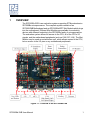
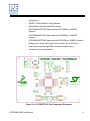
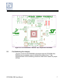
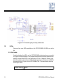
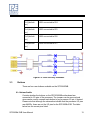
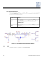
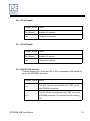
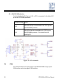
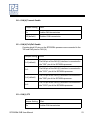
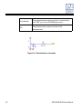
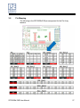
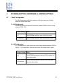
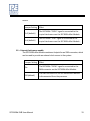
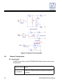
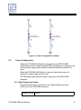
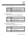
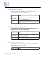
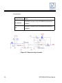
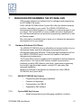
Purchase Agreement
P&E Microcomputer Systems, Inc. reserves the right to make changes without further notice to any
products herein to improve reliability, function, or design. P&E Microcomputer Systems, Inc. does not
assume any liability arising out of the application or use of any product or circuit described herein.
This software and accompanying documentation are protected by United States Copyright law and
also by International Treaty provisions. Any use of this software in violation of copyright law or the
terms of this agreement will be prosecuted.
All the software described in this document is copyrighted by P&E Microcomputer Systems, Inc.
Copyright notices have been included in the software.
P&E Microcomputer Systems authorizes you to make archival copies of the software and
documentation for the sole purpose of back-up and protecting your investment from loss. Under no
circumstances may you copy this software or documentation for the purpose of distribution to others.
Under no conditions may you remove the copyright notices from this software or documentation.
This software may be used by one person on as many computers as that person uses, provided that
the software is never used on two computers at the same time. P&E expects that group programming
projects making use of this software will purchase a copy of the software and documentation for each
user in the group. Contact P&E for volume discounts and site licensing agreements.
P&E Microcomputer Systems does not assume any liability for the use of this software beyond the
original purchase price of the software. In no event will P&E Microcomputer Systems be liable for
additional damages, including any lost profits, lost savings or other incidental or consequential
damages arising out of the use or inability to use these programs, even if P&E Microcomputer Systems
has been advised of the possibility of such damage.
By using this software, you accept the terms of this agreement.
© 2008 P&E Microcomputer Systems, Inc. “MS-DOS” and “Windows” are registered trademarks of
Microsoft Corporation. “PowerPC” is a registered trademark of IBM corporation.
P&E Microcomputer Systems, Inc.
P.O. Box 2044
Woburn, MA 01888
617-923-0053
http://www.pemicro.com
Manual version 1.00
1
2
3
4
5
6
OVERVIEW..................................................................................................... 1
1.1
Package Contents .......................................................................................... 2
1.2
Supported Devices ......................................................................................... 2
1.3
Recommended Materials ............................................................................... 2
1.4
Handling Precautions ..................................................................................... 3
HARDWARE FEATURES............................................................................... 3
2.1
SPC56XXMB Board Features ........................................................................ 3
2.2
SPC560BxADPT Mini-Module Board Features.............................................. 4
2.3
Pin Numbering for Jumpers............................................................................ 7
SPC56XXMB HARDWARE & JUMPER SETTINGS ...................................... 9
3.1
Power Supplies .............................................................................................. 9
3.2
LEDs............................................................................................................. 12
3.3
Buttons ......................................................................................................... 13
3.4
LIN................................................................................................................ 15
3.5
SCI ............................................................................................................... 20
3.6
CAN.............................................................................................................. 22
3.7
Potentiometer ............................................................................................... 25
3.8
Pin Mapping ................................................................................................. 27
SPC560BxADPT100S HARDWARE & JUMPER SETTINGS ...................... 29
4.1
Boot Configuration........................................................................................ 29
4.2
Power Configuration..................................................................................... 30
4.3
System Clock Configuration ......................................................................... 32
4.4
General Configuration .................................................................................. 34
SPC560BxADPT144S HARDWARE & JUMPER SETTINGS ...................... 36
5.1
Boot Configuration........................................................................................ 36
5.2
Power Configuration..................................................................................... 37
5.3
System Clock Configuration ......................................................................... 38
5.4
General Configuration .................................................................................. 41
SPC560BxADPT208S HARDWARE & JUMPER SETTINGS ...................... 42
6.1
Boot Configuration........................................................................................ 42
6.2
Power Configuration..................................................................................... 43
SPC560Bx EVB User Manual
ii
7
iii
6.3
System Clock Configuration .........................................................................47
6.4
General Configuration...................................................................................49
DEBUGGING/PROGRAMMING THE SPC560Bx EVB ................................ 51
7.1
Hardware Solutions At A Glance ..................................................................51
7.2
Working With P&E’s USB-ML-PPCNEXUS .................................................52
7.3
Working With P&E’s Cyclone MAX ...............................................................53
SPC560Bx EVB User Manual
1
OVERVIEW
The SPC560Bx EVB is an evaluation system supporting STMicroelectronics
SPC560Bx microprocessors. The complete system consists of an
SPC56XXMB Motherboard and an SPC560BxADPT Mini-Module which plugs
into the motherboard. Different Mini-Modules are available for evaluating
devices with different footprints in the SPC560Bx family of microprocessors.
The evaluation system allows full access to the CPU, all of the CPU’s I/O
signals, and the motherboard peripherals (such as CAN, SCI, LIN). The MiniModule may be used as a stand-alone unit, which allows access to the CPU,
but no access to the I/O pins or any motherboard peripherals.
Figure 1-1: Overview of the SPC560Bx EVB
SPC560Bx EVB User Manual
1
1.1
Package Contents
An SPC560Bx Evaluation Kit includes the following items:
•
One SPC56XXMB Motherboard
•
One SPC560BxADPT100S or SPC560BxADPT144S or
SPC560BxADPT208S Mini-Module
•
One SPC56XX Resources CD-ROM
•
One P&E USB-ML-PPCNEXUS Hardware Interface Cable
•
One USB A-to-B Cable
•
STMicroelectronics Warranty Card
An SPC560Bx Adapter Package includes the following items:
1.2
•
One SPC560BxADPT100S or SPC560BxADPT144S or
SPC560BxADPT208S Mini-Module
•
One SPC56XX Resources CD-ROM
•
STMicroelectronics Warranty Card
Supported Devices
The SPC560BxADPT100S Mini-Module supports the following devices:
•
SPC560BxxL3 (100LQFP)
The SPC560BxADPT144S Mini-Module supports the following devices:
•
SPC560BxxL5 (144LQFP)
The SPC560BxADPT208S Mini-Module supports the following devices:
•
1.3
2
SPC560BxxB2 (208BGA)
Recommended Materials
•
STMicroelectronics MPC5604B reference manual and datasheet
•
SPC56XXMB schematic
•
SPC560BxADPT100S schematic
•
SPC560BxADPT144S schematic
•
SPC560BxADPT208S schematic
SPC560Bx EVB User Manual
1.4
Handling Precautions
Please take care to handle the package contents in a manner such as to
prevent electrostatic discharge.
2
HARDWARE FEATURES
The SPC560Bx EVB is an evaluation system for STMicroelectronics’
SPC560Bx microprocessors. A 38-pin Mictor Nexus port and/or a 14-pin
JTAG port are provided on the Mini-Module to allow usage of an external
PowerPC Nexus interface such as P&E USB-ML-PPCNEXUS cable and
Cyclone MAX automated programmer.
2.1
SPC56XXMB Board Features
•
ON/OFF Power Switch w/ LED indicators
•
A 12VDC power supply input barrel connector
•
Onboard ST Microelectronics L9758 regulator provides three different
power voltages simultaneously: 5V, 3.3V, and 1.2V
•
Onboard peripherals can be configured to operate at 5V or 3.3V logic
levels
•
Two CAN channels with jumper enables
•
•
•
One CAN channel with High-Speed transceiver and DB9 male
connector
•
One CAN channel with Low-Speed Fault Tolerant and HighSpeed transceiver (selectable with jumpers) and DB9 male
connector
Two LIN channels with jumper enables
•
One channel with transceiver and pin header connector
populated
•
One channel with footprints only
One SCI channel with jumper enables
•
•
Transceiver with DB9 female connector
Two FlexRay channels with jumper enables
SPC560Bx EVB User Manual
3
•
One channel with transceiver and DB9 male connector
•
One channel with footprint only
•
Four user push buttons with jumper enables and polarity selection
•
Four user LED’s with jumper enables
•
One potentiometer for analog voltage input
•
Pin array for accessing all I/O signals
•
Expansion connectors for accessing all I/O signals
•
Development zone with 0.1” spacing and SOIC footprint prototyping
•
Specifications:
•
Board Size 5.5” x 9.0”
•
12VDC Center Positive power supply with 2.5/5.5mm barrel
connector
Figure 2-1: SPC56XXMB Top Component Placement
2.2
SPC560BxADPT Mini-Module Board Features
•
4
Can be used as a stand-alone board by providing external 5V power
SPC560Bx EVB User Manual
supply input
•
ON/OFF Power Switch w/ LED indicator
•
Reset button with filter and LED indicator
•
SPC560BxADPT100S has socket for SPC560Bx in 100LQFP
footprint
•
SPC560BxADPT144S has socket for SPC560Bx in 144LQFP
footprint
•
SPC560BxADPT208S has socket for SPC560Bx in 208BGA footprint
•
Debug ports: 38-pin Mictor Nexus port and/or 14-pin JTAG port
•
Direct clock input through SMA connector (footprint only)
•
Jumpers for boot configuration
Figure 2-2: xPC560PT100S Top Component Placement
SPC560Bx EVB User Manual
5
Figure 2-3: SPC560BxADPT144S Top Component Placement
6
SPC560Bx EVB User Manual
Figure 2-4: SPC560BxADPT208BGA Top Component Placement
2.3
Pin Numbering for Jumpers
Jumpers for both the SPC56XXMB motherboard and the SPC560Bx MiniModules have a rounded corner to indicate the position of pin 1. See
examples below for the numbering convention used in this manual for jumper
settings.
SPC560Bx EVB User Manual
7
Figure 2-5: Pin Numbering
8
SPC560Bx EVB User Manual
3
3.1
SPC56XXMB HARDWARE & JUMPER SETTINGS
Power Supplies
The SPC56XXMB obtains its power from the 12VDC Center Positive input
barrel connector. The following jumpers are used to configure the power
supply output:
J3 – VSA Tracking Regulator Configuration
Jumper Setting
Effect
On
The ST L9758 tracking regulator VSA tracks the input voltage at its TRACK_REF pin.
Off (default)
The ST L9758 tracking regulator VSA tracks 5V
J4 – VPROG Regulators Control
Jumper Setting
Position
On
1+2
3+4
SPC560Bx EVB User Manual
Effect
VKAM regulator output is programmed to 1V
Off (default)
VKAM regulator output is programmed to 1.5V
On
VSTBY regulator output is programmed to 2.6V
Off (default)
VSTBY regulator output is programmed to 3.3V
9
5+6
On
VDLL regulator output is programmed to 2.6V
Off (default)
VDLL regulator output is programmed to 3.3V
J5 – Regulators Enable & Standby
Jumper Setting
Position
On
1+2
Off (default)
Effect
The power regulator is always on
The power regulator is in standby if jumpers 5+6 are also in the “off” position
On
VSB, VSC, and VSD tracking regulators are disabled
Off (default)
VSB, VSC, and VSD tracking regulators are enabled
On (default)
The power regulator is always on
3+4
5+6
7+8
10
Off
The power regulator is in standby if jumpers 1+2 are also in the “off” position
On
VDLL and VCORE regulators are disabled
Off (default)
VDLL and VCORE regulators are enabled
SPC560Bx EVB User Manual
J36 – VIO Peripherals Logic Level
Jumper Setting
Effect
1+2
Onboard peripherals are configured for 3.3V logic
2+3 (default)
Onboard peripherals are configured for 5V logic
J37 – VBat low voltage detection
Jumper Setting
Effect
On
Low battery detection is enabled
Off (default)
Low battery detection is disabled
SPC560Bx EVB User Manual
11
Figure 3-1: Power Supply circuitry schematic
3.2
LEDs
There are four user LEDs available on the SPC56XXMB. All LEDs are active
low.
J7 – LEDs Enable
Controls whether the LEDs on the SPC56XXMB motherboard are connected
to I/O pins of the processor. The jumpers can be removed and wires can be
used to connect each LED to any processor I/O pin, if desired. Please note
that although the schematics indicate that the processor I/O pins are eMIOSx,
those are not the I/O pins for the SPC560Bx EVB. The table below has the
correct pins listed.
Jumper Setting
12
Effect
SPC560Bx EVB User Manual
1+2 (default on)
LED1 connected to PE4
3+4 (default on)
LED2 connected to PE5
5+6 (default on)
LED3 connected to PE6
7+8 (default on)
LED4 connected to PE7
Figure 3-2: LEDs circuitry schematic
3.3
Buttons
There are four user buttons available on the SPC56XXMB.
J8 – Buttons Enable
Controls whether the buttons on the SPC56XXMB motherboard are
connected to I/O pins of the processor. The jumpers can be removed and
wires can be used to connect each button to any processor I/O pin, if desired.
Please note that although the schematics indicate that the processor I/O pins
are eMIOSx, those are not the I/O pins for the SPC560Bx EVB. The table
below has the correct pins listed.
SPC560Bx EVB User Manual
13
Jumper Setting
Effect
1+2 (default on)
KEY1 connected to PE0
3+4 (default on)
KEY2 connected to PE1
5+6 (default on)
KEY3 connected to PE2
7+8 (default on)
KEY4 connected to PE3
J9 – Buttons Driving Configuration
Selects whether the buttons drive logic high or drive logic low when pressed.
14
Jumper Setting
Effect
1+2
When pressed, buttons will send logic high to the connected I/O pin
2+3 (default)
When pressed, buttons will send logic low to the connected I/O pin
SPC560Bx EVB User Manual
J40 – Buttons Idle Configuration
Selects whether the I/O pins are pulled logic high or pulled logic low. This
controls the defaultlogic level of the I/O pins when the buttons are not
pressed.
Jumper Setting
Effect
1+2 (default)
I/O pins connected to the buttons are pulled up to logic high
2+3
I/O pins connected to the buttons are pulled down to logic low
Figure 3-3: Buttons circuitry schematic
3.4
LIN
There are footprints for two LIN connections on the SPC56XXMB. By default,
SPC560Bx EVB User Manual
15
one LIN circuit is assembled (LIN1) and the other circuit is left unpopulated
(LIN2).
J6 – LIN1 pin2 configuration
Jumper Setting
Effect
On
Pin 2 of the LIN1 connector is connected to 12V
Off (default)
Pin 2 of the LIN1 connector is not connected to 12V
J22 – LIN1 enable
Jumper Setting
Effect
On (default)
Enables the LIN1 transceiver
Off
Disables the LIN1 transceiver
J23 – LIN1 master selection
16
Jumper Setting
Effect
On LIN1 is configured as a master node
Off (default)
LIN1 is configured as a slave node
SPC560Bx EVB User Manual
J24 – LIN1 pin1 configuration
Jumper Setting
Effect
On Pin 1 of the LIN1 connector is connected to 12V
Off (default)
Pin 1 of the LIN1 connector is not connected to 12V
J27 – LIN1/SCI TxD selection
Controls whether the TxD pin on LIN1 or SCI is connected to the default I/O
pin on the SPC560Bx processor.
Jumper Setting
Effect
1+2
The LIN1 TxD pin is connected to the “PB2” pin on the SPC560Bx processor. This should be set if enabling LIN1.
2+3
The SCI TxD pin is connected to the “PB2” pin on the SPC560Bx processor.
J28 – LIN1/SCI RxD selection
Controls whether the RxD pin on LIN1 or SCI is connected to the default I/O
pin on the SPC560Bx processor.
Jumper Setting
Effect
1+2
The LIN1 RxD pin is connected to the “PB3” pin on the SPC560Bx processor. This should be set if enabling LIN1.
SPC560Bx EVB User Manual
17
2+3
The SCI RxD pin is connected to the “PB3” pin on the SPC560Bx processor.
Figure 3-4: LIN1 Schematic
J31 – LIN2 pin2 configuration
Jumper Setting
Effect
On
Pin 2 of the LIN2 connector is connected to 12V
Off (default)
Pin 2 of the LIN2 connector is not connected to 12V
J19 – LIN2 enable
Jumper Setting Effect
18
On
Enables the LIN2 transceiver
Off (default)
Disables the LIN2 transceiver
SPC560Bx EVB User Manual
J20 – LIN2 master selection
Jumper Setting
Effect
On LIN2 is configured as a master node
Off (default)
LIN2 is configured as a slave node
J21 – LIN2 pin1 configuration
Jumper Setting
Effect
On Pin 1 of the LIN2 connector is connected to 12V
Off (default)
Pin 1 of the LIN2 connector is not connected to 12V
J29 – LIN2/SCI TxD selection
Controls whether the TxD pin on LIN2 or SCI is connected to the default I/O
pin on the SPC560Bx processor.
Jumper Setting
Effect
1+2
The LIN2 TxD pin is connected to the “PC6” pin on the SPC560Bx processor. This should be set if enabling LIN2.
2+3
The SCI TxD pin is connected to the “PC6” pin on the SPC560Bx processor.
SPC560Bx EVB User Manual
19
J30 – LIN2/SCI RxD selection
Controls whether the RxD pin on LIN2 or SCI is connected to the default I/O
pin on the SPC560Bx processor.
Jumper Setting
Effect
1+2
The LIN2 RxD pin is connected to the “PC7” pin on the SPC560Bx processor. This should be set if enabling LIN2.
2+3
The SCI RxD pin is connected to the “PC7” pin on the SPC560Bx processor.
Figure 3-5: LIN2 schematic (Not populated by default)
3.5
SCI
One SCI interface is available on the SPC56XXMB.
20
SPC560Bx EVB User Manual
J16 – SCI TxD Enable
Jumper Setting
Effect
On (default)
Enables SCI transmit
Off
Disables SCI transmit
J17 – SCI RxD Enable
Jumper Setting
Effect
On (default)
Enables SCI receive
Off
Disables SCI receive
J27 – LIN1/SCI TxD selection
Controls whether the TxD pin on LIN1 or SCI is connected to the default I/O
pin on the SPC560Bx processor.
Jumper Setting
Effect
1+2
The LIN1 TxD pin is connected to the “PB2” pin on the SPC560Bx processor.
2+3
The SCI TxD pin is connected to the “PB2” pin on the SPC560Bx processor. This should be set if enabling SCI.
SPC560Bx EVB User Manual
21
J28 – LIN1/SCI RxD selection
Controls whether the RxD pin on LIN1 or SCI is connected to the default I/O
pin on the SPC560Bx processor.
Jumper Setting
Effect
1+2
The LIN1 RxD pin is connected to the “PB3” pin on the SPC560Bx processor.
2+3
The SCI RxD pin is connected to the “PB3” pin on the SPC560Bx processor. This should be set if enabling SCI.
Figure 3-6: SCI schematic
3.6
CAN
Two CAN interfaces are implemented on the SPC56XXMB: a high-speed
CAN interface and a low-speed CAN interface.
22
SPC560Bx EVB User Manual
J14 – CAN (H) Transmit Enable
Jumper Setting
Effect
On
Enables CAN transmission
Off (default)
Disables CAN transmission
J15 – CAN (H) TxD/RxD Enable
Controls which I/O pins on the SPC560Bx processor are connected to the
TxD and RxD pins on CAN (H).
Jumper Setting
Effect
1+3 (default)
The RxD pin of the CAN (H) interface is connected to the “PB1” pin of the SPC560Bx processor.
3+5
The RxD pin of the CAN (H) interface is connected to the “PC11” pin of the SPC560Bx processor.
2+4 (default)
The TxD pin of the CAN (H) interface is connected to the “PB0” pin of the SPC560Bx processor.
4+6
The TxD pin of the CAN (H) interface is connected to the “PC10” pin of the SPC560Bx processor.
J13 – CAN (L) CTE
Jumper Setting Effect
On
SPC560Bx EVB User Manual
Enables CAN transmission
23
Off (default)
Disables CAN transmission
J11 – CAN (L) TxD/RxD Enable
Controls which I/O pins on the SPC560Bx processor are connected to the
TxD and RxD pins on CAN (L).
24
Jumper Setting
Effect
1+3
The RxD pin of the CAN (L) interface is connected to the “PB1” pin of the SPC560Bx processor.
3+5 (default)
The RxD pin of the CAN (L) interface is connected to the “PC11” pin of the SPC560Bx processor.
2+4
The TxD pin of the CAN (L) interface is connected to the “PB0” pin of the SPC560Bx processor.
4+6 (default)
The TxD pin of the CAN (L) interface is connected to the “PC10” pin of the SPC560Bx processor.
SPC560Bx EVB User Manual
Figure 3-7: High Speed CAN schematic
Figure 3-8: Low Speed CAN schematic
3.7
Potentiometer
A potentiometer is available on the SPC56XXMB to allow an analog voltage
input.
J18 – POT Enable
Jumper Setting
SPC560Bx EVB User Manual
Effect
25
On (default)
The potentiometer wiper terminal is connected to the “PB0” pin on the SPC560Bx processor.
Off
The potentiometer wiper terminal is left disconnected.
Figure 3-9: Potentiometer schematic
26
SPC560Bx EVB User Manual
3.8
Pin Mapping
The following is the SPC560Bx EVB pin assignment for the Pin Array
headers:
SPC560Bx EVB User Manual
27
Figure 3-10: Pin Mapping
28
SPC560Bx EVB User Manual
4
4.1
SPC560BxADPT100S HARDWARE & JUMPER SETTINGS
Boot Configuration
The following jumpers affect the operation of the processor as it initially
comes out of the reset state:
J7 – FAB Configuration
Controls whether the processor boots from internal FLASH or from a serial
interface (CAN, SCI)
Jumper Setting
Effect
1+2
The SPC560Bx processor uses serial boot mode
2+3 (default)
The SPC560Bx processor uses internal boot mode
J8 – ABS Configuration
If J7 is configured for serial boot mode, this jumper selects between UART or
CAN. If J7 is configured for internal boot mode, this jumper has no effect.
Jumper Setting
Effect
1+2 The SPC560Bx processor uses the CAN interface for serial boot mode
2+3 (default)
The SPC560Bx processor uses the UART interface for serial boot mode
SPC560Bx EVB User Manual
29
Figure 4-1: Boot Configuration Jumpers
4.2
Power Configuration
When the SPC560Bx Mini-Module is plugged into the SPC56XXMB
motherboard, power is supplied directly by the motherboard. In this setup, the
external power supply input available on the Mini-Module should NOT be
used.
When the SPC560Bx Mini-Module is used as a stand-alone board, an
external 5V power supply must be used.
The following jumpers affect the power supply pins of the SPC560Bx
processor:
J14 – Digital Supply Input Enable
Controls whether power is provided to the “Digital Supply Input” pins
(VDD_HV) on the SPC560Bx processor.
Jumper Setting
30
Effect
SPC560Bx EVB User Manual
On (default)
SPC560Bx Digital Supply Input pins are connected to 5V
Off
SPC560Bx Digital Supply Input pins are unpowered
J15 – 1.2V Decoupling Pins Configuration
Controls whether the 1.2V decoupling pins (VDD_LV) on the SPC560Bx
processor are connected to 1.2V power.
Jumper Setting
Effect
On SPC560Bx 1.2V decoupling pins are connected to 1.2V
Off (default)
SPC560Bx 1.2V decoupling pins are connected only to decoupling capacitors
SPC560Bx EVB User Manual
31
J16 – Internal Regulator Supply Configuration
Controls whether the “internal regulator supply” pin (VDD_BV) on the
SPC560Bx processor are connected to 5V power.
4.3
Jumper Setting
Effect
1+2 (default)
SPC560Bx internal regulator supply pin is connected to 5V
2+3
SPC560Bx internal regulator supply pin is connected to GND
System Clock Configuration
The SPC560Bx Mini-Modules support the usage of crystal clock sources as
well as external clock sources.
J3 – 32KHz Clock Enable
Both of the jumpers below need to be installed to enable the 32 KHz crystal
clock source
Jumper Setting
Effect
1+2 (default)
The SPC560Bx “OSC32K_EXTAL” signal is connected to the 32KHz crystal clock source on the SPC560Bx Mini‐Module
3+4 (default)
The SPC560Bx “OSC32K_XTAL” signal is connected to the 32KHz crystal clock source on the SPC560Bx Mini‐Module
J10 – Crystal clock source enable
Both of the jumpers below need to be installed to enable the crystal clock
32
SPC560Bx EVB User Manual
source.
Jumper Setting
Effect
1+2 (default)
The SPC560Bx “EXTAL” signal is connected to the crystal clock source on the SPC560Bx Mini‐Module
3+4 (default)
The SPC560Bx “XTAL” signal is connected to the crystal clock source on the SPC560Bx Mini‐Module
J11 – External clock source enable
The SPC560Bx Mini-Module contains a footprint for an SMA connector, which
can be used to provide an external clock source to the system.
Jumper Setting
Effect
On
The SPC560Bx “EXTAL” signal is connected to the SMA connector on the SPC560Bx Mini‐Module
Off (default)
The SMA connector on the SPC560Bx Mini‐Module is disconnected from the processor
SPC560Bx EVB User Manual
33
Figure 4-2: System Clock schematic
4.4
General Configuration
J13 – Reset Enable
A RESET push button on the SPC560Bx Mini-Module can be used to reset
the processor.
Jumper Setting Effect
On (default)
34
The RESET button on the SPC560Bx Mini‐Module is enabled
SPC560Bx EVB User Manual
Off
The RESET button on the SPC560Bx Mini‐Module is disabled
Figure 4-3: Reset circuitry schematic
SPC560Bx EVB User Manual
35
5
5.1
SPC560BxADPT144S HARDWARE & JUMPER SETTINGS
Boot Configuration
The following jumpers affect the operation of the processor as it initially
comes out of the reset state:
J7 – FAB Configuration
Controls whether the processor boots from internal FLASH or from a serial
interface (CAN, SCI)
Jumper Setting
Effect
1+2
The SPC560Bx processor uses serial boot mode
2+3 (default)
The SPC560Bx processor uses internal boot mode
J8 – ABS Configuration
If J7 is configured for serial boot mode, this jumper selects between UART or
CAN. If J7 is configured for internal boot mode, this jumper has no effect.
36
Jumper Setting
Effect
1+2 The SPC560Bx processor uses the CAN interface for serial boot mode
2+3 (default)
The SPC560Bx processor uses the UART interface for serial boot mode
SPC560Bx EVB User Manual
Figure 5-1: Boot Configuration Jumpers
5.2
Power Configuration
When the SPC560Bx Mini-Module is plugged into the SPC56XXMB
motherboard, power is supplied directly by the motherboard. In this setup, the
external power supply input available on the Mini-Module should NOT be
used.
When the SPC560Bx Mini-Module is used as a stand-alone board, an
external 5V power supply must be used.
The following jumpers affect the power supply pins of the SPC560Bx
processor:
J14 – Digital Supply Input Enable
Controls whether power is provided to the “Digital Supply Input” pins
(VDD_HV) on the SPC560Bx processor.
Jumper Setting
SPC560Bx EVB User Manual
Effect
37
On (default)
SPC560Bx Digital Supply Input pins are connected to 5V
Off
SPC560Bx Digital Supply Input pins are unpowered
J15 – 1.2V Decoupling Pins Configuration
Controls whether the 1.2V decoupling pins (VDD_LV) on the SPC560Bx
processor are connected to 1.2V power.
Jumper Setting
Effect
On SPC560Bx 1.2V decoupling pins are connected to 1.2V
Off (default)
SPC560Bx 1.2V decoupling pins are connected only to decoupling capacitors
J16 – Internal Regulator Supply Configuration
Controls whether the “internal regulator supply” pin (VDD_BV) on the
SPC560Bx processor are connected to 5V power.
5.3
38
Jumper Setting
Effect
1+2 (default)
SPC560Bx internal regulator supply pin is connected to 5V
2+3
SPC560Bx internal regulator supply pin is connected to GND
System Clock Configuration
SPC560Bx EVB User Manual
The SPC560Bx Mini-Modules support the usage of crystal clock sources as
well as external clock sources.
J3 – 32KHz Clock Enable
Both of the jumpers below need to be installed to enable the 32 KHz crystal
clock source
Jumper Setting
Effect
1+2 (default)
The SPC560Bx “OSC32K_EXTAL” signal is connected to the 32KHz crystal clock source on the SPC560Bx Mini‐Module
3+4 (default)
The SPC560Bx “OSC32K_XTAL” signal is connected to the 32KHz crystal clock source on the SPC560Bx Mini‐Module
J10 – Crystal clock source enable
Both of the jumpers below need to be installed to enable the crystal clock
source.
Jumper Setting
Effect
1+2 (default)
The SPC560Bx “EXTAL” signal is connected to the crystal clock source on the SPC560Bx Mini‐Module
3+4 (default)
The SPC560Bx “XTAL” signal is connected to the crystal clock source on the SPC560Bx Mini‐Module
J11 – External clock source enable
SPC560Bx EVB User Manual
39
The SPC560Bx Mini-Module contains a footprint for an SMA connector, which
can be used to provide an external clock source to the system.
40
Jumper Setting
Effect
On
The SPC560Bx “EXTAL” signal is connected to the SMA connector on the SPC560Bx Mini‐Module
Off (default)
The SMA connector on the SPC560Bx Mini‐Module is disconnected from the processor
SPC560Bx EVB User Manual
Figure 5-2: System Clock schematic
5.4
General Configuration
J13 – Reset Enable
A RESET push button on the SPC560Bx Mini-Module can be used to reset
the processor.
Jumper Setting
Effect
On (default)
The RESET button on the SPC560Bx Mini‐Module is enabled
Off
The RESET button on the SPC560Bx Mini‐Module is disabled
Figure 5-3: Reset circuitry schematic
SPC560Bx EVB User Manual
41
6
6.1
SPC560BxADPT208S HARDWARE & JUMPER SETTINGS
Boot Configuration
The following jumpers affect the operation of the processor as it initially
comes out of the reset state:
J7 – FAB Configuration
Controls whether the processor boots from internal FLASH or from a serial
interface (CAN, SCI)
Jumper Setting
Effect
1+2
The SPC560Bx processor uses serial boot mode
2+3 (default)
The SPC560Bx processor uses internal boot mode
J8 – ABS Configuration
If J7 is configured for serial boot mode, this jumper selects between UART or
CAN. If J7 is configured for internal boot mode, this jumper has no effect.
42
Jumper Setting
Effect
1+2 The SPC560Bx processor uses the CAN interface for serial boot mode
2+3 (default)
The SPC560Bx processor uses the UART interface for serial boot mode
SPC560Bx EVB User Manual
Figure 6-1: Boot Configuration Jumpers
6.2
Power Configuration
When the SPC560Bx Mini-Module is plugged into the SPC56XXMB
motherboard, power is supplied directly by the motherboard. In this setup, the
external power supply input available on the Mini-Module should NOT be
used.
When the SPC560Bx Mini-Module is used as a stand-alone board, an
external 5V or 3.3V power supply must be used. The SPC560BxADPT208S is
the only SPC560Bx Mini-Module that is able to accept both 5V and 3.3V for
input power when used as a stand-alone board.
The following jumpers affect the power supply pins of the SPC560Bx
processor:
J4 – Debug Port Voltage Configuration
Sets the logic voltage level on the 14-pin JTAG port and 38-pin MICTOR port
(if available). These ports are used by external interface hardware to
SPC560Bx EVB User Manual
43
communicate with the processor.
Jumper Setting
Effect
1+2 (default)
Debug port(s) are configured for 5V logic
2+3
Debug port(s) are configured for 3.3V logic
J14 – Digital Supply Input Enable
Controls whether power is provided to the “Digital Supply Input” pins
(VDD_HV - pins C2, E16, G13, H3, R5) on the SPC560Bx processor.
Jumper Setting
Effect
On (default)
SPC560Bx Digital Supply Input pins are connected to 3.3V or 5V (determined by J19)
Off
SPC560Bx Digital Supply Input pins are unpowered
J15 – Digital Supply Input OSC0REG0 Enable
Controls whether power is provided to the “Digital Supply Input” pins
(VDD_HV, pin N9) on the SPC560Bx processor.
44
Jumper Setting
Effect
On (default)
SPC560Bx Digital Supply Input pin N9 is connected to 3.3V or 5V (determined by J19)
Off
SPC560Bx Digital Supply Input pin N9 is unpowered
SPC560Bx EVB User Manual
J16 – Digital Supply Input FLA0 Enable
Controls whether power is provided to the “Digital Supply Input” pins
(VDD_HV – pin D9) on the SPC560Bx processor.
Jumper Setting
Effect
1+2 (default)
SPC560Bx Digital Supply Input pin D9 is connected to 3.3V or 5V (determined by J19)
2+3
SPC560Bx Digital Supply Input pin D9 is connected to GND
J17 – ADC Analog Supply Voltage Enable
Controls whether the reference voltage and analog supply pin for the A/D
converter (VDD_HV_ADC, pin P14) is powered.
Jumper Setting
Effect
On (default)
SPC560Bx ADC supply pin P14 is connected to 3.3V or 5V (determined by J19)
Off
SPC560Bx Digital Supply Input pin D9 is unpowered
J18 – 1.2V Decoupling Pins Configuration
Controls whether the 1.2V decoupling pins (VDD_LV) on the SPC560Bx
processor are connected to 1.2V power.
Jumper Setting
SPC560Bx EVB User Manual
Effect
45
On SPC560Bx 1.2V decoupling pins are connected to 1.2V
Off (default)
SPC560Bx 1.2V decoupling pins are connected only to decoupling capacitors
J19 – Power Supply Voltage Selection
Controls whether the processor is powered using 5V or 3.3V. This selection
can only be made if the SPC560Bx Mini-Module is plugged into the
SPC56XXMB motherboard. If the SPC560Bx Mini-Module is used as a standalone board, the processor is powered directly by the external power supply
and this jumper setting has no effect.
Jumper Setting
Effect
1+2 (default)
SPC560Bx processor is powered by the 5V supply
2+3
SPC560Bx processor is powered by the 3.3V supply
J20 – Internal Regulator Supply Configuration
Controls whether the “internal regulator supply” pin (VDD_BV) on the
SPC560Bx processor is powered.
46
Jumper Setting
Effect
1+2 (default)
SPC560Bx internal regulator supply pin is connected to 5V or 3.3V (determined by J19)
2+3
SPC560Bx internal regulator supply pin is connected to GND
SPC560Bx EVB User Manual
6.3
System Clock Configuration
The SPC560Bx Mini-Modules support the usage of crystal clock sources as
well as external clock sources.
J3 – 32KHz Clock Enable
Both of the jumpers below need to be installed to enable the 32 KHz crystal
clock source
Jumper Setting
Effect
1+2 (default)
The SPC560Bx “OSC32K_XTAL” signal is connected to the 32KHz crystal clock source on the SPC560Bx Mini‐Module
3+4 (default)
The SPC560Bx “OSC32K_EXTAL” signal is connected to the 32KHz crystal clock source on the SPC560Bx Mini‐Module
J10 – Crystal clock source enable
Both of the jumpers below need to be installed to enable the crystal clock
source.
Jumper Setting
Effect
1+2 (default)
The SPC560Bx “EXTAL” signal is connected to the crystal clock source on the SPC560Bx Mini‐Module
3+4 (default)
The SPC560Bx “XTAL” signal is connected to the crystal clock source on the SPC560Bx Mini‐Module
SPC560Bx EVB User Manual
47
J11 – External clock source enable
The SPC560Bx Mini-Module contains a footprint for an SMA connector, which
can be used to provide an external clock source to the system.
48
Jumper Setting
Effect
On
The SPC560Bx “EXTAL” signal is connected to the SMA connector on the SPC560Bx Mini‐Module
Off (default)
The SMA connector on the SPC560Bx Mini‐Module is disconnected from the processor
SPC560Bx EVB User Manual
Figure 6-2: System Clock schematic
6.4
General Configuration
J13 – Reset Enable
A RESET push button on the SPC560Bx Mini-Module can be used to reset
SPC560Bx EVB User Manual
49
the processor.
Jumper Setting
Effect
On (default)
The RESET button on the SPC560Bx Mini‐Module is enabled
Off
The RESET button on the SPC560Bx Mini‐Module is disabled
Figure 6-3: Reset circuitry schematic
50
SPC560Bx EVB User Manual
7
DEBUGGING/PROGRAMMING THE SPC560Bx EVB
P&E provides hardware and software tools for debugging and programming
the SPC560Bx EVB system.
P&E’s USB-ML-PPCNEXUS and Cyclone MAX offer two effective hardware
solutions, depending on your needs. The USB-ML-PPCNEXUS is a
development tool that will enable you to debug your code and program it onto
your target. The Cyclone MAX is a more versatile and robust development
tool with advanced features and production programming capabilities, as well
as Ethernet support.
More information is available below to assist you in choosing the appropriate
development tool for your needs.
7.1
Hardware Solutions At A Glance
The USB-ML-PPCNEXUS offers an affordable and compact solution for your
development needs, and allows debugging and programming to be
accomplished simply and efficiently. Those doing rapid development will find
the USB-ML-PPCNEXUS easy to use and fully capable of fast-paced
debugging and programming.
The Cyclone MAX is a more complete solution designed for both development
and production. The Cyclone MAX features multiple communications
interfaces (including USB, Ethernet, and Serial), stand-alone programming
functionality, high speed data transfer, a status LCD, and many other
advanced capabilities.
Below is an overview of the features and intended use of the USB-MLPPCNEXUS and Cyclone MAX.
7.1.1
7.1.2
USB-ML-PPCNEXUS Key Features
•
Programming and debugging capabilities
•
Compact and lightweight
•
Communication via USB 2.0
•
Supported by P&E software
Cyclone MAX Key Features
•
Advanced programming and debugging capabilities, including:
SPC560Bx EVB User Manual
51
7.2
•
PC-Controlled and User-Controlled Stand-Alone Operation
•
Interactive Programming via Host PC
•
In-Circuit Debugging, Programming, and Testing
•
Supports STMicroelectronics’ SPC56xx microcontrollers
•
Communication via USB, Serial, and Ethernet Ports
•
Multiple image storage
•
LCD screen menu interface
•
Supported by P&E software
•
Works With P&E’s USB-ML-PPCNEXUS
Working With P&E’s USB-ML-PPCNEXUS
Figure 7-1: P&E’s USB-ML-PPCNEXUS
7.2.1
Product Features & Implementation
P&E’s USB-ML-PPCNEXUS Interface (USB-ML-PPCNEXUS) connects your
target to your PC and allows the PC access to the debug mode on
STMicroelectronics’ SPC56xx microcontrollers. It connects between a USB
port on a Windows 2000/XP/2003/Vista machine and a standard 14-pin JTAG/
Nexus connector on the target.
By using the USB-ML-PPCNEXUS Interface, the user can take advantage of
the background debug mode to halt normal processor execution and use a
PC to control the processor. The user can then directly control the target’s
execution, read/write registers and memory values, debug code on the
processor, and program internal or external FLASH memory devices. The
USB-ML-PPCNEXUS enables you to debug, program, and test your code on
your board.
52
SPC560Bx EVB User Manual
7.2.2
Software
The USB-ML-PPCNEXUS Interface works with P&E’s in-circuit debugger and
flash programmer to allow debug and flash programming of the target
processor. P&E’s USB-ML-PPCNEXUS Development Packages come with
the USB-ML-PPCNEXUS Interface, as well as flash programming software,
in-circuit debugging software, Windows IDE, and register file editor.
7.3
Working With P&E’s Cyclone MAX
Figure 7-2: P&E’s Cyclone MAX
7.3.1
Product Features & Implementation
P&E’s Cyclone MAX is an extremely flexible tool designed for debugging,
testing, and in-circuit flash programming of STMicroelectronics’ SPC56xx
microcontrollers. The Cyclone MAX connects your target to the PC via USB,
Ethernet, or Serial Port and enables you to debug your code, program, and
test it on your board. After development is complete the Cyclone MAX can be
used as a production tool on your manufacturing floor.
For production, the Cyclone MAX may be operated interactively via Windowsbased programming applications as well as under batch or .dll commands
from a PC. Once loaded with data by a PC it can be disconnected and
operated manually in a stand-alone mode via the LCD menu and control
buttons. The Cyclone MAX has over 3Mbytes of non-volatile memory, which
allows the on-board storage of multiple programming images. When
connected to a PC for programming or loading it can communicate via the
Ethernet, USB, or serial interfaces.
7.3.2
Software
The Cyclone MAX comes with intuitive configuration software and interactive
SPC560Bx EVB User Manual
53
programming software, as well as easy to use automated control software.
The Cyclone MAX also functions as a full-featured debug interface, and is
supported by development software from P&E.
P&E’s Cyclone MAX is also available bundled with additional software as part
of various Development Packages. In addition to the Cyclone MAX, these
Development Packages include in-circuit debugging software, flash
programming software, a Windows IDE, and register file editor.
54
SPC560Bx EVB User Manual