1
Virtex-4 RocketIO
Multi-Gigabit
Transceiver
User Guide
UG076 (v4.1) November 2, 2008
R
R
Xilinx is disclosing this user guide, manual, release note, and/or specification (the "Documentation") to you solely for use in the development
of designs to operate with Xilinx hardware devices. You may not reproduce, distribute, republish, download, display, post, or transmit the
Documentation in any form or by any means including, but not limited to, electronic, mechanical, photocopying, recording, or otherwise,
without the prior written consent of Xilinx. Xilinx expressly disclaims any liability arising out of your use of the Documentation. Xilinx reserves
the right, at its sole discretion, to change the Documentation without notice at any time. Xilinx assumes no obligation to correct any errors
contained in the Documentation, or to advise you of any corrections or updates. Xilinx expressly disclaims any liability in connection with
technical support or assistance that may be provided to you in connection with the Information.
THE DOCUMENTATION IS DISCLOSED TO YOU “AS-IS” WITH NO WARRANTY OF ANY KIND. XILINX MAKES NO OTHER
WARRANTIES, WHETHER EXPRESS, IMPLIED, OR STATUTORY, REGARDING THE DOCUMENTATION, INCLUDING ANY
WARRANTIES OF MERCHANTABILITY, FITNESS FOR A PARTICULAR PURPOSE, OR NONINFRINGEMENT OF THIRD-PARTY
RIGHTS. IN NO EVENT WILL XILINX BE LIABLE FOR ANY CONSEQUENTIAL, INDIRECT, EXEMPLARY, SPECIAL, OR INCIDENTAL
DAMAGES, INCLUDING ANY LOSS OF DATA OR LOST PROFITS, ARISING FROM YOUR USE OF THE DOCUMENTATION.
© 2005–2008 Xilinx, Inc. XILINX, the Xilinx logo, Virtex, Spartan, ISE, and other designated brands included herein are trademarks of Xilinx
in the United States and other countries. All other trademarks are the property of their respective owners.
Virtex-4 RocketIO MGT User Guide
www.xilinx.com
UG076 (v4.1) November 2, 2008
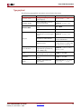
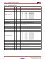
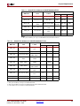
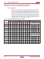
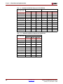
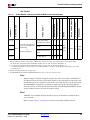
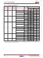
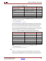
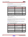
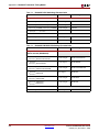
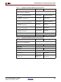
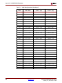
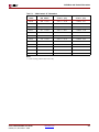
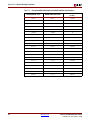
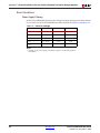
Revision History
The following table shows the revision history for this document.
Date
Version
Revision
03/01/05
1.0
Xilinx Initial Release.
03/10/05
1.1
Modified “Power Supply Requirements” in Chapter 6 and Table 6-1, page 176.
04/07/05
1.2
General typographical edits. Revised Table 2-2, Table 2-8, Figure 2-7, Figure 2-8,
Figure 2-11, Figure 2-12, Figure 6-4, Figure 6-8, and Figure E-2. Added “Resetting the
Transceiver,” page 85 and Figure 2-12. Edited Table 4-1, Table 4-3, Table 4-5, Table 7-3,
Table 7-4, Table 7-5, Table 7-6, Table A-1, Table C-14, and Table C-28.
07/01/05
1.3
Changes in Figure 2-4, Figure 2-9, Figure 3-14, Figure 4-9, Figure 6-4 and Figure 6-8.
Revised Table 3-23 and Table 3-24. Added Table 5-5, revised Table 5-5. Changes to
Table 7-4, Table 7-5, Table 7-6. For clarity, revised all the notes in the tables in
Appendix C. Added a default value to DCDR_FILTER in Appendix F.
01/16/06
2.0
Major revision. All material completely revised and updated, substantial new material
added.
05/23/06
3.0
Major revision. Chapter 1: All Ports/Attributes tables reviewed and expanded. Chapter
2: New Reset section. Low-latency material removed. Chapter 8: New. Chapters 9-12
(Section II): New.
07/19/06
3.1
• Table 1-3: Corrected maximum reference clock frequency to 644 MHz for Aurora
protocols.
• Table 1-11: Deleted instruction to set TXTERMTRIM to 0000.
• Chapter 2, section “Resetting the Transceiver”:
♦ Modified all references to LOCKUPDATE cycles to REFCLK cycles.
♦ Corrected state definitions in all flowcharts.
• Chapter 3, section “Channel Bonding”: Rewritten and enlarged.
• Chapter 8, section “RXSYNC”:
♦ Modified all references to LOCKUPDATE cycles to REFCLK cycles.
•
09/29/06
3.2
UG076 (v4.1) November 2, 2008
Table C-6 and Table C-19: Corrected TXTERMTRIM default state to 1100.
• Removed references to the FF1760 package. Not supported.
• Removed references to 1-byte and 2-byte external fabric widths for PCS Bypass mode.
Not supported.
• Removed references to OC-48 protocol. Not supported.
• Removed references to Digital ReceiverLoopback. Not supported.
• Removed former Tables 4-6, 4-7, and Figure 4-12 from section “Out-of-Band (OOB)
Signals.”
• Added RX/TXFDCAL_CLOCK_DIVIDE setting of FOUR for RX/TX calibration with
reference clock speeds over 500 MHz (Table 4-4, Table 4-5).
• Added in several places throughout the Guide the recommendation to use the
RocketIO Wizard for MGT configuration.
• Added several new sections and diagrams to Chapter 6, “Analog and Board Design
Considerations” relating to powering MGTs. Existing material edited and updated.
• Added new section “SelectIO-to-MGT Crosstalk”to Chapter 6, “Analog and Board
Design Considerations.”
• Added Appendix D, “Special Analog Functions.” Previously part of Chapter 4.
www.xilinx.com
Virtex-4 RocketIO MGT User Guide
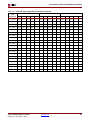
Date
Version
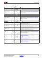
08/17/07
4.0
Revision
Major revision. All material completely revised and updated.
• General typographical edits.
• Added no data encoding and NRZ signaling to “MGT Features.”
• Removed 64B/66B encoding from Preface, Chapter 1, Chapter 2, Chapter 3,
Chapter 4, Chapter 6, Chapter 7, and Appendix E.
• Removed Decision Feedback Equalizer (DFE) from Preface and Chapter 4.
• Changed ring buffer size to 13x64 in Figure 2-7, Figure 3-2, Figure 8-1, and Figure 8-16
to Figure 8-21.
Chapter 1:
• Added notes to Figure 1-1.
• In Table 1-3; modified reference clock frequency values, added notes 2 through 5,
added new Aurora Transmit and Receive rows. Removed 64B/66B, OIF SxI-5, OIF SFI
4.2, and Aurora 64B/66B protocols.
• Rewrote text before Table 1-4.
• Modified port definitions in Table 1-5.
• Modified port definitions and end note in Table 1-6.
• Modified attribute descriptions, and added RXCMADJ, POWER_ENABLE,
RXCPSEL, and TXCPSEL attributes in Table 1-11.
• Modified attribute descriptions and added end note after Table 1-12 and Table 1-13.
Chapter 2:
• Added note to Figure 2-1.
• Modified description of SYNCLK1IN and SYNCLK2IN, and added I/O column to
Table 2-1.
• Removed support of RXPCSHCLKOUT, TXPCSHCLKOUT, and RXMCLK in
Table 2-2.
• Modified notes before Figure 2-4, Figure 2-5 and Figure 2-9.
• Modified notes in Figure 2-4 and Figure 2-5.
• Added Table 2-5 and Table 2-7.
• Added “RX and TX PLL Voltage-Controlled Oscillator (VCO) Operating Frequency.”
• Modified label in and added note to Figure 2-7.
• Added note to Figure 2-8.
• Modified labels in Figure 2-9.
• Modified Figure 2-11.
• Removed 64B/66B Scrambler/Descrambler and 10G BASE R
Gearbox/Decode/Block Sync from “TXRESET” and “RXRESET.”
• Modified last step in “Receive Reset Sequence: RX Buffer Bypassed.”
Chapter 3:
•
•
•
•
•
•
•
•
Added note to Figure 3-1.
Modified label in and added note to Figure 3-2.
Modified overflow and underflow labels in Figure 3-3 and Figure 3-4.
Relocated “RX Fabric Interface and Channel Bonding.”
Modified text in “8B/10B Encoding/Decoding.”
Modified text in paragraph before Figure 3-4.
Removed 64B/66B from Table 3-4.
Removed PCS_BIT_SLIP from “Symbol Alignment and Detection (Comma
Detection).”
Virtex-4 RocketIO MGT User Guide
www.xilinx.com
UG076 (v4.1) November 2, 2008
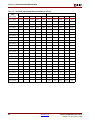
Date
Version
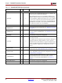
08/17/07
(cont’d)
4.0
(cont’d)
Revision
•
•
•
•
•
•
•
•
•
•
Modified “10-Bit Alignment for 8B/10B Encoded Data.”
Expanded SONET alignment sequence figure into Figure 3-15 and Figure 3-16.
Removed support of RXSYNC functionality in “RXSLIDE.”
Modified Figure 3-18.
Modified last paragraph of “Clock Correction Sequences.”
Removed RXBLOCKSYNC64B66BUSE column, last two rows (64B/66B), and note
from Table 3-14.
Modified Figure 3-24.
Modified nominal frequency and period in text following Table 3-25.
Removed Clocking in Buffer Bypass Mode section from Chapter 3.
Removed Buffer Bypass Mode column from Table 3-26.
Chapter 4:
•
•
•
•
Modified attribute definitions in Table 4-1.
Removed description of TXUSRCLK from “Clock and Data Recovery.”
Corrected references to RXAFEEQ in Figure 4-8.
Removed description of MGT from “POWERDOWN.”
Chapter 5:
• Added description of CRC wakeup in “Latency and Timing.”
Chapter 6:
•
•
•
•
Modified Figure 6-1 and Figure 6-4.
Corrected equation references in “Determining Power Supply Budget.”
Added additional bullet item to “Powering Unused MGTs.”
Modified text in “Reference Clock” and Figure 6-7.
Chapter 7:
• Added “Reference Clock Period Restriction.”
• Rewrote description of TXENOOB and RXSIGDET in “Out-of-Band (OOB)
Signaling.”
• Deleted TXENOOB and RXSIGDET, and added RXSYNC to “MGT Ports that Cannot
Be Simulated.”
Chapter 8:
• Modified note 2 after Table 8-1.
• Changed port name to RXBLOCKSYNC64B66BUSE in Table 8-3, Table 8-11, and
Table 8-12.
• Added notes to say that 64B/66B encoding/decoding is not supported in Figure 8-1,
Figure 8-2, Figure 8-4 to Figure 8-11, Figure 8-13, Figure 8-14, Figure 8-16 to
Figure 8-21, Table 8-1 to Table 8-9, Table 8-13 to Table 8-17.
• Added item 5 to “Usage.”
Chapter 9:
• Expanded description in “Clock Traces.”
Chapter 10:
• Rewrote “Optimal Cable Length.”
Appendix A:
• Removed 64B/66B from and modified descriptions of TXOUTCLK1/2 and
RXRECCLK1/2 in Table A-1.
• Added notes to Figure A-1, Table A-6, and Table A-7.
UG076 (v4.1) November 2, 2008
www.xilinx.com
Virtex-4 RocketIO MGT User Guide
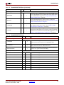
Date
Version
08/17/07
(cont’d)
4.0
(cont’d)
Revision
Appendix C:
• Modified Table C-2 to Table C-6, Table C-8 to Table C-11, Table C-13 to Table C-15,
Table C-17 to Table C-20, Table C-23, Table C-24, Table C-26, and Table C-27.
• Modified notes 1 and 3 after Table C-6 and Table C-25 and expanded note 4 after
Table C-6.
Appendix D:
• Expanded note in “Receiver Sample Phase Adjustment.”
Appendix E:
• Removed 64B/66B encoding scheme from Virtex-4 devices and added note 4 in
Table E-4.
• Modified Figure E-2.
• Modified text in “Loopback.”
• Removed section on TKERR[0] vs. TKERR[3].
• Removed section on clock correction and channel bonding sequences and
accompanying table.
• Removed discrete equalization row from Table E-10.
Modified references in Appendix F.
11/02/08
4.1
Added a new paragraph regarding 2.5V power and filtering to “Powering Unused
MGTs” in Chapter 6.
Virtex-4 RocketIO MGT User Guide
www.xilinx.com
UG076 (v4.1) November 2, 2008
Table of Contents
Preface: About This Guide
MGT Features . . . . . . . . . . . . . . . . . . . . . . . . . . . . . . . . . . . . . . . . . . . . . . . . . . . . . . . . . . . . . . .
User Guide Organization . . . . . . . . . . . . . . . . . . . . . . . . . . . . . . . . . . . . . . . . . . . . . . . . . . . .
Related Information . . . . . . . . . . . . . . . . . . . . . . . . . . . . . . . . . . . . . . . . . . . . . . . . . . . . . . . . .
Additional Resources . . . . . . . . . . . . . . . . . . . . . . . . . . . . . . . . . . . . . . . . . . . . . . . . . . . . . . .
User Guide Conventions . . . . . . . . . . . . . . . . . . . . . . . . . . . . . . . . . . . . . . . . . . . . . . . . . . . .
Logical / Mathematical Operators . . . . . . . . . . . . . . . . . . . . . . . . . . . . . . . . . . . . . . . . . .
Port and Attribute Names. . . . . . . . . . . . . . . . . . . . . . . . . . . . . . . . . . . . . . . . . . . . . . . . . .
Comma Definition . . . . . . . . . . . . . . . . . . . . . . . . . . . . . . . . . . . . . . . . . . . . . . . . . . . . . . . .
Jitter Definition . . . . . . . . . . . . . . . . . . . . . . . . . . . . . . . . . . . . . . . . . . . . . . . . . . . . . . . . . . .
Total Jitter (DJ + RJ) Definition . . . . . . . . . . . . . . . . . . . . . . . . . . . . . . . . . . . . . . . . . . . . .
MGT Definition . . . . . . . . . . . . . . . . . . . . . . . . . . . . . . . . . . . . . . . . . . . . . . . . . . . . . . . . . .
Typographical . . . . . . . . . . . . . . . . . . . . . . . . . . . . . . . . . . . . . . . . . . . . . . . . . . . . . . . . . . . .
27
28
29
29
29
29
30
30
30
30
30
31
Section I:
FPGA Level Design
Chapter 1: RocketIO Transceiver Overview
Basic Architecture and Capabilities . . . . . . . . . . . . . . . . . . . . . . . . . . . . . . . . . . . . . . . . . .
Configuring the RocketIO MGT . . . . . . . . . . . . . . . . . . . . . . . . . . . . . . . . . . . . . . . . . . . . .
Available Ports . . . . . . . . . . . . . . . . . . . . . . . . . . . . . . . . . . . . . . . . . . . . . . . . . . . . . . . . . . . . . .
Attributes . . . . . . . . . . . . . . . . . . . . . . . . . . . . . . . . . . . . . . . . . . . . . . . . . . . . . . . . . . . . . . . . . . .
Byte Mapping . . . . . . . . . . . . . . . . . . . . . . . . . . . . . . . . . . . . . . . . . . . . . . . . . . . . . . . . . . . . . . .
35
39
39
48
60
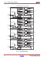
Chapter 2: Clocking, Timing, and Resets
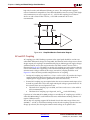
Clock Distribution . . . . . . . . . . . . . . . . . . . . . . . . . . . . . . . . . . . . . . . . . . . . . . . . . . . . . . . . . . 61
Column . . . . . . . . . . . . . . . . . . . . . . . . . . . . . . . . . . . . . . . . . . . . . . . . . . . . . . . . . . . . . . . . .
Tile . . . . . . . . . . . . . . . . . . . . . . . . . . . . . . . . . . . . . . . . . . . . . . . . . . . . . . . . . . . . . . . . . . . . .
MGT . . . . . . . . . . . . . . . . . . . . . . . . . . . . . . . . . . . . . . . . . . . . . . . . . . . . . . . . . . . . . . . . . . . .
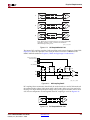
GT11CLK_MGT and Reference Clock Routing . . . . . . . . . . . . . . . . . . . . . . . . . . . . . . . .
MGT Clock Ports and Attributes . . . . . . . . . . . . . . . . . . . . . . . . . . . . . . . . . . . . . . . . . . . .
Common Reference Clock Use Models . . . . . . . . . . . . . . . . . . . . . . . . . . . . . . . . . . . . . .
High-Speed Dedicated MGT Clocks . . . . . . . . . . . . . . . . . . . . . . . . . . . . . . . . . . . . . . . .
Fabric Clocks . . . . . . . . . . . . . . . . . . . . . . . . . . . . . . . . . . . . . . . . . . . . . . . . . . . . . . . . . .
PMA Transmit Clocks . . . . . . . . . . . . . . . . . . . . . . . . . . . . . . . . . . . . . . . . . . . . . . . . . . . . .
PMA Receive Clocks . . . . . . . . . . . . . . . . . . . . . . . . . . . . . . . . . . . . . . . . . . . . . . . . . . . . . .
RX and TX PLL Voltage-Controlled Oscillator (VCO) Operating Frequency . . . . . .
61
61
61
63
64
66
66
67
68
70
72
PMA/PCS Clocking Domains and Data Paths . . . . . . . . . . . . . . . . . . . . . . . . . . . . . . . . 74
PMA Configurations . . . . . . . . . . . . . . . . . . . . . . . . . . . . . . . . . . . . . . . . . . . . . . . . . . . . . . 75
Common MGT Clocking Use Cases . . . . . . . . . . . . . . . . . . . . . . . . . . . . . . . . . . . . . . . . . 76
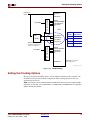
Setting the Clocking Options . . . . . . . . . . . . . . . . . . . . . . . . . . . . . . . . . . . . . . . . . . . . . . . . 77
Virtex-4 RocketIO MGT User Guide
UG076 (v4.1) November 2, 2008
www.xilinx.com
7
R
Special Clocking Considerations . . . . . . . . . . . . . . . . . . . . . . . . . . . . . . . . . . . . . . . . . . . . 82
RXCLKSTABLE and TXCLKSTABLE . . . . . . . . . . . . . . . . . . . . . . . . . . . . . . . . . . . . . . . . 82
Resets . . . . . . . . . . . . . . . . . . . . . . . . . . . . . . . . . . . . . . . . . . . . . . . . . . . . . . . . . . . . . . . . . . . . . . . 83
TXPMARESET . . . . . . . . . . . . . . . . . . . . . . . . . . . . . . . . . . . . . . . . . . . . . . . . . . . . . . . . . . . 83
RXPMARESET . . . . . . . . . . . . . . . . . . . . . . . . . . . . . . . . . . . . . . . . . . . . . . . . . . . . . . . . . . . 83
TXRESET . . . . . . . . . . . . . . . . . . . . . . . . . . . . . . . . . . . . . . . . . . . . . . . . . . . . . . . . . . . . . . . . 84
RXRESET . . . . . . . . . . . . . . . . . . . . . . . . . . . . . . . . . . . . . . . . . . . . . . . . . . . . . . . . . . . . . . . . 84
CRC Reset . . . . . . . . . . . . . . . . . . . . . . . . . . . . . . . . . . . . . . . . . . . . . . . . . . . . . . . . . . . . . . . 85
Resetting the Transceiver . . . . . . . . . . . . . . . . . . . . . . . . . . . . . . . . . . . . . . . . . . . . . . . . . . 85
Transmit Reset Sequence: TX Buffer Used . . . . . . . . . . . . . . . . . . . . . . . . . . . . . . . . . . . 85
Transmit Reset Sequence: TX Buffer Bypassed . . . . . . . . . . . . . . . . . . . . . . . . . . . . . . . . 88
Receive Reset Sequence: RX Buffer Used . . . . . . . . . . . . . . . . . . . . . . . . . . . . . . . . . . . . 93
Receive Reset Sequence: RX Buffer Bypassed . . . . . . . . . . . . . . . . . . . . . . . . . . . . . . . . . 96
Reset Considerations . . . . . . . . . . . . . . . . . . . . . . . . . . . . . . . . . . . . . . . . . . . . . . . . . . . 99
RX Reset Sequence Background . . . . . . . . . . . . . . . . . . . . . . . . . . . . . . . . . . . . . . . . . . 100
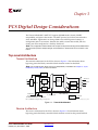
Chapter 3: PCS Digital Design Considerations
Top-Level Architecture . . . . . . . . . . . . . . . . . . . . . . . . . . . . . . . . . . . . . . . . . . . . . . . . . . . . . 101
Transmit Architecture . . . . . . . . . . . . . . . . . . . . . . . . . . . . . . . . . . . . . . . . . . . . . . . . . . . . 101
Receive Architecture . . . . . . . . . . . . . . . . . . . . . . . . . . . . . . . . . . . . . . . . . . . . . . . . . . . . . 101
Fabric Interface Synchronicity . . . . . . . . . . . . . . . . . . . . . . . . . . . . . . . . . . . . . . . . . . . . . . 102
RX Buffer . . . . . . . . . . . . . . . . . . . . . . . . . . . . . . . . . . . . . . . . . . . . . . . . . . . . . . . . . . . . . . . . . . 102
Bus Interface . . . . . . . . . . . . . . . . . . . . . . . . . . . . . . . . . . . . . . . . . . . . . . . . . . . . . . . . . . . . . . . 103
External Bus Width Configuration (Fabric Interface) . . . . . . . . . . . . . . . . . . . . . . . . . .
Internal Bus Width Configuration . . . . . . . . . . . . . . . . . . . . . . . . . . . . . . . . . . . . . . . . . .
Fabric Interface Functionality. . . . . . . . . . . . . . . . . . . . . . . . . . . . . . . . . . . . . . . . . . . . . .
PCS Bypass Byte Mapping . . . . . . . . . . . . . . . . . . . . . . . . . . . . . . . . . . . . . . . . . . . . . . . .
103
104
105
107
8B/10B Encoding/Decoding . . . . . . . . . . . . . . . . . . . . . . . . . . . . . . . . . . . . . . . . . . . . . . . . . 108
Encoder . . . . . . . . . . . . . . . . . . . . . . . . . . . . . . . . . . . . . . . . . . . . . . . . . . . . . . . . . . . . . . . .
TXCHARDISPVAL and TXCHARDISPMODE. . . . . . . . . . . . . . . . . . . . . . . . . . . . . . .
TXCHARISK . . . . . . . . . . . . . . . . . . . . . . . . . . . . . . . . . . . . . . . . . . . . . . . . . . . . . . . . .
TXRUNDISP . . . . . . . . . . . . . . . . . . . . . . . . . . . . . . . . . . . . . . . . . . . . . . . . . . . . . . . . .
TXKERR . . . . . . . . . . . . . . . . . . . . . . . . . . . . . . . . . . . . . . . . . . . . . . . . . . . . . . . . . . . .
Decoder . . . . . . . . . . . . . . . . . . . . . . . . . . . . . . . . . . . . . . . . . . . . . . . . . . . . . . . . . . . . . . . .
RXCHARISK and RXRUNDISP . . . . . . . . . . . . . . . . . . . . . . . . . . . . . . . . . . . . . . . . . .
RXDISPERR . . . . . . . . . . . . . . . . . . . . . . . . . . . . . . . . . . . . . . . . . . . . . . . . . . . . . . . . .
RXNOTINTABLE . . . . . . . . . . . . . . . . . . . . . . . . . . . . . . . . . . . . . . . . . . . . . . . . . . . . .
RXCHARISCOMMA . . . . . . . . . . . . . . . . . . . . . . . . . . . . . . . . . . . . . . . . . . . . . . . . . .
Non-Standard Running Disparity Example. . . . . . . . . . . . . . . . . . . . . . . . . . . . . . . . . .
Transmitting Vitesse Channel Bonding Sequence . . . . . . . . . . . . . . . . . . . . . . . . . . . .
Receiving Vitesse Channel Bonding Sequence . . . . . . . . . . . . . . . . . . . . . . . . . . . . . . .
109
110
111
111
111
112
113
113
114
114
115
115
115
Symbol Alignment and Detection (Comma Detection) . . . . . . . . . . . . . . . . . . . . . . 116
Summary . . . . . . . . . . . . . . . . . . . . . . . . . . . . . . . . . . . . . . . . . . . . . . . . . . . . . . . . . . . . . . .
Bypassing . . . . . . . . . . . . . . . . . . . . . . . . . . . . . . . . . . . . . . . . . . . . . . . . . . . . . . . . . . . . . .
8-Bit / 10-Bit Alignment . . . . . . . . . . . . . . . . . . . . . . . . . . . . . . . . . . . . . . . . . . . . . . . . . .
10-Bit Alignment for 8B/10B Encoded Data . . . . . . . . . . . . . . . . . . . . . . . . . . . . . . . . .
Determining Barrel Shifter Position . . . . . . . . . . . . . . . . . . . . . . . . . . . . . . . . . . . . . . .
SONET Alignment . . . . . . . . . . . . . . . . . . . . . . . . . . . . . . . . . . . . . . . . . . . . . . . . . . . . . . .
Alignment Status . . . . . . . . . . . . . . . . . . . . . . . . . . . . . . . . . . . . . . . . . . . . . . . . . . . . .
Byte Alignment . . . . . . . . . . . . . . . . . . . . . . . . . . . . . . . . . . . . . . . . . . . . . . . . . . . . . . . . . .
ALIGN_COMMA_WORD . . . . . . . . . . . . . . . . . . . . . . . . . . . . . . . . . . . . . . . . . . . . . .
8
www.xilinx.com
116
116
117
117
118
119
122
122
122
Virtex-4 RocketIO MGT User Guide
UG076 (v4.1) November 2, 2008
R
RXSLIDE . . . . . . . . . . . . . . . . . . . . . . . . . . . . . . . . . . . . . . . . . . . . . . . . . . . . . . . . . . . . . . . 123
Clock Correction . . . . . . . . . . . . . . . . . . . . . . . . . . . . . . . . . . . . . . . . . . . . . . . . . . . . . . . . . . . 123
Append/Remove Idle Clock Correction . . . . . . . . . . . . . . . . . . . . . . . . . . . . . . . . . . . .
Clock Correction Sequences . . . . . . . . . . . . . . . . . . . . . . . . . . . . . . . . . . . . . . . . . . . . . . .
CLK_COR_SEQ_1_MASK, CLK_COR_SEQ_2_MASK,
CLK_COR_SEQ_LEN Attributes . . . . . . . . . . . . . . . . . . . . . . . . . . . . . . . . . . . . . . . .
Determining Correct CLK_COR_MIN_LAT and CLK_COR_MAX_LAT . . . . . . . .
123
124
125
126
Channel Bonding . . . . . . . . . . . . . . . . . . . . . . . . . . . . . . . . . . . . . . . . . . . . . . . . . . . . . . . . . . 127
Details . . . . . . . . . . . . . . . . . . . . . . . . . . . . . . . . . . . . . . . . . . . . . . . . . . . . . . . . . . . . . . . . .
CCCB_ARBITRATOR_DISABLE = TRUE, CLOCK_CORRECTION_USE = FALSE . .
CCCB_ARBITRATOR_DISABLE = FALSE, CLOCK_CORRECTION_USE = TRUE . .
CCCB_ARBITRATOR_DISABLE Attribute . . . . . . . . . . . . . . . . . . . . . . . . . . . . . . . . .
127
127
127
129
CHAN_BOND_SEQ_1_MASK, CHAN_BOND_SEQ_2_MASK,
CHAN_BOND_SEQ_LEN, CHAN_BOND_SEQ_*_* Attributes . . . . . . . . . . . . . . . 130
Disable Channel Bonding . . . . . . . . . . . . . . . . . . . . . . . . . . . . . . . . . . . . . . . . . . . . . . . 130
Setting CHAN_BOND_LIMIT . . . . . . . . . . . . . . . . . . . . . . . . . . . . . . . . . . . . . . . . . . . 130
Implementation Guidelines . . . . . . . . . . . . . . . . . . . . . . . . . . . . . . . . . . . . . . . . . . . . . . . 130
RX Fabric Interface and Channel Bonding . . . . . . . . . . . . . . . . . . . . . . . . . . . . . . . . . . . 132
Status and Event Bus . . . . . . . . . . . . . . . . . . . . . . . . . . . . . . . . . . . . . . . . . . . . . . . . . . . . . . . 132
Status Indication . . . . . . . . . . . . . . . . . . . . . . . . . . . . . . . . . . . . . . . . . . . . . . . . . . . . . . . . .
Event Indication . . . . . . . . . . . . . . . . . . . . . . . . . . . . . . . . . . . . . . . . . . . . . . . . . . . . . . . . .
RXBUFERR . . . . . . . . . . . . . . . . . . . . . . . . . . . . . . . . . . . . . . . . . . . . . . . . . . . . . . . . . . . . .
TXBUFERR . . . . . . . . . . . . . . . . . . . . . . . . . . . . . . . . . . . . . . . . . . . . . . . . . . . . . . . . . . . . .
132
133
133
133
LOOPBACK . . . . . . . . . . . . . . . . . . . . . . . . . . . . . . . . . . . . . . . . . . . . . . . . . . . . . . . . . . . . . . . 133
Digital Receiver . . . . . . . . . . . . . . . . . . . . . . . . . . . . . . . . . . . . . . . . . . . . . . . . . . . . . . . . . . . . 134
Clocking in Buffered Mode . . . . . . . . . . . . . . . . . . . . . . . . . . . . . . . . . . . . . . . . . . . . . . . 136
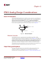
Chapter 4: PMA Analog Design Considerations
Serial I/O Description . . . . . . . . . . . . . . . . . . . . . . . . . . . . . . . . . . . . . . . . . . . . . . . . . . . . . . 139
Differential Transmitter . . . . . . . . . . . . . . . . . . . . . . . . . . . . . . . . . . . . . . . . . . . . . . . . . . 139
Output Swing and Emphasis . . . . . . . . . . . . . . . . . . . . . . . . . . . . . . . . . . . . . . . . . . . . . . . 139
Emphasis . . . . . . . . . . . . . . . . . . . . . . . . . . . . . . . . . . . . . . . . . . . . . . . . . . . . . . . . . . . . . . . 140
Differential Receiver . . . . . . . . . . . . . . . . . . . . . . . . . . . . . . . . . . . . . . . . . . . . . . . . . . . . . . . 146
Clock and Data Recovery . . . . . . . . . . . . . . . . . . . . . . . . . . . . . . . . . . . . . . . . . . . . . . . . . 146
Receiver Lock Control . . . . . . . . . . . . . . . . . . . . . . . . . . . . . . . . . . . . . . . . . . . . . . . . . . . . 147
Receive Equalization . . . . . . . . . . . . . . . . . . . . . . . . . . . . . . . . . . . . . . . . . . . . . . . . . . . . . 147
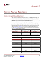
Special Analog Functions . . . . . . . . . . . . . . . . . . . . . . . . . . . . . . . . . . . . . . . . . . . . . . . . . . 149
Out-of-Band (OOB) Signals . . . . . . . . . . . . . . . . . . . . . . . . . . . . . . . . . . . . . . . . . . . . . . .
Calibration for the PLLs . . . . . . . . . . . . . . . . . . . . . . . . . . . . . . . . . . . . . . . . . . . . . . . . . .
POWERDOWN . . . . . . . . . . . . . . . . . . . . . . . . . . . . . . . . . . . . . . . . . . . . . . . . . . . . . . . . .
RXDCCOUPLE . . . . . . . . . . . . . . . . . . . . . . . . . . . . . . . . . . . . . . . . . . . . . . . . . . . . . . . . . .
RXPD . . . . . . . . . . . . . . . . . . . . . . . . . . . . . . . . . . . . . . . . . . . . . . . . . . . . . . . . . . . . . . . . . .
TXPD . . . . . . . . . . . . . . . . . . . . . . . . . . . . . . . . . . . . . . . . . . . . . . . . . . . . . . . . . . . . . . . . . .
149
149
151
152
152
152
Chapter 5: Cyclic Redundancy Check (CRC)
Functionality . . . . . . . . . . . . . . . . . . . . . . . . . . . . . . . . . . . . . . . . . . . . . . . . . . . . . . . . . . . . . . . 155
Handling End-of-Packet Residue . . . . . . . . . . . . . . . . . . . . . . . . . . . . . . . . . . . . . . . . . . . 157
Latency and Timing . . . . . . . . . . . . . . . . . . . . . . . . . . . . . . . . . . . . . . . . . . . . . . . . . . . . . . . . 157
64-Bit Example . . . . . . . . . . . . . . . . . . . . . . . . . . . . . . . . . . . . . . . . . . . . . . . . . . . . . . . . . . 158
Virtex-4 RocketIO MGT User Guide
UG076 (v4.1) November 2, 2008
www.xilinx.com
9
R
32-Bit Example . . . . . . . . . . . . . . . . . . . . . . . . . . . . . . . . . . . . . . . . . . . . . . . . . . . . . . . . . . 159
16-Bit Transmission, Hold CRC, and Residue of 8-Bit Example . . . . . . . . . . . . . . . . . 160
Implementation . . . . . . . . . . . . . . . . . . . . . . . . . . . . . . . . . . . . . . . . . . . . . . . . . . . . . . . . . . . . 161
Chapter 6: Analog and Board Design Considerations
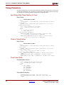
Physical Requirements . . . . . . . . . . . . . . . . . . . . . . . . . . . . . . . . . . . . . . . . . . . . . . . . . . . . . 163
Power Conditioning . . . . . . . . . . . . . . . . . . . . . . . . . . . . . . . . . . . . . . . . . . . . . . . . . . . . .
Power Supply Requirements . . . . . . . . . . . . . . . . . . . . . . . . . . . . . . . . . . . . . . . . . . . . . .
Determining Power Supply Budget . . . . . . . . . . . . . . . . . . . . . . . . . . . . . . . . . . . . . . .
Voltage Regulation . . . . . . . . . . . . . . . . . . . . . . . . . . . . . . . . . . . . . . . . . . . . . . . . . . . .
Powering Unused MGTs . . . . . . . . . . . . . . . . . . . . . . . . . . . . . . . . . . . . . . . . . . . . . . . . .
Reference Clock . . . . . . . . . . . . . . . . . . . . . . . . . . . . . . . . . . . . . . . . . . . . . . . . . . . . . . . . .
Termination . . . . . . . . . . . . . . . . . . . . . . . . . . . . . . . . . . . . . . . . . . . . . . . . . . . . . . . . . . . . .
AC and DC Coupling . . . . . . . . . . . . . . . . . . . . . . . . . . . . . . . . . . . . . . . . . . . . . . . . . . . .
SelectIO-to-MGT Crosstalk . . . . . . . . . . . . . . . . . . . . . . . . . . . . . . . . . . . . . . . . . . . . . . . .
163
165
165
166
168
170
171
172
174
High-Speed Serial Trace Design . . . . . . . . . . . . . . . . . . . . . . . . . . . . . . . . . . . . . . . . . . . . 176
Routing Serial Traces . . . . . . . . . . . . . . . . . . . . . . . . . . . . . . . . . . . . . . . . . . . . . . . . . . . . . 176
Differential Trace Design . . . . . . . . . . . . . . . . . . . . . . . . . . . . . . . . . . . . . . . . . . . . . . . . . 177
Chapter 7: Simulation and Implementation
Model Considerations . . . . . . . . . . . . . . . . . . . . . . . . . . . . . . . . . . . . . . . . . . . . . . . . . . . . . . 179
Simulation Models . . . . . . . . . . . . . . . . . . . . . . . . . . . . . . . . . . . . . . . . . . . . . . . . . . . . . . . . . 179
SmartModels . . . . . . . . . . . . . . . . . . . . . . . . . . . . . . . . . . . . . . . . . . . . . . . . . . . . . . . . . . . . 179
HSPICE . . . . . . . . . . . . . . . . . . . . . . . . . . . . . . . . . . . . . . . . . . . . . . . . . . . . . . . . . . . . . . . . 180
SmartModel Simulation Considerations . . . . . . . . . . . . . . . . . . . . . . . . . . . . . . . . . . . . 180
After Reset or Power-Up . . . . . . . . . . . . . . . . . . . . . . . . . . . . . . . . . . . . . . . . . . . . . . . . . .
Reference Clock Period Restriction . . . . . . . . . . . . . . . . . . . . . . . . . . . . . . . . . . . . . . . . .
RXP/RXN Period Restrictions . . . . . . . . . . . . . . . . . . . . . . . . . . . . . . . . . . . . . . . . . . . . .
Reset After Changing Clock Attributes . . . . . . . . . . . . . . . . . . . . . . . . . . . . . . . . . . . . .
Out-of-Band (OOB) Signaling . . . . . . . . . . . . . . . . . . . . . . . . . . . . . . . . . . . . . . . . . . . . .
1-Byte or 2-Byte Fabric Interface Width . . . . . . . . . . . . . . . . . . . . . . . . . . . . . . . . . . . . .
Loopback . . . . . . . . . . . . . . . . . . . . . . . . . . . . . . . . . . . . . . . . . . . . . . . . . . . . . . . . . . . . . . .
CRC . . . . . . . . . . . . . . . . . . . . . . . . . . . . . . . . . . . . . . . . . . . . . . . . . . . . . . . . . . . . . . . . . . .
Toggling GSR . . . . . . . . . . . . . . . . . . . . . . . . . . . . . . . . . . . . . . . . . . . . . . . . . . . . . . . . . . .
Simulating in Verilog . . . . . . . . . . . . . . . . . . . . . . . . . . . . . . . . . . . . . . . . . . . . . . . . . .
Simulating in VHDL . . . . . . . . . . . . . . . . . . . . . . . . . . . . . . . . . . . . . . . . . . . . . . . . . . .
Phase-Locked Loop . . . . . . . . . . . . . . . . . . . . . . . . . . . . . . . . . . . . . . . . . . . . . . . . . . . . . .
Frequency Calibration and Detector . . . . . . . . . . . . . . . . . . . . . . . . . . . . . . . . . . . . . . . .
SONET . . . . . . . . . . . . . . . . . . . . . . . . . . . . . . . . . . . . . . . . . . . . . . . . . . . . . . . . . . . . . . . . .
8B/10B Encoding/Decoding . . . . . . . . . . . . . . . . . . . . . . . . . . . . . . . . . . . . . . . . . . . . . .
MGT Ports that Cannot Be Simulated . . . . . . . . . . . . . . . . . . . . . . . . . . . . . . . . . . . . . . .
TXBUFFERR . . . . . . . . . . . . . . . . . . . . . . . . . . . . . . . . . . . . . . . . . . . . . . . . . . . . . . . . . . . .
180
180
180
180
181
181
181
181
181
182
182
184
184
184
184
185
185
Transceiver Location and Package Pin Relation . . . . . . . . . . . . . . . . . . . . . . . . . . . . . 186
MGT Package Pins . . . . . . . . . . . . . . . . . . . . . . . . . . . . . . . . . . . . . . . . . . . . . . . . . . . . . . . 186
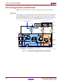
Chapter 8: Low-Latency Design
Introduction . . . . . . . . . . . . . . . . . . . . . . . . . . . . . . . . . . . . . . . . . . . . . . . . . . . . . . . . . . . . . . . 191
PCS Clocking Domains and Data Paths . . . . . . . . . . . . . . . . . . . . . . . . . . . . . . . . . . . . . 192
Receiver . . . . . . . . . . . . . . . . . . . . . . . . . . . . . . . . . . . . . . . . . . . . . . . . . . . . . . . . . . . . . . . . 192
10
www.xilinx.com
Virtex-4 RocketIO MGT User Guide
UG076 (v4.1) November 2, 2008
R
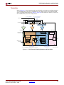
Transmitter . . . . . . . . . . . . . . . . . . . . . . . . . . . . . . . . . . . . . . . . . . . . . . . . . . . . . . . . . . . . . 193
PCS Data Path Latency . . . . . . . . . . . . . . . . . . . . . . . . . . . . . . . . . . . . . . . . . . . . . . . . . . . . . 194
Ports and Attributes . . . . . . . . . . . . . . . . . . . . . . . . . . . . . . . . . . . . . . . . . . . . . . . . . . . . . . . . 196
Receiver . . . . . . . . . . . . . . . . . . . . . . . . . . . . . . . . . . . . . . . . . . . . . . . . . . . . . . . . . . . . . . . . 196
Transmitter . . . . . . . . . . . . . . . . . . . . . . . . . . . . . . . . . . . . . . . . . . . . . . . . . . . . . . . . . . . . . 197
Synchronizing the PMA/PCS Clocks in Low-Latency Modes . . . . . . . . . . . . . . . . 197
Transmit Latency and Output Skew . . . . . . . . . . . . . . . . . . . . . . . . . . . . . . . . . . . . . . . . 198
TX Low-Latency Buffered Mode without Channel Deskew . . . . . . . . . . . . . . . . . . . .
Overview . . . . . . . . . . . . . . . . . . . . . . . . . . . . . . . . . . . . . . . . . . . . . . . . . . . . . . . . . . .
Clocking . . . . . . . . . . . . . . . . . . . . . . . . . . . . . . . . . . . . . . . . . . . . . . . . . . . . . . . . . . . .
Use Models . . . . . . . . . . . . . . . . . . . . . . . . . . . . . . . . . . . . . . . . . . . . . . . . . . . . . . . . . .
Skew . . . . . . . . . . . . . . . . . . . . . . . . . . . . . . . . . . . . . . . . . . . . . . . . . . . . . . . . . . . . . . .
Reset . . . . . . . . . . . . . . . . . . . . . . . . . . . . . . . . . . . . . . . . . . . . . . . . . . . . . . . . . . . . . . .
TX Low Latency Buffered Mode with Channel Deskew . . . . . . . . . . . . . . . . . . . . . . .
Overview . . . . . . . . . . . . . . . . . . . . . . . . . . . . . . . . . . . . . . . . . . . . . . . . . . . . . . . . . . .
Clocking . . . . . . . . . . . . . . . . . . . . . . . . . . . . . . . . . . . . . . . . . . . . . . . . . . . . . . . . . . . .
Use Models . . . . . . . . . . . . . . . . . . . . . . . . . . . . . . . . . . . . . . . . . . . . . . . . . . . . . . . . . .
Skew . . . . . . . . . . . . . . . . . . . . . . . . . . . . . . . . . . . . . . . . . . . . . . . . . . . . . . . . . . . . . . .
Reset . . . . . . . . . . . . . . . . . . . . . . . . . . . . . . . . . . . . . . . . . . . . . . . . . . . . . . . . . . . . . . .
TX Low Latency Buffer Bypass Mode . . . . . . . . . . . . . . . . . . . . . . . . . . . . . . . . . . . . . . .
Overview . . . . . . . . . . . . . . . . . . . . . . . . . . . . . . . . . . . . . . . . . . . . . . . . . . . . . . . . . . .
Clocking . . . . . . . . . . . . . . . . . . . . . . . . . . . . . . . . . . . . . . . . . . . . . . . . . . . . . . . . . . . .
Use Models . . . . . . . . . . . . . . . . . . . . . . . . . . . . . . . . . . . . . . . . . . . . . . . . . . . . . . . . . .
Skew . . . . . . . . . . . . . . . . . . . . . . . . . . . . . . . . . . . . . . . . . . . . . . . . . . . . . . . . . . . . . . .
Reset . . . . . . . . . . . . . . . . . . . . . . . . . . . . . . . . . . . . . . . . . . . . . . . . . . . . . . . . . . . . . . .
198
198
198
199
199
199
200
200
200
201
209
209
210
210
210
211
213
213
TXSYNC . . . . . . . . . . . . . . . . . . . . . . . . . . . . . . . . . . . . . . . . . . . . . . . . . . . . . . . . . . . . . . . . . . . 213
Overview . . . . . . . . . . . . . . . . . . . . . . . . . . . . . . . . . . . . . . . . . . . . . . . . . . . . . . . . . . . . . . . 213
Timing . . . . . . . . . . . . . . . . . . . . . . . . . . . . . . . . . . . . . . . . . . . . . . . . . . . . . . . . . . . . . . . . . 214
Usage . . . . . . . . . . . . . . . . . . . . . . . . . . . . . . . . . . . . . . . . . . . . . . . . . . . . . . . . . . . . . . . . . . 214
TX Channel Skew using TXSYNC . . . . . . . . . . . . . . . . . . . . . . . . . . . . . . . . . . . . . . . . . . 215
Worst-Case TX Skew Estimation . . . . . . . . . . . . . . . . . . . . . . . . . . . . . . . . . . . . . . . . . . .
Synchronization Clock = PCS TXCLK, TXPHASESEL = TRUE . . . . . . . . . . . . . . . . . .
Synchronization Clock = GREFCLK, TXPHASESEL = FALSE . . . . . . . . . . . . . . . . . . .
TX Skew Estimation Examples. . . . . . . . . . . . . . . . . . . . . . . . . . . . . . . . . . . . . . . . . . . . .
1.25 Gbit/s, Synchronization Clock = PCS TXCLK, TXPHASESEL = TRUE. . . . . . . . .
1.25 Gbit/s, Synchronization Clock = GREFCLK, TXPHASESEL = FALSE . . . . . . . . .
6.5 Gbit/s, Synchronization Clock = PCS TXCLK, TXPHASESEL = TRUE . . . . . . . . .
6.5 Gbit/s, Synchronization Clock = GREFCLK, TXPHASESEL = FALSE . . . . . . . . . .
215
215
216
217
217
217
217
217
RX Latency . . . . . . . . . . . . . . . . . . . . . . . . . . . . . . . . . . . . . . . . . . . . . . . . . . . . . . . . . . . . . . . . . 219
RX Low Latency Buffered Mode . . . . . . . . . . . . . . . . . . . . . . . . . . . . . . . . . . . . . . . . . . .
Overview . . . . . . . . . . . . . . . . . . . . . . . . . . . . . . . . . . . . . . . . . . . . . . . . . . . . . . . . . . .
Clocking . . . . . . . . . . . . . . . . . . . . . . . . . . . . . . . . . . . . . . . . . . . . . . . . . . . . . . . . . . . .
Use Models . . . . . . . . . . . . . . . . . . . . . . . . . . . . . . . . . . . . . . . . . . . . . . . . . . . . . . . . . .
Reset . . . . . . . . . . . . . . . . . . . . . . . . . . . . . . . . . . . . . . . . . . . . . . . . . . . . . . . . . . . . . . .
RX Low Latency Buffer Bypass Mode . . . . . . . . . . . . . . . . . . . . . . . . . . . . . . . . . . . . . .
Overview . . . . . . . . . . . . . . . . . . . . . . . . . . . . . . . . . . . . . . . . . . . . . . . . . . . . . . . . . . .
Clocking . . . . . . . . . . . . . . . . . . . . . . . . . . . . . . . . . . . . . . . . . . . . . . . . . . . . . . . . . . . .
Reset . . . . . . . . . . . . . . . . . . . . . . . . . . . . . . . . . . . . . . . . . . . . . . . . . . . . . . . . . . . . . . .
219
219
219
220
223
224
224
224
227
RXSYNC . . . . . . . . . . . . . . . . . . . . . . . . . . . . . . . . . . . . . . . . . . . . . . . . . . . . . . . . . . . . . . . . . . . 228
Overview . . . . . . . . . . . . . . . . . . . . . . . . . . . . . . . . . . . . . . . . . . . . . . . . . . . . . . . . . . . . . . . 228
Timing . . . . . . . . . . . . . . . . . . . . . . . . . . . . . . . . . . . . . . . . . . . . . . . . . . . . . . . . . . . . . . . . . 228
Usage . . . . . . . . . . . . . . . . . . . . . . . . . . . . . . . . . . . . . . . . . . . . . . . . . . . . . . . . . . . . . . . . . . 228
Virtex-4 RocketIO MGT User Guide
UG076 (v4.1) November 2, 2008
www.xilinx.com
11
R
Restrictions on Low Latency Buffer Bypass Modes . . . . . . . . . . . . . . . . . . . . . . . . . . 229
Example of a Reduced-Latency System . . . . . . . . . . . . . . . . . . . . . . . . . . . . . . . . . . . . . 230
XAUI . . . . . . . . . . . . . . . . . . . . . . . . . . . . . . . . . . . . . . . . . . . . . . . . . . . . . . . . . . . . . . . . . .
System Characteristics . . . . . . . . . . . . . . . . . . . . . . . . . . . . . . . . . . . . . . . . . . . . . . . . .
TX . . . . . . . . . . . . . . . . . . . . . . . . . . . . . . . . . . . . . . . . . . . . . . . . . . . . . . . . . . . . . . . . .
RX . . . . . . . . . . . . . . . . . . . . . . . . . . . . . . . . . . . . . . . . . . . . . . . . . . . . . . . . . . . . . . . . .
230
230
230
231
Section II:
Board Level Design
Chapter 9: Methodology Overview
Introduction . . . . . . . . . . . . . . . . . . . . . . . . . . . . . . . . . . . . . . . . . . . . . . . . . . . . . . . . . . . . . . . 235
Powering the RocketIO MGTs . . . . . . . . . . . . . . . . . . . . . . . . . . . . . . . . . . . . . . . . . . . . . 236
Regulators . . . . . . . . . . . . . . . . . . . . . . . . . . . . . . . . . . . . . . . . . . . . . . . . . . . . . . . . . . . . . . 236
Filtering . . . . . . . . . . . . . . . . . . . . . . . . . . . . . . . . . . . . . . . . . . . . . . . . . . . . . . . . . . . . . . . . 236
Reference Clock . . . . . . . . . . . . . . . . . . . . . . . . . . . . . . . . . . . . . . . . . . . . . . . . . . . . . . . . . . . . 236
Clock Sources . . . . . . . . . . . . . . . . . . . . . . . . . . . . . . . . . . . . . . . . . . . . . . . . . . . . . . . . . . . 236
Clock Traces . . . . . . . . . . . . . . . . . . . . . . . . . . . . . . . . . . . . . . . . . . . . . . . . . . . . . . . . . . . . 237
Coupling. . . . . . . . . . . . . . . . . . . . . . . . . . . . . . . . . . . . . . . . . . . . . . . . . . . . . . . . . . . . . . . . . . . 237
DC Coupling . . . . . . . . . . . . . . . . . . . . . . . . . . . . . . . . . . . . . . . . . . . . . . . . . . . . . . . . . . . . 237
AC Coupling . . . . . . . . . . . . . . . . . . . . . . . . . . . . . . . . . . . . . . . . . . . . . . . . . . . . . . . . . . . . 237
External Capacitor Value Selection . . . . . . . . . . . . . . . . . . . . . . . . . . . . . . . . . . . . . . . . . 237
Chapter 10: PCB Materials and Traces
How Fast is Fast? . . . . . . . . . . . . . . . . . . . . . . . . . . . . . . . . . . . . . . . . . . . . . . . . . . . . . . . . . . . 239
PCB Losses. . . . . . . . . . . . . . . . . . . . . . . . . . . . . . . . . . . . . . . . . . . . . . . . . . . . . . . . . . . . . . . . . 239
Relative Permittivity . . . . . . . . . . . . . . . . . . . . . . . . . . . . . . . . . . . . . . . . . . . . . . . . . . . . .
Loss Tangent . . . . . . . . . . . . . . . . . . . . . . . . . . . . . . . . . . . . . . . . . . . . . . . . . . . . . . . . . . . .
Skin Effect and Resistive Losses . . . . . . . . . . . . . . . . . . . . . . . . . . . . . . . . . . . . . . . . . . .
Choosing the Substrate Material . . . . . . . . . . . . . . . . . . . . . . . . . . . . . . . . . . . . . . . . . . .
240
240
240
240
Traces . . . . . . . . . . . . . . . . . . . . . . . . . . . . . . . . . . . . . . . . . . . . . . . . . . . . . . . . . . . . . . . . . . . . . . 241
Trace Geometry . . . . . . . . . . . . . . . . . . . . . . . . . . . . . . . . . . . . . . . . . . . . . . . . . . . . . . . . .
Trace Characteristic Impedance Design . . . . . . . . . . . . . . . . . . . . . . . . . . . . . . . . . . . . .
Trace Routing . . . . . . . . . . . . . . . . . . . . . . . . . . . . . . . . . . . . . . . . . . . . . . . . . . . . . . . . . . .
Plane Splits . . . . . . . . . . . . . . . . . . . . . . . . . . . . . . . . . . . . . . . . . . . . . . . . . . . . . . . . . . . . .
Simulating Lossy Transmission Lines. . . . . . . . . . . . . . . . . . . . . . . . . . . . . . . . . . . . . . .
241
241
243
243
243
Cable . . . . . . . . . . . . . . . . . . . . . . . . . . . . . . . . . . . . . . . . . . . . . . . . . . . . . . . . . . . . . . . . . . . . . . 244
Connectors . . . . . . . . . . . . . . . . . . . . . . . . . . . . . . . . . . . . . . . . . . . . . . . . . . . . . . . . . . . . . 244
Optimal Cable Length . . . . . . . . . . . . . . . . . . . . . . . . . . . . . . . . . . . . . . . . . . . . . . . . . . . . 244
Skew Between Conductors . . . . . . . . . . . . . . . . . . . . . . . . . . . . . . . . . . . . . . . . . . . . . . . . 244
Chapter 11: Design of Transitions
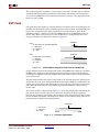
Excess Capacitance and Inductance . . . . . . . . . . . . . . . . . . . . . . . . . . . . . . . . . . . . . . . . .
Time Domain Reflectometry (TDR) . . . . . . . . . . . . . . . . . . . . . . . . . . . . . . . . . . . . . . . .
SMT Pads . . . . . . . . . . . . . . . . . . . . . . . . . . . . . . . . . . . . . . . . . . . . . . . . . . . . . . . . . . . . . . . . . .
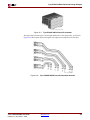
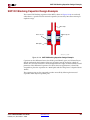
Differential Vias . . . . . . . . . . . . . . . . . . . . . . . . . . . . . . . . . . . . . . . . . . . . . . . . . . . . . . . . . . .
12
www.xilinx.com
245
245
247
250
Virtex-4 RocketIO MGT User Guide
UG076 (v4.1) November 2, 2008
R
Microstrip/Stripline Bends . . . . . . . . . . . . . . . . . . . . . . . . . . . . . . . . . . . . . . . . . . . . . . . . . 252
BGA Packages . . . . . . . . . . . . . . . . . . . . . . . . . . . . . . . . . . . . . . . . . . . . . . . . . . . . . . . . . . . . . 255
SMA Connectors . . . . . . . . . . . . . . . . . . . . . . . . . . . . . . . . . . . . . . . . . . . . . . . . . . . . . . . . . . . 255
Chapter 12: Guidelines and Examples
Summary of Guidelines . . . . . . . . . . . . . . . . . . . . . . . . . . . . . . . . . . . . . . . . . . . . . . . . . . . .
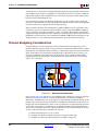
Channel Budgeting Considerations . . . . . . . . . . . . . . . . . . . . . . . . . . . . . . . . . . . . . . . . .
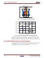
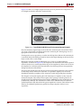
BGA Escape Example . . . . . . . . . . . . . . . . . . . . . . . . . . . . . . . . . . . . . . . . . . . . . . . . . . . . . .
SMT XENPAK70 Connector Design Example . . . . . . . . . . . . . . . . . . . . . . . . . . . . . .
SMT XFP Connector Design Example . . . . . . . . . . . . . . . . . . . . . . . . . . . . . . . . . . . . . .
Tyco Z-PACK HM-Zd Connector Design Example . . . . . . . . . . . . . . . . . . . . . . . . . .
SMT DC Blocking Capacitor Design Example . . . . . . . . . . . . . . . . . . . . . . . . . . . . . .
257
258
261
262
263
264
267
Section III:
Appendixes
Appendix A: RocketIO Transceiver Timing Model
Timing Parameters . . . . . . . . . . . . . . . . . . . . . . . . . . . . . . . . . . . . . . . . . . . . . . . . . . . . . . . . . 274
Input Setup/Hold Times Relative to Clock . . . . . . . . . . . . . . . . . . . . . . . . . . . . . . . . . . 274
Clock to Output Delays . . . . . . . . . . . . . . . . . . . . . . . . . . . . . . . . . . . . . . . . . . . . . . . . . . . 274
Clock Pulse Width . . . . . . . . . . . . . . . . . . . . . . . . . . . . . . . . . . . . . . . . . . . . . . . . . . . . . . . 274
Timing Diagram and Timing Parameter Tables . . . . . . . . . . . . . . . . . . . . . . . . . . . . . 275
Appendix B: 8B/10B Valid Characters
Valid Data and Control Characters . . . . . . . . . . . . . . . . . . . . . . . . . . . . . . . . . . . . . . . . . 283
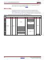
Appendix C: Dynamic Reconfiguration Port
Interface Description . . . . . . . . . . . . . . . . . . . . . . . . . . . . . . . . . . . . . . . . . . . . . . . . . . . . . . . 293
Memory Map . . . . . . . . . . . . . . . . . . . . . . . . . . . . . . . . . . . . . . . . . . . . . . . . . . . . . . . . . . . . . . 294
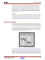
Appendix D: Special Analog Functions
Receiver Sample Phase Adjustment . . . . . . . . . . . . . . . . . . . . . . . . . . . . . . . . . . . . . . . . 321
Appendix E: Virtex-II Pro/Virtex-II Pro X to Virtex-4 RocketIO
Transceiver Design Migration
Introduction . . . . . . . . . . . . . . . . . . . . . . . . . . . . . . . . . . . . . . . . . . . . . . . . . . . . . . . . . . . . . . . 325
Primary Differences . . . . . . . . . . . . . . . . . . . . . . . . . . . . . . . . . . . . . . . . . . . . . . . . . . . . . . . . 325
MGTs per Device . . . . . . . . . . . . . . . . . . . . . . . . . . . . . . . . . . . . . . . . . . . . . . . . . . . . . . . .
Clocking . . . . . . . . . . . . . . . . . . . . . . . . . . . . . . . . . . . . . . . . . . . . . . . . . . . . . . . . . . . . . . . .
Serial Rate Support . . . . . . . . . . . . . . . . . . . . . . . . . . . . . . . . . . . . . . . . . . . . . . . . . . . . . .
Encoding Support and Clock Multipliers . . . . . . . . . . . . . . . . . . . . . . . . . . . . . . . . . . . .
Flexibility . . . . . . . . . . . . . . . . . . . . . . . . . . . . . . . . . . . . . . . . . . . . . . . . . . . . . . . . . . . . . . .
Board Guidelines . . . . . . . . . . . . . . . . . . . . . . . . . . . . . . . . . . . . . . . . . . . . . . . . . . . . . . . .
Virtex-4 RocketIO MGT User Guide
UG076 (v4.1) November 2, 2008
www.xilinx.com
325
326
327
327
327
328
13
R
Power Supply Filtering . . . . . . . . . . . . . . . . . . . . . . . . . . . . . . . . . . . . . . . . . . . . . . . . . 328
Other Minor Differences . . . . . . . . . . . . . . . . . . . . . . . . . . . . . . . . . . . . . . . . . . . . . . . . . . . 329
Termination . . . . . . . . . . . . . . . . . . . . . . . . . . . . . . . . . . . . . . . . . . . . . . . . . . . . . . . . . . . . .
CRC . . . . . . . . . . . . . . . . . . . . . . . . . . . . . . . . . . . . . . . . . . . . . . . . . . . . . . . . . . . . . . . . . . .
Loopback . . . . . . . . . . . . . . . . . . . . . . . . . . . . . . . . . . . . . . . . . . . . . . . . . . . . . . . . . . . . . . .
Serialization . . . . . . . . . . . . . . . . . . . . . . . . . . . . . . . . . . . . . . . . . . . . . . . . . . . . . . . . . . . .
RXSTATUS Bus . . . . . . . . . . . . . . . . . . . . . . . . . . . . . . . . . . . . . . . . . . . . . . . . . . . . . . . . .
329
330
330
330
331
Pre-emphasis, Differential Swing, and Equalization . . . . . . . . . . . . . . . . . . . . . . . . 331
Appendix F: References
14
www.xilinx.com
Virtex-4 RocketIO MGT User Guide
UG076 (v4.1) November 2, 2008
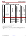
Schedule of Figures
Section I:
FPGA Level Design
Chapter 1: RocketIO Transceiver Overview
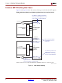
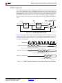
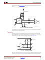
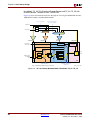
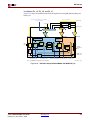
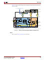
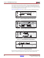
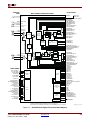
Figure 1-1: RocketIO Multi-Gigabit Transceiver Block Diagram. . . . . . . . . . . . . . . . . . . . 36
Chapter 2: Clocking, Timing, and Resets
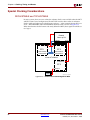
Figure 2-1: MGT Column Clocking . . . . . . . . . . . . . . . . . . . . . . . . . . . . . . . . . . . . . . . . . . . . . 62
Figure 2-2: High-Speed Dedicated Clocks (GT11CLK_MGT Instance) . . . . . . . . . . . . . . 66
Figure 2-3: REFCLK and GREFCLK Options for an MGT Tile . . . . . . . . . . . . . . . . . . . . . 67
Figure 2-4: MGT Transmit Clocking . . . . . . . . . . . . . . . . . . . . . . . . . . . . . . . . . . . . . . . . . . . . 68
Figure 2-5: MGT Receive Clocking. . . . . . . . . . . . . . . . . . . . . . . . . . . . . . . . . . . . . . . . . . . . . . 70
Figure 2-6: Transmitter and Receiver Line Rates . . . . . . . . . . . . . . . . . . . . . . . . . . . . . . . . . . 73
Figure 2-7: PCS Receive Clocking Domains and Datapaths . . . . . . . . . . . . . . . . . . . . . . . . 74
Figure 2-8: PCS Transmit Clocking Domains and Datapaths . . . . . . . . . . . . . . . . . . . . . . . 75
Figure 2-9: Low-Latency Clocking . . . . . . . . . . . . . . . . . . . . . . . . . . . . . . . . . . . . . . . . . . . . . . 76
Figure 2-10: DCM Clocking . . . . . . . . . . . . . . . . . . . . . . . . . . . . . . . . . . . . . . . . . . . . . . . . . . . . 77
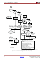
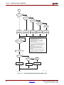
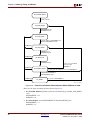
Figure 2-11: Receive Clocking Decision Flow (Page 1 of 2) . . . . . . . . . . . . . . . . . . . . . . . . . 78
Figure 2-11 (Cont’d): Receive Clocking Decision Flow (Page 2 of 2). . . . . . . . . . . . . . . . . . 79
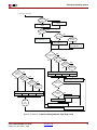
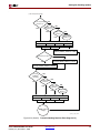
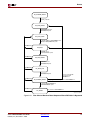
Figure 2-12: Transmit Clocking Decision Flow (Page 1 of 2). . . . . . . . . . . . . . . . . . . . . . . . 80
Figure 2-12 (Cont’d): Transmit Clocking Decision Flow (Page 2 of 2) . . . . . . . . . . . . . . . . 81
Figure 2-13: External PLL Locked Signal for MGT . . . . . . . . . . . . . . . . . . . . . . . . . . . . . . . . 82
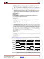
Figure 2-14: Flow Chart of TX Reset Sequence Where TX Buffer Is Used . . . . . . . . . . . . 86
Figure 2-15: Resetting the Transmitter Where TX Buffer Is Used . . . . . . . . . . . . . . . . . . . 87
Figure 2-16: Flow Chart of TX Reset Sequence Where TX Buffer Is Bypassed . . . . . . . . 88
Figure 2-17: Flow Chart of TX Reset Sequence Where TX Buffer Is Bypassed
and tx_align_err Is Not Used . . . . . . . . . . . . . . . . . . . . . . . . . . . . . . . . . . . . . . . . . . . . . . . . . 91
Figure 2-18: Resetting the Transmitter Where TX Buffer Is Bypassed . . . . . . . . . . . . . . . 93
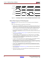
Figure 2-19: Flow Chart of Receiver Reset Sequence Where RX Buffer Is Used . . . . . . . 94
Figure 2-20: Resetting the Receiver in Digital CDR Mode Where RX Buffer Is Used . . 95
Figure 2-21: Resetting the Receiver in Analog CDR Mode Where RX Buffer Is Used . . 96
Figure 2-22: Flow Chart of Receiver Reset Sequence Where RX Buffer Is Bypassed . . . 97
Figure 2-23: Resetting the Receiver in Analog CDR Mode Where
RX Buffer Is Bypassed . . . . . . . . . . . . . . . . . . . . . . . . . . . . . . . . . . . . . . . . . . . . . . . . . . . . . . 99
Figure 2-24: TXRESET for 8-Byte External Data Interface Width . . . . . . . . . . . . . . . . . . . 100
Chapter 3: PCS Digital Design Considerations
Figure 3-1: Transmit Architecture . . . . . . . . . . . . . . . . . . . . . . . . . . . . . . . . . . . . . . . . . . . . . . 101
Virtex-4 RocketIO MGT User Guide
UG076 (v4.1) November 2, 2008
www.xilinx.com
15
R
Figure 3-2: Receive Architecture . . . . . . . . . . . . . . . . . . . . . . . . . . . . . . . . . . . . . . . . . . . . . . . 102
Figure 3-3: RX Ring Buffer Half-Full Upon Initialization . . . . . . . . . . . . . . . . . . . . . . . . . 102
Figure 3-4: RX Ring Buffer Overflow and Underflow . . . . . . . . . . . . . . . . . . . . . . . . . . . . 103
Figure 3-5: Fabric Interface Timing. . . . . . . . . . . . . . . . . . . . . . . . . . . . . . . . . . . . . . . . . . . . . 106
Figure 3-6: PCS Bypass Byte Mapping, 8-Byte External Fabric Width . . . . . . . . . . . . . . 107
Figure 3-7: PCS Bypass Byte Mapping, 4-Byte External Fabric Width . . . . . . . . . . . . . . 107
Figure 3-8: 8B/10B Parallel-to-Serial Conversion . . . . . . . . . . . . . . . . . . . . . . . . . . . . . . . . . 108
Figure 3-9: 4-Byte Serial Structure. . . . . . . . . . . . . . . . . . . . . . . . . . . . . . . . . . . . . . . . . . . . . . 108
Figure 3-10: 10-Bit TX Data Map with 8B/10B Bypassed . . . . . . . . . . . . . . . . . . . . . . . . . . 111
Figure 3-11: 10-Bit RX Data Map with 8B/10B Bypassed . . . . . . . . . . . . . . . . . . . . . . . . . . 112
Figure 3-12: 8B/10B Comma Detection Example . . . . . . . . . . . . . . . . . . . . . . . . . . . . . . . . . 117
Figure 3-13: 6-Bit Alignment Mux Position. . . . . . . . . . . . . . . . . . . . . . . . . . . . . . . . . . . . . . 118
Figure 3-14: SONET Alignment Data Flow . . . . . . . . . . . . . . . . . . . . . . . . . . . . . . . . . . . . . . 119
Figure 3-15: SONET Alignment Sequence (4-Byte External Data Interface Width) . . . 119
Figure 3-16: SONET Alignment Sequence (2-Byte External Data Interface Width) . . . 120
Figure 3-17: Comma Placement . . . . . . . . . . . . . . . . . . . . . . . . . . . . . . . . . . . . . . . . . . . . . . . . 122
Figure 3-18: RXSLIDE Timing Waveform . . . . . . . . . . . . . . . . . . . . . . . . . . . . . . . . . . . . . . . 123
Figure 3-19: Effects of CCCB_ARBITRATOR_DISABLE = TRUE. . . . . . . . . . . . . . . . . . 130
Figure 3-20: Daisy-Chained Transceiver CHBONDI/CHBONDO Buses . . . . . . . . . . . . 131
Figure 3-21: XC4VFX20/XC4VFX60 Device Implementation . . . . . . . . . . . . . . . . . . . . . . . 131
Figure 3-22: Loopback Modes . . . . . . . . . . . . . . . . . . . . . . . . . . . . . . . . . . . . . . . . . . . . . . . . . 134
Figure 3-23: Digital Receiver Example . . . . . . . . . . . . . . . . . . . . . . . . . . . . . . . . . . . . . . . . . . 135
Figure 3-24: PCS RXCLK Generation, Buffered Mode (Green) . . . . . . . . . . . . . . . . . . . . 136
Chapter 4: PMA Analog Design Considerations
Figure 4-1: Differential Amplifier. . . . . . . . . . . . . . . . . . . . . . . . . . . . . . . . . . . . . . . . . . . . . . 139
Figure 4-2: 3-Tap Pre-Emphasis . . . . . . . . . . . . . . . . . . . . . . . . . . . . . . . . . . . . . . . . . . . . . . . . 140
Figure 4-3: Effect of 3-Tap Pre-Emphasis on a Pulse Signal . . . . . . . . . . . . . . . . . . . . . . . 141
Figure 4-4: TX with Minimal Pre-Emphasis . . . . . . . . . . . . . . . . . . . . . . . . . . . . . . . . . . . . . 143
Figure 4-5: RX after 36 Inches FR4 and Minimal Pre-Emphasis . . . . . . . . . . . . . . . . . . . . 144
Figure 4-6: TX with Maximal Pre-Emphasis . . . . . . . . . . . . . . . . . . . . . . . . . . . . . . . . . . . . . 145
Figure 4-7: RX after 36 Inches FR4 and Maximal Pre-Emphasis . . . . . . . . . . . . . . . . . . . . 146
Figure 4-8: AC Response of Continuous-Time Linear Receiver Equalizer. . . . . . . . . . . 148
Figure 4-9: OOB Signal . . . . . . . . . . . . . . . . . . . . . . . . . . . . . . . . . . . . . . . . . . . . . . . . . . . . . . . 149
Chapter 5: Cyclic Redundancy Check (CRC)
Figure 5-1: 32-bit CRC Inputs and Outputs. . . . . . . . . . . . . . . . . . . . . . . . . . . . . . . . . . . . . . 153
Figure 5-2: 64-Bit to 32-Bit Core Interface . . . . . . . . . . . . . . . . . . . . . . . . . . . . . . . . . . . . . . . 156
Figure 5-3: Max Data Rate Example (64-Bit) . . . . . . . . . . . . . . . . . . . . . . . . . . . . . . . . . . . . . 158
Figure 5-4: Max Data Rate Example (32-Bit) . . . . . . . . . . . . . . . . . . . . . . . . . . . . . . . . . . . . . 159
Figure 5-5: 16-Bit Transmission, Hold CRC, and Residue of 8-Bit Example . . . . . . . . . 160
Figure 5-6: CRC Generation Diagram . . . . . . . . . . . . . . . . . . . . . . . . . . . . . . . . . . . . . . . . . . 161
16
www.xilinx.com
Virtex-4 RocketIO MGT User Guide
UG076 (v4.1) November 2, 2008
R
Chapter 6: Analog and Board Design Considerations
Figure 6-1: MGT Tile Power and Serial I/O Pins . . . . . . . . . . . . . . . . . . . . . . . . . . . . . . . . . 164
Figure 6-2: Internal Receiver AC Coupling with External DC Coupling between
Transmitter and Receiver Terminations . . . . . . . . . . . . . . . . . . . . . . . . . . . . . . . . . . . . . . 166
Figure 6-3: Power Supply Circuit . . . . . . . . . . . . . . . . . . . . . . . . . . . . . . . . . . . . . . . . . . . . . . 166
Figure 6-4: Power Filtering Network for One MGT Tile . . . . . . . . . . . . . . . . . . . . . . . . . . 167
Figure 6-5: Layout for Power Filtering Network . . . . . . . . . . . . . . . . . . . . . . . . . . . . . . . . . 168
Figure 6-6: Optimizing Filtering for an MGT Column. . . . . . . . . . . . . . . . . . . . . . . . . . . . 169
Figure 6-7: Reference Clock Oscillator Interface (Up to 400 MHz) . . . . . . . . . . . . . . . . . 170
Figure 6-8: Reference Clock VCSO . . . . . . . . . . . . . . . . . . . . . . . . . . . . . . . . . . . . . . . . . . . . . 171
Figure 6-9: Transmit Termination . . . . . . . . . . . . . . . . . . . . . . . . . . . . . . . . . . . . . . . . . . . . . . 171
Figure 6-10: Simplified Receive Termination Diagram . . . . . . . . . . . . . . . . . . . . . . . . . . . 172
Figure 6-11: AC-Coupled Serial Link . . . . . . . . . . . . . . . . . . . . . . . . . . . . . . . . . . . . . . . . . . . 173
Figure 6-12: AC Coupling Detail . . . . . . . . . . . . . . . . . . . . . . . . . . . . . . . . . . . . . . . . . . . . . . . 173
Figure 6-13: DC-Coupled Serial Link . . . . . . . . . . . . . . . . . . . . . . . . . . . . . . . . . . . . . . . . . . . 173
Figure 6-14: Single-Ended Trace Geometry. . . . . . . . . . . . . . . . . . . . . . . . . . . . . . . . . . . . . . 177
Figure 6-15: Obstacle Route Geometry. . . . . . . . . . . . . . . . . . . . . . . . . . . . . . . . . . . . . . . . . . 178
Figure 6-16: Microstrip Edge-Coupled Differential Pair . . . . . . . . . . . . . . . . . . . . . . . . . . 178
Figure 6-17: Stripline Edge-Coupled Differential Pair . . . . . . . . . . . . . . . . . . . . . . . . . . . . 178
Chapter 7: Simulation and Implementation
Chapter 8: Low-Latency Design
Figure 8-1: PCS Receive Clocking Domains and Data Paths. . . . . . . . . . . . . . . . . . . . . . . 192
Figure 8-2: PCS Transmit Clocking Domains and Data Paths . . . . . . . . . . . . . . . . . . . . . 193
Figure 8-3: Using GREFCLK as Synchronization Clock (Use Models TX_2A-H) . . . . . 200
Figure 8-4: TX Low Latency Buffered Mode: Use Models TX_1A, TX_2A . . . . . . . . . . . 202
Figure 8-5: TX Low Latency Buffered Mode: Use Models TX_1B, TX_2B. . . . . . . . . . . . 203
Figure 8-6: TX Low Latency Buffered Mode: Use Models TX_1C, TX_2C . . . . . . . . . . . 204
Figure 8-7: TX Low Latency Buffered Mode: Use Models TX_1D, TX_2D . . . . . . . . . . . 205
Figure 8-8: TX Low Latency Buffered Mode: Use Model TX_2E. . . . . . . . . . . . . . . . . . . . 206
Figure 8-9: TX Low Latency Buffered Mode: Use Model TX_2F. . . . . . . . . . . . . . . . . . . . 207
Figure 8-10: TX Low Latency Buffered Mode: Use Model TX_2G . . . . . . . . . . . . . . . . . . 208
Figure 8-11: TX Low Latency Buffered Mode: Use Model TX_2H . . . . . . . . . . . . . . . . . . 209
Figure 8-12: Using PCS TXCLK as Synchronization Clock (Use Models TX_3A-B). . . 210
Figure 8-13: TX Low Latency Buffer Bypass Mode: Use Model TX_3A . . . . . . . . . . . . . 212
Figure 8-14: TX Low Latency Buffer Bypass Mode: Use Model TX_3B . . . . . . . . . . . . . . 213
Figure 8-15: TXSYNC Timing . . . . . . . . . . . . . . . . . . . . . . . . . . . . . . . . . . . . . . . . . . . . . . . . . 214
Figure 8-16: RX Low Latency Buffered Mode: Use Model RX_1A . . . . . . . . . . . . . . . . . . 221
Figure 8-17: RX Low Latency Buffered Mode: Use Model RX_1B . . . . . . . . . . . . . . . . . . 222
Figure 8-18: RX Low Latency Buffered Mode: Use Model RX_1C . . . . . . . . . . . . . . . . . . 223
Figure 8-19: RX Low Latency Buffer Bypass Mode: Use Model RX_2A . . . . . . . . . . . . . 225
Figure 8-20: RX Low Latency Buffer Bypass Mode: Use Model RX_2B . . . . . . . . . . . . . 226
Virtex-4 RocketIO MGT User Guide
UG076 (v4.1) November 2, 2008
www.xilinx.com
17
R
Figure 8-21: RX Low Latency Buffer Bypass Mode: Use Model RX_2C . . . . . . . . . . . . . 227
Figure 8-22: RXSYNC Timing . . . . . . . . . . . . . . . . . . . . . . . . . . . . . . . . . . . . . . . . . . . . . . . . . 228
Section II:
Board Level Design
Chapter 9: Methodology Overview
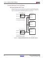
Figure 9-1: Two RocketIO MGTs Interconnected . . . . . . . . . . . . . . . . . . . . . . . . . . . . . . . . 235
Chapter 10: PCB Materials and Traces
Figure 10-1: Differential Edge-Coupled Centered Stripline . . . . . . . . . . . . . . . . . . . . . . . 242
Figure 10-2: Differential Edge-Coupled Offset Stripline . . . . . . . . . . . . . . . . . . . . . . . . . . 242
Figure 10-3: Centered Broadside-Coupled Stripline . . . . . . . . . . . . . . . . . . . . . . . . . . . . . . 242
Figure 10-4: Differential Microstrip . . . . . . . . . . . . . . . . . . . . . . . . . . . . . . . . . . . . . . . . . . . . 242
Chapter 11: Design of Transitions
Figure 11-1: TDR Signature of Shunt Capacitance . . . . . . . . . . . . . . . . . . . . . . . . . . . . . . . 246
Figure 11-2: TDR Signature of Series Inductance . . . . . . . . . . . . . . . . . . . . . . . . . . . . . . . . 246
Figure 11-3: Integration of Normalized TDR Area . . . . . . . . . . . . . . . . . . . . . . . . . . . . . . . 246
Figure 11-4: 2D Field Solver Analysis of 5 Mil Trace and 28 Mil Pad . . . . . . . . . . . . . . . 247
Figure 11-5: Transition Optimization . . . . . . . . . . . . . . . . . . . . . . . . . . . . . . . . . . . . . . . . . . . 247
Figure 11-6: Ansoft HFSS Model of Capacitor with a Pad Clear-Out . . . . . . . . . . . . . . . 248
Figure 11-7: Return Loss Comparison Between 0402 Pad Structures . . . . . . . . . . . . . . . . 248
Figure 11-8: Return Loss Comparison Between 0402 Pad Structures
on Log (Frequency) Scale . . . . . . . . . . . . . . . . . . . . . . . . . . . . . . . . . . . . . . . . . . . . . . . . . . . 249
Figure 11-9: TDR Results Comparing 0402 Pad Structures
with Excess Capacitance Reduced from 840 fF to 70 fF . . . . . . . . . . . . . . . . . . . . . . . . . 249
Figure 11-10: Differential Via Design Example . . . . . . . . . . . . . . . . . . . . . . . . . . . . . . . . . . 250
Figure 11-11: Differential GSSG Via in 16-layer PCB from Pins L11 and L6 . . . . . . . . . 251
Figure 11-12: Simulated Return Loss Comparing Differential and Common-Mode
Losses for L11 and L6 GSSG Vias . . . . . . . . . . . . . . . . . . . . . . . . . . . . . . . . . . . . . . . . . . . 251
Figure 11-13: Example Design for 90 Degree Bends in Traces . . . . . . . . . . . . . . . . . . . . . 252
Figure 11-14: Simulated TDR of 45 Degree Bends with Jog-Outs . . . . . . . . . . . . . . . . . . 253
Figure 11-15: Simulated Return Loss of 45 Degree Bends with Jog-Outs . . . . . . . . . . . . 253
Figure 11-16: Simulated Phase Response of 45 Degree Bends with Jog-Outs . . . . . . . . 254
Figure 11-17: 90° Mitered Turns without and with Jog-Outs. . . . . . . . . . . . . . . . . . . . . . . 254
Figure 11-18: Measured TDR of Differential Pair with Four Mitered 90° Turns,
with and without Jog-Outs . . . . . . . . . . . . . . . . . . . . . . . . . . . . . . . . . . . . . . . . . . . . . . . . . 255
Chapter 12: Guidelines and Examples
Figure 12-1: Differential Via Dimensions . . . . . . . . . . . . . . . . . . . . . . . . . . . . . . . . . . . . . . . 258
Figure 12-2: BGA Escape Design Example . . . . . . . . . . . . . . . . . . . . . . . . . . . . . . . . . . . . . . 261
18
www.xilinx.com
Virtex-4 RocketIO MGT User Guide
UG076 (v4.1) November 2, 2008
R
Figure 12-3: Via Structures for BGA Adjacent SIO . . . . . . . . . . . . . . . . . . . . . . . . . . . . . . . 262
Figure 12-4: XENPAK70 Connector Design Example . . . . . . . . . . . . . . . . . . . . . . . . . . . . . 263
Figure 12-5: SMT XFP Connector Design Example . . . . . . . . . . . . . . . . . . . . . . . . . . . . . . . 264
Figure 12-6: SMT XFP Connector Return Loss Simulation Results . . . . . . . . . . . . . . . . . 264
Figure 12-7: Tyco Z-PACK HM-Zd Press-Fit Connector. . . . . . . . . . . . . . . . . . . . . . . . . . . 265
Figure 12-8: Tyco Z-PACK HM-Zd Press-Fit Connector Internals . . . . . . . . . . . . . . . . . . 265
Figure 12-9: Tyco Z-PACK HM-Zd Press-Fit Connector Design Example . . . . . . . . . . . 266
Figure 12-10: SMT DC Blocking Capacitor Design Example . . . . . . . . . . . . . . . . . . . . . . 267
Section III:
Appendixes
Appendix A: RocketIO Transceiver Timing Model
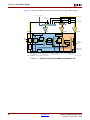
Figure A-1: RocketIO Multi-Gigabit Transceiver Block Diagram . . . . . . . . . . . . . . . . . . 273
Figure A-2: MGT Timing Relative to Clock Edge . . . . . . . . . . . . . . . . . . . . . . . . . . . . . . . . 275
Appendix B: 8B/10B Valid Characters
Appendix C: Dynamic Reconfiguration Port
Appendix D: Special Analog Functions
Appendix E: Virtex-II Pro/Virtex-II Pro X to Virtex-4 RocketIO
Transceiver Design Migration
Figure E-1: Reference Clock Selection for Each Device . . . . . . . . . . . . . . . . . . . . . . . . . . . 326
Figure E-2: Virtex-II, Virtex-II Pro, and Virtex-4 Power Supply Filtering . . . . . . . . . . . 329
Appendix F: References
Virtex-4 RocketIO MGT User Guide
UG076 (v4.1) November 2, 2008
www.xilinx.com
19
R
20
www.xilinx.com
Virtex-4 RocketIO MGT User Guide
UG076 (v4.1) November 2, 2008
Schedule of Tables
Section I:
FPGA Level Design
Chapter 1: RocketIO Transceiver Overview
Table 1-1: Number of MGT Cores per Device Type . . . . . . . . . . . . . . . . . . . . . . . . . . . . . . . 35
Table 1-2: Communications Standards Supported by the MGT . . . . . . . . . . . . . . . . . . . . . 35
Table 1-3: MGT Protocol Settings . . . . . . . . . . . . . . . . . . . . . . . . . . . . . . . . . . . . . . . . . . . . . . . 37
Table 1-4: RocketIO MGT CRC Ports . . . . . . . . . . . . . . . . . . . . . . . . . . . . . . . . . . . . . . . . . . . . 40
Table 1-5: RocketIO MGT PMA Ports . . . . . . . . . . . . . . . . . . . . . . . . . . . . . . . . . . . . . . . . . . . 41
Table 1-6: RocketIO MGT PCS Ports . . . . . . . . . . . . . . . . . . . . . . . . . . . . . . . . . . . . . . . . . . . . 43
Table 1-7: RocketIO MGT General Ports . . . . . . . . . . . . . . . . . . . . . . . . . . . . . . . . . . . . . . . . . 47
Table 1-8: RocketIO MGT Dynamic Reconfiguration Ports . . . . . . . . . . . . . . . . . . . . . . . . 47
Table 1-9: RocketIO MGT Communications Ports . . . . . . . . . . . . . . . . . . . . . . . . . . . . . . . . 47
Table 1-10: RocketIO MGT CRC Attributes . . . . . . . . . . . . . . . . . . . . . . . . . . . . . . . . . . . . . . 48
Table 1-11: RocketIO MGT PMA Attributes. . . . . . . . . . . . . . . . . . . . . . . . . . . . . . . . . . . . . . 50
Table 1-12: RocketIO MGT PCS Attributes. . . . . . . . . . . . . . . . . . . . . . . . . . . . . . . . . . . . . . . 54
Table 1-13: RocketIO MGT Digital Receiver Attributes. . . . . . . . . . . . . . . . . . . . . . . . . . . . 59
Table 1-14: MGT Tile Communication Attributes . . . . . . . . . . . . . . . . . . . . . . . . . . . . . . . . 60
Table 1-15: Control/Status Bus Association to Data Bus Byte Paths. . . . . . . . . . . . . . . . . . 60
Chapter 2: Clocking, Timing, and Resets
Table 2-1: MGTCLK Ports and Attributes . . . . . . . . . . . . . . . . . . . . . . . . . . . . . . . . . . . . . . . . 63
Table 2-2: MGT Clock Ports . . . . . . . . . . . . . . . . . . . . . . . . . . . . . . . . . . . . . . . . . . . . . . . . . . . . 64
Table 2-3: Clock Selection for Three PLLs in a Tile. . . . . . . . . . . . . . . . . . . . . . . . . . . . . . . . 65
Table 2-4: TX PMA Attribute Values(1) . . . . . . . . . . . . . . . . . . . . . . . . . . . . . . . . . . . . . . . . . . 69
Table 2-5: Supported Transmitter PLL Divider Combinations . . . . . . . . . . . . . . . . . . . . . . 69
Table 2-6: RX PMA Attribute Values(1) . . . . . . . . . . . . . . . . . . . . . . . . . . . . . . . . . . . . . . . . . . 71
Table 2-7: Supported Receiver PLL Divider Combinations . . . . . . . . . . . . . . . . . . . . . . . . . 72
Table 2-8: Supported VCO Operating Frequency Ranges . . . . . . . . . . . . . . . . . . . . . . . . . . 72
Table 2-9: MGT Reset Signals . . . . . . . . . . . . . . . . . . . . . . . . . . . . . . . . . . . . . . . . . . . . . . . . . . 83
Chapter 3: PCS Digital Design Considerations
Table 3-1: Selecting the External Configuration. . . . . . . . . . . . . . . . . . . . . . . . . . . . . . . . . . 104
Table 3-2: Selecting the Internal Configuration . . . . . . . . . . . . . . . . . . . . . . . . . . . . . . . . . . 104
Table 3-3: Fabric Interface Functionality . . . . . . . . . . . . . . . . . . . . . . . . . . . . . . . . . . . . . . . . 105
Table 3-4: 8B/10B Signal Definitions . . . . . . . . . . . . . . . . . . . . . . . . . . . . . . . . . . . . . . . . . . . 110
Table 3-5: Running Disparity Control . . . . . . . . . . . . . . . . . . . . . . . . . . . . . . . . . . . . . . . . . . 110
Table 3-6: 8B/10B Bypassed Signal Significance . . . . . . . . . . . . . . . . . . . . . . . . . . . . . . . . . 113
Virtex-4 RocketIO MGT User Guide
UG076 (v4.1) November 2, 2008
www.xilinx.com
21
R
Table 3-7: RXCHARISCOMMA Truth Table . . . . . . . . . . . . . . . . . . . . . . . . . . . . . . . . . . . . 114
Table 3-8: Deserializer Comma Detection Bypass . . . . . . . . . . . . . . . . . . . . . . . . . . . . . . . . 116
Table 3-9: 8B/10B Comma Symbol Configuration . . . . . . . . . . . . . . . . . . . . . . . . . . . . . . . . 118
Table 3-10: 8B/10B Decoder Byte-Mapped Status Flags . . . . . . . . . . . . . . . . . . . . . . . . . . . 118
Table 3-11: SONET Port Configuration . . . . . . . . . . . . . . . . . . . . . . . . . . . . . . . . . . . . . . . . . 120
Table 3-12: SONET Attribute Configuration . . . . . . . . . . . . . . . . . . . . . . . . . . . . . . . . . . . . 121
Table 3-13: ALIGN_COMMA_WORD Functionality . . . . . . . . . . . . . . . . . . . . . . . . . . . . . 122
Table 3-14: Definition of Clock Correction Sequence Bits 9-0. . . . . . . . . . . . . . . . . . . . . . 125
Table 3-15: Clock Correction Sequence/Data Correlation . . . . . . . . . . . . . . . . . . . . . . . . . 125
Table 3-16: Clock Correction Mask Example Settings (No Mask) . . . . . . . . . . . . . . . . . . 125
Table 3-17: Clock Correction Mask Example Settings (Mask Enabled). . . . . . . . . . . . . . 126
Table 3-18: Channel Bond Alignment Sequence . . . . . . . . . . . . . . . . . . . . . . . . . . . . . . . . . 127
Table 3-19: Maximum Time Required to Process Channel Bond Sequences . . . . . . . . . 128
Table 3-20: Channel Bonding and Clock Correction Character Spacing . . . . . . . . . . . . . 129
Table 3-21: Signal Values for a Pointer Difference Status . . . . . . . . . . . . . . . . . . . . . . . . . 132
Table 3-22: Signal Values for a Channel Bonding Skew . . . . . . . . . . . . . . . . . . . . . . . . . . 132
Table 3-23: Signal Values for Event Indication . . . . . . . . . . . . . . . . . . . . . . . . . . . . . . . . . . 133
Table 3-24: Loopback Modes . . . . . . . . . . . . . . . . . . . . . . . . . . . . . . . . . . . . . . . . . . . . . . . . . . 134
Table 3-25: Variation of Recovered Clock Period. . . . . . . . . . . . . . . . . . . . . . . . . . . . . . . . . 135
Table 3-26: Digital Receiver Attribute Settings (Line Rates ≤1.25 Gb/s) . . . . . . . . . . . . . 136
Chapter 4: PMA Analog Design Considerations
Table 4-1: Attributes Controlling Pre-Emphasis Characteristics. . . . . . . . . . . . . . . . . . . . 140
Table 4-2: TXDAT_TAP_DAC and TXPOST_TAP_DAC Settings . . . . . . . . . . . . . . . . . . 141
Table 4-3: RXDIGRX Definition . . . . . . . . . . . . . . . . . . . . . . . . . . . . . . . . . . . . . . . . . . . . . . . 147
Table 4-4: Transmit Calibration . . . . . . . . . . . . . . . . . . . . . . . . . . . . . . . . . . . . . . . . . . . . . . . . 149
Table 4-5: Receive Calibration . . . . . . . . . . . . . . . . . . . . . . . . . . . . . . . . . . . . . . . . . . . . . . . . . 150
Table 4-6: PLL/Data Frequency Divergence as a Function of Lock and Hysteresis. . . . 151
Table 4-7: RocketIO Transceiver Power Control Description . . . . . . . . . . . . . . . . . . . . . . 151
Table 4-8: PMA Receiver Power Control Description . . . . . . . . . . . . . . . . . . . . . . . . . . . . . 151
Table 4-9: PMA Power Control Description . . . . . . . . . . . . . . . . . . . . . . . . . . . . . . . . . . . . . 152
Table 4-10: Power-Down of TX PMA Blocks . . . . . . . . . . . . . . . . . . . . . . . . . . . . . . . . . . . . 152
Chapter 5: Cyclic Redundancy Check (CRC)
Table 5-1: Ports for the RX and TX CRC Blocks . . . . . . . . . . . . . . . . . . . . . . . . . . . . . . . . . . 153
Table 5-2: CRC Attributes . . . . . . . . . . . . . . . . . . . . . . . . . . . . . . . . . . . . . . . . . . . . . . . . . . . . . 154
Table 5-3: Examples of Data Rates for CRC Calculation(1) . . . . . . . . . . . . . . . . . . . . . . . . 156
Table 5-4: Data Width and Active Data Bus Bits with RXDATA Mapping . . . . . . . . . . 157
Chapter 6: Analog and Board Design Considerations
Table 6-1: Case A Filtering Requirement . . . . . . . . . . . . . . . . . . . . . . . . . . . . . . . . . . . . . . . . 170
Table 6-2: Case B Filtering Requirement . . . . . . . . . . . . . . . . . . . . . . . . . . . . . . . . . . . . . . . . 170
Table 6-3: SelectIO Pin Guidance for XC4VFX60/40/20-FF672. . . . . . . . . . . . . . . . . . . . . . 175
22
www.xilinx.com
Virtex-4 RocketIO MGT User Guide
UG076 (v4.1) November 2, 2008
R
Table 6-4: SelectIO Pin Guidance for XC4VFX100/60/40-FF1152. . . . . . . . . . . . . . . . . . . . 175
Table 6-5: SelectIO Pin Guidance for XC4VFX140/100-FF1517 . . . . . . . . . . . . . . . . . . . . . 176
Chapter 7: Simulation and Implementation
Table 7-1: GT11_MODE Description . . . . . . . . . . . . . . . . . . . . . . . . . . . . . . . . . . . . . . . . . . . 179
Table 7-2: CRC Latency and CRCCLOCKDOUBLE Attribute . . . . . . . . . . . . . . . . . . . . . 181
Table 7-3: LOC Grid and Package Pins Correlation for FF672. . . . . . . . . . . . . . . . . . . . . . 186
Table 7-4: LOC Grid and Package Pins Correlation for FF1152. . . . . . . . . . . . . . . . . . . . . 187
Table 7-5: LOC Grid and Package Pins Correlation for FF1517. . . . . . . . . . . . . . . . . . . . . 188
Table 7-6: Bonded Out MGTCLK Sources for XC4VFX20 . . . . . . . . . . . . . . . . . . . . . . . . . 189
Table 7-7: Bonded Out MGTCLK Sources for XC4VFX40 . . . . . . . . . . . . . . . . . . . . . . . . . 189
Table 7-8: Bonded Out MGTCLK Sources for XC4VFX60 . . . . . . . . . . . . . . . . . . . . . . . . . 189
Table 7-9: Bonded Out MGTCLK Sources for XC4VFX100 . . . . . . . . . . . . . . . . . . . . . . . . 190
Table 7-10: Bonded Out MGTCLK Sources for XC4VFX140 . . . . . . . . . . . . . . . . . . . . . . . 190
Chapter 8: Low-Latency Design
Table 8-1: Latency through Various Receiver Components/Processes (1,2) . . . . . . . . . . . 194
Table 8-2: Latency through Various Transmitter Components/Processes (1) . . . . . . . . . . 195
Table 8-3: RX Low-Latency Ports (1) . . . . . . . . . . . . . . . . . . . . . . . . . . . . . . . . . . . . . . . . . . . . . 196
Table 8-4: RX Low-Latency Attributes (1) . . . . . . . . . . . . . . . . . . . . . . . . . . . . . . . . . . . . . . . . 196
Table 8-5: TX Low-Latency Ports (1) . . . . . . . . . . . . . . . . . . . . . . . . . . . . . . . . . . . . . . . . . . . . . 197
Table 8-6: TX Low-Latency Attributes (1) . . . . . . . . . . . . . . . . . . . . . . . . . . . . . . . . . . . . . . . . 197
Table 8-7: TX Use Models: Low-Latency Buffered Mode w/out Channel Deskew . . . . 199
Table 8-8: TX Use Models: Low-Latency Buffered Mode with Channel Deskew . . . . . 201
Table 8-9: TX Use Models: Low-Latency Buffer Bypass w/out Channel Deskew . . . . . 211
Table 8-10: Worst-Case Skew Estimates . . . . . . . . . . . . . . . . . . . . . . . . . . . . . . . . . . . . . . . . . 218
Table 8-11: RX Use Models: Low-Latency Buffered Mode . . . . . . . . . . . . . . . . . . . . . . . . . 220
Table 8-12: RX Use Models: Low-Latency Buffer Bypass Mode . . . . . . . . . . . . . . . . . . . . 224
Table 8-13: Latency for Use Model TX_2B or TX_2F . . . . . . . . . . . . . . . . . . . . . . . . . . . . . . 230
Table 8-14: Latency for Use Model TX_3A. . . . . . . . . . . . . . . . . . . . . . . . . . . . . . . . . . . . . . . 231
Table 8-15: Latency for Use Model TX_3A Using a 4-Byte Fabric Interface) . . . . . . . . . 231
Table 8-16: Latency for Use Model RX_1B . . . . . . . . . . . . . . . . . . . . . . . . . . . . . . . . . . . . . . . 232
Table 8-17: Latency for Use Model RX_2A . . . . . . . . . . . . . . . . . . . . . . . . . . . . . . . . . . . . . . 232
Virtex-4 RocketIO MGT User Guide
UG076 (v4.1) November 2, 2008
www.xilinx.com
23
R
Section II:
Board Level Design
Chapter 9: Methodology Overview
Chapter 10: PCB Materials and Traces
Chapter 11: Design of Transitions
Chapter 12: Guidelines and Examples
Table 12-1: Model-Derived Loss for Differential Vias of Various Dimensions . . . . . . 259
Section III:
Appendixes
Appendix A: RocketIO Transceiver Timing Model
Table A-1: MGT Clock Descriptions. . . . . . . . . . . . . . . . . . . . . . . . . . . . . . . . . . . . . . . . . . . . 271
Table A-2: RocketIO DCLK Switching Characteristics. . . . . . . . . . . . . . . . . . . . . . . . . . . . 276
Table A-3: RocketIO RXCRCCLK Switching Characteristics . . . . . . . . . . . . . . . . . . . . . . 276
Table A-4: RocketIO TXCRCCLK Switching Characteristics . . . . . . . . . . . . . . . . . . . . . . 277
Table A-5: RocketIO RXUSRCLK Switching Characteristics . . . . . . . . . . . . . . . . . . . . . . 277
Table A-6: RocketIO RXUSRCLK2 Switching Characteristics . . . . . . . . . . . . . . . . . . . . . 278
Table A-7: RocketIO TXUSRCLK Switching Characteristics . . . . . . . . . . . . . . . . . . . . . . 280
Appendix B: 8B/10B Valid Characters
Table B-1: Valid Data Characters . . . . . . . . . . . . . . . . . . . . . . . . . . . . . . . . . . . . . . . . . . . . . . . 283
Table B-2: Valid Control “K” Characters . . . . . . . . . . . . . . . . . . . . . . . . . . . . . . . . . . . . . . . . 291
Appendix C: Dynamic Reconfiguration Port
Table C-1: Dynamic Reconfiguration Port Ports. . . . . . . . . . . . . . . . . . . . . . . . . . . . . . . . . . 293
Table C-2: Dynamic Reconfiguration Port Memory Map: MGTA Address 40–44. . . . . 294
Table C-3: Dynamic Reconfiguration Port Memory Map: MGTA Address 45–49. . . . . 295
Table C-4: Dynamic Reconfiguration Port Memory Map: MGTA Address 4A–4E . . . . 296
Table C-5: Dynamic Reconfiguration Port Memory Map: MGTA Address 4F–53 . . . . 297
Table C-6: Dynamic Reconfiguration Port Memory Map: MGTA Address 54–58. . . . . 298
Table C-7: Dynamic Reconfiguration Port Memory Map: MGTA Address 59–5D . . . . 299
Table C-8: Dynamic Reconfiguration Port Memory Map: MGTA Address 5E–62 . . . . 300
Table C-9: Dynamic Reconfiguration Port Memory Map: MGTA Address 63–67. . . . . 301
Table C-10: Dynamic Reconfiguration Port Memory Map: MGTA Address 68–6C . . . 302
Table C-11: Dynamic Reconfiguration Port Memory Map: MGTA Address 6D–71 . . . 303
24
www.xilinx.com
Virtex-4 RocketIO MGT User Guide
UG076 (v4.1) November 2, 2008
R
Table C-12: Dynamic Reconfiguration Port Memory Map: MGTA Address 72–76. . . . 304
Table C-13: Dynamic Reconfiguration Port Memory Map: MGTA Address 77–7B . . . 305
Table C-14: Dynamic Reconfiguration Port Memory Map: MGTA Address 7C–7F . . . 306
Table C-15: Dynamic Reconfiguration Port Memory Map: MGTB Address 40–44 . . . . 307
Table C-16: Dynamic Reconfiguration Port Memory Map: MGTB Address 45–49 . . . . 308
Table C-17: Dynamic Reconfiguration Port Memory Map: MGTB Address 4A–4E . . . 309
Table C-18: Dynamic Reconfiguration Port Memory Map: MGTB Address 4F–53 . . . . 310
Table C-19: Dynamic Reconfiguration Port Memory Map: MGTB Address 54–58 . . . . 311
Table C-20: Dynamic Reconfiguration Port Memory Map: MGTB Address 59–5D . . . 312
Table C-21: Dynamic Reconfiguration Port Memory Map: MGTB Address 5E–62. . . . 313
Table C-22: Dynamic Reconfiguration Port Memory Map: MGTB Address 63–67 . . . . 314
Table C-23: Dynamic Reconfiguration Port Memory Map: MGTB Address 68–6C . . . 315
Table C-24: Dynamic Reconfiguration Port Memory Map: MGTB Address 6D–71 . . . 316
Table C-25: Dynamic Reconfiguration Port Memory Map: MGTB Address 72–76 . . . . 317
Table C-26: Dynamic Reconfiguration Port Memory Map: MGTB Address 77–7B . . . 318
Table C-27: Dynamic Reconfiguration Port Memory Map: MGTB Address 7C–7F . . . 319
Table C-28: PLL Configuration Settings. . . . . . . . . . . . . . . . . . . . . . . . . . . . . . . . . . . . . . . . . 320
Appendix D: Special Analog Functions
Table D-1: Register Address Location . . . . . . . . . . . . . . . . . . . . . . . . . . . . . . . . . . . . . . . . . . 321
Table D-2: Example RXSELDACTRAN and RXSELDACFIX Combinations . . . . . . . . . 321
Appendix E: Virtex-II Pro/Virtex-II Pro X to Virtex-4 RocketIO
Transceiver Design Migration
Table E-1: MGTs per Device. . . . . . . . . . . . . . . . . . . . . . . . . . . . . . . . . . . . . . . . . . . . . . . . . . . 325
Table E-2: Available Clock Inputs. . . . . . . . . . . . . . . . . . . . . . . . . . . . . . . . . . . . . . . . . . . . . . 326
Table E-3: Serial Rate Support . . . . . . . . . . . . . . . . . . . . . . . . . . . . . . . . . . . . . . . . . . . . . . . . . 327
Table E-4: Encoding Support and Clock Multipliers. . . . . . . . . . . . . . . . . . . . . . . . . . . . . . 327
Table E-5: Power Pin Voltages . . . . . . . . . . . . . . . . . . . . . . . . . . . . . . . . . . . . . . . . . . . . . . . . . 328
Table E-6: Termination Options . . . . . . . . . . . . . . . . . . . . . . . . . . . . . . . . . . . . . . . . . . . . . . . 330
Table E-7: CRC Transceiver Support . . . . . . . . . . . . . . . . . . . . . . . . . . . . . . . . . . . . . . . . . . . 330
Table E-8: Loopback Options . . . . . . . . . . . . . . . . . . . . . . . . . . . . . . . . . . . . . . . . . . . . . . . . . . 330
Table E-9: Status Bus Changes . . . . . . . . . . . . . . . . . . . . . . . . . . . . . . . . . . . . . . . . . . . . . . . . . 331
Table E-10: Signal Optimization Attributes . . . . . . . . . . . . . . . . . . . . . . . . . . . . . . . . . . . . . 331
Appendix F: References
Virtex-4 RocketIO MGT User Guide
UG076 (v4.1) November 2, 2008
www.xilinx.com
25
R
26
www.xilinx.com
Virtex-4 RocketIO MGT User Guide
UG076 (v4.1) November 2, 2008
R
Preface
About This Guide
The Virtex®-4 RocketIO™ MGT User Guide provides the product designer with the detailed
technical information needed to successfully implement the RocketIO MGT in Virtex-4
Platform FPGA designs. For information on the Virtex-II Pro RocketIO and the
Virtex-II Pro X RocketIO X transceivers, see UG024, RocketIO Transceiver User Guide, and
UG035, RocketIO X Transceiver User Guide.
MGT Features
RocketIO MGTs have flexible, programmable features that allow a multi-gigabit serial
transceiver to be easily integrated into any Virtex-4 design:
•
622 Mb/s to 6.5 Gb/s data rates
•
8 to 24 transceivers per FPGA
•
3-tap transmitter pre-emphasis (pre-equalization)
•
Receiver continuous time equalization
•
Optional on-chip AC coupled receiver
•
Digital oversampled receiver for data rates up to 1.25 Gb/s
•
Receiver signal detect and loss of signal indicator and out-of-band (OOB) signal
receiver
•
Transmit driver idle state for OOB signaling (both outputs at VCM)
•
8B/10B encoding
•
No data encoding (pass-through mode) with digital receiver
•
Channel bonding
•
Flexible Cyclic Redundancy Check (CRC) generation and checking
•
Pins for transmitter and receiver termination voltage
•
User reconfiguration using the Dynamic Reconfiguration Port
•
Multiple loopback paths
•
NRZ signaling
Virtex-4 RocketIO MGT User Guide
UG076 (v4.1) November 2, 2008
www.xilinx.com
27
R
Preface: About This Guide
User Guide Organization
This guide is organized as follows:
Section I: FPGA Level Design
•
Chapter 1, “RocketIO Transceiver Overview” – MGT basic architecture and
capabilities. Includes available ports, primitive and modifiable attributes, byte
mapping.
•
Chapter 2, “Clocking, Timing, and Resets” – Clock domain architecture, clock ports,
examples for clocking/reset schemes.
•
Chapter 3, “PCS Digital Design Considerations” – Top-level architecture and blocklevel functions, 8B/10B encoding/decoding, comma detection, channel bonding,
status/event bus, loopback, digital receiver.
•
Chapter 4, “PMA Analog Design Considerations” – Serial I/O, output swing and
emphasis, differential receiver, analog functions.
•
Chapter 5, “Cyclic Redundancy Check (CRC)”– CRC functionality, latency, timing.
•
Chapter 6, “Analog and Board Design Considerations” – Power requirements,
termination options, AC/DC coupling, high-speed trace design.
•
Chapter 7, “Simulation and Implementation” – Simulation models/considerations,
implementation tools, debugging and diagnostics, transceiver locations, package pin
assignments.
•
Chapter 8, “Low-Latency Design” – Details of designing for minimum latency.
Section II: Board Level Design
•
Chapter 9, “Methodology Overview” – Powering, clocking, and coupling MGTs.
•
Chapter 10, “PCB Materials and Traces” – Handling PCB and interconnect
characteristics to maximize signal integrity.
•
Chapter 11, “Design of Transitions” – Detailed analysis of PCB trace geometries and
their effect on signal integrity, impedance, and differential balance.
•
Chapter 12, “Guidelines and Examples” – Practical guidelines for maximizing PCB
design success.
Section III: Appendixes
28
•
Appendix A, “RocketIO Transceiver Timing Model” – Timing parameters associated
with the MGT core.
•
Appendix B, “8B/10B Valid Characters” – Valid data and K-character table.
•
Appendix C, “Dynamic Reconfiguration Port” – Parallel programming bus for
dynamically configuring the attribute settings. (For advanced users.)
•
Appendix D, “Special Analog Functions” – Receiver Sample Phase Adjustment
function.
•
Appendix E, “Virtex-II Pro/Virtex-II Pro X to Virtex-4 RocketIO Transceiver Design
Migration” – Important differences to be aware of when migrating designs from
Virtex-II Pro/ Virtex-II Pro X to Virtex-4 FPGAs.
•
Appendix F, “References”
www.xilinx.com
Virtex-4 RocketIO MGT User Guide
UG076 (v4.1) November 2, 2008
R
Related Information
Related Information
For a complete menu of online information resources available on the Xilinx website, visit
http://www.xilinx.com/virtex4/.
For a comprehensive listing of available tutorials and resources on network technologies
and communications protocols, visit http://www.iol.unh.edu/training/.
Additional Resources
For additional information, go to http://support.xilinx.com. The following table lists
some of the resources available on this website. Use the URLs to access these resources
directly.
Resource
Tutorials
Description/URL
Tutorials covering Xilinx design flows, from design entry to verification
and debugging
http://support.xilinx.com/support/techsup/tutorials/index.htm
Answer Browser
Database of Xilinx solution records
http://support.xilinx.com/xlnx/xil_ans_browser.jsp
Application Notes
Descriptions of device-specific design techniques and approaches
http://support.xilinx.com/apps/appsweb.htm
Data Sheets
Device-specific information on Xilinx device characteristics, including
readback, boundary scan, configuration, length count, and debugging
http://support.xilinx.com/xlnx/xweb/xil_publications_index.jsp
Problem Solvers
Interactive tools that allow the user to troubleshoot design issues
http://support.xilinx.com/support/troubleshoot/psolvers.htm
Tech Tips
Latest news, design tips, and patch information for the Xilinx design
environment
http://www.support.xilinx.com/xlnx/xil_tt_home.jsp
User Guide Conventions
This document uses the following conventions.
Logical / Mathematical Operators
•
The asterisk * when used in a port or attribute name is a wildcard operator indicating
that more than one character could be represented.
Example: CLK_COR_SEQ_1_* could be CLK_COR_SEQ_1_1, CLK_COR_SEQ_1_2, etc.
•
!=
NOT EQUAL TO
•
≠
NOT EQUAL TO
•
≤
LESS THAN OR EQUAL TO
•
≥
GREATER THAN OR EQUAL TO
•
≈
APPROXIMATELY EQUAL TO
Virtex-4 RocketIO MGT User Guide
UG076 (v4.1) November 2, 2008
www.xilinx.com
29
R
Preface: About This Guide
Port and Attribute Names
All input and output ports of the RocketIO transceiver primitives are denoted in uppercase letters. Attributes of the RocketIO transceiver can be denoted in upper-case letters
with underscores or all upper-case letters.
When assumed to be the same frequency, RXUSRCLK and TXUSRCLK are referred to as
USRCLK and can be used interchangeably. This also holds true for RXUSRCLK2,
TXUSRCLK2, and USRCLK2.
Comma Definition
A comma is a “K” character used by the transceiver to align the serial data on a
byte/half-word boundary (depending on the protocol used), so that the serial data is
correctly decoded into parallel data.
Jitter Definition
Jitter is defined as the short-term variations of significant instants of a signal from their
ideal positions in time (ITU). Jitter is typically expressed in a decimal fraction of Unit
Interval (UI), for example, 0.3 UI.
Total Jitter (DJ + RJ) Definition
•
Deterministic Jitter (DJ) – DJ is data pattern dependant jitter, attributed to a unique
source (for example, Inter Symbol Interference (ISI) due to loss effects of the media).
DJ is linearly additive.
•
Random Jitter (RJ) – RJ is due to stochastic sources, such as thermal and flicker noise,
and so on. RJ is additive as the sum of squares and follows a normal distribution.
MGT Definition
The term MGT refers to the Virtex-4 RocketIO Multi-Gigabit Transceiver. Previous
generations are explicitly called out: Virtex-II Pro RocketIO or Virtex-II Pro X RocketIO X.
30
www.xilinx.com
Virtex-4 RocketIO MGT User Guide
UG076 (v4.1) November 2, 2008
R
User Guide Conventions
Typographical
The following typographical conventions are used in this document:
Convention
Meaning or Use
Example
Courier font
Messages and prompts that the
system displays
speed grade: - 100
Courier bold
Literal commands to enter in a
syntactical statement
ngdbuild design_name
Commands to select from a
menu
File →Open
Keyboard shortcuts
Ctrl+C
Variables in syntax statements
for which the user must supply
values
ngdbuild design_name
References to other manuals
See the Virtex-II Pro User Guide
for more information.
Emphasis in text
If a wire is drawn so that it
overlaps the pin of a symbol, the
two nets are not connected.
Optional entry / parameter;
required in bus specifications,
such as bus[7:0]
ngdbuild [option_name]
design_name
A list of items from which the
user must choose one or more
lowpwr ={on|off}
Separates items in a list of
choices
lowpwr ={on|off}
Repetitive material that has
been omitted
allow block block_name
loc1 loc2 ... locn;
Helvetica bold
Italic font
Square brackets
Braces
{ }
Vertical bar
Ellipsis . . .
Virtex-4 RocketIO MGT User Guide
UG076 (v4.1) November 2, 2008
|
[ ]
www.xilinx.com
31
R
Preface: About This Guide
32
www.xilinx.com
Virtex-4 RocketIO MGT User Guide
UG076 (v4.1) November 2, 2008
Section I:
FPGA Level Design
Virtex-4 RocketIO
Multi-Gigabit Transceiver
R
Virtex-4 RocketIO MGT User Guide
www.xilinx.com
UG076 (v4.1) November 2, 2008
R
Chapter 1
RocketIO Transceiver Overview
Basic Architecture and Capabilities
The RocketIO™ Multi-Gigabit Transceiver (MGT) block diagram is illustrated in
Figure 1-1, page 36. Depending on the device, a Virtex®-4 FPGA has between 8 and 24
transceiver modules, as shown in Table 1-1.
Table 1-1:
Number of MGT Cores per Device Type
Device
RocketIO MGT Cores
XC4VFX20
8
XC4VFX40
12
12 or 16(1)
XC4VFX60
XC4VFX100
20
XC4VFX140
24
Notes:
1. Number of MGTs depends on the package.
The transceiver module is designed to operate at any serial bit rate in the range of
622 Mb/s to 6.5 Gb/s per channel, including the specific bit rates used by the
communications standards listed in Table 1-2.
Table 1-2:
Communications Standards Supported by the MGT
Channels (1) (Lanes)
I/O Bit Rate (Gb/s)
SONET OC-12
1
0.622
Fibre Channel (1, 2, 4X)
1
1.06/2.12/4.25
Gigabit Ethernet
1
1.25
1/4/12
2.5
Mode
Infiniband
PCI Express
Serial RapidIO
Serial ATA
1/2/4/8/16
2.5
1/4
1.25/2.5/3.125
1
1.5/3
XAUI (10 Gigabit Ethernet)
4
3.125
10 Gigabit Fibre Channel (4 x 3.1875G)
4
3.1875
1/2/3/4...
0.622 – 6.5
Aurora Protocol(2)
Notes:
1. One channel is considered to be one transceiver.
2. See www.xilinx.com/aurora for details.
Virtex-4 RocketIO MGT User Guide
UG076 (v4.1) November 2, 2008
www.xilinx.com
35
R
Chapter 1: RocketIO Transceiver Overview
PACKAGE
PINS
AVCCAUXRX
GNDA
AVCCAUXTX
VCCINT
VTRX
FPGA FABRIC
MULTI-GIGABIT TRANSCEIVER CORE
RXLOCK
1.2V
RXRECCLK1
RXRECCLK2
RXPCSHCLKOUT(2)
RXPOLARITY
RXREALIGN
RXCOMMADET
ENPCOMMAALIGN
ENMCOMMAALIGN
RXCOMMADETUSE
RXSLIDE
RXDECC64B66BUSE(1)
RXDEC8B10BUSE
TX/RX GND
1.2V
Fabric Power
Supply
Termination
Supply RX
64B/66B
Descrambler(1)
RXP
Comma
Detect
Realign
RXN
Deserializer
8B/10B
Decoder
RXDATA[63:0]
RXNOTINTABLE[7:0]
RXDISPERR[7:0]
RXCHARISK[7:0]
RXCHARISCOMMA[7:0]
RXRUNDISP[7:0]
64B/66B
Decoder(1)
RX
Ring
Buffer
VTTX
TXP
TXN
Termination
Supply TX
Clock
Manager
PCS Parallel Loopback
Pre-Driver Loopback Path
RXSTATUS[5:0]
RXBUFERR
64B/66B
Block Sync(1)
ENCHANSYNC
CHBONDI[4:0]
CHBONDO[4:0]
Channel Bonding
and
Clock Correction
RXLOSSOFSYNC[1:0](1)
RXBLOCKSYNC64B66BUSE(1)
RXDESCRAM64B66BUSE(1)
RXIGNOREBTF(1)
TXBUFERR
Gearbox
Scrambler(1)
TX
Ring
Buffer
Serializer
64B/66B
Encoder(1)
TXDATA[63:0]
TXBYPASS8B10B[7:0]
TXCHARISK[7:0]
TXCHARDISPMODE[7:0]
TXCHARDISPVAL[7:0]
TXKERR[7:0]
TXRUNDISP[7:0]
TXENC64B66BUSE(1)
TXENC8B10BUSE
TXGEARBOX64B66BUSE(1)
TXSCRAM64B66BUSE(1)
TXLOCK
TXPOLARITY
TXINHIBIT
TXRESET
RXRESET
REFCLK1
REFCLK2
GREFCLK
RXUSRCLK
RXUSRCLK2
TXUSRCLK
TXUSRCLK2
TXPMARESET
RXPMARESET
TXOUTCLK1/TXPCSHCLKOUT(2)
TXOUTCLK2
DADDR[7:0]
DI[15:0]
DCLK
DEN
DWE
DRDY
DO[15:0]
LOOPBACK[1:0]
RXDATAWIDTH[1:0]
RXINTDATAWIDTH[1:0]
TXDATAWIDTH[1:0]
TXINTDATAWIDTH[1:0]
8B/10B
Encoder
FPGA FABRIC
RXCYCLELIMIT(3)
TXCYCLELIMIT(3)
RXCLKSTABLE
TXCALFAIL(3)
TXCLKSTABLE
RXCALFAIL(3)
RXCRCCLK
RXCRCDATAVALID
RXCRCDATAWIDTH[2:0]
RXCRCIN[63:0]
RXCRCINIT
RXCRCINTCLK
RXCRCOUT[31:0]
RXCRCPD
RXCRCRESET
TXCRCCLK
TXCRCDATAVALID
TXCRCDATAWIDTH[2:0]
TXCRCIN[63:0]
TXCRCINIT
TXCRCINTCLK
TXCRCOUT[31:0]
TXCRCPD
TXCRCRESET
PLL
Calibration
Block
Clock/
Reset
Dynamic
Reconfiguration
Port
CRC
Block
Fabric
Interface
POWERDOWN
Power Down
Notes: (1) 64B/66B encoding/decoding is not supported.
(2) TXPCSHCLKOUT and RXPCSHCLKOUT ports are not supported.
(3) RXCALFAIL, RXCYCLELIMIT, TXCALFAIL, and TXCYCLELIMIT ports are not supported.
Figure 1-1:
36
ug076_apA_01_071707
RocketIO Multi-Gigabit Transceiver Block Diagram
www.xilinx.com
Virtex-4 RocketIO MGT User Guide
UG076 (v4.1) November 2, 2008
R
Basic Architecture and Capabilities
The RocketIO MGT transceiver consists of the Physical Media Attachment (PMA) and
Physical Coding Sublayer (PCS). The PMA contains the serializer/deserializer (SERDES),
TX and RX input/output buffers, clock generator, and clock recovery circuitry. The PCS
contains the 8B/10B encoder/decoder and the ring buffer supporting channel bonding
and clock correction. Refer to Figure 1-1 showing the MGT top-level block diagram and
FPGA interface signals.
Table 1-3 lists supported standards and certain values used to support that standard. Data
widths of one, two, and four bytes (lower speeds) or four and eight bytes (higher speeds)
are selectable for the various protocols.
Table 1-3:
MGT Protocol Settings
Standard/
Application (1)
Data Rate
(Gb/s)
RocketIO MGT
Coding
Reference Clock
Frequency (Fin)
Custom 6.25 Gb/s
6.25
8B/10B
312.5
4X Fibre Channel
4.25
8B/10B
212.5
3.1875
8B/10B
159.375
10G Fibre Channel
over 4 links
XAUI
Serial RapidIO Type 3
3.125
3.125
8B/10B
8B/10B
312.5
312.5
Serial RapidIO Type 2
2.5
8B/10B
250.0
Serial RapidIO Type 1
1.25
8B/10B
250.0(5)
Serial ATA Type 2
3.0
8B/10B
300.0
Serial ATA Type 1
1.5
8B/10B
300.0
PCI Express
2.5
8B/10B
250.0
Infiniband
2.5
8B/10B
250.0
Virtex-4 RocketIO MGT User Guide
UG076 (v4.1) November 2, 2008
www.xilinx.com
Parallel Data
Width
(bytes)
Parallel Data
Frequency (MHz)
8
78.13
4
156.25
4
106.25
2
212.5
8
39.84
4
79.69
8
39.06
4
78.13
2
156.25
8
39.06
4
78.13
2
156.25
2
125.00
1
250.00
2
62.50
1
125.00
8
37.50
4
75.00
2
150
2
75.00
1
150.00
2
125.00
1
250.00
2
125.00
1
250.00
37
R
Chapter 1: RocketIO Transceiver Overview
Table 1-3:
MGT Protocol Settings (Continued)
Standard/
Application (1)
Data Rate
(Gb/s)
RocketIO MGT
Coding
Reference Clock
Frequency (Fin)
2X Fibre Channel
2.125
8B/10B
212.5
1X Fibre Channel
1.0625
8B/10B
212.5
1000BASE-X
1.25
8B/10B
250.0(5)
OC-12
0.622
None
155.52
0.622 – 1.075
155.52 – 537.5(2)
1.24 – 2.15
124 – 537.5(2)
Aurora (Transmit)
8B/10B
2.48 – 4.3
248 – 537.5(2)
4.96 – 6.5
248 – 406.25(2)
0.622 – 1.25(4)
124.4 – 625(2)
1.25 – 2.15
124 – 537.5(2)
Aurora (Receive)
8B/10B
2.48 – 4.3
248 – 537.5(2)
4.96 – 6.5
248 – 406.25(2)
Parallel Data
Width
(bytes)
Parallel Data
Frequency (MHz)
2
106.25
1
212.50
2
53.13
1
106.25
2
62.50
1
125.0
2
38.88
1
77.76
2
31.1 – 53.75
4
15.55 – 26.875
2
62 – 107.5
4
31 – 53.75
2
124 – 215
4
62 – 107.5
2
248 – 250(3)
4
124 – 162.5
2
31.1 – 62.5
4
15.55 – 31.25
2
62.5 – 107.5
4
31.25 – 53.75
2
124 – 215
4
62 – 107.5
2
248 – 250(3)
4
124 – 162.5
Notes:
1. Any fabric I/F is possible. However, these are the best settings for the clocking domains and overall system performance, including
the 250 MHz maximum parallel speed of the MGT. Refer to the DS302: Virtex-4 Data Sheet, for details.
2. Refer to Table 2-5 and Table 2-7 for selecting the appropriate reference clock frequency based on the chosen line rate.
3. Parallel data frequency is limited by the maximum USRCLK2 frequency of 250 MHz.
4. Receiver in digital CDR mode.
5. These protocols also allow a 125.0 MHz reference clock. A higher reference clock frequency yields lower wide-band jitter
generation.
38
www.xilinx.com
Virtex-4 RocketIO MGT User Guide
UG076 (v4.1) November 2, 2008
R
Configuring the RocketIO MGT
Configuring the RocketIO MGT
There are two ways to configure a RocketIO transceiver:
1.
Static configuration. The transceiver is configured using a combination of port tie-offs
and attribute settings at design time to support a specific protocol.
2.
Dynamic configuration. The transceiver is configured by driving ports and operating
the Dynamic Reconfiguration Port (DRP) to modify the run-time configuration of the
MGT.
MGT configuration can be complex because of the large number of possible settings. There
are over 200 ports and attributes available, and many of them are interrelated. Xilinx
provides a RocketIO wizard to help manage the configuration process. The wizard is highly
recommended for any RocketIO design.
Unlike previous families, the RocketIO wizard for the Virtex-4 family is delivered as a core
from the CORE Generator™ tool. After opening the CORE Generator tool, start a CORE
Generator project for a Virtex-4 device with the desired HDL output format selected. If the
RocketIO wizard is not shown in the list of available cores, download it from the
IP Update Download Center at http://www.xilinx.com/support/.
After the core is installed, use the RocketIO wizard to customize a wrapper for one or more
RocketIO transceivers, implementing whatever MGT features are required. Most protocols
supported by the RocketIO transceiver are provided as templates that can be loaded to
automatically configure the MGT. These templates can be used as-is, or modified as
necessary to create customized versions of common standards.
Available Ports
Table 1-4 (CRC — see Chapter 5, “Cyclic Redundancy Check (CRC)” for additional
information about the CRC block of the transceiver), Table 1-5 (PMA), Table 1-6 (PCS),
Table 1-7 (Global Signals), Table 1-8 (Dynamic Reconfiguration), and Table 1-9
(Communication) contain all the primitive port descriptions. The RocketIO MGT
primitives contain 105 ports. The differential serial data ports (RXN, RXP, TXN, and TXP)
are connected directly to external pads; the remaining 101 ports are all accessible from the
FPGA logic.
Virtex-4 RocketIO MGT User Guide
UG076 (v4.1) November 2, 2008
www.xilinx.com
39
R
Chapter 1: RocketIO Transceiver Overview
Table 1-4:
RocketIO MGT CRC Ports
Port
I/O
Port Size
Definition
RXCRCCLK
I
1
Receiver CRC logic clock.
RXCRCDATAVALID
I
1
Signals that the RXCRCIN data is valid.
Determines the data width of the RXCRCIN:
000
001
010
011
100
101
110
111
=
=
=
=
=
=
=
=
8 bits
16 bits
24 bits
32 bits
40 bits
48 bits
56 bits
64 bits
RXCRCIN[63:56]
RXCRCIN[63:48]
RXCRCIN[63:40]
RXCRCIN[63:32]
RXCRCIN[63:24]
RXCRCIN[63:16]
RXCRCIN[63:8]
RXCRCIN[63:0]
RXCRCDATAWIDTH
I
3
RXCRCIN
I
64
Receiver CRC logic input data.
RXCRCINIT
I
1
When set to logic 1, CRC logic initializes to the RXCRCINITVAL.
RXCRCINTCLK
I
1
Receiver CRC/FPGA fabric interface clock.
RXCRCOUT
O
32
Receiver CRC output data. This bus must be inverted to obtain
the valid CRC value.
RXCRCPD
I
1
Powers down the RX CRC logic when set to logic 1.
RXCRCRESET
I
1
Resets the RX CRC logic when set to logic 1.
TXCRCCLK
I
1
Transmitter CRC logic clock.
TXCRCDATAVALID
I
1
Signals that the TXCRCIN data is valid when set to a logic 1.
Determines the data width of the TXCRCIN:
40
000
001
010
011
100
101
110
111
=
=
=
=
=
=
=
=
8 bits
16 bits
24 bits
32 bits
40 bits
48 bits
56 bits
64 bits
TXCRCIN[63:56]
TXCRCIN[63:48]
TXCRCIN[63:40]
TXCRCIN[63:32]
TXCRCIN[63:24]
TXCRCIN[63:16]
TXCRCIN[63:8]
TXCRCIN[63:0]
TXCRCDATAWIDTH
I
3
TXCRCIN
I
64
Transmitter CRC logic input data.
TXCRCINIT
I
1
When set to logic 1, CRC logic initializes to the TXCRCINITVAL.
TXCRCINTCLK
I
1
Transmitter CRC/FPGA fabric interface clock.
TXCRCOUT
O
32
Transmitter CRC output data. This bus must be inverted to
obtain the valid CRC value.
TXCRCPD
I
1
Powers down the TX CRC logic when set to logic 1.
TXCRCRESET
I
1
Resets the TX CRC logic when set to a logic 1.
www.xilinx.com
Virtex-4 RocketIO MGT User Guide
UG076 (v4.1) November 2, 2008
R
Available Ports
\
Table 1-5:
RocketIO MGT PMA Ports
Port
I/O
Port Size
Definition
RXCALFAIL
O
1
Reserved. This calibration port is not supported.
RXCLKSTABLE
I
1
When set to a logic 1, indicates the clocks are stable and MGT RX
calibration can start. See Chapter 2, “Clocking, Timing, and
Resets,” for details.
RXCYCLELIMIT
O
1
Reserved. This calibration port is not supported.
TXCALFAIL
O
1
Reserved. This calibration port is not supported.
TXCLKSTABLE
I
1
When set to a logic 1, indicates that the clocks are stable and
MGT TX calibration can start. See Chapter 2, “Clocking, Timing,
and Resets,” for details.
TXCYCLELIMIT
O
1
Reserved. This calibration port is not supported.
TXINHIBIT
I
1
When set to a logic 1, the TX differential pairs are forced to be a
constant 1/0. TXN = 1, TXP = 0
RXPOLARITY
I
1
Inverts the polarity of the parallel RX data at the interface of the
PMA and PCS. Receive data is inverted when set to logic 1.
Parallel loopback data is affected by this port.
TXPOLARITY
I
1
Inverts the polarity of the parallel TX data at the interface of the
PMA and PCS. Transmit data is inverted when set to logic 1.
Parallel loopback data is affected by this port.
RXN
I
1
Differential serial input (external package pin). See Chapter 7,
“Simulation and Implementation,” for package pin correlation
to MGT location constraint.
RXP
I
1
Differential serial input (external package pin). See Chapter 7,
“Simulation and Implementation,” for package pin correlation
to MGT location constraint.
TXN
O
1
Differential serial output (external package pin). See Chapter 7,
“Simulation and Implementation,” for package pin correlation
to MGT location constraint.
TXP
O
1
Differential serial output (external package pin). See Chapter 7,
“Simulation and Implementation,” for package pin correlation
to MGT location constraint.
Calibration
Driver/Buffers
Virtex-4 RocketIO MGT User Guide
UG076 (v4.1) November 2, 2008
www.xilinx.com
41
R
Chapter 1: RocketIO Transceiver Overview
Table 1-5:
RocketIO MGT PMA Ports (Continued)
Port
I/O
Port Size
Definition
Clocks/Clock Status
When set to logic 1, indicates that the receiver is locked to the
reference clock or locked to the input data.
Logic 0 indicates the receiver is not locked. Possible reasons
include no reference clock, incorrect reference clock frequency,
incorrect attribute configuration, PMA power was not applied,
or receiver was not able to lock to data and is in the process of
locking to the local reference clock again. A toggling RXLOCK
signal indicates successful “coarse” lock to the local reference
clock, but unsuccessful lock to incoming data.
RXLOCK
O
1
RXPMARESET
I
1
Resets the receiver PMA when set to logic 1.
RXRECCLK1
O
1
Recovered clock from incoming data. See “PMA Receive Clocks”
in Chapter 2.
RXRECCLK2
O
1
Recovered clock from incoming data. Should not be used to clock
user logic; instead use RXRECCLK1. See “PMA Receive Clocks”
in Chapter 2.
RXMCLK
O
1
Reserved. This clock port is not supported.
When set to logic 1, indicates that the transmitter PLL is locked
to the reference clock.
42
This output cycles from between logic 0 and logic 1 during lock
acquisition. When the output maintains a logic 1 state, the
transmitter PLL is locked. Failure to acquire or maintain lock can
be due to no reference clock, incorrect reference clock frequency,
incorrect attribute configuration, or PMA power was not
applied.
TXLOCK
O
1
TXOUTCLK1
O
1
Transmitter output clock derived from PLL based on transmitter
reference clock. See “PMA Transmit Clocks” in Chapter 2.
TXOUTCLK2
O
1
Transmit output clock from the PCS TXCLK domain in the PCS.
Source is dependant on the PCS clock configuration. See “PMA
Transmit Clocks” in Chapter 2.
TXPMARESET
I
1
Resets the transmitter PMA when set to a logic 1. Initializes the
high-speed digital sections of each transmitter. TX VCO
calibration is controlled by TXPMARESET. See “Resets” in
Chapter 2.
RXPCSHCLKOUT
O
1
Reserved. This clock port is not supported.
TXPCSHCLKOUT
O
1
Reserved. This clock port is not supported.
www.xilinx.com
Virtex-4 RocketIO MGT User Guide
UG076 (v4.1) November 2, 2008
R
Table 1-5:
Available Ports
RocketIO MGT PMA Ports (Continued)
Port
I/O
Port Size
Definition
Special Signals
RXSIGDET
O
1
When set to logic 1, indicates that an out-of-band (OOB) signal
has been detected. When proper differential signal input is being
received, RXSIGDET is logic 0. See Chapter 4, “PMA Analog
Design Considerations” for details.
RXSYNC
I
1
Controls the RX PMA phase aligner used for clock phase
alignment in reduced latency modes. See “PMA/PCS Clocking
Domains and Data Paths” in Chapter 2.
TXENOOB
I
1
Enables the transmitter to send electric idle signals on the
TXN/TXP pins when set to a logic 1. See Chapter 4, “PMA
Analog Design Considerations” for details.
1
Controls the TX PMA phase aligner used for clock phase
alignment in reduced latency modes and to reduce transmitter
output skew across MGTs for channel bonded applications. See
Chapter 3, “PCS Digital Design Considerations” for details.
TXSYNC
Table 1-6:
I
RocketIO MGT PCS Ports
Port
I/O
Port Size
Definition
CHBONDI
I
5
The channel bonding control that is used only by “slaves”
which are driven by a transceiver's CHBONDO port.
CHBONDO
O
5
Channel bonding control that passes channel bonding and
clock correction control to other transceivers.
ENCHANSYNC
I
1
Control from the fabric to the transceiver which enables the
transceiver to perform channel bonding.
RXBLOCKSYNC64B66BUSE (1)
I
1
Reserved. Tie to logic 0.
RXDEC64B66BUSE (1)
I
1
Reserved. Tie to logic 0.
RXDESCRAM64B66BUSE (1)
I
1
Reserved. Tie to logic 0.
RXIGNOREBTF (1)
I
1
Reserved. Tie to logic 0.
RXLOSSOFSYNC (1)
O
2
Reserved.
TXENC64B66BUSE (1)
I
1
Reserved. Tie to logic 0.
TXGEARBOX64B66BUSE (1)
I
1
Reserved. Tie to logic 0.
TXSCRAM64B66BUSE (1)
I
1
Reserved. Tie to logic 0.
Channel Bonding
64B/66B (1)
Virtex-4 RocketIO MGT User Guide
UG076 (v4.1) November 2, 2008
www.xilinx.com
43
R
Chapter 1: RocketIO Transceiver Overview
Table 1-6:
RocketIO MGT PCS Ports (Continued)
Port
I/O
Port Size
Definition
8
If 8B/10B decoding is enabled, it indicates that the received
data is a “K” character when asserted. (See Table 1-15, page 60
for association with RX data.) If 8B/10B decoding is bypassed,
it becomes the last bit received (Bit "j") of the 10-bit encoded
data.
8B/10B
RXCHARISK
RXCHARISCOMMA
O
8
Indicates the reception by the 8B/10B decoder of K28.1, K28.5,
K28.7 (see Table 1-15, page 60 for association with RX data),
and some out-of-band commas (depending on the setting of
DEC_VALID_COMMA_ONLY).
RXDEC8B10BUSE
I
1
If set to a logic 1, the 8B/10B decoder is used. If set to a logic 0,
the 8B/10B decoder is bypassed.
RXDISPERR
O
8
If 8B/10B encoding is enabled, it indicates whether a disparity
error has occurred on the serial line. Included in byte-mapping
scheme. (See Table 1-15, page 60 for association with RX data.)
8
Status bits are raised to logic 1 when a received 10-bit-encoded
data symbol is not found in the encode/decode table. When
an RXNOTINTABLE status bit is asserted, the raw undecoded
10-bit symbol corresponding to that bit is delivered to the
fabric instead of a decoded character. See Table 1-15, page 60
for association with RX data.
8
Signals the running disparity (0 = negative, 1 = positive) in the
received serial data. See Table 1-15, page 60 for association
with RX data. If 8B/10B encoding is bypassed, it remains as
the second-to-last bit received (Bit “h”) of the 10-bit encoded
data.
8
When asserted, signals the 8B/10B encoder to not encode the
associated data. See Table 1-15, page 60 for association with
RX data. See Chapter 3, “PCS Digital Design Considerations,”
for other details.
8
If 8B/10B encoding is enabled, this bus determines what mode
of disparity is to be sent. (See Table 1-15, page 60 for
association with RX data.) When 8B/10B is bypassed, this
becomes the last bit transmitted (Bit “j”) of the 10-bit encoded
TXDATA bus section (see Figure 3-10, page 111) for each byte
specified by the byte-mapping. The bits have no meaning if
TXENC8B10BUSE is set to a logic 0.
8
If 8B/10B encoding is enabled, this bus determines what type
of disparity is to be sent. (See Table 1-15, page 60 for
association with RX data.) When 8B/10B is bypassed, this
becomes the second to last bit transmitted (Bit “h”) of the 10bit encoded TXDATA bus section (see Figure 3-10, page 111)
for each byte specified by the byte-mapping section. The bits
have no meaning if TXENC8B10BUSE is set to a logic 0.
RXNOTINTABLE
RXRUNDISP
TXBYPASS8B10B
TXCHARDISPMODE
TXCHARDISPVAL
44
O
O
O
I
I
I
www.xilinx.com
Virtex-4 RocketIO MGT User Guide
UG076 (v4.1) November 2, 2008
R
Table 1-6:
Available Ports
RocketIO MGT PCS Ports (Continued)
Port
I/O
Port Size
Definition
TXCHARISK
I
8
If TXENC8B10BUSE = 1 (8B/10B encoder enable), then
TXCHARISK[7:0] signals the K-definition of the TXDATA byte
in the corresponding byte lane.
TXENC8B10BUSE
I
1
If set to a logic 1, the 8B/10B encoder is used. If set to a logic 0,
the 8B/10B encoder is bypassed.
TXKERR
O
8
In 8B/10B mode, indicates that an invalid K-character was
transmitted.
TXRUNDISP
O
8
Signals the running disparity (0 = negative, 1 = positive) for its
corresponding byte after that byte is encoded.
ENMCOMMAALIGN
I
1
Selects realignment of incoming serial bitstream on minuscomma. When set to logic 1, realigns serial bitstream byte
boundary to where minus-comma is detected.
ENPCOMMAALIGN
I
1
Selects realignment of incoming serial bitstream on pluscomma. When set to logic 1, realigns the serial bitstream byte
boundary to where plus-comma is detected.
Alignment
RXCOMMADET
O
1
Indicates that the symbol defined by PCOMMA_32B_VALUE
(if PCOMMA_DETECT is asserted) and/or
MCOMMA_32B_VALUE (if MCOMMA_DETECT is asserted)
has been received.
RXCOMMADETUSE
I
1
If set to a logic 1, the comma detect is used. If set to a logic 0,
the comma detect is bypassed.
RXREALIGN
O
1
Signal from the PCS data aligner denoting that the byte
alignment with the serial data stream changed due to a comma
detection. Raised to a logic 1 when alignment occurs.
I
1
Enables the “slip” of the PCS alignment block by 1 bit. To
enable a slide of 1 bit, it increments from a lower bit to a higher
bit. This signal must be set to logic 1 for at least one clock cycle
and then set to a logic 0 synchronous to RXUSRCKLK2.
RXSLIDE must be held Low for at least three RXUSRCLK2
clock cycles before being set to a logic 1 again.
RXDATA
O
64
Receive data at the FPGA user fabric. RXDATA[7:0] is always
the first byte received.
RXDATAWIDTH
I
2
Indicates width of FPGA parallel bus. (See Table 3-1,
page 104.)
RXINTDATAWIDTH
I
2
TXDATA
I
64
RXSLIDE
Data Path
Sets the internal mode of the receive PCS:
Virtex-4 RocketIO MGT User Guide
UG076 (v4.1) November 2, 2008
2’b10 = 32-bit
2’b11 = 40-bit
Transmit data from the FPGA user fabric that is 8 bytes wide.
TXDATA[7:0] is always the first byte transmitted.
www.xilinx.com
45
R
Chapter 1: RocketIO Transceiver Overview
Table 1-6:
RocketIO MGT PCS Ports (Continued)
Port
I/O
Port Size
Definition
TXDATAWIDTH
I
2
TXINTDATAWIDTH
I
2
O
1
Provides status of the receiver buffer. If raised to a logic 1, an
overflow/underflow has occurred. When this bit becomes set,
it can only be reset by asserting RXRESET
1
Synchronous RX PCS reset that “recenters” the receive ring
buffer. It also resets 8B/10B decoder, comma detect, channel
bonding, clock correction logic, digital oversampling CDR,
and other internal receive registers. It does not reset the
receiver PLL or transmit PCS.
Indicates width of FPGA parallel bus. (See Table 3-1,
page 104.)
Sets the internal mode of the transmit PCS:
2’b10 = 32-bit
2’b11 = 40-bit
Status/Clocks
RXBUFERR
RXRESET
I
RXSTATUS
O
6
RXSTATUS[5] indicates a receiver has successfully completed
channel bonding when raised to logic 1. RXSTATUS[4:0]
indicates the status of the receive buffer pointers, channel
bonding skew, and clock correction events. See section“Status
Indication” in Chapter 3 for details.
RXUSRCLK
I
1
Clock that is used for reading the RX ring buffer. It also clocks
CHBONDI and CHBONDO in and out of the transceiver.
Typically, the same as TXUSRCLK.
RXUSRCLK2
I
1
Clock output that clocks the receive data and status between
the transceiver and the FPGA core. Typically, the same as
TXUSRCLK2.
TXBUFERR
O
1
Provides status of the transmission buffer. If raised to logic 1,
an overflow/underflow has occurred. When this bit becomes
set, it can only be reset by setting TXRESET to logic 1.
TXRESET
I
1
Synchronous TX PCS reset that “recenters” the transmit buffer.
It also resets 8B/10B encoder and other internal transmission
registers. It does not reset the PMA including the PLL or
receive PCS.
TXUSRCLK
I
1
Clock input that is clocked with the reference clock. This clock
is used for writing the TX buffer and must be frequencylocked to the reference clock.
TXUSRCLK2
I
1
Clock input that clocks the transmit data and status between
the FPGA core and the transceiver. Typically the same as
RXUSRCLK2.
Notes:
1. 64B/66B encoding/decoding is not supported.
46
www.xilinx.com
Virtex-4 RocketIO MGT User Guide
UG076 (v4.1) November 2, 2008
R
Table 1-7:
Available Ports
RocketIO MGT General Ports
Port
I/O
Port Size
Definition
LOOPBACK
I
2
POWERDOWN
I
1
GREFCLK
I
1
Reference clock (alternate clock not recommended for over 1G
operation).
REFCLK1
I
1
Reference clock (low jitter input clock).
REFCLK2
I
1
Reference clock (low jitter input clock).
Selects the two loopback test modes. These modes are PCS
parallel, and pre-driver serial loopback. See Chapter 3, “PCS
Digital Design Considerations” for details.
Shuts down entire PCS transceiver when set to logic 1.
Table 1-8:
This input is asynchronous. PMA powerdown is controlled via
attributes.
RocketIO MGT Dynamic Reconfiguration Ports
Port
I/O
Port Size
Definition
DADDR
I
8
Dynamic Reconfiguration Port address bus. See Appendix C,
“Dynamic Reconfiguration Port.”
DCLK
I
1
Dynamic Reconfiguration Port bus clock.
DEN
I
1
Dynamic Reconfiguration Port bus enable when set to a
logic 1.
DI
I
16
Dynamic Reconfiguration Port input data bus.
DO
O
16
Dynamic Reconfiguration Port output data bus.
DRDY
O
1
Indicates that the Dynamic Reconfiguration Port output data is
valid when raised to a logic 1.
DWE
I
1
Dynamic Reconfiguration Port write enable when set to a
logic 1.
Table 1-9:
RocketIO MGT Communications Ports
Port
I/O
Port Size
COMBUSOUT
O
16
Connects to the COMBUSIN of the other GT11 in the tile to
allow proper simulation of shared clocks and PLLs.
COMBUSIN
I
16
Connects to the COMBUSOUT of the other GT11 in the tile to
allow proper simulation of shared clocks and PLLs.
Virtex-4 RocketIO MGT User Guide
UG076 (v4.1) November 2, 2008
Definition
www.xilinx.com
47
R
Chapter 1: RocketIO Transceiver Overview
Attributes
An attribute is a control parameter used to configure the MGT. There are both primitive
ports (traditional I/O ports for control and status) and attributes. Transceiver attributes are
also controls to the transceiver that regulate data widths and encoding rules, but they are
controls that are configured as a group in “soft” form through the invocation of a primitive.
The MGT also contains attributes set by default to specific values. Included are channel
bonding settings and clock correction sequences. Table 1-10 through Table 1-14 present a
brief description of each attribute. See the memory maps in Appendix C, “Dynamic
Reconfiguration Port” for the default values.
Table 1-10 through Table 1-14 give all the modifiable attributes. Some attributes shown in
Appendix C, “Dynamic Reconfiguration Port” should not be changed from the default
settings. These attributes are indicated by footnotes in the DRP tables in Appendix C.
For all Boolean attributes shown as FALSE/TRUE, the FALSE state is the default. For
attributes shown as TRUE/FALSE, the TRUE state is the default.
Note: Xilinx recommends using the RocketIO wizard to set attributes. The wizard manages
dependencies between parameters and applies design-rule checks to prevent invalid configurations.
Table 1-10:
RocketIO MGT CRC Attributes
Attribute
Type
Description
FALSE/TRUE. Selects clock frequency ratio between RXCRCCLK
and RXCRCINTCLK.
RXCRCCLOCKDOUBLE
Boolean
FALSE: Both clocks are at the same frequency.
TRUE: The fabric data interface clock RXCRCINTCLK is
operating at half the frequency of the internal clock RXCRCCLK.
See Chapter 5, “Cyclic Redundancy Check (CRC),” for more details.
Sets the receiver CRC initial value. This must be defined for each
protocol that uses 32-bit CRC:
Protocol
RXCRCINITVAL
32-bit
Hex
Default
Init Value
Ethernet
PCI-Express
Infiniband
Fibre Channel
32’h FFFF FFFF
32’h 0000 0000
Serial ATA
32’h 5232 5032
RapidIO (1)
N/A
FALSE/TRUE. Select single clock mode for RX CRC.
FALSE: The clocks are being supplied to both the RXCRCCLK and
RXCRCINTCLK ports.
RXCRCSAMECLOCK
Boolean
TRUE: The fabric interface clock rate is the same as the internal
clock rate (RXCRCCLOCKDOUBLE is FALSE); the CRC fabric
interface and internal logic are being clocked using
RXCRCINTCLK. This attribute is typically set to TRUE when
RXCRCCLOCKDOUBLE is set to FALSE.
See Chapter 5, “Cyclic Redundancy Check (CRC),” for more details.
FALSE/TRUE. Enables the RX CRC block.
RXCRCENABLE
48
Boolean
FALSE: RX CRC disabled.
TRUE: RX CRC enabled.
www.xilinx.com
Virtex-4 RocketIO MGT User Guide
UG076 (v4.1) November 2, 2008
R
Table 1-10:
Attributes
RocketIO MGT CRC Attributes (Continued)
Attribute
Type
Description
FALSE/TRUE. Inverts the receiver CRC clock.
RXCRCINVERTGEN
Boolean
FALSE: CRC clock not inverted.
TRUE: CRC clock inverted.
During normal operation, this should always be set to FALSE.
FALSE/TRUE. Select clock frequency ratio between TXCRCCLK and
TXCRCINTCLK.
TXCRCCLOCKDOUBLE
Boolean
FALSE: Both clocks are at the same frequency.
TRUE: The fabric data interface clock TXCRCINTCLK is
operating at half the frequency of the internal clock TXCRCCLK.
See Chapter 5, “Cyclic Redundancy Check (CRC),” for more details.
Sets the transmitter CRC initial value. This must be defined for each
protocol that uses 32-bit CRC:
Protocol
TXCRCINITVAL
32-bit
Hex
Default
Init Value
Ethernet
PCI-Express
Infiniband
Fibre Channel
32’h FFFF FFFF
32’h 0000 0000
Serial ATA
32’h 5232 5032
RapidIO (1)
N/A
FALSE/TRUE. Selects single clock mode for TX CRC.
FALSE: The clocks are being supplied to both the TXCRCCLK and
TXCRCINTCLK ports.
TXCRCSAMECLOCK
Boolean
TRUE: The fabric interface clock rate is the same as the internal
clock rate (TXCRCCLOCKDOUBLE is FALSE); the CRC fabric
interface and internal logic are being clocked using
TXCRCINTCLK. This attribute is typically set to TRUE when
TXCRCCLOCKDOUBLE is set to FALSE.
See Chapter 5, “Cyclic Redundancy Check (CRC),” for more details.
FALSE/TRUE. Enables the TX CRC block.
TXCRCENABLE
Boolean
FALSE: TX CRC disabled.
TRUE: TX CRC enabled.
FALSE/TRUE. Inverts the transmitter CRC clock.
TXCRCINVERTGEN
Boolean
FALSE: CRC clock not inverted.
TRUE: CRC clock inverted.
During normal operation, this should always be set to FALSE.
Notes:
1. RapidIO uses a 16-bit CRC, which cannot be generated or checked using the MGT’s CRC-32 block.
Virtex-4 RocketIO MGT User Guide
UG076 (v4.1) November 2, 2008
www.xilinx.com
49
R
Chapter 1: RocketIO Transceiver Overview
Table 1-11:
RocketIO MGT PMA Attributes
Attribute
Type
Description
Calibration
FDET_HYS_CAL
3-bit
Binary
Sets up the calibration circuitry. See “Calibration for the PLLs” in
Chapter 4 for more details.
FDET_HYS_SEL
3-bit
Binary
Sets up the calibration circuitry. See “Calibration for the PLLs” in
Chapter 4 for more details.
FDET_LCK_CAL
3-bit
Binary
Sets up the calibration circuitry. See “Calibration for the PLLs” in
Chapter 4 for more details.
FDET_LCK_SEL
3-bit
Binary
Sets up the calibration circuitry. See “Calibration for the PLLs” in
Chapter 4 for more details.
LOOPCAL_WAIT
2-bit
Binary
Sets up the calibration circuitry.
RXFDET_LCK_CAL
3-bit
Binary
Sets up the calibration circuitry. See “Calibration for the PLLs” in
Chapter 4 for more details.
RXFDET_HYS_CAL
3-bit
Binary
Sets up the calibration circuitry. See “Calibration for the PLLs” in
Chapter 4 for more details.
RXFDET_HYS_SEL
3-bit
Binary
Sets up the calibration circuitry. See “Calibration for the PLLs” in
Chapter 4for more details.
RXFDET_LCK_SEL
3-bit
Binary
Sets up the calibration circuitry. See “Calibration for the PLLs” in
Chapter 4 for more details.
RXLOOPCAL_WAIT
2-bit
Binary
Sets up the calibration circuitry. See “Calibration for the PLLs” in
Chapter 4 for more details.
RXFDET_CLOCK_DIVIDE
3-bit
Binary
Sets up the calibration circuitry.
RXVCODAC_INIT
10-bit
Binary
Affects the characteristics of the calibration logic. See “Calibration for
the PLLs” in Chapter 4.
RXCPSEL
Boolean
Reserved. Use the RocketIO Wizard to set this attribute.
TXFDCAL_CLOCK_DIVIDE
String
None, two, four.
VCODAC_INIT
10-bit
Binary
Affects the characteristics of the calibration logic. See “Calibration for
the PLLs” in Chapter 4.
TXCPSEL
Boolean
Reserved. Use the RocketIO Wizard to set this attribute.
Drivers/Buffers
RXAFEEQ
9-bit
Binary
Receiver linear equalization control attributes. See “Receive
Equalization” in Chapter 4.
FALSE/TRUE.
RXDCCOUPLE
RXEQ
TXDAT_TAP_DAC
50
Boolean
64-bit
Hex
5-bit
Binary
FALSE: Internal RX AC coupling capacitors enabled.
TRUE: Internal RX AC coupling capacitors bypassed.
Reserved. This feature is not supported. Use the RocketIO Wizard to
set this attribute.
Transmitter data amplitude control. See “Output Swing and
Emphasis” in Chapter 4.
www.xilinx.com
Virtex-4 RocketIO MGT User Guide
UG076 (v4.1) November 2, 2008
R
Table 1-11:
Attributes
RocketIO MGT PMA Attributes (Continued)
Attribute
TXPOST_TAP_DAC
Type
Description
5-bit
Binary
Transmitter post-cursor amplitude control. See “Output Swing and
Emphasis” in Chapter 4.
TRUE/FALSE. This attribute controls the line driver strength.
TXHIGHSIGNALEN
Boolean
TRUE: XFP is not used
FALSE: XFP is used
See “Output Swing and Emphasis” in Chapter 4.
TRUE/FALSE. Transmitter post-cursor amplitude control.
TXPOST_TAP_PD
Boolean
TRUE: Disable post-cursor amplitude control
FALSE: Enable post-cursor amplitude control
See “Emphasis” in Chapter 4.
Note that this must be set FALSE for serial loopback to work
properly.
TXPRE_TAP_DAC
5-bit
Binary
Transmitter pre-cursor amplitude control. See “Output Swing and
Emphasis” in Chapter 4.
TRUE/FALSE. Transmitter pre-cursor pre-emphasis control.
TXPRE_TAP_PD
Boolean
TRUE: Disable pre-cursor pre-emphasis
FALSE: Enable pre-cursor pre-emphasis
See “Emphasis” in Chapter 4.
FALSE/TRUE. Select reduced slew rate on transmitter output.
TXSLEWRATE
Boolean
TXTERMTRIM
4-bit
Binary
Resistive line driver termination trim. The default is 1100.
RXCLKMODE
6-bit
Binary
Sets the internal clocking modes. See Chapter 2, “Clocking, Timing,
and Resets.”
RXOUTDIV2SEL
Integer
Frequency acquisition loop output divide. See Chapter 2, “Clocking,
Timing, and Resets” for setting the correct value.
RXPLLNDIVSEL
Integer
Frequency acquisition loop feedback divide for the RX PLL. See
Chapter 2, “Clocking, Timing, and Resets” for setting the correct
value.
FALSE: Select standard output slew rate
TRUE: Select reduced output slew rate
Clocks
REFCLK1, REFCLK2, GREFCLK. Selects reference clock input for
receive PLL.
RXPMACLKSEL
String
REFCLK1: Select REFCLK1 input (DRP value 00).
REFCLK2: Select REFCLK2 input (DRP value 01).
GREFCLK: Select GREFCLK input (DRP value 10).
See Chapter 2, “Clocking, Timing, and Resets” for more details.
FALSE/TRUE.
RXRECCLK1_USE_SYNC
Boolean
FALSE: RXRECCLK1 = synchronous PCS RXCLK
TRUE: RXRECCLK1 = asynchronous PCS RXCLK
See Chapter 2, “Clocking, Timing, and Resets” for more details.
Virtex-4 RocketIO MGT User Guide
UG076 (v4.1) November 2, 2008
www.xilinx.com
51
R
Chapter 1: RocketIO Transceiver Overview
Table 1-11:
RocketIO MGT PMA Attributes (Continued)
Attribute
Type
Description
REFCLK1, REFCLK2, GREFCLK. Selects reference clock input for
shared Tile transmit PLL.
TXABPMACLKSEL
String
REFCLK1: Select REFCLK1 input (DRP value 00).
REFCLK2: Select REFCLK2 input (DRP value 01).
GREFCLK: Select GREFCLK input (DRP value 10).
See Chapter 2, “Clocking, Timing, and Resets” for more details.
TXCLKMODE
4-bit
Binary
Sets the internal clocking mode. See Chapter 2, “Clocking, Timing,
and Resets”
FALSE/TRUE.
TXOUTCLK1_USE_SYNC
Boolean
FALSE: TXOUTCLK1 = Asynchronous PCS TXCLK
TRUE: TXOUTCLK1 = Synchronous PCS TXCLK
See Chapter 2, “Clocking, Timing, and Resets” for more details.
Frequency acquisition loop output divide. See Chapter 2, “Clocking,
Timing, and Resets” for setting the correct value.
TXOUTDIV2SEL
Integer
TXPHASESEL
Boolean
TXPLLNDIVSEL
Integer
Frequency acquisition loop feedback divide for TX PLL. See
Chapter 2, “Clocking, Timing, and Resets” for setting the correct
value.
RXCDRLOS
6-bit
Binary
These bits set the threshold value for the signal detector (OOB signal
detect). Use the RocketIO wizard to set this attribute.
RXLKADJ
5-bit
Binary
Reserved. Use the RocketIO wizard to set this attribute.
FALSE/TRUE.
FALSE: Selects GREFCLK for synchronization clock
TRUE: Selects PCS TXCLK for synchronization clock
Miscellaneous
FALSE/TRUE. Power-down selector for the receiver.
RXPD
Boolean
RXRSDPD
Boolean
TXPD
Boolean
FALSE: Powers up receiver
TRUE: Powers down receiver
FALSE/TRUE. Signal detect logic power-down selector for the
receiver.
FALSE: Powers up receiver signal detect logic
TRUE: Powers down receiver signal detect logic
FALSE/TRUE. Power-down selector for the transmitter.
FALSE: Powers up transmitter
TRUE: Powers down transmitter
TRUE/FALSE.
PMACOREPWRENABLE
Boolean
TRUE: Powers up RXA, RXB, and TXAB
FALSE: Powers down RXA, RXB, and TXAB
FALSE/TRUE.
PMA_BIT_SLIP
Boolean
FALSE: Performs PCS clock phase alignment when RXSYNC is
set to logic 1.
TRUE: PCS clock phase alignment is disabled.
52
www.xilinx.com
Virtex-4 RocketIO MGT User Guide
UG076 (v4.1) November 2, 2008
R
Table 1-11:
Attributes
RocketIO MGT PMA Attributes (Continued)
Attribute
RXCMADJ
Type
2-bit
Binary
Description
Reserved. Use the RocketIO wizard to set this attribute.
TRUE/FALSE.
POWER_ENABLE
Virtex-4 RocketIO MGT User Guide
UG076 (v4.1) November 2, 2008
Boolean
TRUE: Powers up the PCS and Digital Receiver of the transceiver.
FALSE: Powers down the PCS and Digital Receiver of the
transceiver.
www.xilinx.com
53
R
Chapter 1: RocketIO Transceiver Overview
Table 1-12:
RocketIO MGT PCS Attributes
Attribute
Type
Description
Channel Bonding
FALSE/TRUE. Determines if the clock correction/channel bonding
arbitrator is disabled or not.
FALSE: Arbitrator is enabled
CCCB_ARBITRATOR_DISABLE
Boolean
When the arbitrator is enabled (default), clock correction and
channel bonding sequences are allowed to occur adjacently
without padding bytes. The clock correction always takes priority
over the channel bonding.
TRUE: Arbitrator disabled
CHAN_BOND_LIMIT
Integer
Integer (1-31) defines maximum number of bytes a slave receiver can
read following a channel bonding sequence and still successfully
align to that sequence. The higher the CHAN_BOND_LIMIT, the
more skew the channel bonding circuit can tolerate.
CHAN_BOND_LIMIT must be less than one-half the minimum
spacing allowed between channel bonding sequences. For example,
the minimum number of characters between XAUI channel bonding
sequences is 16, so the CHAN_BOND_LIMIT must be less than 8.
STRING: NONE, MASTER, SLAVE_1_HOP, SLAVE_2_HOPS
NONE: No channel bonding involving this transceiver (DRP value
00).
MASTER: This transceiver is master for channel bonding. Its
CHBONDO port directly drives CHBONDI ports on one or more
SLAVE_1_HOP transceivers (DRP value 01).
CHAN_BOND_MODE
String
SLAVE_1_HOP: This transceiver is a slave for channel bonding.
SLAVE_1_HOP’s CHBONDI is directly driven by a MASTER
transceiver CHBONDO port. SLAVE_1_HOP’s CHBONDO port can
directly drive CHBONDI ports on one or more SLAVE_2_HOPS
transceivers (DRP value 10).
SLAVE_2_HOPS: This transceiver is a slave for channel bonding.
SLAVE_2_HOPS CHBONDI is directly driven by a SLAVE_1_HOP
CHBONDO port (DRP value 11).
FALSE/TRUE. Controls repeated execution of channel bonding.
FALSE: Master transceiver initiates channel bonding whenever
possible (whenever channel-bonding sequence is detected in the
input) as long as input ENCHANSYNC is High and RXRESET is
Low.
CHAN_BOND_ONE_SHOT
CHAN_BOND_SEQ_1_1, 2, 3, 4
54
Boolean
11-bit
Binary
TRUE: Slave transceiver initiates channel bonding only the first
time it is possible (channel bonding sequence is detected in input)
following negated RXRESET and asserted ENCHANSYNC. After
channel-bonding alignment is done, it does not occur again until
RXRESET is asserted and negated, or until ENCHANSYNC is
negated and reasserted.
These define the channel bonding sequence. The usage of these
vectors also depends on CHAN_BOND_SEQ_LEN and
CHAN_BOND_SEQ_2_USE. For details, see section entitled
“CHAN_BOND_SEQ_1_MASK, CHAN_BOND_SEQ_2_MASK,
CHAN_BOND_SEQ_LEN, CHAN_BOND_SEQ_*_* Attributes” in
Chapter 3.
www.xilinx.com
Virtex-4 RocketIO MGT User Guide
UG076 (v4.1) November 2, 2008
R
Table 1-12:
Attributes
RocketIO MGT PCS Attributes (Continued)
Attribute
Type
Description
4-bit
Binary
Each bit of the mask determines if that particular sequence is
detected regardless of its value. For example, if bit 0 is High, then
CHAN_BOND_SEQ_1_1 is matched regardless of its value.
CHAN_BOND_SEQ_2_1, 2, 3, 4
11-bit
Binary
These define the channel bonding sequence.The usage of these
vectors also depends on CHAN_BOND_SEQ_LEN and
CHAN_BOND_SEQ_2_USE. For details, see section entitled
“CHAN_BOND_SEQ_1_MASK, CHAN_BOND_SEQ_2_MASK,
CHAN_BOND_SEQ_LEN, CHAN_BOND_SEQ_*_* Attributes” in
Chapter 3.
CHAN_BOND_SEQ_2_MASK
4-bit
Binary
Each bit of the mask determines if that particular sequence is
detected regardless of its value. For example, if bit 0 is High, then
CHAN_BOND_SEQ_2_1 is matched regardless of its value.
CHAN_BOND_SEQ_1_MASK
FALSE/TRUE. Controls use of second channel bonding sequence.
CHAN_BOND_SEQ_2_USE
Boolean
FALSE: Channel bonding uses only one channel bonding
sequence defined by CHAN_BOND_SEQ_1_1... 4, OR one 8-byte
sequence defined by CHAN_BOND_SEQ_1...4 and
CHAN_BOND_SEQ_2_1...4 in combination.
TRUE: Channel bonding uses two channel bonding sequences
defined by CHAN_BOND_SEQ_1_1... 4 and
CHAN_BOND_SEQ_2_1... 4, as further constrained by
CHAN_BOND_SEQ_LEN.
CHAN_BOND_SEQ_LEN
Integer
Integer (1, 2, 3, 4, 8) defines length in bytes of channel bonding
sequence. This defines the length of the sequence the transceiver
matches to detect opportunities for channel bonding.
Clock Correction
FALSE/TRUE. Controls the use of clock correction logic.
CLK_CORRECT_USE
Boolean
FALSE: Permanently disable execution of clock correction (rate
matching). Clock RXUSRCLK must be frequency-locked with
RXRECCLK1/RXRECCLK2 in this case.
TRUE: Enable clock correction (normal mode).
CLK_COR_8B10B_DE
Boolean
FALSE/TRUE. This signal selects if clock correction and channel
bonding occur relative to the encoded or decoded version of the
8B/10B stream.
FALSE: Encoded version is used. Must be set in conjunction with
RXDEC8B10BUSE. CLK_COR_8B10B_DE = RXDEC8B10BUSE.
TRUE: Decoded version is used
CLK_COR_MAX_LAT
Integer
Integer (0-63) defines the upper threshold for clock correction in the
receive buffer.
CLK_COR_MIN_LAT
Integer
Integer (0-63) defines the lower threshold for clock correction in the
receive buffer.
11-bit
Binary
These define the sequence for clock correction. The attribute used
depends on the CLK_COR_SEQ_LEN and CLK_COR_SEQ_2_USE.
For details, see section “CLK_COR_SEQ_1_MASK,
CLK_COR_SEQ_2_MASK, CLK_COR_SEQ_LEN Attributes” in
Chapter 3.
CLK_COR_SEQ_1_1, 2, 3, 4
Virtex-4 RocketIO MGT User Guide
UG076 (v4.1) November 2, 2008
www.xilinx.com
55
R
Chapter 1: RocketIO Transceiver Overview
Table 1-12:
RocketIO MGT PCS Attributes (Continued)
Attribute
Type
Description
4-bit
Binary
Each bit of the mask determines if that particular sequence is
detected regardless of its value. For example, if bit 0 is High, then
CLK_COR_SEQ_1_1 is matched regardless of its value.
CLK_COR_SEQ_2_1, 2, 3, 4
11-bit
Binary
These define the sequence for clock correction. The attribute used
depends on the CLK_COR_SEQ_LEN and CLK_COR_SEQ_2_USE.
For details, see section “CLK_COR_SEQ_1_MASK,
CLK_COR_SEQ_2_MASK, CLK_COR_SEQ_LEN Attributes” in
Chapter 3.
CLK_COR_SEQ_2_MASK
4-bit
Binary
Each bit of the mask determines if that particular sequence is
detected regardless of its value. For example, if bit 0 is High, then
CLK_COR_SEQ_2_1 is matched regardless of its value.
CLK_COR_SEQ_1_MASK
FALSE/TRUE. Control use of second clock correction sequence.
CLK_COR_SEQ_2_USE
Boolean
FALSE: Clock correction uses only one clock correction sequence
defined by CLK_COR_SEQ_1_1... 4, OR one 8-byte sequence
defined by CLK_COR_SEQ_1_1... 4 and CLK_COR_SEQ_2_1... 4
in combination.
TRUE: Clock correction uses two clock correction sequences
defined by CLK_COR_SEQ_1_1... 4 and CLK_COR_SEQ_2_1... 4,
as further constrained by CLK_COR_SEQ_LEN.
CLK_COR_SEQ_LEN
Integer
Integer (1, 2, 3, 4, 8) that defines the length of the sequence the
transceiver matches to detect opportunities for clock correction. It
also defines the size of the correction, because the transceiver
executes clock correction by repeating or skipping entire clock
correction sequences.
Alignment
Integer (1, 2, 4) controls the alignment of detected commas within the
transceiver’s 4-byte-wide data path.
ALIGN_COMMA_WORD
Integer
1 = Aligns commas within a 10-bit alignment range. As a result,
the comma is aligned to any byte in the transceivers internal
data path.
2 = Aligns commas to any 2-byte boundary.
4 = Aligns commas to any 4-byte boundary.
FALSE/TRUE.
COMMA32
COMMA_10B_MASK
Boolean
10-bit
Hex
FALSE: Comma alignment is set for 10 bits.
TRUE: Comma alignment is set for 32 bits. This is used for SONET
alignment applications.
These define the mask that is ANDed with the incoming serial
bitstream before comparison against PCOMMA_32B_VALUE and
MCOMMA_32B_VALUE.
TRUE/FALSE.
MCOMMA_DETECT
Boolean
TRUE: RXCOMMADET is raised when the data aligner matches
on MCOMMA_32B_VALUE.
FALSE: RXCOMMADET does not respond to
MCOMMA_32B_VALUE matches.
56
www.xilinx.com
Virtex-4 RocketIO MGT User Guide
UG076 (v4.1) November 2, 2008
R
Table 1-12:
Attributes
RocketIO MGT PCS Attributes (Continued)
Attribute
MCOMMA_32B_VALUE
PCS_BIT_SLIP
Type
Description
32-bit
Hex
These define minus-comma for the purpose of raising
RXCOMMADET and realigning the serial bit stream byte boundary.
This definition does not affect 8B/10B encoding or decoding. Refer to
“8-Bit / 10-Bit Alignment” in Chapter 3 for more detailed
information. Also see COMMA_10B_MASK (above).
Boolean
Reserved. This feature is not supported. Use the RocketIO Wizard to
set this attribute.
TRUE/FALSE.
PCOMMA_DETECT
Boolean
TRUE: RXCOMMADET is raised when the data aligner matches
on PCOMMA_32B_VALUE.
FALSE: RXCOMMADET does not respond to
PCOMMA_32B_VALUE matches.
PCOMMA_32B_VALUE
32-bit
Hex
These define plus-comma for the purpose of raising
RXCOMMADET and realigning the serial bit stream byte boundary.
This definition does not affect 8B/10B encoding or decoding. Refer to
“8-Bit / 10-Bit Alignment” in Chapter 3 for more detailed
information. Also see COMMA_10B_MASK (above).
8B/10B
TRUE/FALSE.
DEC_MCOMMA_DETECT
Boolean
TRUE: Raises RXCHARISCOMMA if 10-bit data presented to
8B/10B Decoder matches a –ve disparity K-character as dictated
by DEC_VALID_COMMA_ONLY.
FALSE: RXCHARISCOMMA does not respond to –ve disparity
K-characters.
TRUE/FALSE.
DEC_PCOMMA_DETECT
Boolean
TRUE: Raises RXCHARISCOMMA if 10-bit data presented to
8B/10B Decoder matches a +ve disparity K-character as dictated
by DEC_VALID_COMMA_ONLY.
FALSE: RXCHARISCOMMA does not respond to +ve disparity
K-characters.
TRUE/FALSE. Controls the raising of RXCHARISCOMMA on an
invalid comma.
DEC_VALID_COMMA_ONLY
Boolean
TRUE: Raise RXCHARISCOMMA only on valid K28.1, K28.5 and
K28.7 characters.
FALSE: Raise RXCHARISCOMMA on:
xxx1111100 (if DEC_PCOMMA_DETECT is TRUE)
and/or on:
xxx0000011 (if DEC_MCOMMA_DETECT is TRUE)
64B/66B (1)
SH_CNT_MAX (1)
Integer
Reserved. Use the RocketIO Wizard to set this attribute.
SH_INVALID_CNT_MAX (1)
Integer
Reserved. Use the RocketIO Wizard to set this attribute.
Virtex-4 RocketIO MGT User Guide
UG076 (v4.1) November 2, 2008
www.xilinx.com
57
R
Chapter 1: RocketIO Transceiver Overview
Table 1-12:
RocketIO MGT PCS Attributes (Continued)
Attribute
Type
Description
Clocks
FALSE/TRUE. Determines if the PMA RXCLK0 or the RXUSRCLK is
chosen as the source for the PCS RXCLK in conjunction with
RX_CLOCK_DIVIDER and LOOPBACK[0].
FALSE:
♦ If RX_CLOCK_DIVIDER ≠ 00, PCS RXCLK is sourced by
RXCLK0_FORCE_PMACLK
Boolean
RXUSRCLK
♦ If RX_CLOCK_DIVIDER = 00, PCS RXCLK is sourced by
PMA RXCLK0
♦ If LOOPBACK[0] = 1 and RX_CLOCK_DIVIDER = 00,
PCS RXCLK is sourced by PMA TXCLK0 (to facilitate parallel
loopback mode)
TRUE: PCS RXCLK is sourced by PMA RXCLK0
See Chapter 2, “Clocking, Timing, and Resets” and Figure 2-7,
page 74 for more details.
RX_CLOCK_DIVIDER
2-bit
Binary
Controls the clock tree in the PCS. See Chapter 2, “Clocking, Timing,
and Resets” for more details.
RXASYNCDIVIDE
2-bit
Binary
Sets up the internal clocks. See Chapter 2, “Clocking, Timing, and
Resets” for setting to the correct value.
RXUSRDIVISOR
Integer
Selects the divisor for the clock received from the PMA. The divided
clock becomes RXRECCLK1. See Figure 2-5.
FALSE/TRUE. Determines if the PMA TXCLK0 or the TXUSRCLK is
chosen as the source for the PCS TXCLK in conjunction with
TX_CLOCK_DIVIDER.
FALSE:
♦ If TX_CLOCK_DIVIDER ≠ 00, PCS TXCLK is sourced by
TXCLK0_FORCE_PMACLK
Boolean
TXUSRCLK
♦ If TX_CLOCK_DIVIDER = 00, PCS TXCLK is sourced by
PMA TXCLK0
TRUE: PCS TXCLK is sourced by PMA TXCLK0
See Chapter 2, “Clocking, Timing, and Resets” and Figure 2-8,
page 75 for more details.
TX_CLOCK_DIVIDER
2-bit
Binary
Controls the clock tree in the PCS. See Chapter 2, “Clocking, Timing,
and Resets” for more details.
TXASYNCDIVIDE
2-bit
Binary
Sets up the internal clocks. See Chapter 2, “Clocking, Timing, and
Resets” for setting to the correct value.
Buffers
TRUE/FALSE. Controls bypassing the RX ring buffer.
RX_BUFFER_USE
Boolean
TX_BUFFER_USE
Boolean
TRUE: RX ring buffer is used
FALSE: RX ring buffer is bypassed
TRUE/FALSE. Controls bypassing the TX buffer.
58
TRUE: TX buffer is used
FALSE: TX buffer is bypassed
www.xilinx.com
Virtex-4 RocketIO MGT User Guide
UG076 (v4.1) November 2, 2008
R
Table 1-12:
Attributes
RocketIO MGT PCS Attributes (Continued)
Attribute
Type
Description
Bypass Controls
RXDATA_SEL
2-bit
Binary
Selects which blocks are bypassed in the RX PCS data path. See
“Ports and Attributes” in Chapter 8, “Low-Latency Design” for
more details.
TXDATA_SEL
2-bit
Binary
Selects which blocks are bypassed in the TX PCS data path. See
“Ports and Attributes” in Chapter 8, “Low-Latency Design” for
more details.
Notes:
1. 64B/66B encoding/decoding is not supported.
Table 1-13:
RocketIO MGT Digital Receiver Attributes
Attribute
Type
Description
DCDR_FILTER
3-bit
Binary
Attribute should be set to 000.
DIGRX_FWDCLK
2-bit
Binary
Selects receiver output clock when ENABLE_DCDR is TRUE. See
Chapter 2, “Clocking, Timing, and Resets” for details.
FALSE/TRUE.
DIGRX_SYNC_MODE
Boolean
FALSE: Disables the RX phase aligner. Should be set FALSE when
RX Buffer is to be used.
TRUE: Enables the RX phase aligner. Should be set TRUE when
RX Buffer is to be bypassed(1).
FALSE/TRUE. Select clock and data recovery (CDR) mode. Enables
the digital oversampling receiver.
ENABLE_DCDR
RXBY_32
Boolean
Boolean
FALSE: Disables the oversampled digital receiver.
TRUE: Enables the oversampled digital receiver for data rates of
1.25 Gb/s and below.
FALSE/TRUE. Determines if internal data path is 40 or 32 bits for the
digital receiver.
FALSE: 40
TRUE: 32
FALSE/TRUE. Select clock and data recovery (CDR) mode.
RXDIGRX
Boolean
FALSE: Allows PLL switch to lock to received data after lock to
the reference clock for data rates greater than 1.25 Gb/s.
TRUE: Enables PLL to lock continuously to the reference clock for
data rates of 1.25 Gb/s and below.
SAMPLE_8X
Boolean
FALSE/TRUE. Determines the type of oversampling that is
implemented in the digital receiver. This should always be set to
TRUE.
FALSE/TRUE. Resets the deserializer.
RXDIGRESET
Boolean
FALSE: Enable receiver deserializer.
TRUE: Reset receiver deserializer.
Notes:
1. Buffer bypass mode used in conjunction with the digital receiver is not supported. DIGRX_SYNC_MODE must always be set to
FALSE.
Virtex-4 RocketIO MGT User Guide
UG076 (v4.1) November 2, 2008
www.xilinx.com
59
R
Chapter 1: RocketIO Transceiver Overview
Table 1-14:
MGT Tile Communication Attributes
Attribute
GT11_MODE
Type
Description
String
SINGLE, A, B, DONT CARE. Determines which MGT in the MGT
tile is simulated. See Chapter 7, “Simulation and Implementation”
for details.
Byte Mapping
Most of the 8-bit wide status and control buses correlate to a specific byte of the TXDATA
or RXDATA. This scheme is shown in Table 1-15. This creates a way to tie all the signals
together regardless of the data path width needed for the GT11_CUSTOM. Byte-mapped
signals always appear at the FPGA fabric interface on the same clock cycle.
Table 1-15:
60
Control/Status Bus Association to Data Bus Byte Paths
Control/Status Bit
Data Bits
[0]
[7:0]
[1]
[15:8]
[2]
[23:16]
[3]
[31:24]
[4]
[39:32]
[5]
[47:40]
[6]
[55:48]
[7]
[63:56]
www.xilinx.com
Virtex-4 RocketIO MGT User Guide
UG076 (v4.1) November 2, 2008
R
Chapter 2
Clocking, Timing, and Resets
Clock Distribution
The RocketIO™ MGT clock distribution has changed from previous generations to
support the columnar architecture of the Virtex®-4 devices.
Column
A column consists of multiple MGT tiles containing two MGTs each. The MGT tile contains
routing for the PLL reference clocks and the clocks that are derived from the PLLs. The
clocks derived from the PLLs are forwarded to the FPGA global clock resources. Two lowjitter reference clock trees (SYNCLK1 and SYNCLK2) run the entire length of the column.
These SYNCLKs have the ability to route a clock completely up and down a column or to
become tile local clocks. See “GT11CLK_MGT and Reference Clock Routing,” page 63 for
more details.
Tile
In a tile, each PLL can select its own RX reference clock and a shared TX reference clock.
This is because a single PLL is shared by the transmitters, whereas each receiver has an
independent PLL and CDR.
MGT
In a Virtex-4 device, there are eleven clock inputs into each Virtex-4 RocketIO MGT
instantiation. There are three reference inputs to choose from:
•
Two column SYNCLKs, which drive the REFCLK1 and REFCLK2 inputs of the MGTs
•
One tile local GREFCLK (for applications below 1 Gb/s).
The attributes in Figure 2-1 and Table 2-3 show how to select the reference clock for the
three PLLs in a tile. These clocks are routed differentially in the FPGA to provide better
signal integrity.
The reference clock inputs should never be driven from a DCM because its output jitter is
too high. Only one of these reference clocks is needed to run the MGT. However, multiple
clocks can be used to implement multi-rate designs.
Most of the four user clocks (TXUSRCLK, TXUSRCLK2, RXUSRCLK, and RXUSRCLK2)
can be created within the MGT block without the use of a DCM. However, reference clocks
or several MGT clock outputs can be used to drive DCMs, which in turn create the
necessary clocks. Only DCM outputs CLK0 and DV are suitable; the FX output is not
supported. The clocking attributes and serial speed determine the reference clock speed, as
shown in Table 1-3, “MGT Protocol Settings,” page 37.
Virtex-4 RocketIO MGT User Guide
UG076 (v4.1) November 2, 2008
www.xilinx.com
61
R
Chapter 2: Clocking, Timing, and Resets
XC4VFX60 Reference Clock Selection
GREFCLK
Receive
PLL A
REFCLK2
REFCLK1
Dividers
PMA RXCLK A
RXAPMACLKSEL
Dividers
Shared
Transmit
PLL
GT11CLK_MGT
REFCLKSEL
Dividers
PMA TXCLK A
PMA TXCLK B
Tile 1
TXABPMACLKSEL
PMA RXCLK B
Receive
PLL B
Not
Connected
REFCLK
Dividers
RXBPMACLKSEL
Reference Clock
Routing
PMA RXBCLK(1)
GREFCLK
Receive
PLL A
REFCLK2
REFCLK1
Dividers
PMA RXCLK A
RXAPMACLKSEL
Dividers PMA TXCLK A
Shared
Transmit
PLL
GT11CLK_MGT
REFCLKSEL
Dividers
PMA TXCLK B
Tile 2
TXABPMACLKSEL
Receive
PLL B
MGTCLK
PMA RXCLK B
Dividers
RXBPMACLKSEL
REFCLK
Reference Clock
Routing
PMA RXBCLK(1)
GREFCLK
Receive
PLL A
REFCLK2
REFCLK1
Dividers
PMA RXCLK A
RXAPMACLKSEL
Dividers
Shared
Transmit
PLL
GT11CLK_MGT
Dividers
REFCLKSEL
PMA TXCLK A
PMA TXCLK B
Tile 3
TXABPMACLKSEL
Receive
PLL B
Not
Connected
REFCLK
PMA RXCLK B
Dividers
RXBPMACLKSEL
Reference Clock
Routing
PMA RXBCLK(1)
GREFCLK
Receive
PLL A
REFCLK2
REFCLK1
Dividers
PMA RXCLK A
RXAPMACLKSEL
Dividers
Shared
Transmit
PLL
GT11CLK_MGT
Tile 4
Dividers
REFCLKSEL
PMA TXCLK A
PMA TXCLK B
TXABPMACLKSEL
PMA RXCLK B
Receive
PLL B
MGTCLK
REFCLK
Dividers
RXBPMACLKSEL
Reference Clock
Routing
PMA RXBCLK(1)
Note: (1) The PMA RXBCLK clock path is not supported.
ug076_ch2_01_071807
Figure 2-1: MGT Column Clocking
62
www.xilinx.com
Virtex-4 RocketIO MGT User Guide
UG076 (v4.1) November 2, 2008
R
Clock Distribution
This chapter also includes several use models (see “Common Reference Clock Use
Models,” page 66). The use models illustrated here represent the most common
configurations, but other configurations are also possible.
GT11CLK_MGT and Reference Clock Routing
Each MGT tile contains a GT11CLK_MGT block implementable by instantiating either the
GT11CLK or GT11CLK_MGT ports and attributes shown in Table 2-1.
Note: The term GT11CLK_MGT block refers to the hardware, whereas GT11CLK_MGT module
and GT11CLK module refer to the standard and advanced software primitives that access the block.
If no specific reference is made to “block” or “module,” the user should assume “module” is intended
and refers to the software primitives.
Each column must use its own dedicated MGTCLKP and MGTCLKN clock sources
implemented through the GT11CLK_MGT or GT11CLK module. MGTCLK signals cannot
be routed across the FPGA fabric, especially in designs where the data rate is 1 Gb/s or
higher, because excessive jitter results. MGTCLK source locations and package pinouts for
the various devices are shown in Table 7-6 through Table 7-10. To implement such a
connection, the GT11CLK_MGT should be instantiated. This is shown in Figure 2-2,
page 66.
In general, the GT11CLK_MGT module is always used. The GT11CLK module allows
more clocking options for MGTs in a given column, including feeding the fabric clock trees
via SYNCLK1 and SYNCLK2 to the REFCLK1 and REFCLK2 column buses. This
eliminates the need for individual connections through GREFCLK for multiple MGTs in
the same column.
Table 2-1:
MGTCLK Ports and Attributes
GT11CLK
GT11CLK_MGT
I/O
Description
SYNCLK1OUT
SYNCLK1OUT
O
This output drives the REFCLK1 column bus and the FPGA
clock trees.
SYNCLK2OUT
SYNCLK2OUT
O
This output drives the REFCLK2 column bus and the FPGA
clock trees.
MGTCLKN
MGTCLKN
I
MGTCLKP
MGTCLKP
I
REFCLK
N/A
I
This input is from the FPGA fabric This reference clock should
only be used in sub-1 Gb/s operation. This allows a fabric clock
to access the SYNCLK buses.
RXBCLK
N/A
I
Reserved. This clock port is not supported.
SYNCLK1IN
N/A
I
This input is connected to SYNCLK1OUT of an adjacent
GT11CLK or GT11CLK_MGT.
SYNCLK2IN
N/A
I
This input is connected to SYNCLK2OUT of an adjacent
GT11CLK or GT11CLK_MGT.
N/A
N/A
Ports
This is the differential package input for the MGT column.
Attributes
REFCLKSEL
Virtex-4 RocketIO MGT User Guide
UG076 (v4.1) November 2, 2008
Determines which clock input is used for the reference clock
(MGTCLK, RXBCLK, REFCLK, SYNCLK1IN, SYNCLK2IN).
www.xilinx.com
63
R
Chapter 2: Clocking, Timing, and Resets
Table 2-1:
MGTCLK Ports and Attributes (Continued)
GT11CLK
GT11CLK_MGT
I/O
Description
SYNCLK1OUTEN
SYNCLK1OUTEN
N/A
Allows the SYNCLK1OUT to drive the REFCLK1 column bus.
SYNCLK2OUTEN
SYNCLK2OUTEN
N/A
Allows the SYNCLK2OUT to drive the REFCLK2 column bus.
MGT Clock Ports and Attributes
The RocketIO MGT has four groups of clocks: reference, user, MGT output, and CRC logic
clocks. The clock ports are shown in Table 2-2. Table 2-3 show how to select the reference
clock for the three PLLs in a tile.
Table 2-2:
MGT Clock Ports
Clock
I/O
Description
Reference Clocks
GREFCLK
I
Alternate reference clock. (Used only for 1 Gb/s or slower applications.)
REFCLK1
I
Reference clock for the TX and RX PLLs. The multiplication ratio for parallel-toserial conversion is application dependent.
REFCLK2
I
Reference clock for the TX and RX PLLs. The multiplication ratio for parallel-toserial conversion is application dependent.
RXUSRCLK
I
Clocks the receiver PCS internal logic.
RXUSRCLK2
I
Clocks the receiver PCS/ FPGA fabric interface.
TXUSRCLK
I
Clocks the transmitter PCS internal logic.
TXUSRCLK2
I
Clocks the transmitter PCS/FPGA fabric interface.
RXRECCLK1
O
Fabric port that can be routed to the regional and global clock buffers using fabric
resources. Recovered clock from incoming data.
RXPCSHCLKOUT
O
Reserved. This clock port is not supported.
RXRECCLK2
O
Recovered clock from incoming data. Same as PCS RXCLK except in DCDR mode.
Please see section “Digital Receiver” in Chapter 3.
TXOUTCLK1
O
Fabric port that can be routed to the regional and global clock buffers using fabric
resources. Transmitter output clock derived from PLL based on transmitter
reference clock. Can be used to clock the FPGA.
TXPCSHCLKOUT
O
Reserved. This clock port is not supported.
TXOUTCLK2
O
Transmit output clock from the PCS TXCLK domain in the PCS. Source is
dependant on the PCS clock configuration.
RXMCLK
O
Reserved. This clock port is not supported.
RXCRCCLK
I
Clocks the internal receiver CRC logic.
RXCRCINTCLK
I
Clocks the CRC/FPGA fabric interface.
TXCRCCLK
I
Clocks the internal transmitter CRC logic.
TXCRCINTCLK
I
Clocks the CRC/FPGA fabric interface.
User Clocks
MGT Output Clocks
CRC Clocks
64
www.xilinx.com
Virtex-4 RocketIO MGT User Guide
UG076 (v4.1) November 2, 2008
R
Table 2-3:
Clock Distribution
Clock Selection for Three PLLs in a Tile
Attribute String
Value
RXPMACLKSEL (MGTA)
RXPMACLKSEL (MGTB)
TXPMACLKSEL
(MGT Tile – MGT A and MGT B) (1)
REFCLK1
REFCLK1 column bus
supplies MGTA RX PLL
REFCLK1 column bus
supplies MGTB RX PLL
REFCLK1 column bus supplies TX
PLL for both MGTs in the tile
REFCLK2
REFCLK2 column bus
supplies MGTA RX PLL
REFCLK2 column bus
supplies MGTB RX PLL
REFCLK2 column bus supplies TX
PLL for both MGTs in the tile
GREFCLK (2)
GREFCLK column bus
supplies MGTA RX PLL
GREFCLK column bus
supplies MGTB RX PLL
GREFCLK column bus supplies TX
PLL for both MGTs in the tile
Notes:
1. This attribute is only contained in MGTB for both MGTs in the tile.
2. Should only be used for 1 Gb/s or slower serial rates.
The MGTCLK inputs drive the reference clocks that are low-jitter and must be used for the
fastest data rates (over 1 Gb/s).
Additionally, one of the FPGA fabric (global) clocks can be used as a reference clock for
single tiles at lower data rates (1 Gb/s or lower) via the GREFCLK input. If a fabric clock
needs to be routed along the REFCLK1 and REFCLK2 column busses, then the reference
clock input of the GT11CLK_MGT must be used.
Clocks derived from the MGT or from the MGT clock input can be forwarded to the FPGA
global clock resources. See “GT11CLK_MGT and Reference Clock Routing,” page 63.
The clock recovered from MGTB can be fed to GT11CLK to be used as a reference clock for
that tile or other tiles in the column. This implementation using the MGT’s RXMCLK
output and the GT11CLK module’s RXBCLK input is shown in Figure 2-1, page 62. This is
an unsupported test feature and is not recommended for normal operating modes.
Virtex-4 RocketIO MGT User Guide
UG076 (v4.1) November 2, 2008
www.xilinx.com
65
R
Chapter 2: Clocking, Timing, and Resets
Common Reference Clock Use Models
High-Speed Dedicated MGT Clocks
Illustrated in Figure 2-2 is the common use case where the standard GT11CLK_MGT
module is used to route the dedicated MGTCLKP/N to the REFCLK1 and REFCLK2
inputs via the SYNCLK1 and SYNCLK2 column buses respectively.
GT11CLK_MGT_inst1
GT11_inst1
MGTCLK_P
REFCLK1
MGTCLK_N
REFCLK2
SYNCLK1OUTEN = ENABLE
SYNCLK2OUTEN = DISABLE
GT11_inst2
REFCLK1
REFCLK2
GT11_inst3
GT11CLK_MGT_inst2
REFCLK1
MGTCLK_P
REFCLK2
MGTCLK_N
SYNCLK1OUTEN = DISABLE
SYNCLK2OUTEN = ENABLE
Figure 2-2:
66
UG076_CH2_04_021805
High-Speed Dedicated Clocks (GT11CLK_MGT Instance)
www.xilinx.com
Virtex-4 RocketIO MGT User Guide
UG076 (v4.1) November 2, 2008
R
Clock Distribution
Fabric Clocks
There are two cases, illustrated here in Figure 2-3:
a.
Direct connection to single tile (two MGTs) from GREFCLK pin, which does not
use the GT11CLK_MGT module.
b.
REFCLK1 or REFCLK2 column bus routing by connecting the fabric clock to the
REFCLK input of the GT11CLK module.
(a)
Clock from Global
Clock Tree Including
Other MGT Column
(b)
GT11_inst1
(MGTB of tile)
GREFCLK
Clock from Global
Clock Tree Including
Other MGT Column
GT11CLK_inst1
GT11_inst1
REFCLK1
REFCLK2
GT11_inst2
(MGTA of tile)
SYNCLK1OUTEN = ENABLE
SYNCLK2OUTEN = DISABLE
REFCLKSEL = REFCLK
GT11_inst2
REFCLK1
GREFCLK
REFCLK2
GT11_inst3
(MGTB of tile)
Clock from Global
Clock Tree Including
Other MGT Column
GREFCLK
Note: inst1 cannot share GREFCLK
with inst2 and inst3 without using
fabric clocking resources.
GT11_inst3
GT11CLK_inst2
REFCLK1
Clock from Global
Clock Tree Including
Other MGT Column
SYNCLK1OUTEN = DISABLE
SYNCLK2OUTEN = ENABLE
REFCLKSEL = REFCLK
REFCLK2
GT11CLK input REFCLK
drives the entire column
via the SYNCLK clock trees.
UG076_CH2_06_050806
Figure 2-3:
Virtex-4 RocketIO MGT User Guide
UG076 (v4.1) November 2, 2008
REFCLK and GREFCLK Options for an MGT Tile
www.xilinx.com
67
R
Chapter 2: Clocking, Timing, and Resets
PMA Transmit Clocks
The PMA transmit block has several clocking options. These options include several
dividers that determine the relationship between the parallel clocks (TXOUTCLK1 and
TXOUTCLK2) and the serial rates on TXP/TXN. These dividers are shown in Figure 2-4.
Table 2-4 shows possible values of the TX PMA attributes that are used to create the
clocking relationships. Table 2-5 shows the possible combinations of the transmitter PLL
dividers.
Note: Always use TXOUTCLK1, not TXOUTCLK2. TXOUTCLK2 is actually sourced from the PCS
TXCLK domain. For non-reduced-latency use models, this clock is sourced from the PMA parallel
clock driving the PISO. For reduced-latency use models, this clock is sourced from TXUSRCLK2 or
a derivative. Refer to Figure 2-8, page 75 for all of the PCS TXCLK muxing options.
TXASYNCDIVIDE[1:0]
TXCLKMODE[3]
TXCLKMODE [1]
Divider
/4
TXOUTDIV2SEL
PLL
Phase
Frequency
Detector
Lock
Detect
Charge Pump,
Loop Filter,
VCO
Divide by
1, 2, 4, 8,
16, or 32
Lock
Divider
/1
Divider
/2
Divider
/4
Divide by 8,
10, 16, 20,
32 or 40
00
01
10
Serial
Clock
Parallel Clock
Note (3)
Note (2)
TXOUTCLK1_USE_SYNC
1
Divider
/5
0
TXCLKSYNC
PISO
T
00
Divider
/4
1
Divider
/5
0
Note (4)
01
10
Divider
/16.5
TXOUTCLK1
Serial Data
Note (5)
TXPCSHCLKOUT
F
PCS
TXCLK
TREE
TXPLLNDIVSEL
Parallel Data
Note (1)
TXCLKASYNC
Ref Clk
TXCLKMODE [0,2]
Divider
/4
Note (6)
TXOUTCLK2
TXP
TXN
ug076_ch2_02_061407
Figure 2-4: MGT Transmit Clocking
Notes:
1. Refer to Figure 2-8, page 75 for PCS TXCLK domain muxing options.
2. This clock is always /32 or /40 of the line rate, or /16 or /20 of the serial clock.
Example: For 8B/10B data at 2.5 Gb/s, it should be set to /20 (TXCLKMODE[3] = 0).
3. The PISO is a 1/2-rate architecture, so the serial clock = 1/2 the line rate. Therefore, to determine the
proper settings for TXPLLNDIVSEL and TXOUTDIVSEL2, the appropriate VCO frequency must be
considered:
VCO Frequency = Reference Clock Frequency x TXPLLNSIVSEL
Serial Clock Frequency = VCO Frequency / TXOUTDIV2SEL
Examples:
For a 2.5 Gb/s application with 10-bit symbols and a 125 MHz reference clock:
2.5 Gb/s = 125 Mhz x TXPLLNSIVSEL
TXPLLNSIVSEL = 20
For a 2.5 Gb/s line rate, the serial clock = 1.25 Gb/s:
1.25 Gb/s = 2.5 Gb/s / TXOUTDIV2SEL
TXOUTDIV2SEL = 2
4. This path must be used if TXOUTCLK1 is used to generate the PCS user clocks for low-latency
applications requiring bypass of the PCS TXBUFFER. Refer to Chapter 8 for details.
5. TXOUTCLK1 is a fabric port.
6. TXPCSHCLKOUT port is not supported.
68
www.xilinx.com
Virtex-4 RocketIO MGT User Guide
UG076 (v4.1) November 2, 2008
R
Clock Distribution
Table 2-4:
TX PMA Attribute Values (1)
Attribute
TXPLLNDIVSEL
Available
Values
Definition
40, 32, 20, 16,
10, 8
Transmit PLL feedback divide. This value
becomes the PLL multiplication factor for the
reference clock.
Transmitter PLL output divide. DRP values are:
40 = 1010
32 = 1000
20 = 0110
16 = 0100
10 = 0010
8 = 0000
TXOUTDIV2SEL value = DRP value:
1 = 0001
2 = 0010
1, 2, 4, 8, 16, 32
4 = 0011
8 = 0100
16 = 0101
32 = 0110
TXOUTDIV2SEL
00, 01,
10, 11
TXASYNCDIVIDE
0110, 0100,
1000, 1001,
0000, 1110,
1111
TXCLKMODE
TXOUTCLK1_USE_SYNC
TRUE, FALSE
Async Divide:
00= Divide by 1
01= Divide by 2
10= Divide by 4
11= Divide by 4
Divider Control for synchronous PCS TXCLK
and asynchronous PCS TXCLK. Refer to
Figure 2-4.
FALSE:
TXOUTCLK1 = Asynchronous PCS TXCLK
TRUE:
TXOUTCLK1 = Synchronous PCS TXCLK
Notes:
1. See Figure 2-12 for application-specific settings.
Table 2-5:
Supported Transmitter PLL Divider Combinations
Line Rate (Mb/s)
Min
Max
Output Divider
TXOUTDIV2SEL
4960
6500
1
2480
4300
3100
Feedback Divider
TXPLLNDIVSEL
VCO Frequency (MHz)
Min
Max
8, 10
2480
3250
2
8, 10
2480
4300
4300
2
16, 20
3100
4300
1240
2150
4
8, 10, 16, 20
2480
4300
622
1075
8
8, 10, 16, 20
2488
4300
Notes:
1. For lower wide-band jitter generation, choose a reference clock frequency that uses a lower feedback
divider.
2. Line Rate = VCO Frequency*2/TXOUTDIV2SEL.
3. Reference Clock = VCO Frequency/TXPLLNDIVSEL
Virtex-4 RocketIO MGT User Guide
UG076 (v4.1) November 2, 2008
www.xilinx.com
69
R
Chapter 2: Clocking, Timing, and Resets
PMA Receive Clocks
The PMA receive block has several clocking options. These options include several
dividers that determine the relationship between the parallel clocks (RXRECCLK1 and
RXRECCLK2) and the serial rates on RXP/RXN. These dividers are shown in Figure 2-5.
Table 2-6 shows possible values of these RX PMA attributes that are used to create the
clocking relationships. Table 2-7 shows the possible combinations of the receiver PLL
dividers.
Note: Always use RXRECCLK1, not RXRECCLK2. RXRECCLK2 is sourced from the digital
receiver input clock domain. For non-reduced-latency use models, this clock is sourced from the PMA
parallel clock driving the SIPO. For reduced-latency use models, this clock is sourced from
RXUSRCLK2 or a derivative. Refer to Figure 2-5 for all of the PCS RXCLK muxing options.
RXCLKMODE[2]
RXASYNCDIVIDE[1:0]
Divider
/16.5
Divider
/1
Divider
/4
00
Divider
/2
01
Divider
/5
10
Divider
/4
Clock & Data
Recovery
RXUSRDIVISOR[4:0]
RXRECCLK1_USE_SYNC
RXCLKMODE[4,1]
1 Note (4) 10
01
0
00
Note (5)
Divider
/1, /2, /4, /8, /16
F
RXRECCLK1
T
RXPCSHCLKOUT
Note (6)
DIGRX_FWDCLK
Divider
/4
RXP
RXN
RXCLKMODE[5]
Serial Clock
Divider
/4
1
Divider
/5
0
4XCLK
Parallel
Clock
2XCLK
Note (2)
DigRx
/8
Note (3)
1XCLK
10
01
Note (1)
00
SIPO
Ref Clk
Phase
Frequency
Detector
Lock
Detect
RXDATA PARALLEL
Charge Pump,
Loop Filter,
VCO
Lock
Divide by
1, 2, 4, 8,
16, or 32
RXRECCLK2
RXOUTDIV2SEL
Divide by
8, 10, 16,
20, 32, or 40
1
0
0
1
RXMCLK
Note (7)
PLL
RXCLKMODE[0]
RXCLKMODE[3]
RXPLLNDIVSEL
Figure 2-5:
ug076_ch2_24_071807
MGT Receive Clocking
Notes:
1. When DigRX block is disabled, the PMA parallel clock (PMA RXCLK0) is passed through but is affected
by RXRESET. Refer to Digrx section for details on how to configure this mux.
2. This clock is always /32 or /40 of the line rate, or /16 or /20 of the serial clock.
Example: For 8B/10B data at 2.5 Gb/s, it should be set to /20 (RXCLKMODE[5] = 0).
3. The SIPO is a 1/2-rate architecture, so the serial clock = 1/2 the line rate. Therefore, to determine the
proper settings for RXPLLNDIVSEL and RXOUTDIVSEL2, the appropriate VCO frequency must be
considered:
VCO Frequency = Reference Clock Frequency x RXPLLNSIVSEL
Serial Clock Frequency = VCO Frequency / RXOUTDIV2SEL
Examples:
For a 2.5 Gb/s application with 10-bit symbols and a 125 MHz reference clock:
2.5 Gb/s = 125 Mhz x RXPLLNSIVSEL
RXPLLNSIVSEL = 20
For a 2.5 Gb/s line rate, the serial clock = 1.25 Gb/s:
1.25 Gb/s = 2.5 Gb/s / RXOUTDIV2SEL
RXOUTDIV2SEL = 2
4. This path must be used if RXOUTCLK1 is used to generate the PCS user clocks for low-latency
applications requiring bypass of the PCS RXBUFFER. Refer to Chapter 8 for details.
5. RXRECCLK1 is a fabric port.
6. RXPCSHCLKOUT port is not supported.
7. RXMCLK port is not supported.
70
www.xilinx.com
Virtex-4 RocketIO MGT User Guide
UG076 (v4.1) November 2, 2008
R
Clock Distribution
Table 2-6:
RX PMA Attribute Values (1)
Available
Values
Attribute
Definition
Receive PLL feedback divide. This value
becomes the PLL multiplication factor for the
reference clock.
Receiver PLL output divide. DRP values are:
8, 10, 16, 20,
16, 32, 40
RXPLLNDIVSEL
RXOUTDIV2SEL
1, 2, 4, 8, 16, 32
40 =
32 =
20 =
16 =
10 =
8=
1010
1000
0110
0100
0010
0000
RXOUTDIV2SEL value = DRP value:
1 = 0001
2 = 0010
4 = 0011
8 = 0100
16 = 0101
32 = 0110
Selects the divisor for the clock received from
the PMA. The divided clock becomes
RXRECCLK1. See Figure 2-5.
RXUSRDIVISOR
1, 2, 4, 8, 16
See Figure 2-12
and
Figure 2-11
RXCLKMODE
RXUSRDIVISOR value = DRP value:
1 = 00001
2 = 00010
4 = 00100
8 = 01000
16 = 10000
Selects receiver output clocks and 32- or 40-bit
PMA output data path width. See “Setting the
Clocking Options” for correct settings.
Asynchronous Divider Ratios:
RXASYNCDIVIDE
00, 01,
10, 11
DIGRX_FWDCLK
00, 01,
10, 11
RXRECCLK1_USE_SYNC
FALSE/TRUE
00=
01=
10=
11=
Divide by 1
Divide by 2
Divide by 4
Divide by 4
00= 1XCLK (4-byte clock)
01= 2XCLK (2-byte clock)
10= 4XCLK (1-byte clock)
FALSE:
RXRECCLK1 = synchronous PCS RXCLK
TRUE:
RXRECCLK1 = asynchronous PCS RXCLK
Notes:
1. See Figure 2-11 for application-specific settings.
Virtex-4 RocketIO MGT User Guide
UG076 (v4.1) November 2, 2008
www.xilinx.com
71
R
Chapter 2: Clocking, Timing, and Resets
Table 2-7:
Supported Receiver PLL Divider Combinations
Line Rate
(Mb/s)
Receiver
Mode
Analog
CDR
Digital
CDR
Output Divider
RXOUTDIV2SEL
Min
Max
4960
6500
1
2480
4300
3100
Feedback Divider
RXPLLNDIVSEL
VCO Frequency
(MHz)
Min
Max
8, 10
2480
3250
2
8, 10
2480
4300
4300
2
16, 20
3100
4300
1250
2150
4
8, 10, 16, 20
2500
4300
622
1250
1
8, 10, 16, 20, 32, 40
2488
5000
Notes:
1. Line Rate (Analog CDR) = VCO Frequency*2/RXOUTDIV2SEL
2. Line Rate (Digital CDR) = VCO Frequency*2/8
3. Reference Clock = VCO Frequency/RXPLLNDIVSEL
RX and TX PLL Voltage-Controlled Oscillator (VCO) Operating Frequency
The minimum VCO operating frequency is 2480 MHz. The maximum VCO operating
frequency is limited by the value of the output divider. Table 2-8 defines the valid VCO
operating frequency ranges for each output divider value. VCO operating frequencies
outside of these ranges are not supported.
Table 2-8:
Supported VCO Operating Frequency Ranges
VCO Frequency
Output Divider
[RX, TX]OUTDIV2SEL
Minimum
Maximum
1
2480
5000
2
2480
4
2480
8
2488 (1)
Units
16
MHz
MHz
4300
MHz
MHz
Not Supported
—
32
Notes:
1. When the output divider is equal to 8, the minimum VCO frequency is limited by the minimum data
rate of 622 Mb/s.
The VCO operating frequency ranges have a direct impact on line rate. Receiver operation
in analog CDR mode at line rates between 2.15 Gb/s–2.48 Gb/s and 4.3 Gb/s–4.96 Gb/s is
not supported. Transmitter operation at line rates between 1.075 Gb/s–1.24 Gb/s,
2.15 Gb/s–2.48 Gb/s, and 4.3 Gb/s–4.96 Gb/s is not supported.
Figure 2-6 illustrates the supported data rates for the Transmitter (Tx), the Receiver in
Digital CDR Mode (Rx DCDR), and the Receiver in Analog CDR Mode (Rx ACDR).
72
www.xilinx.com
Virtex-4 RocketIO MGT User Guide
UG076 (v4.1) November 2, 2008
R
Clock Distribution
Tx
Tx
6.5 Gb/s
Tx
4.96 Gb/s
Rx
ACDR
4.3 Gb/s
Rx
ACDR
2.48 Gb/s
1.25 Gb/s
1.24 Gb/s
1.075 Gb/s
622 Mb/s
Tx
Rx
ACDR
2.15 Gb/s
Rx
DCDR
UG076_ch2_27_061407
Figure 2-6: Transmitter and Receiver Line Rates
Virtex-4 RocketIO MGT User Guide
UG076 (v4.1) November 2, 2008
www.xilinx.com
73
R
Chapter 2: Clocking, Timing, and Resets
PMA/PCS Clocking Domains and Data Paths
There are several clocking domains within the PMA and PCS of the MGT’s receiver and
transmitter.
For the RX, there are four clock domains:
•
PMA RXCLK0
•
PCS RXCLK
•
RXUSRCLK
•
RXUSRCLK2
Similarly for the TX, there are four clock domains:
•
TXUSRCLK2
•
TXUSRCLK
•
PCS TXCLK
•
PMA TXCLK0
Figure 2-7 illustrates the four RX domains, and Figure 2-8 illustrates the TX domains.
Chapter 8, “Low-Latency Design” addresses use of the various bypass features and their
interaction with the clock domains.
RX_CLOCK_DIVIDER
RXCLK0_FORCE_PMACLK, LOOPBACK[0],
RX_CLOCK_DIVIDE
RXUSRCLK
PMA TXCLK0
÷2
÷4
RXUSRCLK2
00 11 01 10
1XXX 0100 0000 0X11 0X01 0X10
PCS
RXCLK
PMA RXCLK0
RXUSRCLK
Sync Control Logic
SIPO
RXN
Block
Sync(1)
Comma
Detect
Align
11
8B/10B
Decode
10
01
64B/66B
Descram(1)
01
13x64 bit
Ring
Buffer
F
00
000
T
10GBASE-R
Decode(1)
100
00
Fabric Interface
10GBASE-R
RXP
RXUSRCLK2
Channel Bonding &
Clock Correction
011
PCS
Dividers
& Phase
Align
010
001
RXRECCLK1/
RXRECCLK2
Clock
Control
PMA
ENMCOMMAALIGN
ENPCOMMAALIGN
PCS
RXBLOCKSYNC64B66BUSE,
RXDEC8B10BUSE,
RX_BUFFER_USE RXDEC64B66BUSE,
RXCOMMADETUSE
RXDESCRAM64B66BUSE
RXDATA_SEL
Note: (1) 64B/66B encoding/decoding is not supported.
Figure 2-7:
74
RXDATA
RXCHARISK
...ETC
ug076_ch8_01_061507
PCS Receive Clocking Domains and Datapaths
www.xilinx.com
Virtex-4 RocketIO MGT User Guide
UG076 (v4.1) November 2, 2008
R
PMA/PCS Clocking Domains and Data Paths
TX_CLOCK_DIVIDER
TXCLK0_FORCE_PMACLK,
TX_CLOCK_DIVIDER
TXUSRCLK
÷2
÷4
TXUSRCLK2
10 01 11
00
010 001
TXUSRCLK2
011 000 1XX
PCS
TXCLK
TXUSRCLK
PMA TXCLK0
PCS Dividers &
Phase Align
Clock Control
TXOUTCLK1/
TXOUTCLK2
0001
0010
0000
Fabric Interface
00
TXDATA (2,4,8B)
TXCHARISK
ETC.
F
8B/10B
Encode
10
10GBASE-R
Encode(1)
8x40 bit
Ring
Buffer
PISO
10GBASE-R
Gearbox(1)
TXN
T
01
64B/66B
Scrambler(1)
1100
PCS
PMA
TXENC8B10BUSE,
TXENC64B66BUSE
TX_BUFFER_USE
Note: (1) 64B/66B encoding/decoding is not supported.
Figure 2-8:
TXP
TXSCRAM64B66BUSE,
TXGEARBOX64B66BUSE,
TXDATA_SEL
ug076_ch8_02_071807
PCS Transmit Clocking Domains and Datapaths
PMA Configurations
There are several configurations of the PMA that also affect serial speeds and clocking
schemes. These configurations can be modified by the Dynamic Reconfiguration Port or
with attributes. These settings are covered in Figure 2-11 and Figure 2-12.
Virtex-4 RocketIO MGT User Guide
UG076 (v4.1) November 2, 2008
www.xilinx.com
75
R
Chapter 2: Clocking, Timing, and Resets
Common MGT Clocking Use Cases
Figure 2-9 and Figure 2-10 show the common clocking use models that the MGT supports.
Note: TXOUTCLK1/TXOUTCLK2 / RXRECCLK1/RXRECCLK2 connect to local and regional
clocking. A connection of these clocks to BUFG is possible with the use of fabric interconnect.
The PMA has parallel clock dividers
that can provide TXOUTCLK1 to the
1-byte, 2-byte, or 4-byte USRCLK2
Reference Clock
REFCLK
(1)
BUFR
TX Fabric Logic
User DATA
TXOUTCLK1
TXDATA
TXCHARDISPMODE
TXCHARDISPVAL
TXCHARISK
ETC.
TXUSRCLK2
TXUSRCLK
PCS has internal dividers
to generate the /1, /2, or
/4 USRCLKs.
RXUSRCLK2
User DATA
synchronous to
recovered clock
(1)
BUFR
RX Fabric Logic
RXUSRCLK
RXDATA
RXCHARISCOMMA
RXRUNDISP
RXCHARISK
ETC.
RXRECCLK1
No latency
requirement to regional
or global clock tree
since phase alignment is handled in MGT.
The PMA has parallel clock
dividers that can provide
RXRECCLK1 to the 1-byte,
2-byte,or 4-byte USRCLK2.
GT11
Notes: 1. BUFG connect is possible with TXOUTCLK1 or RXRECCLK1 with the use of fabric interconnect.
ug076_ch2_10_061507
Figure 2-9:
76
Low-Latency Clocking
www.xilinx.com
Virtex-4 RocketIO MGT User Guide
UG076 (v4.1) November 2, 2008
R
Setting the Clocking Options
Reference
Clock
REFCLK1
User DATA
TX Fabric Logic
TXOUTCLK1
TXDATA
TXCHARDISPMODE
TXCHARDISPVAL
TXCHARISK
Etc.
GT11
Interface USRCLK2 to
Width USRCLK Ratio
CLKIN
TXUSRCLK2
TXUSRCLK
RXUSRCLK
RX Fabric Logic
Note: Only DCM outputs CLK0
and DV are suitable; the FX
output is not supported.
User DATA
1 Byte
4:1
2 Byte
2:1
4 Byte
1:1
8 Byte
1:2
RXUSRCLK2
DCM
RXDATA
RXCHARISCOMMA
RXRUNDISP
RXCHARISK
Etc.
RXRECCLK1
Note: DCM is not needed
for the 4-byte mode.
ug076_ch2_11_051106
Figure 2-10: DCM Clocking
Setting the Clocking Options
Because of the MGT’s flexibility, there are many different clocking modes available. The
RocketIO wizard can automatically configure the MGT clocking options for any rate
supported by the device.
Note: The reference clock can directly drive the USRCLKs. Because most cases require multiple
frequencies to clock data, it is recommended to use TXOUTCLK1 and RXRECCLK1 in conjunction
with the internal clock dividers.
Virtex-4 RocketIO MGT User Guide
UG076 (v4.1) November 2, 2008
www.xilinx.com
77
R
Chapter 2: Clocking, Timing, and Resets
START
NO
is line
rate >5G
YES
is line rate
>2.5G
NO
YES
NO
Is line rate
>1.25G
ENABLE_DCDR
= TRUE
RXDIGRX
= TRUE
YES
ENABLE_DCDR
= FALSE
RXDIGRX = FALSE
ENABLE_DCDR
= FALSE
RXDIGRX=FALSE
Is line rate
>0.625G
ENABLE_DCDR
= FALSE
RXDIGRX=FALSE
NO
YES
line rate
<0.625G
SAMPLE_8X
= TRUE
SAMPLE_8X
= TRUE
RXOUTDIV2SEL
= /2
VCO rate = line
rate
RXOUTDIV2SEL
= /1
VCO rate = line
rate/2
RXOUTDIV2SEL
= /4
VCO rate = 2*line
rate
RXOUTDIV2SEL
= /1
VCO rate = 4*line
rate
Is fabric
interface
4 bytes?
NO
YES
Set RXPLLNDIVSEL(1)
= VCO rate/refclk
DIGRX_FWDCLK
= 00
YES
RXOUTDIV2SEL
= /2
VCO rate =
8*line rate
NO
2 byte fabric
interface
NO
1 byte fabric
interface
YES
DIGRX_FWDCLK
= 01
Turn off
RXMCLK(2)?
DIGRX_FWDCLK
= 10
NO
YES
RXCLKMODE[0]
=1
RXCLKMODE[3]
=0
RXCLKMODE[0]
=0
RXCLKMODE[3]
=0
(cont'd on next page)
1. Modify refclk frequency for valid (8, 10, 16, 20, 32, 40)
RXPLLNDIVSEL values. The lower value generates better
performance.
2. RXMCLK clock port is not supported.
3. Channel Bonding, Clock Correction, and 8-byte fabric
interface are not available in low latency mode.
4. RXRECCLK1 and RXRECCLK2 are never the same in the
mode when RXRECCLK2_USE_SYNC is set to false
regardless of low latency mode usage. There is no use model
that needs these to be the same.
5. Max serial rate for 1 byte I/F is 2.5 Gb/s.
Max serial rate for 2 byte I/F is 5.0 Gb/s.
6. This mode requires that USRCLK be provided by the fabric.
7. Channel Bonding requires that the USRCLK is provided via the
fabric.
8. 64B/66B encoding/decoding is not supported.
ug076_ch2_08a_071807
Figure 2-11:
78
Receive Clocking Decision Flow (Page 1 of 2)
www.xilinx.com
Virtex-4 RocketIO MGT User Guide
UG076 (v4.1) November 2, 2008
R
Setting the Clocking Options
(cont'd from previous page)
Does
RXDIGRX =
TRUE
NO
RXRECCLK1_USE_SYNC
= FALSE
YES
RXRECCLK1_USE_SYNC
= TRUE
64B/66B
decoding?(8)
NO
YES
8B/10B
decoding?
RXCLKMODE[5:4] = 11
RXCLKMODE[2:1] = 10
NO
SONET or no
decoding
YES
RXCLKMODE[5:4] = 00
RXCLKMODE[2:1] = 01
RXCLKMODE[5:4] = 10
RXCLKMODE[2:1] = 11
NO
Is it a 1-byte fabric
interface?(5)
2-byte fabric
interface(5)
YES
YES
NO
4-byte fabric
interface
8-byte fabric
interface(6)
YES
Provide
USRCLK?(7)
externally?
YES
NO
RXASYNCDIVIDE
= 00
1-byte fabric
interface
YES
= 01
= 10
RX_CLOCK_DIVIDER = 00
RXCLK0_FORCE_PMACLK = TRUE
2-byte fabric
interface
NO
Low Latency
Mode?(3)(4)
4-byte fabric
interface
= 01
NO
YES
RX_CLOCK_DIVIDER
= 10
= 10
NO
YES
= 00
NO
Is RXDIGRX =
TRUE?
= 11
YES
NO
DIGRX_SYNC_MODE = 0
DIGRX_SYNC_MODE = 1
DONE with
RX
Settings
RXCLK0_FORCE_PMACLK = FALSE
RXCLK0_FORCE_PMACLK = TRUE
ug076_ch2_08b_072607
Figure 2-11 (Cont’d):
Virtex-4 RocketIO MGT User Guide
UG076 (v4.1) November 2, 2008
Receive Clocking Decision Flow (Page 2 of 2)
www.xilinx.com
79
R
Chapter 2: Clocking, Timing, and Resets
START
NO
is line
rate >5G
is line rate
>2.5G
YES
NO
NO
is line rate
>1.25G
YES
YES
NO
is line rate
>0.625G
line rate
<0.625G
YES
TXOUTDIV2SEL
= /2
VCO rate = line
rate
TXOUTDIV2SEL
= /1
VCO rate = line
rate/2
Set TXPLLNDIVSEL(1)
= VCO rate/refclk
NO
TXOUTCLK1_USE_SYNC
= FALSE
YES
TXOUTDIV2SEL
= /8
VCO rate = 4*line
rate
TXOUTDIV2SEL
= /16
VCO rate = 8*line
rate
1. Modify refclk frequency for valid (8, 10, 16, 20, 32, 40)
TXPLLNDIVSEL values. The lower value
generates better performance.
2. Channel Bonding, Clock Corection, 64B66B,
and 8-byte fabric interface are not available
in low latency mode.
3. TXOUTCLK1 and TXOUTCLK2 are never the
same in the mode when TXOUTCLK1_USE_SYNC
is set to false regardless of low latency mode
usage. There is no use model that needs these to
be the same.
4. Max serial rate for 1-byte I/F is 2.5 Gb/s.
Max serial rate for 2-byte I/F is 5.0 Gb/s.
5. This mode requires that USRCLK be provided by
the fabric.
6. When Channel Bonding, the RXUSRCLK must be
generated from the fabric for all bonded MGTs.
7. 64B/66B encoding/decoding is not supported.
YES
Use 8B/10B?
TXOUTDIV2SEL
= /4
VCO rate = 2*line
rate
NO
Use
64B/66B?(7)
NO
Use SONET
or no
encoding
YES
TXCLKMODE[3:0]
= 0100
TXCLKMODE[3:0]
= 1001
TXCLKMODE[3:0]
= 1110
ug076_ch2_09a_061507
(cont'd on next page)
Figure 2-12: Transmit Clocking Decision Flow (Page 1 of 2)
80
www.xilinx.com
Virtex-4 RocketIO MGT User Guide
UG076 (v4.1) November 2, 2008
R
Setting the Clocking Options
FI
(cont's from previous page)
NO
Is it a 1-byte fabric
interface? (4)
YES
2 -byte fabric
interface (4)
NO
YES
4 -byte fabric
interface
NO
8 -byte fabric
interface (5)
YES
TXASYNCDIVIDE
= 00
= 01
= 10
= 10
TX_CLOCK_DIVIDER = 00
TXCLK0_FORCE_PMACLK = TRUE
NO
Low latency mode?(2)(3)
TXCLK0_FORCE_PMACLK = TRUE
YES
TXCLK0_FORCE_PMACLK = FALSE
Provide
USRCLK(6)
externally?
YES
NO
1 -byte fabric
interface
YES
NO
2 -byte fabric
interface
YES
NO
4 -byte fabric
interface
TX _ CLOCK _ DIVIDER
= 00
= 10
= 01
= 11
DONE with TX
settings
ug076_ch2_09b_072607
Figure 2-12 (Cont’d):
Virtex-4 RocketIO MGT User Guide
UG076 (v4.1) November 2, 2008
Transmit Clocking Decision Flow (Page 2 of 2)
www.xilinx.com
81
R
Chapter 2: Clocking, Timing, and Resets
Special Clocking Considerations
RXCLKSTABLE and TXCLKSTABLE
In some systems, there are cases where the reference clock is not available when the MGT
and FPGA come out of configuration. The MGT PLL needs to know when its reference
clock is stable and when to try to lock. In one such case — when external cleanup PLLs are
used — RXCLKSTABLE and TXCLKSTABLE should be used as shown in Figure 2-13.
When the reference clock is known to be ready before the MGT, these signals should be set
to a logic 1.
CLKOUT
External
Clean-up PLL
LOCKED
REFCLK1
GT11
CLKIN
REFCLK1
GT11
RXCLKSTABLE
TXCLKSTABLE
RXCLKSTABLE
TXCLKSTABLE
Virtex-4 FX Device
RXRECCLK1/
RXRECCLK2
GT11
REFCLK1
OSC
ug076_ch2_14_050806
Figure 2-13:
82
External PLL Locked Signal for MGT
www.xilinx.com
Virtex-4 RocketIO MGT User Guide
UG076 (v4.1) November 2, 2008
R
Resets
Resets
The MGT has several different resets shown in Table 2-9. The resets affect different
portions of the MGT. RXRESET and TXRESET reset the PCS portions of the transceiver.
RXPMARESET and TXPMARESET reset the PMA portion of the transceiver. There are also
two CRC logic resets (see Chapter 5, “Cyclic Redundancy Check (CRC)”).
Table 2-9:
MGT Reset Signals
Reset
Description
RXCRCRESET
Resets the receiver CRC logic.
TXCRCRESET
Resets the transmitter CRC logic.
RXPMARESET
Resets the receiver PMA logic.
TXPMARESET
Resets the transmitter PMA logic.
TXRESET
Resets the transmitter PCS logic.
RXRESET
Resets the receiver PCS logic.
TXPMARESET
The TXPMARESET port is used to reset the PMA and reinitialize the PMA functions.
Asserting this signal resets PLL control logic and the internal PMA dividers. It also causes
the transmit PLL lock signal TXLOCK to be deasserted and forces the TX PLL into
calibration. During the time TXPMARESET is asserted, the PMA parallel clocks
TXOUTCLK1 and TXOUTCLK2 output to the fabric remains at a constant 0. The data that
remains in the parallel-to-serial converter after asserting TXPMARESET is transmitted on
the serial lines (TXN/TXP ports). Since TXPMARESET forces the PLL into calibration, the
frequency of the transmitted data is not guaranteed to be correct until the PLL is locked.
Below is a list of requirements for TXPMARESET:
•
Set TXPMARESET signal to logic 1 at startup for a minimum of three USRCLK cycles
(based on internal data width).
•
Do not use the output clocks of the MGT for clocking this reset.
The parallel clock dividers used to generate each transmitter’s TXOUTCLK1 and
TXOUTCLK2 clocks are controlled by the TXPMARESET ports of MGTA and MGTB.
Calibration of the shared transmitter VCO is reset only by the TXPMARESET signal of
MGTA. (The MGT tile contains one Tx PLL and two separate parallel clock dividers.)
If the design uses:
•
MGTA only: apply a TXPMARESET on MGTA.
•
MGTB only: apply a TXPMARESET on both MGTA and MGTB.
RXPMARESET
The RXPMARESET port is used to reset the PMA and reinitialize the PMA functions.
Asserting this signal resets the PLL control logic. It also causes the receive PLL lock signal
RXLOCK to be deasserted and forces the RX PLL into calibration. During the time
RXPMARESET is asserted, the PMA parallel clocks RXRECCLK1 and RXRECCLK2 output
to the fabric does not remain at a constant 0, but its frequency is incorrect because the PLL
is not locked.
Following is a list of requirements for RXPMARESET:
Virtex-4 RocketIO MGT User Guide
UG076 (v4.1) November 2, 2008
www.xilinx.com
83
R
Chapter 2: Clocking, Timing, and Resets
•
Set RXPMARESET to logic 1 at startup for a minimum of three USRCLK cycles (based
on internal data width).
•
Do not use the output clocks of the MGT for clocking this reset.
TXRESET
The TXRESET is used to bring every flip-flop in the TX PCS to a known value but does not
affect the PMA. When TXRESET is set to logic 1, the TX PCS is considered to be in reset.
Below is a list of requirements for TXRESET:
•
Need to have stable clock on both the TXUSRCLK and PCS TXCLK domains on the
deassertion of TXRESET to obtain reliable pointer initialization of the TX buffer. (See
Figure 2-8, “PCS Transmit Clocking Domains and Datapaths,” page 75.)
•
Set TXRESET signal to logic 1 for a minimum of three cycles of the slowest frequency
on TXUSRCLK or TXUSRCLK2.
•
After deassertion of TXRESET, the TX PCS takes five cycles of the slowest frequency
on TXUSRCLK or TXUSRCLK2 for each clock domain to come out of reset.
•
For 8-byte external data interface widths, TXRESET should be deasserted
synchronously to the falling edge of TXUSRCLK2 clock to ensure proper transmit
data ordering. See Figure 2-24, “TXRESET for 8-Byte External Data Interface Width,”
page 100.
The blocks affected by TXRESET are:
•
Tx Fabric Interface — TXUSRCLK and TXUSRCLK2 domains
•
8B/10B Encode — TXUSRCLK domain
•
Tx Buffer — TXUSRCLK and PCS TXCLK domains
See Figure 2-8, “PCS Transmit Clocking Domains and Datapaths,” page 75.
While TXRESET is asserted, the transmit data going into the PMA is all 0s.
RXRESET
The RXRESET is used to bring every flip-flop in the RX PCS to a known value but does not
affect the PMA. When the signal RXRESET is set to a logic 1, the RX PCS is considered in
reset. Below is a list of requirements for RXRESET:
•
Need to have stable clock on both the RXUSRCLK and PCS RXCLK domains on the
deassertion of RXRESET to obtain reliable pointer initialization of the RX buffer. (See
Figure 2-7, “PCS Receive Clocking Domains and Datapaths,” page 74.)
•
Set RXRESET signal to logic 1 for a minimum of three cycles of the slowest frequency
on RXUSRCLK or RXUSRCLK2.
•
After deassertion of RXRESET, the RX PCS takes five cycles of the slowest frequency
on RXUSRCLK or RXUSRCLK2 for each clock domain to come out of reset.
•
When channel bonding is used in conjunction with 1-byte and 2-byte external data
interface widths, RXRESET must be deasserted synchronously on all channel-bonded
MGTs with respect to RXUSRCLK2.
The blocks affected by RXRESET are:
84
•
RX Fabric Interface — RXUSRCLK and RXUSRCLK2 domains
•
8B/10B Decode — RXUSRCLK domain
www.xilinx.com
Virtex-4 RocketIO MGT User Guide
UG076 (v4.1) November 2, 2008
R
Resets
•
RX Buffer — RXUSRCLK and PCS RXCLK domains
•
Channel Bonding & Clock Correction Logic — RXUSRCLK and PCS RXCLK domains
•
Comma Detect Align — PCS RXCLK Domain
•
Digital CDR
See Figure 2-7, “PCS Receive Clocking Domains and Datapaths,” page 74 for PCS receive
clocking domains and datapaths.
For Digital CDR, asserting RXRESET causes the PMA parallel clock RXRECCLK1 to stop
toggling (remain at a constant value).
CRC Reset
CRCRESET resets the CRC section of the transmitter (TXCRCRESET) and receiver
(RXCRCRESET). (See Chapter 5, “Cyclic Redundancy Check (CRC).”)
Proper assertion and deassertion of these resets are necessary to set up the CRC for use.
Resetting the Transceiver
This section describes different use cases of resetting the transceiver.
Transmit Reset Sequence: TX Buffer Used
Figure 2-14 provides a flow chart of the transmit reset sequence when the TX buffer is
used. Refer to the following points in conjunction with this figure:
•
The flow chart uses TXUSRCLK as reference to the wait time for each state. Do not use
TXUSRCLK as the clock source for this block; this clock might not be present during
some states. Use a free-running clock (for example, the system's clock) and make sure
that the wait time for each state equals the specified number of TXUSRCLK cycles.
•
It is assumed that the frequency of TXUSRCLK is slower than the frequency of
TXUSRCLK2. If TXUSRCLK2 is slower, use that clock as reference to the wait time for
each state.
•
tx_usrclk_stable is a status signal from the user's application that is asserted High
when both TXUSRCLK and TXUSRCLK2 clocks are stable. For example, if a DCM is
used to generate both the TXUSRCLK and TXUSRCLK2 clocks, then the DCM
LOCKED signal can be used here.
•
tx_pcs_reset_cnt is a counter from the user's application that is incremented every
time both TXBUFERR and TXLOCK signals are asserted. It is reset when the block
cycles back to the TX_PMA_RESET state.
•
In synchronous systems like the GPON application where
RXRECCLK1/RXRECCLK2 is used for the TX PLL, the TX_SYSTEM_RESET state
should stall until there is a stable RXLOCK signal from the RX PLL (RXLOCK == 1 for
16K [16 x 1024] REFCLK cycles). The condition in going from TX_SYSTEM_RESET to
TX_PMA_RESET needs to be modified to:
♦
Analog CDR Mode:
!system_reset && (RXLOCK == 1 for 16K [16 x 1024] REFCLK cycles)
♦
Digital CDR Mode:
!system_reset && RXLOCK == 1
See “RX Reset Sequence Background,” page 100 for information on the 16K REFCLK cycles
requirement.
Virtex-4 RocketIO MGT User Guide
UG076 (v4.1) November 2, 2008
www.xilinx.com
85
R
Chapter 2: Clocking, Timing, and Resets
TX_SYSTEM_RESET
system_reset==0
TX_PMA_RESET
TXPMARESET==1 for
3 TXUSRCLK cycles
TX_WAIT_LOCK
tx_usrclk_stable==1 && TXLOCK==1
TXLOCK==0
TX_PCS_RESET
TXRESET==1 for
3 TXUSRCLK cycles
TXLOCK==0
TX_WAIT_PCS
5 TXUSRCLK cycles
tx_pcs_reset_cnt==16 &&
TXBUFERR==1 &&
TXLOCK==1
TXLOCK==0
TX_ALMOST_READY
tx_pcs_reset_cnt < 16 && TXBUFERR==1 && TXLOCK==1
TXBUFERR==0 && TXLOCK==1
for 64 TXUSRCLK cycles
TXLOCK==0
TX_READY
TXBUFERR==1 && TXLOCK==1
ug076_ch2_15_060606
Figure 2-14:
Flow Chart of TX Reset Sequence Where TX Buffer Is Used
Below are the steps describing the flow chart in Figure 2-14:
1.
TX_SYSTEM_RESET: Upon TX system reset on this block, go to the TX_PMA_RESET
state.
TXPMARESET == 0
TXRESET == 0
2.
TX_PMA_RESET: Assert TXPMARESET for three TXUSRCLK cycles.
TXPMARESET == 1
TXRESET == X
86
www.xilinx.com
Virtex-4 RocketIO MGT User Guide
UG076 (v4.1) November 2, 2008
R
Resets
3.
TX_WAIT_LOCK: Stall until TXLOCK is High and until the clocks on TXUSRCLK and
TXUSRCLK2 are stable (tx_usrclk_stable == 1).
TXPMARESET == 0
TXRESET == X
4.
TX_PCS_RESET: Assert TXRESET for three TXUSRCLK cycles. If TXLOCK is
deasserted, go back to TX_WAIT_LOCK state.
TXPMARESET == 0
TXRESET == 1
5.
TX_WAIT_PCS: Wait for five TXUSRCLK cycles after deassertion of TXRESET. If
TXLOCK is deasserted, go back to TX_WAIT_LOCK state.
TXPMARESET == 0
TXRESET == 0
6.
TX_ALMOST_READY: Wait for 64 TXUSRCLK cycles with no TX buffer errors and
TXLOCK High for this amount of time. This is to ensure that the TX MGT is stable after
start-up and ready for data transmission. If TXLOCK is deasserted, go back to
TX_WAIT_LOCK state. If there is a TXBUFERR detected while TXLOCK is High, the
reset sequence block should apply TXRESET by cycling back to the TX_PCS_RESET
state. If this step occurs 16 times, monitored by the tx_pcs_reset_cnt counter, apply a
TXPMARESET by cycling back to the TX_PMA_RESET state.
TXPMARESET == 0
TXRESET == 0
7.
TX_READY: Once TXBUFERR is monitored Low for some time, the TX link is READY
for data transmission.
TXPMARESET == 0
TXRESET == 0
Figure 2-15 illustrates a timing diagram for resetting the transmitter when the TX buffer is
used. Refer to the flow chart in Figure 2-14 for more details.
TXUSRCLK
TXPMARESET
TXLOCK
TXRESET
TXBUFERR
Once TXBUFERR is monitored Low for some time, TX Link is READY
UG076_ch2_16_040606
Figure 2-15:
Virtex-4 RocketIO MGT User Guide
UG076 (v4.1) November 2, 2008
Resetting the Transmitter Where TX Buffer Is Used
www.xilinx.com
87
R
Chapter 2: Clocking, Timing, and Resets
Transmit Reset Sequence: TX Buffer Bypassed
Figure 2-16 provides a flow chart of the transmit reset sequence when the TX buffer is
bypassed.
TX_SYSTEM_RESET
system_reset==0
TX_PMA_RESET
TXPMARESET==1 for
3 TXUSRCLK cycles
TX_WAIT_LOCK
tx_usrclk_stable==1 && TXLOCK==1
for 12,000 TXUSRCLK2 cycles
TXLOCK==0
TX_SYNC
TXSYNC==1 for
64 synchronization clock cycles
TXLOCK==0
TX_PCS_RESET
TXRESET==1 for
3 TXUSRCLK cycles
TXLOCK==0
TX_WAIT_PCS
5 TXUSRCLK cycles
tx_sync_cnt==16 &&
tx_align_err==1 &&
TXLOCK==1
TXLOCK==0
TX_ALMOST_READY
tx_sync_cnt < 16 && tx_align_err==1 && TXLOCK==1
tx_align_err==0 && TXLOCK=1
for 64 TXUSRCLK cycles
TXLOCK==0
TX_READY
tx_align_err==1 && TXLOCK==1
ug076_ch2_17_060606
Figure 2-16:
88
Flow Chart of TX Reset Sequence Where TX Buffer Is Bypassed
www.xilinx.com
Virtex-4 RocketIO MGT User Guide
UG076 (v4.1) November 2, 2008
R
Resets
Refer to the following points in conjunction with this figure:
•
The flow chart uses TXUSRCLK and TXUSRCLK2 as reference to the wait time for
each state. Do not use TXUSRCLK and TXUSRCLK2 as the clock source for this block;
these clocks might not be present during some states. Use a free-running clock (for
example, the system's clock) and make sure the wait time for each state equals the
specified number of TXUSRCLK and TXUSRCLK2 cycles.
•
It is assumed that the frequency on TXUSRCLK is slower than the one on
TXUSRCLK2. If TXUSRCLK2 is slower, use that clock as reference to the wait time for
each state. An exception to this requirement is the wait time between assertions of
TXLOCK and TXSYNC signals, from TX_WAIT_LOCK to TX_SYNC states; use the
specified TXUSRCLK2 in this step.
•
See Figure 8-11, “TXSYNC Timing,” page 214 regarding the 12,000 TXUSRCLK2
cycles and the 64 synchronization clock cycles specified in this block.
•
tx_usrclk_stable is a status signal from the user's application that is asserted High
when both TXUSRCLK and TXUSRCLK2 clocks are stable. For example, if a DCM is
used to generate both the TXUSRCLK and TXUSRCLK2 clocks, then the DCM
LOCKED signal can be used here.
•
tx_align_err is a status from the user's application that is asserted High when there are
errors on the transmission of data as a result of the TX phase alignment not being
successful after TXSYNC is applied.
•
tx_sync_cnt is a counter from the user's application that is incremented every time
both the tx_align_err and TXLOCK signals are asserted. It is reset when the block
cycles back to the TX_PMA_RESET state.
•
In synchronous systems like the GPON application where
RXRECCLK1/RXRECCLK2 is used for the TX PLL, the TX_SYSTEM_RESET state
should stall until there is a stable RXLOCK signal from the RX PLL (RXLOCK == 1 for
16K [16 x 1024] REFCLK cycles). The condition in going from TX_SYSTEM_RESET to
TX_PMA_RESET needs to be modified to:
♦
Analog CDR Mode:
!system_reset && (RXLOCK == 1 for 16K [16 x 1024] REFCLK cycles)
♦
Digital CDR Mode:
!system_reset && RXLOCK == 1
See “RX Reset Sequence Background,” page 100 for information on the 16K REFCLK
cycles requirement.
Below are the steps describing the flow chart in Figure 2-16:
1.
TX_SYSTEM_RESET: Upon TX system reset on this block, go to the TX_PMA_RESET
state.
TXPMARESET == 0
TXRESET == 0
TXSYNC == 0
2.
TX_PMA_RESET: Assert TXPMARESET for three TXUSRCLK cycles.
TXPMARESET == 1
TXRESET == X
TXSYNC == 0
Virtex-4 RocketIO MGT User Guide
UG076 (v4.1) November 2, 2008
www.xilinx.com
89
R
Chapter 2: Clocking, Timing, and Resets
3.
TX_WAIT_LOCK: Stall until TXLOCK is High and until the clocks on TXUSRCLK and
TXUSRCLK2 are stable (tx_usrclk_stable == 1), then wait for 12,000 TXUSCLK2 cycles
and go to TX_SYNC state.
TXPMARESET == 0
TXRESET == X
TXSYNC == 0
4.
TX_SYNC: Assert TXSYNC for 64 synchronization cycles. If TXLOCK is deasserted,
go back to TX_WAIT_LOCK state.
TXPMARESET == 0
TXRESET == X
TXSYNC == 1
5.
TX_PCS_RESET: Assert TXRESET for three TXUSRCLK cycles. If TXLOCK is
deasserted, go back to TX_WAIT_LOCK state.
TXPMARESET == 0
TXRESET == 1
TXSYNC == 0
6.
TX_WAIT_PCS: Wait for five TXUSRCLK cycles after deassertion of TXRESET. If
TXLOCK is deasserted, go back to TX_WAIT_LOCK state.
TXPMARESET == 0
TXRESET == 0
TXSYNC == 0
7.
TX_ALMOST_READY: Wait for 64 TXUSRCLK cycles with TXLOCK High for this
amount of time. This is to ensure that the TX MGT is stable after start-up and ready for
data transmission. If TXLOCK is deasserted, go back to TX_WAIT_LOCK state. If there
is a TX alignment error from the user's application as a result of TXSYNC not being
successful, apply TXSYNC by cycling back to the TX_SYNC state. If this step occurs 16
times as monitored by the tx_sync_cnt counter, apply a TXPMARESET by cycling back
to TX_PMA_RESET state.
TXPMARESET == 0
TXRESET == 0
TXSYNC == 0
8.
TX_READY: If the TX phase alignment is successful for some time, then the TX link is
ready.
TXPMARESET == 0
TXRESET == 0
TXSYNC == 0
In some systems, there might not be a feedback mechanism that can generate the
tx_align_err signal for the reset sequence. In those cases, users can implement the flow
illustrated in Figure 2-17 when the TX buffer is bypassed. The tx_align_err signal is not
strictly required, but it ensures stability in the user's system, preventing the system from
restarting while transmitting data.
Refer to the following points in conjunction with this figure:
•
90
The flow chart uses TXUSRCLK and TXUSRCLK2 as reference to the wait time for
each state. Do not use TXUSRCLK and TXUSRCLK2 as the clock source for this block;
these clocks might not be present during some states. Use a free-running clock (for
example, the system's clock) and make sure that the wait time for each state equals the
specified number of TXUSRCLK and TXUSRCLK2 cycles.
www.xilinx.com
Virtex-4 RocketIO MGT User Guide
UG076 (v4.1) November 2, 2008
R
Resets
TX_SYSTEM_RESET
system_reset==0
TX_PMA_RESET
TXPMARESET==1 for
3 TXUSRCLK cycles
TX_WAIT_LOCK
tx_usrclk_stable==1 && TXLOCK==1
for 12,000 TXUSRCLK2 cycles
TXLOCK==0
TX_SYNC
TXSYNC==1 for
64 synchronization clock cycles
TXLOCK==0
TX_PCS_RESET
TXRESET==1 for
3 TXUSRCLK cycles
TXLOCK==0
TX_WAIT_PCS
5 TXUSRCLK cycles
TXLOCK==0
TX_READY
ug076_ch2_18_040406
Figure 2-17:
Flow Chart of TX Reset Sequence Where TX Buffer Is Bypassed
and tx_align_err Is Not Used
•
It is assumed that the frequency of TXUSRCLK is slower than the frequency of
TXUSRCLK2. If TXUSRCLK2 is slower, use that clock as reference to the wait time for
each state. An exception of this requirement is the wait time between assertions of
TXLOCK and TXSYNC signals, from TX_WAIT_LOCK to TX_SYNC states. Use the
specified TXUSRCLK2 in this step.
•
See Figure 8-15, “TXSYNC Timing,” page 214 regarding the 12,000 TXUSRCLK2
cycles and the 64 synchronization clock cycles specified in this block.
•
tx_usrclk_stable is a status signal from the user's application that is asserted High
when both TXUSRCLK and TXUSRCLK2 clocks are stable. For example, if a DCM is
Virtex-4 RocketIO MGT User Guide
UG076 (v4.1) November 2, 2008
www.xilinx.com
91
R
Chapter 2: Clocking, Timing, and Resets
used to generate both the TXUSRCLK and TXUSRCLK2 clocks, then the DCM
LOCKED signal can be used here.
•
In synchronous systems like the GPON application, where
RXRECCLK1/RXRECCLK2 is used for the TX PLL, the TX_SYSTEM_RESET state
should stall until there is a stable RXLOCK signal from the RX PLL (RXLOCK == 1 for
16K [16 x 1024] REFCLK cycles). The condition in going from TX_SYSTEM_RESET to
TX_PMA_RESET needs to be modified to
♦
Analog CDR Mode:
!system_reset && (RXLOCK == 1 for 16K [16 x 1024] REFCLK cycles)
♦
Digital CDR Mode:
!system_reset && RXLOCK == 1
See “RX Reset Sequence Background,” page 100 for information on the 16K REFCLK cycles
requirement.
Below are the steps describing the flow chart in Figure 2-17:
1.
TX_SYSTEM_RESET: Upon TX system reset on this block, go to the TX_PMA_RESET
state.
TXPMARESET == 0
TXRESET == 0
TXSYNC == 0
2.
TX_PMA_RESET: Assert TXPMARESET for three TXUSRCLK cycles.
TXPMARESET == 1
TXRESET == X
TXSYNC == 0
3.
TX_WAIT_LOCK: Stall until TXLOCK is High and until the clocks on TXUSRCLK and
TXUSRCLK2 are stable (tx_usrclk_stable == 1), then wait for 12,000 TXUSCLK2 cycles
and go to TX_SYNC state.
TXPMARESET == 0
TXRESET == X
TXSYNC == 0
4.
TX_SYNC: Assert TXSYNC for 64 synchronization cycles. If TXLOCK is deasserted,
go back to TX_WAIT_LOCK state.
TXPMARESET == 0
TXRESET == X
TXSYNC == 1
5.
TX_PCS_RESET: Assert TXRESET for three TXUSRCLK cycles. If TXLOCK is
deasserted, go back to TX_WAIT_LOCK state.
TXPMARESET == 0
TXRESET == 1
TXSYNC == 0
6.
TX_WAIT_PCS: Wait for five TXUSRCLK cycles after deassertion of TXRESET. If
TXLOCK is deasserted, go back to TX_WAIT_LOCK state.
TXPMARESET == 0
TXRESET == 0
TXSYNC == 0
92
www.xilinx.com
Virtex-4 RocketIO MGT User Guide
UG076 (v4.1) November 2, 2008
R
Resets
7.
TX_READY: TX link is ready.
TXPMARESET == 0
TXRESET == 0
TXSYNC == 0
Figure 2-18 shows a timing diagram for resetting the transmitter when the TX buffer is
bypassed. Refer to Figure 2-16 and Figure 2-17 for more details.
TXUSRCLK
TXPMARESET
TXLOCK
TXSYNC
TXRESET
Once TX phase alignment error is monitored Low for some time, TX Link is READY
ug076_ch2_19_040606
Figure 2-18:
Resetting the Transmitter Where TX Buffer Is Bypassed
Receive Reset Sequence: RX Buffer Used
Figure 2-19 provides a flow chart of the receive reset sequence when the RX buffer is used.
Refer to the following points in conjunction with this figure:
•
The flow chart uses RXUSRCLK as reference to the wait time for each state. Do not use
RXUSRCLK as the clock source for this block; this clock might not be present during
some states. Use a free-running clock (for example, the system's clock) and make sure
that the wait time for each state equals the specified number of RXUSRCLK cycles.
•
It is assumed that the frequency of RXUSRCLK is slower than the frequency of
RXUSRCLK2. If RXUSRCLK2 is slower, use that clock as reference to the wait time for
each state.
•
rx_usrclk_stable is a status signal from the user's application that is asserted High
when both RXUSRCLK and RXUSRCLK2 clocks are stable. For example, if a DCM is
used to generate both the RXUSRCLK and RXUSRCLK2 clocks, then the DCM
LOCKED signal can be used here.
•
rx_error is a status signal from the user's application that is asserted High to indicate
that there is either an RX buffer error (RXBUFERR==1) or a burst of errors on the
received data (RXDISPERR and/or RXNOTINTABLE signals are asserted).
•
rx_pcs_reset_cnt is a counter from the user's application that is incremented every
time both the rx_error and RXLOCK signals are asserted. It is reset when the block
cycles back to the RX_PMA_RESET state.
•
See “RX Reset Sequence Background,” page 100 for information on the 16K REFCLK
cycles requirement.
Virtex-4 RocketIO MGT User Guide
UG076 (v4.1) November 2, 2008
www.xilinx.com
93
R
Chapter 2: Clocking, Timing, and Resets
RX_SYSTEM_RESET
system_reset==0
RX_PMA_RESET
RXPMARESET==1 for
3 RXUSRCLK cycles
RX_WAIT_LOCK
rx_usrclk_stable==1 && RXLOCK==1 for
16K (16 x 1024) REFCLK cycles
RXLOCK==0
RX_PCS_RESET
RXRESET==1 for
3 RXUSRCLK cycles
RXLOCK==0
RX_WAIT_PCS
5 RXUSRCLK cycles
rx_pcs_reset_cnt==16 &&
rx_error==1 &&
RXLOCK==1
RXLOCK==0
RX_ALMOST_READY
rx_pcs_reset_cnt <16 && rx_error==1 && RXLOCK==1
rx_error==0 && RXLOCK==1
for 64 RXUSRCLK cycles
RXLOCK==0
RX_READY
rx_error==1 && RXLOCK==1
ug076_ch2_20_062806
Figure 2-19:
Flow Chart of Receiver Reset Sequence Where RX Buffer Is Used
Below are the steps describing the flow chart in Figure 2-19:
1.
RX_SYSTEM_RESET: Upon RX system reset on this block, go to the RX_PMA_RESET
state.
RXPMARESET == 0
RXRESET == 0
2.
RX_PMA_RESET: Assert RXPMARESET for three RXUSRCLK cycles.
RXPMARESET == 1
RXRESET == X
94
www.xilinx.com
Virtex-4 RocketIO MGT User Guide
UG076 (v4.1) November 2, 2008
R
Resets
3.
RX_WAIT_LOCK: Stall until RXLOCK is High and until the clocks on RXUSRCLK
and RXUSRCLK2 are stable (rx_usrclk_stable == 1). In addition:
♦
For Analog CDR mode, RX_WAIT_LOCK state should also stall until RXLOCK is
High for 16K (16 x 1024) REFCLK cycles. See “RX Reset Sequence Background,”
page 100 for information on the 16K REFCLK cycles requirement.
♦
For Digital CDR mode, since the RX PLL is locked to the reference clock, there is
no need to have RXLOCK be asserted High for a specific number of REFCLK
cycles.
RXPMARESET == 0
RXRESET == X
4.
RX_PCS_RESET: Assert RXRESET for three RXUSRCLK cycles. If RXLOCK is
deasserted, go back to RX_WAIT_LOCK state.
RXPMARESET == 0
RXRESET == 1
5.
RX_WAIT_PCS: Wait for five RXUSRCLK cycles after deassertion of RXRESET. If
RXLOCK is deasserted, go back to RX_WAIT_LOCK state.
RXPMARESET == 0
RXRESET == 0
6.
RX_ALMOST_READY: Wait for 64 RXUSRCLK cycles with no error on the received
data and RXLOCK High for this amount of time. This is to ensure that the RX MGT is
stable after start-up and ready for data reception. If RXLOCK is deasserted, go back to
RX_WAIT_LOCK state. If there is an rx_error detected while RXLOCK is High, the
reset sequence block should apply RXRESET by cycling back to the RX_PCS_RESET
state. If this step occurs 16 times as monitored by the rx_pcs_reset_cnt counter, apply a
RXPMARESET by cycling back to the RX_PMA_RESET state.
RXPMARESET == 0
RXRESET == 0
7.
RX_READY: Once rx_error is monitored Low for some time, the RX link is READY for
data reception.
RXPMARESET == 0
RXRESET == 0
Figure 2-20 and Figure 2-21 show timing diagrams of resetting the receiver where the RX
buffer is used. Refer to Figure 2-19 for more details.
RXUSRCLK
RXPMARESET
RXLOCK
RXRESET
RXBUFERR
Once RX error is monitored Low for some time, RX Link is READY
ug076_ch2_21_040406
Figure 2-20:
Virtex-4 RocketIO MGT User Guide
UG076 (v4.1) November 2, 2008
Resetting the Receiver in Digital CDR Mode Where RX Buffer Is Used
www.xilinx.com
95
R
Chapter 2: Clocking, Timing, and Resets
RXUSRCLK
RXPMARESET
RXLOCK
RXRESET
RXBUFERR
Once RX error is monitored Low for some time, RX Link is READY
ug076_ch2_22_040406
Figure 2-21:
Resetting the Receiver in Analog CDR Mode Where RX Buffer Is Used
Receive Reset Sequence: RX Buffer Bypassed
Figure 2-22 provides a flow chart of the receive reset sequence when the RX buffer is
bypassed.
Refer to the following points in conjunction with this figure.
96
•
The flow chart uses RXUSRCLK as reference to the wait time for each state. Do not use
RXUSRCLK as the clock source for this block; this clock might not be present during
some states. Use a free-running clock (for example, the system's clock) and make sure
that the wait time for each state equals the specified number of RXUSRCLK cycles.
•
It is assumed that the frequency of RXUSRCLK is slower than the frequency of
RXUSRCLK2. If RXUSRCLK2 is slower, use that clock as reference to the wait time for
each state.
•
See Figure 8-22, “RXSYNC Timing,” page 228 regarding the 64 synchronization clock
cycles specified in this block.
•
rx_usrclk_stable is a status signal from the user's application that is asserted High
when both RXUSRCLK and RXUSRCLK2 clocks are stable. For example, if a DCM is
used to generate both the RXUSRCLK and RXUSRCLK2 clocks, then the DCM
LOCKED signal can be used here.
•
rx_error is a status signal from the user's application that is asserted High indicating
that there is a burst of errors on the received data (RXDISPERR and/or
RXNOTINTABLE are asserted). The errors observed in the received data also show if
an RX phase alignment has not been successful, so there is no need for a separate align
error signal from the user similar to the TX reset sequence.
•
rx_sync_cnt is a counter from the user's application that is incremented every time
both rx_error and RXLOCK are asserted. It is reset when the block cycles back to the
RX_PMA_RESET state.
•
See “RX Reset Sequence Background,” page 100 for information on the 16K REFCLK
cycles requirement.
•
This RX reset sequence is for Analog CDR mode. The RX buffer bypass mode is not
supported with the digital receiver.
www.xilinx.com
Virtex-4 RocketIO MGT User Guide
UG076 (v4.1) November 2, 2008
R
Resets
RX_SYSTEM_RESET
system_reset==0
RX_PMA_RESET
RXPMARESET==1 for
3 RXUSRCLK cycles
RX_WAIT_LOCK
rx_usrclk_stable==1 && RXLOCK==1 for
16K (16 x 1024) REFCLK cycles
RXLOCK==0
RX_SYNC
RXSYNC==1 for
64 synchonization cycles
RXLOCK==0
RX_PCS_RESET
RXRESET==1 for
3 RXUSRCLK cycles
RXLOCK==0
RX_WAIT_PCS
5 RXUSRCLK cycles
rx_sync_cnt==16 &&
rx_error==1 &&
RXLOCK==1
RXLOCK==0
RX_ALMOST_READY
rx_sync_cnt < 16 && rx_error==1 && RXLOCK==1
rx_error==0 && RXLOCK==1
for 64 RXUSRCLK cycles
RXLOCK==0
RX_READY
rx_error==1 && RXLOCK==1
ug076_ch2_23_060606
Figure 2-22:
Virtex-4 RocketIO MGT User Guide
UG076 (v4.1) November 2, 2008
Flow Chart of Receiver Reset Sequence Where RX Buffer Is Bypassed
www.xilinx.com
97
R
Chapter 2: Clocking, Timing, and Resets
Below are the steps describing the flow chart in Figure 2-22:
1.
RX_SYSTEM_RESET: Upon RX system reset on this block, go to the RX_PMA_RESET
state.
RXPMARESET == 0
RXRESET == 0
RXSYNC == 0
2.
RX_PMA_RESET: Assert RXPMARESET for three RXUSRCLK cycles.
RXPMARESET == 1
RXRESET == X
RXSYNC == 0
3.
RX_WAIT_LOCK: Stall until RXLOCK is High and until the clocks on RXUSRCLK
and RXUSRCLK2 are stable (rx_usrclk_stable == 1), then wait for 16K (16 x 1024)
REFCLK cycles. The amount of wait from the REFCLK cycles covers the 12,000
RXUSRCLK2 cycles required by the RXSYNC timing waveform (see Figure 8-22,
“RXSYNC Timing,” page 228). Also, see “RX Reset Sequence Background,” page 100
for information on the 16K REFCLK cycles requirement.
RXPMARESET == 0
RXRESET == X
RXSYNC == 0
4.
RX_SYNC: Assert RXSYNC for 64 synchronization cycles. If RXLOCK is deasserted,
go back to RX_WAIT_LOCK state.
RXPMARESET == 0
RXRESET == X
RXSYNC == 1
5.
RX_PCS_RESET: Assert RXRESET for three RXUSRCLK cycles. If RXLOCK is
deasserted, go back to RX_WAIT_LOCK state.
RXPMARESET == 0
RXRESET == 1
RXSYNC == 0
6.
RX_WAIT_PCS: Wait for five RXUSRCLK cycles after deassertion of RXRESET. If
RXLOCK is deasserted, go back to RX_WAIT_LOCK state.
RXPMARESET == 0
RXRESET == 0
RXSYNC == 0
7.
RX_ALMOST_READY: Wait for 64 RXUSRCLK cycles with no error on the received
data and RXLOCK High for this amount of time; this is to ensure that the RX MGT is
stable after start-up and ready for data reception. If RXLOCK is deasserted, go back to
RX_WAIT_LOCK state. If an rx_error is detected while RXLOCK is High, the reset
sequence block should apply RXRESET by cycling back to the RX_PCS_RESET state. If
this step occurs 16 times as monitored by the rx_pcs_reset_cnt counter, apply a
RXPMARESET by cycling back to the RX_PMA_RESET state.
RXPMARESET == 0
RXRESET == 0
RXSYNC == 0
98
www.xilinx.com
Virtex-4 RocketIO MGT User Guide
UG076 (v4.1) November 2, 2008
R
Resets
8.
RX_READY: Once rx_error is monitored Low for some time, the RX link is READY for
data reception.
RXPMARESET == 0
RXRESET == 0
RXSYNC == 0
Figure 2-23 shows a timing diagram for resetting the RX transceiver when the RX buffer is
used. Refer to Figure 2-22 for more details.
RXUSRCLK
RXPMARESET
RXLOCK
RXSYNC
RXRESET
Once RX error is monitored Low for some time, RX Link is READY
ug076_ch2_25_040406
Figure 2-23:
Resetting the Receiver in Analog CDR Mode Where
RX Buffer Is Bypassed
Reset Considerations
Below is a summary of items that need to be considered for resetting the transceiver:
•
The configuration bits in the GT11 attributes accessed through the DRP are not
affected by any of the reset signals.
•
All the blocks that implement the different reset sequences for the GT11 should use a
free-running clock from the user's design. Do not use any generated output clock from
the GT11 as the clock source for these blocks.
•
♦
TXOUTCLK1 and TXOUTCLK2 output clocks remain a constant 0 when
TXPMARESET is applied to the TX PLL.
♦
RXRECCLK1 and RXRECCLK2 output clocks are of the wrong frequency when
RXPMARESET is applied to the RX PLL.
TXPMARESET of MGTA resets the shared transmitter VCO:
♦
If the design uses MGTA only, apply a TXPMARESET on MGTA
♦
If the design uses MGTB only, apply a TXPMARESET on both MGTA and MGTB.
•
Both TXUSRCLK and TXUSRCLK2 must be stable before applying TXRESET.
•
Both RXUSRCLK and RXUSRCLK2 must be stable before applying RXRESET.
•
For 8-byte external data interface widths, TXRESET should be deasserted
synchronously with the falling edge of TXUSRCLK2 to ensure proper transmit data
ordering. See Figure 2-24.
Virtex-4 RocketIO MGT User Guide
UG076 (v4.1) November 2, 2008
www.xilinx.com
99
R
Chapter 2: Clocking, Timing, and Resets
TXUSRCLK
TXUSRCLK2
TXRESET
TXDATA
BA
(based on TXUSRCLK2)
Internal txdata
A
(based on TXUSRCLK)
DC
B
C
D
FE
E
F
ug076_ch2_26_040406
Figure 2-24:
TXRESET for 8-Byte External Data Interface Width
•
For Digital CDR, asserting RXRESET causes the PMA parallel clock RXRECCLK1 to
remain at a constant value.
•
When channel bonding is used in conjunction with 1-byte and 2-byte external data
interface widths, RXRESET must be deasserted synchronously on all channel-bonded
MGTs with respect to RXUSRCLK2.
RX Reset Sequence Background
When the MGT is used in Analog CDR Mode, its RXLOCK port is asserted after the RX
PLL locks to the reference clock. The RXLOCK signal remains High for as few as 128
REFCLK cycles with the loosest receive calibration settings (see “Calibration for the PLLs,”
page 149). At this point, the receiver tries to lock onto incoming data. If no data is present
at the receiver or if the PLL is not able to lock to data, the RXLOCK signal transitions back
to Low in as few as 128 REFCLK cycles or as many as 16,384 REFCLK cycles, depending on
the receive calibration settings. The process repeats until lock-to-data is acquired. It is
recommended to wait 16K (16 x 1024) REFCLK periods for the reset sequence to ensure
that the PLL is locked to data.
Because the RX PLL is locked to the reference clock in Digital CDR mode, there is no need
to assert RXLOCK High for a specific number of REFCLK cycles.
100
www.xilinx.com
Virtex-4 RocketIO MGT User Guide
UG076 (v4.1) November 2, 2008
R
Chapter 3
PCS Digital Design Considerations
The Virtex®-4 RocketIO™ MGT PCS supports 8B/10B encode/decode, SONET
compatibility, and generic data modes. The MGT operates in two basic internal modes:
32 bit and 40 bit. Applications can change PMA rates and PCS protocol settings at
configuration time or at run-time. Internal data width, external data width, and data
routing can all be configured on a clock-by-clock basis.
Note: The configuration task described in this chapter can be performed using the RocketIO wizard.
The wizard also provides example designs and simulations to demonstrate the use model for each
feature.
Top-Level Architecture
Transmit Architecture
The transmit architecture for the PCS is shown in Figure 3-1. For information about
bypassing particular blocks, consult the block function section for that block.
Note: The TX and RX CRC blocks can be run independently of the MGT. See Chapter 5, “Cyclic
Redundancy Check (CRC)” for more information.
TXP
TXN
8x40 bit
TX Ring
Buffer
64B/66B
Gearbox(1)
PMA
PISO
TXUSRCLK
TXUSRCLK2
TXDATA
10GBASE-R
Encode(1)
64B/66B
Scrambler(1)
TXENC8B10BUSE
TXENC64B66BUSE
TXDATA_SEL
TX_BUFFER_USE
TXSCRAM64B66BUSE
TXGEARBOX64B66BUSE
8B/10B
Encode
Fabric Interface
PMA
Attributes
TXPOLARITY
Reset
Control
Note: (1) 64B/66B encoding/decoding is not supported.
Figure 3-1:
TXRESET
UG035_CH3_01_071807
Transmit Architecture
Receive Architecture
The receive architecture for the PCS is shown in Figure 3-2. For information about
bypassing particular blocks, consult the block function section for that particular block.
Virtex-4 RocketIO MGT User Guide
UG076 (v4.1) November 2, 2008
www.xilinx.com
101
R
RXUSRCLK
PMA RXCLK
Channel Bonding & Clock
Correction
Sync State Machine
SLIP
PMA/PCS Boundary
8B/10B
Decode
Decoders &
Ring Buffer
Bypass RXDATA
64B/66B
Descr(1)
RX Ring
Buffer
13x64
10GBASE-R
Decode(1)
Fabric
64B/66B
Block
Sync(1)
RX Data Word Alignment Mux
ENPCOMMAALIGN
Comma
Detect
Align
ENMCOMMAALIGN
Raw SERDES /
PCS-Bypass
RXDATA
Reset Control
Ring Buffer
Bypass RXDATA
RX_BUFFER_USE
Fabric Interface
RXRECCLK1/
RXRECCLK2
RXRESET
BLOCK_LOCK
Chapter 3: PCS Digital Design Considerations
RXDATA
RXUSRCLK
RXUSRCLK2
RXDEC8B10BUSE
RXDESCRAM64B66BUSE
RXBLOCKSYNC64B66BUSE
RXCOMMADETUSE
10GBASE-R Decoder
Bypass RXDATA
(used for all protocols
not wanting to use the
64B/66B decoder.) (1)
RXDEC64B66BUSE
RXDATA_SEL
ug035_ch3_02_071807
Note: (1) 64B/66B encoding/decoding is not supported.
Figure 3-2:
Receive Architecture
Fabric Interface Synchronicity
The fabric interface affords a clock domain crossing between RX/TXUSRCLK and
RX/TXUSRCLK2. To minimize latency, this cross-clock domain crossing is synchronous
and does not use a buffer. This implementation mandates that the TX/RXUSRCLK and
TX/RXUSRCLK2 be positive-edge aligned.
RX Buffer
The buffer is 64 bits deep by 13 bits. The 13 bits include each byte of data (either 8 bits or
10 bits, depending upon the data path size) plus a number of status bits.
The RX ring buffer goes to half-full upon initialization or reset (RXRESET = 1), as
illustrated in Figure 3-3.
RX Ring Buffer
57
(Buffer
overflows
at > 57)
64
32
17
(Buffer
underflows
at < 17)
ug076_ch3_41_060107
Figure 3-3:
102
RX Ring Buffer Half-Full Upon Initialization
www.xilinx.com
Virtex-4 RocketIO MGT User Guide
UG076 (v4.1) November 2, 2008
R
Bus Interface
The overflow mark is set when the difference between the write and read pointer is greater
than 57 bytes. The underflow mark is set when the difference between the write and read
pointer is less than 17 bytes. These cases are illustrated in Figure 3-4:
RX Ring Buffer
RX Ring Buffer
wr_ptr
57
(Buffer
overflows
at > 57)
Data
64
32
64
32
wr_ptr
17
(Buffer
underflows
at < 17)
Data
rd_ptr
rd_ptr
ug076_ch3_42_060107
Figure 3-4:
RX Ring Buffer Overflow and Underflow
An overflow or underflow on the RX ring buffer causes RXBUFERR to go High.
Bus Interface
External Bus Width Configuration (Fabric Interface)
The fabric interface module resides in the PCS portion of the MGT. The PCS is divided into
transmit (TX) and receive (RX) blocks. Separate fabric interface blocks reside in TX and RX
blocks.
The PCS TX fabric interface is used to transform data from the fabric clock domain
(TXUSRCLK2) to the internal PCS clock domain (TXUSRCLK). The internal PCS data path
is 4 bytes (32/40 bits) wide. The TX fabric interface aggregates user data if the fabric clock
domain is higher frequency (narrower bus width: one or two byte mode) than the internal
clock domain. It distributes data if the fabric clock domain is slower (eight byte mode) than
the internal clock domain. The RX fabric interface distributes user data if the fabric clock
domain is higher frequency (narrower bus width: one or two byte mode) than internal
clock domain. It aggregates data if the fabric clock domain is slower (eight byte mode) than
the internal clock domain.
By using the signals TXDATAWIDTH[1:0] and RXDATAWIDTH[1:0], the fabric interface
can be determined. This also determines the USRCLK and USRCLK2 relationships. For
slower serial speeds, 1-byte and 2-byte interfaces are preferred. For higher serial rates,
4-byte and 8-byte interfaces are recommended.
Table 3-2 shows the available external (fabric interface) bus width settings.
Virtex-4 RocketIO MGT User Guide
UG076 (v4.1) November 2, 2008
www.xilinx.com
103
R
Chapter 3: PCS Digital Design Considerations
Table 3-1:
Selecting the External Configuration
RXDATAWIDTH/TXDATAWIDTH
Data Width
2’b00
8/10 bit (1 byte)
2’b01
16/20 bit (2 byte)
2’b10
32/40 bit (4 byte)
2’b11
64/80 bit (8 byte)
Internal Bus Width Configuration
By using the signals TXINTDATAWIDTH[1:0] and RXINTDATAWIDTH[1:0], the internal
bus width can be designated. This is usually determined by the encoding scheme
implemented. For SONET applications, the internal bus widths should be set to 32 bits. For
8B/10B and other encoding schemes that use alignment on 10-, 20-, or 40-bit boundaries,
the 40-bit internal bus should be used.
Table 3-2 shows the available internal bus width settings.
Table 3-2:
Selecting the Internal Configuration
RXINTDATAWIDTH/TXINTDATAWIDTH
Internal Data Width
2’b10
32 bit
2’b11
40 bit
Note:
The digital receiver must also have the same data bus width controlled with RXBY_32.
104
www.xilinx.com
Virtex-4 RocketIO MGT User Guide
UG076 (v4.1) November 2, 2008
R
Bus Interface
Fabric Interface Functionality
The number of RXUSRCLK2 cycles required to read RXDATA varies depending on the
interface mode (width). The MGT's internal datapath is 4 bytes wide; therefore, in 2-byte or
1-byte mode, "future" information is overloaded onto the unused bytes. Table 3-3
summarizes this operation of the fabric interface. Figure 3-5 illustrates the operation
graphically, as a user might view it at the ports of the MGT.
Table 3-3:
Fabric Interface Functionality
RXUSRCLK2
Cycle
Cycle 0
Cycle 1
Cycle 2
Interface Mode (Width)
8-Byte
RXDATA[63:0]
Same as Cycle 0
Same as Cycle 0
4-Byte (1)
2-Byte (2)
1-Byte (3)
32'h00000000,
RXDATA[31:0]
32'h00000000,
RXDATA[31:16],
RXDATA[15:0]
32'h00000000,
RXDATA[31:24],
RXDATA[23:16],
RXDATA[15:8],
RXDATA[7:0]
Same as Cycle 0
32'h00000000,
16’h0000,
RXDATA[31:16]
32'h00000000,
8’h00,
RXDATA[31:24],
RXDATA[23:16],
RXDATA[15:8]
Same as Cycle 0
32'h00000000,
8’h00,
8’h00,
RXDATA[31:24],
RXDATA[23:16]
Same as Cycle 0
Cycle 3
Same as Cycle 0
Same as Cycle 0
Same as Cycle 1
32'h00000000,
8’h00,
8’h00,
8’h00,
RXDATA[31:24]
Cycle 4
Same as Cycle 0
Same as Cycle 0
Same as Cycle 0
Same as Cycle 0
Cycle 5
Same as Cycle 0
Same as Cycle 0
Same as Cycle 1
Same as Cycle 1
Cycle 6
Same as Cycle 0
Same as Cycle 0
Same as Cycle 0
Same as Cycle 2
Cycle 7
Same as Cycle 0
Same as Cycle 0
Same as Cycle 1
Same as Cycle 3
Notes:
1. User accesses lower 4 bytes.
2. User accesses lower 2 bytes.
3. User accesses lower 1 byte
Virtex-4 RocketIO MGT User Guide
UG076 (v4.1) November 2, 2008
www.xilinx.com
105
R
Chapter 3: PCS Digital Design Considerations
In 1-byte mode,
the user accesses
RXDATA[7:0]
In 2-byte mode,
the user accesses
RXDATA[15:0]
In 4-byte mode,
the user accesses
RXDATA[31:0]
In 8-byte mode,
the user accesses
RXDATA[63:0]
RXUSRCLK2
RXDATA[63:32]
RXDATA[31:24]
RXDATA[23:16]
RXDATA[15:8]
RXDATA[7:0]
32’h0
D3
D2
D1
D0
32’h0
8’h0
D3
D2
D1
32’h0
8’h0
8’h0
D3
D2
32’h0
8’h0
8’h0
8’h0
D3
32’h0
D3
D2
D1
D0
32’h0
8’h0
8’h0
D3
D2
32’h0
8’h0
8’h0
8’h0
D3
32’h0
D3
D2
D1
D0
RXUSRCLK2
RXDATA[63:32]
32’h0
32’h0
32’h0
32’h0
32’h0
RXDATA[31:16]
D3 D2
16’h0
D3 D2
16’h0
D3 D2
RXDATA[15:0]
D1 D0
D3 D2
D1 D0
D3 D2
D1 D0
RXUSRCLK2
RXDATA[63:32]
32’h0
32’h0
32’h0
RXDATA[31:0]
D3 D2 D1 D0
D3 D2 D1 D0
D3 D2 . . .
RXUSRCLK2
RXDATA[63:0]
D7
D6
D5
D4
D3 D2 D1 D0
NOTE: D7–D0 refer to data that is being received from the internal 4-byte MGT data path.
Figure 3-5:
106
32’h0
8’h0
D3
D2
D1
D7 D6 . . .
ug079_ch3_28_050906
Fabric Interface Timing
www.xilinx.com
Virtex-4 RocketIO MGT User Guide
UG076 (v4.1) November 2, 2008
R
Bus Interface
PCS Bypass Byte Mapping
When bypassing the entire RX PCS using an internal data width of 32 bits (RXDATA_SEL
= 01), bytes are ordered as shown in Figure 3-6 through Figure 3-7. Note that this mapping
applies only to this one specific configuration. A 40-bit internal datapath setting or any
reduced-latency setting other than RXDATA_SEL = 01 does not follow this mapping.
•
8 Byte External Fabric Width (64 bits),
RXINTDATAWIDTH = 2'b10, RXDATAWIDTH = 2'b11:
Use Byte 7, Byte 6, Byte 5, Byte 4, Byte 3, Byte 2, Byte 1, Byte 0 mapping (Figure 3-6):
63
56
55
48
47
40
39
32
31
24
23
16
15
8
7
0
Byte 7
7
6
RXDATA[57:56]
5
RXCHARISK[6]
4
RXRUNDISP[6]
3
0
RXDATA[55:52]
Byte 6
7
4
RXDATA[51:48]
3
RXCHARISK[5]
2
RXRUNDISP[5]
1
0
RXDATA[47:46]
Byte 5
7
2
RXDATA[45:40]
1
RXCHARISK[4]
0
RXRUNDISP[4]
Byte 4
7
0
RXDATA[39:32]
Byte 3
7
6
RXDATA[25:24]
5
RXCHARISK[2]
4
RXRUNDISP[2]
3
0
RXDATA[23:20]
Byte 2
7
4
RXDATA[19:16]
3
RXCHARISK[1]
2
RXRUNDISP[1]
1
0
RXDATA[15:14]
7
1
RXCHARISK[0]
0
RXRUNDISP[0]
Byte 1
Byte 0
2
RXDATA[13:8]
7
0
RXDATA[7:0]
Figure 3-6:
•
ug076_ch3_27_090805
PCS Bypass Byte Mapping, 8-Byte External Fabric Width
4 Byte External Fabric Width (32 bits),
RXINTDATAWIDTH = 2'b10, RXDATAWIDTH = 2'b10:
Use Byte 3, Byte 2, Byte 1, Byte 0 mapping (Figure 3-7):
31
24
23
16
15
8
7
0
Byte 3
7
6
RXDATA[25:24]
5
RXCHARISK[2]
4
RXRUNDISP[2]
3
0
RXDATA[23:20]
Byte 2
7
4
RXDATA[19:16]
3
RXCHARISK[1]
2
RXRUNDISP[1]
1
0
RXDATA[15:14]
7
1
RXCHARISK[0]
0
RXRUNDISP[0]
Byte 1
Byte 0
2
RXDATA[13:8]
7
0
RXDATA[7:0]
Figure 3-7:
ug076_ch3_26_091406
PCS Bypass Byte Mapping, 4-Byte External Fabric Width
Note: External data width of 1 and 2 bytes is not supported in this mode.
Virtex-4 RocketIO MGT User Guide
UG076 (v4.1) November 2, 2008
www.xilinx.com
107
R
Chapter 3: PCS Digital Design Considerations
8B/10B Encoding/Decoding
The GT11 supports the 8B/10B encoding and decoding scheme. These blocks can be
enabled or bypassed both statically and on a clock-by-clock basis. Bypassing these internal
blocks and encoding in the fabric can support other encoding/decoding schemes. The
following sections categorize the ports and attributes of the transceiver according to
specific functionality, including 8B/10B encoding/decoding, SERDES alignment, clock
correction, clock recovery, channel bonding, fabric interface, and other signals.
Note: In theVirtex-II Pro RocketIO transceiver, the most significant byte is sent first. In the Virtex-4
(and Virtex-II Pro X) RocketIO MGT, the least significant byte is sent first.
The 8B/10B encoding translates an 8-bit parallel data byte to be transmitted into a 10-bit
serial data stream. This conversion and data alignment are shown in Figure 3-8. The serial
port transmits the least significant bit of the 10-bit data, “a” first and proceeds to “j.” This
allows data to be read and matched to the form shown in Appendix B, “8B/10B Valid
Characters.”
Parallel
H
G
F
E
D
C
B
A
7
6
5
4
3
2
1
0
e
4
d
3
c
2
8B/10B
Serial
j
9
h
8
g
7
f
6
i
5
Last transmitted
b
1
a
0
First transmitted
UG076_ch3_39_041906
Figure 3-8:
8B/10B Parallel-to-Serial Conversion
Notes:
1. This is reversed from normal 8B/10B sequence to account for the LSB-first transmission of the SERDES.
The serial data bit sequence is dependent on the width of the parallel data. The least
significant byte is always sent first regardless of whether 1-, 2-, 4-, or 8-byte paths are used.
The most significant byte is always last. Figure 3-9 shows a case when the serial data
corresponds to each byte of the parallel data. TXDATA[7:0] is serialized and sent first,
followed by TXDATA[15:8], TXDATA[23:16], and finally TXDATA[31:24]. The 2-byte path
transmits TXDATA[7:0] and then TXDATA[15:8].
FI
H3 − A 3
H2 − A2
H1 − A1
H0 − A0
TXDATA 31:24
TXDATA 23:16
TXDATA 15:8
TXDATA 7:0
8B/10B
a3 − j3
LSB3
4th Sent
Encoded
a2 − j2
LSB2
a1 − j1
LSB1
3rd Sent
Encoded
2nd Sent
Encoded
a0 − j0
LSB0
1st Sent
Encoded
ug076_ch3_40_041306
Figure 3-9:
108
4-Byte Serial Structure
www.xilinx.com
Virtex-4 RocketIO MGT User Guide
UG076 (v4.1) November 2, 2008
R
8B/10B Encoding/Decoding
Encoder
A bypassable 8B/10B encoder is included in the transmitter. The encoder uses the same
256 data characters and 12 control characters (shown in Appendix B, “8B/10B Valid
Characters”) that are used for Gigabit Ethernet, XAUI, Fibre Channel, and InfiniBand.
The encoder accepts 8 bits of data along with a K-character signal for a total of 9 bits per
character applied. If the K-character signal is set to a logic 1, the data is encoded into one of
the 12 possible K-characters available in the 8B/10B code. If the K-character input is set to
a logic 0, the 8 bits are encoded as standard data.
There are two ports that enable the 8B/10B encoding in the transceiver:
•
TXENC8B10BUSE controls whether the 8B/10B encoding block is used or not. When
set to logic 1, the 8B/10B encoding block is used. When set to logic 0, the 8B/10B
encoding block is not used, allowing complete encoding bypass. See Table 3-4.
Applications wanting a direct 10-bit interface to the MGT supply the extra bits on the
TXCHARDISPMODE and TXCHARDISPVAL buses. Refer toFigure 3-10.
•
TXBYPASS8B10B is a byte-mapped port that is 1, 2, 4 or 8 bits wide depending on the
data width of the transceiver primitive being used. These bits correlate to each byte of
the data path. This signal allows the data to bypass the 8B/10B encoding of the
transmitter on a clock-by-clock basis. When set to a logic 1, the 8B/10B encoding is
bypassed. In this mode, the extra bits are fed through the TXCHARDISPMODE and
TXCHARDISPVAL buses. Otherwise, the normal 8-, 16-, 32-, or 64-bit fabric interfaces
are used. Note that running disparity is not synchronized with the encoder when this
bypass is asserted. This feature should be used only by applications that are not
interested in tracking disparity errors.
Virtex-4 RocketIO MGT User Guide
UG076 (v4.1) November 2, 2008
www.xilinx.com
109
R
Chapter 3: PCS Digital Design Considerations
Table 3-4:
8B/10B Signal Definitions
Signal
TXENC8B10BBUSE
Function
1
8B/10B encoding is enabled.
0
8B/10B encoding is disabled.
8B/10B Encoding Block Enabled
1
8B/10B encoding is bypassed on a clock-byclock basis.
0
8B/10B encoding block is enabled on a clockby-clock basis.
00
Maintain running disparity normally.
01
Invert the normally generated running
disparity before encoding this byte.
10
Set negative running disparity before
encoding this byte.
11
Set positive running disparity before
encoding this byte.
TXBYPASS8B10B
TXCHARDISPMODE,
TXCHARDISPVAL
TXCHARISK
1
Byte to transmit is a K-character.
0
Byte to transmit is a data character.
8B/10B Encoding Block Disabled
Defined by no encoding.
Part of 10-bit encoded byte
(see Figure 3-10):
TXCHARDISPMODE[0],
(or: [1] /[2] /[3] /[4]/[5]/[6]/[7])
TXCHARDISPVAL[0],
(or: [1] /[2] /[3] /[4]/[5]/[6]/[7])
TXDATA[7:0]
(or: [15:8]/[23:16]/[31:24]/[39:32]/
[47:40]/[55:48]/[63:56})
Undefined. These bits should be set to a
logic 0.
Notes:
1. TXCHARDISPVAL and TXCHARDISPMODE become part of the 10-, 20-, 40-, or 80-bit data only if the internal data width is 40.
TXCHARDISPVAL and TXCHARDISPMODE
TXCHARDISPVAL and TXCHARDISPMODE are dual-purpose ports for the transmitter
depending on whether 8B/10B encoding is done. Table 3-4 shows this dual functionality.
When encoding is enabled, these ports function as byte-mapped control ports controlling
the running disparity of the transmitted serial data (Table 3-5).
Table 3-5:
Running Disparity Control
{TXCHARDISPMODE,
TXCHARDISPVAL}
Function
00
Maintain running disparity normally.
01
Invert normally generated running disparity before
encoding this byte.
10
Set negative running disparity before encoding this byte.
11
Set positive running disparity before encoding this byte.
In the encoding configuration, the disparity of the serial transmission can be controlled
with the TXCHARDISPVAL and TXCHARDISPMODE ports. When TXCHARDISPMODE
is set to a logic 1, the running disparity is set before encoding the specific byte.
TXCHARDISPVAL determines if the disparity is negative (set to a logic 0) or positive (set
to a logic 1).
When TXCHARDISPMODE is set to a logic 0, the running disparity is maintained if
TXCHARDISPVAL is also set to a logic 0. However, the disparity is inverted before
encoding the byte when the TXCHARDISPVAL is set to a logic 1. Most applications use the
110
www.xilinx.com
Virtex-4 RocketIO MGT User Guide
UG076 (v4.1) November 2, 2008
R
8B/10B Encoding/Decoding
mode where both TXCHARDISPMODE and TXCHARDISPVAL are set to logic 0. Some
applications can use other settings if special running disparity configurations are required,
such as in the “Non-Standard Running Disparity Example,” page 115.
In the bypassed configuration, TXCHARDISPMODE[0] becomes bit 9 of the 10 bits of
encoded data (TXCHARDISPMODE[1:7] are bits 19, 29, 39, 49, 59, 69, and 79 in the 20-bit,
40-bit, and 80-bit wide buses). TXCHARDISPVAL becomes bits 8, 18, 28, 38, 48, 58, 68, and
78 of the transmit data bus while the TXDATA bus completes the bus. See Table 3-4.
During transmit while 8B/10B encoding is enabled, the disparity of the serial transmission
can be controlled with the TXCHARDISPVAL and TXCHARDISPMODE ports. When
8B/10B encoding is bypassed, these bits become bits “h” and “j,” respectively, of the 10-bit
encoded data that the transceiver must transmit to the receiving terminal. Figure 3-10
illustrates the TX data map during 8B/10B bypass.
Note: When bypassing on a clock-by-clock basis, TXCHARDISPMODE is transmitted first,
TXCHARDISPVAL is transmitted second, and TXDATA[0] is transmitted last.
TXCHARDISPMODE[0]
TXCHARDISPVAL[0]
TXDATA[7] . . .
. . . TXDATA[0]
j
h
g
f
i
e
d
c
b
a
9
8
7
6
5
4
3
2
1
0
Last transmitted
First transmitted
UG076_ch3_ 37_041906
Figure 3-10:
10-Bit TX Data Map with 8B/10B Bypassed
TXCHARISK
TXCHARISK is a byte-mapped control port that is only used when the 8B/10B encoder is
implemented. This port indicates that the byte of TXDATA is to be encoded as a control (K)
character when set to a logic 1 and data character when set to a logic 0. When 8B/10B
encoding is bypassed, this port is undefined. TXCHARISK should be driven low whenever
TXBYPASS8B10B is asserted. See Table 3-4.
TXRUNDISP
This port indicates the running disparity after this byte of TXDATA is encoded. When set
to a logic 1, the disparity is positive. When set to a logic 0, the disparity is negative.
Latency for TXRUNDISP, in TXUSRCLK2 cycles:
4-byte fabric interface: TXRUNDISP = 4, TXKERR = 5
2-byte fabric interface: TXRUNDISP = 7, TXKERR = 9
1-byte fabric interface: TXRUNDISP = 13, TXKERR = 17
TXKERR
This port indicates the presence of an invalid K-character on the transmit data bus
(TXDATA[7:0], etc.). A logic 1 on this port indicates an invalid K-character is present.
Logic 0 indicates that no invalid K-character has been detected.
Latency for TXKERR, in TXUSRCLK2 cycles:
4-byte fabric interface: TXRUNDISP = 4, TXKERR = 5
2-byte fabric interface: TXRUNDISP = 7, TXKERR = 9
1-byte fabric interface: TXRUNDISP = 13, TXKERR = 17
Virtex-4 RocketIO MGT User Guide
UG076 (v4.1) November 2, 2008
www.xilinx.com
111
R
Chapter 3: PCS Digital Design Considerations
Decoder
An optional 8B/10B decoder is included in the receiver. A programmable option allows the
decoder to be bypassed. When the 8B/10B decoder is bypassed, the 10-bit character order
is shown in Figure 3-11.
RXCHARISK[0]
RXRUNDISP[0]
RXDATA[7] . . .
. . . RXDATA[0]
j
h
g
f
i
e
d
c
b
a
9
8
7
6
5
4
3
2
1
0
Last received
First received
UG076_ch3_38_050806
Figure 3-11:
10-Bit RX Data Map with 8B/10B Bypassed
The decoder uses the same table (see Appendix B, “8B/10B Valid Characters”) that is used
for Gigabit Ethernet, Fibre Channel, and InfiniBand. In addition to decoding all data and
K-characters, the decoder has several extra features. The decoder separately detects both
“disparity errors” and “not-in-table” errors. A disparity error occurs when a 10-bit character
is received that exists within the 8B/10B table but has an incorrect disparity. A not-in-table
error occurs when a 10-bit character is received that does not exist within the 8B/10B table.
It is possible to obtain an not-in-table error without having a disparity error. The current
running disparity is available at the RXRUNDISP signal. The 8B/10B decoder performs a
unique operation if not-in-table data is detected. When not-in-table data is detected, the
decoder signals the error and passes the illegal 10-bits through and places them on the
outputs. This can be used for debugging purposes if desired.
The decoder also signals reception of one of the 12 valid K-characters. In addition, a
programmable comma detect is included. The comma detect signal registers a comma on
the receipt of any comma+, comma–, or both. Because the comma is defined as a 7-bit
character, this includes several out-of-band characters. Another option allows the decoder
to detect only the three defined commas (K28.1, K28.5, and K28.7) as comma+, comma–, or
both. In total, six possible options exist: three for valid commas, three for “any comma.”
Note: All bytes (1, 2, 4, or 8) at the RX FPGA interface each have their own individual 8B/10B
indicators (K-character, disparity error, out-of-band error, current running disparity, and comma
detect).
During receive and while 8B/10B decoding is enabled, the running disparity of the serial
transmission can be read by the transceiver from the RXRUNDISP port, while the
RXCHARISK port indicates presence of a K-character. When 8B/10B decoding is
bypassed, these bits remain as bits “h” and “j,” respectively, of the 10-bit encoded data that
the transceiver passes on to the user logic. Table 3-6 illustrates the RX data map during
8B/10B bypass.
112
www.xilinx.com
Virtex-4 RocketIO MGT User Guide
UG076 (v4.1) November 2, 2008
R
8B/10B Encoding/Decoding
Table 3-6:
8B/10B Bypassed Signal Significance
Function
Signal
Received byte is a
K-character.
RXCHARISK
0
Indicates running disparity
is NEGATIVE.
RXRUNDISP
1
RXDISPERR
Decoder Block
Disabled
Decoder Block Enabled
Part of 10-bit encoded byte
(see Figure 3-11):
RXCHARISK[0],
(or: [1]/[2]/[3]/[4]/[5]/[6]/[7])
RXRUNDISP[0],
(or: [1]/[2]/[3]/[4]/[5]/[6]/[7])
Indicates running disparity
is POSITIVE.
RXDATA[7:0]
(or: [15:8]/[23:16]/[31:24]/[39:32]/
[47:40]/[55:48]/[63:56})
Disparity error occurred on
current byte.
Unused.
RXCHARISK and RXRUNDISP
RXCHARISK and RXRUNDISP are dual-purpose ports for the receiver depending
whether 8B/10B decoding is enabled. Table 3-6 shows this dual functionality. When
decoding is enabled, these ports function as byte-mapped status ports of the received
data.
In the decoding configuration, when RXCHARISK is asserted that byte of the received data
is a control (K) character. Otherwise, the received byte of data is a data character. (See
Appendix B, “8B/10B Valid Characters”). The RXRUNDISP port indicates that the
disparity of the received byte is either negative or positive. RXRUNDISP is asserted to
indicate positive disparity. This is used in cases like the “Non-Standard Running Disparity
Example,” page 115.
In the bypassed configuration, RXCHARISK and RXRUNDISP are additional data bits for
the 10-, 20-, 40-, or 80-bit buses. This is similar to the transmit side. RXCHARISK[0:7]
relates to bits 9, 19, 29, 39, 49, 59, 69, and 79 while RXRUNDISP[0:7] pertains to bits 8, 18,
28, 38, 48, 58, 68, and 78 of the data bus.
RXDISPERR
RXDISPERR is a status port for the receiver that is byte-mapped to the RXDATA. When a
bit is asserted, a disparity error occurred on the received data. This usually indicates that
the data is corrupt by bit errors, the transmission of an invalid control character, or cases
when normal disparity is not required, such as shown in the “Non-Standard Running
Disparity Example,” page 115.
Virtex-4 RocketIO MGT User Guide
UG076 (v4.1) November 2, 2008
www.xilinx.com
113
R
Chapter 3: PCS Digital Design Considerations
RXNOTINTABLE
RXNOTINTABLE is set to a logic 1 whenever the received data is not in the 8B/10B tables.
The data received on bytes marked by RXNOTINTABLE is the raw 10-bit data, as follows.
Byte 0:
Bit 9 - RXCHARISK[0]
Bit 8 - RXRUNDISP[0]
Bit[7:0] - RXDATA[7:0]
Byte 1:
Bit 9 - RXCHARISK[1]
Bit 8 - RXRUNDISP[1]
Bit[7:0] - RXDATA[15:8]
...and so forth.
This port is also byte-mapped to RXDATA and is only used when the 8B/10B decoder is
enabled.
RXCHARISCOMMA
RXCHARISCOMMA is a status signal byte-mapped to RXDATA. If the 10-bit symbol
received by the decoder is a K-character (based on the DEC_PCOMMA_DET,
DEC_MCOMMA_DET and DEC_VALID_COMMA_ONLY attributes),
RXCHARISCOMMA is a 1.
The DEC_PCOMMA_DET and DEC_MCOMMA_DET attributes enable
RXCHARISCOMMA.
The DEC_VALID_COMMA_ONLY attribute decides (if enabled) whether
RXCHARISCOMMA indicates only valid commas.
This is illustrated in Table 3-7.
Table 3-7:
RXCHARISCOMMA Truth Table
TRUE
RXCHARISCOMMA = 1 indicates a
positive-disparity 10-bit code
corresponding to valid K28.1, K28.5,
and K28.7 characters.
FALSE
RXCHARISCOMMA does not respond
to positive-disparity commas.
TRUE
RXCHARISCOMMA = 1 indicates a
negative-disparity 10-bit code
corresponding to valid K28.1, K28.5,
and K28.7 characters.
FALSE
RXCHARISCOMMA does not respond
to negative-disparity commas.
TRUE
RXCHARISCOMMA = 1 indicates
10-bit codes with xxx1111100.
FALSE
RXCHARISCOMMA does not respond
to positive-disparity commas.
TRUE
RXCHARISCOMMA = 1 indicates
10-bit codes with xxx0000011.
FALSE
RXCHARISCOMMA does not respond
to negative-disparity commas.
DEC_VALID_COMMA_ONLY
DEC_PCOMMA_DET
TRUE
DEC_MCOMMA_DET
DEC_PCOMMA_DET
FALSE
DEC_MCOMMA_DET
114
www.xilinx.com
Virtex-4 RocketIO MGT User Guide
UG076 (v4.1) November 2, 2008
R
8B/10B Encoding/Decoding
Non-Standard Running Disparity Example
To support other protocols, the transceiver can affect the disparity mode of the serial data
transmitted. For example, Vitesse channel-to-channel alignment protocol sends out:
K28.5+ K28.5+ K28.5- K28.5-
or
K28.5- K28.5- K28.5+ K28.5+
Instead of:
K28.5+ K28.5- K28.5+ K28.5-
or
K28.5- K28.5+ K28.5- K28.5+
The logic must assert TXCHARDISPVAL to cause the serial data to send out two negative
running disparity characters.
Transmitting Vitesse Channel Bonding Sequence
TXBYPASS8B10B
| TXCHARISK
| | TXCHARDISPMODE
| | | TXCHARDISPVAL
| | | | TXDATA
| | | | |
0 1 0 0 10111100
0 1 0 1 10111100
0 1 0 0 10111100
0 1 0 1 10111100
K28.5+
K28.5+
K28.5K28.5-
(or
(or
(or
(or
K28.5-)
K28.5-)
K28.5+)
K28.5+)
The MGT core receives this data but must have the CHAN_BOND_SEQ set with the
disp_err bit set High for the cases when TXCHARDISPVAL is set High during data
transmission.
Receiving Vitesse Channel Bonding Sequence
On the RX side, the definition of the channel bonding sequence uses the disp_err bit to
specify the flipped disparity.
10-bit literal value
| disp_err
| | char_is_k
| | | 8-bit_byte_value
| | | |
CHAN_BOND_SEQ_1_1 = 0 0 1 10111100
matches
CHAN_BOND_SEQ_1_2 = 0 1 1 10111100
matches
CHAN_BOND_SEQ_1_3 = 0 0 1 10111100
matches
CHAN_BOND_SEQ_1_4 = 0 1 1 10111100
matches
CHAN_BOND_SEQ_LEN = 4
CHAN_BOND_SEQ_2_USE = FALSE
Virtex-4 RocketIO MGT User Guide
UG076 (v4.1) November 2, 2008
www.xilinx.com
K28.5+
K28.5+
K28.5K28.5-
(or
(or
(or
(or
K28.5-)
K28.5-)
K28.5+)
K28.5+)
115
R
Chapter 3: PCS Digital Design Considerations
Symbol Alignment and Detection (Comma Detection)
Summary
In addition to 8/10-bit symbol alignment detection, the RocketIO MGT has been expanded
to detect and align to 32-bit boundary to support A1, A2 sequences of SONET applications.
The 32-bit SONET aligner was designed specifically for SONET and might not be suitable
for generic applications. The ability to detect symbols, and then align either to 1-, 2-, or 4word boundaries is included. The traditional alignment block has the RXSLIDE input that
allows the user to slide or slip the alignment by one bit in each 32- and 40-bit mode at any
time when any applications cannot be supported with the SONET or 10-bit comma
definitions.
The following ports and attributes affect the function of the comma detection block:
•
•
•
•
•
•
•
•
•
•
•
•
•
•
RXCOMMADETUSE
ENMCOMMAALIGN
ENPCOMMAALIGN
ALIGN_COMMA_WORD[1:0]
MCOMMA_32B_VALUE[31:0]
MCOMMA_DETECT
PCOMMA_32B_VALUE[31:0]
PCOMMA_DETECT
COMMA_10B_MASK[9:0]
RXSLIDE
RXINTDATAWIDTH[1:0]
COMMA32
PMA_BIT_SLIP
RXSYNC
Bypassing
Comma detection is disabled when RXCOMMADETUSE is set to logic 0.
If RXCOMMADETUSE is set to logic 1, symbol/comma detection takes place.
See Table 3-8.
Table 3-8:
Deserializer Comma Detection Bypass
Signal
RXCOMMADETUSE
ENPCOMMAALIGN
ENMCOMMAALIGN
116
Function
0
Comma detection is disabled.
1
Comma detection is enabled. COMMA is detected
based on Table 3-9.
00
Comma alignment is disabled. RXDATA reflects how
the data is output from the deserializer.
01
Comma alignment is enabled. The comma is defined
by COMMA_10B_MASK and
MCOMMA _32B_VALUE.
10
Comma alignment is enabled. The comma is defined
by COMMA_10B_MASK and
PCOMMA _32B_VALUE.
11
Comma alignment is enabled. The comma is defined
by COMMA_10B_MASK and MCOMMA
_32B_VALUE, PCOMMA_32B_VALUE.
www.xilinx.com
Virtex-4 RocketIO MGT User Guide
UG076 (v4.1) November 2, 2008
R
Symbol Alignment and Detection (Comma Detection)
8-Bit / 10-Bit Alignment
The MCOMMA_32B_VALUE, PCOMMA_32B_VALUE, COMMA_10B_MASK, and
COMMA32 attributes determine the symbols the comma detection block uses to align
data. After it is configured, the comma detection block searches the data stream for these
symbols. When a symbol is found, the incoming data is shifted so the symbol is aligned
with a byte boundary. Virtex-4 users should note that the 10-bit values (for example, as
used in the 8B/10B encoding scheme) are reversed relative to Virtex-II Pro devices, but are
similar to Virtex-II Pro X devices. For other generation differences, see Appendix E,
“Virtex-II Pro/Virtex-II Pro X to Virtex-4 RocketIO Transceiver Design Migration.”
10-Bit Alignment for 8B/10B Encoded Data
Figure 3-12 shows an example of Virtex-4 10-bit comma detection. The lower 10 bits of the
attributes MCOMMA_32B_VALUE and PCOMMA_32B_VALUE, as well as the attributes
MCOMMA_DETECT, PCOMMA_DETECT, and COMMA_10B_MASK, can be used to
define two symbols of up to 10 bits.
Bit N-1
(N= Word Length)
Received Last
Bit 0
Received First
1 0 1 0 1 1 1 0 0 0 1 0 1 0 1 1 1 1 1 0 0 1 1 1 0 1 0 1 1 1 0 1
Note: Reversal
relative to 8B/10B
tables (K28.5 shown)
0 1 0 1 1 1 1 1 0 0
MCOMMA_32B_VALUE[9:0]
or
PCOMMA_32B_VALUE[9:0]
j h g f i e d c b a
Bit 9
Bit 0
0 0 0 1 1 1 1 1 1 1
Bit 9
Figure 3-12:
COMMA_10B_MASK[9:0]
Bit 0
UG035_CH2_12_050906
8B/10B Comma Detection Example
For 10-bit alignment (as in 8B/10B encoding), the attribute COMMA32 must be set to
FALSE.
The comma alignment block can be configured to notify the application when a comma is
detected. If MCOMMA_DETECT is TRUE, RXCOMMADET is set to logic 1 when an
MCOMMA is detected; when PCOMMA_DETECT is TRUE, RXCOMMADET is set to
logic 1 when a PCOMMA is detected. See Table 3-9. After successful alignment,
ENPCOMMAALIGN and ENMCOMMAALIGN can be driven Low to turn off alignment
and keep the current alignment position.
Note that RXCOMMADET is a signal that is not byte-aligned. Additionally, it is generated
on RXUSRCLK, so its width is always one RXUSRCLK.
Virtex-4 RocketIO MGT User Guide
UG076 (v4.1) November 2, 2008
www.xilinx.com
117
R
Chapter 3: PCS Digital Design Considerations
Therefore:
•
•
•
•
For 1-byte fabric width, RXCOMMADET is four RXUSRCLK2 cycles wide.
For 2-byte fabric width, RXCOMMADET is two RXUSRCLK2 cycles wide.
For 4-byte fabric width, RXCOMMADET is one RXUSRCLK2 cycle wide.
For 8-byte fabric width, RXCOMMADET is one RXUSRCLK2 cycle wide.
A user creating a hysteresis alignment (comma detection) state machine utilizing
RXCOMMADET should take this into account.
Table 3-9:
8B/10B Comma Symbol Configuration
MCOMMA_DETECT PCOMMA_DETECT
Function
FALSE
FALSE
No symbol detection takes place.
FALSE
TRUE
RXCOMMADET is asserted if the incoming
data is compared and aligned to the symbol
defined by PCOMMA_32B_VALUE.
TRUE
FALSE
RXCOMMADET is asserted if the incoming
data is compared and aligned to the symbol
defined by MCOMMA_32B_VALUE.
TRUE
RXCOMMADET is asserted if the incoming
data is compared and aligned to the symbol
defined by PCOMMA_32B_VALUE or
MCOMMA_32B_VALUE.
TRUE
Table 3-10:
8B/10B Decoder Byte-Mapped Status Flags
DEC_VALID_COMMA_ONLY (1)
Function
FALSE
RXCHARISCOMMA can be asserted for any valid
MCOMMA or PCOMMA match. Please refer to
Table 3-7, page 114.
TRUE
RXCHARISCOMMA is asserted only if the
MCOMMA or PCOMMA detected is a valid Kcharacter from the 8B/10B table. Please refer to
Table 3-7, page 114.
Notes:
1. In this case, it is assumed that DEC_PCOMMA_DET and DEC_MCOMMA_DET are set to TRUE.
Determining Barrel Shifter Position
The 6-bit alignment mux position is overloaded onto the RXLOSSOFSYNC outputs when
RXBLOCKSYNC64B66BUSE = 0. This is illustrated in Figure 3-13.
T0
T1
T2
T3
RXUSRCLK2
RXLOSSOFSYNC[1]
RXLOSSOFSYNC[0]
BIT 0
BIT 1
BIT 2
BIT 3
BIT 4
BIT 5
BIT 0
BIT 1
ug076_ch3_080505
Figure 3-13:
118
6-Bit Alignment Mux Position
www.xilinx.com
Virtex-4 RocketIO MGT User Guide
UG076 (v4.1) November 2, 2008
R
Symbol Alignment and Detection (Comma Detection)
SONET Alignment
Virtex-4 MGTs support bit and byte alignment for SONET A1A2 transitions for line rates of
OC12 (12 A1s followed by 12 A2s). The SONET aligner operates on byte-aligned data and
relies on the standard byte aligner described in the previous section to perform alignment
to byte boundaries. Figure 3-14 shows the data flow of the receive alignment logic. Setting
the COMMA32 attribute TRUE selects the output of the SONET Aligner. The SONET
aligner can only be used with a 32-bit internal datapath selected by RXINTDATAWIDTH =
2'b10.
Byte
Aligned
Unaligned
SONET
Aligned
RXCOMMADETUSE
COMMA32
rxdata_unaligned[31:0]
Byte
Aligner
rxdata_byte_aligned[31:0]
SONET
Aligner
rxdata_sonet_aligned[31:0]
1
1
0
0
ug076_ch3_35_032006
Figure 3-14:
SONET Alignment Data Flow
Figure 3-15 exemplifies how the byte and SONET aligners work in combination. For this
example, the receiver is not yet aligned and is receiving 0s until the unaligned sequence of
A1A1A1A1A2A2A2A2 followed by 0s is received. Within the 32-bit words, the received
data order is LSb to MSb.
RXUSRCLK2
rxdata_unaligned[31:0]
0x
8000
0000
0x
BCBD
BDBD
0x
5050
5050
0x
0000
0000
Unaligned A1A1A1A1A2A2A2A2 pattern = 0x6F6F6F6F14141414, offset by 2 bits
0x
6F00
0000
rxdata_byte_aligned[31:0]
0x
146F
6F6F
0x
0014
1414
0x
0000
0000
Byte-aligned A1A1A1A1A2A2A2A2 pattern = 0x6F6F6F6F14141414
0x
6F6F
6F6F
rxdata_sonet_aligned[31:0]
0x
1414
1414
0x
0000
0000
Word-aligned A1A1A2A2 boundary
ug076_ch3_36_061907
Figure 3-15:
Virtex-4 RocketIO MGT User Guide
UG076 (v4.1) November 2, 2008
SONET Alignment Sequence (4-Byte External Data Interface Width)
www.xilinx.com
119
R
Chapter 3: PCS Digital Design Considerations
Figure 3-16 shows the same process, but for a 16-bit external data interface width.
RXUSRCLK
RXUSRCLK2
rxdata_unaligned[31:0]
0x
80000000
0x
BCBDBDBD
0x
50505050
0x
00000000
Unaligned A1A1A1A1A2A2A2A2 pattern = 0x6F6F6F6F14141414, offset by 2 bits
0x
6F000000
rxdata_byte_aligned[31:0]
0x
146F6F6F
0x
00141414
0x
00000000
Byte-aligned A1A1A1A1A2A2A2A2 pattern = 0x6F6F6F6F14141414
…...
RXDATA[15:0]
0x
0x
0x
0x
0x
6F6F 6F6F 1414 1414 0000
Word-aligned A1A1A2A2 boundary
ug076_ch3_36a_073107
Figure 3-16:
SONET Alignment Sequence (2-Byte External Data Interface Width)
The ports and attributes in Table 3-11 and Table 3-12 define the proper configuration for
SONET. The MCOMMA attributes are used by the byte aligner only while the PCOMMA
attributes are used by both the byte aligner and the SONET aligner.
The A1 symbol defined by the SONET protocol is 0xF6, and the A2 symbol is 0x28.
Transmission order is MSb to LSb. The Virtex-4 MGT reception order is LSb to MSb, so the
A1 symbol setting must be bit-swapped to 0x6F, and the A2 symbol must be bit-swapped
to 0x14.
Table 3-11:
SONET Port Configuration
Fabric Port
120
Definition
ENMCOMMAALIGN
SONET aligner:
Not used.
Byte Aligner:
1
= realign byte alignment mux when the A1 symbol is found
on a non-byte aligned boundary.
0
= hold alignment mux position.
ENPCOMMAALIGN
SONET aligner:
1
= realign data to the A1A1A2A2 transition so that the A2
stream becomes 32-bit word aligned.
0
= hold SONET alignment mux position.
Byte Aligner:
1
= realign byte alignment mux when the A1 symbol is found
on a non-byte aligned boundary.
0
= hold alignment mux position.
www.xilinx.com
Virtex-4 RocketIO MGT User Guide
UG076 (v4.1) November 2, 2008
R
Symbol Alignment and Detection (Comma Detection)
Table 3-12:
SONET Attribute Configuration
Attribute
ALIGN_COMMA_WORD
COMMA32
COMMA_10B_MASK
MCOMMA_32B_VALUE
MCOMMA_DETECT
PCOMMA_32B_VALUE
PCOMMA_DETECT
Setting
Definition
1
SONET aligner:
Not used.
Byte Aligner:
Sets alignment to 1-byte mode. Bit
alignment occurs on any byte boundary.
TRUE
Enables the output of SONET-aligned data.
00 1111 1111
SONET aligner:
Not used.
Byte Aligner:
Match on 8-bit symbols defined by
MCOMMA_32B_VALUE[7:0] or
PCOMMA_32B_VALUE[7:0].
1111 1111 1111
1111 1111 1111
0110 1111
SONET aligner:
Not used.
Byte Aligner:
MCOMMA_32B_VALUE[7:0] = A1 = 0x6F.
MCOMMA_32B_VALUE[31:8] are not used
and are set to 1.
TRUE
SONET aligner:
Not used.
Byte Aligner:
Enables the MCOMMA comparisons for A1
detection.
0110 1111 0110
1111 0001 0100
0001 0100
TRUE
SONET aligner:
Defines the 32-bit comparison to find the
A1A1A2A2 transition.
(A1A1A2A2 = 0x6F6F1414)
Byte Aligner:
Only uses
PCOMMA_32B_VALUE[7:0] = A2 = 0x14.
SONET aligner:
Enables the PCOMMA[31:0] detection for
A1A1A2A2.
Byte Aligner:
Enables the PCOMMA[7:0] comparisons for
A2 detection.
Although the SONET aligner is affected only by the ENPCOMMAALIGN port, the
ENMCOMMAALIGN port must also be turned off; otherwise, the byte aligner realigns
any time an A1 symbol is detected. It is recommended that the SONET user application
enable ENPCOMMAALIGN and ENMCOMMAALIGN together, and then turn them both
off when alignment is achieved. This allows the A1 and A2 symbols to be received without
alignment being affected.
Virtex-4 RocketIO MGT User Guide
UG076 (v4.1) November 2, 2008
www.xilinx.com
121
R
Chapter 3: PCS Digital Design Considerations
Alignment Status
When SONET alignment is selected via COMMA32=TRUE, the RXREALIGN and
RXCOMMADET status flags indicate the status only of the SONET aligner. Status of
symbol detection matches and realignment operations performed by the byte aligner are
not indicated on RXCOMMADET or RXREALIGN.
RXCOMMADET is asserted when the SONET aligner detects a match between the receive
data and the PCOMMA_32B_VALUE. In this mode of operation, RXCOMMADET is not
asserted when alignment is disabled (ENPCOMMAALIGN = 0).
RXREALIGN is asserted when the SONET aligner changes its alignment mux position.
Byte Alignment
After the positive or the negative symbol is detected, the data is aligned to that symbol. By
using the signals ENMCOMMAALIGN, ENPCOMMAALIGN (see Table 3-8),
ALIGN_COMMA_WORD, and RXSLIDE, alignment can be completely controlled for all
data pipeline configurations.
ALIGN_COMMA_WORD
The attribute ALIGN_COMMA_WORD controls the alignment of detected commas within
the transceiver’s 4-byte-wide data path. If the current position of the symbol detected is
some fraction of a byte different than the previous symbol position, alignment takes place
regardless of the setting of ALIGN_COMMA_WORD.
There are three options for ALIGN_COMMA_WORD: 1 byte, 2 byte, and 4 byte. When
ALIGN_COMMA_WORD is set to a 1, the detection circuit allows detection symbols in
contiguous bytes. When ALIGN_COMMA_WORD is set to a 2, the detection circuit allows
detection symbols every other byte. When ALIGN_COMMA_WORD is set to a 4, the
detection circuit allows detection symbols every fourth byte. See Table 3-13.
Table 3-13:
ALIGN_COMMA_WORD Functionality
ALIGN_COMMA_WORD
Function
1
Byte alignment (aligns comma on any byte boundary).
2
2-byte alignment (aligns on every other byte).
4
4-byte alignment (aligns on every fourth byte).
4
2
1
0
ALIGN_COMMA_WORD = 1
2
4
1 Byte Fabric IF
2 Byte Fabric IF
4 Byte Fabric IF
8 Byte Fabric IF
Note:
Shaded area is where the comma
is placed.
ug076_ch3_29_030105
Figure 3-17: Comma Placement
122
www.xilinx.com
Virtex-4 RocketIO MGT User Guide
UG076 (v4.1) November 2, 2008
R
Clock Correction
RXSLIDE
RXSLIDE allows manual control of the PCS barrel shifter for applications that require an
alignment function that cannot be defined with PCOMMA_32B_VALUE/
MCOMMA_32B_VALUE. When RXSLIDE is set to a logic 1, the position of the barrel
shifter can be adjusted by one bit. This data increment can continue until it reaches the
most significant bit, equal to the maximum word length minus 1, where it rolls over.
•
RXSLIDE must be set to logic 1 for a minimum of one RXUSRCLK2 cycle for bit slip to
occur.
•
RXSLIDE must be set to logic 0 for a minimum of three RXUSRCLK2 cycles before
being set to logic 1 again.
Every RXSLIDE pulse causes a bit slip from a lower bit to higher bit.
RXSLIDE functionality is shown in Figure 3-18.
RXUSRCLK2
RXDATA
0x00000004
0x00000008
0x00000010
0x00000020
RXSLIDE
Datapath_delay(1)
Notes:
1. Datapath_delay depends on what receiver functions are used.
2. The receive data is continuously 0x00000004. The data changes are caused by the rising and falling edge of RXSLIDE.
ug076_ch3_9c_073107
Figure 3-18:
RXSLIDE Timing Waveform
Note: RXSYNC with the PCS_BIT_SLIP attribute is no longer recommended for the bit slip feature.
RXSLIDE should be used instead.
Clock Correction
Clock correction is needed when the rate that data is fed into the write side of the receive
buffer is either slower or faster than the rate that data is retrieved from the read side of the
receive buffer. The rate of write data entering the buffer is determined by the frequency of
RXRECCLK1/RXRECCLK2. The rate of read data retrieved from the read side of the buffer
is determined by the frequency of RXUSRCLK.
Append/Remove Idle Clock Correction
When the attribute CLK_COR_SEQ_DROP is set Low and CLK_CORRECT_USE is set
High, the Append/Remove Idle Clock Correction mode is enabled. The Append/Remove
Idle Clock Correction mode corrects for differing clock rates by finding clock correction
sequences in the bitstream, and then either appending or removing sequences at the point
where the sequences were found.
Note: CLK_COR_SEQ_DROP, when set to TRUE, causes all matched clock correction sequences
to be dropped despite the status of the buffer, and no appending to the buffer is allowed, eventually
causing the buffer to empty. CLK_COR_SEQ_DROP should ALWAYS be set to FALSE.
Virtex-4 RocketIO MGT User Guide
UG076 (v4.1) November 2, 2008
www.xilinx.com
123
R
Chapter 3: PCS Digital Design Considerations
There are a few attributes that need to be set by the user so that the append/remove
function can be used correctly. The attribute CLK_COR_MAX_LAT sets the maximum
latency through the receive buffer. If the latency through the receive buffer exceeds this
value, idles are removed so that latency through the receive buffer is less than
CLK_COR_MAX_LAT.
The attribute CLK_COR_MIN_LAT sets the minimum latency through the receive buffer.
If the latency through the receive buffer is less than this value, sequences are inserted so
that the latency through the receive buffer are greater than CLK_COR_MIN_LAT.
Clock Correction Sequences
Searching within the bitstream for an idle is the core function of the clock correction circuit.
The detection of idles starts the correction procedure.
Idles the clock correction circuit should detect are specified by the lower 10 bits of the
attributes:
•
CLK_COR_SEQ_1_1
•
CLK_COR_SEQ_1_2
•
CLK_COR_SEQ_1_3
•
CLK_COR_SEQ_1_4
•
CLK_COR_SEQ_2_1
•
CLK_COR_SEQ_2_2
•
CLK_COR_SEQ_2_3
•
CLK_COR_SEQ_2_4
The 11th bit of each clock correction sequence attribute determines either an 8- or 10-bit
compare.
Detection of the clock correction sequence in the bitstream is specified by eight words
consisting of 10 bits each. Clock correction sequences can have lengths of 1, 2, 3, 4 or 8
bytes. When the length specified by the user is between 1 and 4, CLK_COR_SEQ_1_*
holds the first pattern to be searched for. CLK_COR_SEQ_1_1 is the least significant byte,
and is transmitted first from the transmitter and detected first in the receiver. If
CLK_COR_SEQ_2_USE is set to TRUE when the length is between 1 and 4, the sequence
specified by CLK_COR_SEQ_2_* is specified as a second pattern to match. In that case, the
pattern specified by sequence 1 or sequence 2 matches as a clock correction sequence.
When the length specified by the user is eight, CLK_COR_SEQ_1_* holds the first four
bytes, while CLK_COR_SEQ_2_* holds the last four bytes. CLK_COR_SEQ_1_1 is the least
significant byte, which is transmitted first from the transmitter and detected first in the
receiver. CLK_COR_SEQ_2_USE must be set to FALSE. When clock-correcting with 8-byte
sequences, the sequences must be 4-byte word aligned.
The clock correction sequence is a special sequence to accommodate frequency differences
between the received data (as reflected in RXRECCLK1/RXRECCLK2) and RXUSRCLK.
The RocketIO Wizard has these defaulted to the respective protocols when the user selects
the protocol file. The sequence contains 11 bits including the 10 bits of serial data. The 11th
bit has two different formats. The typical usage is shown in Table 3-14.
124
www.xilinx.com
Virtex-4 RocketIO MGT User Guide
UG076 (v4.1) November 2, 2008
R
Clock Correction
Table 3-14:
Definition of Clock Correction Sequence Bits 9-0
RXDEC8B10BUSE
CLK_COR_8B10B_DE
RXINTDATAWIDTH
CLK_COR_SEQ_*_*[10]
0
0
32
1
XX
Raw RXDATA[7:0]
0
0
40
0
Raw RXDATA[9:8]
Raw RXDATA[7:0]
1
0
40
1
XX
Raw RXDATA[7:0]
1
0
40
0
Raw RXDATA[9:8]
Raw RXDATA[7:0]
1
1
40
1
XX
8B/10B Decoded RXDATA[7:0]
1
1
40
0
RXDISPERR, RXCHARISK
8B/10B Decoded RXDATA[7:0]
CLK_COR_SEQ_*_*[9:8]
CLK_COR_SEQ_*_*[7:0]
Table 3-15 is an example of data 11-bit attribute setting, the character value, CHARISK
value, and the parallel data interface, and how each corresponds with the other.
Table 3-15:
Clock Correction Sequence/Data Correlation
Attribute Setting
Character
CHARISK
TXDATA (hex)
CLK_COR_SEQ_1_1 = 00110111100
K28.5
1
BC
CLK_COR_SEQ_1_2 = 00010010101
D21.4
0
95
CLK_COR_SEQ_1_3 = 00010110101
D21.5
0
B5
CLK_COR_SEQ_1_4 = 00010110101
D21.5
0
B5
CLK_COR_SEQ_1_MASK, CLK_COR_SEQ_2_MASK,
CLK_COR_SEQ_LEN Attributes
These attributes are used to correctly define the clock correction sequences. The
CLK_COR_SEQ_LEN attribute defines the length of the clock correction action and is used
in conjunction with CLK_COR_SEQ_*_MASK attributes to define the length of the
sequence match. Valid sequence lengths are 1, 2, 3, 4, and 8. In the case of 8 bytes, the
CLK_COR_SEQ_2_USE must be set to FALSE. Table 3-16 shows the settings for a 2-byte
clock correction sequence. Note that the CLK_COR_SEQ_1_MASK is set to indicate a
2-byte sequence as well.
Table 3-16:
Clock Correction Mask Example Settings (No Mask)
Attribute
Setting
Definition
CLK_COR_SEQ_1_1
00110111100
Defines a K28.5.
CLK_COR_SEQ_1_2
00010010101
Defines a D21.4.
CLK_COR_SEQ_1_MASK
1100
CLK_COR_SEQ_LEN
Virtex-4 RocketIO MGT User Guide
UG076 (v4.1) November 2, 2008
2
www.xilinx.com
Check compare first 2 bytes.
Complete sequence is 2 bytes.
125
R
Chapter 3: PCS Digital Design Considerations
In some cases, more than two clock correction sequences can be defined in a protocol. For
this case, the CLK_COR_SEQ_MASK attributes can “mask” portions of the sequence. For
example, there are three clock correction sequences:
•
•
•
K28.5, D.21.4, D21.5, D25.1;
K28.5, D.21.4, D21.5, D25.2;
K28.5, D.21.4, D21.5, D25.3.
Any of these sequences should be treated as a clock correction sequence. However, the
CLK_COR_SEQ_*_* only allow two sequences. Because three of the four bytes are always
the same, CLK_COR_SEQ_1_MASK[3] can be set to a logic 1, corresponding to the last
byte. Table 3-17 shows the setting for this case. Note that bit 3 corresponds to SEQ_*_4.
Table 3-17:
Clock Correction Mask Example Settings (Mask Enabled)
Attribute
Setting
Definition
CLK_COR_SEQ_1_1
00110111100
Defines a K28.5.
CLK_COR_SEQ_1_2
00010010101
Defines a D21.4.
CLK_COR_SEQ_1_3
00010110101
Defines a D21.5.
CLK_COR_SEQ_1_4
00010110101
Defines a D21.5.
CLK_COR_SEQ_1_MASK
CLK_COR_SEQ_LEN
1000
4
Check compare first 3 bytes. If a 4-byte
sequence contains the first 3 bytes, it is
determined to be a clock correction
sequence. The fourth byte can be any
character.
Complete sequence is 4 bytes.
Notes:
1. Ensure that sequences that are not clock correction do not fall into this mask definition.
Determining Correct CLK_COR_MIN_LAT and CLK_COR_MAX_LAT
To determine the correct CLK_COR_MIN_LAT value, several requirements must be met.
•
CLK_COR_MIN_LAT must be greater than or equal to 20 for 1, 2, or 4-byte mode. It
must be 24 for 8-byte mode.
•
CLK_COR_MIN_LAT and CLK_COR_MAX_LAT must be multiples of CCS/CBS
lengths and ALIGN_COMMA_WORD. The following conditions must be satisfied:
♦
CLK_COR_MIN_LAT (or) CLK_COR_MAX_LAT = n * CLK_COR_SEQ_LEN
(if clock correction is used)
♦
CLK_COR_MIN_LAT (or) CLK_COR_MAX_LAT = m *
CHAN_BOND_SEQ_LEN (if channel bonding is used)
♦
CLK_COR_MIN_LAT (or) CLK_COR_MAX_LAT = l * ALIGN_COMMA_WORD
(if the internal word alignment feature is used)
where:
n, m, l = integer values starting from 1
•
( CLK_COR_MAX_LAT – CLK_COR_MIN_LAT ) ≥ 2 * CLK_COR_SEQ_LEN
•
For symbols of less than 8 bytes, (CLK_COR_MIN_LAT – CHAN_BOND_LIMIT) > 20
if CHAN_BOND_MODE is not OFF. For symbols of 8 bytes, (CLK_COR_MIN_LAT –
CHAN_BOND_LIMIT) > 24.
The defaults of 36 and 44 meet these requirements for a CHAN_BOND_LIMIT of 7.
126
www.xilinx.com
Virtex-4 RocketIO MGT User Guide
UG076 (v4.1) November 2, 2008
R
Channel Bonding
Channel Bonding
Channel bonding is the technique of tying several serial channels together to create one
aggregate channel. Several channels are fed on the transmit side by one parallel bus and
reproduced on the receive side as the identical parallel bus. The maximum number of
serial differential pairs that can be bonded is 24. The bonded channels consist of one master
transceiver and up to 23 slave transceivers.
Details
Both the master and slaves independently look for channel bond sequences in the receive
data streams. When the master detects a channel bond sequence in the receive data stream
it sends a channel bond request to the slaves indicating the byte stagger of the channel
bonding sequence. This is the information passed from the master to the slaves on the
CHBONDO fabric ports as follows in Table 3-18. It requires 6 clocks to communicate a
channel bond request from the master to the slaves; this includes compensating for 1-hop
and 2-hop slaves.
Table 3-18:
Channel Bond Alignment Sequence
Detected
CHBONDO Bus
No Channel Bond
XX0002
Channel Bond - Byte 0
XX1002
Channel Bond - Byte 1
XX1012
Channel Bond - Byte 2
XX1102
Channel Bond - Byte 3
XX1112
Channel bonding can remove up to 2x CHAN_BOND_LIMIT bytes of skew between
transceivers. When the master detects a channel bonding sequence, it indicates the location
of the sequence in its RX ring buffer using the CHBONDO bus.
When there is no skew, all Slaves have the same channel bonding sequence as the master at
the same position in their RX ring buffers. However, in most cases, there is skew: the slaves
each search CHAN_BOND_LIMIT positions forward and backward in their ring buffers
for an equivalent channel bonding sequence. If they find it, they shift their pointers to
effectively remove their skew relative to the master. If they don't find a channel bonding
sequence, they indicate an error. Using the RXSTATUS bus, each transceiver reports
channel bonding errors and its current skew with respect to the master.
CCCB_ARBITRATOR_DISABLE = TRUE, CLOCK_CORRECTION_USE =
FALSE
A master issues a channel bond request for every channel bond sequence if
CCCB_ARBITRATOR_DISABLE = TRUE (down to a minimum spacing of 12 bytes
between channel bonding sequences).
CCCB_ARBITRATOR_DISABLE = FALSE, CLOCK_CORRECTION_USE =
TRUE
If CCCB_ARBITRATOR_DISABLE = FALSE, the master is limited in how often channel
bond requests can be processed and issued. In this mode, the master arbitrates between
clock correction and channel bonding with clock correction being given priority. Clock
correction requests to the arbitrator are generated by the RX pointer difference being
Virtex-4 RocketIO MGT User Guide
UG076 (v4.1) November 2, 2008
www.xilinx.com
127
R
Chapter 3: PCS Digital Design Considerations
outside the limits of the CLK_COR_MIN_LAT and CLK_COR_MAX_LAT attributes.
Channel bond operations are blocked while clock correction requests are pending.
While servicing either request, the master is busy for 17 + CHAN_BOND_LIMIT/4
(fraction rounded up) RXUSRCLKs. Subsequent channel bond or clock correction
sequences are ignored for this period.
Meanwhile, the slaves are independently looking for channel bond sequences. When a
slave detects a channel bond sequence, it adjusts for the 6-clock delay required to receive a
channel bond request and sets a slave skew point (SSP). The slave tries to correlate the SSP
with a master’s channel bond request. The slave is looking plus/minus the
CHAN_BOND_LIMIT from the SSP for the channel bond request. Failure by the slave to
detect a CBR from the master results in no effort to bond and a channel bond error status
being reported on the RXSTATUS lines.
The channel bond request is also fed back into the master as a common method for
generating channel bond done status by the master.
The fastest a SSP can be processed is 8 RXUSRCLKs. In the worst case, the slave requires
8 + CHAN_BOND_LIMIT /4 (all fractions are rounded up) RXUSRCLKs to process the
SSP. If an error occurs, i.e. no channel bond request is seen within the SSP's channel
bonding window, then one more RXUSRCLK (error cycle) is required to process the SSP,
for a total of 9 + CHAN_BOND_LIMIT /4 (all fractions are rounded up) RXUSRCLKs. A
slave can process only one SSP at a time. Similar to the master, if a subsequent channel
bond sequence is detected prior to the slave completing the processing of a SSP, this
subsequent channel bond sequence is ignored.
Table 3-19:
Maximum Time Required to Process Channel Bond Sequences
Condition
Master Processing Time
CCCB_ARBITRATOR_
DISABLE = FALSE
CCCB_ARBITRATOR_
DISABLE = TRUE
17 RXUSRCLKs +
CHAN_BOND_LIMIT/4 (1)
(68 Bytes +
CHAN_BOND_LIMIT) (2)
2 RXUSRCLKs (8 Bytes) (2)
Slave Processing Time
9 RXUSRCLKs +
CHAN_BOND_LIMIT/4 (1)
(36 Bytes +
CHAN_BOND_LIMIT) (2)
Notes:
1. All fractions are rounded up.
2. Assume 4 bytes of data transmitted per RXUSRCLK.
From the above explanation, it can be seen that masters and slaves require a certain
amount of time to service channel bond sequences when CCCB_ARBITRATOR_DISABLE
= FALSE and CLOCK_CORRECTION_USE = TRUE. Consequently, when channel bond
sequences are closely spaced, neither the master nor the slaves process every channel bond
sequence.
In order to channel bond, both the master and slave need to process on the same relative
channel bond sequence from their receive data streams. To ensure that both the master and
slave are processing the same relative channel bond sequence when
CCCB_ARBITRATOR_DISABLE = FALSE and CLOCK_CORRECTION_USE = TRUE, the
following restrictions apply:
•
128
The channel bond sequence should not be fixed such that it repeats continuously with
spacing less than the worst-case slave processing time of 9 + CHAN_BOND_LIMIT/4
(rounded up) RXUSRCLKs (36 + CHAN_BOND_LIMIT bytes). If possible, channel
www.xilinx.com
Virtex-4 RocketIO MGT User Guide
UG076 (v4.1) November 2, 2008
R
Channel Bonding
bond characters should be spaced more than 36 bytes + CHAN_BOND_LIMIT at
least once.
•
The receivers must not be receiving the fixed channel bond sequence when RXRESET
is deasserted or ENCHANSYNC is asserted. (ENCHANSYNC resets the channel
bonding logic when it transitions from 0 to 1.)
Varying the channel bond spacing, as is done in most protocols, helps prevent the master
and slave from processing different relative channel bonding sequences.
Table 3-19 summarizes the character spacing rules.
Table 3-20:
Channel Bonding and Clock Correction Character Spacing
Minimum Symbol Spacing
Condition
CCCB_ARBITRATOR_
DISABLE = FALSE
CCCB_ARBITRATOR_
DISABLE = TRUE
CC to CB or
CB to CC
CB to CB
CLK_CORRECT_USE
= TRUE
No minimum.
Absolute min = 12 bytes.
Must also be > 2x CHAN_BOND_LIMIT (1)
CLK_CORRECT_USE
= FALSE
N/A
Absolute min = 12 bytes.
Must also be > 2x CHAN_BOND_LIMIT (1,2)
CLK_CORRECT_USE
= TRUE
Not recommended.
Not recommended.
CLK_CORRECT_USE
= FALSE
N/A
Absolute min = 12 bytes.
Must also be > 2x CHAN_BOND_LIMIT
Notes:
1. If the spacing of the symbols is less than the worst-case slave processing time (36 Bytes + CHAN_BOND_LIMIT), refer to Table 3-19,
“Maximum Time Required to Process Channel Bond Sequences.”.
2. Arbitrator is not required for applications not requiring clock correction.
If the MGT does not bond when RXRESET is deasserted or ENCHANSYNC is asserted, an
RXRESET (0 →1 →0) should be issued, or ENCHANSYNC (0 →1) toggled, until the system
bonds.
CCCB_ARBITRATOR_DISABLE Attribute
This attribute, which always defaults to FALSE, allows clock correction and channel
bonding sequences to appear consecutively in the data stream. There are no requirements
on how close or far apart the clock correction and channel bonding sequences are when
this attribute is set to FALSE. However, when in this mode, the clock correction always
takes priority over the channel bonding sequence. See Figure 3-19. Most protocols and
applications should use this attribute in the default setting.
If a channel bonding sequence needs to be recognized every time,
CCCB_ARBITRATOR_DISABLE should be set to TRUE. While in this mode, channel
bonding always occurs, providing all the other channel bonding attributes are set
accordingly. However, for proper operation of clock correction and channel bonding, there
must at all times be a minimum of 68 bytes + CHAN_BOND_LIMIT between clock
correction and channel bonding sequences. Additionally, there must be a minimum of a
12 byte gap between channel bonding sequences.
Virtex-4 RocketIO MGT User Guide
UG076 (v4.1) November 2, 2008
www.xilinx.com
129
R
Chapter 3: PCS Digital Design Considerations
No gap needed between clock
correction and channel bonding
sequences. Clock correction
takes priority.
IDLE
IDLE
CC
CB
IDLE
IDLE
CCCB_ABITRATOR_DISABLE = FALSE
12 bytes between
channel bond (CB)
sequences.
IDLE
CC
CB
IDLE
CB
CCCB_ABITRATOR_DISABLE = TRUE
68 Bytes + CHAN_BOND_LIMIT minimum
distance between clock correction (CC)
and channel bond (CB) sequences.
ug076_ch3_15_062806
Figure 3-19:
Effects of CCCB_ARBITRATOR_DISABLE = TRUE
CHAN_BOND_SEQ_1_MASK, CHAN_BOND_SEQ_2_MASK,
CHAN_BOND_SEQ_LEN, CHAN_BOND_SEQ_*_* Attributes
These attributes operate exactly the same as their clock correction counterparts. See
Table 3-14 for clock correction bit definitions analogous to the CHAN_BOND_SEQ_*_*
bits, and Table 3-16 and Table 3-17 for mask information analogous to
CHAN_BOND_SEQ_*_MASK.
Disable Channel Bonding
To disable channel bonding, set CHAN_BOND_MODE to OFF.
Setting CHAN_BOND_LIMIT
CHAN_BOND_LIMIT should be set to the largest possible value less than one-half the
minimum distance between channel bonding sequences. This allows the GT11 to correct
the largest possible lane skews without the possibility of slaves finding two copies of the
channel bonding character while attempting to bond. For example, if a standard or
application specifies a skew of ±8 (16 absolute) 8-bit or 10-bit symbols, then
CHAN_BOND_LIMIT must be set to 7.
Implementation Guidelines
The transceiver CHBONDI/CHBONDO buses are daisy-chained together as shown in
Figure 3-20.
Whether a slave is a 1-hop or 2-hop slave, internal logic causes the data driven on the
CHBONDO bus from the master to be recognized by the slaves at the same time and must
be deterministic. Therefore, it is important that the interconnect of CHBONDO-toCHBONDI not contain any pipeline stages. The data must transfer from CHBONDO to
CHBONDI in one clock cycle.
The transceiver requires one place-and-route restriction when channel bonding is
implemented. Because of the delay limitations on the CHBONDO to CHBONDI ports,
linking of the master to a Slave_1_Hop must run either in the X or Y direction, but not both.
130
www.xilinx.com
Virtex-4 RocketIO MGT User Guide
UG076 (v4.1) November 2, 2008
R
Channel Bonding
In Figure 3-21, the two Slave_1_Hops are linked to the master in only one direction. To
navigate to the other slave (a Slave_2_Hops), both X and Y displacement is needed. This
slave needs one level of daisy-chaining, which is the basis of the Slave_2_Hops setting.
Figure 3-21 shows the channel bonding mode and linking for XC4VFX20 and XC4VFX60
devices, which contain eight transceivers per chip.
2-Hop Slaves
SLAVE
CHBONDI
CHBONDO
1-Hop Slaves
SLAVE
MASTER
CHBONDI
SLAVE
CHBONDO
CHBONDI
CHBONDI
CHBONDO
SLAVE
CHBONDO
CHBONDI
CHBONDO
SLAVE
CHBONDI
SLAVE
CHBONDO
CHBONDI
CHBONDO
UG035_ch3_20_061907
Figure 3-20:
Daisy-Chained Transceiver CHBONDI/CHBONDO Buses
CHBONDI
SLAVE_1_HOP
CHBONDI
SLAVE_2_HOPS
SLAVE_2_HOPS
CHBONDI
SLAVE_1_HOP
CHBONDI
CHBONDO
CHBONDI
SLAVE_1_HOP
CHBONDO
CHBONDO
SLAVE_2_HOPS
CHBONDI
CHBONDI
MASTER
CHBONDO
CHBONDI
SLAVE_1_HOP
CHBONDO
CHBONDI
SLAVE_1_HOP
CHBONDO
SLAVE_1_HOP
CHBONDI
CHBONDI
SLAVE_1_HOP
CHBONDO
SLAVE_2_HOPS
CHBONDI
CHBONDI
MASTER
CHBONDO
XC4VFX20
SLAVE_2_HOPS
CHBONDI
SLAVE_2_HOPS
CHBONDI
CHBONDO
SLAVE_1_HOP
CHBONDI
CHBONDI
SLAVE_1_HOP
SLAVE_2_HOPS
CHBONDI
CHBONDI
SLAVE_1_HOP
CHBONDO
SLAVE_2_HOPS
CHBONDI
CHBONDI
SLAVE_1_HOP
CHBONDI
SLAVE_1_HOP
SLAVE_2_HOPS
CHBONDI
CHBONDO
SLAVE_2_HOPS
CHBONDI
XC4VFX60
Figure 3-21:
Virtex-4 RocketIO MGT User Guide
UG076 (v4.1) November 2, 2008
UG076_ch3_11_061907
XC4VFX20/XC4VFX60 Device Implementation
www.xilinx.com
131
R
Chapter 3: PCS Digital Design Considerations
RX Fabric Interface and Channel Bonding
When channel bonding is used, RXRESET must be deasserted synchronously on all
channel-bonded MGTs. This is because of the way the fabric interface block distributes the
internal four bytes of data. A counter is used to select (load) data from the RXUSRCLK
domain when 1-byte and 2-byte fabric width is used. On the next RXUSRCLK2 clock, data
is shifted from MSB to LSB two bytes at a time. Data can be skewed if RXRESET is
deasserted asynchronously (or on different clock cycles to bonded MGTs). Therefore, in
1-byte and 2-byte modes, RXRESET must be deasserted synchronously on all channelbonded MGTs.
Status and Event Bus
The Virtex-4 design has merged several signals together to provide extra functionality over
the Virtex-II Pro design. The signals CHBONDDONE, RXBUFSTATUS, and
RXCLKCORCNT were previously used independently of each other to indicate status. In
the Virtex-4 design, these signals are concatenated together to provide a status and event
bus.
There are two modes of this concatenated bus, status mode and event mode. In status
mode, the bus indicates either the difference between the read and write pointers of the
receive side buffer or the skew of the last channel bond event.
Status Indication
In status mode, the RXSTATUS pins alternate between the buffer pointer difference and
channel bonding skew. The protocol is described by three sequential clocks (STATUS and
DATA are one RXUSRCLK in duration):
<STATUS INDICATOR> <DATA0><DATA1>
where:
STATUS INDICATOR can indicate either pointer difference or channel bonding skew,
DATA0 indicates status data 5:3, and
DATA1 indicates status data 2:0.
Table 3-21 shows the signal values for a pointer difference status where the variable
pointer Diff[5:0] holds the pointer difference between the receive write and read pointers:
Table 3-21:
Signal Values for a Pointer Difference Status
Status
RXSTATUS[5]
RXSTATUS[4:3]
RXSTATUS[2:0]
STATUS INDICATOR
1'b0
2’b01
3’b000
DATA0
1'b0
2’b00
pointerDiff[5:3]
DATA1
1'b0
2’b00
pointerDiff[2:0]
Table 3-22 shows the signal values for a channel bonding skew where the variable
cbSkew[5:0] holds the skew between the MGT and the channel bonding master.
Table 3-22:
Signal Values for a Channel Bonding Skew
Status
STATUS INDICATOR
132
RXSTATUS[5]
RXSTATUS[4:3]
RXSTATUS[2:0]
1'b0
2’b01
3’b001
www.xilinx.com
Virtex-4 RocketIO MGT User Guide
UG076 (v4.1) November 2, 2008
R
LOOPBACK
Table 3-22:
Signal Values for a Channel Bonding Skew (Continued)
Status
RXSTATUS[5]
RXSTATUS[4:3]
RXSTATUS[2:0]
DATA0
1'b0
2’b00
cbSkew[5:3]
DATA1
1'b0
2’b00
cbSkew[2:0]
Event Indication
Four types of events can occur. See Table 3-23. When an event occurs, it can override a
status indication. An event can only last for one clock and can be signaled by RXSTATUS[5]
being set to logic 1, or RXSTATUS[4:3] equating to 2'b10 or 2'b11.
r
Table 3-23:
Signal Values for Event Indication
Event
RXSTATUS[5]
RXSTATUS[4:3]
RXSTATUS[2:0]
Channel Bond Load
1'b1
2’b00
3’b111
Clock Correction
1'b0
2’b10
Channel Bonding Failed
1'b0
2’b11
3’b001
Clock Correction Failed
1'b0
2’b11
3’b000
3’bXX1 (insertion)
3’bXX0 (deletion)
Notes:
1. An event always overrides status, but after an event is completed, status continues to alternate
between the pointer difference and the channel bond skew.
RXBUFERR
RXBUFERR uses the pointerDiff value to determine an underflow/overflow. When set to
logic 1, an underflow or overflow has occurred. After this bit is set, it can only be reset by
RXRESET.
TXBUFERR
When TXBUFERR is set to logic 1, an underflow or overflow has occurred. After this bit
has been set, it can only be reset by TXRESET.
LOOPBACK
LOOPBACK allows the user to send data that is being transmitted directly to the receiver
of the transceiver. This can be used to debug link failures, whether it is the physical link
(such as a missing line card, termination issues, or SI issues), PHY layer, or Link layer. The
MGT allows three loopback modes. Figure 3-22 shows the three modes available, while
Table 3-24 shows the three settings of LOOPBACK to create the different modes. Note that
fabric loopback is not a mode of the MGT, but is supported in the fabric.
PCS loopback requires the following key constraints:
•
RXCLK0_FORCE_PMACLK must be set to FALSE, otherwise the PMA clock region
can only be driven by the recovered clock.
•
Internal dividers cannot be used because each divider could independently introduce
a phase shift, resulting in a phase mismatch between the PCS RXCLK and PCS
TXCLK domains.
Virtex-4 RocketIO MGT User Guide
UG076 (v4.1) November 2, 2008
www.xilinx.com
133
R
Chapter 3: PCS Digital Design Considerations
Enable serial loopback by setting LOOPBACK[1:0] to 11. The TXPOST_TAP_PD bit must
also be set to 0. This can be set in the DRP at address 0x4C, bit 12 for MGTA, and at address
0x4E, bit 12 for MGTB. The TXPOST_TAP_PD is also available as an attribute.
.
Serial
Loopback
Fabric
Loopback
FPGA
I/O
Tx PMA
PCS Parallel
Loopback
Tx PCS
Digital
Receiver
Rx PCS
Rx PMA
ug076_ch_06_101205
Figure 3-22:
Table 3-24:
Loopback Modes
Loopback Modes
LOOPBACK[1:0]
Function
00
Normal Operation (No Loopback)
01
PCS Parallel
10
Reserved
11
Pre-driver Serial Loopback
Digital Receiver
The MGT is equipped with a digital receiver that oversamples the incoming data for rates at
or below 1.25 Gb/s. The upper limit, 1.25 Gb/s, is set by two times the VCO frequency of
5 GHz divided by eight (the oversampling rate) — that is, 2 x 5 GHz / 8 = 1.25 Gb/s. The
receiver also recovers the clock and delivers it to the fabric via the RXRECCLK1 output.
Although incoming data rates up to 1.25 Gb/s can be received, the more common data rate
of 0.622 Gb/s is used as an example in this section. In normal, non-oversampled mode, the
maximum data rate is limited to 6.5 Gb/s.
Figure 3-23 shows how a design running at 0.622 Gb/s uses the digital receiver and the
resulting clocks. When using the digital receiver, the RX PLL must be locked to the
reference clock, not to the incoming data. The deserializer (SIPO) runs eight times faster
than the line rate, enabling the oversampler to capture eight samples for a single bit of data.
The digital receiver then sends out parallel data synchronized with the 1X clock, a clock
one-eighth of the parallel SIPO clock.
Parameters for the example in Figure 3-23:
134
•
Line rate = 0.622 Gb/s
•
For an 8X mode, the SIPO sampling rate = 8 × 0.622 Gb/s = 4.976 Gb/s
•
VCO frequency = 4.976 Gb/s ÷ 2 = 2.488 GHz (SIPO uses both edges of the clock)
•
Effectively VCO frequency = line rate × 4
•
Parallel clock (PMA RXCLK0 frequency before digital receiver) = 4.976 Gb/s ÷ 40
(parallel data width) = 124.4 Mhz
www.xilinx.com
Virtex-4 RocketIO MGT User Guide
UG076 (v4.1) November 2, 2008
R
Digital Receiver
•
Digital receiver output clock = 1X clock = 124.4 ÷ 8 (sampling rate) = 15.55 Mhz (line
rate/parallel data width)
PCS
Digital CDR
Rx PMA
155.5 MHz
Reference
Clock
PLL*
2.488G CLK
= 4.976 Gb/s
40-bit parallel data
15.55 MHz
32/40 bit
parallel data
Sample Processor
and Data Tracking
(8X Oversampling Mode)
Parallel clock
locked to data
32/40 bit
parallel data
RXP/RXN
(0.622 Gb/s)
SIPO
(four 8-bit/
10-bit symbols)
Parallel clock
(124.4 MHz = 4.976G/40)
* PLL configured to remain
locked to Reference Clock
ug076_ch3_22_040706
Figure 3-23:
Digital Receiver Example
In addition to the 1X Clock, the digital receiver can also generate a 4X and 2X clock based
on the fabric interface width specified by the user. Table 3-26 defines the clock frequency to
use for a given interface width. The parallel data is always frequency-locked and phaselocked to these clocks.
Because the receiver is locked to reference, the inherent frequency difference between the
incoming data and the local PLL clock must be accommodated. In the Virtex-4 RocketIO
transceiver, this is accomplished by modulating the recovered clock. Typically, the
recovered clock is output to the FPGA fabric at the nominal frequency, but occasionally,
shorter clock periods are generated. The length of the shorter periods depends on the data
width chosen for the interface between the MGT and the FPGA logic. This is shown in
Table 3-25.
Table 3-25:
Variation of Recovered Clock Period
Interface Width
(8x Oversampling)
Output
Clock Rate
Clock Period
Variation [%]
Speed Margin
Required [%]
1 Byte
4X
25
133
2 Byte
2X
12.5
114
4 Byte
1X
12.5
114
The FPGA logic driven by this clock must be able to run at the clock frequency determined
by the shorter period of the recovered clock.
In the example given in Figure 3-23, the nominal frequency of the recovered clock is
15.55 MHz. The normal clock period for this frequency is 64 ns; however, the 12.5% shorter
clock period is 56 ns, which translates into a clock frequency of 17.9 MHz.
This variation becomes more important at smaller interface widths and higher interface
speeds. For example, changing to a 1-byte interface between MGT and FPGA in
Figure 3-23 would result in a nominal speed of 62.2 MHz and period of 16 ns. The 25%
shorter clock period (12 ns) translates into a recovered clock frequency of 83.3 MHz.
Virtex-4 RocketIO MGT User Guide
UG076 (v4.1) November 2, 2008
www.xilinx.com
135
R
Chapter 3: PCS Digital Design Considerations
Clocking in Buffered Mode
Figure 3-24 shows the various clock domains in the MGT. The ring buffer aligns the PCS
RXCLK domain and RXUSRCLK domain. The RXUSRCLK domain and the RXUSRCLK2
domain are separated by the fabric interface. The RXUSRCLK and RXUSRCLK2 domains
can differ in frequency based on the fabric interface width.
In the buffered mode (ring buffer in use), the 1X clock drives the PCS RXCLK, and the
phase difference between the PCS RXCLK and RXUSRCLK domains is handled by the ring
buffer.
RXCLK0_FORCE_PMA,
LOOPBACK[0],
RX_CLOCK_DIVIDER
RX_CLOCK_DIVIDER
RXUSRCLK
TXCLK0
/2
1X Clock
from the PMA
RXUSRCLK2
/4
GREEN:
Buffered Mode
1XXX
00
0100
0000
0X11
0X01
RXUSRCLK
PCS RXCLK
PCS RXCLK driven by
RXUSRCLK2 to the
phase aligner circuit
in the digital receiver
11 01 10
0X10
PCS RXCLK Ring
Buffer
Domain
RXUSRCLK
Domain
RXUSRCLK2
RXUSRCLK2
Domain
ug076_ch3_33_061807
Figure 3-24:
PCS RXCLK Generation, Buffered Mode (Green)
Buffer Bypass Mode cannot be used in conjunction with the Digital Receiver. Due to this
restriction, the Buffered Mode must be used with the Digital Receiver.
Table 3-26 shows the attribute settings for the digital receiver in the Buffered mode. For
more details, refer to Figure 2-11, page 78 and following.
Table 3-26:
Digital Receiver Attribute Settings (Line Rates ≤1.25 Gb/s)
Digital Receiver Attribute
136
Description (Buffered Mode)
RX_BUFFER_USE
TRUE: Ring buffer is enabled, allowing it to be used for channel
bonding, clock correction, and phase matching between the PMA
and PCS domains.
SAMPLE_8X
TRUE: Sampling is done at 8X the line rate.
RXDIGRX
TRUE: Locks the PLL to the reference clock rather than to the
incoming data.
ENABLE_DCDR
TRUE: Enables the Digital Receiver Block.
DIGRX_FWDCLK
00: 1X Clock for a 4-byte fabric interface.
01: 2X Clock for a 2-byte fabric interface.
10: 4X Clock for a 1-byte fabric interface.
Note: 8-byte fabric interface is not recommended for use in
combination with the digital receiver.
RXRECCLK1_USE_SYNC
TRUE: Chooses the asynchronous clock generated by the Digital
Receiver to drive RXRECCLK1.
www.xilinx.com
Virtex-4 RocketIO MGT User Guide
UG076 (v4.1) November 2, 2008
R
Digital Receiver
Table 3-26:
Digital Receiver Attribute Settings (Line Rates ≤1.25 Gb/s) (Continued)
Digital Receiver Attribute
Description (Buffered Mode)
RXCLK0_FORCE_PMACLK
TRUE: The PMA RXCLK0 drives the PCS RXCLK.
DIGRX_SYNC_MODE
FALSE: Phase Aligner circuit is disabled.
Sets RXUSRCLK rate. PCS RXCLK is driven by the PMA RXCLK0
(1X CLK).
00: Use external RXUSRCLK port.
RX_CLOCK_DIVIDER
RXUSRCLK2
11: Divide by 1 for a 4-byte fabric interface.
01: Divide by 2 for a 2-byte fabric interface.
10: Divide by 4 for a 1-byte fabric interface.
Sourced by RXRECCLK1(2) or derivatives of RXRECCLK2(3),
TXOUTCLK1(3), MGT Reference clock(3)
The ring buffer aligns PCS RXCLK and
RXUSRCLK/RXUSRCLK(3).
Notes:
1. The clock generated by the digital receiver is not a recommended DCM clock input because the clock
does not meet the jitter specification of the DCM.
2. Ensure RXRESET is not synchronous with RXRECCLK1. RXRESET resets the 1XCLK, 2XCLK and
4XCLK and consequently the RXRECLK1 that is derived from the Digital receiver.
3. Ensure that the transmitter and receiver are driven by the same clock source and use internal dividers
on RXUSRCLK as shown in Figure 3-24.
Virtex-4 RocketIO MGT User Guide
UG076 (v4.1) November 2, 2008
www.xilinx.com
137
R
Chapter 3: PCS Digital Design Considerations
138
www.xilinx.com
Virtex-4 RocketIO MGT User Guide
UG076 (v4.1) November 2, 2008
R
Chapter 4
PMA Analog Design Considerations
Serial I/O Description
The RocketIO Multi-Gigabit Transceiver (MGT) transmits and receives serial differential
signals, using a nominal termination supply voltage of 1.5 VDC. A serial differential pair
consists of a true (VP) and a complement (VN) set of signals. The voltage difference
represents the transferred data. Thus: VP – VN = VDATA. Differential switching is
performed at the crossing of the two complementary signals so that no separate reference
level is needed. A graphical representation of this concept is shown in Figure 4-1.
VP
VN
VP - VN = V DATA
CML Output Driver
U035_06_091903
Figure 4-1:
Differential Amplifier
Differential Transmitter
The RocketIO transceiver is implemented in Current Mode Logic (CML). A CML
transmitter output consists of transistors configured as shown in Figure 4-1. The CML uses
a positive supply and offers easy interface requirements. In this configuration, both legs of
the driver, VP and VN, sink current, with one leg always sinking more current than its
complement. The CML output consists of a differential pair with 50Ω source resistors. The
signal swing is created by switching the current in a common-source differential pair.
The differential transmitter specifications are shown in the RocketIO DC Specifications and
the RocketIO Transmitter Switching Characteristics in the Virtex-4 Data Sheet.
Output Swing and Emphasis
The output swing and emphasis levels of the MGTs are fully programmable. Each is
controlled via attributes at configuration, but can be modified via the Dynamic
Reconfiguration Port programming bus (Appendix C, “Dynamic Reconfiguration Port”).
Virtex-4 RocketIO MGT User Guide
UG076 (v4.1) November 2, 2008
www.xilinx.com
139
R
Chapter 4: PMA Analog Design Considerations
Emphasis
The MGT contains a 3-tap transmitter (shown in Figure 4-2). This allows a data driver, precursor driver, and post-cursor driver to help create a cleaner signal at the receiver.
VTTX
Optional
Divider
GREFCLK
Mux
PCSCLK
Differential
Transmit
Serial Data
PreCursor
Phase
Comparator
Bit Slip
Datapath
Divider
PLL
Cursor
Data Clock
Transmit
Parallel Data
32,40
32/40:1
Mux
Z-1
Z-1
PostCursor
Slew Rate Control
ug076_ch6_08_101404
Figure 4-2:
3-Tap Pre-Emphasis
There are several attributes that control the pre-emphasis characteristics. These are shown
in Table 4-1.
Table 4-1:
Attributes Controlling Pre-Emphasis Characteristics
Attribute
Definition
TXPOST_TAP_PD
Disables the POST driver which disables the pre-emphasis.
TXDAT_TAP_DAC
Controls the output swing of the data driver. This value should
be much larger (~4 times) than TXPOST_TAP_DAC and (~8
times) TXPRE_TAP_DAC.
TXPOST_TAP_DAC
Controls the output swing of the post data driver. This value is
usually twice the value of TXPRE_TAP_DAC.
TXHIGHSIGNALEN
This doubles the current level of the driver when set to a logic 1.
When set to a logic 0, the current level is set for applications
interfacing to an XFP or similar device that requires low signal
strength.
TXPRE_TAP_DAC
Controls the output swing of the pre-data driver. This value
should be very small.
TXPRE_TAP_PD
Disables the PRE driver. Used to disable the pre-emphasis.
The effect of these three taps are shown in Figure 4-3. The pre-cursor (pre-driver) helps the
start of the pulse on the receiver. This degradation is small, which is why
TXPRE_TAP_DAC is recommended to be small compared to the other driver settings. The
post-cursor (post-driver) improves the “tail” of the pulse at the receiver.
TXPOST_TAP_DAC should be less than TXDAT_TAP_DAC, so as not to destroy the pulse
140
www.xilinx.com
Virtex-4 RocketIO MGT User Guide
UG076 (v4.1) November 2, 2008
R
Output Swing and Emphasis
and also to preserve the subsequent pulse of the next bit being transmitted in an actual
system.
Transmitted Pulses
Received Pulses
Cursor
Amplitude
Degraded
Pulse
Composite
Improved
Pulse
Precursor
Post-cursor
Precursor
Time
Postcursor
Time
ug076_ch4_15_062405
Figure 4-3: Effect of 3-Tap Pre-Emphasis on a Pulse Signal
Table 4-2 shows the recommended TXDAT_TAP_DAC and TXPOST_TAP_DAC settings
for a range of differential swing settings and line loss conditions. 3.5 dB of line loss
approximates the signal attenuation for a 10 Gb/s signal across 5 inches of FR4. For lower
data rates, traces longer than 5 inches of FR4 can be traversed before the signal experiences
3.5 dB of attenuation.
Table 4-2:
TXDAT_TAP_DAC and TXPOST_TAP_DAC Settings
Line Loss
(dB)
3.5
7
10
Virtex-4 RocketIO MGT User Guide
UG076 (v4.1) November 2, 2008
Differential Swing
(mV)
TXDAT_TAP_DAC
TXPOST_TAP_DAC
600
10011
00000
800
11011
00010
400
01001
00001
600
10001
00101
800
11000
01001
400
01000
00100
600
01111
01001
800
10110
01111
www.xilinx.com
141
R
Chapter 4: PMA Analog Design Considerations
Table 4-2:
TXDAT_TAP_DAC and TXPOST_TAP_DAC Settings (Continued)
Line Loss
(dB)
14
17
Differential Swing
(mV)
TXDAT_TAP_DAC
TXPOST_TAP_DAC
400
00110
00110
600
01101
01101
800
10100
10100
400
00110
01001
600
01100
10001
800
10010
11000
The TXPRE_TAP_DAC value can be set to some fraction of the TXPOST_TAP_DAC value.
However, for most channels, TXPRE_TAP_DAC can be set to off, unless it is required to
improve the performance of the linear receiver equalizer and decision feedback equalizer.
It is recommended that all the attributes listed in this section are made accessible through
the Dynamic Reconfiguration Port (see Appendix C, “Dynamic Reconfiguration Port”).
This allows transmitter parameters to be fine-tuned in the lab to match the characteristics
of a particular channel.
With MGT emphasis, the initial differential voltage swing is boosted to create a stronger
rising or falling waveform. This method compensates for high-frequency loss in the
transmission media that would otherwise limit the magnitude of this waveform. The
effects of emphasis are shown in four scope screen captures, Figure 4-4 through Figure 4-7.
(Also, see “Appendix C, “Dynamic Reconfiguration Port” for the signal or attribute
Effects.)
Note: Figure 4-4 through Figure 4-7 are for illustration purposes only and do not correspond to
actual MGT data.
Figure 4-4 shows the transmit portion of a link with minimal pre-emphasis and Figure 4-5
corresponds to the signal after 36 inches of FR4. Figure 4-6 shows the transmit portion of a
link with pre-emphasis over driving the rising and falling edges. This produces a less than
optimal eye at the transmit side, but after the attenuation of the rising and falling edges of
36 inches of FR4 (Figure 4-7), the optimal eye is restored for the receiver. A second
characteristic of MGT emphasis is that the overdriving level is reduced after some time to
the normal driving level, thereby minimizing the voltage swing necessary to switch the
differential pair into the opposite state.
Lossy transmission lines cause the dissipation of electrical energy. This emphasis
technique extends the distance to which signals can be driven down lossy line media and
increases the signal-to-noise ratio at the receiver.
Emphasis can be described from two perspectives, additive to the smaller voltage (VSM)
(pre-emphasis) or subtractive from the larger voltage (VLG) (de-emphasis). The resulting
benefits in compensating for channel loss are identical. It is simply a relative way of
specifying the effect at the transmitter.
The equations for calculating pre-emphasis as a percentage and dB are as follows:
Pre-Emphasis% = ((VLG-VSM)/VSM) x 100
Pre-Emphasis dB = 20 log(VLG/VSM)
The equations for calculating de-emphasis as a percentage and dB are as follows:
De-Emphasis% = (VLG - VSM)/VLG) x 100
De-Emphasized dB = 20 log(VSM/VLG)
142
www.xilinx.com
Virtex-4 RocketIO MGT User Guide
UG076 (v4.1) November 2, 2008
R
Output Swing and Emphasis
ug076_ch4_17.eps
Figure 4-4:
Virtex-4 RocketIO MGT User Guide
UG076 (v4.1) November 2, 2008
TX with Minimal Pre-Emphasis
www.xilinx.com
143
R
Chapter 4: PMA Analog Design Considerations
ug076_ch4_18.eps
Figure 4-5:
144
RX after 36 Inches FR4 and Minimal Pre-Emphasis
www.xilinx.com
Virtex-4 RocketIO MGT User Guide
UG076 (v4.1) November 2, 2008
R
Output Swing and Emphasis
ug076_ch4_19.eps
Figure 4-6:
Virtex-4 RocketIO MGT User Guide
UG076 (v4.1) November 2, 2008
TX with Maximal Pre-Emphasis
www.xilinx.com
145
R
Chapter 4: PMA Analog Design Considerations
ug076_ch4_20.eps
Figure 4-7: RX after 36 Inches FR4 and Maximal Pre-Emphasis
Differential Receiver
The differential receiver accepts the VP and VN signals, carrying out the difference
calculation VP -VN electronically.
All input data must be differential and nominally biased to a common mode voltage of
0.25 V – 2.5V or AC coupled. Internal terminations provide for simple 50Ω transmission
line connection.
The differential receiver parameters are shown in the RocketIO DC Specifications and the
RocketIO Receiver Switching Characteristics in the Virtex-4 Data Sheet.
Clock and Data Recovery
The serial MGT input is locked to the input data stream through Clock and Data Recovery
(CDR), a built-in feature of the MGT. CDR keys off of the rising and falling edges of
incoming data and derives a clock that is representative of the incoming data rate.
The derived clock, RXRECCLK1/RXRECCLK2, is generated and locked to as long as it
remains within the specified component range. This clock is presented to the FPGA fabric
146
www.xilinx.com
Virtex-4 RocketIO MGT User Guide
UG076 (v4.1) November 2, 2008
R
Differential Receiver
at 1/32nd and 1/40th the incoming data rate depending on mode. A sufficient number of
transitions must be present in the data stream for CDR to work properly. The CDR circuit
is guaranteed to work with 8B/10B encoding. Further, CDR requires about 5,000
transitions upon power-up to guarantee locking to the incoming data rate.
Another feature of CDR is its ability to accept an external precision clock, REFCLK, which
acts either to clock incoming data or to assist in synchronizing the derived
RXRECCLK1/RXRECCLK2.
Receiver Lock Control
During normal operation, the receiver PLL automatically locks to incoming data (when
present) or to the local reference clock (when data is not present). This is the default
configuration. This function can be overridden via the RXDIGRX attribute, as defined in
Table 4-3.
Table 4-3:
RXDIGRX Definition
RXDIGRX
Description
0
Automatic (Default)
1
Lock to local reference
When receive PLL lock is forced to the local reference, phase information from the
incoming data stream is ignored. Data continues to be sampled, but using the local
reference clock rather than a recovered clock.
Receive Equalization
In addition to transmit emphasis, the MGT provides a programmable receive equalization
feature to further compensate the effects of channel attenuation at high frequencies.
Copper traces on printed circuit boards, including backplanes, have low-pass filter
characteristics. The impedance mismatch boundaries can also cause signal degradation.
The MGT has an equalizer in the receiver which can essentially null the lossy attenuation
effects of the PCB at GHz frequencies.
The receiver equalization circuit is comprised of three concatenated gain stages. Each stage
is a peaking equalizer with a different center frequency and programmable gain. This
allows varying amounts of gain to be applied depending on the overall frequency response
of the channel loss. Channel loss is defined as the summation of all losses through the PCB
traces, vias, connectors, and cables present in the physical link.
Ideally, the overall frequency response of the three gain stages should be the inverse of the
overall channel loss response. Fine shaping of the gain response is possible by varying the
gain for each stage and, hence, the gain at each of the three center frequencies.
The attribute RXAFEEQ[2:0] controls the gain settings for the receiver equalizer and can be
adjusted by the Dynamic Reconfiguration Port.
Figure 4-7 shows the AC response of the 3-stage continuous-time linear equalizer.
From the graph (Figure 4-8), the four response curves correspond to their respective
RXAFEEQ setting. Each curve shows the combined gain response of all three equalizer
stages expressed in dB. Using one of the four settings here provides sufficient receiver
equalization flexibility for most applications. The choice of RXAFEEQ setting depends on
the amount of high-frequency loss in the transmission media. Links with more
transmission loss should use the higher gain settings.
Virtex-4 RocketIO MGT User Guide
UG076 (v4.1) November 2, 2008
www.xilinx.com
147
R
Chapter 4: PMA Analog Design Considerations
AC Response
14
RXAFEEQ = 111
12
10
RXAFEEQ = 011
( dB )
8.0
RXAFEEQ = 001
6.0
4.0
RXAFEEQ = 000
2.0
0.0
10M
100M
1G
10G
freq ( Hz )
Figure 4-8:
148
ug076_ch4_16_060107
AC Response of Continuous-Time Linear Receiver Equalizer
www.xilinx.com
Virtex-4 RocketIO MGT User Guide
UG076 (v4.1) November 2, 2008
R
Special Analog Functions
Special Analog Functions
Out-of-Band (OOB) Signals
Several protocols including Serial ATA and PCI Express implement OOB signals, which
are essentially low-frequency signals when compared to normal data transmission
frequencies. These are used mainly for power-down applications and usually contain long
run lengths of non-transitions. The MGT supports both the transmission and reception of
these OOB signals. There are two fabric ports, RXSIGDET and TXENOOB.
TXENOOB causes the TXP/TXN pins to send an OOB signal that forces the differential
output pins (TXP/TXN) to the common mode voltage resulting in a differential swing that
is never more than 65 mV pk-pk. This type of signal is illustrated in Figure 4-9. This signal
has a direct connection to the transmit drivers which allows almost an instantaneous
correlation between the assertion of TXENOOB and the TXP/TXN pins. Also the OOB
signal stays on the TXP/TXN as long as the TXENOOB is set to a logic 1. When TXENOOB
is set to a logic 0, the TXP/TXN pins quickly return back to normal operation.
OOB
Figure 4-9:
OOB Signal
Calibration for the PLLs
The MGT contains built-in circuitry to optimize the PLL performance. Table 4-4 and
Table 4-5 show the recommended calibration settings. Xilinx recommends using the
RocketIO Wizard to set attributes. This wizard manages dependencies between
parameters and applies design-rule checks to prevent invalid configurations.
Table 4-4:
Transmit Calibration
Attribute
Recommended
Setting
System Conditions
Use RocketIO
wizard to get
recommended
settings.
The settings for this attribute depend on
the system line rate and reference clock
frequency.
FDET_HYS_CAL
FDET_HYS_SEL
FDET_LCK_CAL
FDET_LCK_SEL
VCODAC_INIT
Virtex-4 RocketIO MGT User Guide
UG076 (v4.1) November 2, 2008
www.xilinx.com
149
R
Chapter 4: PMA Analog Design Considerations
Table 4-4:
Transmit Calibration (Continued)
Recommended
Setting
Attribute
TXFDCAL_CLOCK_DIVIDE
Table 4-5:
System Conditions
NONE
Reference clock ≤ 250 MHz
TWO
Reference clock > 250 MHz
FOUR
Reference clock > 500 MHz
Receive Calibration
Attribute
Recommended
Setting
System Conditions
Use RocketIO
wizard to get
recommended
settings.
The settings for this attribute depend on
the system line rate and reference clock
frequency.
RXFDET_HYS_CAL
RXFDET_HYS_SEL
RXFDET_LCK_CAL
RXFDET_LCK_SEL
RXVCODAC_INIT
RXFDCAL_CLOCK_DIVIDE
NONE
Reference clock ≤ 250 MHz
TWO
Reference clock > 250 MHz
FOUR
Reference clock > 500 MHz
Table 4-6 explains the usage of attributes FDET_HYS_CAL/RXFDET_HYS_CAL and
FDET_LCK_CAL/RXFDET_LCK_CAL during calibration, and of attributes
FDET_HYS_SEL/RXFDET_HYS_SEL and FDET_LCK_SEL/RXFDET_LCK_SEL after
calibration has been completed and normal operation started. These attributes set the PLL
accuracy and determine whether the PLL is in lock or out of lock. For the RX side in analog
CDR mode, these settings determine when the PLL starts to track input data (in lock) and
when it tracks the reference clock (out of lock) during normal operation.
The Lock setting alone is used to specify a maximum percentage difference between the
PLL and the reference clock/data that results in acquisition of lock. After lock as been
acquired, the Hysteresis setting (columns 3 through 10) determines, in conjunction with
the Lock setting, the percentage difference between the PLL and reference clock/data
above which lock is lost. In other words, acquisition of lock is based on the Lock setting
without hysteresis (a Hysteresis setting of 000); loss of lock is based on the Lock setting
extended by the amount of additional frequency divergence (hysteresis) that is tolerated.
Example:
Lock setting = 101
Hysteresis setting = 011
Referring to Table 4-6, lock is acquired when the PLL and the reference clock/data
frequencies differ from each other by 0.781% or less. The acquired lock is lost when the PLL
and the reference clock/data frequencies differ from each other by 6.25% or more.
In selecting the calibration and normal operation lock and hysteresis settings, always set
the normal operation ranges tighter than the calibration ranges.
150
www.xilinx.com
Virtex-4 RocketIO MGT User Guide
UG076 (v4.1) November 2, 2008
R
Special Analog Functions
Table 4-6:
PLL/Data Frequency Divergence as a Function of Lock and Hysteresis
Hysteresis
Lock
Counter
000
(±4)
001
(±8)
010
(±16)
011
(±32)
100
(±64)
101
(±128)
110
(±256)
111
(±512)
000
16,384
0.024%
0.049%
0.098%
0.195%
0.391%
0.781%
1.563%
3.125%
001
8,192
0.049%
0.098%
0.195%
0.391%
0.781%
1.563%
3.125%
6.250%
010
4,096
0.098%
0.195%
0.391%
0.781%
1.563%
3.125%
6.250%
12.50%
011
2,048
0.195%
0.391%
0.781%
1.563%
3.125%
6.250%
12.50%
25%
100
1,024
0.391%
0.781%
1.563%
3.125%
6.250%
12.50%
25%
50%
101
512
0.781%
1.563%
3.125%
6.250%
12.50%
25%
50%
100%
110
256
1.563%
3.125%
6.250%
12.50%
25%
50%
100%
Disable
Lock=0
111
128
3.125%
6.250%
12.50%
25%
50%
100%
Disable
Lock=1
Disable
Lock=0
POWERDOWN
POWERDOWN, RXPD, and TXPD are used to reduce power. Table 4-7 through Table 4-9
show the definitions of POWERDOWN, RXPD, and TXPD.
Table 4-7:
RocketIO Transceiver Power Control Description
POWERDOWN
Function
0
PCS and PMA function normally.
1
PCS is in power down mode.
POWERDOWN is a single-bit primitive port (see Table 1-7, page 47) that allows shutting
off the MGT in case it is not needed for the design or is not transmitting or receiving for a
long period of time. When POWERDOWN is asserted, the PCS does not use any power.
The PCS clocks are disabled and do not propagate through the core. During
POWERDOWN, the current to TXP/TXN is turned off. The 50Ω connection to VTTX is
always connected, creating the termination value. Any given MGT that is not instantiated
in the design is automatically set to the POWERDOWN state by the Xilinx ISE®
development software and consumes no power.
Table 4-8:
PMA Receiver Power Control Description
RXPD
Virtex-4 RocketIO MGT User Guide
UG076 (v4.1) November 2, 2008
Function
TRUE
Powerdown the receiver.
FALSE
Normal receiver operation.
www.xilinx.com
151
R
Chapter 4: PMA Analog Design Considerations
Table 4-9:
PMA Power Control Description
TXPD
Function
TRUE
Powerdown the transmitter.
FALSE
Normal transmitter operation.
Table 4-10 summarizes the attributes that power down the various TX PMA blocks. When
one of the listed attributes is asserted TRUE, the indicated TX PMA block(s) are powered
down.
Table 4-10:
Power-Down of TX PMA Blocks
TX PMA Block
Attribute
TX Shared PLL
TXABREFCLKPD
Powered down
TXAPD
Powered down
TXPD (A side)
TX Data Path (MGTA) TX Data Path (MGTB)
Powered down
Powered down
Powered down
TXPD (B side)
Powered down
RXDCCOUPLE
The attribute RXDCCOUPLE determines internal AC coupling. If set to TRUE, the internal
AC coupling is bypassed. If set to FALSE, the internal AC coupling is enabled. The
different coupling options are shown in Chapter 6, “Analog and Board Design
Considerations.”
RXPD
This attribute shuts off the clocks to the receiver to save power. This does not affect the
PLL.
TXPD
This attribute shuts off the clocks to the transmitter to save power, This does not affect the
PLL.
152
www.xilinx.com
Virtex-4 RocketIO MGT User Guide
UG076 (v4.1) November 2, 2008
R
Chapter 5
Cyclic Redundancy Check (CRC)
Each RocketIO MGT has two 32-bit CRC blocks. The input data path width can be 1 to 8
bytes and can be changed on each clock cycle to allow the computation of a CRC of any
data length. The CRC initial value is set with the attribute RXCRCINITVAL, or the
Dynamic Reconfiguration Port. Figure 5-1 shows the basic concept of the 32-bit CRC block.
Table 5-1 shows the ports and attributes associated with the 32-bit CRC block.
64
CRCIN
CRCDATAWIDTH
CRCINITVAL
CRCINIT
CRCCLK
CRCINTCLK
CRCRESET
CRCPD
CRCDATAVALID
3
32
32-bit CRC
CRCOUT
ug076_ch3_05_120605
Figure 5-1:
Table 5-1:
32
32-bit CRC Inputs and Outputs
Ports for the RX and TX CRC Blocks
Port
I/O
Port Size
RXCRCCLK
I
1
Receiver CRC logic clock.
RXCRCDATAVALID
I
1
Signals that the RXCRCIN data is valid when set
to logic 1.
RXCRCDATAWIDTH
I
3
Determines the data width of the RXCRCIN.
RXCRCIN
I
64
Receiver CRC logic input data. See Table 5-4 for
data width and active data bus bits with
RXDATA mapping.
RXCRCINIT
I
1
Initial value that the RX CRC uses to start the
CRC calculation.
RXCRCINTCLK
I
1
Receiver CRC/FPGA fabric interface clock.
RXCRCOUT
O
32
Receiver CRC output data. This bus must be
inverted to obtain the valid CRC value.
RXCRCPD
I
1
Powers down RX CRC Logic when set to logic 1.
RXCRCRESET
I
1
Resets the RX CRC logic when set to logic 1.
TXCRCCLK
I
1
Transmitter CRC logic clock.
Virtex-4 RocketIO MGT User Guide
UG076 (v4.1) November 2, 2008
www.xilinx.com
Function
153
R
Chapter 5: Cyclic Redundancy Check (CRC)
Table 5-1:
Ports for the RX and TX CRC Blocks (Continued)
Port
I/O
Port Size
Function
TXCRCDATAVALID
I
1
Signals that the TXCRCIN data is valid when set
to logic 1.
TXCRCDATAWIDTH
I
3
Determines the data width of the TXCRCIN.
TXCRCIN
I
64
Transmitter CRC logic input data.
TXCRCINIT
I
1
Initial value that the TX CRC uses to start the
CRC calculation. See Table 5-4 for data width
and active data bus bits with RXDATA
mapping.
TXCRCINTCLK
I
1
Transmitter CRC/FPGA fabric interface clock.
32
Transmitter CRC output data. This bus must be
inverted to obtain the valid CRC value.
TXCRCOUT
TXCRCPD
I
1
Powers down TX CRC Logic when set to a
logic 1.
TXCRCRESET
I
1
Resets the TX CRC logic when set to a logic 1.
Table 5-2:
CRC Attributes
Attribute
Function
Sets the receiver CRC initial value. This must be defined for each
protocol that uses 32-bit CRC:
Protocol
Default
Init Value
Ethernet
RXCRCINITVAL
PCI Express
Infiniband
Fibre Channel
RXCRCCLKDOUBLE
32’h FFFF FFFF
32’h 0000 0000
Serial ATA
32’h 5232 5032
RapidIO (1)
N/A
Allows ratio of 2:1 for RXCRCCLK and RXCRCINTCLK.
TRUE/FALSE. Select single clock mode for RX CRC.
RXCRCSAMECLOCK
TRUE: the fabric interface clock rate is the same as the internal
clock rate (RXCRCCLOCKDOUBLE is FALSE); the CRC fabric
interface and internal logic are being clocked using
RXCRCINTCLK. This attribute is typically set to TRUE when
RXCRCCLOCKDOUBLE is set to FALSE.
FALSE: the clocks are being supplied to both the RXCRCCLK
and RXCRCINTCLK ports.
See Chapter 5, “Cyclic Redundancy Check (CRC),” for details.
RXCRCENABLE
Enables the RX CRC block. Default = FALSE. User must assert
TRUE in the design to enable CRC.
FALSE/TRUE. Inverts the receiver CRC clock.
RXCRCINVERTGEN
154
FALSE = CRC clock not inverted (default)
TRUE = CRC clock inverted. During normal operation this
should always be set to FALSE.
www.xilinx.com
Virtex-4 RocketIO MGT User Guide
UG076 (v4.1) November 2, 2008
R
Functionality
Table 5-2:
CRC Attributes (Continued)
Attribute
Function
Sets the transmitter CRC initial value. This must be defined for each
protocol that uses 32-bit CRC:
Protocol
Default
Init Value
Ethernet
TXCRCINITVAL
PCI-Express
Infiniband
Fibre Channel
TXCRCCLKDOUBLE
32’h FFFF FFFF
32’h 0000 0000
Serial ATA
32’h 5232 5032
RapidIO (1)
N/A
Allows ratio of 2:1 for TXCRCCLK and TXCRCINTCLK.
TRUE/FALSE. Select single clock mode for TX CRC.
TXCRCSAMECLOCK
TRUE: the fabric interface clock rate is the same as the internal
clock rate (TXCRCCLOCKDOUBLE is FALSE); the CRC fabric
interface and internal logic are being clocked using
TXCRCINTCLK. This attribute is typically set to TRUE when
TXCRCCLOCKDOUBLE is set to FALSE.
FALSE: the clocks are being supplied to both the TXCRCCLK
and TXCRCINTCLK ports.
See Chapter 5, “Cyclic Redundancy Check (CRC),” for details.
TXCRCENABLE
Enables the TX CRC block. Default = FALSE. User must assert
TRUE in the design to enable CRC.
FALSE/TRUE. Inverts the transmitter CRC clock.
TXCRCINVERTGEN
FALSE = CRC clock not inverted (default)
TRUE = CRC clock inverted. During normal operation this
should always be set to FALSE.
Notes:
1. RapidIO uses a 16-bit CRC, which cannot be generated or checked using the MGT’s CRC-32 block.
Functionality
The 32-bit CRC block is a CRC generator using the following polynomial:
G(x) = x32 + x26 + x23 + x22 + x16 + x12 + x11 + x10 + x8 + x7 + x5 + x4 + x2 + x + 1.
An important feature of the block is its ability to work at twice the speed of
RX/TXCRCINTCLK when the fabric data width is twice the internal data width, as shown
in Figure 5-2. When the attribute RXCRCCLKDOUBLE / TXCRCCLKDOUBLE is set to
TRUE, the ratio between RXCRCINTCLK / TXCRCINTCLK and RXCRCCLK /
TXCRCCLK frequencies is 1:2. The maximum interface data width is 64 bits. This allows a
maximum supported data rate of 16 Gb/s at 64-bit RXCRCIN / TXCRCIN data width,
with RXCRCINTCLK / TXCRCINTCLK and RXCRCCLK / TXCRCCLK at 250 MHz and
500 MHz respectively. See Table 5-3 for all possible combinations of clock frequency and
data widths. Data widths supported, shown in Table 5-4, are 8, 16, 24, 32, 40, 48, 56, and 64
bits. The data width can be changed by CRCDATAWIDTH at any time to support change
in data rate and end-of-packet residue. (Packet length is assumed to be a multiple of bytes.)
Virtex-4 RocketIO MGT User Guide
UG076 (v4.1) November 2, 2008
www.xilinx.com
155
R
Chapter 5: Cyclic Redundancy Check (CRC)
For the different data widths, Data In is always left-aligned within the 64-bit input data
interface. For example, using a 32-bit data width would indicate data is transmitted on a
Data In bit range 63 to 32. See Table 5-4 for all combinations of the data width field and
used Data In bits with their respective RXDATA mapping.
250 MHz
64-bit Input
32-bit
32-bit
CRCCLOCKDOUBLE
500 MHz
&&
CRC
Calculaton
CRCDATAWIDTH
ug076_ch3_23_090605
Figure 5-2:
Table 5-3:
64-Bit to 32-Bit Core Interface
Examples of Data Rates for CRC Calculation (1)
Data Width
CRCINTCLK
CRCCLK(3)
Data Rate
Remarks
64-bit
250 MHz
500 MHz
16 Gb/s
Max rate for CRC
56-bit
250 MHz
500 MHz
14 Gb/s
Max rate at 56-bit
48-bit
250 MHz
500 MHz
12 Gb/s
Max rate at 48-bit
40-bit
250 MHz
500 MHz
10 Gb/s
Max rate at 40-bit
500
MHz(2)
500 MHz
16 Gb/s
Max rate for CRC
500
MHz(2)
500 MHz
12 Gb/s
Max rate at 24-bit
16-bit
500
MHz(2)
500 MHz
8 Gb/s
Max rate at 16-bit
8-bit
500 MHz(2)
500 MHz
4 Gb/s
Max rate at 8-bit
32-bit
250 MHz
250 MHz
8 Gb/s
24-bit
250 MHz
250 MHz
6 Gb/s
16-bit
250 MHz
250 MHz
4 Gb/s
8-bit
250 MHz
250 MHz
2 Gb/s
32-bit
24-bit
Notes:
1. Other data rates can be achieved by changing the frequencies of operation and effective data widths.
2. The maximum speed of these configurations is determined by the fabric speed. The maximum speed is
typically about 350 MHz.
3. The maximum frequency is speed-grade specific.
156
www.xilinx.com
Virtex-4 RocketIO MGT User Guide
UG076 (v4.1) November 2, 2008
R
Handling End-of-Packet Residue
Table 5-4:
Data Width and Active Data Bus Bits with RXDATA Mapping
CRCDATAWIDTH
Data Width
Active CRC Data Bus Bits
RXDATA Mapping
000
8-bit input
TX/RXCRCIN[63:56]
RXDATA[7:0]
001
16-bit input
TX/RXCRCIN[63:48]
RXDATA[15:0]
010
24-bit input
TX/RXCRCIN[63:40]
RXDATA[23:0]
011
32-bit input
TX/RXCRCIN[63:32]
RXDATA[31:0]
100
40-bit input
TX/RXCRCIN[63:24]
RXDATA[39:0]
101
48-bit input
TX/RXCRCIN[63:16]
RXDATA[47:0]
110
56-bit input
TX/RXCRCIN[63:8]
RXDATA[55:0]
111
64-bit input
TX/RXCRCIN[63:0]
RXDATA[63:0]
Handling End-of-Packet Residue
If the data width changes, as in the case of end-of-packet residue (shown in Figure 5-3), the
CRCDATAWIDTH must be changed to correspond to the actual data transmitted into the
interface. Zeros put in as the unused data bits are interpreted as data, and the final CRC
result is therefore different. The output of the CRC is continuously transmitted to the fabric
to deliver the CRC value for both the transmitter and the receiver 32-bit CRC blocks.
No data valid check is done. This must be done in the fabric to check the validity of the
received packets. CRC is identical for both the transmitter and receiver operation. All
intermediate CRC values are correct. All values are observable for data width less than or
equal to 32 bits, but not for data width greater than 32 bits.
The user must do the necessary input and output manipulation that is required by the
different standards. For that purpose, the CRC data input for bit 63 is MSB and bit 0 is the
LSB, and for the CRC output bit 31 is MSB and bit 0 is the LSB.
The attribute CRCINITVAL is used to initialize the CRC value for the beginning of CRC
calculations; the default value is 0. CRCINIT is set to a logic 1 for one CRCINTCLK and is
used to initialize the CRC with the CRCINITVAL at the beginning of each CRC calculation
for every packet. CRCDATAVALID indicates the data on the CRCIN bus is valid. Disabling
this input would keep the latest computed value of CRC output as long as it is disabled.
Enabling it again would resume CRC computation. This is shown in Figure 5-3.
Latency and Timing
The latency between the CRC and the corresponding CRCOUT is four cycles when
CRCCLOCKDOUBLE = FALSE, and three cycles when CRCCLOCKDOUBLE = TRUE.
CRCs can be calculated for back-to-back packets when CRCSAMECLOCK = TRUE;
otherwise, packets must be separated by an idle cycle. Both the CRCDATAVALID and
CRCINIT are used to initialize the CRC for new packet calculations.
Figure 5-3, Figure 5-4, and Figure 5-5 show the timing of all the ports for the 32-bit CRC
block for a 64-bit interface, a 32-bit interface, and for a CRC with a residue.
The CRC wakeup time is two CRCCLK clock cycles if the CRC powerdown is
asynchronously asserted and deasserted with the CRCINTCLK. The CRC wakeup time is
one CRCCLK clock cycle if the CRC powerdown is synchronously asserted and deasserted
with the CRCINTCLK.
Virtex-4 RocketIO MGT User Guide
UG076 (v4.1) November 2, 2008
www.xilinx.com
157
R
Chapter 5: Cyclic Redundancy Check (CRC)
After wakeup of the CRC, CRCRESET has to be asserted for at least two CRCCLK clock
cycles. When CRCRESET is deasserted, the user should wait two CRCCLK clock cycles
before starting data transfer. CRCRESET is asynchronous.
When CRCRESET is asserted, it kills the pipeline immediately. CRCOUT and the internal
initialization value are set to all zeroes. Hence, the user has to assert CRCINIT with
CRCDATAVALID to obtain the correct CRCOUT.
64-Bit Example
Notice that valid CRCOUT data only occurs at the 64-bit word boundary clocked by
CRCINTCLK, although internally all the CRC values at the 32-bit boundary are clocked by
CRCCLK.
CRCINTCLK
CRCIN [63:0]
xx
xx
(2)
(4)
(6)
(8)
(-8)
(-6)
(-4)
(-2)
(n)
xx
xx
xx
xx
CRCINIT
CRCDATAVALID
CRCCLK
Internal CRCIN [31:0]
Internal CRCOUT [31:0]
CRCOUT[31:0]
x
x
x
x
1
2 3 4 5
6
7
8
x
x
x
x
x 1
2
4
5
6
xx
xx
xx
xx
3
C1
C3
-9 -8 -7 -6 -5 -4 -3 -2 -1 n
7
x
x x x
-9 -8 -7 -6 -5 -4 -3 -2 -1 Cn x
8
C5
C-7
C-5
C-3
C-1
x
x
x
Cn
xx
Internal valid CRC values
Initial CRC
Output CRC
ug076_ch5_04_080805
Figure 5-3:
158
Max Data Rate Example (64-Bit)
www.xilinx.com
Virtex-4 RocketIO MGT User Guide
UG076 (v4.1) November 2, 2008
R
Latency and Timing
32-Bit Example
CRCINTCLK and CRCCLK data are the same rate internally. The CRCOUT rate is always
the same as the CRCIN rate. This is shown in Figure 5-4.
CRCINTCLK
CRCIN [63:32]
x
x
x
x
1
2 3 4 5
6
7
8 9
x
x
x
x
1
2 3 4 5
6
7
8
Internal CRCOUT [31:0] x
x
x
x
x
x
1 2 3 4
5
6
CRCOUT[31:0]
x
x
x
x
x
x
-9
-8
-7
-6
-5
-4
-3
-2
-1
n
-9
-8
-7
-6
-5
-4
-3
-2
-1
n
-9
-8
-7
-6
-5
-4
-3
-2
-1
C
-9
-8
-7
-6
-5
-4
-3
-2
-1
CRCINIT
CRCDATAVALID
CRCCLK
Internal CRCIN [31:0]
1
Initial CRC
2 3 4 5
6
Internal valid CRC at 32-bit
boundary
C
Output CRC
ug076_ch5_05_011205
Figure 5-4:
Virtex-4 RocketIO MGT User Guide
UG076 (v4.1) November 2, 2008
Max Data Rate Example (32-Bit)
www.xilinx.com
159
R
Chapter 5: Cyclic Redundancy Check (CRC)
16-Bit Transmission, Hold CRC, and Residue of 8-Bit Example
In this example (Figure 5-5), data is 16 bits wide and the method for holding the CRCOUT
value is shown. This example also illustrates a different residue data width. Notice that the
internal data is used when there is correct data and is don’t care otherwise. The internal
CRC is the same for two consecutive CRCCLK cycles. CRCOUT is updated as always
according to the interface clock. Packet length in bits must be an integer multiple of an 8-bit
word.
CRCINTCLK
CRCIN [63:32] xx
CRCDATAWIDTH
xx
(1)
(2)
xx
(3)
xx
xx
xx
(-3)
(-2)
(-1)
(n)
xx
8
xx
16
16
xx
xx
xx
xx
xx
xx
CRCINIT
CRCDATAVALID
CRCCLK
Internal CRCIN [31:0]
Internal CRCOUT [31:0]
CRCOUT[31:0]
x
x
x
x
1
x
2 x
x
x
x
x
x
1
xx
xx
xx
x
x
1 2 2 3
3
xx
3
x
C1
C2
x
3
3
C3
x
x
-3
3
3
C3
x
3
-2
x
-1
x
n
x
x x x
-3
-3
-2
-2
-1
-1
C C C
C3
C-3
C-2
C-1
Cn
x
x
xx
Internal Valid CRC at 32-Bit
Boundary
Initial CRC
Output CRC
UG076_03_090605
Figure 5-5:
160
16-Bit Transmission, Hold CRC, and Residue of 8-Bit Example
www.xilinx.com
Virtex-4 RocketIO MGT User Guide
UG076 (v4.1) November 2, 2008
R
Implementation
Implementation
The MGT CRC blocks do not recognize start-of-frame (SOF/SOP) and end-of-frame
(EOF/EOP), nor do they decode CRC error conditions; this functionality must be
implemented in the FPGA fabric. Figure 5-6 shows a state machine that generates the CRC
value for a packet using the CRC block.
Program
Attributes
No
Start of
Packet?
Yes
Strobe CRCINIT
Set the CRCDATAWIDTH
Assert CRCDATAVALID
Calculate New CRC
Value
CRCOUT[31:0]
Invert CRCOUT[31:0]
to get CRC value
No
End of
Packet?
Yes
Set CRCDATAWIDTH
to Remaining #
Bytes
Calculate New
CRC Value
Deassert
CRCDATAVALID
ug076_ch5_07_102505
Figure 5-6:
Virtex-4 RocketIO MGT User Guide
UG076 (v4.1) November 2, 2008
CRC Generation Diagram
www.xilinx.com
161
R
Chapter 5: Cyclic Redundancy Check (CRC)
162
www.xilinx.com
Virtex-4 RocketIO MGT User Guide
UG076 (v4.1) November 2, 2008
R
Chapter 6
Analog and Board Design
Considerations
Physical Requirements
To ensure reliable operation of the Virtex®-4 RocketIO™ MGT, the designer must meet
certain requirements. This section outlines the requirements for power filtering networks,
reference, and high-speed differential clock signal traces. Designs that do not adhere to
these requirements are not supported by Xilinx, Inc.
Power Conditioning
Each MGT has five power supply pins (AVCCAUXTX is shared between two MGTs in a
tile), all of which are sensitive to noise. The Virtex-4 Data Sheet specifies the power supply
pins and power requirements. Figure 6-1 shows the block diagram of the MGT power
system within each tile.
To operate properly, MGTs require a certain level of noise isolation from surrounding noise
sources. For this reason, it is required that both dedicated voltage regulators and passive
high-frequency filtering be used to power the MGT circuitry.
Virtex-4 RocketIO MGT User Guide
UG076 (v4.1) November 2, 2008
www.xilinx.com
163
R
Chapter 6: Analog and Board Design Considerations
AVCCAUXRX
VCCINT
VTRXA
RXAP
RXA
RXA CDR and
Deserializer
RXAN
AVCCAUXTX
VTTXA
TXAP
TXA
TXAN
TXA/B CMU
and Serializer
VTTXB
TXBP
PCS,
Control and
Configuration
TXB
TXBN
AVCCAUXRXB
REFCLK
Circuitry and
Bias
VTRXB
RXBP
RXB
RXBN
RXB CDR and
Deserializer
MGT Bias Circuits
and MGTCLK
Input Buffer
AVCCAUXMGT
UG076_ch6_07_072007
Figure 6-1:
164
MGT Tile Power and Serial I/O Pins
www.xilinx.com
Virtex-4 RocketIO MGT User Guide
UG076 (v4.1) November 2, 2008
R
Physical Requirements
Power Supply Requirements
The Virtex-4 Data Sheet should be used for power consumption specifications for an MGT
tile.
Determining Power Supply Budget
Due to the shared transmitter resources, a current consumption budget must be based on
the number of tiles and single transmitters used. Current draw depends on VCO and data
rate. A conservative estimate always uses maximum current draw specifications obtained
from the Virtex-4 Data Sheet, Table 3 and Table 4, at a data and/or VCO rate equal to or
greater than the operating data rate. Equation 6-1 through Equation 6-3 calculate current
consumption:
AVCCAUXTX Current Consumption =
[ICCAUXTX[MAX] x M] + [0.7 x T x ICCAUXTX[MAX]]
+ [ICCAUXTX[POWERDOWN] x Z]
Equation 6-1
AVCCAUXRX Current Consumption =
[ICCAUXRX[MAX] x R] + [0.55 x ICCAUXRX[MAX] x Q]
+ [0.45 x ICCAUXRX[MAX] x S] + [ICCAUXRX[POWERDOWN] x (2N - R)]
Equation 6-2
AVCCAUXMGT Current Consumption =
[ICCAUXMGT[MAX] x (N – Z)] + [ICCAUXMGT[POWERDOWN] x Z]
Equation 6-3
Where:
N =
total available tiles (6 for the FX20, 10 for the FX100)
M =
the number operating tiles that use both transmitters
T
=
the number of operating transmitters with a shared transmitter that is not
operating
R
=
the number of operating tiles that use both receivers
Q
=
the number of operating MGTA receivers with an MGTB receiver in the same
tile that is not operating
S
=
the number of operating MGTB receivers with an MGTA receiver in the same
tile that is not operating
Z
=
the number of tiles in total power-down
ICCAUXTX[POWERDOWN]
=
ICCAUXTX[QUIESCENT] / N
ICCAUXRX[POWERDOWN]
=
ICCAUXRX[QUIESCENT] / N
ICCAUXMGT[POWERDOWN]
=
ICCAUXMGT[QUIESCENT] / N
ITTX[OPEN_CIRCUIT]
=
ITTX[QUIESCENT]
ITRX[OPEN_CIRCUIT]
=
ITRX[QUIESCENT]
The current consumed by the VTTX and VTRX pins depends on the coupling scheme
between the transmitter and receiver termination networks and their respective voltages.
The preferred manner of connecting the transmitter and receiver is internal AC coupling
with external DC coupling (see Figure 6-2). This requirement applies to applications in
which a RocketIO transmitter or receiver is coupled to another RocketIO MGT or coupled
to a transceiver from another vendor, provided the termination networks have a CML
topology. Equation 6-4 and Equation 6-5 are valid only when VTTX and VTRX are equal.
Virtex-4 RocketIO MGT User Guide
UG076 (v4.1) November 2, 2008
www.xilinx.com
165
R
Chapter 6: Analog and Board Design Considerations
VTTX
Transmitter
ITTX[MAX] / 2
R
VTRX
R
R
Receiver
R = 50Ω
TX
RX
ITTX / 2
ITRX / 2
UG076_ch6_11_092506
Figure 6-2:
Internal Receiver AC Coupling with External DC Coupling between
Transmitter and Receiver Terminations
Note: Placing a Virtex-4 RocketIO MGT in power-down mode does not disconnect the
termination network; current draw from the VTRX and VTTX pins continues to occur. Achieving
open-circuit current draw from the RocketIO MGT requires the serial data input and output lines
to be completely disconnected from any circuits.
VTTX Current Consumption when DC-coupled to a receiver with internal AC coupling
and VTRX = VTTX:
[(2M + T) x ITTX[MAX]/2] + [ITTX[OPEN_CIRCUIT] x (2Z + T)]
Equation 6-4
VTRX Current Consumption when DC-coupled to a receiver with internal AC coupling
and VTRX = VTTX:
[R x ITTX[MAX]/2] + [ITRX[OPEN_CIRCUIT] x (2N – R)]
Equation 6-5
Although not the preferred implementation, the transmitter and receiver can also be
externally AC-coupled. When externally AC-coupled, VTTX and VTRX might be
substantially different from each other without changing the current draw.
VTTX Current Consumption when externally AC-coupled to a receiver:
[(2M + T) x ITTX[MAX] + [ITTX[OPEN_CIRCUIT] x (2Z + T)]
Equation 6-6
VTRX Current Consumption when externally AC-coupled to a transmitter:
[2M x ITRX[OPEN_CIRCUIT]
Equation 6-7
Voltage Regulation
The MGT voltage regulator circuits must be isolated from other supplies (including FPGA
supplies VCCINT, VCCO, and VCCAUX ). Voltage regulators can be shared among MGT
power supplies of the same voltage; however, each supply pin must still have its own
separate passive-filtering network as shown in Figure 6-4. The regulator filtering network
must be used.
VIN
IN
OUT
V OUT @1.5A
+
+
10µF
330µF
GND
1µF
1µF
1µF
1µF
1µF
GND
1µF
1µF
1µF
GND
UG024_026_091506
Figure 6-3:
166
Power Supply Circuit
www.xilinx.com
Virtex-4 RocketIO MGT User Guide
UG076 (v4.1) November 2, 2008
R
Physical Requirements
Note: Figure 6-3 shows the power supply circuit only. See Figure 6-4 for the MGT power filtering
network. Figure 6-5 shows an example layout.
In most cases VTTX = VTRX, but receive termination voltage can be of any value in the range
of 0V to 2.5V. In cases where the MGT is interfacing with a transceiver from another
vendor, termination voltage can be dictated by the specifications of the other transceiver. In
cases where the MGT is interfacing with another Xilinx MGT, a 1.5V termination voltage is
recommended for largest signal amplitude for longer trace lengths. However, VTTX = 1.2V
can be used for shorter channels to simplify power supply circuits.
1.5V
VTTXA
VTTXB
1.5V Typical (0 - 2.5V)
VTRXA
VTRXB
1.2V
AVCCAUXTX
Notes:
1. Capacitors are 0402 0.22 µF.
2. Ferrite beads are MPZ1608S221A.
3. There are multiple GNDA per Tile.
4. RTERM and MGTVREF can always be left
floating for commercial-grade and industrialgrade parts.
AVCCAUXRXA
AVCCAUXRXB
2.5V
AVCCAUXMGT
RTERM
X
MGTVREF
X
GNDA
ug076_ch6_02_071907
Figure 6-4:
Power Filtering Network for One MGT Tile
Note: RTERM and MGTVREF provide an external bias reference for each MGT column. By default,
the internal bias reference is used. RTERM and MGTVREF can always be left floating for
commercial-grade and industrial-grade parts.
Virtex-4 RocketIO MGT User Guide
UG076 (v4.1) November 2, 2008
www.xilinx.com
167
R
Chapter 6: Analog and Board Design Considerations
ug076_ch6_03_020805
Figure 6-5:
Layout for Power Filtering Network
Powering Unused MGTs
Important: All MGTs in the FPGA, whether instantiated in the design or not, must be
connected to power and ground. Unused MGTs should be connected as follows:
•
AVCCAUXTX and AVCCAUXRX should be connected to 1.2V.
•
VTTX and VTRX should be connected to 1.2V (recommended). However, VTRX can be
left floating (unconnected).
•
MGTCLK_P_* / MGTCLK_N_* should be tied to a differential zero (the _N signal
tied to 1.2V and the _P signal tied to GND), or they can be left floating (unconnected).
•
TXP/TXN and RXP/RXN pins can be left floating (unconnected).
Passive filtering of unused supply voltage pins is not required unless certain clock routing
layouts make it necessary.
AVCCAUXMGT must always be powered to nominal 2.5V. Filtering must be used in any
tile that uses a GT11CLK_MGT or MGT, or when SYNCLK1/2 passes through that tile.
Since clocking resources for each MGT tile are powered from AVCCAUXRXB and
AVCCAUXMGT, careful placement of used/unused MGTs must be observed to reduce the
168
www.xilinx.com
Virtex-4 RocketIO MGT User Guide
UG076 (v4.1) November 2, 2008
R
Physical Requirements
number of power pins that must be filtered. Several conditions require that the power
supply be filtered:
•
The GT11CLK_MGT of a tile is used.
•
The SYNCLK1 or SYNCLK2 pass through a tile to reach another tile.
Figure 6-6 shows two scenarios of MGT utilization for an XC4VFX60-FF1152 device.
Case A
Case B
MGT_Tile_3
A
MGT_inst_2
A
MGT_Tile_3
Not Used_4
B
B
Not Used_3
Not Used_4
MGT_Tile_2
A
Not Used_3
A
MGT_Tile_2
Not Used_2
B
B
A
Not Used_2
MGT_inst_2
MGT_Tile_1
MGT_inst_1
MGT_inst_1
MGT_Tile_1
A
B
B
MGT_inst_0
MGT_inst_0
MGT_Tile_0
MGT_Tile_0
GT11CLK_MGT_inst1
Not Used_1
GT11CLK_MGT_inst1
A
A
Not Used_1
B
B
Not Used_0
Not Used_0
ug076_ch6_04_022305
Figure 6-6:
Optimizing Filtering for an MGT Column
Note: Figure 6-6 assumes that the dedicated GT11CLK_MGT is used. For serial rates under
1 Gb/s, normal clock inputs can be used with appropriate termination circuitry.
Case A spreads the MGTs that are used among the column. In this case, the SYNCLK passes
through MGT_TILE_2 to clock MGT_inst_2 at the top.
Case B (recommended) condenses the MGTs that are used around the utilized
GT11CLK_MGT_inst. This case has no unused tiles with the clock passing through them,
and this ultimately reduces the number of required filtering networks.
Table 6-1 and Table 6-2 show which AVCCAUXRXB and AVCCAUXMGT must be filtered
for each case shown in Figure 6-6.
Virtex-4 RocketIO MGT User Guide
UG076 (v4.1) November 2, 2008
www.xilinx.com
169
R
Chapter 6: Analog and Board Design Considerations
Table 6-1:
Case A Filtering Requirement
Case A Instance Name
AVCCAUXRXB
AVCCAUXMGT
MGT_inst_2
N/A
Filtering REQUIRED
not_used_4
Filtering REQUIRED
Filtering REQUIRED
not_used_3
N/A
Filtering REQUIRED
not_used_2
Filtering REQUIRED
Filtering REQUIRED
MGT_inst_1
N/A
Filtering REQUIRED
MGT_inst_0
Filtering REQUIRED
Filtering REQUIRED
not_used_1
N/A
Suggested but not required
not_used_0
Suggested but not required
Suggested but not required
Table 6-2:
Case B Filtering Requirement
Case B Instance Name
AVCCAUXRXB
AVCCAUXMGT
not_used_4
N/A
Suggested but not required
not_used_3
Suggested but not required
Suggested but not required
not_used_2
N/A
Filtering REQUIRED
MGT_inst_2
Filtering REQUIRED
Filtering REQUIRED
MGT_inst_1
N/A
Filtering REQUIRED
MGT_inst_0
Filtering REQUIRED
Filtering REQUIRED
not_used_1
N/A
Suggested but not required
not_used_0
Suggested but not required
Suggested but not required
Reference Clock
Because a high degree of accuracy is required from the reference clock, an EPSON
EG2121CA 2.5V oscillator should be used. (Visit the Epson Electronics America website for
detailed information about this device.) The circuit in Figure 6-7 must be used to interface
the LVDS or LVPECL outputs of the oscillator with the inputs of the transceiver reference
clock.
.1 μF
(100 nF)
Z0
EG2121CA
2.5V-LVDS/
LVPECL
GT11CLK_MGT
Z0
.1 μF
(100 nF)
Figure 6-7:
ug076_ch6_05_060107
Reference Clock Oscillator Interface (Up to 400 MHz)
The EG2121CA can be used for frequencies up to 400 MHz. For frequencies beyond
400 MHz, the EG2121CA must be replaced with the VS500, a Voltage-Controlled Saw
Oscillator (VCSO). Figure 6-8 illustrates the VCSO implementation. In addition to the
filtered 3.3V supply voltage shown, the VCSO also requires a control voltage (not shown).
170
www.xilinx.com
Virtex-4 RocketIO MGT User Guide
UG076 (v4.1) November 2, 2008
R
Physical Requirements
For details, refer to the Vectron website. The termination resistors are provided inside the
FPGA.
3.3V
MPZ1608S221A
0.10 μF
0.10 μF
VC
VCC
OD
Coutput
0.01 μF
VS500
GND
GT11CLK_MGT
Output
0.01 μF
240Ω
240Ω
ug076_ch6_06_060105
Figure 6-8:
Reference Clock VCSO
AC coupling caps are required on the GT11CLK_MGT or GT11CLK inputs. The common
mode for these pins is biased internally.
Termination
The MGT implements on-chip 50Ω termination in both the transmitter (TXP/TXN) and
receiver (RXP/RXN). The output driver and termination are powered by VTTX at 1.5V. This
configuration uses a CML approach with 50Ω to TXP and TXN (Figure 6-9).
VTTX (1.5V)
50Ω
50Ω
TXP
TXN
ug035_ch4_22_092303
Figure 6-9:
Transmit Termination
The receiver termination supply (VTRX) is the center tap of differential termination to RXP
and RXN, as shown in Figure 6-10. This supports multiple termination styles, including
Virtex-4 RocketIO MGT User Guide
UG076 (v4.1) November 2, 2008
www.xilinx.com
171
R
Chapter 6: Analog and Board Design Considerations
high side, low side, and differential (floating or active). This configuration supports
receiver termination compatible to Virtex-II Pro RocketIO transceiver, using a CML (highside) termination to an active supply of 1.8V – 2.5V. For DC coupling of two Virtex-4
devices or with a Virtex-II Pro X device, a 1.5V CML termination for VTRX is
recommended.
VTRX
50Ω
50Ω
RXP
RXN
ug076_01_111405
Figure 6-10:
Simplified Receive Termination Diagram
AC and DC Coupling
AC coupling (use of DC blocking capacitors in the signal path) should be used in cases
where MGT differential voltages are compatible, but common mode voltages are not. Some
designs require AC coupling to accommodate hot plug-in, differing power supply voltages
at different MGTs, and/or the need to interface with other vendors’ devices. This is
illustrated in Figure 6-11. The MGT has on-chip AC coupling caps in the receiver after the
receive termination, thus supporting a wide common mode input range (0.25V – 2.5V). For
common mode voltages outside of this range, external AC coupling should be used.
Figure 6-11 shows the three possible configurations for AC coupling:
•
On-chip AC coupling caps with VTTX = VTRX = 1.2V or 1.5V. 1.5V provides the largest
signal amplitude for long trace lengths. 1.2V can be used for shorter channels to
simplify power supply circuits (preferred for Virtex-4 transceivers).
•
External AC coupling caps are required when the receiver common-mode input is less
than 0V or greater than 2.5V, or the single-ended peak voltage is greater than 2.5V. In
this scenario, there are two options for VTRX:
♦
The internal AC-coupling cap is enabled, and VTRX can be set to a value of 0V to
2.5V (recommended).
♦
The internal AC-coupling cap is bypassed, and VTRX can be left floating.
Capacitors of value 0.01 µF in a 0402 package are suitable for AC coupling up to 6.5 Gb/s
when 8B/10B encoding is used. Different data rates and different encoding schemes can
require a different value.
The on-chip AC coupling supports DC-balanced data for the entire range of data rates
(622 Mb/s – 6.5 Gb/s). DC-balanced coding ensures that the coupling capacitor does not
charge up or down, thus leaving the common mode voltage at an optimal value.
172
www.xilinx.com
Virtex-4 RocketIO MGT User Guide
UG076 (v4.1) November 2, 2008
R
Physical Requirements
1.
TX
Z0DIFF
2.
TX
Z0DIFF
RX
C1
RX
C2
3.
Z0DIFF
TX
C1
RX
C2
Note: When using an external capacitor on a Virtex-4 RocketIO
transmitter, and VTTX = VTRX, one-third of the maximum
differential signal swing is lost.
ug076_ch4_06_092606
Figure 6-11:
AC-Coupled Serial Link
The internal AC coupling provides a high-pass filter with a corner frequency of 40.8 kHz.
Figure 6-12 shows the capacitor value as 6.5 pF and the resistance as 600 kΩ. See the
RXDCCOUPLE attribute in Chapter 4, “PMA Analog Design Considerations.”
Internal Common-Mode
Termination Voltage
VTRX
AVCCAUXMGT
50Ω
50Ω
600 kΩ
600 kΩ
6.5 pF
+
RXP
–
RXN
6.5 pF
AC-coupled
40 kHz nominal
pole frequency
ug076_ch6_10_060606
Figure 6-12:
AC Coupling Detail
DC coupling (direct connection) should only be used when data is not DC-balanced and
the common mode voltage of the input signal is 0.8V ±20%. In this case VTRX can be left
floating. The single-ended peak input voltage must also be greater than 0V and less than
2.5V. Passive components are not required when DC coupling is used. See Figure 6-13.
TX
Z0DIFF
RX
ug035_ch4_28_092403
Figure 6-13:
Virtex-4 RocketIO MGT User Guide
UG076 (v4.1) November 2, 2008
www.xilinx.com
DC-Coupled Serial Link
173
R
Chapter 6: Analog and Board Design Considerations
SelectIO-to-MGT Crosstalk
Since it is possible that MGT performance can degrade in an environment flooded with
SelectIO™ activity, it is important to have guidelines for SelectIO usage which minimize
the impact on MGT performance.
Although the Virtex-4 FX package itself exhibits little package-related crosstalk issues, the
pinout of the device might lead to customer designs becoming susceptible to PCB-viarelated crosstalk issues. The near proximity of SelectIO signals (aggressor) to MGT analog
supplies (victim) results in their PCB via structures being placed in close proximity as well.
This BGA adjacency and resulting via adjacency creates a via-coupling region between the
SelectIO and the MGT analog supplies that is not accounted for by on-board power supply
filtering. The amount of crosstalk voltage induced on the victim circuit by the aggressor
circuit is equal to the rate of change of current in the aggressor times the mutual inductance
shared between the two circuits. For an in-depth discussion on via crosstalk and
calculations of mutual inductance for various via configurations, please refer to High-Speed
Signal Propagation: Advanced Black Magic by Howard Johnson and Martin Graham. The
sensitivity of the MGT analog supplies to coupled noise from the PCB results in a
degradation of MGT performance. To minimize the impact on MGT performance, consider
the following list of BGA adjacency guidelines:
•
Avoid utilizing SelectIO nets 1.0 mm or 1.4 mm away from MGT analog power supply
pins. Ground these SelectIO locations in the PCB, and set the SelectIO output to
highest drive and a forced-Low setting.
•
If these SelectIO outputs must be used, use them for static control/status signals, lowspeed/low-drive, or differential signaling applications.
•
If these SelectIO pins must be used for higher drive/higher speed applications, apply
power to the MGT analog supplies with a plane or wide buses a few layers below the
top of the board. Using a blind via to the MGT analog supplies is better than using a
through via.
•
If a through via to supply the MGT analog supply pins must be used, use an upper
layer to supply analog power to these vias. Route SelectIO nets in the uppermost layer
available after MGT signal and MGT analog supply routing is implemented.
•
If supplying MGT power from the bottom of the board, route these SelectIO nets in
the highest available routing layer.
The absolute worst-case scenario would be to supply MGT analog supplies from the
bottom of the board and have all adjacent SelectIO outputs running at high drive/high
speed and routed to lower routing layers. For more information, please refer to “BGA
Escape Example” in the BGA Escape Example section of Chapter 12 for information on
escaping of SIO adjacent to MGT analog supply pins.
SelectIO having the largest impact on MGT performance are those whose solder balls are
adjacent to MGT analog supply solder balls (BGA Adjacency) and those that have package
core vias adjacent to analog supply package core vias (Core Via). Table 6-3 through
Table 6-5 provide the RocketIO MGT user with pin-specific guidance recommendations to
optimize MGT performance in the presence of SelectIO switching. Specifically, the tables
identify those pins which are either 1.0 mm or 1.4 mm away from an MGT analog supply
pin. If a pin is both 1.0 mm and 1.4 mm away from two different MGT analog supply pins,
then it is only listed in the 1.0 mm column. In addition, the table also lists those pins which
have package core vias which are adjacent to analog supply package core vias.
174
www.xilinx.com
Virtex-4 RocketIO MGT User Guide
UG076 (v4.1) November 2, 2008
R
Physical Requirements
Table 6-3:
SelectIO Pin Guidance for XC4VFX60/40/20-FF672
MGT Pair
1mm
1.4mm
MGT_102
C23, C24, D24
MGT_103
Core Via
FX60
FX40
FX20
C19, C21, C22
–
K20, K21
K20, L19
P24, U24, V24
J24, L24, N24,
T24, W24
K22,
M21
N21,
P20, P21
–
MGT_105
AC24, AD23,
AD24
W24, AA24, AB24
N21,
P21, R21
U20, V21
R20
MGT_110
AD3, AD4, AD8
AC3, AD5, AD6,
AD9
–
V6
–
MGT_112
P3, V3, AA3
N3, R3, W3, Y3,
AC3
L5, M5
M5, N6
–
MGT_113
C4, D3, H3
C3, E3, F3, J3
G5
–
L7
Notes:
1. MGT_103 and MGT_112 only for XC4VFX40-FF672 and XC4VFX60-FF672
Table 6-4:
SelectIO Pin Guidance for XC4VFX100/60/40-FF1152
MGT Pair
1mm
1.4mm
MGT_101
C25, C28, C30
MGT_102
Core Via
FX100
FX60
FX40
C22, C24, C27,
C29
–
–
–
C32, J32, K32
E32, G32, H32
–
–
–
MGT_103
Y32, AC32, AE32
R32, U32, W32,
AB32, AD32
–
–
–
MGT_105
AG32, AM31,
AM32
AH32, AK32,
AM30
–
–
–
MGT_106
AM22, AM25
AM21, AM23,
AM26
–
AD26,
AD27
–
MGT_109
AM7, AM10
AM6, AM8,
AM11, AM13
–
–
–
MGT_110
AH3, AL3, AM3
AC3, AE3, AG3,
AK3
–
–
–
MGT_112
N3, U3, Y3, AB3
M3, T3, V3, AA3,
AC3
V8
–
–
MGT_113
C3, F3, G3
C5, C7, E3, H3
–
–
–
MGT_114
C8, C10, C13
C7, C9, C12, C14
–
–
–
Notes:
1. MGT_101 and MGT_114 only for XC4VFX100-FF1152
2. MGT_106 and MGT_109 only for XC4VFX60-FF1152 and XC4VFX100-FF1152
3. Pins in BOLD are no-connects for XC4VFX40-FF1152
Virtex-4 RocketIO MGT User Guide
UG076 (v4.1) November 2, 2008
www.xilinx.com
175
R
Chapter 6: Analog and Board Design Considerations
Table 6-5:
SelectIO Pin Guidance for XC4VFX140/100-FF1517
MGT Pair
1mm
1.4mm
MGT_101
C29, C30
MGT_102
Core Via
FX140
FX100
C23, C25, C27,
C28
K31, L30, L31
–
C32, D37
C33, C35, E37
–
–
MGT_103
K37, P37, U37,
V37
J37, N37, R37,
W37
–
W30, AA29
MGT_104
AE37, AH37,
AJ37
Y37, AB37,
AD37, AG37,
AK37
–
–
MGT_105
AM37, AU36
AN37, AR37,
AU35, AU36
–
AA29
MGT_106
AU25, AU30
AU23, AU26,
AU31
–
–
MGT_109
AU10, AU15
AU11, AU16,
AU17
–
–
MGT_110
AM3, AT3
AL3, AN3, AR3,
AU5
–
AB10
MGT_111
AE3, AH3
Y3, AB3, AF3,
AG3, AK3
–
–
MGT_112
K3, U3, V3
L3, N3, R3, T3
–
V9
MGT_113
C4, C8
C5, C7, C9, E3
P9
–
MGT_114
C10, C14, C18
C9, C12, C13,
C15, C17
–
–
Notes:
1. MGT_104 and MGT_111 only for XC4VFX140-FF1517
High-Speed Serial Trace Design
Routing Serial Traces
Because JTAG is not available on serial I/O pins, all MGT I/Os are placed on the periphery
of the BGA package to facilitate routing and inspection. The MGTs have a 50Ω
output/input impedance. Controlled impedance traces should be used to connect the
MGT to other compatible transceivers.
When routing a differential pair, the complementary traces must be matched in length to
the closest tolerance feasible. Length mismatches produce common mode noise and
radiation. Severe length mismatches produce jitter and unpredictable timing problems at
the receiver. Signals propagate in FR4 PCB traces at approximately 180 ps per inch. The
difference in trace length should be less than 50 mils to ensure a robust design at
frequencies up to 3 Gb/s. For frequencies up to 6 Gb/s, a maximum difference in trace
length of 10 mils is recommended. Use SI CAD tools to confirm these assumptions on
specific board designs.
176
www.xilinx.com
Virtex-4 RocketIO MGT User Guide
UG076 (v4.1) November 2, 2008
R
High-Speed Serial Trace Design
All signal traces must have an intact reference plane beneath them. Stripline and
microstrip geometries can be used. The reference plane should extend no less than five
trace widths to either side of the trace to ensure predictable transmission line behavior.
Routing of a differential pair is optimally done in a point-to-point fashion, ideally
remaining on the same PCB routing layer. As vias represent an impedance discontinuity,
layer-to-layer changes should be avoided wherever possible. It is acceptable to traverse the
PCB stackup to reach the transmitter and receiver package pins. If serial traces must
change layers, care must be taken to ensure an intact current return path. For this reason,
high-speed serial traces should be routed on signal layers that share a reference plane. If
both reference layers are DC-coupled (if they are both ground), they can be connected with
vias close to where the signals change layers. Also, vias introduce stub effects when
routing to internal layers. It is recommended that the entire via length be used by routing
to outer layers. This becomes more important at higher data rates.
To control crosstalk, serial differential traces should be spaced at least five trace separation
widths from all other PCB routes, including other serial pairs. A larger spacing is required
if other PCB routes carry noisy signals, such as TTL and other similarly noisy standards.
The MGT is designed to function up to 6.5 Gb/s through more than 46 inches of FR4 with
two high-bandwidth connectors. Longer trace lengths require use of a low-loss dielectric
(for example, Rogers 4350 can essentially double the transmission distance compared to
FR4). Longer traces are also supported at lower data rates; for example, data at 3.125 Gb/s
can be transmitted reliably over much more than 46 inches of FR4 and two highbandwidth connectors.
Differential Trace Design
The characteristic impedance of a pair of differential traces depends not only on the
individual trace dimensions, but also on the spacing between them. The MGTs require a
100Ω differential trace impedance. A field solver should be used to determine the exact
trace geometry suited to the specific application (Figure 6-14). This task should not be left
up to the PCB vendor. Differential impedance of traces on the finished PCB should be
verified with Time Domain Reflectometry (TDR) measurements.
W
Trace
H
Er = 4.3
W = 7.9 mil (0.201 mm)
H = 5.0 mil (0.127 mm)
Z0 = 50Ω
Dielectric
Reference Plane
ug035_ch4_19_022703
Figure 6-14:
Single-Ended Trace Geometry
If it is necessary to separate the traces to connect to an AC coupling capacitor or connector,
it can be helpful to modify the trace geometry in the vicinity of the obstacle (Figure 6-15) to
correct for the impedance discontinuity (increase the individual trace width where trace
separation occurs). Figure 6-16 and Figure 6-17 show examples of PCB geometries that
result in 100Ω differential impedance.
Virtex-4 RocketIO MGT User Guide
UG076 (v4.1) November 2, 2008
www.xilinx.com
177
R
Chapter 6: Analog and Board Design Considerations
Z0 = 50Ω
45° bend
Z0_DIFF = 100Ω
ug076_ch6_14_091205
Figure 6-15:
W1
Obstacle Route Geometry
S
W2
Trace
Trace
H
Er = 4.3
Dielectric
W1 = 6.29 mil (0.160 mm)
W2 = 6.29 mil (0.160 mm)
S = 10 mil (0.254 mm)
H = 5.0 mil (0.127 mm)
Z01 = 55.3Ω
Z02 = 55.3Ω
Z0DIFF = 100Ω
Reference Plane
ug035_ch4_20_022703
Figure 6-16:
Microstrip Edge-Coupled Differential Pair
Reference Plane
H1
W1
Trace
S
W2
Trace
Dielectric
W1 = 3.0 mil (0.076 mm)
W2 = 3.0 mil (0.076 mm)
S = 6.85 mil (0.174 mm)
H1 = 10.0 mil (0.254 mm)
H2 = 10.0 mil (0.254 mm)
Z01 = 64.8Ω
Z02 = 64.8Ω
Z0DIFF = 100Ω
H2
Er = 4.3
Reference Plane
ug035_ch4_21_022703
Figure 6-17: Stripline Edge-Coupled Differential Pair
178
www.xilinx.com
Virtex-4 RocketIO MGT User Guide
UG076 (v4.1) November 2, 2008
R
Chapter 7
Simulation and Implementation
Model Considerations
The RocketIO™ MGT SWIFT Model simulates the PLL in the same fashion as in the
Virtex®-II Pro device. To save simulation time, the PLL locks much faster than in
hardware.
The COMBUSIN/COMBUSOUT ports between each pair of MGTs sharing a tile must be
connected. Table 7-1 shows the required setting for GT11_MODE. The RocketIO wizard
can be used to automatically set GT11_MODE, as well as instantiate and connect a second
MGT when necessary.
Table 7-1:
GT11_MODE Description
Value
Description
SINGLE
Setting if only one MGT in the tile is used. (Other MGT to be set to
DONT_CARE). It is suggested that the bottom MGT in a tile be used for
this application.
NOTE: It is recommended that either the A or B setting be used. The
SINGLE setting is not recommended.
A
Setting when both MGTs in a tile are used.
(This is the top MGT) = LOC = Xx Yeven+1
B
Setting when both MGTs in a tile are used.
(This is the bottom MGT) = LOC = Xx Yeven
DONT_CARE
Setting when the MGT is not used.
Simulation Models
SmartModels
SmartModels are encrypted versions of the actual HDL code. These models allow the user
to simulate the actual functionality of the design without having access to the code itself.
The SmartModel must be installed in a SmartModel-capable simulator before it can be
used. This can be accomplished using the same compxlib utility that installs other Xilinx
simulation libraries, such as UNISIMS and SIMPRIMS.
Virtex-4 RocketIO MGT User Guide
UG076 (v4.1) November 2, 2008
www.xilinx.com
179
R
Chapter 7: Simulation and Implementation
HSPICE
HSPICE is a simulation model for the analog portions of the MGT design. To obtain these
HSPICE models, go to the SPICE Suite Access web page at:
http://support.xilinx.com/support/software/spice/spice-request.htm.
SmartModel Simulation Considerations
After Reset or Power-Up
Power-up or reset sequences affect simulation.
After reset or power-up, the inputs TX/RXCLKSTABLE going into the MGT must be
asserted. (These can be driven by a DCM locked signal, for example.) The TX/RXLOCK
signals do not assert if the TX/RXCLKSTABLE signals do not go High. The
TX/RXCLKSTABLE signals start the frequency calibration process whereby the PLL lock
is determined.
For more information, refer to section “RXCLKSTABLE and TXCLKSTABLE,” page 82.
Reference Clock Period Restriction
Due to simulator and HDL limitations, the reference clock period must be rounded to the
nearest 0.1 ns. For example, in Fibre Channel 2x and 4x with a reference clock of
212.5 MHz, the reference clock period must be changed from 4.71 ns to 4.7 ns.
The RocketIO Wizard generates the correct reference clock period for all configurations.
RXP/RXN Period Restrictions
The period of the signals provided to the RXP/RXN RocketIO inputs must be an even
number in picoseconds. This is due to specific timescale implementations within the
SmartModel. If this is not done, the Receive data can be corrupted.
Reset After Changing Clock Attributes
If any of the attributes pertaining to clocks (see Table 1-11, page 50) are changed,
a PMARESET should be issued. Follow this initialization sequence to issue a PMARESET:
1.
Ensure the inputs TX/RXCLKSTABLE going into the MGT are asserted.
2.
Issue a TX/RXPMARESET that lasts a minimum of three TX/RXUSRCLK cycles.
3.
Wait for TX/RXLOCK.
Note: In the absence of a serial data stream, the receiver repeatedly locks and unlocks.
4.
Issue a TX/RXRESET that lasts a minimum of three TX/RXUSRCLK cycles.
5.
Wait for a minimum of five TX/RXUSRCLKs.
6.
Begin normal data transmission and reception.
The reset minimum widths are specified as three TX/RXUSRCLK cycles. Each clock
domain clocks in the reset and releases it. Three TX/RXUSRCLKs should be sufficient in all
cases. Five TX/RXUSRCLK cycles are needed to allow the reset to be deasserted internally.
180
www.xilinx.com
Virtex-4 RocketIO MGT User Guide
UG076 (v4.1) November 2, 2008
R
SmartModel Simulation Considerations
Out-of-Band (OOB) Signaling
Out-of-band signaling is said to occur when TXP and TXN are driven to a common-mode
voltage indicating “electrical idle” for protocols such as PCI-Express and Serial ATA. The
TXENOOB and RXSIGDET behavior is represented in the following way in digital
simulation:
•
When TXENOOB=0, normal data is transmitted on the TXP/TXN pins. When
TXENOOB=1, TXP/TXN pins are set at logic 1.
•
When logic 1 is detected on the RXP/RXN pins, RXSIGDET is set to 1. When normal
data is received on the RXP/RXN pins, RXSIGDET is set to 0.
1-Byte or 2-Byte Fabric Interface Width
When using 1-byte or 2-byte fabric interface width, the upper 2,3,4 or 3,4 bytes respectively
appear to contain data. This behavior is inherent in the functionality of the Virtex-4
RocketIO transceiver.
Refer to Table 3-3, page 105 and Figure 3-5, page 106 for details.
Loopback
In case of a pre-driver serial loopback or external cable loopback, RXRESET and TXRESET
must not be tied together; this causes the clock on the receive side to drift, resulting in
incorrect data. It is advisable never to tie the resets together. For pre-driver serial loopback,
TXPOST_TAP_PD must be set to FALSE, even for simulation.
CRC
•
The CRC blocks of the MGT do not recognize start-of-frame (SOF/SOP) or end-offrame (EOF/EOP), and CRC errors are not indicated. These functions must be
implemented in the FPGA fabric.
•
CRC Latency is defined in Table 7-2.
Table 7-2:
•
CRC Latency and CRCCLOCKDOUBLE Attribute
CRCCLOCKDOUBLE State
CRCIN →CRCOUT Latency
FALSE
4 cycles
TRUE
3 cycles
If CRCCLOCKDOUBLE = FALSE then the latency between CRCIN and CRCOUT is
4 cycles. If the CRCCLOCKDOUBLE = TRUE then the latency is 3 cycles
Refer to Chapter 5, “Cyclic Redundancy Check (CRC)” for further details.
Toggling GSR
The global set/reset (GSR) is a global routing of nets present in the design that provide a
means of setting or resetting applicable components in the device during configuration.
The simulation behavior of this signals is modeled using the glbl module in Verilog and
the ROC/ROCBUF components in VHDL.
Virtex-4 RocketIO MGT User Guide
UG076 (v4.1) November 2, 2008
www.xilinx.com
181
R
Chapter 7: Simulation and Implementation
Simulating in Verilog
The global set/reset (GSR) and global 3-state (GTS) signals are defined in the
$XILINX/verilog/src/glbl.v module. The glbl.v module connects the global
signals to the design, which is why it is necessary to compile this module with the other
design files and load it along with the design.v and testfixture.v files for
simulation.
Defining GSR/GTS in a Test Bench
There are two ways to do this:
1.
In most cases, GSR and GTS need not be defined in the test bench. The glbl.v file
declares the global GSR and GTS signals and automatically pulses GSR for 100 ns. This
is sufficient for back-end simulations, and is generally sufficient for functional
simulations as well.
2.
If GSR or GTS needs to be emulated in the test bench, the following snippet of code
must be added to the testfixture.v file:
assign glbl.GSR = gsr_r;
assign glbl.GTS = gts_r;
initial
begin
gts_r = 1'b0;
gsr_r = 1'b1;
#(16*CLOCKPERIOD);
gsr_r = 1'b0;
end
Simulating in VHDL
The ROCBUF cell is used to control the emulated GSR signal in a test bench. This
component creates a buffer for the global set/reset signal, and provides an input port on
the buffer to drive the global set reset line. This port must be declared in the entity list and
driven through the test bench.
VHDL Module: EX_ROCBUF.vhd
library IEEE;
use IEEE.std_logic_1164.all;
use IEEE.std_logic_unsigned.all;
library UNISIM;
use UNISIM.all;
entity EX_ROCBUF is
port (
CLOCK, ENABLE, SRP,RESET : in std_logic;
C_OUT: out std_logic_vector (3 downto 0)
);
end EX_ROCBUF;
architecture A of EX_ROCBUF is
signal GSR : std_logic;
signal COUNT : std_logic_vector (3 downto 0);
component ROCBUF
port (
182
www.xilinx.com
Virtex-4 RocketIO MGT User Guide
UG076 (v4.1) November 2, 2008
R
SmartModel Simulation Considerations
I : in std_logic;
O : out std_logic
);
end component;
begin
U1 : ROCBUF port map (I => SRP, O => GSR);
//dummy process
COUNTER : process (CLOCK, ENABLE,RESET)
begin
………………………………
……………………………..
end process COUNTER;
end A
VHDL Test Bench : EX_ROCBUF_tb.vhd
entity EX_ROCBUF_tb is
end EX_ROCBUF_tb;
architecture behavior of EX_ROCBUF_tb
is
declare component EX_ROCBUF
declare signals
begin
EX_ROCBUF_inst: EX_ROCBUF PORT MAP(
CLOCK => CLOCK,
ENABLE => ENABLE,
SRP => SRP,
RESET => RESET,
COUT => COUT
);
Clk_generation: process
Begin
………………………
End process
reset <= '1', '0' after CLK_PERIOD * 30;
SRP <= '1', '0' after CLK_PERIOD * 25;
end
For further details, refer to the software user manual Synthesis and Verification Design Guide
available at http://www.xilinx.com/support/sw_manuals/xilinx7/download/.
Virtex-4 RocketIO MGT User Guide
UG076 (v4.1) November 2, 2008
www.xilinx.com
183
R
Chapter 7: Simulation and Implementation
Phase-Locked Loop
The TXABPMACLKSEL and TXPLLNDIVSEL attributes are present in both MGTA and
MGTB instantiations. However, due to the physical nature of a single TX PLL, only one of
these takes precedence. The shared TX PLL attributes are mapped in the software as
follows:
•
In simulation, the MGTA attribute takes precedence for TXPLLNDIVSEL (for MGTA
and MGTB) Reg 0x7A [11:8]
•
In simulation, the MGTB attribute takes precedence for TXABPMACLKSEL (for
MGTA and MGTB) Reg 0x5D [9:8]
•
The attribute TXOUTDIV2SEL, on the other hand, can be set to different values on
each MGT in order to facilitate use of multiples-of-2 data rates in a tile.
•
Although there is an open-loop divider for each MGT, both attributes map into MGTA
locations in the DRP Memory Map:
TXOUTDIV2SEL (for MGTB) Reg 0x6A [14:11]
TXOUTDIV2SEL (for MGTA) Reg 0x7A [15:12]
Frequency Calibration and Detector
Currently, due to the single TX PLL, only the MGTA attributes FDET_LCK_* and
FDET_CAL_* affect the hardware. The MGTB attributes have no effect. For simulation,
therefore, both the MGTA and MGTB attributes must be the same.
SONET
Some key points:
•
In a SONET application, the bit/byte ordering is completely reversed because SONET
requires the MSB to be transmitted first. The Virtex-4 transceiver transmits LSB first.
Therefore, TXDATA needs to be flipped before it is transmitted.
The byte mapping is as follows for a 4-byte interface:
TX_DATA [31:0] →USER_SONET_TX_DATA [0:31]
USER_SONET_RX_DATA [31:0] →RX_DATA [0:31]
•
Send at least four A1s followed by four A2s to attain data alignment.
•
Always keep ENPCOMMAALIGN active to prevent data misalignment.
•
PCOMMA_32_VAL should be set to 0x6F6F1414.
8B/10B Encoding/Decoding
If the MGT’s embedded 8B/10B encoders/decoders are used, a byte swap is required
when transmitting the data and when reassembling it on the RX side. This is due to the fact
that the Virtex-4 MGT transmits the LSB first and that the bit flip is done by the 8B/10B
encoders/decoders. Hence, unlike SONET, only a byte flip is required. The byte mapping
is as follows for a 4-byte interface:
TX_DATA [31:24] →USER_8B_TX_DATA [7:0]
TX_DATA [23:16] →USER_8B_ TX_DATA [15:8]
TX_DATA [15:8] →USER_8B_ TX_DATA [23:16]
TX_DATA [7:0] →USER_8B_ TX_DATA [31:24]
184
www.xilinx.com
Virtex-4 RocketIO MGT User Guide
UG076 (v4.1) November 2, 2008
R
SmartModel Simulation Considerations
USER_8B_RX_DATA [31:24] →RX_DATA [7:0]
USER_8B_RX_DATA [23:16] →RX_DATA [15:8]
USER_8B_RX_DATA [15:8] →RX_DATA [23:16]
USER_8B_RX_DATA [7:0] →RX_DATA [31:24]
MGT Ports that Cannot Be Simulated
These MGT ports cannot be simulated by digital simulators such as ModelSim:
♦
RXMCLK
♦
TXSYNC
♦
RXSYNC
Note: RXMCLK clock port is not supported.
TXBUFFERR
If an assertion of TXBUFFERR occurs, it is most likely that the clock attributes were set
incorrectly.
Virtex-4 RocketIO MGT User Guide
UG076 (v4.1) November 2, 2008
www.xilinx.com
185
R
Chapter 7: Simulation and Implementation
Transceiver Location and Package Pin Relation
MGT Package Pins
The MGT is a hard core placed in the FPGA fabric. All package pins for the MGTs are
dedicated on the Virtex-4 FX device, as documented in the pinout tables and pinout
diagrams in the Virtex-4 Packaging and Pinout Specification, UG075. When creating a
design, LOC constraints must be used to implement a specific MGT on the die and also
determine which package pins are used. An MGT tile contains two transceivers. LOC
GT11_XnYeven is associated with MGTB and LOC GT11_XnYeven+1 is associated with
MGTA. Table 7-3 through Table 7-5 show the correlation between the LOC grid and the
package pins themselves. The pin numbers are for TXNPAD, TXPPAD, RXNPAD, and
RXPPAD, respectively. Other transceiver pins, including power, ground, and clocks, are
documented in the Virtex-4 Packaging and Pinout Specification.
Table 7-3:
LOC Grid and Package Pins Correlation for FF672
XC4VFX20-FF672
XC4VFX40-FF672
XC4VFX60-FF672
LOC
Constraint
MGT
TXP
TXN
RXP
RXN MGT
TXP
TXN
RXP
RXN MGT
GT11_X0Y0
105B
AD26
AE26
AF24
AF23
105B
AD26
AE26
AF24
AF23
Not Bonded Out
GT11_X0Y1
105A
AB26
AC26
W26
Y26
105A
AB26
AC26
W26
Y26
Not Bonded Out
GT11_X0Y2
102B
A24
A25
C26
D26
103B
P26
R26
U26
V26
105B
AD26
AE26
AF24
AF23
GT11_X0Y3
102A
A22
A23
A19
A20
103A
M26
N26
J26
K26
105A
AB26
AC26
W26
Y26
GT11_X0Y4
–
–
–
–
–
102B
A24
A25
C26
D26
103B
P26
R26
U26
V26
GT11_X0Y5
–
–
–
–
–
102A
A22
A23
A19
A20
103A
M26
N26
J26
K26
GT11_X0Y6
–
–
–
–
–
–
–
–
–
–
102B
A24
A25
C26
D26
GT11_X0Y7
–
–
–
–
–
–
–
–
–
–
102A
A22
A23
A19
A20
GT11_X1Y0
110B
AF4
AF5
AF7
AF8
110B
AF4
AF5
AF7
AF8
Not Bonded Out
GT11_X1Y1
110A
AF2
AF3
AC1
AD1
110A
AF2
AF3
AC1
AD1
Not Bonded Out
GT11_X1Y2
113B
D1
E1
G1
H1
112B
V1
W1
AA1
AB1
110B
AF4
AF5
AF7
AF8
GT11_X1Y3
113A
B1
C1
A4
A3
112A
T1
U1
N1
P1
110A
AF2
AF3
AC1
AD1
GT11_X1Y4
–
–
–
–
–
113B
D1
E1
G1
H1
112B
V1
W1
AA1
AB1
GT11_X1Y5
–
–
–
–
–
113A
B1
C1
A4
A3
112A
T1
U1
N1
P1
GT11_X1Y6
–
–
–
–
–
–
–
–
–
–
113B
D1
E1
G1
H1
GT11_X1Y7
–
–
–
–
–
–
–
–
–
–
113A
B1
C1
A4
A3
186
www.xilinx.com
TXP
TXN
RXP
RXN
Virtex-4 RocketIO MGT User Guide
UG076 (v4.1) November 2, 2008
R
Table 7-4:
Transceiver Location and Package Pin Relation
LOC Grid and Package Pins Correlation for FF1152
XC4VFX40-FF1152
XC4VFX60-FF1152
XC4VFX100-FF1152
LOC
Constraint
MGT
TXP
TXN
RXP
RXN MGT
TXP
TXN
RXP
RXN MGT
TXP
TXN
RXP
RXN
GT11_X0Y0
105B
AL34
AM34
AP32
AP31
106B
AP21
AP20
AP18
AP17
106B
AP21
AP20
AP18
AP17
GT11_X0Y1
105A
AJ34
AK34
AF34
AG34
106A
AP23
AP22
AP26
AP25
106A
AP23
AP22
AP26
AP25
GT11_X0Y2
103B
Y34
AA34
AC34
AD34
105B
AL34
AM34
AP32
AP31
105B
AL34
AM34
AP32
AP31
GT11_X0Y3
103A
V34
W34
R34
T34
105A
AJ34
AK34
AF34
AG34
105A
AJ34
AK34
AF34
AG34
GT11_X0Y4
102B
F34
G34
J34
K34
103B
Y34
AA34
AC34
AD34
103B
Y34
AA34
AC34
AD34
GT11_X0Y5
102A
D34
E34
A31
A32
103A
V34
W34
R34
T34
103A
V34
W34
R34
T34
GT11_X0Y6
–
–
–
–
–
102B
F34
G34
J34
K34
102B
F34
G34
J34
K34
GT11_X0Y7
–
–
–
–
–
102A
D34
E34
A31
A32
102A
D34
E34
A31
A32
GT11_X0Y8
–
–
–
–
–
–
–
–
–
–
101B
A25
A26
A28
A29
GT11_X0Y9
–
–
–
–
–
–
–
–
–
–
101A
A23
A24
A20
A21
GT11_X1Y0
110B
AH1
AJ1
AL1
AM1
109B
AP11
AP12
AP14
AP15
109B
AP11
AP12
AP14
AP15
GT11_X1Y1
110A
AF1
AG1
AC1
AD1
109A
AP9
AP10
AP6
AP7
109A
AP9
AP10
AP6
AP7
GT11_X1Y2
112B
U1
V1
Y1
AA1
110B
AH1
AJ1
AL1
AM1
110B
AH1
AJ1
AL1
AM1
GT11_X1Y3
112A
R1
T1
M1
N1
110A
AF1
AG1
AC1
AD1
110A
AF1
AG1
AC1
AD1
GT11_X1Y4
113B
C1
D1
F1
G1
112B
U1
V1
Y1
AA1
112B
U1
V1
Y1
AA1
GT11_X1Y5
113A
A4
A3
A7
A6
112A
R1
T1
M1
N1
112A
R1
T1
M1
N1
GT11_X1Y6
–
–
–
–
–
113B
C1
D1
F1
G1
113B
C1
D1
F1
G1
GT11_X1Y7
–
–
–
–
–
113A
A4
A3
A7
A6
113A
A4
A3
A7
A6
GT11_X1Y8
–
–
–
–
–
–
–
–
–
–
114B
A13
A12
A10
A9
GT11_X1Y9
–
–
–
–
–
–
–
–
–
–
114A
A15
A14
A18
A17
Virtex-4 RocketIO MGT User Guide
UG076 (v4.1) November 2, 2008
www.xilinx.com
187
R
Chapter 7: Simulation and Implementation
Table 7-5:
LOC Grid and Package Pins Correlation for FF1517
LOC
Constraint
XC4VFX100-FF1517
XC4VFX140-FF1517
MGT
TXP
TXN
RXP
RXN
MGT
TXP
TXN
RXP
RXN
GT11_X0Y0
106B
AW25
AW24
AW22
AW21
106B
AW25
AW24
AW22
AW21
GT11_X0Y1
106A
AW28
AW27
AW31
AW30
106A
AW28
AW27
AW31
AW30
GT11_X0Y2
105B
AT39
AU39
AW37
AW36
105B
AT39
AU39
AW37
AW36
GT11_X0Y3
105A
AP39
AR39
AL39
AM39
105A
AP39
AR39
AL39
AM39
GT11_X0Y4
103B
P39
R39
U39
V39
104B
AE39
AF39
AH39
AJ39
GT11_X0Y5
103A
M39
N39
J39
K39
104A
AC39
AD39
Y39
AA39
GT11_X0Y6
102B
A36
A37
C39
D39
103B
P39
R39
U39
V39
GT11_X0Y7
102A
A34
A35
A31
A32
103A
M39
N39
J39
K39
GT11_X0Y8
101B
A26
A27
A29
A30
102B
A36
A37
C39
D39
GT11_X0Y9
101A
A24
A25
A21
A22
102A
A34
A35
A31
A32
GT11_X0Y10
–
–
–
–
–
101B
A26
A27
A29
A30
GT11_X0Y11
–
–
–
–
–
101A
A24
A25
A21
A22
GT11_X1Y0
109B
AW15
AW16
AW18
AW19
109B
AW15
AW16
AW18
AW19
GT11_X1Y1
109A
AW12
AW13
AW9
AW10
109A
AW12
AW13
AW9
AW10
GT11_X1Y2
110B
AT1
AU1
AW3
AW4
110B
AT1
AU1
AW3
AW4
GT11_X1Y3
110A
AP1
AR1
AL1
AM1
110A
AP1
AR1
AL1
AM1
GT11_X1Y4
112B
P1
R1
U1
V1
111B
AE1
AF1
AH1
AJ1
GT11_X1Y5
112A
M1
N1
J1
K1
111A
AC1
AD1
Y1
AA1
GT11_X1Y6
113B
A4
A3
C1
D1
112B
P1
R1
U1
V1
GT11_X1Y7
113A
A6
A5
A9
A8
112A
M1
N1
J1
K1
GT11_X1Y8
114B
A14
A13
A11
A10
113B
A4
A3
C1
D1
GT11_X1Y9
114A
A16
A15
A19
A18
113A
A6
A5
A9
A8
GT11_X1Y10
–
–
–
–
–
114B
A14
A13
A11
A10
GT11_X1Y11
–
–
–
–
–
114A
A16
A15
A19
A18
188
www.xilinx.com
Virtex-4 RocketIO MGT User Guide
UG076 (v4.1) November 2, 2008
R
Transceiver Location and Package Pin Relation
Table 7-6:
Bonded Out MGTCLK Sources for XC4VFX20
LOC Constraint
XC4VFX20-FF672
MGTCLK
CLKN
CLKP
GT11CLK_X0Y0
105
AF20
AF21
GT11CLK_X0Y1
102
G26
F26
GT11CLK_X1Y0
110
AF11
AF10
GT11CLK_X1Y1
113
L1
K1
Table 7-7:
Bonded Out MGTCLK Sources for XC4VFX40
LOC Constraint
XC4VFX40-FF672
XC4VFX40-FF1152
MGTCLK
CLKN
CLKP
MGTCLK
CLKN
CLKP
GT11CLK_X0Y0
105
AF20
AF21
105
AP28
AP29
GT11CLK_X0Y1
–
–
–
–
–
–
GT11CLK_X0Y2
102
G26
F26
102
N34
M34
GT11CLK_X1Y0
110
AF11
AF10
110
AP4
AP3
GT11CLK_X1Y1
–
–
–
–
–
–
GT11CLK_X1Y2
113
L1
K1
113
K1
J1
Table 7-8:
Bonded Out MGTCLK Sources for XC4VFX60
LOC Constraint
XC4VFX60-FF672
XC4VFX60-FF1152
MGTCLK
CLKN
CLKP
MGTCLK
CLKN
CLKP
GT11CLK_X0Y0
–
–
–
–
–
–
GT11CLK_X0Y1
105
AF20
AF21
105
AP28
AP29
GT11CLK_X0Y2
–
–
–
–
–
–
GT11CLK_X0Y3
102
G26
F26
102
N34
M34
GT11CLK_X1Y0
–
–
–
–
–
–
GT11CLK_X1Y1
110
AF11
AF10
110
AP4
AP3
GT11CLK_X1Y2
–
–
–
–
–
–
GT11CLK_X1Y3
113
L1
K1
113
K1
J1
Virtex-4 RocketIO MGT User Guide
UG076 (v4.1) November 2, 2008
www.xilinx.com
189
R
Chapter 7: Simulation and Implementation
Table 7-9:
Bonded Out MGTCLK Sources for XC4VFX100
LOC Constraint
XC4VFX100-FF1517
MGTCLK
CLKN
CLKP
MGTCLK
CLKN
CLKP
GT11CLK_X0Y0
–
–
–
–
–
–
GT11CLK_X0Y1
105
AP28
AP29
105
AW33
AW34
GT11CLK_X0Y2
–
–
–
–
–
–
GT11CLK_X0Y3
102
N34
M34
102
G39
F39
GT11CLK_X0Y4
–
–
–
–
–
–
GT11CLK_X1Y0
–
–
–
–
–
–
GT11CLK_X1Y1
110
AP4
AP3
110
AW7
AW6
GT11CLK_X1Y2
–
–
–
–
–
–
GT11CLK_X1Y3
113
K1
J1
113
G1
F1
GT11CLK_X1Y4
–
–
–
–
–
–
Table 7-10:
Bonded Out MGTCLK Sources for XC4VFX140
LOC Constraint
190
XC4VFX100-FF1152
XC4VFX140-FF1517
MGTCLK
CLKN
CLKP
GT11CLK_X0Y0
–
–
–
GT11CLK_X0Y1
105
AW33
AW34
GT11CLK_X0Y2
–
–
–
GT11CLK_X0Y3
–
–
–
GT11CLK_X0Y4
102
G39
F39
GT11CLK_X1Y0
–
–
–
GT11CLK_X1Y1
110
AW7
AW6
GT11CLK_X1Y2
–
–
–
GT11CLK_X1Y3
–
–
–
GT11CLK_X1Y4
113
G1
F1
www.xilinx.com
Virtex-4 RocketIO MGT User Guide
UG076 (v4.1) November 2, 2008
R
Chapter 8
Low-Latency Design
Introduction
The Virtex®-4 RocketIO™ Multi-Gigabyte Transceiver (MGT) has the flexibility to
minimize latency in the PCS.
The RocketIO transceiver contains two buffers, one for the transmitter and one for the
receiver. The RX buffer is a ring buffer that supports clock correction and channel bonding.
Specifically, these buffers allow for phase differences between PCS RXCLK and
RXUSRCLK, as shown in Figure 8-1, or between PCS TXCLK and TXUSRCLK, as shown in
Figure 8-2.
Some applications do not require the full feature set of the PCS, and a user can choose to
minimize latency from/to the serial pins (RXP/RXN, TXP/TXN). For these applications,
the MGT includes parallel clock synchronization features that align the PMA-generated
parallel clock (PMA XCLK0) to a parallel clock sourced from the PCS (PCS XCLK), making
it possible to bypass the RX buffer and TX buffer. The transmitter and receiver data paths
include PCS bypass muxes that allow PCS features to be bypassed in these clocking modes.
Refer to Figure 8-1 and Figure 8-2 for the buffer bypass muxing options selected by the
RXDATA_SEL and TXDATA_SEL attributes respectively.
For the RX, latency reduction is achieved by using the RX Buffer (RX Low Latency Buffered
Mode) or by bypassing the RX Buffer (RX Low Latency Buffer Bypass Mode). The latter
mode supports the low-latency data path bypass options selected via RXDATA_SEL:
•
RXDATA_SEL = 00 — full data path
•
RXDATA_SEL = 01 — data directly from PMA interface
•
RXDATA_SEL = 10 — data directly from alignment block
•
RXDATA_SEL = 11 — data directly from 8B/10B decoder
For the TX, latency reduction is achieved by bypassing features of the PCS (TX Low
Latency Buffered Mode) or by bypassing the TX Buffer and/or PCS features (TX Low
Latency Buffer Bypass Mode). These reduced-latency bypass options are selected via
TXDATA_SEL:
•
TXDATA_SEL = 00 — full data path
•
TXDATA_SEL = 01 — data directly from fabric interface
•
TXDATA_SEL = 10 — data directly from output of 8B/10B encoder
Virtex-4 RocketIO MGT User Guide
UG076 (v4.1) November 2, 2008
www.xilinx.com
191
R
Chapter 8: Low-Latency Design
PCS Clocking Domains and Data Paths
Note: In this chapter, all references to Unit Intervals (UI) are in relation to the serial bit time.
Receiver
Refer to Figure 8-1. If the shortest path is taken, the RX latency is reduced to the latency of
the RX SERDES (64 UI or 80 UI), PMA/PCS interface (two RXCLK0 cycles), and fabric
interface (one RXUSRCLK2 cycle and one RXUSRCLK cycle). Refer to Table 8-1, page 194.
This results in a latency of less than seven RXUSRCLK2 cycles in the 4-byte mode.
RX_CLOCK_DIVIDER
RXCLK0_FORCE_PMACLK, LOOPBACK[0],
RX_CLOCK_DIVIDE
RXUSRCLK
PMA TXCLK0
÷2
÷4
RXUSRCLK2
00 11 01 10
1XXX 0100 0000 0X11 0X01 0X10
PCS
RXCLK
PMA RXCLK0
RXUSRCLK
Sync Control Logic
SIPO
RXN
Block
Sync(1)
Comma
Detect
Align
11
8B/10B
Decode
10
01
64B/66B
Descram(1)
01
13x64 bit
Ring
Buffer
F
00
000
T
10GBASE-R
Decode(1)
100
00
Fabric Interface
Channel Bonding &
Clock Correction
10GBASE-R
RXP
RXUSRCLK2
011
PCS
Dividers
& Phase
Align
010
001
Clock
Control
PMA
ENMCOMMAALIGN
ENPCOMMAALIGN
RXRECCLK1/
RXRECCLK2
PCS
RXBLOCKSYNC64B66BUSE,
RXDEC8B10BUSE,
RX_BUFFER_USE RXDEC64B66BUSE,
RXCOMMADETUSE
RXDESCRAM64B66BUSE
RXDATA_SEL
Note: (1) 64B/66B encoding/decoding is not supported.
Figure 8-1:
192
RXDATA
RXCHARISK
...ETC
ug076_ch8_01_061507
PCS Receive Clocking Domains and Data Paths
www.xilinx.com
Virtex-4 RocketIO MGT User Guide
UG076 (v4.1) November 2, 2008
R
PCS Clocking Domains and Data Paths
Transmitter
Refer to Figure 8-2. On the transmit side, the only blocks to consider are the fabric interface
(one TXUSRCLK2 cycle and one TXUSRCLK cycle), PMA registers (one PMA TXCLK0
cycle), and PISO (68 UI). Refer to Table 8-2, page 195. This results in a latency of less than
five TXUSRCLK2 cycles in the 4-byte mode.
TX_CLOCK_DIVIDER
TXCLK0_FORCE_PMACLK,
TX_CLOCK_DIVIDER
TXUSRCLK
÷2
÷4
TXUSRCLK2
10 01 11
00
010 001
TXUSRCLK2
011 000 1XX
PCS
TXCLK
TXUSRCLK
PMA TXCLK0
PCS Dividers &
Phase Align
Clock Control
TXOUTCLK1/
TXOUTCLK2
0001
0010
0000
TXDATA (2,4,8B)
TXCHARISK
ETC.
Fabric Interface
00
F
8B/10B
Encode
10
10GBASE-R
Encode(1)
8x40 bit
Ring
Buffer
PISO
10GBASE-R
Gearbox(1)
TXN
T
01
64B/66B
Scrambler(1)
1100
PCS
PMA
TXENC8B10BUSE,
TXENC64B66BUSE
TX_BUFFER_USE
Note: (1) 64B/66B encoding/decoding is not supported.
Figure 8-2:
Virtex-4 RocketIO MGT User Guide
UG076 (v4.1) November 2, 2008
TXP
TXSCRAM64B66BUSE,
TXGEARBOX64B66BUSE,
TXDATA_SEL
ug076_ch8_02_071807
PCS Transmit Clocking Domains and Data Paths
www.xilinx.com
193
R
Chapter 8: Low-Latency Design
PCS Data Path Latency
The relationship between USRCLK and USRCLK2 (both TX and RX) depends on several
factors, including the fabric interface width and the serial standard used. Another
important timing consideration is the clock delay for data to pass through the entire MGT.
Table 8-1 and Table 8-2 show approximate clock cycles for the main PCS blocks. The cycles
depend on the external parallel data bus width (shown) and the phase relationship
between the different clocks, adding a small uncertainty factor to this table.
Table 8-1:
Latency through Various Receiver Components/Processes (1,2)
Receive Blocks
1 Byte
2 Byte
4 Byte
62 UI or 80 UI
PMA_PCS Interface (3)
2 PCS RXCLK
3 PCS RXCLK
Bypass
1 PCS RXCLK
8B/10B
2 PCS RXCLK
64B/66B (7)
2 PCS RXCLK
Bypass (3)
1 PCS RXCLK
3 PCS RXCLK + RXUSRCLK (phase diff) + 8 RXUSRCLK Latency +
1 RXUSRCLK
Clock Correction
Min/Max Used
(3 PCS RXCLK + 1 RXUSRCLK + CLK_COR_MIN_LAT/4) < latency
< (3 PCS RXCLK + 1 RXUSRCLK + CLK_COR_MAX_LAT/4)
RX Buffer (5)
CommaDET/Align
No Clock
Correction
64B/66B (7)
Decoding (4)
RX DATA
Alignment (3)
RX SERDES
8 Byte
Decode
2 RXUSRCLK
Bypass (3)
1 RXUSRCLK
Fabric Interface (6)
1 RXUSRCLK + 1 RXUSRCLK + 1 RXUSRCLK + 2 RXUSRCLK +
4 RXUSRCLK2 2 RXUSRCLK2 1 RXUSRCLK2 1 RXUSRCLK2
Notes:
1.
2.
3.
4.
5.
See Chapter 5, “Cyclic Redundancy Check (CRC)” for more information on CRC Latency.
Linear equalization does not affect the receiver latency.
These delays include a registered data mux, which accounts for one clock of delay.
Bypass is when RXDEC8B10BUSE and RXDEC64B66BUSE are both deasserted.
Bypassed buffer accounts for one registered data mux = 1 RXUSRCLK, but must be equal to 1 RXCLK0
to bypass buffer. (Only works reliably if RX low-latency buffer bypass mode is implemented.)
6. Fabric interface has delays in both clock domains. Clock ratios are:
a. 1-byte mode USRCLK2:USRCLK ratio = 4:1
b. 2-byte mode USRCLK2:USRCLK ratio = 2:1
c. 4-byte mode USRCLK2:USRCLK ratio = 1:1
d. 8-byte mode USRCLK2:USRCLK ratio = 1:2
7. 64B/66B encoding/decoding is not supported.
194
www.xilinx.com
Virtex-4 RocketIO MGT User Guide
UG076 (v4.1) November 2, 2008
R
PCS Data Path Latency
Table 8-2:
Latency through Various Transmitter Components/Processes (1)
Transmit Blocks
Encoding
Fabric Interface (2)
1 Byte
2 Byte
4 Byte
8 Byte
4 TXUSRCLK2 +
1 TXUSRCLK
2 TXUSRCLK2 +
1 TXUSRCLK
1 TXUSRCLK2 +
1 TXUSRCLK
1 TXUSRCLK2 +
2 TXUSRCLK
2 or 3 TXUSRCLK (3)
8B/10B
64B/66B (6)
3 TXUSRCLK
Bypass (5)
1 TXUSRCLK
TX Buffer
3
1/
2
TXUSRCLK / PCS TXCLK
2 PCS TXCLK
Bypass (5)
1 PCS TXCLK
PMA Interface (5)
1 PCS TXCLK
64B/66B
Format (6)
Scrambling
& Gearbox
PMA Register
1 PMA TXCLK0
PISO
28 UI – 68 UI (4)
Notes:
1. See Chapter 5, “Cyclic Redundancy Check (CRC)” for more information on CRC Latency.
2. Fabric interface has delays in both clock domains. Clock ratios are:
a. 1-byte mode USR2:USR ratio = 4:1
b. 2-byte mode USR2:USR ratio = 2:1
c. 4-byte mode USR2:USR ratio = 1:1
d. 8-byte mode USR2:USR ratio = 1:2
3. The Latency of the 8B/10B Encoder is 2 TXUSRCLKs when the data is taken directly into the PMA
interface, TXDATA_SEL = 10, else it is 3 TXUSRCLKs.
4. 28 UI is the latency through the PISO for the first bit transmitted. For the entire word, it is 28 UI + 32 UI
or 40 UI, depending on internal datapath width.
5. These delays include a registered data mux, which accounts for one clock of delay.
6. 64B/66B encoding/decoding is not supported.
Virtex-4 RocketIO MGT User Guide
UG076 (v4.1) November 2, 2008
www.xilinx.com
195
R
Chapter 8: Low-Latency Design
Ports and Attributes
Receiver
Table 8-3:
RX Low-Latency Ports (1)
PORTS
DESCRIPTION
LOOPBACK(0)
Determines clock source for PMA RXCLK0 domain in
conjunction with RX_CLOCK_DIVIDER and
RXCLK0_FORCE_PMACLK
RXBLOCKSYNC64B66BUSE
Determines 10GBASE-R Block Sync bypass mode
RXCOMMADETUSE
Determines Comma Detect Align Block bypass mode
RXDEC8B10BUSE
Determines Encoding bypass mode in conjunction with
RXDESCRAM64B66BUSE
RXDEC64B66BUSE
Determines Encoding bypass mode in conjunction with
RXDEC8B10BUSE and RXDATA_SEL (2)
RXDESCRAM64B66BUSE
Determines Global encoding bypass mode in conjunction
with RXDEC8B10BUSE
RXSYNC
Enables synchronization of PMA (PMA RXCLK0) and PCS
(PCS RXCLK) clocks in RX low-latency buffer bypass
mode
Notes:
1. 64B/66B encoding/decoding is not supported.
2. Refer to Figure 8-1.
Table 8-4:
RX Low-Latency Attributes (1)
ATTRIBUTES
DESCRIPTION
PMA_BIT_SLIP
Determines if clock phase alignment is to be done;
RXSYNC is set to logic 1. See Table 1-11, “RocketIO MGT
PMA Attributes,” page 50. Should be set to FALSE to
enable phase alignment.
RX_BUFFER_USE
Determines buffer bypass mode
RXDATA_SEL
Determines Global bypass mode in conjunction with
RXDESCRAM64B66BUSE
RXCLK0_FORCE_PMACLK
Determines if PMA RXCLK0 or RXUSRCLK sources the
PCS RXCLK (2)
RX_CLOCK_DIVIDER
Determines the clock source for the RXUSRCLK domain.
And in conjunction with RXCLK0_FORCE_PMACLK and
LOOPBACK(0) determines the source for the PCS RXCLK
domain.
Notes:
1. 64B/66B encoding/decoding is not supported.
2. PCS RXCLK is the RX PCS parallel clock, the RX buffer read clock. Refer to “Attributes” in Chapter 1
and Figure 2-7, page 74 for more details.
196
www.xilinx.com
Virtex-4 RocketIO MGT User Guide
UG076 (v4.1) November 2, 2008
R
Synchronizing the PMA/PCS Clocks in Low-Latency Modes
Transmitter
Table 8-5:
TX Low-Latency Ports (1)
PORTS
DESCRIPTION
TXENC8B10BUSE
Determines Encoding bypass mode in conjunction with
TXENC64B66BUSE (2)
TXENC64B66BUSE
Determines Encoding bypass mode in conjunction with
TXENC8B10BUSE (2)
TXSCRAM64B66BUSE
Determines Global bypass mode in conjunction with
TXDATA_SEL and TXGEARBOX64B66BUSE (2)
TXGEARBOX64B66BUSE
Determines Global bypass mode in conjunction with
TXDATA_SEL and TXSCRAM64B66BUSE (2)
TXSYNC
Enables synchronization of PMA (PMA TXCLK0) and PCS
(PCS TXCLK or GREFCLK) clocks in TX low-latency buffer
bypass mode
Notes:
1. 64B/66B encoding/decoding is not supported.
2. Refer to Figure 8-2.
Table 8-6:
TX Low-Latency Attributes (1)
ATTRIBUTES
DESCRIPTION
TX_BUFFER_USE
Determines buffer bypass mode
TXDATA_SEL
Determines Global bypass mode in conjunction with
TXSCRAM64B66BUSE and TXGEARBOX64B66BUSE
TXCLK0_FORCE_PMACLK
Determines if PMA TXCLK0 or TXUSRCLK sources the
PCS TXCLK (2)
TX_CLOCK_DIVIDER
Determines the clock source for the TXUSRCLK domain.
Combination of TX_CLOCK_DIVIDER and
TXCLK0_FORCE_PMACLK determines the source for the
PCS TXCLK domain
TXPHASESEL
Determines if PCS TXCLK or GREFCLK is used as
synchronization source
Notes:
1. 64B/66B encoding/decoding is not supported.
2. PCS TXCLK is the TX PCS parallel clock, the TX buffer read clock. Refer to “Attributes” in Chapter 1
and Figure 2-8, page 75 for more details.
Synchronizing the PMA/PCS Clocks in Low-Latency Modes
The TXSYNC and RXSYNC ports are used to enable low-latency modes by activating the
phase-alignment functions of the PMA. Asserting TXSYNC or RXSYNC causes the
TX PMA or RX PMA to synchronize the PCS and PMA clocks. This operation should be
performed only after the PLL is locked. See “Resets” in Chapter 2 for more details on
establishing lock.
Virtex-4 RocketIO MGT User Guide
UG076 (v4.1) November 2, 2008
www.xilinx.com
197
R
Chapter 8: Low-Latency Design
Transmit Latency and Output Skew
The channel-to-channel transmit output skew is an important concern for many channelbonding applications. Many traditional SERDES products manage this issue by using a
single PLL for multiple serial lanes. In the Virtex-4 MGT, a single transmit PLL is shared by
both MGTs in a tile.
Many applications, however, require that more than two channels be synchronized. This
means that the Virtex-4 MGTs have to handle two phase-disparate PLLs, generating serial
data with minimum skew. This is addressed by using the phase alignment circuitry
controlled via the TXSYNC fabric input. The TX outputs are aligned to one of two global
timing sources, GREFCLK or the PCS TXCLK. The selection of the appropriate alignment
source depends on the clocking mode requirements for the application.
The following most frequently anticipated use cases can serve as a guide to determine a
custom path, if required.
TX Low-Latency Buffered Mode without Channel Deskew
Overview
The TXSYNC functionality is not required in this mode, resulting in bypassed functionality
without the need for synchronizing the PCS and PMA clocks. An additional penalty in
latency is incurred, and the skew between channels is not specifically addressed.
Clocking
To use the internal PCS dividers for TXUSRCLK:
•
If 4-byte mode is required, TX_CLOCK_DIVIDER = 11
•
If 2-byte mode is required, TX_CLOCK_DIVIDER = 01
•
If 1-byte mode is required, TX_CLOCK_DIVIDER = 10
To provide External TXUSRCLK, set TX_CLOCK_DIVIDER = 00 and provide the
appropriate frequency clock at the TXUSRCLK port. This could require the use of an
additional DCM or PMCD.
Note: If using a DCM, only CLK0 and CLKDV outputs should be used.
198
www.xilinx.com
Virtex-4 RocketIO MGT User Guide
UG076 (v4.1) November 2, 2008
R
Transmit Latency and Output Skew
Use Models
1
1
0
0
0
0
1
0
0
0
0
0
0
Internal PCS clock dividers
No Bypass. 8B/10B
to derive TXUSRCLK from
Encode
TRUE TXUSRCLK2
10GBASE-R GearBox
or
and 64B/66B Scrambler
External TXUSRCLK
Bypass
8B/10B and 64B/66B
Encoding Bypass
TX_1D
TXPHASESEL
1
TX_CLOCK_DIVIDER (1)
1
TXCLK0_FORCE_PMACLK
0
TXDATA_SEL
TXGEARBOX64B66BUSE (3)
No Bypass. 10GBASE-R
Encode and GearBox
and 64B/66B Scrambler
ATTRIBUTES
TXSYNC
TXSCRAM64B66BUSE (3)
TX_1C
TXENC64B66BUSE
TX_1B
TXENC8B10BUSE
TX_1A
BYPASS MODE (2)
TXUSRCLK SOURCE
TX Use Models: Low-Latency Buffered Mode w/out Channel Deskew
PORTS
TX_BUFFER_USE
USE MODEL (1)
Table 8-7:
NOT
00 TRUE
USED
00 TRUE or
or
Tie to
11 FALSE
logic 0
Notes:
1. All cases addressed assume a 4-byte fabric width. Refer to section “Clocking,” page 198 for 2 byte or 1 byte fabric width.
a. If 2-byte mode is required and the TXUSRCLK dividers are to be used, TX_CLOCK_DIVIDER = 01.
b. If 1-byte mode is required and the TXUSRCLK dividers are to be used, TX_CLOCK_DIVIDER = 10.
c. If external TXUSRCLK is to be used, leave TX_CLOCK_DIVIDER = 00 and provide the appropriate frequency clock at the
TXUSRCLK port.
2. 64B/66B encoding/decoding is not supported.
3. TXSCRAM64B66BUSE and TXGEARBOX64B66BUSE are always to be set to the same value.
Skew
Without using the TXSYNC alignment circuitry, the native skew of the A and B MGTs is
4 UI. Because the reset of the parallel clock dividers in the transmit data path occurs after
the initial divide-by-two where the serial clock is one-fourth the line rate, the deassertion
of TXPMARESET is completely asynchronous with regard to this serial clock domain.
The 4 UI accuracy assumes that the individual MGTA and MGTB TXPMARESETs do not
contain additional sources of skew from fabric routing.
Reset
TXRESET across multiple channels should always be synchronized to minimize skew
across channels.
Refer to section “Resets” in Chapter 2 for details on resetting multiple channels.
Virtex-4 RocketIO MGT User Guide
UG076 (v4.1) November 2, 2008
www.xilinx.com
199
R
Chapter 8: Low-Latency Design
TX Low Latency Buffered Mode with Channel Deskew
Overview
For this mode, the TXSYNC functionality is required to synchronize the PCS and PMA
clocks across all channels that need to be deskewed.
Transmitters in different MGT tiles are not inherently aligned, as their TX PMA parallel
clocks are generated from independent PLLs. The phase alignment circuit aligns the phase
of the PMA parallel clocks in multiple transceivers, thus reducing the skew seen at the
serial TX outputs.
Clocking
Figure 8-3 shows GREFCLK used as the synchronization clock. Since GREFCLK has an
unknown phase relationship to the PCS TXCLK domain, the phase alignment circuit using
GREFCLK inherits the phase uncertainty and passes it to the TX PMA parallel clock (PMA
TXCLK0). The user must then source the PCS TXCLK with PMA TXCLK0 and use the TX
buffer to compensate for the phase difference between the TXUSRCLK and PCS TXCLK
clock domains. The frequency of GREFCLK must be equal to or less than the frequency of
TXUSRCLK. At the same time, GREFCLK can be used as the TX PLL reference clock.
The setting of TXABPMACLKSEL does not affect the operation of the phase alignment
circuit. The phase alignment circuit adjusts the phase only of PMA TXCLK0 and not
TXOUTCLK1 as long as TXOUTCLK1 is sourced from the asynchronous PMA clock
dividers (not the synchronous dividers). If TXOUTCLK1 is to be used as the source for
TXUSRCLK2 in Use Models TX_1x and TX_2x, the asynchronous PCS clock dividers must
be used. These dividers are not affected by the phase alignment circuit. Doing this requires
attributes TXCLKMODE[0] = 0, TXCLKMODE[2] = 1, and TXOUTCLK1_USE_SYNC =
FALSE.
GREFCLK's limitation of 1 Gb/s does not apply if it is only being used as an alignment
reference. For data rates greater than 1 Gb/s, GREFCLK can be used as the alignment
reference and MGTCLK can be used as the TX PLL reference clock.
Use Models TX_2A through TX_2D illustrate the use of internal PCS clock dividers,
whereas Use Models TX_2E through TX_2H illustrate the use of an external clock to drive
the TXUSRCLK port.
This function is recommended for standards such as SFI4.2, where there is a specified
maximum channel skew and no inherent channel bonding functionality.
GREFCLK
TXUSRCLK2
Clock Domain
TXUSRCLK2
TXUSRCLK
Clock Domain
PMA TXCLK0
PCS TXCLK
Clock Domain
Phase
Align
PCS
Clock
Dividers
TX RING
BUFFER
TXUSRCLK
PMA Sync
Clock
Dividers
TXCLK0
ug076_ch8_03_050906
Figure 8-3:
200
Using GREFCLK as Synchronization Clock (Use Models TX_2A-H)
www.xilinx.com
Virtex-4 RocketIO MGT User Guide
UG076 (v4.1) November 2, 2008
R
Transmit Latency and Output Skew
Use Models
TX Use Models: Low-Latency Buffered Mode with Channel Deskew
1
1
No Bypass. 8B/10B Encode
1
0
0
0
64B/66B GearBox and
Scrambler Bypass
0
1
0
0
TX_2D
8B/10B and 64B/66B
Encoding Bypass
0
0
0
0
TX_2E
No Bypass. 10GBASE-R
Encode and 64B/66B
GearBox and Scrambler
0
1
1
1
TX_2F
No Bypass. 8B/10B Encode
1
0
0
0
TX_2G
64B/66B GearBox and
Scrambler Bypass
0
1
0
0
TX_2H
8B/10B and 64B/66B
Encoding Bypass
0
0
0
0
TX_2C
TRUE External TXUSRCLK
TX_CLOCK_DIVIDER (1)
1
TXCLK0_FORCE_PMACLK
0
TXDATA_SEL
TXGEARBOX64B66BUSE (3)
No Bypass. 10GBASE-R
Encode and 64B/66B
GearBox and Scrambler
ATTRIBUTES
TXSYNC
TXSCRAM64B66BUSE (3)
Internal PCS clock
dividers to derive
TRUE
TXUSRCLK from
TXUSRCLK2
TXENC64B66BUSE
TX_2B
TXENC8B10BUSE
TX_2A
BYPASS MODE (5)
TXUSRCLK SOURCE (2)
TX_BUFFER_USE
USE MODEL (1)
PORTS
REQ’D
00
TRUE
11
REQ’D
FALSE
FALSE
00
or
00
(Note 4)
TRUE
TXPHASESEL
Table 8-8:
FALSE
(Note 4)
Notes:
1. All cases addressed assume a fabric width of 4 bytes.
a. For Use Models TX_2A -D, if 2-byte mode is required, TX_CLOCK_DIVIDER = 01.
b. For Use Models TX_2A -D, if 1-byte mode is required, TX_CLOCK_DIVIDER = 10.
c. For Use Models TX_2E-H, the appropriate frequency clock should be provided at the TXUSRCLK port for 2-byte or 1-byte mode.
This could require the use of an additional DCM or PMCD.
2. GREFCLK is used as clock synchronization source.
3. TXSCRAM64B66BUSE and TXGEARBOX64B66BUSE are always to be set to the same value.
4. MGTA/MGTB Register 0x43[7]=1 always for TX Low Latency. This can be accomplished with a Read-Modify-Write Operation
via the Dynamic Reconfiguration Port. Alternatively, this can be achieved by adding the constraint TXCLK0_INVERT_PMALEAF =
"TRUE" to the UCF file. The COREGen RocketIO Wizard generates this constraint when choosing to bypass the buffer to enable Low
Latency.
5. 64B/66B encoding/decoding is not supported.
Virtex-4 RocketIO MGT User Guide
UG076 (v4.1) November 2, 2008
www.xilinx.com
201
R
Chapter 8: Low-Latency Design
Use Models TX_1A–TX_1D without Channel Deskew and TX_2A–TX_2D with
Channel Deskew, TXUSRCLK from TXUSRCLK2
Figure 8-4 shows the buffered-mode flow through the TX using the 10GBASE-R Encoder,
10GBASE-R GearBox, and 64B/66B Scrambler.
TX_CLOCK_DIVIDER
TXCLK0_FORCE_PMACLK,
TX_CLOCK_DIVIDER
TXUSRCLK
÷2
÷4
TXUSRCLK2
10 01 11
00
010 001
TXUSRCLK2
011 000 1XX
PCS
TXCLK
TXUSRCLK
PMA TXCLK0
PCS Dividers &
Phase Align
Clock Control
TXOUTCLK1/
TXOUTCLK2
0001
0010
0000
TXDATA (2,4,8B)
TXCHARISK
ETC.
Fabric Interface
00
F
8B/10B
Encode
10
10GBASE-R
Encode(1)
8x40 bit
Ring
Buffer
PISO
10GBASE-R
Gearbox(1)
TXN
T
01
64B/66B
Scrambler(1)
1100
PCS
PMA
TXENC8B10BUSE,
TXENC64B66BUSE
TX_BUFFER_USE
Note: (1) 64B/66B encoding/decoding is not supported.
Figure 8-4:
202
TXP
TXSCRAM64B66BUSE,
TXGEARBOX64B66BUSE,
TXDATA_SEL
ug076_ch8_04_071807
TX Low Latency Buffered Mode: Use Models TX_1A, TX_2A
www.xilinx.com
Virtex-4 RocketIO MGT User Guide
UG076 (v4.1) November 2, 2008
R
Transmit Latency and Output Skew
Figure 8-5 shows the buffered-mode flow through the TX using the 8B/10B Encoder.
TX_CLOCK_DIVIDER
TXCLK0_FORCE_PMACLK,
TX_CLOCK_DIVIDER
TXUSRCLK
÷2
÷4
TXUSRCLK2
10 01 11
00
010 001
TXUSRCLK2
011 000 1XX
PCS
TXCLK
TXUSRCLK
PMA TXCLK0
PCS Dividers &
Phase Align
Clock Control
TXOUTCLK1/
TXOUTCLK2
0001
0010
0000
TXDATA (2,4,8B)
TXCHARISK
ETC.
Fabric Interface
00
F
8B/10B
Encode
10
10GBASE-R
Encode(1)
8x40 bit
Ring
Buffer
PISO
10GBASE-R
Gearbox(1)
TXN
T
01
64B/66B
Scrambler(1)
1100
PCS
PMA
TXENC8B10BUSE,
TXENC64B66BUSE
TX_BUFFER_USE
Note: (1) 64B/66B encoding/decoding is not supported.
Figure 8-5:
Virtex-4 RocketIO MGT User Guide
UG076 (v4.1) November 2, 2008
TXP
TXSCRAM64B66BUSE,
TXGEARBOX64B66BUSE,
TXDATA_SEL
ug076_ch8_05_071807
TX Low Latency Buffered Mode: Use Models TX_1B, TX_2B
www.xilinx.com
203
R
Chapter 8: Low-Latency Design
Figure 8-6 shows the buffered-mode flow through the TX bypassing the 10GBASE-R
GearBox and 64B/66B Scrambler.
TX_CLOCK_DIVIDER
TXCLK0_FORCE_PMACLK,
TX_CLOCK_DIVIDER
TXUSRCLK
÷2
÷4
TXUSRCLK2
10 01 11
00
010 001
TXUSRCLK2
011 000 1XX
PCS
TXCLK
TXUSRCLK
PMA TXCLK0
PCS Dividers &
Phase Align
Clock Control
TXOUTCLK1/
TXOUTCLK2
0001
0010
0000
TXDATA (2,4,8B)
TXCHARISK
ETC.
Fabric Interface
00
F
8B/10B
Encode
10
10GBASE-R
Encode(1)
8x40 bit
Ring
Buffer
PISO
10GBASE-R
Gearbox(1)
TXN
T
01
64B/66B
Scrambler(1)
1100
PCS
PMA
TXENC8B10BUSE,
TXENC64B66BUSE
TX_BUFFER_USE
Note: (1) 64B/66B encoding/decoding is not supported.
Figure 8-6:
204
TXP
TXSCRAM64B66BUSE,
TXGEARBOX64B66BUSE,
TXDATA_SEL
ug076_ch8_06_071907
TX Low Latency Buffered Mode: Use Models TX_1C, TX_2C
www.xilinx.com
Virtex-4 RocketIO MGT User Guide
UG076 (v4.1) November 2, 2008
R
Transmit Latency and Output Skew
Figure 8-7 shows the buffered-mode flow through the TX bypassing 8B/10B encoding,
10GBASE-R encoding, 10GBASE-R GearBox, and 64B/66B Scrambler.
TX_CLOCK_DIVIDER
TXCLK0_FORCE_PMACLK,
TX_CLOCK_DIVIDER
TXUSRCLK
÷2
÷4
TXUSRCLK2
10 01 11
00
010 001
TXUSRCLK2
011 000 1XX
PCS
TXCLK
TXUSRCLK
PMA TXCLK0
PCS Dividers &
Phase Align
Clock Control
TXOUTCLK1/
TXOUTCLK2
0001
0010
0000
TXDATA (2,4,8B)
TXCHARISK
ETC.
Fabric Interface
00
F
8B/10B
Encode
10
10GBASE-R
Encode(1)
8x40 bit
Ring
Buffer
PISO
10GBASE-R
Gearbox(1)
TXN
T
01
64B/66B
Scrambler(1)
1100
PCS
PMA
TXENC8B10BUSE,
TXENC64B66BUSE
TX_BUFFER_USE
Note: (1) 64B/66B encoding/decoding is not supported.
Figure 8-7:
Virtex-4 RocketIO MGT User Guide
UG076 (v4.1) November 2, 2008
TXP
TXSCRAM64B66BUSE,
TXGEARBOX64B66BUSE,
TXDATA_SEL
ug076_ch8_07_071907
TX Low Latency Buffered Mode: Use Models TX_1D, TX_2D
www.xilinx.com
205
R
Chapter 8: Low-Latency Design
Use Models TX_2E–TX_2H with Channel Deskew, External TXUSRCLK
Figure 8-8 shows the buffered-mode flow through the TX using the 10GBASE-R Encoder,
10GBASE-R GearBox, and 64B/66B Scrambler.
TX_CLOCK_DIVIDER
TXCLK0_FORCE_PMACLK,
TX_CLOCK_DIVIDER
TXUSRCLK
÷2
÷4
TXUSRCLK2
10 01 11
00
010 001
TXUSRCLK2
011 000 1XX
PCS
TXCLK
TXUSRCLK
PMA TXCLK0
PCS Dividers &
Phase Align
Clock Control
TXOUTCLK1/
TXOUTCLK2
0001
0010
0000
TXDATA (2,4,8B)
TXCHARISK
ETC.
Fabric Interface
00
F
8B/10B
Encode
10
10GBASE-R
Encode(1)
8x40 bit
Ring
Buffer
PISO
10GBASE-R
Gearbox(1)
TXP
TXN
T
01
64B/66B
Scrambler(1)
1100
PCS
PMA
TXENC8B10BUSE,
TXENC64B66BUSE
TX_BUFFER_USE
Note: (1) 64B/66B encoding/decoding is not supported.
TXSCRAM64B66BUSE,
TXGEARBOX64B66BUSE,
TXDATA_SEL
ug076_ch8_19_071907
Figure 8-8: TX Low Latency Buffered Mode: Use Model TX_2E
206
www.xilinx.com
Virtex-4 RocketIO MGT User Guide
UG076 (v4.1) November 2, 2008
R
Transmit Latency and Output Skew
Figure 8-9 shows the buffered-mode flow through the TX using the 8B/10B Encoder.
TX_CLOCK_DIVIDER
TXCLK0_FORCE_PMACLK,
TX_CLOCK_DIVIDER
TXUSRCLK
÷2
÷4
TXUSRCLK2
10 01 11
00
010 001
TXUSRCLK2
011 000 1XX
PCS
TXCLK
TXUSRCLK
PMA TXCLK0
PCS Dividers &
Phase Align
Clock Control
TXOUTCLK1/
TXOUTCLK2
0001
0010
0000
TXDATA (2,4,8B)
TXCHARISK
ETC.
Fabric Interface
00
F
8B/10B
Encode
10
10GBASE-R
Encode(1)
8x40 bit
Ring
Buffer
PISO
10GBASE-R
Gearbox(1)
TXN
T
01
64B/66B
Scrambler(1)
1100
PCS
PMA
TXENC8B10BUSE,
TXENC64B66BUSE
TX_BUFFER_USE
Note: (1) 64B/66B encoding/decoding is not supported.
Figure 8-9:
Virtex-4 RocketIO MGT User Guide
UG076 (v4.1) November 2, 2008
TXP
TXSCRAM64B66BUSE,
TXGEARBOX64B66BUSE,
TXDATA_SEL
ug076_ch8_20_071907
TX Low Latency Buffered Mode: Use Model TX_2F
www.xilinx.com
207
R
Chapter 8: Low-Latency Design
Figure 8-10 shows the buffered-mode flow through the TX bypassing the 10GBASE-R
GearBox and 64B/66B Scrambler.
TX_CLOCK_DIVIDER
TXCLK0_FORCE_PMACLK,
TX_CLOCK_DIVIDER
TXUSRCLK
÷2
÷4
TXUSRCLK2
10 01 11
00
010 001
TXUSRCLK2
011 000 1XX
PCS
TXCLK
TXUSRCLK
PMA TXCLK0
PCS Dividers &
Phase Align
Clock Control
TXOUTCLK1/
TXOUTCLK2
0001
0010
0000
TXDATA (2,4,8B)
TXCHARISK
ETC.
Fabric Interface
00
F
8B/10B
Encode
10
10GBASE-R
Encode(1)
8x40 bit
Ring
Buffer
PISO
10GBASE-R
Gearbox(1)
TXN
T
01
64B/66B
Scrambler(1)
1100
PCS
PMA
TXENC8B10BUSE,
TXENC64B66BUSE
TX_BUFFER_USE
Note: (1) 64B/66B encoding/decoding is not supported.
Figure 8-10:
208
TXP
TXSCRAM64B66BUSE,
TXGEARBOX64B66BUSE,
TXDATA_SEL
ug076_ch8_21_071907
TX Low Latency Buffered Mode: Use Model TX_2G
www.xilinx.com
Virtex-4 RocketIO MGT User Guide
UG076 (v4.1) November 2, 2008
R
Transmit Latency and Output Skew
Figure 8-11 shows the buffered-mode flow through the TX bypassing 8B/10B encoding,
10GBASE-R encoding, 10GBASE-R GearBox, and 64B/66B Scrambler.
TX_CLOCK_DIVIDER
TXCLK0_FORCE_PMACLK,
TX_CLOCK_DIVIDER
TXUSRCLK
÷2
÷4
TXUSRCLK2
10 01 11
00
010 001
TXUSRCLK2
011 000 1XX
PCS
TXCLK
TXUSRCLK
PMA TXCLK0
PCS Dividers &
Phase Align
Clock Control
TXOUTCLK1/
TXOUTCLK2
0001
0010
0000
TXDATA (2,4,8B)
TXCHARISK
ETC.
Fabric Interface
00
F
8B/10B
Encode
10
10GBASE-R
Encode(1)
8x40 bit
Ring
Buffer
PISO
10GBASE-R
Gearbox(1)
TXN
T
01
64B/66B
Scrambler(1)
1100
PCS
PMA
TXENC8B10BUSE,
TXENC64B66BUSE
TX_BUFFER_USE
Note: (1) 64B/66B encoding/decoding is not supported.
Figure 8-11:
TXP
TXSCRAM64B66BUSE,
TXGEARBOX64B66BUSE,
TXDATA_SEL
ug076_ch8_22_071907
TX Low Latency Buffered Mode: Use Model TX_2H
Skew
See section “TX Channel Skew using TXSYNC,” page 215.
Reset
For the use models using GREFCLK to synchronize the MGTs, the user must ensure that
the TX phase buffer included in the PCS comes out of reset across the MGTs on the same
PCS TXCLK so the latency through the TX buffers is consistent.
To ensure this, the TXRESET should be deasserted on the negative edge of TXUSRCLK.
Refer to section “Resets” in Chapter 2 for details on resetting multiple MGTs to minimize
skew.
Virtex-4 RocketIO MGT User Guide
UG076 (v4.1) November 2, 2008
www.xilinx.com
209
R
Chapter 8: Low-Latency Design
TX Low Latency Buffer Bypass Mode
Overview
For this mode, the TX Buffer is bypassed and TXSYNC must be used to synchronize the
PCS TXCLK and PMA TXCLK0. In this case, the phase alignment circuit requires the PCS
TXCLK to be the synchronization clock. This mode also results in channel to channel skew
reduction, but not as much as when GREFCLK is used as the synchronization source.
Table 8-9 summarizes the use models of the TX PMA phase alignment circuit, along with
the relevant MGT attribute settings. The attribute TXPHASESEL is used to select the
synchronization clock for the phase alignment circuit. The TXCLK0_FORCE_PMACLK
and TX_CLOCK_DIVIDER settings together determine the source of PCS TXCLK, which
can be generated either from the TX PMA parallel clock (PMA TXCLK0) or from the
internal PCS clock dividers. For low-latency buffer bypass mode, the PCS TXCLK must
always be sourced from the internal PCS Dividers. Refer to the figures in this section for
details.
Clocking
Figure 8-12 shows PCS TXCLK used as the synchronization clock. Since TXUSRCLK and
PCS TXCLK are sourced from the same PCS clock divider, the use of TX buffer is optional.
In these use models, PMA TXCLK0 is not used in the PCS. Since the PCS TXCLK domain
and the PMA TXCLK0 domain do not have a known phase relationship, the TX phase
alignment circuit in the TX PMA is used to eliminate the phase difference between the
clock domains and thus guarantee that setup and hold times are met at the PCS/PMA
boundary. For a good deskew result with these use models, it is recommended that the
same clock source be used to source TXUSRCLK2 on different channels.
As before, the phase alignment circuit adjusts the phase only of PMA TXCLK0 and not
TXOUTCLK1 when TXOUTCLK1 is sourced from the asynchronous PCS clock dividers. If
TXOUTCLK1 is to be used as the source for TXUSRCLK2 in Use Models TX_1x and TX_2x,
the asynchronous PCS clock dividers must be used. These dividers are not affected by the
phase alignment circuit. Doing this requires attributes TXCLKMODE[0] = 0,
TXCLKMODE[2] = 1, and TXOUTCLK1_USE_SYNC = FALSE.
TXUSRCLK2
Clock Domain
TXUSRCLK
Clock Domain
PCS TXCLK
Clock Domain
PCS TXCLK
TXUSRCLK2
PCS
Clock
Dividers
TX RING
BUFFER
PMA TXCLK0
Phase
Align
PMA Sync
Clock
Dividers
TXCLK0
ug076_ch8_03_050906
Figure 8-12: Using PCS TXCLK as Synchronization Clock (Use Models TX_3A-B)
In this mode, only the internal PCS dividers can be used for TXUSRCLK.
•
If 4-byte mode is required, TX_CLOCK_DIVIDER = 11
•
If 2-byte mode is required, TX_CLOCK_DIVIDER = 01
•
If 1-byte mode is required, TX_CLOCK_DIVIDER = 10
An external TXUSRCLK cannot be used in low-latency buffer bypass mode.
210
www.xilinx.com
Virtex-4 RocketIO MGT User Guide
UG076 (v4.1) November 2, 2008
R
Transmit Latency and Output Skew
Use Models
TX Use Models: Low-Latency Buffer Bypass w/out Channel Deskew
0
Full PCS Bypass
(8B/10B Bypass)
0
10
REQ’D
0
0
0
TXPHASESEL
0
TX_CLOCK_DIVIDER
0
TXDATA_SEL
TXGEARBOX64B66BUSE (3)
1
ATTRIBUTES
TXSYNC (4)
TXSCRAM64B66BUSE (3)
Partial Bypass uses
8B/10B Encode
BYPASS MODE
TXUSRCLK SOURCE (2)
TXENC64B66BUSE
TX_3B
Internal PCS clock
dividers to derive
FALSE
TXUSRCLK from
TXUSRCLK2 only.
TXENC8B10BUSE
TX_3A
TX_BUFFER_USE
USE MODEL (1)
PORTS (6)
TXCLK0_FORCE_PMACLK
Table 8-9:
TRUE
FALSE 11 (Note 5)
01
Notes:
1.
2.
3.
4.
5.
All cases addressed assume a 4-byte fabric width. Refer to section “Clocking,” page 198 for 2 byte or 1 byte fabric width.
PCS TXCLK used as clock synchronization source.
TXSCRAM64B66BUSE and TXGEARBOX64B66BUSE are always to be set to the same value.
TXSYNC functionality must be used in order to sync the PCS/PMA clocks.
MGTA/MGTB Register 0x43[7]=1 always for TX Low Latency. This can be accomplished with a Read-Modify-Write Operation
via the Dynamic Reconfiguration Port. Alternatively, this can be achieved by adding the constraint TXCLK0_INVERT_PMALEAF =
"TRUE" to the UCF file. The COREGen RocketIO Wizard generates this constraint when choosing to bypass the buffer to enable Low
Latency.
6. 64B/66B encoding/decoding is not supported.
Virtex-4 RocketIO MGT User Guide
UG076 (v4.1) November 2, 2008
www.xilinx.com
211
R
Chapter 8: Low-Latency Design
Use Models TX_3A and TX3B
Figure 8-13 shows the buffer bypass mode flow through the TX using 8B/10B encoding.
TX_CLOCK_DIVIDER
TXCLK0_FORCE_PMACLK,
TX_CLOCK_DIVIDER
TXUSRCLK
÷2
÷4
TXUSRCLK2
10 01 11
00
010 001
TXUSRCLK2
011 000 1XX
PCS
TXCLK
TXUSRCLK
PMA TXCLK0
PCS Dividers &
Phase Align
Clock Control
TXOUTCLK1/
TXOUTCLK2
0001
0010
0000
TXDATA (2,4,8B)
TXCHARISK
ETC.
Fabric Interface
00
F
8B/10B
Encode
10
10GBASE-R
Encode(1)
8x40 bit
Ring
Buffer
PISO
10GBASE-R
Gearbox(1)
TXP
TXN
T
01
64B/66B
Scrambler(1)
1100
TXRESET
PCS
PMA
TXENC8B10BUSE,
TXENC64B66BUSE
TX_BUFFER_USE
Note: (1) 64B/66B encoding/decoding is not supported.
Figure 8-13:
212
TXSCRAM64B66BUSE,
TXGEARBOX64B66BUSE,
TXDATA_SEL
ug076_ch8_09_071907
TX Low Latency Buffer Bypass Mode: Use Model TX_3A
www.xilinx.com
Virtex-4 RocketIO MGT User Guide
UG076 (v4.1) November 2, 2008
R
TXSYNC
Figure 8-14 shows the full PCS bypass flow through the TX.
TX_CLOCK_DIVIDER
TXCLK0_FORCE_PMACLK,
TX_CLOCK_DIVIDER
TXUSRCLK
÷2
÷4
TXUSRCLK2
10 01 11
00
010 001
TXUSRCLK2
011 000 1XX
PCS
TXCLK
TXUSRCLK
PMA TXCLK0
PCS Dividers &
Phase Align
Clock Control
TXOUTCLK1/
TXOUTCLK2
0001
0010
0000
TXDATA (2,4,8B)
TXCHARISK
ETC.
Fabric Interface
00
F
8B/10B
Encode
10
10GBASE-R
Encode(1)
8x40 bit
Ring
Buffer
PISO
10GBASE-R
Gearbox(1)
TXN
T
01
64B/66B
Scrambler(1)
1100
PCS
PMA
TXENC8B10BUSE,
TXENC64B66BUSE
TX_BUFFER_USE
Note: (1) 64B/66B encoding/decoding is not supported.
Figure 8-14:
TXP
TXSCRAM64B66BUSE,
TXGEARBOX64B66BUSE,
TXDATA_SEL
ug076_ch8_10_071907
TX Low Latency Buffer Bypass Mode: Use Model TX_3B
Skew
See section “TX Channel Skew using TXSYNC,” page 215.
Reset
Refer to section “Resets” in Chapter 2 for more details.
TXSYNC
Overview
The PMA phase alignment block compares and then synchronizes the phase relationship
between PMA TXCLK0 and either the PCS TXCLK or GREFCLK, depending on the setting
of the TXPHASESEL attribute. The appropriate alignment reference is dependent on the
Use Model requirements for the TX PCS as per the user's application.
The phase alignment circuit is enabled by the rising edge of the fabric port TXSYNC. From
assertion of TXSYNC, the phase alignment process takes two sweeps. A sweep is defined
here as the rising edges of the two parallel clocks that are compared crossing each other in
response to a high-speed serial clock being skipped. Two sweeps are done instead of one to
ensure that a glitch at startup (rising edge of TXSYNC) does not confuse the circuit into
thinking that the clocks are aligned when in reality they are not.
Therefore, the first sweep is variable in length, depending on the initial relationship of the
two clocks. The second sweep takes either 16 or 20 adjustments, according to the
Virtex-4 RocketIO MGT User Guide
UG076 (v4.1) November 2, 2008
www.xilinx.com
213
R
Chapter 8: Low-Latency Design
synchronous clock divider setting (32-bit or 40-bit data path). The circuit adjusts one highspeed clock for every parallel clock being used as the timing reference (GREFCLK or PCS
TXCLK). The synchronization clock frequency can be equal to or slower than PMA
TXCLK0.
The phase alignment process should be initiated only after the TX PLL is locked, as
indicated by the TXLOCK output. If for any reason the TX PLL becomes unlocked, the
alignment process must be re-executed to insure the output skew is correct.
Timing
Figure 8-15 illustrates the timing waveform of all the signals involved in the TX phase
alignment process.
GREFCLK or
PCS TXCLK
Phase Alignment in
Progress
TXCLK0
TXLOCK
TLOCK to SYNC
TXSYNC
TSYNC
TSYNC_to_RST
TXRESET
TRST
Note: PCS TXCLK and TXCLK0 are MGT internal signals, not MGT fabric ports.
UG076_ch8_11_041106
Figure 8-15:
TXSYNC Timing
Usage
1.
Phase alignment is a one-time, multi-clock-cycle event enabled when the TXSYNC
port is asserted. Although the TXSYNC port is asynchronous to TXUSRCLK2, the user
can simply generate TXSYNC in the TXUSRCLK2 domain and apply the TXSYNC
signal to all MGTs involved in the TX phase alignment.
2.
TX phase alignment should not be initiated until all involved TX PLLs are locked.
Refer to “Resets” in Chapter 2 for more details. Depending on the TX PLL settings (for
example, FDET_LCK_SEL and TXLOOPFILT), the required TXLOCK-to-TXSYNC
interval (TLOCK_to_SYNC) can vary greatly, from a few TXUSRCLK2 cycles to
several thousand TXUSRCLK2 cycles.
3.
214
a.
It is recommended that TXSYNC be asserted after TXLOCK has remained High for
at least 12,000 TXUSRCLK2 cycles.
b.
This TXLOCK-to-TXSYNC interval can be reduced when using a different
FDET_LCK_SEL setting.
The TXSYNC port must remain asserted for the entire phase alignment process.
a.
TXSYNC must be asserted for least 64 synchronization clock cycles (TSYNC).
b.
The synchronization clock (alignment reference) can be GREFCLK or PCS TXCLK.
www.xilinx.com
Virtex-4 RocketIO MGT User Guide
UG076 (v4.1) November 2, 2008
R
TX Channel Skew using TXSYNC
c.
If multiple TXSYNC pulses are necessary, it is also recommended that they be
spaced at least four synchronization clock cycles apart.
d. If TXSYNC is left asserted, it acts as an enable, such that if the PMA TXCLK0 edge
is detected prior to the synchronization clock, and TXSYNC is High, a clock
adjustment is executed, dropping one high-speed serial clock (and the associated
data). Bringing TXSYNC Low causes the circuit to stay locked in its current
position; therefore, after alignment is complete, TXSYNC should be brought Low.
4.
Finally, the PCS reset (TXRESET) must be asserted on all MGTs involved in the phase
alignment to reset all TX buffer pointers. Aligning TXRESET to all transceivers is
essential where the TX buffer is used and channel-to-channel skew needs to be
minimized.
a.
The interval between TXSYNC deasserting and TXRESET asserting
(TSYNC_to_RST) can be as small as zero TXUSRCLK2 cycles.
b.
The TXRESET pulse (TRST) normally should be synchronized to the TXUSRCLK
domain and should remain asserted for at least three TXUSRCLK cycles.
Refer to section “Resets” in Chapter 2 for more details.
5.
MGTA/MGTB Register 0x43[7] = 1 always for TX low latency. This can be
accomplished with a read-modify-write operation via the dynamic reconfiguration
port. Alternatively, this can be achieved by adding the constraint
TXCLK0_INVERT_PMALEAF = TRUE to the UCF file. The CORE Generator RocketIO
Wizard generates this constraint when choosing to bypass the buffer to enable low
latency.
TX Channel Skew using TXSYNC
Worst-Case TX Skew Estimation
Synchronization Clock = PCS TXCLK, TXPHASESEL = TRUE
TXSkew worstcase ( UI ) = Skew TXSYNC Algnmt + Skew ClkRef + Skew MGTClkRtng + Skew USRCLKDiv + Skew Pkg
320 ps
~70 ps
100 ps
= 2UI + -------------------------------------------- UI + -------------------------------------------- UI + ( 0,16,20,24,30 UI ) + -------------------------------------------- UI
UI UserDataRate (ps)
UI UserDataRate (ps)
UI UserDataRate (ps)
where:
SkewTXSYNC Algnmt is the worst-case skew from the TXSYNC alignment circuit. This is 2 UI
because the PMA-generated parallel clock (PMA TXCLK0) aligns from 0–2 UI ahead of the
parallel clock used as a timing reference (PCS TXCLK or GREFCLK).
SkewClkRef is the worst-case clock skew across the FPGA for the alignment reference
(synchronization clock), 100 ps worst case.
SkewMGTClkRtng is the worst-case clock routing skew between the A and B MGTs, 320 ps
worst case.
SkewUSRCLKDiv is the skew from the internal USRCLK dividers. In the worst case, it is one
USRCLK period for 1-byte and 2-byte fabric widths if the internal PCS dividers are used.
This is because the phase relationship of the internal PCS dividers is asynchronous
between MGTs. For 4-byte fabric width, there is no divider, so the skew is 0. For 2-byte and
1-byte mode, the skew in UI depends on the internal datapath used:
Virtex-4 RocketIO MGT User Guide
UG076 (v4.1) November 2, 2008
www.xilinx.com
215
R
Chapter 8: Low-Latency Design
2-byte:
32-bit internal datapath: 16UI
40-bit internal datapath: 20UI
1-byte:
32-bit internal datapath: 24UI
40-bit internal datapath: 30UI
SkewPkg is the worst-case package skew between differential pairs, 70 ps.
Note: This skew calculation is accurate to the package pin at the TX side accounting for all
significant sources of skew within the FPGA. User must also account for skew on the board and at the
receiver end to determine the total skew seen at the receiver.
Synchronization Clock = GREFCLK, TXPHASESEL = FALSE
TXSkew worstcase ( UI ) = Skew TXSYNC Algnmt + Skew ClkRef + Skew USRCLKDiv + Skew Pkg
100 ps
~70 ps
= 2UI + -------------------------------------------- UI + ( 0,16,20,24,30 UI ) + -------------------------------------------- UI
UI UserDataRate (ps)
UI UserDataRate (ps)
SkewTXSYNC Algnmt is the worst-case skew from the TXSYNC alignment circuit. This is 2 UI
because the PMA-generated parallel clock (PMA TXCLK0) aligns from 0–2 UI ahead of the
parallel clock used as a timing reference (PCS TXCLK or GREFCLK).
SkewClkRef is the worst-case clock skew across the FPGA for the alignment reference
(synchronization clock), 100 ps worst case.
SkewUSRCLKDiv is the skew from the internal USRCLK dividers. In the worst case, it is one
USRCLK period for 1-byte and 2-byte fabric widths if the internal PCS dividers are used.
This is because the phase relationship of the internal PCS dividers is asynchronous
between MGTs. For 4-byte fabric width, there is no divider, so the skew is 0. For 2-byte and
1-byte mode, the skew in UI depends on the internal datapath used:
2-byte:
32-bit internal datapath: 16UI
40-bit internal datapath: 20UI
1-byte:
32-bit internal datapath: 24UI
40-bit internal datapath: 30UI
SkewPkg is the worst-case package skew between differential pairs, 70 ps.
Note: This skew calculation is accurate to the package pin at the TX side accounting for all
significant sources of skew within the FPGA. User must also account for skew on the board and at the
receiver end to determine the total skew seen at the receiver.
216
www.xilinx.com
Virtex-4 RocketIO MGT User Guide
UG076 (v4.1) November 2, 2008
R
TX Channel Skew using TXSYNC
TX Skew Estimation Examples
All examples assume 4-byte fabric width and 40-bit internal datapath.
1.25 Gbit/s, Synchronization Clock = PCS TXCLK, TXPHASESEL = TRUE
100 ps
320 ps
70 ps
TXSkew worstcase ( UI ) = 2UI + ---------------- UI + ---------------- UI + 0UI + ---------------- UI
800 ps
800 ps
800 ps
= 2UI + 0.125UI + 0.4UI + 0UI + 0.0875UI
= 2.6125UI
1.25 Gbit/s, Synchronization Clock = GREFCLK, TXPHASESEL = FALSE
100 ps
70 ps
TXSkew worstcase ( UI ) = 2UI + ---------------- UI + 0UI + ---------------- UI
800 ps
800 ps
= 2UI + 0.125UI + 0.0875UI
= 2.2125UI
6.5 Gbit/s, Synchronization Clock = PCS TXCLK, TXPHASESEL = TRUE
100 ps
320 ps
70 ps
TXSkew worstcase ( UI ) = 2UI + ----------------------- UI + ----------------------- UI + 0UI + ----------------------- UI
153.85 ps
153.85 ps
153.85 ps
= 2UI + 0.6500UI + 2.0799UI + 0UI + 0.4550UI
= 5.1849UI
6.5 Gbit/s, Synchronization Clock = GREFCLK, TXPHASESEL = FALSE
100 ps
70 ps - UI
TXSkew worstcase ( UI ) = 2UI + ----------------------- UI + 0UI + ---------------------153.85 ps
153.85 ps
= 2UI + 0.6500UI + 0.4550UI
= 3.1050UI
Virtex-4 RocketIO MGT User Guide
UG076 (v4.1) November 2, 2008
www.xilinx.com
217
R
Chapter 8: Low-Latency Design
Table 8-10:
Worst-Case Skew Estimates
Synchronization Clock
Data Rate
622 Mb/s
1.25 Gb/s
UI (ps)
1608
800
Internal
Data Path
32
40
32
2.5 Gb/s
400
40
3.125 Gb/s
6.5 Gb/s
320
153.85
40
40
TXUSRCLK Source
Fabric Data
Width
Internal PCS Dividers
4
External TXUSRCLK
4
Internal PCS Dividers
(ns)
UI
(ns)
2.3048
3.71
2.1057
3.39
2.1057
3.39
29.43
18.1057
29.11
1
26.3048
42.29
26.1057
41.97
2.1057
3.39
2.2125
1.77
2.2125
1.77
Internal PCS Dividers
4
External TXUSRCLK
4
2.6125
2.09
2
22.6125
18.09
22.2125
17.77
1
32.6125
26.09
32.2125
25.77
2.2125
1.77
2.425
0.97
2.425
0.97
External TXUSRCLK
2, 1
Internal PCS Dividers
4
External TXUSRCLK
4
3.225
1.29
2
19.225
7.69
18.425
7.37
1
27.225
10.89
26.425
10.57
2.425
0.97
2.425
0.97
2.425
0.97
External TXUSRCLK
2, 1
Internal PCS Dividers
4
External TXUSRCLK
4
Internal PCS Dividers
UI
18.3048
2, 1
Internal PCS Dividers
GREFCLK
2
External TXUSRCLK
Internal PCS Dividers
PCS TXCLK
3.225
1.29
2
23.225
9.29
22.425
8.97
1
33.225
13.29
32.425
12.97
2.425
0.97
2.5313
0.81
2.5313
0.81
22.5313
7.21
2.5313
0.81
3.105
0.48
3.105
0.48
External TXUSRCLK
2, 1
Internal PCS Dividers
4
External TXUSRCLK
4
Internal PCS Dividers
2
External TXUSRCLK
2
Internal PCS Dividers
4
External TXUSRCLK
4
3.5313
23.5313
5.185
1.13
7.53
0.8
Notes:
1. 1-byte mode is not supported for 3.125 Gb/s data rate, and 1-byte and 2-byte modes are not supported for 6.5 Gb/s data rate,
because fabric interface speed is limited to 250 MHz.
218
www.xilinx.com
Virtex-4 RocketIO MGT User Guide
UG076 (v4.1) November 2, 2008
R
RX Latency
RX Latency
To minimize the latency in the RX, the phase discrepancy between the PCS RXCLK and
PMA RXCLK0 can be minimized by the RX phase alignment circuitry. This allows the user
to bypass portions of the PCS or the entire PCS and thereby reduce the latency through the
RX side of the MGT.
In cases where the RX buffer is bypassed, the phase alignment circuitry is necessary to
align the PCS RXCLK and PMA RXCLK0.
The most frequently anticipated use cases are mentioned below. The user can use these
examples as a guide to determine a custom path if required.
RX Low Latency Buffered Mode
Overview
For this mode, the RXSYNC functionality is not required. This results in bypassed
functionality without the need for synchronizing the PCS and PMA clocks.
Clocking
There is no particular clocking restriction in this mode. If there are multiple synchronized
channels, the same USRCLK and USRCLK2 should be input to all the MGTs so that they
are all in phase with each other.
As noted earlier, if channel bonding is being used, the internal PCS dividers cannot be
used, and an external RXUSRCLK must be provided.
To use the internal PCS dividers for RXUSRCLK (do not use for channel bonding because
bonded GT11s must share the same RXUSRCLK):
•
If 4-byte mode is required, RX_CLOCK_DIVIDER = 11.
•
If 2-byte mode is required, RX_CLOCK_DIVIDER = 01.
•
If 1-byte mode is required, RX_CLOCK_DIVIDER = 10.
•
Set RXCLK0_FORCE_PMACLK to TRUE.
To provide for an external RXUSRCLK:
•
Set RX_CLOCK_DIVIDER = 00 and provide the appropriate frequency clock at the
RXUSRCLK port. This might require the use of an additional DCM or PMCD.
•
Set RXCLK0_FORCE_PMACLK to FALSE.
Virtex-4 RocketIO MGT User Guide
UG076 (v4.1) November 2, 2008
www.xilinx.com
219
R
Chapter 8: Low-Latency Design
Use Models
RX Use Models: Low-Latency Buffered Mode
1
1
No Bypass. Uses
8B/10B Decode.
0
1
1
0
0
Decoding Bypass of
8B/10B and 64B/66B
Decode.
0
1
0
0
0
00
NOT
USED
Tie to
logic 0
FALSE
RX_CLOCK_DIVIDER (2)
0
RXCLK0_FORCE_PMACLK
1
PMA_BIT_SLIP
RXDESCRAM64B66BUSE
1
ATTRIBUTES
RXSYNC
RXDEC64B66BUSE
RX_1C
RXDEC8B10BUSE
External RXUSRCLK
No Bypass. Uses
10GBASE-R Decode
and 64B/66B
Descrambler and
Block Sync.
BYPASS MODE (3)
RXUSRCLK SOURCE (2)
OR
RXCOMMADETUSE
RX_1B
Internal PCS clock
dividers to derive
RXUSRCLK from
TRUE RXUSRCLK2
RXBLOCKSYNC64B66BUSE
RX_1A
RX_BUFFER_USE
USE MODEL (1)
PORTS
RXDATA_SEL
Table 8-11:
00
FALSE
00
00
00
00
Notes:
1. All cases addressed assume a 4-byte fabric width.
2. All cases addressed use external RXUSRCLK. To use the internal PCS dividers, refer to section “Clocking,” page 219. When using
the internal PCS dividers, only Pre-Driver Serial Loopback or Normal Operation are possible. Parallel Loopback is not supported.
3. 64B/66B encoding/decoding is not supported.
220
www.xilinx.com
Virtex-4 RocketIO MGT User Guide
UG076 (v4.1) November 2, 2008
R
RX Latency
Use Models RX_1A, RX_1B, and RX_1C
Figure 8-16 shows the buffered mode flow through the RX using 64B/66B decoding and
block sync.
RX_CLOCK_DIVIDER
RXCLK0_FORCE_PMACLK, LOOPBACK[0],
RX_CLOCK_DIVIDE
RXUSRCLK
PMA TXCLK0
÷2
÷4
RXUSRCLK2
00 11 01 10
1XXX 0100 0000 0X11 0X01 0X10
PCS
RXCLK
PMA RXCLK0
RXUSRCLK
Sync Control Logic
Block
Sync(1)
Comma
Detect
Align
SIPO
RXN
11
8B/10B
Decode
10
01
64B/66B
Descram(1)
01
13x64 bit
Ring
Buffer
F
00
Decode(1)
100
RXDATA
RXCHARISK
...ETC
010
001
Clock
Control
ENMCOMMAALIGN
ENPCOMMAALIGN
RXBLOCKSYNC64B66BUSE,
RXCOMMADETUSE
Note: (1) 64B/66B encoding/decoding is not supported.
Figure 8-16:
Virtex-4 RocketIO MGT User Guide
UG076 (v4.1) November 2, 2008
10GBASE-R
00
011
PCS
Dividers
& Phase
Align
PMA
000
T
Fabric Interface
10GBASE-R
RXP
RXUSRCLK2
Channel Bonding &
Clock Correction
RXRECCLK1/
RXRECCLK2
PCS
RXDEC8B10BUSE,
RX_BUFFER_USE RXDEC64B66BUSE,
RXDESCRAM64B66BUSE
RXDATA_SEL
ug076_ch8_12_071907
RX Low Latency Buffered Mode: Use Model RX_1A
www.xilinx.com
221
R
Chapter 8: Low-Latency Design
Figure 8-17 shows the buffered mode flow through the RX using 8B/10B decoding.
RX_CLOCK_DIVIDER
RXCLK0_FORCE_PMACLK, LOOPBACK[0],
RX_CLOCK_DIVIDE
RXUSRCLK
PMA TXCLK0
÷2
÷4
RXUSRCLK2
00 11 01 10
1XXX 0100 0000 0X11 0X01 0X10
PCS
RXCLK
PMA RXCLK0
RXUSRCLK
Sync Control Logic
Block
Sync(1)
Comma
Detect
Align
SIPO
RXN
11
8B/10B
Decode
10
01
64B/66B
Descram(1)
01
13x64 bit
Ring
Buffer
F
00
Decode(1)
100
RXDATA
RXCHARISK
...ETC
010
001
Clock
Control
ENMCOMMAALIGN
ENPCOMMAALIGN
RXBLOCKSYNC64B66BUSE,
RXCOMMADETUSE
Note: (1) 64B/66B encoding/decoding is not supported.
Figure 8-17:
222
10GBASE-R
00
011
PCS
Dividers
& Phase
Align
PMA
000
T
Fabric Interface
10GBASE-R
RXP
RXUSRCLK2
Channel Bonding &
Clock Correction
RXRECCLK1/
RXRECCLK2
PCS
RXDEC8B10BUSE,
RX_BUFFER_USE RXDEC64B66BUSE,
RXDESCRAM64B66BUSE
RXDATA_SEL
ug076_ch8_13_071907
RX Low Latency Buffered Mode: Use Model RX_1B
www.xilinx.com
Virtex-4 RocketIO MGT User Guide
UG076 (v4.1) November 2, 2008
R
RX Latency
Figure 8-18 shows the buffered mode flow through the RX bypassing 8B/10B and 64B/66B
decoding.
RX_CLOCK_DIVIDER
RXCLK0_FORCE_PMACLK, LOOPBACK[0],
RX_CLOCK_DIVIDE
RXUSRCLK
PMA TXCLK0
÷2
÷4
RXUSRCLK2
00 11 01 10
1XXX 0100 0000 0X11 0X01 0X10
PCS
RXCLK
PMA RXCLK0
RXUSRCLK
Sync Control Logic
Block
Sync(1)
Comma
Detect
Align
SIPO
RXN
11
8B/10B
Decode
10
01
64B/66B
Descram(1)
01
13x64 bit
Ring
Buffer
F
00
10GBASE-R
Decode(1)
100
00
RXDATA
RXCHARISK
...ETC
011
PCS
Dividers
& Phase
Align
010
001
Clock
Control
PMA
000
T
Fabric Interface
10GBASE-R
RXP
RXUSRCLK2
Channel Bonding &
Clock Correction
ENMCOMMAALIGN
ENPCOMMAALIGN
RXBLOCKSYNC64B66BUSE,
RXDEC8B10BUSE,
RXCOMMADETUSE
RXDESCRAM64B66BUSE
Note: (1) 64B/66B encoding/decoding is not supported.
Figure 8-18:
RXRECCLK1/
RXRECCLK2
PCS
RX_BUFFER_USE RXDEC64B66BUSE,
RXDATA_SEL
ug076_ch8_14_071907
RX Low Latency Buffered Mode: Use Model RX_1C
Reset
RXRESET should be synchronized across channels to ensure that all the RX buffer pointers
are in phase with each other. Refer to section “Resets” in Chapter 2 for more details.
Virtex-4 RocketIO MGT User Guide
UG076 (v4.1) November 2, 2008
www.xilinx.com
223
R
Chapter 8: Low-Latency Design
RX Low Latency Buffer Bypass Mode
Overview
For this mode, the RX buffer is bypassed and RXSYNC must be used to synchronize the
PCS RXCLK and PMA RXCLK0. The PCX RXCLK is used as the synchronization clock
source.
Clocking
In this mode, only the internal PCS dividers can be used for RXUSRCLK. As a result, this
mode is incompatible with channel bonding and 8-byte RX interface data path widths.
•
If 4-byte mode is required, RX_CLOCK_DIVIDER = 11
•
If 2-byte mode is required, RX_CLOCK_DIVIDER = 01
•
If 1-byte mode is required, RX_CLOCK_DIVIDER = 10
As shown in Table 8-12, an external RXUSRCLK cannot be used in buffer-bypass mode.
Where RXRECCLK1 is used as the source for RXUSRCLK and RXUSRCLK2, the
asynchronous PMA clock dividers must be used. These dividers are not affected by the
phase alignment circuit. Therefore, the phase alignment circuit adjusts the phase only of
PMA RXCLK0, not of RXRECCLK1. This configuration requires attributes
RXCLKMODE[1] = 1, RXCLKMODE[4] = 0, and RXRECCLK1_USE_SYNC = FALSE.
RX Use Models: Low-Latency Buffer Bypass Mode
0
0
Decoding Bypass of 8B/10B
and 64B/66B Decode.
0
1
0
0
0
Full PCS Bypass, including
Comma Detection block.
0
0
0
0
0
11
REQ’D
RX_CLOCK_DIVIDER (1,3)
1
RXCLK0_FORCE_PMACLK
1
PMA_BIT_SLIP
RXDESCRAM64B66BUSE
0
ATTRIBUTES
RXSYNC (2)
RXDEC64B66BUSE (1)
No Bypass. Uses 8B/10B
Decode.
BYPASS MODE (4)
RXUSRCLK SOURCE
RXDEC8B10BUSE
RX_2C
RXCOMMADETUSE
RX_2B
Internal PCS
clock dividers
to derive
FALSE
RXUSRCLK
from
RXUSRCLK2
RXBLOCKSYNC64B66BUSE
RX_2A
RX_BUFFER_USE
USE MODEL (1)
PORTS
RXDATA_SEL
Table 8-12:
11
FALSE 10 FALSE 11
01
11
Notes:
1.
2.
3.
4.
All cases addressed assume a fabric width of 4 bytes. Refer to section “Clocking,” page 224 for 2 byte or 1 byte fabric width.
RXSYNC functionality must be used in order to sync the PCS/PMA clocks.
Because the internal PCS dividers are used, Parallel Loopback and Channel Bonding are not supported.
64B/66B encoding/decoding is not supported.
224
www.xilinx.com
Virtex-4 RocketIO MGT User Guide
UG076 (v4.1) November 2, 2008
R
RX Latency
Use Models RX_2A, RX_2B, and RX_2C
Figure 8-19 shows the buffer bypass mode flow through the RX using 8B/10B decoding.
RX_CLOCK_DIVIDER
RXCLK0_FORCE_PMACLK, LOOPBACK[0],
RX_CLOCK_DIVIDE
RXUSRCLK
PMA TXCLK0
÷2
÷4
RXUSRCLK2
00 11 01 10
1XXX 0100 0000 0X11 0X01 0X10
PCS
RXCLK
PMA RXCLK0
RXUSRCLK
Sync Control Logic
SIPO
RXN
Comma
Detect
Align
Block
Sync(1)
11
8B/10B
Decode
10
01
64B/66B
Descram(1)
01
13x64 bit
Ring
Buffer
F
00
Decode(1)
100
RXDATA
RXCHARISK
...ETC
010
001
Clock
Control
ENMCOMMAALIGN
ENPCOMMAALIGN
10GBASE-R
00
011
PCS
Dividers
& Phase
Align
PMA
000
T
Fabric Interface
10GBASE-R
RXP
RXUSRCLK2
Channel Bonding &
Clock Correction
RXBLOCKSYNC64B66BUSE,
RXCOMMADETUSE
Note: (1) 64B/66B encoding/decoding is not supported.
RXRECCLK1/
RXRECCLK2
PCS
RXDEC8B10BUSE,
RX_BUFFER_USE RXDEC64B66BUSE,
RXDESCRAM64B66BUSE
RXDATA_SEL
ug076_ch8_15_071907
Figure 8-19: RX Low Latency Buffer Bypass Mode: Use Model RX_2A
Virtex-4 RocketIO MGT User Guide
UG076 (v4.1) November 2, 2008
www.xilinx.com
225
R
Chapter 8: Low-Latency Design
Figure 8-20 shows the buffer bypass mode flow through the RX bypassing 8B/10B and
64B/66B decoding but retaining comma detection.
RX_CLOCK_DIVIDER
RXCLK0_FORCE_PMACLK, LOOPBACK[0],
RX_CLOCK_DIVIDE
RXUSRCLK
PMA TXCLK0
÷2
÷4
RXUSRCLK2
00 11 01 10
1XXX 0100 0000 0X11 0X01 0X10
PCS
RXCLK
PMA RXCLK0
RXUSRCLK
Sync Control Logic
SIPO
RXN
Comma
Detect
Align
Block
Sync(1)
11
8B/10B
Decode
10
01
64B/66B
Descram(1)
01
13x64 bit
Ring
Buffer
F
00
Decode(1)
100
RXDATA
RXCHARISK
...ETC
010
001
Clock
Control
ENMCOMMAALIGN
ENPCOMMAALIGN
10GBASE-R
00
011
PCS
Dividers
& Phase
Align
PMA
000
T
Fabric Interface
10GBASE-R
RXP
RXUSRCLK2
Channel Bonding &
Clock Correction
RXBLOCKSYNC64B66BUSE,
RXCOMMADETUSE
Note: (1) 64B/66B encoding/decoding is not supported.
RXRECCLK1/
RXRECCLK2
PCS
RXDEC8B10BUSE,
RX_BUFFER_USE RXDEC64B66BUSE,
RXDESCRAM64B66BUSE
RXDATA_SEL
ug076_ch8_16_071907
Figure 8-20: RX Low Latency Buffer Bypass Mode: Use Model RX_2B
226
www.xilinx.com
Virtex-4 RocketIO MGT User Guide
UG076 (v4.1) November 2, 2008
R
RX Latency
Figure 8-21 shows the full PCS bypass flow through the RX, bypassing comma detection as
well as decoding.
RX_CLOCK_DIVIDER
RXCLK0_FORCE_PMACLK, LOOPBACK[0],
RX_CLOCK_DIVIDE
RXUSRCLK
PMA TXCLK0
÷2
÷4
RXUSRCLK2
00 11 01 10
1XXX 0100 0000 0X11 0X01 0X10
PCS
RXCLK
PMA RXCLK0
RXUSRCLK
Sync Control Logic
SIPO
RXN
Comma
Detect
Align
Block
Sync(1)
11
8B/10B
Decode
10
01
64B/66B
Descram(1)
01
13x64 bit
Ring
Buffer
F
00
Decode(1)
100
RXDATA
RXCHARISK
...ETC
011
010
001
Clock
Control
ENMCOMMAALIGN
ENPCOMMAALIGN
10GBASE-R
00
PCS
Dividers
& Phase
Align
PMA
000
T
Fabric Interface
10GBASE-R
RXP
RXUSRCLK2
Channel Bonding &
Clock Correction
RXBLOCKSYNC64B66BUSE,
RXDEC8B10BUSE,
RXCOMMADETUSE
RXDESCRAM64B66BUSE
Note: (1) 64B/66B encoding/decoding is not supported.
RXRECCLK1/
RXRECCLK2
PCS
RX_BUFFER_USE RXDEC64B66BUSE,
RXDATA_SEL
ug076_ch8_17_071907
Figure 8-21: RX Low Latency Buffer Bypass Mode: Use Model RX_2C
Reset
Refer to section “Resets” in Chapter 2 for more details.
Virtex-4 RocketIO MGT User Guide
UG076 (v4.1) November 2, 2008
www.xilinx.com
227
R
Chapter 8: Low-Latency Design
RXSYNC
Overview
The PMA phase alignment block compares and then synchronizes the phase relationship
between PMA RXCLK0 and the PCS RXCLK. The phase alignment circuit is enabled by the
rising edge of the fabric port RXSYNC. RXSYNC is similar in functionality to TXSYNC.
From assertion of RXSYNC, the phase alignment process takes two sweeps. A sweep is
defined here as the rising edges of the two parallel clocks that are compared crossing each
other in response to a high-speed serial clock being skipped. Two sweeps are done instead
of one to ensure that a glitch at startup (rising edge of RXSYNC) does not confuse the
circuit into thinking that the clocks are aligned when in reality they are not.
Therefore, the first sweep is variable in length, depending on the initial relationship of the
two clocks. The second sweep takes either 16 or 20 adjustments, according to the
synchronous clock divider setting (32-bit or 40-bit data path). The circuit adjusts one highspeed clock for every parallel clock being used as the timing reference (PCS RXCLK).
The phase alignment process should be initiated only once the RX PLL is locked as
indicated by the RXLOCK output. If for any reason the RX PLL becomes unlocked then the
alignment process must be reinitiated.
Timing
Figure 8-22 illustrates the timing waveform of all the signals involved in the RX phase
alignment process.
PCS RXCLK
Phase Alignment in
Progress
RXCLK0
RXLOCK
TLOCK to SYNC
RXSYNC
TSYNC
TSYNC_to_RST
RXRESET
TRST
Note: PCS RXCLK and RXCLK0 are MGT internal signals, not MGT fabric ports.
UG076_ch8_18_042606
Figure 8-22:
RXSYNC Timing
Usage
1.
228
Phase alignment is a one-time multi-clock-cycle event enabled when the RXSYNC port
is asserted. Although the RXSYNC port is asynchronous to RXUSRCLK2, the user can
simply generate RXSYNC in the RXUSRCLK2 domain and apply the RXSYNC signal
to all MGTs involved in the RX phase alignment.
www.xilinx.com
Virtex-4 RocketIO MGT User Guide
UG076 (v4.1) November 2, 2008
R
Restrictions on Low Latency Buffer Bypass Modes
2.
3.
4.
RX phase alignment should not be initiated until all involved RX PLLs are locked.
Refer to section “Resets” in Chapter 2 for more details. Depending on the RX PLL
settings (for example, RXFDET_LCK_SEL and RXLOOPFILT), the required RXLOCKto-RXSYNC interval (TLOCK_to_SYNC) can vary greatly, from a few RXUSRCLK2
cycles to several thousand RXUSRCLK2 cycles.
a.
It is recommended that RXSYNC be asserted after RXLOCK has remained High
for at least 12,000 RXUSRCLK2 cycles. This requirement is already met if the user
waits for 16K (16 x 1024) REFCLK cycles to make sure that RXLOCK is asserted for
that time. Refer to section “Resets” in Chapter 2 for more details.
b.
This TLOCK_to_SYNC interval can be reduced when using a different
RXFDET_LCK_SEL setting.
The RXSYNC port must remain asserted for the entire phase alignment process.
a.
It is recommended that RXSYNC should be asserted for least 64 synchronization
clock cycles. Since RXUSRCLK is the clock source for the PCS RXCLK domain, this
would be 64 RXUSRCLK cycles.
b.
If multiple RXSYNC pulses are necessary, it is also recommended that they be
spaced at least four synchronization clock (RXUSRCLK) cycles apart.
c.
If RXSYNC is left asserted, it acts as an enable, such that if the PMA RXCLK0 edge
is detected prior to the reference clock, and RXSYNC is High, a clock adjustment is
executed, dropping one high-speed serial clock (and the associated data). Bringing
RXSYNC Low causes the circuit to stay locked in its current position; therefore,
after alignment is complete, RXSYNC should be brought Low
Finally, the PCS reset, RXRESET, must be asserted on all MGTs involved in the phase
alignment to reset all the MGTs.
a.
The interval between RXSYNC deasserting and RXRESET asserting
(TSYNC_to_RST) can be as small as zero RXUSRCLK2 cycles.
b.
The RXRESET pulse (TRST) normally should be synchronized to the RXUSRCLK2
domain and should remain asserted for at least three RXUSRCLK cycles. This
must be translated to the appropriate number of RXUSRCLK2 cycles based on the
fabric width of 1, 2, or 4 bytes. Refer to “Resets” in Chapter 2 for more details.
Restrictions on Low Latency Buffer Bypass Modes
1.
Clock correction is not supported because the RX ring buffer is bypassed. (This can be
mitigated by using RXRECCLK1/RXRECCLK2 to derive the clocks for RXUSRCLK
and RXUSRCLK2.)
2.
Channel bonding is not supported because the RX ring buffer is bypassed. (This can be
implemented in the fabric if required.)
3.
Fabric width of 8 bytes is not supported.
4.
Fabric widths of 2 bytes and 1 byte can be supported only by the internal PCS dividers
controlled by the RX_CLOCK_DIVIDER and TX_CLOCK_DIVIDER attributes.
External RXUSRCLK/TXUSRCLK connections cannot be used.
5.
Parallel loopback for 2-byte and 1-byte fabric width is not supported in low-latency
buffer bypass modes because the internal PCS dividers are used in this mode. PCS
Loopback is only supported in 4-byte fabric width in RX low-latency mode.
6.
64B/66B is not supported because the low-latency buffer bypass modes are
incompatible with the gearbox and blocksync functionality.
7.
In PCS bypass mode, external data width of 1 byte and 2 bytes are not supported.
Virtex-4 RocketIO MGT User Guide
UG076 (v4.1) November 2, 2008
www.xilinx.com
229
R
Chapter 8: Low-Latency Design
Example of a Reduced-Latency System
XAUI
System Characteristics
•
3.125 Gb/s Data Rate
•
156.25 MHz Reference Clock
•
4-Lane Channel-Bonded System
•
40-bit Internal Data Width
•
2-byte Fabric Width
•
8B/10B Encoding
•
Clock Correction Supported
(Reference of link partner can be ±100 ppm from nominal 156.25 MHz)
TX
Since this is a channel-bonded system, so minimizing channel-to-channel skew is a
concern. To provide the lowest possible skew, GREFCLK should be used as the
synchronization clock.
Based on the encoding, this would lead the user to pick Use Model TX_2B or TX_2F. The
system summarized in Table 8-13 incurs the smallest possible worst-case skew according
to Table 8-10, page 218: ~2.53 UI (~810 ps). The latency through this system is 168.96 ns.
(Refer to Table 8-1, page 194 and Figure 8-5, page 203.)
Table 8-13:
Latency for Use Model TX_2B or TX_2F
Transmit Blocks
Latency
Latency (ns)
Fabric Interface (2 Byte)
2 TXUSRCLK2 + 1 TXUSRCLK
25.60
Encoding (8B/10B)
3 TXUSRCLK
38.40
TX Buffer
3 + 1/2 TXUSRCLK / PCS TXCLK
44.80
1 PCS TXCLK
12.80
PMA Interface
1 PCS TXCLK
12.80
PMA Register
1 PMA TXCLK0
12.80
PISO
68 UI
21.76
64B/66B Format
(Bypass) (4)
Total:
168.96
Notes:
1.
2.
3.
4.
TPMA TXCLK0 = TPCS TXCLK = TTXUSRCLK = 1 / 156.25MHz * 2 = 12.8 ns
TTXUSRCLK2 = 1/156.25 MHz = 6.4 ns
1 UI = 1/3.125e9 = 320 ps
64B/66B encoding/decoding is not supported.
The system summarized in Table 8-14 incurs quite a significant penalty in latency. Since the
standard does support channel bonding and can tolerate fairly significant skew, Use Model
TX_3A would be a good choice.
The worst-case skew (Table 8-10) increases to ~23.5313 UI (~7.53 ns). The latency, however,
according to Table 8-1 and Figure 8-13, page 212, reduces to 85.76 ns, a significant savings.
230
www.xilinx.com
Virtex-4 RocketIO MGT User Guide
UG076 (v4.1) November 2, 2008
R
Example of a Reduced-Latency System
Table 8-14:
Latency for Use Model TX_3A
Transmit Blocks
Latency
Latency (ns)
Fabric Interface (2 Byte)
2 TXUSRCLK2 + 1 TXUSRCLK
25.60
Encoding (8B/10B)
2 TXUSRCLK
25.60
TX Buffer
0 TXUSRCLK / PCS TXCLK
0
0 PCS TXCLK
0
0 PCS TXCLK
0
PMA Interface
64B/66B Format
(Bypass) (4)
PMA Register
1 PMA TXCLK0
12.80
PISO
68 UI
21.76
Total:
85.76
Notes:
1.
2.
3.
4.
TPMA TXCLK0 = TPCS TXCLK = TTXUSRCLK = 1/156.25 MHz * 2 = 12.8 ns
TTXUSRCLK2 = 1/156.25 MHz = 6.4 ns
1 UI = 1/3.125e9 = 320 ps
64B/66B encoding/decoding is not supported.
As summarized inTable 8-15, a further step a user might take is to go to a 4-byte fabric
interface. This would reduce the fabric interface latency and the skew. User logic can still
have a 2-byte data path, with the final input stage to the MGT being a fabric mux that
muxes two 2-byte words from the user logic into a 4-byte word to input to TXDATA.
This incurs one additional TXUSRCLK2 latency, as detailed below. In this implementation,
the worst case skew is reduced to ~3.53 UI (1.13 ns), while the latency increases to 98.56 ns.
This implementation provides a good trade-off of latency versus skew.
Table 8-15:
Latency for Use Model TX_3A Using a 4-Byte Fabric Interface)
Transmit Blocks
Latency
Latency (ns)
User Fabric 2-byte to 4-byte MUX
1 TXUSRCLK2
12.8
Fabric Interface (4 Byte)
1 TXUSRCLK2 + 1 TXUSRCLK
25.60
Encoding (8B/10B)
2 TXUSRCLK
25.60
TX Buffer
0 TXUSRCLK / PCS TXCLK
0
0 PCS TXCLK
0
0 PCS TXCLK
0
PMA Interface
64B/66B Format
(Bypass) (3)
PMA Register
1 PMA TXCLK0
12.80
PISO
68 UI
21.76
Total:
98.56
Notes:
1. TPMA TXCLK0 = TPCS TXCLK = TTXUSRCLK = TTXUSRCLK2 = 1/156.25 MHz * 2 = 12.8 ns
2. 1 UI = 1/3.125e9 = 320 ps
3. 64B/66B encoding/decoding is not supported.
RX
Since this is a channel-bonded system, the RX buffer should be used. From a system
perspective, a user might decide not to use clock correction in order to minimize latency,
using the RXRECCLK1/RXRECCLK2 to clock the RXUSRCLK and RXUSRCLK2 ports.
Virtex-4 RocketIO MGT User Guide
UG076 (v4.1) November 2, 2008
www.xilinx.com
231
R
Chapter 8: Low-Latency Design
From the RX datapath perspective, this ensures that the system is synchronous and does
not require clock correction.
Based on the encoding, this would lead the user to pick Use Model RX_1B. See Table 8-14.
According to Table 8-2, page 195, this results in a latency of 332.80 ns.
Table 8-16:
Latency for Use Model RX_1B
Receive Blocks
Latency
Latency (ns)
RX SERDES
1/40 serial clock
25.60
PMA/PCS Interface
2 PCS RXCLK
25.60
RX Data Alignment (CommaDet
Align)
3 PCS RXCLK
38.40
Decoding (8B/10B)
2 PCS RXCLK
25.60
RX buffer (No Clock Correction)
3 PCS RXCLK + RXUSRCLK (Phase
Difference) + 8 RXUSRCLK (Latency)
+ 1 RXUSRCLK (Data Mux)
64B/66B Format (Bypass) (4)
2 RXUSRCLK
25.60
Fabric Interface (2 Byte)
1 RXUSRCLK + 2 RXUSRCLK2
25.60
Total:
166.40
332.80
Notes:
1.
2.
3.
4.
TPMA RXCLK0 = TPCS RXCLK = TRXUSRCLK = 1 / 156.25MHz * 2 = 12.8 ns
TRXUSRCLK2 = 1/156.25 MHz = 6.4 ns
1 UI = 1/3.125e9 = 320 ps
64B/66B encoding/decoding is not supported.
The latency incurred is quite significant, although not using clock correction did reduce it.
The most significant source of latency is the RX buffer. A user could choose to bypass the
RX buffer and eliminate this latency. This implementation leaves it up to the user to design
a channel-bonding scheme in the fabric.
This would lead the user to choose Use Model RX_2A. See Table 8-17. According to
Table 8-2, bypassing the RX buffer results in a latency of 115.20 ns, which represents a
significant savings over previous implementations.
Table 8-17:
Latency for Use Model RX_2A
Receive Blocks
Latency
Latency (ns)
RX SERDES
1/
40
PMA/PCS Interface
1 PCS RXCLK
12.80
RX Data Alignment (CommaDet
Align)
2 PCS RXCLK
25.60
Decoding (8B/10B)
2 PCS RXCLK
25.60
RX Buffer (No Clock Correction)
0 PCS RXCLK + 0 RXUSRCLK (Phase
Difference) + 0 RXUSRCLK (Latency)
+ 0 RXUSRCLK (Data Mux)
0
64B/66B Format (Bypass) (1)
0 RXUSRCLK
0
Fabric Interface (2 Byte)
1 RXUSRCLK + 2 RXUSRCLK2
serial clock
Total:
25.60
25.60
115.20
Notes:
1. 64B/66B encoding/decoding is not supported.
232
www.xilinx.com
Virtex-4 RocketIO MGT User Guide
UG076 (v4.1) November 2, 2008
Section II:
Board Level Design
Virtex-4 RocketIO
Multi-Gigabit Transceiver
R
Virtex-4 RocketIO MGT User Guide
www.xilinx.com
UG076 (v4.1) November 2, 2008
R
Chapter 9
Methodology Overview
Introduction
Xilinx, in partnership with Dr. Howard Johnson, has developed a two-part DVD tutorial
on signal integrity techniques and loss budgeting for RocketIO transceivers. [Ref 2] These
DVDs cover in more detail much of the material in Chapter 9 through Chapter 12 of this
User Guide.
Figure 9-1 shows a typical physical interconnect topology between two RocketIO multigigabit transceivers (MGTs). Any physical link connecting two point-to-point high-speed
serial transceivers is defined as a channel. A channel begins at the die solder bumps of the
transmitter and ends at the die solder bumps of the receiver.
BGA Break-Out
Transition
Connector
TXP
Daughter Card
TX
Backplane
Other half
mirrored to RX
TXN
Package
Striplines or Microstrips
Figure 9-1:
Connector pins
ug072_c3_01_030106
Two RocketIO MGTs Interconnected
In Figure 9-1, the channel consists of the FPGA package, transmission lines, connectors and
transitions.
Transitions are defined as any section along a multi-gigabit channel where the signal must
go from a transmission line to a three-dimensional structure or vice-versa. Vias,
connectors, and coupling capacitors are examples of these structures.
While a more comprehensive list of transitions is discussed in Chapter 11, “Design of
Transitions,” some common transitions are:
•
Ball grid array (BGA) to PCB microstrip
•
Microstrip to stripline vias
•
DC blocking capacitors
•
Connectors
•
Bends and turns in a trace
For optimal performance, the following must be minimized in a given channel:
•
Signal attenuation due to losses in the transmission medium
Virtex-4 RocketIO MGT User Guide
UG076 (v4.1) November 2, 2008
www.xilinx.com
235
R
Chapter 9: Methodology Overview
•
The impedance mismatch (to 50Ω) of a transition which can lead to reflections,
attenuation, and other artifacts in the signal.
At gigahertz signaling speeds, losses due to the transmission medium become significant
due to greater signal attenuation with increasing frequency. The attenuation of the highfrequency components slow down the edge and reduce voltage swing, resulting in eye
closure. See Chapter 10, “PCB Materials and Traces” for guidelines on stack-up and
characteristic trace impedance design.
While there are several transitions in each channel, most or all transitions can be designed
for the least negative impact on performance. Because standard non-optimized PCB
structures tend to be capacitive at gigahertz frequencies, a convenient figure of merit for
transitions is excess capacitance. An ideal transition does not have excess capacitance or
inductance.
For each typical transition, techniques to limit excess capacitance and excess inductance
are provided to build a robust channel on the first pass. These design rules, techniques, and
examples are presented in Chapter 11, “Design of Transitions.” The goal is to minimize the
amount of performance lost due to transitions.
In general, minimizing the number of components and layer changes in the high-speed
serial PCB traces brings about the most benefit. Careful design of the traces, vias, and even
connector pads is required for gigahertz speeds.
Using the techniques described in this Guide, the ML421 board reference design [Ref 3],
and other resources the specified transceiver performance can be attained.
Without previous experience with multi-gigabit designs, determining if via designs or
other transitions are adequate for target data rates can be daunting. Guidelines in
Chapter 11 are provided to help the designer determine whether a board design is
adequate.
Powering the RocketIO MGTs
Regulators
Linear regulators are required for the RocketIO MGT power supplies. Although switching
regulators are an attractive option in applications requiring high-power efficiency, they are
unsuitable for use as they can introduce switching noise, even if care is taken to eliminate
the noise.
Filtering
The power distribution system guidelines in Chapter 6 must be strictly followed to achieve
the specified performance. The Virtex-4 transceiver characterization and demonstration
boards follow the same guidelines. Refer to Chapter 6 for design guideline details.
Reference Clock
Clock Sources
A high-quality crystal oscillator is essential for good performance. When using one of the
recommended oscillators, the manufacturer’s power supply design guide must be
followed. Virtex-4 device characterization is based on the same recommended oscillators.
236
www.xilinx.com
Virtex-4 RocketIO MGT User Guide
UG076 (v4.1) November 2, 2008
R
Coupling
When considering alternate clock sources, the alternate oscillators must meet or exceed the
specifications of the recommended oscillators. As with the regulator, allowances should be
made for both recommended and alternative clock sources to be populated, at least on the
initial board revision.
Depending on the application and its performance goals, it is possible to stray from the
clock source specifications, but in that case the specified performance of the MGT is not
guaranteed.
Clock Traces
As performance of the MGT is directly related to the quality of its reference clock, every
effort must be made to ensure the signal integrity of the clock traces from oscillator to
FPGA. Apply the same techniques for multi-Gb/s trace design in Chapter 11, “Design of
Transitions” to these clock traces.
If more than one clock source is driving a single reference clock differential pair, use a highspeed switch. When multiple clock sources are bussed together on a single connection, the
signal integrity of the clock is not optimal due to the presence of stubs. Using a high-speed
switch makes every clock path point-to-point with one driver and one receiver.
One example is when an unpopulated oscillator shares the same trace to the clock input
pin as another clock source. The trace segment from the pad to the junction is a stub. Any
signal travelling down the segment is reflected entirely due to the infinite impedance
presented by the open end at the pad.
In applications requiring both the left and right columns of MGTs to be clocked with the
same clock source, use high-speed clock buffers for clock distribution to both left and right
column reference clock inputs. With one source and one sink for each trace, the presence of
branches causing reflections and degrading clock quality is removed. Xilinx recommends
ICS 8543BG as a high-speed clock buffer for clock distribution to both left and right column
reference clock inputs. For more information regarding ICS 8543BG, please visit
www.idt.com.
Coupling
DC Coupling
DC coupling can be used when the common mode ranges of the interconnecting devices
are the same. Any discrepancy in the common mode not only takes margin away from the
differential voltage swing but can also damage the device.
AC Coupling
The RocketIO MGT receivers have built-in DC blocking capacitors with programmable
bypass. AC coupling isolates the common modes of the two devices and is the preferred
configuration in hot-plug applications. The capacitor prevents any DC current from
flowing between connected devices.
External Capacitor Value Selection
If an external DC blocking capacitor is needed, it is important to select an appropriate
value. Series capacitance acts as a high-pass filter. A small value attenuates the lower
frequency components and subharmonics present in a signal. The period of the lowest
Virtex-4 RocketIO MGT User Guide
UG076 (v4.1) November 2, 2008
www.xilinx.com
237
R
Chapter 9: Methodology Overview
frequency component in a coded stream is the longest run length allowed by the encoding
scheme.
Large value capacitors have larger body sizes, which can introduce sufficient shunt
capacitance and series inductance to filter the edges of the signal. A 0402 capacitor is
preferred for higher data rates, whereas 0603 capacitors are acceptable for lower data rates.
To improve performance, use smaller capacitor values in applications with higher data
rates. If the value is too small, the capacitor charges quickly and develops voltage across it
during long runs of consecutive zeros or ones, resulting in common mode voltage drift. A
larger capacitor value has less common mode voltage drift for the same run length due to
the larger RC time constant. Choosing capacitors with values much higher than required
can introduce more surge currents during board hot-swaps. Such surge currents can stress
MGT circuits.
238
www.xilinx.com
Virtex-4 RocketIO MGT User Guide
UG076 (v4.1) November 2, 2008
R
Chapter 10
PCB Materials and Traces
The choice of PCB materials and cable type can have a large impact on system
performance. Although any transmission medium is lossy at gigahertz frequencies, this
section provides some guidelines on managing signal attenuation so as to obtain optimal
performance for a given application.
How Fast is Fast?
An MGT signal is comprised of harmonics related to the data rate. In a channel with fairly
uniform loss, the one-zero-one-zero repeating pattern defines the minimum eye opening
height. Such a repeating pattern resembles a sine wave with a frequency of one-half the
data rate, because the channel filters out much of the fast edge rates of the transmitted
signal.
As described in more detail below, the PCB traces or other transmission lines have
attenuation that increases very uniformly with increasing frequency. Therefore, when
determining what criteria to use in selecting an acceptable loss for the transmission lines in
the channel, it is adequate to simply focus on the one-half data rate frequency.
Additionally, an often-used expression relating frequency content to the edge rate of the
signal is given by Equation 10-1:
f = 0.35 / ( Tr or Tf )
Equation 10-1
Where:
f
=
Tr =
Tf =
Frequency in GHz
Signal rise time in ns
Signal fall time in ns
This result seems to contradict the one-half data rate criteria described above, which
predicts that, at 5 Gb/s with a 35 ps edge rate, 2.5 Ghz is the one-half data rate frequency
— yet Equation 10-1 predicts significant frequency content up to 10 Ghz. If such things as
coupled noise and proximity of the propagating signal to the TX (where it has not been
filtered due to channel losses) are of primary concern, the higher frequency based on
Equation 10-1 should be considered. On the other hand, if budgeting for stripline or other
transmission line losses is paramount, the one-half data rate criteria should be used.
PCB Losses
The amount of signal energy lost into the dielectric is a function of the materials
characteristics. Some parameters used to describe the dielectric material include Relative
Permittivity (also known as the Dielectric Constant), and Loss Tangent. Skin effect, which
causes loss from the metal conductor, is also a contributor to energy loss at line speeds in
the gigahertz range.
Virtex-4 RocketIO MGT User Guide
UG076 (v4.1) November 2, 2008
www.xilinx.com
239
R
Chapter 10: PCB Materials and Traces
Relative Permittivity
Relative permittivity (E r) is a measure of the effect of the dielectric on the capacitance of a
conductor. The higher the relative permittivity, the slower a signal travels on a trace and
the lower the impedance of a given trace geometry. A lower E r is almost always preferred.
Loss Tangent
Loss tangent is a measure of how much electromagnetic energy is lost to the dielectric as it
propagates down a transmission line. A lower loss tangent allows more energy to reach its
destination with less signal attenuation.
As frequency increases, the magnitude of energy loss increases as well, causing the highest
frequency harmonics in the signal edge to suffer the most attenuation. This loss is a linear
effect. For example, the loss at 5 GHz is twice the loss at 2.5 GHz. Conversely, at a given
data rate, the dielectric loss can be halved by using a material with half the loss tangent.
Lower loss materials generally have lower dielectric constants. A lower dielectric constant
also helps to lower the dielectric loss somewhat.
Skin Effect and Resistive Losses
The skin effect is the tendency for current to flow preferentially near the outer surface of a
conductor. This is mainly due to the larger magnetic fields in higher frequency signals
pushing current flow in the perpendicular direction towards the perimeter (skin) of the
conductor. At gigahertz data rates, most of the current is constrained to within a few
micrometers of the outer surface of the conductor. Therefore, the effective cross-sectional
area of the conductors decreases and the conductor resistance increases with frequency.
This effect changes with the square root of the frequency. For example, the conductor
resistance is twice that at 4 Ghz than it is at 1 GHz.
As an example, an 8 mil wide trace at 1 MHz has a resistance on the order of 0.06Ω/inch,
while the same trace at 3.125 Gb/s has a resistance of just over 0.5Ω/inch. Given a 10 inch
trace and 1.6V voltage swing, a voltage drop of 80 mV occurs from resistive losses of the
fundamental frequency, not including the losses in the harmonics and dielectric loss.
Choosing the Substrate Material
The goal in material selection is to optimize both performance and cost for a particular
application.
FR4, the most common substrate material, provides good performance with careful system
design. The Virtex-4 RocketIO Multi-Gigabit Transceiver Characterization Report [Ref 1] shows
a BER performance of 10–12 for 44-inch FR4 traces up at speeds of 3.125 Gb/s. However, for
longer trace lengths or higher signaling rates, a more expensive substrate material with
lower dielectric loss should be considered.
Substrates, such as Nelco, have lower dielectric loss and exhibit significantly less
attenuation in the gigahertz range, thus increasing the maximum bandwidth of PCBs. At
3.125 Gb/s, the advantages of Nelco over FR4 are added voltage swing margin and longer
trace lengths. Above 6 Gb/s, Nelco is considered necessary unless high-speed traces are
kept very short.
The choice of substrate material depends on the total length of the high-speed trace and
also the signaling rate. For more information on the transmission lengths possible at
various speeds and with various materials, refer to the Virtex-4 RocketIO Multi-Gigabit
Transceiver Characterization Report. [Ref 1]
240
www.xilinx.com
Virtex-4 RocketIO MGT User Guide
UG076 (v4.1) November 2, 2008
R
Traces
For less dense applications, it might be possible to use a more traditional material such as
FR4, yet achieve lower loss by using wider lines. However, this is more often true in lower
data rate applications. At higher data rates, there is a crossover frequency above which the
linearly increasing dielectric loss dominates skin-effect loss, and only by choosing a lowerloss dielectric material can overall losses be minimized. Conversely, skin-effect loss
dominates dielectric loss below the crossover frequency. Although not analytically correct,
it is accurate for typical applications to simply add the dielectric and conductor losses to
achieve the total transmission line loss.
The crossover frequency typically varies from several hundred MHz to several GHz for
line widths of .006" and loss tangents from .025 to .01. Narrower and wider lines and lower
loss tangents extend the crossover frequency extremes even further.
A “what-if” analysis can be done in HSPICE simulation to evaluate various substrate
materials by varying the line and dielectric geometries, dielectric constant, loss tangent,
and other parameters of the PCB substrate material. The impact on eye quality can be
simulated to justify the use of higher cost materials.
Traces
Trace Geometry
For any trace, its characteristic impedance is dependent on its stack-up geometry as well as
the trace geometry. In the case of differential traces, the inductive and capacitive coupling
between the tightly coupled pair also determines the characteristic impedance of the
traces. 2D field solvers are useful tools for estimating the characteristic impedance of
differential traces and for computing crosstalk between traces.
Wider traces create a larger cross-sectional area for current to flow and reduce resistive
losses. Use the widest traces that space constraints allow. Because trace width tolerances
are expressed in absolute terms, a wider trace also minimizes the percentage variation of
the manufactured trace, resulting in tighter impedance control along the length of the
transmission line.
Striplines are preferred over microstrips because the reference planes on both sides of the
trace provide radiation shielding. Microstrips are shielded on only one side (by the
reference plane) because they run on the topmost or bottommost layers, leaving the other
side exposed to the environment. However, many products are shipped with a substantial
amount of microstrip routing used for MGTs, because differential signaling cancels out
much of the radiation.
Trace Characteristic Impedance Design
Because the RocketIO MGTs use differential signaling, the most useful trace configurations
are differential edge-coupled center stripline and differential microstrip. While some
backplanes use the differential broadside-coupled stripline configuration, it is not
recommended for multi-gigahertz operation, because the P and N vias are asymmetrical
and introduce differential-to-common-mode signal conversion.
With few exceptions, 50Ω characteristic impedance (Z0) is used for transmission lines in the
channel. In general, when the width/spacing (W/S) ratio is greater than 0.4 (8 mil wide
traces with 20 mil separation), coupling between the P and N signals affects the trace
impedance. In this case, the differential traces must be designed to have an odd mode
impedance (Z0O) of 50Ω, resulting in a differential impedance (ZDIFF) of 100Ω, because
ZDIFF = 2 x Z0O.
Virtex-4 RocketIO MGT User Guide
UG076 (v4.1) November 2, 2008
www.xilinx.com
241
R
Chapter 10: PCB Materials and Traces
The same W/S ratio also must be less than 0.8, otherwise strong coupling between the
traces requires narrower, lossier traces for a Z0O of 50Ω. If an impedance-checking tool is
used, coupling can be kept at moderate levels by designing for a Z0O of 50Ω, while keeping
the even-mode impedance (Z0E) less than 60Ω.
Figure 10-1 through Figure 10-4 show example cross sections of differential structures.
w
h
s
w
Er
t
d=2h+t
h
UG072_c3_23_102805
Figure 10-1:
Differential Edge-Coupled Centered Stripline
h
w
h
d=3h+2t
t
orthogonal lines
s
w
t
Er
h
UG 0 7 2 _ c 3 _ 2 4 _ 1 0 2 8 0 5
Figure 10-2:
Differential Edge-Coupled Offset Stripline
w
h
t
Er
2h
d=4h+2t
t
h
UG072_c3_25_102005
Figure 10-3:
t
Centered Broadside-Coupled Stripline
w
s
w
Er = 1
h
Er
UG072_c3_26_102005
Figure 10-4:
Differential Microstrip
Obtain dielectric material properties from the PCB manufacturer. Then, using either an
equation or simulation tool (preferred), compute the line widths required for the
242
www.xilinx.com
Virtex-4 RocketIO MGT User Guide
UG076 (v4.1) November 2, 2008
R
Traces
characteristic impedance requirement. Alternatively, some manufacturers are willing to
compute the initial line widths.
A good PCB manufacturer understands controlled impedance and allows fine adjustments
for line widths to produce a Z0O of 50Ω. The manufacturer should calculate the final line
widths based on prior experience and knowledge of the effective dielectric constant due to
the proportions of fiberglass cloth and resin. Although ±10% tolerance on Z0O is typical
and can provide adequate performance, the additional cost of a tighter tolerance can result
in somewhat better channel performance.
Trace Routing
High-speed serial differential traces are routed with the highest priority to ensure that the
optimal path is available to these critical traces. This reduces the need for bends and vias
and minimizes the potential for impedance transitions. Traces must be kept straight, short,
and with as few layer changes as possible. The impact of vias is discussed in “Differential
Vias” in Chapter 11.
Routing of high-speed traces must be avoided near other traces or other potential sources
of noise. Orthogonally crossing striplines over multi-gigibit striplines (as with a
differential edge-coupled offset configuration) is generally discouraged, but could be
feasible if first proven by simulation and/or testing.
With the FGPA placed on the top surface, it is best to route on the lowermost striplines to
minimize via stubs. If routing blockages exist, then vias from lowest to highest striplines
minimize via stub lengths. Microstrips can be used to relieve congestion, especially when
breaking out from the FPGA signal or when launching into a surface-mount connector. A
microstrip break-out from the FPGA has the added benefit of maintaining solid planes
around the FPGA to improve power delivery. (See “BGA Escape Example” in Chapter 12.)
Right-angled bends must not be used. Mitered 45° bends are to be used instead. For a 90°
bend, the effective width of the trace changes, causes an impedance discontinuity due to
the capacitive fringing of the outside corner of the conductor to the reference planes.
The two traces of a differential pair must be length-matched to eliminate skew. Skew
creates mismatches causing differential-to-common-mode conversion, which reduces the
differential voltage swing.
Plane Splits
Ground planes should be used as reference planes for signals, as opposed to noisier power
planes. Each reference plane should be contiguous for the length of the trace, because
routing over plane splits creates an impedance discontinuity. In this case, the impedance of
the trace changes because its coupling to the reference plane is changed abruptly at the
plane split. Furthermore, although a differential signal can cross narrow splits, there is a
small common-mode component that cannot do so and is therefore reflected. This can
cause signal distortion either directly, or indirectly by way of power-supply disturbances
and coupling.
Simulating Lossy Transmission Lines
Circuit simulators like HSPICE model a lossy transmission line differently for frequencydomain simulations (AC sweep) and time-domain simulations (transient run). Therefore,
it is important to check that the models accurately reflect actual losses. One method is to
compare the models against known published configurations.
Virtex-4 RocketIO MGT User Guide
UG076 (v4.1) November 2, 2008
www.xilinx.com
243
R
Chapter 10: PCB Materials and Traces
Once a verified configuration is obtained, begin by modeling the configuration in the
frequency domain by doing an AC sweep, and plot transmission line loss versus
frequency. If this matches the verified configuration, then test the time-domain accuracy of
the model.
To do this, apply a 2V sine source with a 50Ω source termination to the transmission line
model. Add a 50Ω termination to the far end of the transmission line. Set the sine source
frequency at the data rate frequency. Then simulate the model with a stop time about 3.5
times longer than the transmission line delay. Measure the peak-to-peak value (V0,pk-pk) at
the far end of the transmission line and compute loss in dB as:
V0,pk-pk
Equation 10-2
Vloss = 20 log ⎛ -------------------- ⎞
⎝
⎠
2
Repeat this process for 80%, 60%, 40%, and 20% of the data rate. These numbers should be
within a few tenths of a dB of the validated AC model.
Cable
Cables are controlled-impedance transmission lines due to the constant physical
dimensions of conductor and dielectric along the length of the cable. The highest quality
cable shows little variation in these dimensions and also has a wide bandwidth with low
loss at high frequencies.
Connectors
The connectors attached to cables should exhibit low parasitic inductance and capacitance
for high bandwidth operation. Most cables are very well shielded and therefore have very
low levels of crosstalk between signal pairs. However, there could be substantial levels of
crosstalk within the connector region.
Optimal Cable Length
Xilinx provides HSPICE models of the transceiver. Designers can use these models with
vendor-supplied cable models to select the appropriate cable for their systems.
Skew Between Conductors
When selecting a cable, look for a specification of the skew between the conductors in a
cable. If the conductors are not length-matched, the skew can directly reduce the eye
height. Indirectly — by means of crosstalk, power supply disturbance, or higher return loss
— even smaller amounts of length mismatch can create common-mode signals that can
have deleterious effects on eye height.
244
www.xilinx.com
Virtex-4 RocketIO MGT User Guide
UG076 (v4.1) November 2, 2008
R
Chapter 11
Design of Transitions
Transmission lines have defined and controlled characteristic impedance along their
length by definition. However, the transitions — i.e., the three-dimensional structures to
which they interface — do not have constant or easily defined impedance along the signal
path. Software tools such as 3D field-solvers are necessary for computing the impedance
that a multi-gigahertz signal sees as it passes through these structures, while 2D fieldsolvers are sufficient for computing transmission line characteristic impedance.
PCB designers can use the analyses and examples in this section to greatly accelerate the
design of such a channel. Cases not covered in this section might need further simulation
and board iterations.
Excess Capacitance and Inductance
Most differential transitions are overly capacitive. The P and N paths couple to each other,
increasing capacitance. Many transitions have a frequency response identical to that of a
lumped capacitor over a wide frequency band.
By design, spreading conductors and clearing away reference planes reduces this excess
capacitance. In many cases, only limited optimization is possible due to density concerns
and physical limitations. While techniques such as blind vias, solder balls on a larger pitch,
and very small via pads reduce capacitance, they are not always feasible in a design due to
a variety of reasons.
Time domain reflectometry (TDR) techniques, either through simulation or measurement,
allow the designer to identify excess capacitance or excess inductance in a transition.
Time Domain Reflectometry (TDR)
To make TDR measurements, a step input is applied to the interconnect. The location and
magnitude of the excess capacitance or inductance that the voltage step experiences as it
traverses the interconnect can be determined through observing the reflected signal.
A shunt capacitance (see Figure 11-1) causes a momentary dip in the impedance, while a
series inductance (see Figure 11-2) causes an impedance discontinuity in the opposite
polarity. Td is assumed to be the propagation delay through the first transmission line
segment on the left. The reflected wave due to the impedance discontinuity takes 2 * Td to
return to the TDR port. If the signal propagation speed through the transmission line is
known, the location of the excess capacitance or inductance along the channel can be
calculated.
Virtex-4 RocketIO MGT User Guide
UG076 (v4.1) November 2, 2008
www.xilinx.com
245
R
Chapter 11: Design of Transitions
Td
C
50Ω
2Td
UG072_c3_19_102605
Figure 11-1:
TDR Signature of Shunt Capacitance
50Ω
UG072_c3_27_102605
Figure 11-2:
TDR Signature of Series Inductance
The magnitude of this excess capacitance (C) or inductance (L) can also be extracted from
the TDR waveform by integrating the normalized area of the transition’s TDR response.
The respective equations for capacitance and inductance are:
2C = – ----Z0
L = 2Z 0
∫
∫
t2
t1
t2
t1
Vtdr ( t ) – Vstep
----------------------------------- dt
Vstep
Equation 11-1
Vtdr ( t ) – Vstep
----------------------------------dt
Vstep
Equation 11-2
Figure 11-3 shows the integration of the normalized TDR area. Since this is a negative
reflection, in this case excess capacitance is computed.
t1
Shaded area goes into the
integral for Equation 11-1
Figure 11-3:
246
t2
UG072_c3_13_050206
Integration of Normalized TDR Area
www.xilinx.com
Virtex-4 RocketIO MGT User Guide
UG076 (v4.1) November 2, 2008
R
SMT Pads
The results using these equations are not sensitive to rise time variation and are valid for
simulated TDR measurements provided that the leading and trailing transmission lines
are very close to 50Ω. However, for actual measurements, accuracy is very dependent on Z0
being very close to 50Ω.
SMT Pads
For applications that require AC coupling between transmitter and receiver, SMT pads are
introduced in the channel to allow coupling capacitors to be mounted. Standard SMT pads
have excess capacitance due to plate capacitance to a nearby reference plane. In the
following example, a 5 mil trace with a Z0 of 50Ω transitions to an 0402 SMT pad that is
28 mils wide. In this example, there is 3 mils of FR4 above a solid ground plane. Crosssections of both the line and pad are shown in Figure 11-4.
5 Mil Trace
Line
-
5.2 mils wide over 3 mil FR4 Dielectric
L = 288 nH/m
C = 116 pF/m
Zo = 50Ω
28 Mil Pad
Pad
-
28 mils wide over 3 mil FR4
L = 98 nH/m
C = 404 pF/m
Zo = 16Ω
UG072_c3_14_050206
Figure 11-4:
2D Field Solver Analysis of 5 Mil Trace and 28 Mil Pad
Using a 2D field solver on these dimensions yields a Z0 of 50Ω for the 5 mil trace. The Z0 for
the 0402 pad is 16Ω because the pad has too much capacitance and too little inductance,
resulting in an impedance of less than 50Ω. Performance of this transition can be optimized
in one of two ways.
The first method makes the trace the same width as the pad and moves the ground plane
deeper into the stack-up to maintain the Z0 of the transition at 50Ω. This method does not
require any special analysis, but there might be some error due to the fringing capacitance
of the SMT capacitor body. The trace density is greatly limited because traces are now
28 mils wide.
The second method, as illustrated by Figure 11-5, clears the ground plane underneath the
pad, which removes much of the excess capacitance caused by the plate capacitance
between the pad and the ground plane. This technique allows for greater trace density than
the first method, but requires a 3D field solver analysis or measurement along with several
board iterations to get the desired performance.
28 Mil Pad
- L = 241 nH/m
- C = 89 pF/m
- Zo = 52Ω
UG072_c3_15_102505
Figure 11-5:
Virtex-4 RocketIO MGT User Guide
UG076 (v4.1) November 2, 2008
www.xilinx.com
Transition Optimization
247
R
Chapter 11: Design of Transitions
The 2D field solver example shows that close to 50Ω can be achieved if the ground plane
under the pad footprint is cleared out. A 3D field solver is then used to verify this result to
a greater degree of accuracy.
Z
Y
X
UG072_c3_16_030106
Figure 11-6:
Ansoft HFSS Model of Capacitor with a Pad Clear-Out
Figure 11-6 shows the ground plane cleared away exactly as it was for the 2D simulation.
Using frequency domain analysis within HFSS, Figure 11-7 shows a 21 dB (11x)
improvement in return loss using this technique. The approximately +20 dB/decade slope
in Figure 11-8 shows good fit to the frequency response of a lumped capacitor.
0
dB(S(3,3))
dB(S(1,1))
Uncleared Planes
-20
Cleared Planes
-40
-60
0
2
4
6
Frequency, GHz
Figure 11-7:
248
8
10
UG072_c3_17_102805
Return Loss Comparison Between 0402 Pad Structures
www.xilinx.com
Virtex-4 RocketIO MGT User Guide
UG076 (v4.1) November 2, 2008
R
SMT Pads
+20dB/Decade RL Slope Shows a
Good Fit to Lumped Capacitance
dB(S(3,3))
dB(S(1,1))
0
-20
-40
-60
1E8
1E10
1E9
Frequency, Hz
Figure 11-8:
UG072_c3_18_050206
Return Loss Comparison Between 0402 Pad Structures
on Log (Frequency) Scale
Next, using simulated measurements on the same transition modeled in HFSS, the timedomain performance of this transition can be measured by doing a TDR on the
S-parameter results from the earlier frequency domain analysis.
In Figure 11-9, the red curve with the large capacitive dip corresponds to the SMT pad
without the ground plane cleared from underneath. The blue curve shows that clearing out
the ground plane removes much of the excess capacitance. This improvement can be
quantified using Equation 11-1 and Equation 11-2 to show that the uncleared pads have
840 fF excess capacitance, and the cleared pads have 70 fF excess capacitance.
VtdrPlaneNotCleared, mV
VtdrPlaneCleared, mV
600
500
400
300
200
100
0
0.0
0.5
1.0
1.5
Time, ns
2.0
2.5
3.0
UG072_c3_28_102805
Figure 11-9: TDR Results Comparing 0402 Pad Structures
with Excess Capacitance Reduced from 840 fF to 70 fF
Virtex-4 RocketIO MGT User Guide
UG076 (v4.1) November 2, 2008
www.xilinx.com
249
R
Chapter 11: Design of Transitions
Differential Vias
The most common transition is the differential via where the signal pair must transition
from an upper stripline layer or top microstrip to a lower stripline layer or bottom
microstrip.
Figure 11-10 shows a Ground-Signal-Signal-Ground (GSSG) type differential via. Ground
vias are connected to each ground plane in the stack-up, while signal layers only contain
pads for the entry and exit layers and top and bottom pads needed for manufacturability.
Via Diameter = 12 mils (0.012 inches)
Pad Diameter = 22 mils
Annular Ring = 5 mils
GSSG Via Pitch = 40 mils
Oblong Antipads = ~55 mils x 95 mils,
aligned with ground pads
UG072_c3_32_102805
Figure 11-10:
Differential Via Design Example
A key advantage of a GSSG via is that it allows for the differential signal’s common-mode
current to flow in the ground via near the corresponding signal via, reducing excess
inductance. The signal path is also symmetrical between the P and N halves of the
differential signal, which minimizes differential-to-common-mode conversion due to P/N
imbalance.
A good starting point is to use the dimensions shown in Figure 11-10 as an example
differential via design for an 80 mil thick board. To accommodate density constraints, the
dimensions can be scaled accordingly to preserve the ratios of each dimension relative to
the others. Such scaling preserves much of the impedance performance of the differential
via while allowing variation in overall size to better suit specific applications. These final
dimensions are limited by manufacturability and density constraints.
Where possible, the via stub lengths should be kept to a minimum so that the signal can
traverse through the entire length of the via. Figure 11-11 shows models of differential vias
with moderate stubs below layer 11 (left side) and long stubs below layer 6 (right side). The
analysis results of these models is shown in Figure 11-12, which compares the S-parameter
return loss for common-mode (SCC11) and differential (SDD11) responses.
250
www.xilinx.com
Virtex-4 RocketIO MGT User Guide
UG076 (v4.1) November 2, 2008
R
Differential Vias
From Pin L11, Exiting at Lower Layer
From Pin L6, Exiting at Middle Layer
UG072_c3_34_030106
Figure 11-11:
Differential GSSG Via in 16-layer PCB from Pins L11 and L6
dB(Sdd11_L6)
dB(Sdd11_L11)
dB(Scc11_L6)
dB(Scc11_L11)
0
-20
-40
-60
-80
1E8
1E9
Frequency, Hz
Figure 11-12:
1E10
UG072_c3_35_102805
Simulated Return Loss Comparing Differential and Common-Mode
Losses for L11 and L6 GSSG Vias
From the graph in Figure 11-12, the common-mode return loss (SCC11) is about 20 dB
worse when compared to differential return loss (SDD11). The much worse common-mode
response relative to the differential response is the reason why it is a good idea to reduce
P/N skew as much as possible before entering a transition. It is generally best to optimize
for the differential signal, so in many cases, the common mode performance can actually
have excess inductance.
To quickly compute excess capacitance, the "60/40" rule of thumb states that a -40dB return
loss at 1 Ghz equates to approximately 60 fF, or 63 fF to be more exact, of excess
capacitance. Because excess capacitance is a single-pole response, simple extrapolation
rules can be used. For example, a shift of +6 dB to –34 dB return loss doubles the excess
capacitance. The 60/40 rule of thumb is applied to determine that the excess capacitance is
only 60 fF for the via with the shorter stub. Due to the excellent performance characteristics
of GSSG vias, even long via stubs only double at most (less than a +6 dB shift) the
differential via’s capacitance.
Chapter 12, “Guidelines and Examples” provides additional examples of differential vias.
Appendix D of the XFP SPecification [Ref 4] also provides example differential via designs.
Virtex-4 RocketIO MGT User Guide
UG076 (v4.1) November 2, 2008
www.xilinx.com
251
R
Chapter 11: Design of Transitions
Microstrip/Stripline Bends
A bend in a PCB trace is considered a transition. When routing differential traces through
a 90° corner, the outer trace is longer than the inner trace, which introduces P/N
imbalance. Even within a single trace, signal current has the tendency to hug the inside
track of a corner, further reducing the actual delay through a bend.
To minimize skew between the P and N paths, 90° turns in microstrips or striplines are
routed as two 45° bends to give mitered corners. The addition of a jog-out also allows the
trace lengths to be matched. Figure 11-13 shows example bends in traces.
Plane
Cut-Outs
Jog-Out
Two
45°
Turns
UG072_c3_21_082905
Figure 11-13:
Example Design for 90 Degree Bends in Traces
Turns add capacitance because the trace at a 90° corner is 41% wider. That difference is
reduced to 8% with a 45° turn. The addition of plane cutouts acts to reduce this amount of
excess capacitance. Plane cut-outs are difficult to implement and offer only a little better
performance than just using a jog-out. Therefore, only consider cut-outs when using very
wide lines, where the effect of capacitive corners is much more pronounced. It is very
important to note that the traces are not widened to maintain a 50Ω differential impedance
along the jog-out region. The tendency is to widen differential traces that are separated, but
this technique should not be applied to jog-outs.
When this mitered bend is simulated with the jog-out and plane cutouts, excess
capacitance is reduced and P/N length and phase matching is improved. Without jog-outs,
the P/N length mismatch is 25 mils for a signal-pair pitch of 16 mils. Given FR4 material,
the 25 mil difference translates to a phase mismatch of 7.8° at 5 GHz, or 4.36 ps (0.0436 UI)
at 10 Gb/s. This phase difference scales linearly with data rate, so for 5 Gb/s each turn
results in 3.9°, or 0.0218 UI.
Figure 11-14 shows the simulated P/N response to a differential TDR; the negative
reflection confirms that the mitered corners have excess capacitance. In this case, both
configurations show that plane cut-outs offer a small amount of capacitance reduction.
The 40/60 rule of thumb can be used to estimate the excess capacitance from Figure 11-15,
showing an SDD11 of –35 dB at 1 GHz equates to roughly 105 fF of excess capacitance.
Again, there is only a slight improvement of less than 1 dB (~10% less capacitance) by
using the cutouts with the jog-outs.
Designers are tempted to widen lines to compensate for the characteristic impedance
increase as the lines are separated and couple less strongly. However, even without
widening the lines, the characteristics of the corners and jog-outs are still overly capacitive;
therefore, the uncoupled section of the jog-out must not be widened.
252
www.xilinx.com
Virtex-4 RocketIO MGT User Guide
UG076 (v4.1) November 2, 2008
R
Microstrip/Stripline Bends
2.5
vtdr_dutn2, V
vtdr_dutp2, V
vtdr_dutp, V
vtdr_dutn, V
2.0
1.5
1.0
0.5
0.0
-0.5
0.0
0.2
0.4
0.8
0.6
Time, ns
Figure 11-14:
1.0
UG072_c3_36_102605
Simulated TDR of 45 Degree Bends with Jog-Outs
-10
-20
SDD11 (dB)
With jog-outs
-30
With both jog-outs
and cut-outs
-40
-50
-60
1E8
1E9
Frequency, Hz
Figure 11-15:
Virtex-4 RocketIO MGT User Guide
UG076 (v4.1) November 2, 2008
1E10
5E10
UG072_c3_37_050206
Simulated Return Loss of 45 Degree Bends with Jog-Outs
www.xilinx.com
253
R
Chapter 11: Design of Transitions
Single-Ended Insertion Phase (degrees)
Figure 11-16 shows that phase mismatch is reduced to 0.75° with jog-outs and 0.3° with
jog-outs and plane cutouts.
-75
Inner trace with jog-out
Inner trace with both jog-out and cut-outs
-76
Outer signal
-77
4.95
5.00
Frequency, GHz
UG072_c3_38_050206
Figure 11-16:
Simulated Phase Response of 45 Degree Bends with Jog-Outs
Figure 11-17 shows test cases without (left side) and with (right side) jog-outs. There are
four pairs of 45° turns — i.e., four 90° mitered turns in each structure.
UG076_ch11_17_050406
Figure 11-17:
90° Mitered Turns without and with Jog-Outs
The left side of Figure 11-18 are the results of a differential TDR measurement showing the
P/N mismatch of about 33 ps of down-and-back delay from the structure without the jogouts. The P/N mismatch is one-half of 33 ps, and with four mitered corners, the mismatch
for each corner is therefore about 4.125 ps, which agrees well with the model. On the right
side are the measured TDR results for the structure with the jog-outs where the P/N skew
has been decreased substantially.
254
www.xilinx.com
Virtex-4 RocketIO MGT User Guide
UG076 (v4.1) November 2, 2008
R
BGA Packages
No jog-outs
50 mV, 200 ps Per Div.
With jog-outs
With Jog-outs
No jog-outs
Turns & jog-outs
Turns
10 mV, 100 ps Per Div.
Skew
UG072_c3_39_050206
Figure 11-18:
Measured TDR of Differential Pair with Four Mitered 90° Turns,
with and without Jog-Outs
For higher data rates, curved routing can be helpful as an alternative to using mitered
corners. Examples of curved routing are shown in Figure 12-4, page 263. For wider lines,
using curved routing should become more important.
BGA Packages
The MGT signal paths within the BGA package are optimized using a 3D full-wave solver.
Package traces are designed to be 50Ω high-speed transmission lines, while solder ball and
chip-attach (bump) regions are designed to minimize excess capacitance as much as
possible within manufacturing constraints. Bump region excess capacitance is
approximately 50 fF and has the effect of adding to the IC capacitance. Solder ball region
capacitance varies from 100 fF to 250 fF.
The longest package paths have some insertion loss, less than 1 dB worst-case at 5 GHz. To
allow full simulation of package effects, the Xilinx Signal Integrity Simulation kit for
Virtex-4 FPGAs provides extracted S-parameter models of the package.
SMA Connectors
Well-designed SMA connectors can reduce debugging time and allow a high-performance
channel to be designed correctly on the first pass. SMA connectors that perform well in
multi-gigahertz applications need to be simulated, designed, and manufactured to meet
this performance target. Vendors can also offer design guidelines or custom design
services that ensure that the connector works well on a specific board. Assembly
guidelines are crucial in ensuring that the process of mating the connector to the board is
well-controlled to give the specified performance.
Virtex-4 RocketIO MGT User Guide
UG076 (v4.1) November 2, 2008
www.xilinx.com
255
R
Chapter 11: Design of Transitions
Xilinx uses Rosenberger SMA connectors almost exclusively on our evaluation boards
because of their excellent performance and because of the points listed in the previous
paragraph.
256
www.xilinx.com
Virtex-4 RocketIO MGT User Guide
UG076 (v4.1) November 2, 2008
R
Chapter 12
Guidelines and Examples
This section discusses high-level PCB guidelines and strategies. Design examples are
provided that show how these guidelines are applied and how transitions can be modified
to accommodate specific applications.
Summary of Guidelines
This high-level summary provides a quick reference to some of the guidelines already
covered in previous sections, and also introduces some general strategies when designing
high-speed serial channels.
When defining the stack-up, high-speed stripline layers are kept near the bottom of the
board. If all high-speed traces can be routed on the top and/or the bottom microstrip
layers, there is no need for a stripline layer. Wider traces are preferred and widths of 6 mils
to 12 mils are typical, although widths down to 4 mils are often used for lower data rates.
Unless there are tight space constraints, the differential trace pairs need not be closely
coupled. For example, instead of using a 5 mil trace width with 5 mil spacing, the same
characteristic trace impedance can be obtained using a 7 mil width with 12 mil spacing.
High-speed differential pairs and transitions must be spread apart on adjacent channels
generously to limit crosstalk, even if the paths become a little longer. In most cases, signal
pairs eventually have to be spread out to match connector pin spacings.
Signal loss increases exponentially with increasing capacitance, so compute excess
capacitance along the channel. Identify the largest sources of excess capacitance; removing
100 fF from a large capacitance source provides much more improvement than removing
100 fF from a transition with a low amount of capacitance.
Another way to counteract the exponential increase of loss with increasing capacitance is
to split grouped transitions. As an example, 1000 fF at 5 GHz has a loss of 2.08 dB, but four
250 fF capacitors spread far enough apart create just 0.164 dB loss each, for a total loss of
0.66 dB.
Simulate the channel to confirm expected losses due to line and transition attenuation.
Also observe any ripple or notches in the frequency sweep, which is indicative of multiple
reflections in the time domain. Reduce the ripple as much as possible by reducing the
incidence of multiple capacitances separated by short lengths of transmission line.
For transitions, large clearances of planes must be provided around and below transitions
to limit excess capacitance. As just mentioned, it is generally desirable to space transitions
apart within the same channel. For example, differential vias must not be placed next to
DC blocking capacitors or connectors. However, in some specific cases, performance was
acceptable with this placement.
To further limit excess capacitance in vias, the unused pads on vias should be removed and
the via stub length is kept to a minimum. By routing from the top microstrip to the bottom
Virtex-4 RocketIO MGT User Guide
UG076 (v4.1) November 2, 2008
www.xilinx.com
257
R
Chapter 12: Guidelines and Examples
microstrip, the via stub can be eliminated. Routing from the top microstrip to the bottommost stripline layer results in a negligible via stub. If the lowest layers are not available for
high-speed striplines, other striplines can be used. However, long via stubs might need to
be removed by back-drilling the vias.
Use of minimum spacing and clearance design rules is to be avoided, such as 5 mil pad
clearances. These clearances can be detrimental to performance even at lower multi-gigabit
rates due to the excess capacitance from the tight spacing.
Most transitions shown in this document have 40 fF to 200 fF of excess capacitance. One
exception is a press-fit connector with the PCB pin array having about 500 fF to 800 fF of
excess capacitance using these guidelines, with a via stub less than 10 mils. With smaller
antipads or longer via stubs, the excess capacitance is much greater. Because the Virtex®-4
RocketIO™ transceivers have a die capacitance of 500 fF to 600 fF, most transitions can be
designed to have a very small impact on performance up to speeds beyond 10 Gb/s.
Channel Budgeting Considerations
It can be difficult to select components and board materials for the target data rate. To
further complicate this task, there are many transitions within the channel which can affect
performance. To simplify the channel analysis, an initial loss budget assessment should be
done. Such analyses are presented in examples below. The intent of these exercises is to
focus on the effect that transitions have on the channel. To get a better understanding
regarding the impact of transitions, the differential via whose dimensions are shown in
Figure 12-1 is revisited.
Antipad Width
Antipad Height
Annular Ring
Drill
Diameter
Pitch
Pitch
Pitch
UG076_ch12_02_051006
Figure 12-1:
Differential Via Dimensions
Next, in Table 12-1, page 259 the vias are modeled with a 3-D full-wave solver to calculate
the return loss (RL) at 1 GHz for a variety of differential vias with many differing
dimensions. All differential vias are through vias, meaning they extend from the top to the
bottom layers. Therefore, the board thicknesses of 200, 125, and 50 mils are the actual via
lengths. For each board thickness, there are two via diameters to approximately represent
8:1 and 10:1 aspect ratios. Via diameters are in drilled dimension, not finished hole sizes.
There are two via pitches chosen to explore performance versus density trade-offs. All vias
assume a top microstrip entry, and there are cases for:
a) a bottom microstrip exit, i.e. no via stub
b) a stripline exit about two-thirds along the via length (a short stub)
c) a stripline exit about one-third along the via length ( a long stub)
258
www.xilinx.com
Virtex-4 RocketIO MGT User Guide
UG076 (v4.1) November 2, 2008
R
Channel Budgeting Considerations
A dielectric constant of 4.4 has been used in these via models. All unused pads have been
removed.
Since the vias have very little resistive and dielectric losses, the insertion loss (IL) in linear
magnitude can be computed as:
IL Mag =
1 – ( RL Mag )
2
Equation 12-1
Where the RL has been converted from dB to linear magnitude with:
RL Mag = 10
( RL dB ⁄ 20 )
Equation 12-2
Since a single-pole response of +6dB/octave has been assumed for the RL with increasing
frequency, then RL at frequencies higher than 1 GHz can be computed with:
RL dB, f = 20 log ( f ⁄ ( 1GHz ) ) + RL dB, 1GHz
Equation 12-3
In Equation 12-3, f is the desired frequency. Now Equation 12-1 can be used to compute the
linear IL magnitude at higher frequencies. Equation 12-2 can be used for the IL to compute
the IL in dB. This has been done for frequencies of 2, 3, 4, and 5 GHz; the results are
displayed in Table 12-1. For other frequencies, simply use the equations above.
Since a single-pole response has been used to extrapolate RL and IL from 1 GHz to higher
frequencies, the accuracy of the results decreases for increasing IL. For example, for an
extrapolated IL of 0.5 dB, the actual loss is about 0.45 dB. As the IL increases to a few tenths
of a dB, it is recommended that a detailed circuit simulation of the channel be relied upon
for high-level loss budgeting, rather than using this table.
Not only does IL inaccuracy become an issue, but more importantly, the RL typically
creates ripple in the frequency response. This ripple correlates to significant inter-symbol
interference (ISI), which closes the RX eye. Specifically, the ISI is caused by multiple
reflections from high-capacitance transitions in the channel, as well as pulse spreading due
to RC charging of the capacitance. In addition, the lumped capacitance approximation
begins to lose accuracy for larger vias and other transitions, and the accuracy of the loss
increases as the data rate increases.
Table 12-1:
Model-Derived Loss for Differential Vias of Various Dimensions
Board
Stub
Thickness Length
(mils)
(mils)
Via
Diameter
(mils)
Via
Pitch
(mils)
25
0
20
25
200
60
20
25
140
20
Virtex-4 RocketIO MGT User Guide
UG076 (v4.1) November 2, 2008
Excess
RL @1GHz IL @1GHz IL @2GHz IL @3GHz IL @4GHz IL @5GHz
Capac.
(dB)
(dB)
(dB)
(dB)
(dB)
(dB)
(fF)
60
415
-23.7
-0.019
-0.074
-0.170
-0.304
-0.490
80
173
-31.3
-0.003
-0.013
-0.029
-0.051
-0.081
60
92
-36.8
-0.001
-0.004
-0.008
-0.014
-0.023
80
430
-23.4
-0.020
-0.080
-0.182
-0.327
-0.527
60
622
-20.2
-0.042
-0.168
-0.390
-0.713
-1.185
80
107
-35.5
-0.001
-0.005
-0.011
-0.019
-0.031
60
301
-26.5
-0.010
-0.039
-0.088
-0.157
-0.250
80
131
-33.7
-0.002
-0.007
-0.017
-0.029
-0.047
60
848
-17.5
-0.078
-0.319
-0.757
-1.438
-2.554
80
379
-24.5
-0.015
-0.062
-0.141
-0.251
-0.403
60
594
-20.6
-0.038
-0.153
-0.354
-0.645
-1.067
80
201
-30.0
-0.004
-0.017
-0.039
-0.069
-0.110
www.xilinx.com
259
R
Chapter 12: Guidelines and Examples
Table 12-1:
Model-Derived Loss for Differential Vias of Various Dimensions (Continued)
Board
Stub
Thickness Length
(mils)
(mils)
Via
Diameter
(mils)
16
0
12
16
125
28
12
16
95
12
10
0
8
10
50
11
8
10
39
8
Via
Pitch
(mils)
Excess
RL @1GHz IL @1GHz IL @2GHz IL @3GHz IL @4GHz IL @5GHz
Capac.
(dB)
(dB)
(dB)
(dB)
(dB)
(dB)
(fF)
35
494
-22.2
-0.026
-0.105
-0.242
-0.436
-0.709
50
33
-45.6
0.000
0.000
-0.001
-0.002
-0.003
35
208
-29.7
-0.005
-0.019
-0.042
-0.074
-0.118
50
163
-31.8
-0.003
-0.011
-0.026
-0.046
-0.072
35
614
-20.3
-0.041
-0.164
-0.381
-0.695
-1.154
50
177
-31.1
-0.003
-0.013
-0.030
-0.054
-0.085
35
334
-25.6
-0.012
-0.048
-0.109
-0.194
-0.310
50
12
-54.5
0.000
0.000
0.000
0.000
0.000
35
868
-17.3
-0.082
-0.335
-0.796
-1.519
-2.721
50
392
-24.2
-0.017
-0.066
-0.151
-0.270
-0.434
35
548
-21.3
-0.032
-0.130
-0.300
-0.543
-0.890
50
265
-27.6
-0.008
-0.030
-0.068
-0.121
-0.193
25
250
-28.1
-0.007
-0.027
-0.061
-0.108
-0.172
35
67
-39.6
0.000
-0.002
-0.004
-0.008
-0.012
25
183
-30.8
-0.004
-0.014
-0.033
-0.058
-0.091
35
22
-49.1
0.000
0.000
0.000
-0.001
-0.001
25
326
-25.8
-0.011
-0.046
-0.104
-0.185
-0.295
35
131
-33.7
-0.002
-0.007
-0.017
-0.029
-0.047
25
253
-28.0
-0.007
-0.027
-0.062
-0.110
-0.176
35
67
-39.6
0.000
-0.002
-0.004
-0.008
-0.012
25
379
-24.5
-0.015
-0.062
-0.141
-0.251
-0.403
35
201
-30.0
-0.004
-0.017
-0.039
-0.069
-0.110
25
319
-26.0
-0.011
-0.044
-0.099
-0.176
-0.282
35
158
-32.1
-0.003
-0.011
-0.024
-0.043
-0.067
To understand how to use Table 12-1, three examples are given below:
Example 1:
For a targeted BER at a data rate of 4.25 Gb/s, assume that an IL of less than 10 dB is
required. The channel is from a motherboard to a daughter card using a very clean
mezzanine connector with no appreciable loss. Assume a 100 mil thick motherboard and a
50 mil thick daughtercard with 0.4 dB/inch at 2.125 Ghz and 12-inch maximum routes for
4.8 dB of channel loss. Using the 125 mil long vias from the table, if no or short stubs are
allowed, then a 16 mil diameter/35 mil pitch via has –0.164 IL @ 2 GHz. Therefore, the via
pitch can simply be increased to 40 mils, and/or a 12 mil diameter via can be used to keep
the via IL below –0.1 dB. A –0.1 dB IL is presumed to be an acceptably low-loss for a
transition so as to have no noticeable effect on overall channel performance.
Example 2:
This example assumes a 6 Gb/s application and the choice of using either an expensive
connector with a 200 fF launch or a less expensive connector with a 400 fF launch. A board
260
www.xilinx.com
Virtex-4 RocketIO MGT User Guide
UG076 (v4.1) November 2, 2008
R
BGA Escape Example
thickness of 62 mil is required. Cable and board traces use most of the available loss
budget. Therefore, a solution is needed to keep the remaining transitions below 0.1 dB.
At 3 GHz, an 8 mil diameter / 30 mil pitch via should be used. For the less expensive
connector, the top line of the table predicts about –0.17 dB of IL. Note that Table 12-1, or
alternatively Equation 12-1 through Equation 12-3, can be applied to the capacitance of
any transitions, not just to differential vias. Although the IL is still low, there could be
associated ISI from the larger capacitances, which should be a focus of more detailed
circuit simulations.
Example 3:
This example uses a very dense 125 mil thick daughtercard for a 3.125 Gb/s data rate. The
new design is an upgrade of an existing backplane legacy design. Here, the one-half data
rate is 1.5625 GHz, and Equation 12-1 through Equation 12-3 can be used to project the
excess capacitance from the 1 GHz data. Doing these calculations, acceptable vias are
16 mil diameter/30 mil pitch with short stubs, or 12 mil diameter/35 mil pitch with long
vias.
BGA Escape Example
The MGT signal pairs are routed along the edges of the flip-chip BGA. A microstrip is used
to escape. When there is adequate spacing from the BGA, the optimized GSSG differential
vias are used to change layers, if needed. It is recommended that these vias be staggered, as
shown in Figure 12-2, to minimize the formation of slots in the power and ground planes.
The round BGA pads for the RocketIO signals present a small amount of capacitance to a
solid PCB ground below. Therefore one consideration is to open a void in the ground plane
below the signal pads with the same diameter as the signal pads. However, simulations
show that the void only removes 30 fF of capacitance.
Outer row of BGA pins
Staggered
differential vias
ug076_c12_04_051006
Figure 12-2:
BGA Escape Design Example
Also of interest is the breakout of SIO adjacent to MGT analog supply pins. As noted earlier
in “SelectIO-to-MGT Crosstalk” in the Physical Requirements section of Chapter 6 these
SelectIO™ requirements, if not taken into consideration, can have an affect on MGT
performance. This impact occurs when SIO solder balls are adjacent to MGT analog supply
screwballs and their corresponding PCB vias are adjacent as well, creating both a package
and board coupling mechanism. The screwballs, which are part of the package, offer some
Virtex-4 RocketIO MGT User Guide
UG076 (v4.1) November 2, 2008
www.xilinx.com
261
R
Chapter 12: Guidelines and Examples
coupling and the adjacent PCB vias offer 2-4 times more coupling. Simulation suggests that
the amount of coupling due to adjacent PCB vias is affected by which layer the SIO escape
is located, and on how the analog supplies are delivered to the MGTs. Simulation predicts
that coupling can be reduced by using the upper PCB routing layers to route SIO and/or
by using a higher layer to distribute MGT analog power supplies. When a design dictates
that SIO with a BGA adjacency to MGT analog supply pins are to be used for high
drive/high speed applications, the following guidelines apply:
•
Apply power to the MGT analog supplies with a plane or wide buses a few layers
below the top of the board. Using a blind via to the MGT analog supplies is better
than using a through via.
•
If a through via to supply the MGT analog supply pins must be used, use an upper
layer to supply analog power to these vias. Route SelectIO nets in the uppermost layer
available after MGT signal and MGT analog supply routing is implemented.
•
If supplying MGT power from the bottom of the board, route these SelectIO nets in
the highest available routing layer.
Figure 12-3, depicts the coupling regions for BGA adjacent SIO. The primary coupling
mechanism is mutual inductive coupling and this occurs in the area between the active
signal path and the power via. The secondary coupling mechanism is capacitive and is also
shown in Figure 12-3. The primary coupling mechanism is much larger, and the
recommendations are designed to minimize this effect.
SelectIO signal
RocketIO power pin
RocketIO
power plane
SelectIO
signal path
Mutual inductive coupling in
this area between active signal
path and power via (primary)
Figure 12-3:
Capacitive coupling in this area
to power “via stub” (secondary)
ug076_ch12_07_090906
Via Structures for BGA Adjacent SIO
SMT XENPAK70 Connector Design Example
Figure 12-4 shows a XENPAK70 connector entry. Due to space constraints on this board
and the connector mounting hole, differential vias other than the preferred GSSG-type
differential via are used.
262
www.xilinx.com
Virtex-4 RocketIO MGT User Guide
UG076 (v4.1) November 2, 2008
R
SMT XFP Connector Design Example
GSSG-type
Differential Via
Next to SMT Pads
P/N
Crossover Via
Standard
Differential
Vias with Plane
Cutouts
Relocated
Ground Vias
ug076_c12_03_051006
Figure 12-4:
XENPAK70 Connector Design Example
On the left side of Figure 12-4, the recommended GSSG-type differential vias are modified
slightly to fit in the congested region. The overall size of the differential via is reduced
slightly by moving the ground vias along the edge of the oblong antipad.
Near the middle of Figure 12-4, signal-ground-signal (SGS) type differential vias are used
to cross-over P and N signals. However, the MGTs have a programmable polarity invert
function that eliminates the need for such vias.
Transitions are to be spaced some distance away from each other where possible. In the
upper-right corner of Figure 12-4, space constraints dictate that the differential via be
placed next to the SMT pads of the connector. All the metal beneath the pads is cleared to
a depth of 30 mils for higher data rate applications. More shallow clearances below pads
are acceptable for lower data rate applications.
Due to congestion in the vicinity of the large mounting hole, the connector entry needs to
be placed to the right of the connector SMT pads. The GSSG-type differential vias need
oblong antipads in all planes.
In general, it is good practice to have at least one ground via that interconnects multiple
ground planes at each differential via transition. This via provides a low-impedance path
for the small common-mode return current. This common-mode part of the differential
signal pair results from the fact that drivers are not perfectly differential. Also, there is
differential-to-common-mode conversion occurring at various locations along the channel,
such as at turns (corners).
SMT XFP Connector Design Example
The XFP connector, shown in Figure 12-5, has a ground ring on the top surface near the
pads. As a result, it is not possible to connect to the SMT pads using the top microstrip. A
differential via placed near the connector pads allows the signals to exit via an inner
stripline or a bottom microstrip. As with the Xenpak70 design and other SMT designs, the
planes are cleared to a depth of 30 mils for higher data rate applications. Loss simulation
results are shown in Figure 12-6.
Virtex-4 RocketIO MGT User Guide
UG076 (v4.1) November 2, 2008
www.xilinx.com
263
R
Chapter 12: Guidelines and Examples
GND Ring Location
UG072_c3_42_102605
dB(St(WavePort1:Diff1,WavePort1:Diff1))
Figure 12-5:
SMT XFP Connector Design Example
0.00
-10.00
5 GHz
-20.00
-20 dB
-30.00
X1 = 1.00 GHz
Y1 = 36.72
-40.00
-50.00
0.00
5.00
10.00
15.00
20.00
Frequency, GHz
Figure 12-6:
25.00
UG076_c12_05_051006
SMT XFP Connector Return Loss Simulation Results
Although it is not ideal to have two transitions next to each other, the SMT transition
design rules are applied along with the optimized GSSG differential vias. Simulation
indicates that performance is adequate, and the actual board showed similar performance.
Tyco Z-PACK HM-Zd Connector Design Example
For backplane applications, in-line connectors such as the one shown in Figure 12-7, are the
most common. Of these connectors, the most common mounting method is press-fit,
although SMT connectors offer much better performance.
264
www.xilinx.com
Virtex-4 RocketIO MGT User Guide
UG076 (v4.1) November 2, 2008
R
Tyco Z-PACK HM-Zd Connector Design Example
UG072_c3_44_102605
Figure 12-7:
Tyco Z-PACK HM-Zd Press-Fit Connector
The right-angle connectors have P/N length differences in the signal paths, as shown in
Figure 12-8, that require PCB trace lengths to be adjusted to compensate for the skew.
UG072_c3_45_102605
Figure 12-8:
Virtex-4 RocketIO MGT User Guide
UG076 (v4.1) November 2, 2008
Tyco Z-PACK HM-Zd Press-Fit Connector Internals
www.xilinx.com
265
R
Chapter 12: Guidelines and Examples
Figure 12-9 shows an example design where the traces are preskewed to compensate for
P/N length mismatches within the connector body.
ug072_c3_46_102605
Figure 12-9:
Tyco Z-PACK HM-Zd Press-Fit Connector Design Example
Press-fit connectors require large vias that allow the connector pins to be inserted. These
vias are on a fixed pitch to match the pitch of the connector pins. Having large vias on a
tight pitch results in excess capacitance.
To mitigate this excess capacitance, via stubs must be kept short. Because the connector pin
is around 95 mils, back-drilling can only be done to that depth. Routing on the lower layers
helps to reduce the via stub length.
Making the antipads around the differential vias as large as possible minimizes
capacitance. As shown in Figure 12-9, the antipad size is maximized such that the ground
reference for the traces extends beyond the edge of the striplines by about 3 mils to ensure
the striplines have reference plane beneath them after allowing for layer misregistration
during manufacture of the boards.
All power and ground planes that do not provide an impedance reference to the striplines
or microstrips can be removed to reduce the via capacitance slightly. Vias need to be
distributed around the periphery of the connector to stitch the ground planes together.
The designer can consider tapering the wide microstrips or striplines as they enter the
connector footprint. The narrower lines require closer spacing so that the greater P/N
coupling lowers the differential impedance back to 100Ω. However, this technique has not
yet been fully validated. The reduced trace width causes additional line loss and intersymbol interference (ISI) effects from the greater impedance variation. These effects can be
offset by the additional performance gained from larger antipads with less excess
capacitance.
266
www.xilinx.com
Virtex-4 RocketIO MGT User Guide
UG076 (v4.1) November 2, 2008
R
SMT DC Blocking Capacitor Design Example
SMT DC Blocking Capacitor Design Example
The external DC blocking capacitors of the MGTs, shown in Figure 12-10, are used only
when there is a specific need for external capacitors, because they limit the transmit preemphasis range.
Microstrips
Plane cut-out
0402 Capacitor
SMT pads
UG076_ch12_01_050406
Figure 12-10:
SMT DC Blocking Capacitor Design Example
Capacitors on the differential traces should be spaced 50 mils apart, and all metal layers
directly underneath the footprint of the two capacitors must be cleared to a depth of
30 mils. The area to be cleared is a solid rectangle where the edges are flush with the overall
perimeter of the differential capacitors. For lower data rate applications, it should be
acceptable to place the capacitors on a 40 mil pitch and clear the plane to a depth of about
10 mils.
The capacitor pairs are also staggered to reduce crosstalk by allowing for increased
separation from adjacent capacitor pairs.
Virtex-4 RocketIO MGT User Guide
UG076 (v4.1) November 2, 2008
www.xilinx.com
267
R
Chapter 12: Guidelines and Examples
268
www.xilinx.com
Virtex-4 RocketIO MGT User Guide
UG076 (v4.1) November 2, 2008
Section III:
Appendixes
Virtex-4 RocketIO
Multi-Gigabit Transceiver
R
Virtex-4 RocketIO MGT User Guide
www.xilinx.com
UG076 (v4.1) November 2, 2008
R
Appendix A
RocketIO Transceiver Timing Model
This appendix explains the timing parameters associated with the RocketIO MGT core.
Use it in conjunction with the Virtex-4 data sheet and the Timing Analyzer (TRCE) report
from Xilinx software. For specific timing parameter values, refer to the data sheet.
There are many signals entering and exiting the MGT core. (Refer to Figure A-2.) The
model presented in this section treats the MGT core as a “black box.” Propagation delays
internal to the MGT core logic are ignored. Signals are characterized with setup and hold
times for inputs, and with clock-to-valid output times for outputs.
There are seven clocks associated with the MGT core, but only three of these clocks—
RXUSRCLK, RXUSRCLK2, and TXUSRCLK2—have I/Os that are synchronous to them.
The following table gives a brief description of all of these clocks. For an in-depth
discussion of clocking the MGT core, refer to Chapter 2, “Clocking, Timing, and Resets.”
Table A-1:
MGT Clock Descriptions
CLOCK SIGNAL
DESCRIPTION
GREFCLK
Reference clock for the MGT. Selected with attribute PMACLKBSEL.
(Use only in 1 Gb/s or below applications.)
REFCLK1/
REFCLK2
High-quality reference clock driving transmission (reading TX buffer,
and multiplied for parallel/serial conversion) and clock recovery.
This clock originates off the device, is routed through fabric
interconnect, and is selected by the attribute PMACLKBSEL.
TXOUTCLK1
Synthesized clock from the PMA. This clock can be scaled relative to
GREFCLK, depending upon the specific operating mode of the
transmitter.
TXOUTCLK2
Synthesized clock from the PCS. This clock can be scaled relative to
GREFCLK, depending upon the specific operating mode of the
transmitter.
TXUSRCLK
Clock used for writing the TX buffer. Frequency-locked to REFCLK.
TXUSRCLK2
Clocks transmission data and status and reconfiguration data
between the transceiver and the FPGA core. Relationship between
TXUSRCLK2 and TXUSRCLK depends on width of transmission data
path.
RXRECCLK1/
Recovered clock from the CDR, locked to incoming data stream. This
clock can be scaled relative to incoming data rate, depending upon
the specific operating mode of the receiver.
RXRECCLK1/
RXRECCLK2
Recovered clock from the PCS, locked to incoming data stream. This
clock can be scaled relative to incoming data rate, depending upon
the specific operating mode of the receiver.
Virtex-4 RocketIO MGT User Guide
UG076 (v4.1) November 2, 2008
www.xilinx.com
271
R
Appendix A: RocketIO Transceiver Timing Model
Table A-1:
MGT Clock Descriptions (Continued)
CLOCK SIGNAL
272
DESCRIPTION
RXUSRCLK
Clock used for reading the RX ring buffer. Clocks CHBONDI and
CHBONO into and out of the transceiver. Typically the same as
TXUSRCLK.
RXUSRCLK2
Clocks receiver data and status between the transceiver and the
FPGA core. Typically the same as TXUSRCLK2. Relationship between
RXUSRCLK2 and RXUSRCLK depends on width of receiver data
path.
www.xilinx.com
Virtex-4 RocketIO MGT User Guide
UG076 (v4.1) November 2, 2008
R
PACKAGE
PINS
AVCCAUXRX
GNDA
AVCCAUXTX
VCCINT
VTRX
FPGA FABRIC
MULTI-GIGABIT TRANSCEIVER CORE
RXLOCK
1.2V
RXRECCLK1
RXRECCLK2
RXPCSHCLKOUT(2)
RXPOLARITY
RXREALIGN
RXCOMMADET
ENPCOMMAALIGN
ENMCOMMAALIGN
RXCOMMADETUSE
RXSLIDE
RXDECC64B66BUSE(1)
RXDEC8B10BUSE
TX/RX GND
1.2V
Fabric Power
Supply
Termination
Supply RX
64B/66B
Descrambler(1)
RXP
Comma
Detect
Realign
RXN
Deserializer
8B/10B
Decoder
64B/66B
Decoder(1)
RX
Ring
Buffer
RXDATA[63:0]
RXNOTINTABLE[7:0]
RXDISPERR[7:0]
RXCHARISK[7:0]
RXCHARISCOMMA[7:0]
RXRUNDISP[7:0]
VTTX
TXP
TXN
Termination
Supply TX
Clock
Manager
PCS Parallel Loopback
Pre-Driver Loopback Path
RXSTATUS[5:0]
RXBUFERR
64B/66B
Block Sync(1)
ENCHANSYNC
CHBONDI[4:0]
CHBONDO[4:0]
Channel Bonding
and
Clock Correction
RXLOSSOFSYNC[1:0](1)
RXBLOCKSYNC64B66BUSE(1)
RXDESCRAM64B66BUSE(1)
RXIGNOREBTF(1)
TXBUFERR
Gearbox
Scrambler(1)
TX
Ring
Buffer
Serializer
64B/66B
Encoder(1)
8B/10B
Encoder
FPGA FABRIC
RXCYCLELIMIT(3)
TXCYCLELIMIT(3)
RXCLKSTABLE
TXCALFAIL(3)
TXCLKSTABLE
RXCALFAIL(3)
RXCRCCLK
RXCRCDATAVALID
RXCRCDATAWIDTH[2:0]
RXCRCIN[63:0]
RXCRCINIT
RXCRCINTCLK
RXCRCOUT[31:0]
RXCRCPD
RXCRCRESET
TXCRCCLK
TXCRCDATAVALID
TXCRCDATAWIDTH[2:0]
TXCRCIN[63:0]
TXCRCINIT
TXCRCINTCLK
TXCRCOUT[31:0]
TXCRCPD
TXCRCRESET
PLL
Calibration
Block
Clock/
Reset
Dynamic
Reconfiguration
Port
CRC
Block
Fabric
Interface
Power Down
TXDATA[63:0]
TXBYPASS8B10B[7:0]
TXCHARISK[7:0]
TXCHARDISPMODE[7:0]
TXCHARDISPVAL[7:0]
TXKERR[7:0]
TXRUNDISP[7:0]
TXENC64B66BUSE(1)
TXENC8B10BUSE
TXGEARBOX64B66BUSE(1)
TXSCRAM64B66BUSE(1)
TXLOCK
TXPOLARITY
TXINHIBIT
TXRESET
RXRESET
REFCLK1
REFCLK2
GREFCLK
RXUSRCLK
RXUSRCLK2
TXUSRCLK
TXUSRCLK2
TXPMARESET
RXPMARESET
TXOUTCLK1/TXPCSHCLKOUT(2)
TXOUTCLK2
DADDR[7:0]
DI[15:0]
DCLK
DEN
DWE
DRDY
DO[15:0]
LOOPBACK[1:0]
RXDATAWIDTH[1:0]
RXINTDATAWIDTH[1:0]
TXDATAWIDTH[1:0]
TXINTDATAWIDTH[1:0]
POWERDOWN
Notes: (1) 64B/66B encoding/decoding is not supported.
(2) TXPCSHCLKOUT and RXPCSHCLKOUT ports are not supported.
(3) RXCALFAIL, RXCYCLELIMIT, TXCALFAIL, and TXCYCLELIMIT ports are not supported.
Figure A-1:
Virtex-4 RocketIO MGT User Guide
UG076 (v4.1) November 2, 2008
ug076_apA_01_071707
RocketIO Multi-Gigabit Transceiver Block Diagram
www.xilinx.com
273
R
Appendix A: RocketIO Transceiver Timing Model
Timing Parameters
Parameter designations are constructed to reflect the functions they perform, as well as the
I/O signals to which they are synchronous. The following subsections explain the meaning
of each of the basic timing parameter designations used in the tables.
Input Setup/Hold Times Relative to Clock
Basic Format:
ParameterName_SIGNAL
where
ParameterName = T with subscript string defining the timing
relationship
SIGNAL = name of RocketIO signal synchronous to the clock
ParameterName Format:
TGxCK = Setup time before clock edge
TGCKx = Hold time after clock edge
where
x = C (Control inputs)
D (Data inputs)
Setup/Hold Time (Examples):
TGCCK _RRST/TGCKC _PLB Setup/hold times of RX Reset input
relative to rising edge of RXUSRCLK2
TGDCK _TDAT/TGCKD _TDAT Setup/hold times of TX Data inputs
relative to rising edge of TXUSRCLK2
Clock to Output Delays
Basic Format:
ParameterName_SIGNAL
where
ParameterName = T with subscript string defining the timing
relationship
SIGNAL = name of RocketIO signal synchronous to the clock
ParameterName Format:
TGCKo = Delay time from clock edge to output
Output Delay Time (Examples):
TGCKO _CHBO Rising edge of RXUSRCLK to Channel Bond outputs
TGCKO_RDAT Rising edge of RXUSRCLK2 to RX Data outputs
TGCKO _TBERR Rising edge of TXUSRCLK2 to TX Buffer Err output
Clock Pulse Width
ParameterName Format:
TxPWH = Minimum pulse width, High state
TxPWL = Minimum pulse width, Low state
where
x = REF (REFCLK)
TX (TXUSRCLK)
TX2 (TXUSRCLK2)
RX (RXUSRCLK)
RX2 (RXUSRCLK2)
Pulse Width (Examples):
TTX2PWL Minimum pulse width, TX2 clock, Low state
TREFPWH Minimum pulse width, Reference clock, High state
274
www.xilinx.com
Virtex-4 RocketIO MGT User Guide
UG076 (v4.1) November 2, 2008
R
Timing Diagram and Timing Parameter Tables
Timing Diagram and Timing Parameter Tables
Figure A-2 illustrates the timing relationships.
1
2
TxGWL
TxGWH
CLOCK
TGCCK
TGCKC
CONTROL
INPUTS
TGCKCO
CONTROL
OUTPUTS
TGDCK
TGCKD
DATA
INPUTS
ug076_apA_02_032304
Figure A-2:
MGT Timing Relative to Clock Edge
Table A-2 through Table A-7 list the timing parameters as reported by the implementation
tools relative to the clocks given in Table A-1, page 271, along with the MGT signals that
are synchronous to each clock. (No signals are synchronous to REFCLK or TXUSRCLK.)
•
Table A-2, “RocketIO DCLK Switching Characteristics,” page 276
•
Table A-3, “RocketIO RXCRCCLK Switching Characteristics,” page 276
•
Table A-4, “RocketIO TXCRCCLK Switching Characteristics,” page 277
•
Table A-5, “RocketIO RXUSRCLK2 Switching Characteristics,” page 278
•
Table A-6, “RocketIO RXUSRCLK2 Switching Characteristics,” page 278
•
Table A-7, “RocketIO TXUSRCLK Switching Characteristics,” page 280
Virtex-4 RocketIO MGT User Guide
UG076 (v4.1) November 2, 2008
www.xilinx.com
275
R
Appendix A: RocketIO Transceiver Timing Model
Table A-2:
RocketIO DCLK Switching Characteristics
Parameter
Function
Signal
Setup and Hold Relative to Clock (DCLK)
TGT11CCK_DEN/ TGT11CKC_DEN
Control Input
DEN
TGT11CCK_DWE/ TGT11CKC_DWE
Control Input
DWE
TGT11DCK_DADDR/ TGT11CKD_DADDR
Control Input
DADDR
TGT11DCK_DI/ TGT11CKD_DI
Data Input
DI
TGT11CKO_DO
Data Output
DO
TGT11CKO_DRDY
Control Output
DRDY
Clock to Out
Table A-3:
RocketIO RXCRCCLK Switching Characteristics
Parameter
Function
Signal
Setup and Hold
Relative to Clock (RXCRCCLK)
TGT11CCK_RXCRCDATAVALID/
TGT11CKC_RXCRCDATAVALID
Control Input
RXCRCDATAVALID
TGT11CCK_RXCRCRESET/
TGT11CKC_RXCRCRESET
Control Input
RXCRCRESET
TGT11DCK_RXCRCDATAWIDTH/
TGT11CKD_RXCRCDATAWIDTH
Control Input
RXCRCDATAWIDTH
TGT11DCK_RXCRCIN/
TGT11CKD_RXCRCIN
Data Input
RXCRCIN
TGT11DCK_RXCRCINIT/
TGT11CKD_RXCRCINIT
Control Input
RXCRCINIT
TGT11DCK_RXCRCPD/
TGT11CKD_RXCRCPD
Control Input
RXCRCPD
Data Output
RXCRCOUT
Clock to Out
TGT11CKO_RXCRCOUT
276
www.xilinx.com
Virtex-4 RocketIO MGT User Guide
UG076 (v4.1) November 2, 2008
R
Timing Diagram and Timing Parameter Tables
Table A-4:
RocketIO TXCRCCLK Switching Characteristics
Parameter
Function
Signal
Setup and Hold
Relative to Clock (TXCRCCLK)
TGT11CCK_TXCRCDATAVALID/
TGT11CKC_TXCRCDATAVALID
Control Input
TXCRCDATAVALID
TGT11CCK_TXCRCRESET/
TGT11CKC_TXCRCRESET
Control Input
TXCRCRESET
TGT11DCK_TXCRCDATAWIDTH/
TGT11CKD_TXCRCDATAWIDTH
Control Input
TXCRCDATAWIDTH
TGT11DCK_TXCRCIN/
TGT11CKD_TXCRCIN
Data Input
TXCRCIN
TGT11DCK_TXCRCINIT/
TGT11CKD_TXCRCINIT
Control Input
TXCRCINIT
TGT11DCK_TXCRCPD/
TGT11CKD_TXCRCPD
Control Input
TXCRCPD
Data Output
TXCRCOUT
Clock to Out
TGT11CKO_TXCRCOUT
Table A-5:
RocketIO RXUSRCLK Switching Characteristics
Parameter
Function
Signal
Setup and Hold
Relative to Clock (RXUSRCLK)
Control Input
CHBONDI
Control Output
CHBONDO
TGPWH_RX
Minimum Pulse
Width, High
RXUSRCLK
TGPWL_RX
Minimum Pulse
Width, Low
RXUSRCLK
TCCCK_CHBI/TCCKC_CHBI
Clock to Out
TGCKCO_CHBO
Clock
Virtex-4 RocketIO MGT User Guide
UG076 (v4.1) November 2, 2008
www.xilinx.com
277
R
Appendix A: RocketIO Transceiver Timing Model
Table A-6:
RocketIO RXUSRCLK2 Switching Characteristics
Parameter
Function
Signal
Setup and Hold Relative to Clock
278
TGT11CCK_RXRESET/
TGT11CKC_RXRESET
Control Input
RXRESET (1)
TGT11DCK_CHBONDI/
TGT11CKD_CHBONDI
Control Input
CHBONDI
TGT11DCK_ENCHANSYNC/
TGT11CKD_ENCHANSYNC
Control Input
ENCHANSYNC
TGT11DCK_ENMCOMMAALIGN/
TGT11CKD_ENMCOMMAALIGN
Control Input
ENMCOMMAALIGN
TGT11DCK_ENPCOMMAALIGN/
TGT11CKD_ENPCOMMAALIGN
Control Input
ENPCOMMAALIGN
TGT11DCK_RXBLOCKSYNC64B66BUSE/
TGT11CKD_RXBLOCKSYNC64B66BUSE
Control Input
RXBLOCKSYNC64B66BUSE
TGT11DCK_RXCOMMADETUSE/
TGT11CKD_RXCOMMADETUSE
Control Input
RXCOMMADETUSE
TGT11DCK_RXDATAWIDTH/
TGT11CKD_RXDATAWIDTH
Control Input
RXDATAWIDTH
TGT11DCK_RXDEC64B66BUSE/
TGT11CKD_RXDEC64B66BUSE
Control Input
RXDEC64B66BUSE
TGT11DCK_RXDEC8B10BUSE/
TGT11CKD_RXDEC8B10BUSE
Control Input
RXDEC8B10BUSE
TGT11DCK_RXDESCRAM64B66BUSE/
TGT11CKD_RXDESCRAM64B66BUSE
Control Input
RXDESCRAM64B66BUSE
TGT11DCK_RXIGNOREBTF/
TGT11CKD_RXIGNOREBTF
Control Input
RXIGNOREBTF
TGT11DCK_RXINTDATAWIDTH/
TGT11CKD_RXINTDATAWIDTH
Control Input
RXINTDATAWIDTH
TGT11DCK_RXPMARESET/
TGT11CKD_RXPMARESET
Control Input
RXPMARESET (1)
TGT11DCK_RXPOLARITY/
TGT11CKD_RXPOLARITY
Control Input
RXPOLARITY
TGT11DCK_RXSLIDE/
TGT11CKD_RXSLIDE
Control Input
RXSLIDE
TGT11DCK_RXUSRLOCK/
TGT11CKD_RXUSRLOCK
Control Input
RXUSRLOCK
TGT11DCK_RXUSRVCOCAL/
TGT11CKD_RXUSRVCOCAL
Control Input
RXUSRVCOCAL
TGT11DCK_RXUSRVCODAC/
TGT11CKD_RXUSRVCODAC
Control Input
RXUSRVCODAC
www.xilinx.com
Virtex-4 RocketIO MGT User Guide
UG076 (v4.1) November 2, 2008
R
Table A-6:
Timing Diagram and Timing Parameter Tables
RocketIO RXUSRCLK2 Switching Characteristics (Continued)
Parameter
Function
Signal
Clock to Out
TGT11CKO_CHBONDDONE
Status Output
CHBONDDONE
TGT11CKO_CHBONDO
Status Output
CHBONDO
TGT11CKO_RXBUFSTATUS
Status Output
RXBUFSTATUS
TGT11CKO_RXCHARISCOMMA
Status Output
RXCHARISCOMMA
TGT11CKO_RXCHARISK
Status Output
RXCHARISK
TGT11CKO_RXCLKCORCNT
Status Output
RXCLKCORCNT
TGT11CKO_RXCOMMADET
Status Output
RXCOMMADET
TGT11CKO_RXCYCLELIMIT
Status Output
RXCYCLELIMIT
TGT11CKO_RXDATA
Status Output
RXDATA
TGT11CKO_RXDISPERR
Status Output
RXDISPERR
TGT11CKO_RXLOCK
Status Output
RXLOCK
TGT11CKO_RXLOSSOFSYNC
Status Output
RXLOSSOFSYNC
TGT11CKO_RXNOTINTABLE
Status Output
RXNOTINTABLE
TGT11CKO_RXREALIGN
Status Output
RXREALIGN
TGT11CKO_RXRUNDISP
Status Output
RXRUNDISP
TGT11CKO_RXSIGDET
Status Output
RXSIGDET
TGPWH_RX2
Minimum Pulse
Width, High
RXUSRCLK2
TGPWL_RX2
Minimum Pulse
Width, Low
RXUSRCLK2
Clock
Notes:
1. These signals are asynchronous within the MGT. The software timing model treats these signals
synchronously with respect to RXUSRCLK2:
a. In a back-annotated timing simulation and in a static timing analysis, the user might see timing
violations if these signals are not synchronous to RXUSRCLK2.
b. The user can safely ignore these timing violations.
Virtex-4 RocketIO MGT User Guide
UG076 (v4.1) November 2, 2008
www.xilinx.com
279
R
Appendix A: RocketIO Transceiver Timing Model
Table A-7:
RocketIO TXUSRCLK Switching Characteristics
Parameter
Function
Signal
Setup and Hold
Relative to Clock (TXUSRCLK2)
280
TGT11CCK_TXRESET/
TGT11CKC_TXRESET
Control Input
TXRESET (1)
TGT11DCK_LOOPBACK/
TGT11CKD_LOOPBACK
Control Input
LOOPBACK
TGT11DCK_POWERDOWN/
TGT11CKD_POWERDOWN
Control Input
POWERDOWN
TGT11DCK_TXBYPASS8B10B/
TGT11CKD_TXBYPASS8B10B
Control Input
TXBYPASS8B10B
TGT11DCK_TXCHARDISPMODE/
TGT11CKD_TXCHARDISPMODE
Control Input
TXCHARDISPMODE
TGT11DCK_TXCHARDISPVAL/
TGT11CKD_TXCHARDISPVAL
Control Input
TXCHARDISPVAL
TGT11DCK_TXCHARISK/
TGT11CKD_TXCHARISK
Control Input
TXCHARISK
TGT11DCK_TXDATA/
TGT11CKD_TXDATA
Data Input
TXDATA
TGT11DCK_TXDATAWIDTH/
TGT11CKD_TXDATAWIDTH
Control Input
TXDATAWIDTH
TGT11DCK_TXENC64B66BUSE/
TGT11CKD_TXENC64B66BUSE
Control Input
TXENC64B66BUSE
TGT11DCK_TXENC8B10BUSE/
TGT11CKD_TXENC8B10BUSE
Control Input
TXENC8B10BUSE
TGT11DCK_TXENOOB/
TGT11CKD_TXENOOB
Control Input
TXENOOB
TGT11DCK_TXGEARBOX64B66BUSE/
TGT11CKD_TXGEARBOX64B66BUSE
Control Input
TXGEARBOX64B66BUSE
TGT11DCK_TXINHIBIT/
TGT11CKD_TXINHIBIT
Control Input
TXINHIBIT
TGT11DCK_TXINTDATAWIDTH/
TGT11CKD_TXINTDATAWIDTH
Control Input
TXINTDATAWIDTH
TGT11DCK_TXPMARESET/
TGT11CKD_TXPMARESET
Control Input
TXPMARESET (1)
TGT11DCK_TXPOLARITY/
TGT11CKD_TXPOLARITY
Control Input
TXPOLARITY
TGT11DCK_TXSCRAM64B66BUSE/
TGT11CKD_TXSCRAM64B66BUSE
Control Input
TXSCRAM64B66BUSE
TGT11DCK_TXSYNC/
TGT11CKD_TXSYNC
Control Input
TXSYNC (1)
www.xilinx.com
Virtex-4 RocketIO MGT User Guide
UG076 (v4.1) November 2, 2008
R
Timing Diagram and Timing Parameter Tables
Table A-7:
RocketIO TXUSRCLK Switching Characteristics (Continued)
Parameter
Function
Signal
Clock to Out
TGT11CKO_TXBUFERR
Status Output
TXBUFERR
TGT11CKO_TXCALFAIL
Status Output
TXCALFAIL
TGT11CKO_TXCYCLELIMIT
Status Output
TXCYCLELIMIT
TGT11CKO_TXKERR
Status Output
TXKERR
TGT11CKO_TXLOCK
Status Output
TXLOCK
TGT11CKO_TXRUNDISP
Status Output
TXRUNDISP
TGPWH_TX
Minimum Pulse
Width, High
TXUSRCLK
TGPWL_TX
Minimum Pulse
Width, Low
TXUSRCLK
TGPWH_TX2
Minimum Pulse
Width, High
TXUSRCLK2
TGPWL_TX2
Minimum Pulse
Width, Low
TXUSRCLK2
Clock
Notes:
1. These signals are asynchronous within the MGT. The software timing model treats these signals
synchronously with respect to TXUSRCLK2:
a. In a back-annotated timing simulation and in a static timing analysis, the user might see timing
violations if these signals are not synchronous to TXUSRCLK2.
b. The user can safely ignore these timing violations.
Virtex-4 RocketIO MGT User Guide
UG076 (v4.1) November 2, 2008
www.xilinx.com
281
Appendix A: RocketIO Transceiver Timing Model
282
www.xilinx.com
R
Virtex-4 RocketIO MGT User Guide
UG076 (v4.1) November 2, 2008
R
Appendix B
8B/10B Valid Characters
Valid Data and Control Characters
8B/10B encoding includes a set of Data characters and K-characters. Eight-bit values are
coded into 10-bit values, keeping the serial line DC balanced. K-characters are special Data
characters designated with a CHARISK. K-characters are used for specific informative
designations. Table B-1 and Table B-2 show the Data and K tables of valid characters.
Table B-1:
Valid Data Characters
Data Byte
Name
Bits
HGF EDCBA
Current RD –
abcdei fghj
Current RD +
abcdei fghj
D0.0
000 00000
100111 0100
011000 1011
D1.0
000 00001
011101 0100
100010 1011
D2.0
000 00010
101101 0100
010010 1011
D3.0
000 00011
110001 1011
110001 0100
D4.0
000 00100
110101 0100
001010 1011
D5.0
000 00101
101001 1011
101001 0100
D6.0
000 00110
011001 1011
011001 0100
D7.0
000 00111
111000 1011
000111 0100
D8.0
000 01000
111001 0100
000110 1011
D9.0
000 01001
100101 1011
100101 0100
D10.0
000 01010
010101 1011
010101 0100
D11.0
000 01011
110100 1011
110100 0100
D12.0
000 01100
001101 1011
001101 0100
D13.0
000 01101
101100 1011
101100 0100
D14.0
000 01110
011100 1011
011100 0100
D15.0
000 01111
010111 0100
101000 1011
D16.0
000 10000
011011 0100
100100 1011
D17.0
000 10001
100011 1011
100011 0100
D18.0
000 10010
010011 1011
010011 0100
D19.0
000 10011
110010 1011
110010 0100
D20.0
000 10100
001011 1011
001011 0100
Virtex-4 RocketIO MGT User Guide
UG076 (v4.1) November 2, 2008
www.xilinx.com
283
R
Appendix B: 8B/10B Valid Characters
Table B-1:
284
Valid Data Characters (Continued)
Data Byte
Name
Bits
HGF EDCBA
Current RD –
abcdei fghj
Current RD +
abcdei fghj
D21.0
000 10101
101010 1011
101010 0100
D22.0
000 10110
011010 1011
011010 0100
D23.0
000 10111
111010 0100
000101 1011
D24.0
000 11000
110011 0100
001100 1011
D25.0
000 11001
100110 1011
100110 0100
D26.0
000 11010
010110 1011
010110 0100
D27.0
000 11011
110110 0100
001001 1011
D28.0
000 11100
001110 1011
001110 0100
D29.0
000 11101
101110 0100
010001 1011
D30.0
000 11110
011110 0100
100001 1011
D31.0
000 11111
101011 0100
010100 1011
D0.1
001 00000
100111 1001
011000 1001
D1.1
001 00001
011101 1001
100010 1001
D2.1
001 00010
101101 1001
010010 1001
D3.1
001 00011
110001 1001
110001 1001
D4.1
001 00100
110101 1001
001010 1001
D5.1
001 00101
101001 1001
101001 1001
D6.1
001 00110
011001 1001
011001 1001
D7.1
001 00111
111000 1001
000111 1001
D8.1
001 01000
111001 1001
000110 1001
D9.1
001 01001
100101 1001
100101 1001
D10.1
001 01010
010101 1001
010101 1001
D11.1
001 01011
110100 1001
110100 1001
D12.1
001 01100
001101 1001
001101 1001
D13.1
001 01101
101100 1001
101100 1001
D14.1
001 01110
011100 1001
011100 1001
D15.1
001 01111
010111 1001
101000 1001
D16.1
001 10000
011011 1001
100100 1001
D17.1
001 10001
100011 1001
100011 1001
D18.1
001 10010
010011 1001
010011 1001
D19.1
001 10011
110010 1001
110010 1001
D20.1
001 10100
001011 1001
001011 1001
D21.1
001 10101
101010 1001
101010 1001
D22.1
001 10110
011010 1001
011010 1001
www.xilinx.com
Virtex-4 RocketIO MGT User Guide
UG076 (v4.1) November 2, 2008
R
Valid Data and Control Characters
Table B-1:
Valid Data Characters (Continued)
Data Byte
Name
Bits
HGF EDCBA
Current RD –
abcdei fghj
Current RD +
abcdei fghj
D23.1
001 10111
111010 1001
000101 1001
D24.1
001 11000
110011 1001
001100 1001
D25.1
001 11001
100110 1001
100110 1001
D26.1
001 11010
010110 1001
010110 1001
D27.1
001 11011
110110 1001
001001 1001
D28.1
001 11100
001110 1001
001110 1001
D29.1
001 11101
101110 1001
010001 1001
D30.1
001 11110
011110 1001
100001 1001
D31.1
001 11111
101011 1001
010100 1001
D0.2
010 00000
100111 0101
011000 0101
D1.2
010 00001
011101 0101
100010 0101
D2.2
010 00010
101101 0101
010010 0101
D3.2
010 00011
110001 0101
110001 0101
D4.2
010 00100
110101 0101
001010 0101
D5.2
010 00101
101001 0101
101001 0101
D6.2
010 00110
011001 0101
011001 0101
D7.2
010 00111
111000 0101
000111 0101
D8.2
010 01000
111001 0101
000110 0101
D9.2
010 01001
100101 0101
100101 0101
D10.2
010 01010
010101 0101
010101 0101
D11.2
010 01011
110100 0101
110100 0101
D12.2
010 01100
001101 0101
001101 0101
D13.2
010 01101
101100 0101
101100 0101
D14.2
010 01110
011100 0101
011100 0101
D15.2
010 01111
010111 0101
101000 0101
D16.2
010 10000
011011 0101
100100 0101
D17.2
010 10001
100011 0101
100011 0101
D18.2
010 10010
010011 0101
010011 0101
D19.2
010 10011
110010 0101
110010 0101
D20.2
010 10100
001011 0101
001011 0101
D21.2
010 10101
101010 0101
101010 0101
D22.2
010 10110
011010 0101
011010 0101
D23.2
010 10111
111010 0101
000101 0101
D24.2
010 11000
110011 0101
001100 0101
Virtex-4 RocketIO MGT User Guide
UG076 (v4.1) November 2, 2008
www.xilinx.com
285
R
Appendix B: 8B/10B Valid Characters
Table B-1:
286
Valid Data Characters (Continued)
Data Byte
Name
Bits
HGF EDCBA
Current RD –
abcdei fghj
Current RD +
abcdei fghj
D25.2
010 11001
100110 0101
100110 0101
D26.2
010 11010
010110 0101
010110 0101
D27.2
010 11011
110110 0101
001001 0101
D28.2
010 11100
001110 0101
001110 0101
D29.2
010 11101
101110 0101
010001 0101
D30.2
010 11110
011110 0101
100001 0101
D31.2
010 11111
101011 0101
010100 0101
D0.3
011 00000
100111 0011
011000 1100
D1.3
011 00001
011101 0011
100010 1100
D2.3
011 00010
101101 0011
010010 1100
D3.3
011 00011
110001 1100
110001 0011
D4.3
011 00100
110101 0011
001010 1100
D5.3
011 00101
101001 1100
101001 0011
D6.3
011 00110
011001 1100
011001 0011
D7.3
011 00111
111000 1100
000111 0011
D8.3
011 01000
111001 0011
000110 1100
D9.3
011 01001
100101 1100
100101 0011
D10.3
011 01010
010101 1100
010101 0011
D11.3
011 01011
110100 1100
110100 0011
D12.3
011 01100
001101 1100
001101 0011
D13.3
011 01101
101100 1100
101100 0011
D14.3
011 01110
011100 1100
011100 0011
D15.3
011 01111
010111 0011
101000 1100
D16.3
011 10000
011011 0011
100100 1100
D17.3
011 10001
100011 1100
100011 0011
D18.3
011 10010
010011 1100
010011 0011
D19.3
011 10011
110010 1100
110010 0011
D20.3
011 10100
001011 1100
001011 0011
D21.3
011 10101
101010 1100
101010 0011
D22.3
011 10110
011010 1100
011010 0011
D23.3
011 10111
111010 0011
000101 1100
D24.3
011 11000
110011 0011
001100 1100
D25.3
011 11001
100110 1100
100110 0011
D26.3
011 11010
010110 1100
010110 0011
www.xilinx.com
Virtex-4 RocketIO MGT User Guide
UG076 (v4.1) November 2, 2008
R
Valid Data and Control Characters
Table B-1:
Valid Data Characters (Continued)
Data Byte
Name
Bits
HGF EDCBA
Current RD –
abcdei fghj
Current RD +
abcdei fghj
D27.3
011 11011
110110 0011
001001 1100
D28.3
011 11100
001110 1100
001110 0011
D29.3
011 11101
101110 0011
010001 1100
D30.3
011 11110
011110 0011
100001 1100
D31.3
011 11111
101011 0011
010100 1100
D0.4
100 00000
100111 0010
011000 1101
D1.4
100 00001
011101 0010
100010 1101
D2.4
100 00010
101101 0010
010010 1101
D3.4
100 00011
110001 1101
110001 0010
D4.4
100 00100
110101 0010
001010 1101
D5.4
100 00101
101001 1101
101001 0010
D6.4
100 00110
011001 1101
011001 0010
D7.4
100 00111
111000 1101
000111 0010
D8.4
100 01000
111001 0010
000110 1101
D9.4
100 01001
100101 1101
100101 0010
D10.4
100 01010
010101 1101
010101 0010
D11.4
100 01011
110100 1101
110100 0010
D12.4
100 01100
001101 1101
001101 0010
D13.4
100 01101
101100 1101
101100 0010
D14.4
100 01110
011100 1101
011100 0010
D15.4
100 01111
010111 0010
101000 1101
D16.4
100 10000
011011 0010
100100 1101
D17.4
100 10001
100011 1101
100011 0010
D18.4
100 10010
010011 1101
010011 0010
D19.4
100 10011
110010 1101
110010 0010
D20.4
100 10100
001011 1101
001011 0010
D21.4
100 10101
101010 1101
101010 0010
D22.4
100 10110
011010 1101
011010 0010
D23.4
100 10111
111010 0010
000101 1101
D24.4
100 11000
110011 0010
001100 1101
D25.4
100 11001
100110 1101
100110 0010
D26.4
100 11010
010110 1101
010110 0010
D27.4
100 11011
110110 0010
001001 1101
D28.4
100 11100
001110 1101
001110 0010
Virtex-4 RocketIO MGT User Guide
UG076 (v4.1) November 2, 2008
www.xilinx.com
287
R
Appendix B: 8B/10B Valid Characters
Table B-1:
288
Valid Data Characters (Continued)
Data Byte
Name
Bits
HGF EDCBA
Current RD –
abcdei fghj
Current RD +
abcdei fghj
D29.4
100 11101
101110 0010
010001 1101
D30.4
100 11110
011110 0010
100001 1101
D31.4
100 11111
101011 0010
010100 1101
D0.5
101 00000
100111 1010
011000 1010
D1.5
101 00001
011101 1010
100010 1010
D2.5
101 00010
101101 1010
010010 1010
D3.5
101 00011
110001 1010
110001 1010
D4.5
101 00100
110101 1010
001010 1010
D5.5
101 00101
101001 1010
101001 1010
D6.5
101 00110
011001 1010
011001 1010
D7.5
101 00111
111000 1010
000111 1010
D8.5
101 01000
111001 1010
000110 1010
D9.5
101 01001
100101 1010
100101 1010
D10.5
101 01010
010101 1010
010101 1010
D11.5
101 01011
110100 1010
110100 1010
D12.5
101 01100
001101 1010
001101 1010
D13.5
101 01101
101100 1010
101100 1010
D14.5
101 01110
011100 1010
011100 1010
D15.5
101 01111
010111 1010
101000 1010
D16.5
101 10000
011011 1010
100100 1010
D17.5
101 10001
100011 1010
100011 1010
D18.5
101 10010
010011 1010
010011 1010
D19.5
101 10011
110010 1010
110010 1010
D20.5
101 10100
001011 1010
001011 1010
D21.5
101 10101
101010 1010
101010 1010
D22.5
101 10110
011010 1010
011010 1010
D23.5
101 10111
111010 1010
000101 1010
D24.5
101 11000
110011 1010
001100 1010
D25.5
101 11001
100110 1010
100110 1010
D26.5
101 11010
010110 1010
010110 1010
D27.5
101 11011
110110 1010
001001 1010
D28.5
101 11100
001110 1010
001110 1010
D29.5
101 11101
101110 1010
010001 1010
D30.5
101 11110
011110 1010
100001 1010
www.xilinx.com
Virtex-4 RocketIO MGT User Guide
UG076 (v4.1) November 2, 2008
R
Valid Data and Control Characters
Table B-1:
Valid Data Characters (Continued)
Data Byte
Name
Bits
HGF EDCBA
Current RD –
abcdei fghj
Current RD +
abcdei fghj
D31.5
101 11111
101011 1010
010100 1010
D0.6
110 00000
100111 0110
011000 0110
D1.6
110 00001
011101 0110
100010 0110
D2.6
110 00010
101101 0110
010010 0110
D3.6
110 00011
110001 0110
110001 0110
D4.6
110 00100
110101 0110
001010 0110
D5.6
110 00101
101001 0110
101001 0110
D6.6
110 00110
011001 0110
011001 0110
D7.6
110 00111
111000 0110
000111 0110
D8.6
110 01000
111001 0110
000110 0110
D9.6
110 01001
100101 0110
100101 0110
D10.6
110 01010
010101 0110
010101 0110
D11.6
110 01011
110100 0110
110100 0110
D12.6
110 01100
001101 0110
001101 0110
D13.6
110 01101
101100 0110
101100 0110
D14.6
110 01110
011100 0110
011100 0110
D15.6
110 01111
010111 0110
101000 0110
D16.6
110 10000
011011 0110
100100 0110
D17.6
110 10001
100011 0110
100011 0110
D18.6
110 10010
010011 0110
010011 0110
D19.6
110 10011
110010 0110
110010 0110
D20.6
110 10100
001011 0110
001011 0110
D21.6
110 10101
101010 0110
101010 0110
D22.6
110 10110
011010 0110
011010 0110
D23.6
110 10111
111010 0110
000101 0110
D24.6
110 11000
110011 0110
001100 0110
D25.6
110 11001
100110 0110
100110 0110
D26.6
110 11010
010110 0110
010110 0110
D27.6
110 11011
110110 0110
001001 0110
D28.6
110 11100
001110 0110
001110 0110
D29.6
110 11101
101110 0110
010001 0110
D30.6
110 11110
011110 0110
100001 0110
D31.6
110 11111
101011 0110
010100 0110
D0.7
111 00000
100111 0001
011000 1110
Virtex-4 RocketIO MGT User Guide
UG076 (v4.1) November 2, 2008
www.xilinx.com
289
R
Appendix B: 8B/10B Valid Characters
Table B-1:
290
Valid Data Characters (Continued)
Data Byte
Name
Bits
HGF EDCBA
Current RD –
abcdei fghj
Current RD +
abcdei fghj
D1.7
111 00001
011101 0001
100010 1110
D2.7
111 00010
101101 0001
010010 1110
D3.7
111 00011
110001 1110
110001 0001
D4.7
111 00100
110101 0001
001010 1110
D5.7
111 00101
101001 1110
101001 0001
D6.7
111 00110
011001 1110
011001 0001
D7.7
111 00111
111000 1110
000111 0001
D8.7
111 01000
111001 0001
000110 1110
D9.7
111 01001
100101 1110
100101 0001
D10.7
111 01010
010101 1110
010101 0001
D11.7
111 01011
110100 1110
110100 1000
D12.7
111 01100
001101 1110
001101 0001
D13.7
111 01101
101100 1110
101100 1000
D14.7
111 01110
011100 1110
011100 1000
D15.7
111 01111
010111 0001
101000 1110
D16.7
111 10000
011011 0001
100100 1110
D17.7
111 10001
100011 0111
100011 0001
D18.7
111 10010
010011 0111
010011 0001
D19.7
111 10011
110010 1110
110010 0001
D20.7
111 10100
001011 0111
001011 0001
D21.7
111 10101
101010 1110
101010 0001
D22.7
111 10110
011010 1110
011010 0001
D23.7
111 10111
111010 0001
000101 1110
D24.7
111 11000
110011 0001
001100 1110
D25.7
111 11001
100110 1110
100110 0001
D26.7
111 11010
010110 1110
010110 0001
D27.7
111 11011
110110 0001
001001 1110
D28.7
111 11100
001110 1110
001110 0001
D29.7
111 11101
101110 0001
010001 1110
D30.7
111 11110
011110 0001
100001 1110
D31.7
111 11111
101011 0001
010100 1110
www.xilinx.com
Virtex-4 RocketIO MGT User Guide
UG076 (v4.1) November 2, 2008
R
Valid Data and Control Characters
Table B-2:
Valid Control “K” Characters
Special Code
Name
Bits
HGF EDCBA
Current RD –
abcdei fghj
Current RD +
abcdei fghj
K28.0
000 11100
001111 0100
110000 1011
K28.1
001 11100
001111 1001
110000 0110
K28.2
010 11100
001111 0101
110000 1010
K28.3
011 11100
001111 0011
110000 1100
K28.4
100 11100
001111 0010
110000 1101
K28.5
101 11100
001111 1010
110000 0101
K28.6
110 11100
001111 0110
110000 1001
K28.7 (1)
111 11100
001111 1000
110000 0111
K23.7
111 10111
111010 1000
000101 0111
K27.7
111 11011
110110 1000
001001 0111
K29.7
111 11101
101110 1000
010001 0111
K30.7
111 11110
011110 1000
100001 0111
Notes:
1. Used for testing and characterization only.
Virtex-4 RocketIO MGT User Guide
UG076 (v4.1) November 2, 2008
www.xilinx.com
291
R
Appendix B: 8B/10B Valid Characters
292
www.xilinx.com
Virtex-4 RocketIO MGT User Guide
UG076 (v4.1) November 2, 2008
R
Appendix C
Dynamic Reconfiguration Port
The Virtex®-4 RocketIO™ transceivers provide a simple parallel-programming port for
dynamically configuring the PMA and PCS attribute settings. This gives the user real-time
control of all transceiver features without the need to use partial reconfiguration or to
bring out discrete control ports to the fabric for each attribute. This configuration port is
identical to the Dynamic Reconfiguration Port (DRP) for other Virtex-4 primitives, such as
the DCM and system monitor.
For more details of this interface, see the Virtex-4 Configuration Guide (UG071).
Note:
1.
This feature is intended for advanced users only. Direct modification of these attributes
should only be done with a thorough understanding of the capabilities, performance,
and side-effects of the resulting settings. For most applications, the default attribute
settings provided in the software primitives should be adequate.
2.
Improper settings can cause excessive power consumption.
3.
Because modification of some registers can affect the PLL performance during
reconfiguration, reconfiguration time can run anywhere between 10 µs and 10 ms,
approximately.
4.
Attempts to address DRP locations outside the defined memory map can fail to return
a DRDY. User logic should provide safeguards against this condition by mechanisms
such as a time-out or similar.
Interface Description
The Dynamic Reconfiguration Port consists of a simple, 2-byte-wide interface. The user
accessible ports are defined in Table C-1. The DRP is not affected by PMARESET.
Table C-1:
Dynamic Reconfiguration Port Ports
Port
I/O
Size
DADDR
I
8
Dynamic reconfiguration address bus
DCLK
I
1
Dynamic Reconfiguration Port clock
DEN
I
1
Dynamic Reconfiguration Port enable when set to a logic 1
DI
I
16
Dynamic reconfiguration input data bus
DO
O
16
Dynamic reconfiguration output data bus
DRDY
O
1
Strobe that indicates read/write cycle is complete
DWE
I
1
Dynamic reconfiguration write enable when set to a logic 1
Virtex-4 RocketIO MGT User Guide
UG076 (v4.1) November 2, 2008
Definition
www.xilinx.com
293
R
Appendix C: Dynamic Reconfiguration Port
See the figures entitled “Write Timing with Wait States” and “Read Timing with Wait
States” in the Virtex-4 Configuration Guide (UG071).
Memory Map
The configuration registers are 16- bit byte-wide and memory mapped based on
DADDR[7:0]. The memory assignment and resistor layout for MGTA are shown in
Table C-2 through Table C-14. The memory assignment and resistor layout for MGTB are
shown in Table C-15 through Table C-27. Table C-28 shows the PLL configuration settings.
Table C-2:
Bit
Dynamic Reconfiguration Port Memory Map: MGTA Address 40–44
Address
40
Def
41
Def
42
Def
43
15
RESERVED
14
CLK_COR__8B10B_DE
13
CLK_CORRECT_USE
12
RESERVED
[7:0]
11
Def
44
Def
N/A
RESERVED
[14:0]
0
CLK_COR_SEQ_LEN
[2:0]
10
9
8
7
CLK_COR_SEQ_DROP
RXCRCINITVAL
[15:0]
N/A
RESERVED
[15:0]
N/A
COMMA32
6
PCOMMA_DETECT
5
MCOMMA_DETECT
4
DEC_VALID_COMMA_ONLY
3
DEC_PCOMMA_DETECT
2
DEC_MCOMMA_DETECT
1
ALIGN_COMMA_WORD
[1:0]
0
294
www.xilinx.com
N/A
CLK_COR_SEQ_2_USE
TXCLK0_INVERT_PMALEAF
RESERVED
CLK_COR_MAX_LAT
[5:0]
TXPD
Virtex-4 RocketIO MGT User Guide
UG076 (v4.1) November 2, 2008
R
Table C-3:
Bit
Memory Map
Dynamic Reconfiguration Port Memory Map: MGTA Address 45–49
Address
45
Def
15
46
Def
RXDIGRESET
0
0
0
0
0
0
14
RXFECONTROL2
[2:0] (1)
13
12
47
Def
0
0
11
RXCPTST (1)
0
0
10
RXPDDTST (1)
1
0
9
RXACTST (1)
0
0
8
RXAFETST (1)
0
7
6
UNUSED
[15:0]
0
RXFECONTROL1
[1:0] (1)
0
RXEQ
[15:0]
0
0
0
0
5
RXLKAPD (1)
0
0
4
RXRSDPD (1)
0
0
3
RXRCPPD
0
0
2
RXRPDPD
0
0
1
RXAFEPD
0
0
0
RXPD
0
0
48
Def
49
Def
RXCRCINITVAL
[31:16]
N/A
RESERVED
[15:0]
N/A
Notes:
1. This attribute should never be changed from the default setting. Otherwise the MGT can operate below optimum levels, compromising overall performance.
Virtex-4 RocketIO MGT User Guide
UG076 (v4.1) November 2, 2008
www.xilinx.com
295
R
Appendix C: Dynamic Reconfiguration Port
Table C-4:
Bit
Dynamic Reconfiguration Port Memory Map: MGTA Address 4A–4E
Address
4C
Def (1)
14
TXDAT_PRDRV_DAC
[1:0] (2)
1
13
TXASYNCDIVIDE[0]
X
4A
Def
4B
Def
15
12
TXPOST_TAP_PD
SH_INVALID_CNT_MAX
[7:0]
11
10
7
TXPOST_TAP_DAC
[4:0]
RESERVED
[15:0]
N/A
2
SH_CNT_MAX
[7:0]
TXDAT_TAP_DAC
[4:0]
4E
Def
RXCMADJ
[1:0]
N/A
0
1
0
0
0
RXCDRLOS
[5:0]
1
0
RESERVED
[1:0]
5
3
1
1
N/A
6
4
Def
1
9
8
4D
0
0
UNUSED
[15:0]
N/A
0
RESERVED
N/A
0
RXDCCOUPLE
0
0
RESERVED
0
1
0
0
0
1
RXLKADJ
[4:0]
0
1
1
0
0
0
0
Notes:
1. The default X depends on the operation. See Table C-28, page 320 for details.
2. This attribute should never be changed from the default setting. Otherwise the MGT can operate below optimum levels, compromising overall performance.
296
www.xilinx.com
Virtex-4 RocketIO MGT User Guide
UG076 (v4.1) November 2, 2008
R
Table C-5:
Bit
Memory Map
Dynamic Reconfiguration Port Memory Map: MGTA Address 4F–53
Address
4F
Def
50
Def
51
Def
52
Def
53
15
0
14
0
13
0
12
0
11
0
10
0
RESERVED
9
0
ENABLE_DCDR
8
7
RXEQ
[31:16]
0
0
6
0
5
0
4
0
3
0
2
0
1
0
0
0
Def
RXFDCAL_CLOCK_DIVIDE
[1:0]
TXFDCAL_CLOCK_DIVIDE
[1:0]
RESERVED
[5:0]
RXBY_32
TXCRCINITVAL
[15:0]
N/A
RESERVED
[15:0]
N/A
SAMPLE_8X
N/A
N/A
0
DCDR_FILTER
[2:0] (1)
1
0
COMMA_10B_MASK
[9:0]
RXUSRDIVISOR
[4:0]
N/A
Notes:
1. This attribute should never be changed from the default setting. Otherwise the MGT can operate below optimum levels, compromising overall performance.
Virtex-4 RocketIO MGT User Guide
UG076 (v4.1) November 2, 2008
www.xilinx.com
297
R
Appendix C: Dynamic Reconfiguration Port
Table C-6:
Bit
Dynamic Reconfiguration Port Memory Map: MGTA Address 54–58
Address
54
15
14
TXPRE_TAP_DAC
[2:0]
13
Def (1)
55
Def
0
0
0
0
0
0
12
RESERVED
0
0
11
TXHIGHSIGNALEN (2)
1
0
10
RESERVED
9
8
1
0
1
0
TXTERMTRIM
[3:0]
1
5
TXASYNCDIVIDE[1]
4
TXSLEWRATE (3)
7
6
3
2
TXPOST_PRDRV_DAC
[2:0](2)
1
0
TXDAT_PRDRV_DAC[2](2)
56
Def (1)
RXFETUNE
[1:0] (2)
0
0
1
0
X
0
RXRCPADJ
[2:0] (2)
RESERVED
[1:0]
57
Def
X
0
X
0
0
0
0
0
0
0
X
0
0
0
RXAFEEQ
[8:0] (4)
TXCRCINITVAL
[31:16]
N/A
0
0
UNUSED
[15:0]
Def
0
N/A
0
0
58
RXEQ
[47:32]
0
0
0
0
0
0
1
0
0
0
1
0
0
0
1
0
0
0
1
0
0
0
Notes:
1.
2.
3.
4.
The default X depends on the operation. See Table C-28, page 320e for details.
This attribute should never be changed from the default setting. Otherwise the MGT can operate below optimum levels, compromising overall performance.
TXSLEWRATE is set to 0 by default. It must be set to 1 for all serial rates below 6.25 Gb/s. The RocketIO Wizard sets this attribute to 1.
Although this is a 9-bit register, the user can only control bits [2:0]. See “Receive Equalization” in Chapter 4 for details. Note that in a UCF file RXAFEEQ must
be specified as a 9-bit value. The RXAFEEQ[8:3] bits are unused and can be set to 0.
298
www.xilinx.com
Virtex-4 RocketIO MGT User Guide
UG076 (v4.1) November 2, 2008
R
Table C-7:
Bit
Memory Map
Dynamic Reconfiguration Port Memory Map: MGTA Address 59–5D
Address
59
Def
5A
Def
15
5B
Def
5C
RXRECCLK1_USE_SYNC
Def (1)
5D
Def
0
0
0
0
0
0
14
TXOUTCLK1_USE_SYNC
13
TXCLK0_FORCE_PMACLK
12
RXCLK0_FORCE_PMACLK
0
0
TX_CLOCK_DIVIDER
[1:0]
0
0
11
10
9
8
7
RESERVED
[15:0]
N/A
RESERVED
[15:0]
RESERVED
[4:0]
RX_CLOCK_DIVIDER
[1:0]
N/A
TXCRCENABLE
N/A
1
0
TXPRE_PRDRV_DAC
[2:0] (2)
1
0
TXPRE_TAP_PD
1
0
0
0
0
1
6
RESERVED
5
TXCRCINVERTGEN
TXPRE_TAP_DAC
[4:3]
4
TXCRCCLOCKDOUBLE
RESERVED
3
RXCRCENABLE
2
RESERVED
1
RXCRCINVERTGEN
0
RXCRCCLOCKDOUBLE
TXCLKMODE
[3:0]
UNUSED
[15:0]
0
0
0
0
X
0
X
0
X
0
X
0
Notes:
1. The default X depends on the operation. See Table C-28, page 320 for details.
2. This attribute should never be changed from the default setting. Otherwise the MGT can operate below optimum levels, compromising overall performance.
Virtex-4 RocketIO MGT User Guide
UG076 (v4.1) November 2, 2008
www.xilinx.com
299
R
Appendix C: Dynamic Reconfiguration Port
Table C-8:
Dynamic Reconfiguration Port Memory Map: MGTA Address 5E–62
Address
Bit
5E
15
Def (1)
5F
0
Def
60
0
RXBYPASS_CAL (2)
14
0
1
13
0
0
0
0
0
0
RESERVED
[5:0]
12
11
10
0
0
9
PMA_BIT_SLIP
0
0
8
RXASYNCDIVIDE
[1:0]
X
7
X
RXEQ
[63:48]
61
Def
62
Def
0
0
RXFDET_HYS_CAL
[2:0]
0
0
0
RXFDET_LCK_CAL
[2:0]
0
0
N/A
0
0
Def
MCOMMA_32B_VALUE
[15:0]
RXFDET_HYS_SEL
[2:0]
N/A
RESERVED
[15:0]
0
0
6
X
0
0
5
X
0
0
X
0
X
0
4
3
RXCLKMODE
[5:0]
2
X
0
1
X
0
0
0
0
RXLB
RXFDET_LCK_SEL
[2:0]
0
0
RXVCO_CTRL_ENABLE (2)
RXCYCLE_LIMIT_SEL
[1:0] (2)
0
0
0
0
0
Notes:
1. The default X depends on the operation. See Table C-28, page 320 for details
2. This attribute should never be changed from the default setting. Otherwise the MGT can operate below optimum levels, compromising overall performance.
300
www.xilinx.com
Virtex-4 RocketIO MGT User Guide
UG076 (v4.1) November 2, 2008
R
Table C-9:
Bit
Memory Map
Dynamic Reconfiguration Port Memory Map: MGTA Address 63–67
Address
63
Def
64
Def
65
Def
15
0
14
0
13
CLK_COR_SEQ_2_2
[4:0]
CLK_COR_SEQ_1_2
[4:0]
0
12
Def
CHAN_BOND_SEQ_2_2
[4:0]
67
Def
CHAN_BOND_SEQ_1_2
[4:0]
0
11
0
10
0
9
0
8
N/A
7
N/A
6
5
66
RESERVED
[15:0]
0
N/A
0
N/A
0
CLK_COR_SEQ_2_1
[10:0]
CLK_COR_SEQ_1_1
[10:0]
0
4
0
3
0
2
0
1
0
0
0
Virtex-4 RocketIO MGT User Guide
UG076 (v4.1) November 2, 2008
www.xilinx.com
CHAN_BOND_SEQ_2_1
[11:0]
CHAN_BOND_SEQ_1_1
[11:0]
301
R
Appendix C: Dynamic Reconfiguration Port
Table C-10:
Dynamic Reconfiguration Port Memory Map: MGTA Address 68–6C
Address
Bit
68
15
Def
69
Def
6A
RESERVED
RESERVED
6B
Def
6C
Def
0
X
14
13
TXOUTDIV2SEL
[3:0] (3)
12
11
X
X
X
10
RXVCODAC_INIT
[9:0] (2)
9
N/A
1
MCOMMA_32B_VALUE
[31:16]
7
6
5
3
2
RXBYPASS_FDET (2)
1
RXLOOPCAL_WAIT
[1:0] (2)
0
CLK_COR_SEQ_1_3
[9:0]
0
N/A
N/A
0
TXCTRL1
[9:0] (2)
RXSLOWDOWN_CAL
[1:0] (2)
CLK_COR_SEQ_2_3
[9:0]
0
8
4
Def (1)
0
0
0
0
0
X
X
N/A
N/A
CLK_COR_SEQ_2_2
[10:5]
CLK_COR_SEQ_1_2
[10:5]
0
RESERVED
0
Notes:
1. The default X depends on the operation. See Table C-28, page 320 for details.
2. This attribute should never be changed from the default setting. Otherwise the MGT can operate below optimum levels, compromising overall performance.
3. Although there is an open-loop divider for each MGT, both attributes map into MGTA locations in the DRP Memory Map:
TXOUTDIV2SEL (for MGTB) Reg 0x6A [14:11]
TXOUTDIV2SEL (for MGTA) Reg 0x7A [15:12]
302
www.xilinx.com
Virtex-4 RocketIO MGT User Guide
UG076 (v4.1) November 2, 2008
R
Table C-11:
Bit
Memory Map
Dynamic Reconfiguration Port Memory Map: MGTA Address 6D–71
Address
0
14
X
13
RXOUTDIV2SEL
[3:0] (2)
X
12
X
11
X
10
1
9
0
8
0
7
0
6
0
0
3
X
2
X
1
0
RESERVED
Def
70
Def
71
Def
PCOMMA_32B_VALUE
[15:0]
N/A
FDET_HYS_CAL
[2:0]
N/A
FDET_LCK_CAL
[2:0]
N/A
N/A
FDET_HYS_SEL
[2:0]
0
4
0
6F
0
CHAN_BOND_SEQ_1_2
[10:5]
RXCTRL1
[9:0] (3)
Def
BYPASS_CAL (3)
CHAN_BOND_SEQ_2_2
[10:5]
5
6E
CHAN_BOND_SEQ_1_3
[9:0]
RESERVED
15
CHAN_BOND_SEQ_2_3
[9:0]
6D
Def (1)
FDET_LCK_SEL
[2:0]
VCO_CTRL_ENABLE (3)
CYCLE_LIMIT_SEL
[1:0] (3)
0
0
Notes:
1. The default X depends on the operation. See Table C-28, page 320 for details.
2. This register value must equal the register value at address 0x7D, bit[15:12] on MGTA. The attribute RXOUTDIV2SEL sets both registers upon configuration, but
must be written to separately using the DRP.
3. This attribute should never be changed from the default setting. Otherwise the MGT can operate below optimum levels, compromising overall performance.
Virtex-4 RocketIO MGT User Guide
UG076 (v4.1) November 2, 2008
www.xilinx.com
303
R
Appendix C: Dynamic Reconfiguration Port
Table C-12:
Dynamic Reconfiguration Port Memory Map: MGTA Address 72–76
Address
Bit
72
Def (1)
73
Def
74
Def
75
Def (1)
15
0
14
0
13
0
12
0
0
11
0
0
10
0
0
9
0
8
RESERVED
[14:0]
CLK_COR_SEQ_2_MASK
[3:0]
0
CLK_COR_SEQ_1_MASK
[3:0]
0
0
N/A
N/A
6
0
5
0
0
4
0
0
3
0
0
2
1
1
1
1
X
CHAN_BOND_SEQ_2_MASK
[3:0]
0
0
0
Def
0
RESERVED
[14:0]
7
TXCPSEL (2)
76
0
CLK_COR_SEQ_2_4
[10:0]
N/A
0
CLK_COR_SEQ_1_4
[10:0]
0
CHAN_BOND_SEQ_2_4
[10:0]
1
CLK_COR_SEQ_2_3[10]
CLK_COR_SEQ_1_3[10]
RXCPSEL (2)
X
CHAN_BOND_SEQ_2_3[10]
Notes:
1. The default X depends on the operation. See Table C-28, page 320 for details.
2. This attribute should never be changed from the default setting. Otherwise the MGT can operate below optimum levels, compromising overall performance.
304
www.xilinx.com
Virtex-4 RocketIO MGT User Guide
UG076 (v4.1) November 2, 2008
R
Table C-13:
Memory Map
Dynamic Reconfiguration Port Memory Map: MGTA Address 77–7B
Address
Bit
77
Def
78
15
14
13
Def
79
Def
7A
Def (1)
CHAN_BOND_SEQ_1_MASK
[3:0]
TXOUTDIV2SEL
[3:0] (3)
X
X
9
8
N/A
TXPLLNDIVSEL
[3:0]
PCOMMA_32B_VALUE
[31:16]
N/A
7
CHAN_BOND_SEQ_1_4
[10:0]
6
N/A
X
X
X
N/A
RESERVED
[1:0]
5
0
0
X
4
SLOWDOWN_CAL
[1:0] (2)
3
0
0
TXLOOPFILT
[3:0] (2)
BYPASS_FDET (2)
2
1
0
RESERVED
[15:0]
X
11
VCODAC_INIT
[9:0] (2)
Def
X
12
10
7B
X
RESERVED
CHAN_BOND_SEQ_1_3[10]
LOOPCAL_WAIT
[1:0] (2)
X
X
X
N/A
RESERVED
[1:0]
0
0
Notes:
1. The default X depends on the operation. See Table C-28, page 320 for details.
2. This attribute should never be changed from the default setting. Otherwise the MGT can operate below optimum levels, compromising overall performance.
3. Although there is an open-loop divider for each MGT, both attributes map into MGTA locations in the DRP Memory Map:
TXOUTDIV2SEL (for MGTB) Reg 0x6A [14:11]
TXOUTDIV2SEL (for MGTA) Reg 0x7A [15:12]
Virtex-4 RocketIO MGT User Guide
UG076 (v4.1) November 2, 2008
www.xilinx.com
305
R
Appendix C: Dynamic Reconfiguration Port
Table C-14:
Bit
15
14
13
Dynamic Reconfiguration Port Memory Map: MGTA Address 7C–7F
Address
7C
Def
TXDATA_SEL
[1:0]
11
RESERVED
RXOUTDIV2SEL
[3:0] (2)
RXPLLNDIVSEL
[3:0]
CLK_COR_MIN_LAT
[5:0]
6
RESERVED
[1:0]
5
4
RESERVED
3
PCS_BIT_SLIP
2
DIGRX_SYNC_MODE
1
DIGRX_FWDCLK
[1:0]
0
TX_BUFFER_USE
RX_BUFFER_USE
RESERVED
[7:0]
RXLOOPFILT
[3:0] (3)
Def
CHAN_BOND_SEQ_LEN
[2:0]
X
X
CHAN_BOND_SEQ_2_USE
X
N/A
7F
RESERVED
X
X
9
7
Def
X
X
10
8
7E
X
RXDATA_SEL
[1:0]
12
7D
Def (1)
0
N/A
0
UNUSED
[1:0]
X
CCCB_ARBITRATOR_DISABLE
X
OPPOSITE_SELECT
X
POWER_ENABLE
X
RXDIGRX
0
RESERVED
0
CHAN_BOND_ONE_SHOT
N/A
CHAN_BOND_MODE
[1:0]
CHAN_BOND_LIMIT
[5:0]
RESERVED
[2:0]
Notes:
1. The default X depends on the operation. See Table C-28, page 320 for details.
2. This register value must equal the register value at address 0x6D, bit[14:11] on MGTA. The attribute RXOUTDIV2SEL sets both registers upon configuration, but
must be written to separately using the DRP.
3. This attribute should never be changed from the default setting. Otherwise the MGT can operate below optimum levels, compromising overall performance.
306
www.xilinx.com
Virtex-4 RocketIO MGT User Guide
UG076 (v4.1) November 2, 2008
R
Table C-15:
Bit
Memory Map
Dynamic Reconfiguration Port Memory Map: MGTB Address 40–44
Address
40
Def
41
15
Def
42
Def
43
Def
44
Def
0
RESERVED
0
14
0
CLK_COR__8B10B_DE
0
13
0
CLK_CORRECT_USE
0
12
0
11
0
10
0
9
0
8
7
RXCRCINITVAL
[15:0]
N/A
RESERVED
[15:0]
CLK_COR_SEQ_LEN
[2:0]
0
0
CLK_COR_SEQ_DROP
0
0
0
RESERVED
[7:0]
COMMA32
N/A
CLK_COR_SEQ_2_USE
TXCLK0_INVERT_PMALEAF
N/A
RXEQ
[15:0]
0
0
6
0
PCOMMA_DETECT
5
0
MCOMMA_DETECT
4
0
DEC_VALID_COMMA_ONLY
0
3
0
DEC_PCOMMA_DETECT
0
2
0
DEC_MCOMMA_DETECT
1
0
0
0
Virtex-4 RocketIO MGT User Guide
UG076 (v4.1) November 2, 2008
ALIGN_COMMA_WORD
[1:0]
www.xilinx.com
RESERVED
0
0
0
CLK_COR_MAX_LAT
[5:0]
0
0
0
307
R
Appendix C: Dynamic Reconfiguration Port
Table C-16:
Bit
Dynamic Reconfiguration Port Memory Map: MGTB Address 45–49
Address
45
15
Def
46
Def
47
Def
48
Def
0
0
49
Def (1)
RESERVED
0
14
0
0
13
0
0
12
0
0
11
0
0
X
1
0
1
0
0
0
10
RESERVED
[10:0]
9
RESERVED
[14:0]
RXOUTDIV2SEL
[3:0] (2)
X
X
8
0
7
0
0
6
0
0
5
1
0
4
TXPHASESEL (4)
0
0
0
3
TXPHASESEL (5)
0
0
X
2
RESERVED
0
0
X
1
PMACLKENABLE (3)
1
1
1
0
PMACOREPWRENABLE
1
TXPD
0
X
RESERVED
[15:0]
N/A
RXCRCINITVAL
[31:16]
0
N/A
0
RXCTRL1
[9:0] (3)
0
RESERVED
0
0
0
Notes:
1. The default X depends on the operation. See Table C-28, page 320 for details.
2. This register value must equal the register value at address 0x59, bit[15:12] on MGTB. The attribute RXOUTDIV2SEL sets both registers upon configuration, but
must be written to separately using the DRP.
3. This attribute should never be changed from the default setting. Otherwise the MGT can operate below optimum levels, compromising overall performance.
4. Applies to MGTA only.
5. Applies to MGTB only.
308
www.xilinx.com
Virtex-4 RocketIO MGT User Guide
UG076 (v4.1) November 2, 2008
R
Table C-17:
Bit
Memory Map
Dynamic Reconfiguration Port Memory Map: MGTB Address 4A–4E
Address
Def
4D
Def
4E
Def (1)
15
0
BANDGAPSEL (2)
0
1
14
0
0
TXDAT_PRDRV_DAC
[1:0] (2)
13
0
1
TXASYNCDIVIDE[0]
X
1
TXPOST_TAP_PD
4A
Def
12
4B
Def
4C
0
SH_INVALID_CNT_MAX
[7:0]
11
0
RESERVED
[5:0]
1
10
0
1
9
0
1
8
1
TXPOST_TAP_DAC
[4:0]
1
0
1
0
0
6
0
1
5
0
1
4
3
RESERVED
[15:0]
N/A
N/A
SH_CNT_MAX
[7:0]
RXEQ
[31:16]
0
0
BIASRESSEL
1
0
0
7
0
1
RESERVED
[7:0]
RESERVED
[1:0]
1
0
0
1
0
0
TXDAT_TAP_DAC
[4:0]
2
0
1
1
0
1
1
1
0
0
0
0
Notes:
1. The default X depends on the operation. See Table C-28, page 320 for details.
2. This attribute should never be changed from the default setting. Otherwise the MGT can operate below optimum levels, compromising overall performance.
Virtex-4 RocketIO MGT User Guide
UG076 (v4.1) November 2, 2008
www.xilinx.com
309
R
Appendix C: Dynamic Reconfiguration Port
Table C-18:
Dynamic Reconfiguration Port Memory Map: MGTB Address 4F–53
Address
Bit
4F
Def
50
Def
Def (1)
51
52
Def
15
53
RXFDCAL_CLOCK_DIVIDE
[1:0]
14
13
TXFDCAL_CLOCK_DIVIDE
[1:0]
RESERVED
[5:0]
12
11
RXBY_32
10
RESERVED
9
ENABLE_DCDR
8
7
Def
RESERVED
[15:0]
N/A
TXCRCINITVAL
[15:0]
N/A
RESERVED
[14:0]
SAMPLE_8X
N/A
N/A
0
DCDR_FILTER
[2:0] (2)
6
5
0
0
COMMA_10B_MASK
[9:0]
4
N/A
3
RXUSRDIVISOR
[4:0]
2
N/A
1
0
RXCPSEL (2)
X
Notes:
1. The default X depends on the operation. See Table C-28, page 320 for details.
2. This attribute should never be changed from the default setting. Otherwise the MGT can operate below optimum levels, compromising overall performance.
310
www.xilinx.com
Virtex-4 RocketIO MGT User Guide
UG076 (v4.1) November 2, 2008
R
Table C-19:
Bit
Memory Map
Dynamic Reconfiguration Port Memory Map: MGTB Address 54–58
Address
54
Def
55
Def
15
0
0
14
0
0
13
0
0
56
Def (1)
TXPRE_TAP_DAC
[2:0]
0
0
RESERVED
0
0
0
TXHIGHSIGNALEN (2)
1
RESERVED
1
0
0
0
0
8
7
RXEQ
[47:32]
0
0
RESERVED
[15:0]
0
0
TXTERMTRIM
[3:0]
1
0
0
0
5
0
0
TXASYNCDIVIDE[1]
X
4
0
0
TXSLEWRATE (3)
0
3
0
0
0
0
1
0
0
0
0
0
Def
RESERVED
[15:0]
N/A
TXCRCINITVAL
[31:16]
N/A
1
6
2
58
0
11
9
Def
0
12
10
57
0
0
1
TXPOST_PRDRV_DAC
[2:0] (2)
1
1
TXDAT_PRDRV_DAC[2] (2)
1
Notes:
1. The default X depends on the operation. See Table C-28, page 320 for details.
2. This attribute should never be changed from the default setting. Otherwise the MGT can operate below optimum levels, compromising overall performance.
3. TXSLEWRATE is set to 0 by default. It must be set to 1 for all serial rates below 6.25 Gb/s. The RocketIO Wizard sets this attribute to 1.
Virtex-4 RocketIO MGT User Guide
UG076 (v4.1) November 2, 2008
www.xilinx.com
311
R
Appendix C: Dynamic Reconfiguration Port
Table C-20:
Bit
Dynamic Reconfiguration Port Memory Map: MGTB Address 59–5D
Address
Def (1)
Def
5D
Def
RXRECCLK1_USE_SYNC
0
0
X
TXOUTCLK1_USE_SYNC
1
RESERVED
[1:0]
X
TXCLK0_FORCE_PMACLK
0
12
X
RXCLK0_FORCE_PMACLK
0
11
X
TX_CLOCK_DIVIDER
[1:0]
0
RX_CLOCK_DIVIDER
[1:0]
0
59
15
14
13
10
9
RXOUTDIV2SEL
[3:0] (3)
RXPLLNDIVSEL
[3:0]
X
X
7
0
RESERVED
[1:0]
5
4
3
Def
X
8
6
5A
X
RXLOOPFILT
[3:0] (2)
2
RESERVED
[15:0]
N/A
5B
TXCRCENABLE
Def
5C
0
N/A
RXEQ
[63:48]
0
RXPMACLKSEL
[1:0] (4)
0
0
0
RXPMACLKSEL
[1:0] (5)
0
TXABPMACLKSEL
[1:0]
0
0
0
0
0
0
RESERVED
0
0
X
TXCRCINVERTGEN
0
0
X
TXCRCCLOCKDOUBLE
0
X
RXCRCENABLE
0
RESERVED
[7:0]
1
1
X
RESERVED
0
1
1
RXDIGRX
0
RXCRCINVERTGEN
0
0
0
RESERVED
0
RXCRCCLOCKDOUBLE
0
0
Notes:
1. The default X depends on the operation. See Table C-28, page 320 for details.
2. This attribute should never be changed from the default setting. Otherwise the MGT can operate below optimum levels, compromising overall performance.
3. This register value must equal the register value at address 0x49, bit[14:11] on MGTB. The attribute RXOUTDIV2SEL sets both registers upon configuration, but
must be written to separately using the DRP.
4. Applies to MGTA only.
5. Applies to MGTB only.
312
www.xilinx.com
Virtex-4 RocketIO MGT User Guide
UG076 (v4.1) November 2, 2008
R
Table C-21:
Memory Map
Dynamic Reconfiguration Port Memory Map: MGTB Address 5E–62
Address
Bit
5E
Def (1)
15
0
14
0
RESERVED
[4:0]
13
12
0
1
TXPRE_PRDRV_DAC
[2:0] (2)
8
Def
61
Def
RXBYPASS_CAL (2)
62
Def
RXDIGRESET
0
0
RXFDET_HYS_CAL
[2:0]
RXFECONTROL2
[2:0] (2,3)
TXPRE_TAP_PD
1
TXPRE_TAP_DAC
[4:3]
0
4
RXFDET_LCK_CAL
[2:0]
N/A
RESERVED
[15:0]
N/A
0
RXFDET_LCK_SEL
[2:0]
0
3
X
2
TXCLKMODE
[3:0]
X
RXVCO_CTRL_ENABLE (2)
X
RXCYCLE_LIMIT_SEL
[1:0] (2)
0
MCOMMA_32B_VALUE
[15:0]
RXFDET_HYS_SEL
[2:0]
RESERVED
1
0
0
1
1
7
5
60
0
11
6
Def
0
10
9
5F
X
N/A
RXCPTST (2,3)
0
RXPDDTST (2,4)
1
RXACTST (2,4)
0
RXAFETST (2,4)
0
RXFECONTROL1
[1:0] (2,4)
0
0
RXLKAPD (2)
0
RXRSDPD (2)
0
0
RESERVED
[2:0]
0
RXPD
0
0
00
Notes:
1.
2.
3.
4.
The default X depends on the operation. See Table C-28, page 320 for details.
This attribute should never be changed from the default setting. Otherwise the MGT can operate below optimum levels, compromising overall performance.
RXSELDACFIX[3:0] on MGTB is composed of bits [14:11] at address 0x62 in this table.
RXSELDACTRAN[4:0] on MGTB is composed of bits [10:6] at address 0x62 in this table.
Virtex-4 RocketIO MGT User Guide
UG076 (v4.1) November 2, 2008
www.xilinx.com
313
R
Appendix C: Dynamic Reconfiguration Port
Table C-22:
Bit
Dynamic Reconfiguration Port Memory Map: MGTB Address 63–67
Address
63
Def
64
Def
65
15
CLK_COR_SEQ_1_2
[4:0]
0
0
11
0
10
0
9
0
8
N/A
7
6
CLK_COR_SEQ_2_1
[10:0]
N/A
CLK_COR_SEQ_1_1
[10:0]
UNUSED
[15:0]
CHAN_BOND_SEQ_2_2
[4:0]
0
67
Def
CHAN_BOND_SEQ_1_2
[4:0]
N/A
0
N/A
0
0
4
0
3
0
2
0
1
0
0
0
314
Def
0
CLK_COR_SEQ_2_2
[4:0]
12
5
66
0
14
13
Def
www.xilinx.com
CHAN_BOND_SEQ_2_1
[10:0]
CHAN_BOND_SEQ_1_1
[10:0]
Virtex-4 RocketIO MGT User Guide
UG076 (v4.1) November 2, 2008
R
Table C-23:
Memory Map
Dynamic Reconfiguration Port Memory Map: MGTB Address 68–6C
Address
Bit
68
15
Def
69
Def
RESERVED
14
6A
Def
RXCMADJ
[1:0]
N/A
13
0
12
0
11
10
RXVCODAC_INIT
[9:0] (1)
9
RXCDRLOS
[5:0]
N/A
0
0
MCOMMA_32B_VALUE
[31:16]
7
RESERVED
RXDCCOUPLE
0
UNUSED
0
3
BYPASS_FDET (1)
1
RXLOOPCAL_WAIT
[1:0] (1)
0
Def
CLK_COR_SEQ_1_3
[9:0]
N/A
N/A
5
2
CLK_COR_SEQ_2_3
[9:0]
6C
0
N/A
6
RXSLOWDOWN_CAL
[1:0] (1)
Def
0
8
4
6B
N/A
0
0
0
0
RXLKADJ
[4:0]
N/A
0
CLK_COR_SEQ_2_2
[10:5]
CLK_COR_SEQ_1_2
[10:5]
0
0
Notes:
1. This attribute should never be changed from the default setting. Otherwise the MGT can operate below optimum levels, compromising overall performance.
Virtex-4 RocketIO MGT User Guide
UG076 (v4.1) November 2, 2008
www.xilinx.com
315
R
Appendix C: Dynamic Reconfiguration Port
Table C-24:
Dynamic Reconfiguration Port Memory Map: MGTB Address 6D–71
Address
Bit
6D
Def
15
0
14
0
13
0
12
0
11
0
10
0
9
0
8
7
UNUSED
[15:0]
6E
Def
6F
Def
70
Def
CHAN_BOND_SEQ_2_3
[9:0]
CHAN_BOND_SEQ_1_3
[9:0]
0
0
4
0
3
0
2
0
1
0
0
0
PCOMMA_32B_VALUE
[15:0]
N/A
FDET_LCK_CAL
[2:0}
N/A
N/A
0
5
Def
FDET_HYS_CAL
[2:0}
0
6
71
BYPASS_CAL (1)
N/A
FDET_HYS_SEL
[2:0}
FDET_LCK_SEL
[2:0}
CHAN_BOND_SEQ_2_2
[10:5]
CHAN_BOND_SEQ_1_2
[10:5]
VCO_CTRL_ENABLE (1)
CYCLE_LIMIT_SEL
[1:0] (1)
0
0
Notes:
1. This attribute should never be changed from the default setting. Otherwise the MGT can operate below optimum levels, compromising overall performance.
316
www.xilinx.com
Virtex-4 RocketIO MGT User Guide
UG076 (v4.1) November 2, 2008
R
Table C-25:
14
72
Def (1)
RXFETUNE
[1:0] (2)
0
RXRCPADJ
[2:0] (2)
11
10
9
1
X
13
12
Dynamic Reconfiguration Port Memory Map: MGTB Address 72–76
Address
Bit
15
Memory Map
RESERVED
[1:0]
Def
75
Def
CLK_COR_SEQ_2_MASK
[3:0]
0
CLK_COR_SEQ_1_MASK
[3:0]
0
0
1
0
1
0
0
6
0
76
Def
0
0
0
4
74
X
7
RXAFEEQ
[8:0] (3)
Def
X
8
5
73
N/A
CLK_COR_SEQ_2_4
[10:0]
N/A
CLK_COR_SEQ_1_4
[10:0]
UNUSED
[15:0]
0
0
0
0
0
3
0
0
2
0
0
1
0
0
0
0
CLK_COR_SEQ_1_3[10]
N/A
0
0
CLK_COR_SEQ_2_3[10]
CHAN_BOND_SEQ_2_MASK
[3:0]
0
CHAN_BOND_SEQ_2_4
[10:0]
CHAN_BOND_SEQ_2_3[10]
Notes:
1. The default X depends on the operation. See Table C-28, page 320 for details.
2. This attribute should never be changed from the default setting. Otherwise the MGT can operate below optimum levels, compromising overall performance.
3. Although this is a 9-bit register, the user can only control bits [2:0]. See “Receive Equalization” in Chapter 4 for details. Note that in a UCF file RXAFEEQ must
be specified as a 9-bit value. The RXAFEEQ[8:3] bits are unused and can be set to 0.
Virtex-4 RocketIO MGT User Guide
UG076 (v4.1) November 2, 2008
www.xilinx.com
317
R
Appendix C: Dynamic Reconfiguration Port
Table C-26:
Dynamic Reconfiguration Port Memory Map: MGTB Address 77–7B
Address
Bit
77
Def
15
14
13
78
Def
79
Def
7A
7B
Def
RESERVED
[15:0]
N/A
0
RESERVED
0
CHAN_BOND_SEQ_1_MASK
[3:0]
RESERVED
[5:0]
12
11
0
0
0
10
VCODAC_INIT
[9:0] (1)
9
0
N/A
8
PCOMMA_32B_VALUE
[31:16]
N/A
7
N/A
PMA_BIT_SLIP
0
RXASYNCDIVIDE
[1:0]
X
CHAN_BOND_SEQ_1_4
[10:0]
6
X
X
5
X
4
SLOWDOWN_CAL
[1:0] (1)
3
0
0
RXCLKMODE
[5:0]
BYPASS_FDET (1)
2
1
0
Def (1)
CHAN_BOND_SEQ_1_3[10]
LOOPCAL_WAIT
[1:0] (1)
X
X
X
N/A
X
RXLB
0
Notes:
1. This attribute should never be changed from the default setting. Otherwise the MGT can operate below optimum levels, compromising overall performance.
318
www.xilinx.com
Virtex-4 RocketIO MGT User Guide
UG076 (v4.1) November 2, 2008
R
Table C-27:
Bit
Memory Map
Dynamic Reconfiguration Port Memory Map: MGTB Address 7C–7F
Address
7C
Def
7D
Def
7E
Def
7F
RXDATA_SEL
[15:14]
0
0
TX_BUFFER_USE
RX_BUFFER_USE
12
TXDATA_SEL
[13:12]
0
11
RESERVED
0
15
14
13
0
10
0
9
0
8
7
CLK_COR_MIN_LAT
[5:0]
N/A
UNUSED
[15:0]
RESERVED
[7:0]
N/A
6
0
UNUSED
[1:0]
5
0
CCCB_ARBITRATOR_DISABLE
4
RESERVED
0
OPPOSITE_SELECT
3
PCS_BIT_SLIP
0
POWER_ENABLE
2
DIGRX_SYNC_MODE
0
1
DIGRX_FWDCLK
[1:0]
0
0
Virtex-4 RocketIO MGT User Guide
UG076 (v4.1) November 2, 2008
CHAN_BOND_SEQ_LEN
[2:0]
CHAN_BOND_SEQ_2_USE
0
0
Def
RESERVED
CHAN_BOND_ONE_SHOT
N/A
CHAN_BOND_MODE
[1:0]
CHAN_BOND_LIMIT
[5:0]
RESERVED
[2:0]
0
www.xilinx.com
319
R
Appendix C: Dynamic Reconfiguration Port
Table C-28:
\
PLL Configuration Settings
Data Rate
(Gb/s)
VCO Freq
(GHz)
Reference
Clock Freq
(MHz)
OC12
0.622
2.488
155.42
0100
0100/0001
1
1GE, SRIO1
1.25
5
125
0110/1010
0011/0001
1
PCIe, SRIO2
2.5
2.5
125
0110
0010
0
3.125 –
3.1875
3.125 –
3.1875
156.25 –
159.375
0110
0010
0
Mode
XAUI GE, XAUI FC,
SRIO3
320
www.xilinx.com
TXPLLNDIVSEL/ TXOUTDIV2SEL/
RXPLLNDIVSEL RXOUTDIV2SEL
RXDIGRX
Virtex-4 RocketIO MGT User Guide
UG076 (v4.1) November 2, 2008
R
Appendix D
Special Analog Functions
Receiver Sample Phase Adjustment
Note: The Receiver Sample Phase Adjustment function is for ADVANCED USERS ONLY and
should be used only after a complete understanding of the Receiver Sample Phase Adjustment
attributes has been attained. INCORRECT USE COULD RESULT IN UNDESIRABLE SYSTEM
OPERATION. This functionality only applies for configurations in which the receiver is set in analog
CDR mode or the PLL is set to lock to receiver data (RXDIGRX = FALSE).
There are serial-link situations where sampling the data at the center of the eye (based on
the recovered clock) does not produce the best results. The MGT allows adjusting the
phase of this sample point. This type of adjustment can be done dynamically, which
requires that the Dynamic Reconfiguration Port (DRP) be used in conjunction with the
RXSELDACFIX[4:0] and RXSELDACTRAN[4:0] registers. These registers (whose DRP
addresses are shown inTable D-1) can co-control the CDR phase up to ±46.9% UI in
31 steps. Table D-2 shows the settings and how this correlates to UI phase adjustment.
Table D-1:
Register Address Location
Register
MGTA Address and Bits
MGTB Address and Bits
0x56 bit [14]
0x72 bit [14]
RXSELDACFIX[3:0]
0x46 bit [14:11]
0x62 bit [14:11]
RXSELDACTRAN[4:0]
0x46 bit [10:6]
0x62 bit [10:6]
RXSELDACFIX[4]
Table D-2:
Example RXSELDACTRAN and RXSELDACFIX Combinations
RXSELDACFIX value
RXSELDACTRAN Value
Phase Adjustment
(in UI%)
11111
00001
–46.875
11110
00010
–43.750
11101
00011
–40.625
11100
00100
–37.500
11011
00101
–34.375
11010
00110
–31.250
11001
00111
–28.125
11000
01000
–25.000
10111
01001
–21.875
10110
01010
–18.750
Virtex-4 RocketIO MGT User Guide
UG076 (v4.1) November 2, 2008
www.xilinx.com
321
R
Appendix D: Special Analog Functions
Table D-2:
322
Example RXSELDACTRAN and RXSELDACFIX Combinations
RXSELDACFIX value
RXSELDACTRAN Value
Phase Adjustment
(in UI%)
10101
01011
–15.625
10100
01100
–12.500
10011
01101
–9.375
10010
01110
–6.250
10001
01111
–3.125
10000
10000
0
01111
10001
+3.125
01110
10010
+6.250
01101
10011
+9.375
01100
10100
+12.500
01011
10101
+15.625
01010
10110
+18.750
01001
10111
+21.875
01000
11000
+25.000
00111
11001
+28.125
00110
11010
+31.250
00101
11011
+34.375
00100
11100
+37.500
00011
11101
+40.625
00010
11110
+43.750
00001
11111
+46.875
www.xilinx.com
Virtex-4 RocketIO MGT User Guide
UG076 (v4.1) November 2, 2008
R
Virtex-4 RocketIO MGT User Guide
UG076 (v4.1) November 2, 2008
Receiver Sample Phase Adjustment
www.xilinx.com
323
R
Appendix D: Special Analog Functions
324
www.xilinx.com
Virtex-4 RocketIO MGT User Guide
UG076 (v4.1) November 2, 2008
R
Appendix E
Virtex-II Pro/Virtex-II Pro X to Virtex-4
RocketIO Transceiver Design Migration
Introduction
This appendix describes important differences regarding migration from the
Virtex®-II Pro/Virtex-II Pro X to the Virtex-4 RocketIO™ Multi-Gigabit Transceivers
(MGTs). This appendix does not describe all of the features and capabilities of these
devices, but only highlights relevant PCB, power supply, and reference clock differences.
For more information on Virtex-II Pro and Virtex-II Pro X FPGAs, refer to DS083,
Virtex-II Pro Data Sheet; RocketIO Transceiver User Guide; and RocketIO X Transceiver User
Guide.
Primary Differences
Virtex-4 FPGAs are a different family from the Virtex-II Pro/Virtex-II Pro X family. The
Virtex-4 FPGAs are not pin compatible. However, many aspects of the MGTs between the
families are the same. The primary differences between Virtex-II Pro/Virtex-II Pro X
FPGAs are:
•
MGTs per device
•
Clocking – Naming conventions and actual topography
•
Serial rates – supporting 0.622 Gb/s to 6.5 Gb/s I/O
•
Encoding standards – 8B/10B, SONET, and others
•
Clock multipliers – X10, 16, 20, 32, 40
•
Flexibility – partial reconfiguration, PMA programming bus, Dynamic
Reconfiguration Port
•
Board guidelines
MGTs per Device
Virtex-4 FPGAs allow for a large range of MGTs per device. Table E-1 shows the number of
MGTs available for each family.
Table E-1:
MGTs per Device
Virtex-II Pro
4, 8, 12, 16, 20
Virtex-II Pro X
8, 20
Virtex-4
8, 12, 16, 20, 24
Virtex-4 RocketIO MGT User Guide
UG076 (v4.1) November 2, 2008
www.xilinx.com
325
R
Appendix E: Virtex-II Pro/Virtex-II Pro X to Virtex-4 RocketIO Transceiver Design Migration
Clocking
As with Virtex-II Pro/Virtex-II Pro X MGTs, there are several available clock inputs.
Table E-2 shows the clocks for each family and the serial speeds they are available for.
Table E-2:
Family
Virtex-II
Pro
Available Clock Inputs
Clock
Names
Virtex-4
Package
Input
Voltage
Inputs per
Clocks
Device (No. of
per
Package Pins) Device
BREFCLK
Yes
3.125
Yes(1)
2.5
8(3)
2(3)
BREFCLK2
Yes
3.125
Yes(1)
2.5
8(3)
2(3)
REFCLK
2.5
Yes(1)
2.5
8(3)
2(3)
REFCLK2
2.5
Yes(1)
2.5
8(3)
2(3)
6.25
Yes
2.5/3.3(5)
4(4)
2(4)
REFCLK
Not
recommended
Yes
2.5
8(3)
2(3)
REFCLK2
Not
recommended
Yes
2.5
8(3)
2(3)
BREFCLK
Virtex-II
Pro X
Differential Dedicated
Max Serial
Dynamic
(Internal)
Routes Speeds (Gb/s) Switching
Yes
Yes
GREFCLK
Yes
Yes
1.0
Yes(2)
TBD
(6)
(6)
REFCLK1
Yes
Yes
6.5
Yes(2)
TBD
8
4
REFCLK2
Yes
Yes
6.5
Yes(2)
TBD
8
4
Notes:
1. Dynamic selection between the REFCLKs or the BREFCLKs; to switch from REFCLK to BREFCLK or vice versa requires
reconfiguration.
2. Reference clock switching is done via an attribute and the Dynamic Reconfiguration Port using the RXAPMACLKSEL,
RXBPMACLKSEL, and TXABPMACLKSEL attributes. These attributes are located at Dynamic Reconfiguration Port address 0x5D
on bits [13:12], [11:10], and [9:8] respectively.
3. BREFCLK should use dedicated GCLK I/O which decreases GCLK I/O resources for other logic (also two pins per clock).
4. There is only one BREFCLK on each side and cannot drive MGTs on the other side of the chip.
5. Depends on clock speed and implementation.
6. GREFCLK comes from the global clock tree which can come from any FPGA clock input, but should only be used for serial rates
under 1.0 Gb/s.
Clock selection has changed slightly over the past three generations of MGTs. Figure E-1
shows how the reference clocks are selected for each device.
refclk
refclk2
REF_CLK_V_SEL
0
REFCLKBSEL
refclk
0
1.5V
1
REFCLKSEL
0
1.5V
refclk2
refclk_out
to PCS and PMA
PMACLKSEL
refclk1
1
REFCLKSEL
0
1
brefclk
0
1
refclk_out
to PCS and PMA
refclk2
refclk_out
to PCS and PMA
grefclk
brefclkp
brefclk2 2.5V
brefclkn 2.5V
1
Note: All Virtex-4 clocks are differential.
Virtex-II Pro
Virtex-II Pro X
Virtex-4
ug076_apD_01_013105
Figure E-1:
326
Reference Clock Selection for Each Device
www.xilinx.com
Virtex-4 RocketIO MGT User Guide
UG076 (v4.1) November 2, 2008
R
Primary Differences
Serial Rate Support
As the MGTs continue to migrate, so do the supported serial rates. Virtex-4 MGTs span the
serial range of both Virtex-II Pro and Virtex-II Pro X MGTs. Table E-3 shows the rates
supported by each MGT.
Table E-3:
Serial Rate Support
Virtex-II Pro
Virtex-II Pro X
Virtex-4
0.622 – 3.125
2.488 – 6.25
0.622 – 6.5
Encoding Support and Clock Multipliers
Table E-4 shows the encoding available in the MGT and which clock multipliers are
available.
Table E-4:
Encoding Support and Clock Multipliers
Virtex-II Pro
Virtex-II Pro X
Virtex-4
8B/10B
Yes
Yes
Yes
64B/66B
Yes(2)
Yes
No
SONET
Yes(2)
Yes(1)
Yes(4)
Others
Yes(3)
Yes(3)
Yes(3)
Encoding Schemes
Clock Multipliers
X16
–
Yes
Yes
X20
Yes
Yes
Yes
X32
–
Yes
Yes
X40
–
Yes
Yes
Notes:
1.
2.
3.
4.
Byte alignment must be done in fabric.
Encoding and clocks must be done in fabric.
Depending on encode, some functionality must be done in fabric.
SONET is supported only for the OC-12 protocol.
Flexibility
In Virtex-II Pro devices, changing of attributes required partial reconfiguration.
Virtex-II Pro X devices allow dynamic changing of PMA attributes via the PMA attribute
bus. Virtex-4 devices allow all attribute changes from the Dynamic Reconfiguration Port,
plus any default values can be set in the HDL itself.
Virtex-4 RocketIO MGT User Guide
UG076 (v4.1) November 2, 2008
www.xilinx.com
327
Appendix E: Virtex-II Pro/Virtex-II Pro X to Virtex-4 RocketIO Transceiver Design Migration
R
Board Guidelines
Power Supply Filtering
For the Virtex-4 RocketIO transceiver, the voltage level of the power pins has been reduced
to 1.2V in the case of the AVCCAUXRX and AVCCAUXTX. See Table E-5 and Figure E-2.
Table E-5:
Power Pin Voltages
Pin
Virtex-II Pro
Virtex-II Pro X
Virtex-4
AVCCAUXRX
2.5V
1.5V
1.2V
AVCCAUXTX
2.5V
2.5V
1.2V
AVCCAUXMGT
N/A
N/A
2.5V
VTTX
1.8 – 2.5V(1)
1.5V
1.5V
VTRX
1.5 – 2.5V(1)
0.25 – 2.5V(1)
0 – 2.5V(1)
Notes:
1. Depends on AC/DC coupling or termination options. See the user guides for
more details.
328
www.xilinx.com
Virtex-4 RocketIO MGT User Guide
UG076 (v4.1) November 2, 2008
R
Other Minor Differences
Device With In-Package Capacitors
2.5 V
1.5V
Device Without In-Package Capacitors
VTTXA
2.5 V
AVCCAUXTX
AVCCAUXTX
VTTXB
1.5V Typical (0 - 2.5V)
AVCCAUXRX
AVCCAUXRX
VTT
VTRXA
VTT
VTTX
VTTX
VTR
VTRXB
VTR
1.2V
VTRX
VTRX
AVCCAUXTX
GNDA
GNDA
AVCCAUXRXA
Virtex-II Pro Power Supply Filtering
AVCCAUXRXB
2.5V
AVCCAUXMGT
1.5V
MPZ1608S221A.
AVCCAUXRX
2.5V
RTERM
X
MGTVREF
X
MPZ1608S221A.
AVCCAUXTX
GNDA
1.5V
MPZ1608S221A.
VTTX
Notes:
1. Capacitors are 0402 0.22 mF.
2. Ferrite Beads are MPZ1608S221A.
3. There are multiple GNDA per Tile.
4. RTERM and MGTVREF can always be left floating
for commercial-grade and industrial-grade parts.
VTR
MPZ1608S221A.
VTRX
GNDA
Virtex-II Pro X Power Supply Filtering
Virtex-4 Power Supply Filtering
ug076_apD_02_071907
Figure E-2:
Virtex-II, Virtex-II Pro, and Virtex-4 Power Supply Filtering
Other Minor Differences
Termination
In Virtex-II Pro and Virtex-II Pro X devices, the transceivers contained on-chip termination
and reference voltages for VTTX and VTRX. In Virtex-4 devices, the MGTs use a reference
resistor to create the termination circuitry for each MGT column. These new package pins
are RTERM and MGTVREF (see Chapter 6, “Analog and Board Design Considerations” for
more details). Table E-6 shows the termination options for each generation.
Virtex-4 RocketIO MGT User Guide
UG076 (v4.1) November 2, 2008
www.xilinx.com
329
R
Appendix E: Virtex-II Pro/Virtex-II Pro X to Virtex-4 RocketIO Transceiver Design Migration
.
Table E-6:
Termination Options
Termination
Value
Voltage Pins
Virtex-II Pro
Virtex-II Pro X
Virtex-4
50/75Ω
50Ω
50Ω
VTTX/VTRX
VTTX/VTRX
VTTX/VTRX
CRC
CRC support has changed over the three generations of transceivers. Table E-7 shows the
CRC support for all three transceiver families.
Table E-7:
CRC Transceiver Support
Virtex-II Pro
Virtex-II Pro X
32-bit CRC
Virtex-4
CRC must be done in fabric.
Flexible and independent
CRC from 8 to 64 bits wide
with the 32-bit CRC
polynomial.
Loopback
Loopback support has changed over the three generations of transceivers. In Virtex-II Pro
transceivers, there were two loopback modes. Table E-8 shows the various loopback
modes for all the three transceiver families.
Table E-8:
Loopback Options
Mode
Virtex-II Pro
Virtex-II Pro X
Virtex-4
Yes
Yes
Yes
Serial Pre-Driver
–
Yes
Yes
Serial Post-Driver
Yes
Yes
–
Parallel Loopback (Tx →RX)
Serialization
As in Virtex-II Pro X devices, Virtex-4 also serializes and sends the least significant byte
first. This is opposite of the format Virtex-II Pro devices used in sending the most
significant byte first.
330
www.xilinx.com
Virtex-4 RocketIO MGT User Guide
UG076 (v4.1) November 2, 2008
R
Pre-emphasis, Differential Swing, and Equalization
RXSTATUS Bus
Several buses have changed over the generations to improve the information that is
indicated. Table E-9 shows the migration from Virtex-II Pro to Virtex-II Pro X and finally
Virtex-4 devices.
Table E-9:
Status Bus Changes
Description
Virtex-II Pro
Virtex-II Pro X
Virtex-4
Indicates channel bonding
complete.
CHBONDONE(1)
CHANBONDDONE
RXSTATUS[5]
Indicates status bus is status,
data, event.
N/A
RXBUFSTATUS[1:0]
RXSTATUS[4:3]
Indicates channel bonding or
clock correction pointers change.
RXCLKCORCNT
RXCLKCORCNT[2:0]
RXSTATUS[2:0]
Indicates that an RX buffer has
under/overflown.
RXBUFSTATUS[1]
N/A(2)
RXBUFERR
Notes:
1. RXCLKCORCNT must go to 3'b101 before channel bonding is complete.
2. Logic can be implemented in the fabric to indicate an under/over flow.
Pre-emphasis, Differential Swing, and Equalization
The differential signaling techniques have continued to get more robust throughout the
MGT devices. Table E-10 shows the migration of attributes from Virtex-II Pro to
Virtex-II Pro X and finally Virtex-4 devices.
Table E-10:
Signal Optimization Attributes
Description
Virtex-II Pro
Virtex-II Pro X
Virtex-4
Controls TX pre-emphasis and edge rate
TX_PREMPHASIS
TXEMPHLEVEL
TXPRE_PRDRV_DAC
TXPRE_TAP_PD
TXSLEWRATE
TXPOST_PRDRV_DAC
TXDAT_PRDRV_DAC
TXPOST_TAP_PD
Controls differential amplitude of the
transmitted signal
TX_DIFF_CTRL
TXDOWNLEVEL
TXPRE_TAP_DAC
TXPOST_TAP_DAC
TXDAT_TAP_DAC
Active equalization
N/A
RXFER
RXAFEEQ
Virtex-4 RocketIO MGT User Guide
UG076 (v4.1) November 2, 2008
www.xilinx.com
331
Appendix E: Virtex-II Pro/Virtex-II Pro X to Virtex-4 RocketIO Transceiver Design Migration
332
www.xilinx.com
R
Virtex-4 RocketIO MGT User Guide
UG076 (v4.1) November 2, 2008
R
Appendix F
References
This appendix lists supplemental material useful with this document.
1.
Virtex-4 RocketIO Multi-Gigabit Transceiver Characterization Report.
From the Xilinx Home page, select Documentation →By Device →Virtex-4.
The Characterization Report section is down toward the end of this page.
Xilinx Site Registration and acceptance of a Design License Agreement are required in
order to gain access to this document.
2.
Johnson, Howard. Signal Integrity Techniques and Loss Budgeting for RocketIO
Transceivers.
http://www.xilinx.com/products/design_resources/signal_integrity/
3.
ML42x User Guide.
http://www.xilinx.com/support/documentation/boards_and_kits/ug087.pdf
4.
XFP Promoters. XFP Specification.
http://www.xfpmsa.org/cgi-bin/msa.cgi
Virtex-4 RocketIO MGT User Guide
UG076 (v4.1) November 2, 2008
www.xilinx.com
333
R
Appendix F: References
334
www.xilinx.com
Virtex-4 RocketIO MGT User Guide
UG076 (v4.1) November 2, 2008
Index
Numerics
10-Bit RX Data Map with 8B/10B Bypassed (figure) 112
10-Bit TX Data Map with 8B/10B Bypassed (figure) 111
16-bit Transmission, Hold CRC, and Residue of 8-Bit Example 160
16-bit Transmission, Hold CRC, and Residue of 8-Bit Example (figure) 160
4-Byte Serial Structure (figure) 108
64-Bit to 32-Bit Core Interface 156
64-Bit to 32-Bit Core Interface (figure) 156
8B/10B
Encoder 109
Valid Characters 283
8B/10B Alignment 117
8B/10B Bypassed Signal Significance (table) 113
8B/10B Comma Detection Example (figure) 117
8B/10B Comma Symbol Configuration
(table) 118
8B/10B Decoder Byte-Mapped Status
Flags(table) 118
8B/10B Parallel-to-Serial Conversion (figure) 108
8B/10B Signal Definitions (table) 110
A
AC and DC Coupling 172
AC-Coupled Serial Link (figure) 173
Additional Resources 29
ALIGN_COMMA_WORD 122
ALIGN_COMMA_WORD Functionality
(table) 122
Alignment 122
ALIGN_COMMA_WORD 122
All Combinations of Data Width and Active Data Bus Bits (table) 157
Analog and Board Design Considerations
163
Append/Remove Idle Clock Correction
123
Attributes
ALIGN_COMMA_WORD 56
CCCB_ARBITRATOR_DISABLE 54
CHAN_BOND_LIMIT 54
CHAN_BOND_MODE 54
CHAN_BOND_ONE_SHOT 54
Virtex-4 RocketIO MGT User Guide
UG076 (v4.1) November 2, 2008
CHAN_BOND_SEQ_1_1, 2, 3, 4 54
CHAN_BOND_SEQ_1_MASK 55
CHAN_BOND_SEQ_2_1, 2, 3, 4 55
CHAN_BOND_SEQ_2_MASK 55
CHAN_BOND_SEQ_2_USE 55
CHAN_BOND_SEQ_LEN 55
CLK_COR_8B10B_DE 55
CLK_COR_MAX_LAT 55
CLK_COR_MIN_LAT 55
CLK_COR_SEQ_1_1, 2, 3, 4 55
CLK_COR_SEQ_1_MASK 56
CLK_COR_SEQ_2_1, 2, 3, 4 56
CLK_COR_SEQ_2_MASK 56
CLK_COR_SEQ_2_USE 56
CLK_COR_SEQ_LEN 56
CLK_CORRECT_USE 55
COMMA_10B_MASK 56
COMMA32 56
DCDR_FILTER 59
DEC_MCOMMA_DETECT 57
DEC_PCOMMA_DETECT 57
DEC_VALID_COMMA_ONLY 57
DIGRX_FWDCLK 59
DIGRX_SYNC_MODE 59
ENABLE_DCDR 59
FDET_HYS_CAL 50
FDET_HYS_SEL 50
FDET_LCK_CAL 50
FDET_LCK_SEL 50
GT11_MODE 60
LOOPCAL_WAIT 50
MCOMMA_32B_VALUE 57
MCOMMA_DETECT 56
PCOMMA_32B_VALUE 57
PCOMMA_DETECT 57
PCS_BIT_SLIP 57
PMACOREPWRENABLE 52
POWER_ENABLE 53
RX_BUFFER_USE 58
RX_CLOCK_DIVIDER 58
RXAFEEQ 50
RXASYNCDIVIDE 58
RXBY_32 59
RXCDRLOS 52
RXCLK0_FORCE_PMACLK 58
RXCLKMODE 51
RXCMADJ 52
RXCPSEL 50
www.xilinx.com
RXCRCCLOCKDOUBLE 48
RXCRCSAMECLOCK 48
RXDATA_SEL 59
RXDCCOUPLE 50
RXDIGRESET 59
RXDIGRX 59
RXFDET_HYS_CAL 50
RXFDET_HYS_SEL 50
RXFDET_LCK_CAL 50
RXFDET_LCK_SEL 50
RXLKADJ 52, 53
RXLOOPCAL_WAIT 50
RXOUTDIV2SEL 51
RXPD 52
RXPLLNDIVSEL 51
RXPMACLKSEL 51
RXRECCLK1_USE_SYNC 51
RXRSDPD 52
RXUSRDIVISOR 58
RXVCODAC_INIT 50
SAMPLE_8X 59
SH_CNT_MAX 57
SH_INVALID_CNT_MAX 57
TX_BUFFER_USE 58
TX_CLOCK_DIVIDER 58
TXABPMACLKSEL 52
TXASYNCDIVIDE 58
TXCLK0_FORCE_PMACLK 58
TXCLKMODE 52
TXCPSEL 50
TXCRCCLOCKDOUBLE 49
TXCRCSAMECLOCK 49
TXDAT_TAP_DAC 50
TXDATA_SEL 59
TXFDCAL_CLOCK_DIVIDE 50
TXFDET_CLOCK_DIVIDE 50
TXHIGHSIGNALEN 51
TXOUTCLK1_USE_SYNC 52
TXOUTDIV2SEL 52
TXPD 52
TXPHASESEL 52
TXPLLNDIVSEL 52
TXPOST_TAP_DAC 51
TXPOST_TAP_PD 51
TXPRE_TAP_DAC 51
TXPRE_TAP_PD 51
TXSLEWRATE 51
TXTERMTRIM 51
335
R
VCODAC_INIT 50
Attributes, CRC
RXCRCCLKDOUBLE 154
RXCRCENABLE 154
RXCRCINITVAL 154
RXCRCSAMECLOCK 154
RXINVERTGEN 154
TXCRCCLKDOUBLE 155
TXCRCENABLE 155
TXCRCINITVAL 155
TXCRCSAMECLOCK 155
TXINVERTGEN 155
Attributes, Low-Latency
PMA_BIT_SLIP 196
RX_BUFFER_USE 196
RX_CLOCK_DIVIDER 196
RXCLK0_FORCE_PMACLK 196
RXDATA_SEL 196
TX_BUFFER_USE 197
TX_CLOCK_DIVIDER 197
TXCLK0_FORCE_PMACLK 197
TXDATA_SEL 197
TXPHASESEL 197
Attributes, RX PMA Clocking Values 71
Attributes, TX PMA Clocking Values 69
B
Basic Architecture and Capabilities 35
BGA Packages 255
Block Diagram, MGT 273
Board Guidelines 328
Bus Interface 103
Byte Mapping 60
C
Cable 244
Connectors 244
Length, optimal 244
Skew between conductors 244
CCCB_ARBITRATOR_DISABLE 129
CHAN_BOND_SEQ_1_MASK,
CHAN_BOND_SEQ_2_MASK,
CHAN_BOND_SEQ_LEN 130
Channel Bond Alignment Sequence (table) 127
Channel Bonding 127
CLK_COR_SEQ_1_MASK,
CLK_COR_SEQ_2_MASK,
CLK_COR_SEQ_LEN 125
Clock and Data Recovery 146
Clock Correction 123
336
Clock Correction Mask Example Settings
(Mask Enabled) (table) 126
Clock Correction Mask Example Settings
(No Mask) 125
Clock Correction Sequence/Data Correlation for 16-Bit Data Port (table) 125
Clock Correction Sequences 124
Clock Ports see Ports, Clock
Clocking and Timing Considerations 61
Clocking, Timing, and Resets 61
Comma Detection 116
Bypass 116
SONET Alignment 119
Summary 116
Communications Standards Supported
by the MGT (table) 35
Control/Status Bus Association to Data
Bus Byte Paths (table) 60
Coupling 237
AC 237
DC 237
External capacitor value 237
CRC Attributes
RXCRCENABLE 48
RXCRCINITVAL 48
RXINVERTGEN 49
TXCRCENABLE 49
TXCRCINITVAL 49
TXINVERTGEN 49
CRC Attributes see Attributes, CRC
CRC Ports see Ports, CRC
CRC Primitive Ports (table) 40
CRC_32 Inputs and Outputs (figure) 153
CREFCLK and GREFCLK Options for an
MGT Tile (figure) 67
Cyclic Redundancy Check (CRC) 153
Deterministic Jitter (DJ) 30
Device Implementation
XC2VPX20, XC4VFX60 131
Differential Amplifier (figure) 139
Differential Receiver 146
Differential Trace Design 177
Differential Transmitter 139
Differential Vias 250
Disable Channel Bonding 130
Dynamic Configuration Bus 293
E
Encoding/Decoding 104
Event Indication 133
Examples 156
Examples of Data Rates for CRC Calculation (table) 156
Excess Capacitance and Inductance 245
External Bus Width Configuration (Fabric
Interface) 103
F
Functionality (CRC-32) 155
G
Global Signal Primitive Ports 47
Global Signal Primitive Ports (table) 47
H
High-Speed Serial Trace Design 174
I
D
Data characters, valid (table) 283
DC-Coupled Serial Link 173
DC-Coupled Serial Link (figure) 173
DEC_MCOMMA_DETECT 118
DEC_PCOMMA_DETECT 118
Definition (table) 147
Deserializer Comma Detection Bypass
(table) 116
Design Migration
Introduction 325
Primary Differences 325
Virtex-II Pro to Virtex-II Pro X FPGA
Interface Description 293
Internal Bus Width Configuration 104
Introduction 235
J
Jitter Definition 30
Johnson, Dr. Howard 235
K
K-characters, valid (table) 283
321, 325
Determining Correct
CLK_COR_MIN_LAT 126
www.xilinx.com
Virtex-4 RocketIO MGT User Guide
UG076 (v4.1) November 2, 2008
R
L
N
Latency and Timing 157
32-Bit Example 159
64-Bit Example 158
LOOPBACK 133
Loopback Modes (figure) 134
Loopback Modes (table) 134
Losses, PCB 239
Loss tangent 240
Permittivity 240
Resistive, from skin effect 240
Low-Latency Design 191
Data Paths 192
PCS Clocking Domains 192
PCS Data Path Latency 194
Ports and Attributes see Ports, LowLatency and Attributes, Low-Latency
Number of MGT Cores per Device Type
(table) 35
M
Max Data Rate Example (32-Bit) (figure)
159
Max Data Rate Example (64-Bit) (figure)
158
Memory Map 294
MGT
Basic Architecture and Capabilities
35
Block Diagram 36
Clock Descriptions (table) 271
Overview 35
MGT Clock Descriptions (table) 271
MGT Column Clocking (figure) 62
MGT Features 27
MGT Power Control Descriptions (table)
151
MGT Protocol Settings (table) 37
MGT Receive Clocking 70
MGT Receive Clocking (figure) 70
MGT Timing Relative to Clock Edge (figure) 275
MGT Transmit Clocking 68
MGT Transmit Clocking (figure) 68
MGT, term definition 30
Microstrip Edge-Coupled Differential
Pair (figure) 178
Microstrip/Stripline Bends 252
Migration Differences 327
Model Considerations 179
Virtex-4 RocketIO MGT User Guide
UG076 (v4.1) November 2, 2008
O
Obstacle Route Geography (figure) 178
Out-of-Band (OOB) Signals 149
Output Swing and Emphasis 143
P
PCB design guidelines 257
BGA escape, example 261
Channel budgeting 258
HM-Zd conn. dsgn., example 264
SMT blocking cap. dsgn., example
267
SMT conn. dsgn., examples 262, 263
PCB Level Design 235, 239, 245, 257
Guidelines and Examples 257
Methodology 235
PCB Materials and Traces 239
Transitions see Transitions, PCB
PCS Digital Design Considerations 101
PCS Primitive Ports (table) 43
Physical Requirements 163
PMA Analog Design Considerations 139
PMA Attribute
Bus Ports (table) 293
Programming Bus 293
PMA Configurations 75
PMA Power Control Description (table)
152
PMA Primitive Ports (table) 41
PMA Receive Clocks 69, 70
PMA Receiver Power Control Description
(table) 151
PMA Transmit Clocks 68
Ports
CHBONDI 43
CHBONDO 43
COMBUSIN 47
COMBUSOUT 47
DADDR 47
DCLK 47
DEN 47
DI 47
DO 47
DRDY 47
DWE 47
ENCHANSYNC 43
www.xilinx.com
ENMCOMMAALIGN 45
ENPCOMMAALIGN 45
GREFCLK 47
LOOPBACK 47
POWERDOWN 47
REFCLK1 47
REFCLK2 47
RXBLOCKSYNC64B66BUSE 43
RXBUFERR 46
RXCALFAIL 41
RXCHARISCOMMA 44
RXCHARISK 44, 113
RXCLKSTABLE 41
RXCOMMADET 45
RXCOMMADETUSE 45
RXCRCCLK 40
RXCRCDATAVALID 40
RXCRCDATAWIDTH 40
RXCRCIN 40
RXCRCINIT 40
RXCRCINTCLK 40
RXCRCOUT 40
RXCRCPD 40
RXCRCRESET 40
RXCYCLELIMIT 41
RXDATA 45
RXDATAWIDTH 45
RXDEC64B66BUSE 43
RXDEC8B10BUSE 44
RXDESCRAM64B66BUSE 43
RXDISPERR 44, 113
RXIGNOREBTF 43
RXINTDATAWIDTH 45
RXLOCK 42
RXLOSSOFSYNC 43
RXMCLK 42
RXN 41
RXNOTINTABLE 44, 114
RXP 41
RXPCSHCLKOUT 42
RXPMARESET 42
RXPOLARITY 41
RXREALIGN 45
RXRECCLK1 42
RXRECCLK2 42
RXRESET 46
RXRUNDISP 44, 113
RXSIGDET 43
RXSLIDE 45
RXSTATUS 46
RXUSRCLK 46
RXUSRCLK2 46
337
R
TXBUFERR 46
TXBYPASS8B10B 44
TXCALFAIL 41
TXCHARDISPMODE 44, 110
TXCHARDISPVAL 44, 110
TXCHARISK 45, 111
TXCLKSTABLE 41
TXCRCCLK 40
TXCRCDATAVALID 40
TXCRCDATAWIDTH 40
TXCRCIN 40
TXCRCINIT 40
TXCRCINTCLK 40
TXCRCOUT 40
TXCRCPD 40
TXCRCRESET 40
TXCYCLELIMIT 41
TXDATA 45
TXDATAWIDTH 46
TXENC64B66BUSE 43
TXENC8B10BUSE 45
TXENOOB 43
TXGEARBOX64B66BUSE 43
TXINHIBIT 41
TXINTDATAWIDTH 46
TXKERR 45, 111
TXLOCK 42
TXN 41
TXOUTCLK1 42
TXOUTCLK2 42
TXP 41
TXPCSHCLKOUT 42
TXPMARESET 42
TXPOLARITY 41
TXRESET 46
TXRUNDISP 45, 111
TXSYNC 43
TXUSRCLK 46
TXUSRCLK2 46
Ports, Clock
GREFCLK 64, 65
REFCLK1 64, 65
REFCLK2 64, 65
RXCRCCLK 64
RXCRCINTCLK 64
RXMCLK 64
RXPCSHCLKOUT 64
RXRECCLK1 64
RXRECCLK2 64
RXUSRCLK 64
RXUSRCLK2 64
TXCRCCLK 64
338
TXCRCINTCLK 64
TXOUTCLK1 64
TXOUTCLK2 64
TXPCSHCLKOUT 64
TXUSRCLK 64
TXUSRCLK2 64
Ports, CRC
RXCRCCLK 153
RXCRCDATAVALID 153
RXCRCDATAWIDTH 153
RXCRCIN 153
RXCRCINIT 153
RXCRCINTCLK 153
RXCRCOUT 153
RXCRCPD 153
RXCRCRESET 153
TXCRCCLK 153
TXCRCDATAVALID 154
TXCRCDATAWIDTH 154
TXCRCIN 154
TXCRCINIT 154
TXCRCINTCLK 154
TXCRCOUT 154
TXCRCPD 154
TXCRCRESET 154
Ports, Low-Latency
LOOPBACK(0) 196
RXBLOCKSYNC64B66BUSE 196
RXCOMMADETUSE 196
RXDEC64B66BUSE 196
RXDEC8B10BUSE 196
RXDESCRAM64B66BUSE 196
RXSYNC 196
TXENC64B66BUSE 197
TXENC8B10BUSE 197
TXGEARBOX64B66BUSE 197
TXSCRAM64B66BUSE 197
TXSYNC 197
Power Conditioning 163
Power Control Description (table) 151
Power Down 151
Power Filtering Network for One Transceiver 167
Power Filtering Network for One Transceiver (figure) 167
Power Supply Circuit (figure) 166
Power Supply Circuit Using LT1963
(LT1963A) Regulator (figure) 166
Power Supply Filtering 328
Powering RocketIO MGTs 236
Filtering 236
Regulators 236
www.xilinx.com
Powering Unused MGTs 168
Pre-emphasis 140
R
Random Jitter (RJ) 30
Receive Equalization 147
Receive Termination 172
Receive Termination (figure) 172
Receiver Lock Control 147
Receiving Vitesse Channel Bonding Sequence 115
Reference Clock 152, 236
Sources 236
Traces 237
Related Information 29
Reset Signals
RXCRCRESET 83, 85
RXPMARESET 83
RXRESET 83, 84
TXCRCRESET 83, 85
TXPMARESET 83
TXRESET 83, 84
Resets (MGT) 83
Resetting the Transceiver 85
Receive Reset Sequences 93, 96, 99
RX Reset Sequence Background 100
Transmit Reset Sequences 85, 88
Rocket I/O Clock Descriptions (table)
271
RocketIO DCLK Switching Characteristics (table) 276
RocketIO MGT
Instantiations 39
Timing Model 271
RocketIO MGT Block Diagram (figure) 36
RocketIO MGT CRC Attributes (table) 48
RocketIO MGT Digital Receiver Primitive
Attributes (table) 59
RocketIO MGT PCS Attributes (table) 54
RocketIO MGT PMA Attributes (table) 50
RocketIO MGT Reset Signals (table) 83
RocketIO MGT Timing Model 271
RocketIO RXCRCCLK Switching Characteristics (table) 276
RocketIO RXUSRCLK Switching Characteristics (table) 277
RocketIO TXCRCCLK Switching Characteristics (table) 277
RocketIO TXUSRCLK Switching Characteristics (table) 280
RocketIO Wizard 39, 48, 77, 101
Routing Serial Traces 176
Virtex-4 RocketIO MGT User Guide
UG076 (v4.1) November 2, 2008
R
Running Disparity Control (table) 110
RX After 24 Inches FR4 and Maximal PreEmphasis (figure) 146
RX After 24 Inches FR4 and Minimal PreEmphasis (figure) 145
RXBUFERR 133
RXDCCOUPLE 152
RXPD 152
RXSYNC 43
S
Selecting the External Configuration (table) 104
Selecting the Internal Configuration (table) 104
Serial I/O Description 139
Signal integrity 235
Signal Values
for a Channel Bonding Skew (table)
132
for a Pointer Difference Status (table)
132
for Event Indication (table) 133
Signal Values for a Pointer Difference Status (table) 132
Simulation and Implementation 179
Simulation Models 179
HSPICE 180
SmartModels 179
Single-Ended Trace Geometry (figure)
177
SMA Connectors 255
SMT DC Blocking Capacitor Design Example 267
SMT Pads 247
SMT XENPAK70 Connector Design Example 262
SMT XFP Connector Design Example 263
Status and Event Bus 132
Event Indication 133
Status Indication 132
Stripline Edge-Coupled Differential Pair
(figure) 178
Summary of Guidelines 257
Symbol Alignment see Comma Detection
116
T
Timing Parameter Tables 275
Timing Parameters 274
Clock Pulse Width 274
Clock to Output Delays 274
Input Setup/Hold Times Relative to
Clock 274
Top-Level Architecture 101
Transmit and Receive 101
Total Jitter (DJ + RJ) 30
Traces, PCB 241
Characteristic impedance 241
Clock 237
Geometry 241
Loss, simulating 243
Microstrip 242
Plane splits 243
Routing 243
Stripline 242
Transceiver Location and Package Pin Relation 186
Transitions, PCB
and TDR 245
Bends in Microstrip/Stripline 245
definition of 235
Design of 245
Excess capacitance/inductance 245
Microstrip/Stripline Bends 252
Cut-outs 252
Jog-outs 252
Mitered 252
SMT pads 245
Vias 245
Transmit Architecture 101
Transmit Termination 171
TX PMA Attribute Values (table) 69
TXCHARDISPMODE 110
TXCHARISK 111
TXRUNDISP 111
TXRXPD 152
Tyco Z-PACK HM-Zd Connector Design
Example 264
V
Valid Data and Control Characters,
8B/10B 283
Valid Data Characters (table) 283
Vias 245
Voltage Regulation 166
U
User Guide Conventions
Comma Definition 30
Port and Attribute Names 30
User Guide Organization 28
Termination 171
Termination (power) 171
Time Domain Reflectometry (TDR) 245
Timing Diagram 275
Virtex-4 RocketIO MGT User Guide
UG076 (v4.1) November 2, 2008
www.xilinx.com
339