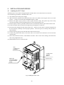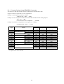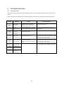
1
YASKAWA
Varispeed SERIES OPTION CARD
PROFIBUS-DP COMMUNICATIONS INTERFACE CARD
USER'S MANUAL
Model: SI-P1
YASKAWA
MANUAL NO. SIBZ-C736-70.9B
INTRODUCTION
This User's Manual describes the operations and specifications of the PROFIBUS Communications
Interface Card (hereafter called the SI-P1 card). The SI-P1 card transfers the data between the Varispeed
series Inverters and the PROFIBUS-DP open-field network (hereafter called the PROFIBUS-DP). Read
this manual carefully and be sure you understand the information provided before attempting any
operations.
For the operation of the Inverter, refer to the instructions of the Varispeed Series Inverters.
General Precautions
・ Some drawings in this manual are shown with the protective cover or shields
removed, in order to describe the detail with more clarity. Make sure all covers
and shields are replaced before operating this product, and operate it in
accordance with the instructions in this manual.
・ This manual may be modified when necessary because of improvement of the
product, modification, or changes in specifications.
・ A new version of the manual will be released under a reviced manual number
when any changes are made.
・ Contact your Yaskawa representative or a Yaskawa office listed on the back of
this manual to order a new manual if this manual is damaged or lost. Please
provide the document number listed on the front cover of this manual when
ordering.
・ Yaskawa cannot guarantee the quality of any products which have been
modified. Yaskawa assumes no responsibility for any injury or damage caused
by a modified product.
1
Safety Information
Read this instruction manual thoroughly before installation, operation, maintenance or inspection of the
PROFIBUS Communications Interface Card SI-P1. In this manual, NOTES FOR SAFE OPERATION
are classified as “WARNING” and “CAUTION.”
WARNING
Indicates a potentially hazardous situation which, if not avoided, could
result in death or serious injury to personnel.
CAUTION
Indicates a potentially hazardous situation which, if not avoided, may
result in minor or moderate injury to personnel and damage to
equipment.
Even items described in
CAUTION
follow these important notes.
may result in a vital acccident in some situations.
In either case,
Receiving
CAUTION
・ Do not use any option card which is damaged or has missing parts.
Failure to observe this caution may result in injury.
Installation and Wiring
WARNING
・ Never touch the inside of the Inverter.
Failure to observe this warning may result in electric shock.
・ Disconnect all power before mounting or removing the option card or wiring. Then wait
at least the specified time (specified on the front cover) after the power supply is
disconnected and all LEDs and CHARGE LED are extinguished.
Failure to observe this warning may result in electric shock.
・ Do not damage or apply excessive stress to the cables. Do not place heavy objects on
the cables or place the cables between other objects.
Failure to observe this warning may result in electric shock, malfunction or damage of the
equipment.
CAUTION
・ Do not touch the elements of the option card with bare hands.
Failure to observe this caution may result in equipment damage caused by static electricity.
・ Insert the connectors firmly.
Failure to observe this caution may result in malfunction or damage of the equipment.
2
Setting
CAUTION
・ Be careful when changing Inverter settings. The Inverter is factory set to suitable
settings.
Failure to observe this caution may result in damage of the equipment.
3
CONTENTS
1. OUTLINE............................................................................................................... 5
2. RECEIVING .......................................................................................................... 6
3. NOMENCLATURE AND SETTING........................................................................ 7
3.1 Components ............................................................................................................................................... 7
3.2 Terminal Block ............................................................................................................................................ 7
3.3 LEDs........................................................................................................................................................... 8
3.4 Address Switch ........................................................................................................................................... 9
3.5 Termination Resistor Selector Switches...................................................................................................... 9
3.6 Transmission Speed Settings ..................................................................................................................... 9
4. INSTALLATION AND WIRING............................................................................. 10
4.1 Installing the SI-P1 Card........................................................................................................................... 10
4.2 Wiring of the Communications Cable.........................................................................................................11
5. FUNCTIONS ....................................................................................................... 14
5.1 Initial Settings ........................................................................................................................................... 14
5.1.1 Inverter Settings ............................................................................................................................... 14
5.1.2 How to Get GSD Files...................................................................................................................... 14
5.2 PROFIBUS-DP Data and I/O Map ............................................................................................................ 15
5.3 High-speed I/O Data ................................................................................................................................. 18
5.4 MEMOBUS Message Area ....................................................................................................................... 19
5.4.1 Configuration of MEMOBUS Command Message ........................................................................... 19
5.4.2 Configuration of MEMOBUS Response Messages .......................................................................... 19
5.4.3 Constant Settings Using MEMOBUS Commands ............................................................................ 19
5.4.4 Handshaking Register...................................................................................................................... 19
5.4.5 Example of Handshaking ................................................................................................................. 19
5.4.6 Flow Chart........................................................................................................................................ 19
6. TROUBLESHOOTING ........................................................................................ 19
6.1 Inverter Errors........................................................................................................................................... 19
6.2 Faults of PROFIBUS-DP Communications LED ....................................................................................... 19
7. SPECIFICATIONS............................................................................................... 19
8. APPENDIX .......................................................................................................... 19
8.1 List of MEMOBUS Registers .................................................................................................................... 19
8.1.1 Command Data (Read and Write).................................................................................................... 19
8.1.2 Status Data (Read Only) .................................................................................................................. 19
8.1.3 Monitor Data (Read Only) ................................................................................................................ 19
8.1.4 Enter Command (Write Only) ........................................................................................................... 19
8.1.5 Inverter Constants (Read and Write)................................................................................................ 19
8.1.6 Error Code ....................................................................................................................................... 19
4
1. OUTLINE
The SI-P1 card is an interface card to achieve data communications with the PROFIBUS-DP master for
connecting the Varispeed series Inverters to the PROFIBUS-DP open field network.
Mounting the SI-P1 card on the Varispeed series Inverter can monitor operation status including running or
stopping; or change or read the settings of the Inverter constants from the PROFIBUS-DP master, which
can be utilised for various types of applications.
The following are the Inverter series on which the SI-P1 card can be mounted.
・Varispeed F7: Standard series, applicable with Inverter software No. S1013 and later
・Varispeed G7: Standard series, applicable with Inverter software No. S1010 and later
5
2. RECEIVING
Check the following items as soon as the product is delivered.
Item
Has the correct model of the
SI-P1 card been delivered?
Is the SI-P1 card damaged in any
way?
Method
Compare the model number on your order to the number
printed in the lower right corner of the SI-P1 card.
(Refer to 3.1.)
Inspect the entire exterior of the SI-P1 card to see if there
are any scratches or any other damage resulting from
shipping.
A GSD file is needed for using the SI-P1 card as a PROFIBUS-DP slave. Use the GSD file to register the
SI-P1 card as a slave to a PROFIBUS-DP master. Contact your Yaskawa representative for more
information how to get a GSD file.
If you find any irregularities, contact the agency from which you purchased the Inverter or your Yaskawa
representative immediately.
6
3. NOMENCLATURE AND SETTING
3.1 Components
The names of components on the SI-P1 card are shown in Fig. 1.
Connector with Inverter
Control Board (JP1)
Status Display LED
PROFIBUS-DP Bus
Connection Terminal
(JP3)
Spacer
Mounting
Hole
Termination Resistor
Selector Switch
Address Switch 2 (×10)
Address Switch 1 (×1)
SI-P1
Ground Lead Wire
73600-C0331
Model and Code No.
Fig. 1 PROFIBUS-DP Communication Interface Card SI-P1
3.2 Terminal Block
This terminal block connects the SI-P1 card to the PROFIBUS-DP communications line.
Terminal
No.
Name
1
2
+5V BUS
GND BUS
3
A-Line
Minus RxD/TxD according to RS-485 specifications
4
B-Line
Plus RxD/TxD according to RS-485 specifications
5
Shield
6
RTS
Shielded connection terminal of bus cable
Not available
Meaning
Not available
Not available
7
1 2 3 4 5 6
Terminal
Block
Termination
Resistor
Selector Switch
3.3 LEDs
These LED indicator lamps indicate the status of the PROFIBUS-DP or the SI-P1 card.
PWR LED
COMM LED
ERR LED
WD LED
LED
Name
Display
PWR
Color
Green
-
Status
Lit
Not lit
COMM
Green
Lit
-
Not lit
Red
Lit
-
Not lit
Green
Lit
Blinking
Lit
Blinking
Not lit
ERR
WD
Red
-
Operation
Status
Power supply ON
Power supply OFF
During communi
cations connected
Communications
error/ power
supply OFF
Communications
error
During
communications
connected/ power
supply OFF
During CPU run
During CPU run
Meaning
Power is supplied to the SI-P1 card from the Inverter.
•Power is not being supplied to the Inverter.
•Incorrect connection of the SI-P1 card does not supply power to
the SI-P1 card.
Normal communications are being carried out between the SI-P1
card and the PROFIBUS-DP master.
•Normal communications are not being carried out between the
SI-P1 card and the PROFIBUS-DP master.
•Power is not being supplied.
An error occurred which disabled PROPFIBUS-DP
communications.
•An SI-P1 card address No. is overlapped.
•The address No. specified by the SI-P1 card is not the same as
that specified by the PROFIBUS-DP master.
•Normal communications are being carried out between the SI-P1
card and the PROFIBUS-DP master.
•Power is not supplied.
SI-P1 card is being initialized.
SI-P1 card is operating normally.
CPU error
CPU error
An error occurred in the SI-P1 card.
An error occurred in the Inverter.
Power supply OFF
Power is not being supplied to the SI-P1 card.
CPU is not operating normally.
8
The SI-P1 card’s
3.4 Address Switch
Rotary address switches to set the slave address on the PROFIBUS-DP are provided.
Use setting address switches 1 and 2 on the SI-P1 card to set the Inverter address on the PROFIBUS-DP.
Address = (address switch 2 setting) × 10 + (address switch 1 setting) × 1
Example) Set the address 15 in using the following procedure.
Set Address switch 2 to 1.
Set Address switch 1 to 5.
9 01
78
4 56
78
9 01
23
Address switch 1
23
Address switch 2
4 56
Set to 5.
Set to 1.
3.5 Termination Resistor Selector Switches
Attach a termination resistor on the final stage of the transmission line to reduce the reflection of the signal
and stabilise the communications. When the SI-P1 card is connected as the last unit for the
communications line, turn ON the termination resistor selector switch of the SI-P1 card to connect the
termination resistor. No termination resistor has to be attached externally.
ON
ON
Provided
(Switch is ON)
1
Not provided
(Switch is OFF)
3.6 Transmission Speed Settings
Setting the transmission speed on the PROFIBUS-DP master automatically sets the same transmission
speed on the SI-P1 card.
9
4. INSTALLATION AND WIRING
4.1 Installing the SI-P1 Card
Install the SI-P1 card is where the digital operator and the front cover of the Inverter are removed.
Use the following procedure to install the SI-P1 card.
(1) Turn off the main-circuit power supply.
(2) Wait at least the specified time (specified on the front cover) before removing the front cover of the
Inverter. Check to be sure that the CHARGE indicator is OFF.
(3) Remove the option clip to prevent C and D option and from rising. The option clip can be easily
removed by holding onto the protruding portion of the clip and pulling it out.
(4) Insert the spacer, which is provided on the Inverter's control board, into the spacer hole of SI-P1 card.
(5) Fit the connector (JP1) on the SI-P1 card precisely to the Option-C connector.
(6) Pass the spacer through the spacer hole on the card. Check to be sure that it is precisely aligned with
the 2CN position, and snap it into the proper position. Be sure to press it in firmly until you hear it
snap into place.
(7) Insert the option clip to prevent the side with connector from rising.
(8) Connect the ground lead cable of the SI-P1 card to the control circuit terminal 12 on the Inverter
control board.
(9) Select the termination resistor, set the address switches 1 and 2 to the correct setting, and connect the
card to the peripheral devices.
(10) Reattach the front cover of the Inverter.
2CN
C Option Card
Connector
C Option Card
mounting
Spacer
C Oprion Card
Option Clip
(To prevent raising
of C and D Option
Cards)
Fig. 2 Installing the SI-P1 Card
10
4.2 Wiring of the Communications Cable
Use the following procedure to wire the PROFIBUS-DP master to the terminal block of the SI-P1 card.
Use a shielded twisted-pair cable in conformance with the PROFIBUS specifications for the
communications cable.
1) The following table shows the applicable cable sizes for the terminal block (JP3).
[Terminal: MINI COMBICON series, manufactured by Phoenix Contact Co., Ltd.]
Standard wire
Single wire
UL
CSA
[mm2]
0.14 to 1.5
0.14 to 1.5
-
-
AWG
28 to 16
28 to 16
30 to 14
28 to 16
I
[A]
8
8
8
8
VAC
[V]
160
160
300
300
2) Refer to Fig. 4.2 for the connection cable termination of the bus connection terminal on the SI-P1
card’s side.
3) Use a thin screwdriver that is less than 2.5 mm wide and less than 0.4 mm thick to loosen the terminal
screw.
4) Connect the No.3 pin on the bus connection terminal block on the SI-P1 card’s side to the No. 8 pin on
the PROFIBUS-DP master D-SUB’s side and connect the No.4 pin on the terminal block on the SI-P1
card’s side to the No. 3 pin on the PROFIBUS-DP master D-SUB’s side. (Refer to Fig. 4.)
5) Insert the wires from under the terminal block.
6) Tighten the terminal screws firmly.
(Tightening torque: 0.22 to 0.25 [N ・ m])
Stripped wire:
approx. 5.5 mm long
Wire
Fig. 3 End of Connection Cable
11
Inverter
Motor
3-phase
Power Supply
PROFIBUS-DP Master
SI-P1 Card
2CN
(60P)
Bus Connection
Terminal Block
1
(JP3)
9-pin
D-SUB
RxD/TxD-N
RxD/TxD-P
2
8
3
3
P
4
5
R
U
S
V
T
W
Varispeed
Series
2CN
(60P)
RxD/TxD-N
RxD/TxD-P
Shield
6
E
E (G)
Notes: 1 A PROFIBUS cable is recommended for the shielded twisted-pair cable.
2
Separate the communications cables from the main circuit wiring or other
power cables.
Fig. 4 Interconnection (when One Inverter Used)
12
M
Motor
Inverter
3-phase
Power
Supply
PROFIBUS-DP Master
SI-P1 Card
2CN
(60P)
Bus
RxD/TxD-P
Terminal
2 Block (JP3)
8
3
U
S
V
T
W
M
Varispeed
Series
1 Connection
9-pin
D-SUB
RxD/TxD-N
R
3
P
2CN
(60P)
RxD/TxD-N
4 RxD/TxD-P
5
Shield
6
E (G)
E
Inverter
R
3-phase
Power
Supply
SI-P1 Card
2CN
(60P)
2
3
P
V
T
W
Varispeed
Series
2CN
(60P)
RxD/TxD-N
4 RxD/TxD-P
5
Shield
6
E
E (G)
Fig. 5 Interconnection (when Two Inverters Used)
13
U
S
1 Bus
Connection
Terminal
Block (JP3)
Motor
M
5. FUNCTIONS
5.1 Initial Settings
5.1.1 Inverter Settings
Set the following constants, whenever necessary, before starting communications between the Inverter and
the PROFIBUS-DP master.
Name
Constant
No.
F7
G7
Set the inputting method for frequency reference.
0: Digital Operator
1: Control circuit terminals (analog inputs)
2: MEMOBUS communication (using SI-K2)
3: Option Card
4: MEMOBUS communication (for CP-717)
1
○
○
Set the operation method.
0: Digital Operator
1: Control circuit terminals (sequence inputs)
2: MEMOBUS communication (using SI-K2)
3: Option Card
4: MEMOBUS communication (for CP-717)
1
○
○
1
○
○
0
○
○
1
○
○
1
×
○
Display
Reference selection *1
b1-01
Reference Source
Operation method selection *1
b1-02
Run Source
Operation selection after
communications error
F6-01
Set the stopping method for communication errors.
0: Deceleration stop using deceleration time in C1-02
1: Coast to stop
BUS Fault Sel
Inverter
Factory
Setting
Description
2: Emergency stop using deceleration time in C1-09
3: Continue operation *2
Input level of external fault from
Communications Option Card
F6-02
EF0 Detection
F6-03
Stopping method for external
fault from Communications
Option Card
EF0 Fault Action
Torque reference/torque limit
selection from optical option
F6-06
Torque Ref/Lmt Sel
0: Always detect
1: Detect during operation
0: Deceleration stop using deceleration time in C1-02.
1: Coast to stop
2: Emergency stop using deceleration C1-09.
3: Continue operation *2
0: Torque reference/torque limit from transmission disabled
1: Torque reference/torque limit from transmission enabled.
*1: Set b1-02 to 3 to run/stop through the PROFIBUS-DP communications. Set b1-01 to 3 to specify the frequency.
*2: Selecting "Continue operation" will allow the operation with the Inverter to continue when a fault occurs.
Provide other measures such as an emergency stop switch for safe operation.
*3: Enabled when A1-02 (Control method selection) is set to 3 (Flux vector) or 4 (open loop vector). In this case, the d5-01
(Torque control selection) setting can be used to select the torque reference or the torque limit.
d5-01 = 0 (Speed control): Torque limit setting
d5-01 = 1 (Torque control): Torque reference setting
*4: When F1-06 is set to 1 (factory setting), the motor may not turns unless the torque reference or the torque limit is set
from the PROFIBUS-DP master.
5.1.2 How to Get GSD Files
A GSD file is needed for using the SI-P1 card as a PROFIBUS-DP slave. Use the GSD file to register the
SI-P1 card as a slave to a PROFIBUS-DP master. Contact your Yaskawa representative for more
information how to get a GSD file.
14
5.2 PROFIBUS-DP Data and I/O Map
Input and output data length of SI-P1 card can be chosen from among Extended data 1 (32 bytes),
Extended data 2 (12 bytes) and Basic data (6 bytes). Data length is set by the configuration tool of
PROFIBUS-DP master.
(1) Extended data 1 (data length: 32 bytes)
z High-speed I/O data – Bytes 0 to 15
This data is directly transferred to the Inverter or from the Inverter.
running or stopping of the Inverter.
z MEMOBUS message – Bytes 16 to 31
Using this high-speed I/O can control
This data is transferred to the Inverter using MEMOBUS messages. All the Inverter constants and data
can be accessed by this data. Because the data in this area is transferred to the Inverter after the SI-P1
card receives and edits it, time is required to return the data. The master must synchronize the timing of
sending and receiving the data by the handshaking.
Also the run command or the frequency reference changes immediately by high-speed I/O even if it is
commanded by MEMOBUS messages.
The following memory map shows the I/O data bytes and their designated functions.
15
Output Data
Input Data
PROFIBUS-DP Master ⇒ Inverter
Byte
0
1
2
3
4
5
6
7
8
9
10
11
12
13
14
15
16
17
18
19
20
21
22
23
24
25
26
27
28
29
30
31
Inverter ⇒ PROFIBUS-DP Master
Function
Run Command
Frequency Reference
Torque Reference / Torque Limit
Torque Compensation
Not used
Multi-function Analog Output 1 (Terminal
FM) Output
Multi-function Analog Output 2 (Terminal
AM) Output
Multi-function Output
Function Code (Reference)
Starting Register No.
Number of Data Items
Data 1
Data 2
Data 3
Data 4
Not used
Handshaking Register
16
Byte
0
1
2
3
4
5
6
7
8
9
10
11
12
13
14
15
16
17
18
19
20
21
22
23
24
25
26
27
28
29
30
31
Function
Inverter Status
Motor Speed
Torque Reference
Speed Detection PG Count Value
Frequency Reference
Output Frequency
Output Current
Main Speed Frequency Reference
(Terminal A2) Input
Function Code (Return)
Starting Register No.
Number of Data Items
Data 1
Data 2
Data 3
Data 4
Not used
Handshaking Register
(2) Extended data 2 (data length: 12 bytes)
z
High-speed I/O data – Bytes 0 to 3
z
MEMOBUS Message – Bytes 4 to 11
Output Data
Input Data
PROFIBUS-DP Master ⇒ Inverter
Byte
0
1
2
3
4
5
6
7
8
9
10
11
Inverter ⇒ PROFIBUS-DP Master
Function
Byte
0
1
2
3
4
5
6
7
8
9
10
11
Run Command
Frequency Reference
Function Code (Reference)
Starting Register No.
Number of Data Items
Data 1
Not used
Handshaking Register
Function
Inverter Status
Motor Speed
Function Code (Return)
Starting Register No.
Number of Data Items
Data 1
Not used
Handshaking Register
(3) Basic data (data length: 6 bytes)
z High-speed I/O data – Bytes 0 to 5
Output Data
Input Data
PROFIBUS-DP Master ⇒ Inverter
Byte
0
1
2
3
4
5
Inverter ⇒ PROFIBUS-DP Master
Function
Byte
0
1
2
3
4
5
Run Command
Frequency Reference
Torque Reference/Torque Limit
17
Function
Inverter Status
Motor Speed
Output Current
5.3 High-speed I/O Data
The data in this area is directly transferred to the Inverter.
PROFIBUS-DP Master ⇒ Inverter
For Extended data 1:
Byte
0
1
2
3
4
5
6
7
8
9
10
11
12
13
14
15
Function
Run Command
Frequency reference
Torque reference /Torque
limit *1, *2
Torque compensation *1
Meaning
Upper byte
Run Command
Lower byte
Upper byte
Frequency
reference
Lower byte
Torque reference/ Upper byte
torque limit value Lower byte
Upper byte
Torque
compensation
Lower byte
Not used
Set to "00H".
Multi-function Analog
Output 1 (Terminal FM) *3
Multi-function Analog
Output 2 (Terminal AM) *3
Not used
Upper byte
Analog output
value
Lower byte
Upper byte
Analog output
value
Lower byte
Set to "00H".
Bit 0: Multi-function contact
output terminals M1 and
M2
Bit 1: Multi-function output 1 –
terminals P1 and PC
Bit 2: Multi-function output 2 terminals P2 and PC
Bit 3 to 7: Set to "0".
Multi-function Output *4
Remarks
Refer to the table5.1.
1 = 0.01 Hz (Unit depends on the o1-03 setting.)
Setting range: zero to maximum frequency
1 = 0.1%
Setting range: F448H (-300.0) to 0BB8H (300.0%)
1 = 0.1%
Setting range: F448H (-300.0) to 0BB8H (300.0%)
F9FCH (-11V) to 0604H (11V)
F9FCH (-11V) to 0604H (11V)
0: Open
1: Closed
*1: Can be used when setting A1-02 (Control method selection) to 3 (Flux vector) or 4 (Open loop vector 2) for Varispeed
G7 series.
*2: Can be used when F6-06 (Torque reference/torque limit selection from optical option) is set to 1. In this case, the
setting of d5-01 (Torque control selection) can be used to select the torque reference or the torque limit.
d5-01 = 0 (Speed control): torque limit value
d5-01 = 1 (Torque control): torque reference value
*3: To select inverter multi-function analog output for communications, set H4-01 [Monitor selection (terminal FM)] and
H4-04 [Monitor selection (terminal AM)] to 31 (Not used).
*4: Inverter multi-function output ON/OFF during communications, set H2-01 [Multi-function input (terminal M1-M2)],
H2-02 [Multi-function output 1 (terminal P1)], and H2-03 [Multi-function output 2 (terminal P2)] to F.
18
Run Command (common to each data length)
Bit No.
0
1
2
Description
FWD run/stop
REV run/stop
Terminal S3 function
3
Terminal S4 function
4
Terminal S5 function
5
Terminal S6 function
6
Terminal S7 function
7
Terminal S8 function *
8
9
A
External fault
Fault reset
B
C
D
E
F
Terminal S9 function *
Terminal S10 function *
Terminal S11 function *
Terminal S12 function *
Fault history trace clear
External BB command
Remarks
Enabled when setting b1-02 (Operation method selection) to 3 (Option card).
Depends on H1-01 (multi-function selection 1: terminal S3 function selection)
setting.
Depends on H1-02 (multi-function selection 2: terminal S4 function selection)
setting.
Depends on H1-03 (multi-function selection 3: terminal S5 function selection)
setting.
Depends on H1-04 (multi-function selection 4: terminal S6 function selection)
setting.
Depends on H1-05 (multi-function selection 5: terminal S7 function selection)
setting.
Depends on H1-06 (multi-function selection 6: terminal S8 function selection)
setting.
1: External fault
1: Fault reset
Depends on H1-07 (multi-function selection 7: terminal S9 function selection)
setting.
Depends on H1-08 (multi-function selection 8: terminal S10 function selection)
setting.
Depends on H1-09 (multi-function selection 9: terminal S11 function selection)
setting.
Depends on H1-10 (multi-function selection 10: terminal S12 function selection)
setting.
1: Clears the fault history.
1: External Baseblock
*: Not used with Varispeed F7 series inverters since they do not have terminals S8 to S12.
19
Inverter ⇒ PROFIBUS-DP Master
For Extended data 1:
Byte
0
1
2
3
4
5
6
7
8
9
10
11
12
13
14
15
Function
Inverter status
Motor speed *1
Torque reference *2
Speed Detection PG Count
Value *3
Frequency reference
Output frequency
Output current
Main Speed Frequency
Reference (Terminal A2) input
*6
Description
Inverter status
16-bit hexadecimal data
16-bit hexadecimal data
16-bit hexadecimal data
16-bit hexadecimal data
16-bit hexadecimal data
16-bit hexadecimal data
16-bit hexadecimal data
Description
upper byte
lower byte
upper byte
lower byte
upper byte
lower byte
upper byte
lower byte
upper byte
lower byte
upper byte
lower byte
upper byte
lower byte
upper byte
lower byte
Refer to the table 5.2.
1 = 0.01 Hz *4
1 = 0.1%
1 = 1 pulse
1 = 0.01 Hz *4
1 = 0.01 Hz *4
1 = 0.01 A *5
1=0.1%
*1: Cannot be used when setting A1-02 (Control method selection) to 0 (V/f control).
*2: Cannot be used when setting A1-02 (Control method selection) to 0 (V/f control) or 1 (V/f with PG feedback).
*3: Can be used when setting A1-02 (Control method selection) to 1 (V/f with PG feed back) or 3 (Flux vector).
*4: Unit depends on the setting of o1-03 (Frequency units of reference setting and monitor).
*5: 1 is 0.1 A for Inverters with a capacity of more than 11 kW.
*6: Inverter analog input status (terminal A2) can be seen.
Inverter Status (common to each data length)
Bit No.
0
1
2
3
4
5
6
7
8
9
A
B
C
D
E
F
Name
Running
Zero Speed
Reverse Running
Reset Signal Being Input
Frequency (Speed) Agree
Inverter Operation Ready
Minor Fault
Major Fault
OPE Error
Recovery From Momentary Power Loss
Enabled/Disabled
LOCAL/REMOTE Selection
Multi-function Output Selection 1
Terminals M1-M2 Output
Multifunction Output Selection 2
Terminals P1-PC Output
Multifunction Output Selection 3
Terminals P1-PC Output
Motor Selection (1/2)
Zero Servo Completed*
Meaning
1: Running (run command ON or voltage output)
1: Zero speed
1: Reverse running
1: Reset signal being input.
1: Frequency (speed) agreed
1: Inverter operation ready.
1: Displayed at warning
1: Alarm
1: Operation error (constant setting error)
0: No recovery after momentary power loss
1: Running after momentary power loss
1: REMOTE selected
1: Closed
1: Closed
1: Closed
1: Motor 2 selected.
1: Zero servo is completed.
*: Can be used when setting A1-02 (Control method selection) to 3 (Flux vector) for Varispeed G7 Series.
20
5.4 MEMOBUS Message Area
In this area, a MEMOBUS message is transferred to the SI-P1 card, and the constants in the Inverter can be
set, read, and monitored. Up to four data items can be written or read at one time.
Because the SI-P1 card edits the MEMOBUS message internally and transfers it to the Inverter after
receiving the message, time is required to return it. It is necessary to synchronize sending or receiving of
the data between the PROFIBUS-DP master and the SI-P1 card. Use the handshaking register for
sychronization. For details on the handshaking register, refer to 5.4.4 "Handshaking Register."
To write a constant to the inverter, be sure to execute an ENTER command. The written data becomes
valid by executing the ENTER command. For the details of the ENTER command, refer to 8.1.1 "Enter
Command."
5.4.1 Configuration of MEMOBUS Command Message
The following table shows the configuration of MEMOBUS command messages when the Extended data 1
is selected.
Byte
Name
Function
MEMOBUS command code:
16
17
18
19
20
21
22
23
24
25
26
27
Function code
Starting Resistor No.
Number of Data Items
03H: Read command (reading Inverter internal data)
10H: Write command (writing data into the inverter)
Other codes: Not supported.
Starting resistor No.
upper byte
lower byte
Write: Set doubled number of written data items (2 to 8).
Read: Set doubled number of read data items (2 to 8).
Data 1*
Data word 1
Data 2*
Data word 2
Data 3*
Data word 3
Data 4*
Data word 4
upper byte
lower byte
upper byte
lower byte
upper byte
lower byte
upper byte
lower byte
28
29
Not used
-
30
31
Handshaking Resistor
Refer to 5.4.4 "Handshaking Register."
*: Setting is needed only for the write command. Always select 00H for the read command.
21
5.4.2 Configuration of MEMOBUS Response Messages
The following table shows the configuration of MEMOBUS response messages when the Extended data 1
is selected.
Byte
16
17
18
19
20
21
22
23
24
25
26
27
Name
Function code
Starting resistor No.
Number of data items
Data 1*
Data 2*
Data 3*
Data 4*
Function
MEMOBUS response codes
00H: Waiting for response from inverter
03H: Response to read operation
10H: Response to write operation
83H: Read command error
90H: Write command error
Other codes: Not supported.
Starting resistor No.
upper byte
lower byte
Write: Set double number of written data items
Read: Set double number of read data items
Data word 1
upper byte
lower byte
Data word 2
upper byte
lower byte
Data word 3
upper byte
lower byte
Data word 4
upper byte
lower byte
28
29
Not used
30
31
Handshaking register
Refer to 5.4.4 "Handshaking Register."
*: Data is returned only for the read command.
22
If an error occurs, the SI-P1 card sets MSB (Most Significant Bit) in the MEMOBUS response code to 1
and returns the error response. The number of data items is set to 02H and the following error codes are
set to the lower bytes of Data 1.
Error Name
Error Code
Description
Function Code Error
01H
Something other than 03H or 10H is specified for the function code.
Incorrect Register No.
02H
Start register No. is greater than the setting of 600H.
Unused register No. is specified.
Improper Number of
Data Items
03H
The number of data items at write-in or read-out is outside the acceptable
range setting of the constant for writing in 2 to 8.
Incorrect Data
Contents
21H
The setting of the constant for writing in is beyond the upper or lower limit of
the constant.
Constant is incorrectly set at constant write-in.
22H
A constant is written during running.
ENTER command is written during running.
Read-only data is written.
23H
A constant is written when the Inverter is undervoltage (UV).
ENTER command is written when the Inverter is undervoltage (UV).
24H
A constant is written while data is being stored.
Incrorrect Write-in
23
5.4.3 Constant Settings Using MEMOBUS Commands
The written or read data of each constant is transferred in a hexadecimal value.
Negative values are expressed as a two's complement.
Example 1) The frequency reference is 30Hz.
30 Hz/0.01 Hz = 3000 → bb8H
Example 2) -5% is assigned as the bias for terminal FM of multi-function analog output 1.
5/0.1 = 50 → 32H
Converted into a two's complement → FFCEH
Example 3) 60.00 Hz is assigned for d1-01 (register No.: 0280H).
60.00Hz/0.01Hz = 6000 → 1770H
Byte
16
17
18
19
20
21
22
23
24
25
26
27
28
29
30
31
Name
Command
Message
10H
02H
80H
02H
17H
70H
00H
00H
00H
00H
00H
00H
00H
00H
00H
01H
Function code
Starting Register No.
Upper
Lower
Number of Data Items
Data 1
Data 2
Data 3
Data 4
Upper
Lower
Upper
Lower
Upper
Lower
Upper
Lower
Not used
Handshaking Resistor *1
*1: Depends on the status of the previous data.
*2:Depends on the status of the fault.
24
Data
Response Response Message
Message
(at Fault) *2
10H
90H
02H
00H
80H
00H
02H
02H
00H
00H
00H
02H
00H
00H
00H
00H
00H
00H
00H
00H
00H
00H
00H
00H
00H
00H
00H
00H
00H
00H
01H
01H
5.4.4 Handshaking Register
Handshaking is used to synchronize the timing of the sending or receiving of MEMOBUS message data
between the SI-P1 card and the PROFIBUS-DP master. Use byte 31 in the PROFIBUS-DP master input
area (from the SI-P1 card to the PROFIBUS-DP master) and in the output area (from the PROFIBUS-DP
master to the SI-P1 card). When the status of byte 31 bit 7 changes, the data set to the output area on the
PROFIBUS master’s side becomes valid on the SI-P1 card. When the status obtained after changing byte
31 bit 7 in the output area coincides with the bit 7 status in the input area, the data in the input area on the
PROFIBUS-DP master’s side must be valid.
Handshaking Output Register
PROFIBUS-DP Master ⇒ SI-P1 Card
b7
HS
Bit
b0
-
-
-
-
-
-
INIT
Name
7
HS
1 to 6
-
0
INIT
Function
Handshaking bit. Used to synchronize the timing for sending or receiving data.
Changes the status when a new command is transmitted.
Note: Be sure to clear this bit to 0 when turning ON the power supply or setting
bit 0 (INIT) to 1 to initialize the handshaking bit for the SI-P1 card.
Not used
Clears the handshaking bit for the SI-P1 card to 0
25
Handshaking Input Register
SI-P1 Card ⇒ PROFIBUS-DP Master
b7
HS
Bit
b0
STATUS
WD
-
Name
Function
Handshaking bit. Used to synchronize the timing for sending or
receiving data. Changes the status when a new response is transmitted.
7
HS
5 to 6
STATUS *
1 to 4
WD *
0
-
Note: This bit is cleared to 0 when the power supply is turned ON or by
setting the handshaking initialization bit (INIT) on the output
register on the PROFIBUS-DP master’s side) to 1.
Status of the data exchange between the PROFIBUS-DP master and the
Inverter.
00H: Idle
01H: Sends a MEMOBUS command to the Inverter.
10H: Waits for a MEMOBUS command from the Inverter.
11H: Receives a response.
Counter increases every 64 ms.
Not used
* STATUS and WD are information for your reference.
26
5.4.5 Example of Handshaking
Clear the handshaking register HS bit (bit 7) to 0 for the PLC program after turning ON the power supply
or re-initialization. The following drawing describes how to perform handshaking. The arrow marks
indicate whether the PROFIBUS-DP master or the SI-P1 card has the control for the protocol.
PROFIBUS-DP Master
SI-P1 Card
Handshaking Output Register Handshaking Input Register
Initial 0
Setting
0
Initial Setting
⇓
Creation of
Command
0
0
⇓
Command
Valid
⇒
1
0
New MEMOBUS Command for SI-P1
Card
⇓
1
0
Processing of Command
⇓
1
⇐
1
Response Valid
1
Idle
1
New MEMOBUS Command to SI-P1 Card
⇓
Creation of
Command
1
Command
Valid
0
⇓
⇒
⇓
0
1
Processing of Command
⇓
0
⇐
0
Response Valid
0
Idle
0
New MEMOBUS Command to SI-P1 Card
⇓
Creation of
Command
0
⇓
Command
Valid
1
⇒
⇓
etc.
27
5.4.6 Flow Chart
The following flow chart shows how handshaking works when a MEMOBUS message is used.
PROFIBUS-DP DP Master
Power ON or
re-initialization
SI-P1 Card
START
START
Clears the handshaking
register HS bit to "0".
NO
Initialization
Clears handshaking
register HS bit to "0".
*: Toggle means to change
the HS bit status from 0
to 1 or from 1 to 0.
Sends a new message.
YES
Creates a command message.
Toggles handshaking
register HS bit.*
Sends to slave.
Receives for the master.
Transfers to dual port RAM.
Command message
Abnormal
Normal
Command executed.
Creates a response message.
Transfers to dual port RAM.
NO
INDATA HS =
Toggles hand-haking
register HS bit.*
YES
Handles the response.
Sends to master.
28
Command not executed.
Creates a response
message of a fault.
6. TROUBLESHOOTING
6.1 Inverter Errors
The following table outlines the faults displayed in the Inverter’s operator and their causes and corrective
actions.
Refer to the Instruction Manuals for any faults displayed in the operator other than those described below.
Display
Meaning
OPE05
Sequence
Select
Option card
selection error
BUS
Option Com
Err
EF0
Opt External
Flt
Option
Communications
Error
External fault
input from
communications
option card
CPF06
Option Error
Option card
connection error
CPF20
Option A/D
Error
Option card A/D
converter error
CPF21
Option CPU
down
CPF22
Option Type
Err
CPF23
Option
DPRAM Err
Communications
Option card self
diagnostic error
Communications
Option card model
code error
Communications
Option card
DPRAM error
Cause
Corrective Action
The Option card was selected as the
frequency reference source by
setting b1-01 to 3, but an Option
card is not connected.
Communications are not established
between the PROFIBUS-DP master
and the inverter.
External fault is input from the
PROFIBUS-DP master.
Connect the Option card to the 2CN connector on
the inverter control board.
The Inverter and the Option card are
not connected properly.
The Inverter and the Option card are
not connected properly.
The option card’s A/D converter is
faulty.
Option card fault
29
Confirm the PROFIBUS-DP communications
LED display.
Turn OFF the external fault input.
Turn OFF the inverter power supply and confirm
the Option card and Inverter connection. Then
turn ON the power supply again.
Replace the Option card if the fault occurs again.
Turn OFF the inverter power supply and confirm
the Option card and Inverter connection. Then
turn ON the power supply again.
Replace the Option card if the fault occurs again.
Turn ON the inverter power supply again.
Replace the Option card if the fault occurs again.
6.2 Faults of PROFIBUS-DP Communications LED
The following table shows the faults, causes and corrective actions to be displayed in the LED on the SI-P1
card.
LED Display
PWR
COMM
ERR
Meaning
WD
Cause
Corrective Action
Power is not supplied to the
inverter.
●
●
●
Power OFF
●
SI-P1 card is not connected
properly so that power is not
supplied to the SI-P1 card.
SI-P1 card CPU is defective.
CPU error
●
Green
Red
Red
Inverter is defective.
Inverter error
●
Green
Red
Red
An error occurred and disabled
communications.
Green
Communications
error
Green
Communications
error
●
Green
Green
Red
Green
Red
●
reen
Green
Green
CPU Initialization
●
Green
Green
Green
Normal
An error occurred and disabled
communications.
Check the inverter main circuit
wiring and turn ON the power
supply.
Turn OFF the inverter power
supply and check the SI-P1 card
and Inverter connection. Then
turn ON the power supply again.
Turn ON the inverter power supply
again. If the fault occurs again,
replace the SI-P1 card.
Turn ON the inverter power supply
again. If the fault occurs again,
replace the Inverter.
Confirm that the address specified
by the PROFIBUS-DP master
coincides with the SI-P1 card
address.
Confirm that the PROFIBUS-DP
master is operating normally.
Confirm that the termination
resistor is connected correctly to the
communications line.
Confirm that the communications
line is connected correctly.
Confirm that the communications
line is separated from the main
circuit wiring.
Confirm that the same address is
not used for other devices in the
PROFIBUS-DP.
SI-P1 card is being initialized.
Normal communications are
enabled.
Note: LED Status
: Lights
: Blinks
30
●
: Not lit
7. SPECIFICATIONS
Item
Model
PROFIBUS Data
Operating Power Supply
Ambient Operating
Temperature
Ambient Operation Humidity
Storage Temperature
Application Site
Altitude
Communications Speed
Specifications
SI-P1
Extended data 1
High-speed I/O data (inputs: 16 bytes, outputs: 16 bytes)
MEMOBUS message (inputs: 16 bytes, outputs: 16 bytes)
Extended data 2
High-speed I/O data (inputs: 4 bytes, outputs: 4 bytes)
MEMOBUS message (inputs: 8 bytes, outputs: 8 bytes)
Basic data
High-speed I/O data (inputs: 6 bytes, outputs: 6 bytes)
4.75V to 5.25VDC (supplied from inverter)
-10℃ to +45℃
95%RH max. (no condensation)
-20℃ to +60℃
Indoors (no corrosive gases, dust, or dirt)
1000 m max.
9.6k bps to 12M bps
31
8. APPENDIX
8.1 List of MEMOBUS Registers
8.1.1 Command Data (Read and Write)
Register No.
0000H
0001H
0002H
0003H
0004H
0005H
0006H
0007H
0008H
0009H
000AH
-
000EH
000FH
Meaning
BIT
Reserved
Run Command
0
Forward run/Stop 1: Forward run 0: Stop
1
Reverse run/Stop 1: Reverse run 0: Stop
2
External fault 1: Fault (EF0)
3
Fault reset 1: Fault reset
4
ComNet
5
ComCtrl
6
Multi-function input reference 3 (terminal S3)
7
Multi-function input reference 4 (terminal S4)
8
Multi-function input reference 5 (terminal S5)
9
Multi-function input reference 6 (terminal S6)
A Multi-function input reference 7 (terminal S7)
B Multi-function input reference 8 (terminal S8)
C Multi-function input reference 9 (terminal S9)
D Multi-function input reference 10 (terminal S10)
E Multi-function input reference 11 (terminal S11)
F Multi-function input reference 12 (terminal S12)
Frequency reference (Unit: set by o1-03)
Not used
Torque reference
Torque compensation
PID aimed value
Analog output 1 setting (-11V/-1540 to 11 V/1540, valid when H4-01 is set to 31)
Analog output 2 setting (-11V/-1540 to 11 V/1540, valid when H4-04 is set to 31)
Multi-function output setting
0
Contact output (terminals M1 and M2) 1: ON 0: OFF
1
PHC1 (terminals P1 and PC) 1: ON 0: OFF
2
PHC2 (terminals P2 and PC) 1: ON 0: OFF
3
PHC3 (terminals P3 and C3) 1: ON 0: OFF
4
PHC4 (terminals P4 and C4) 1: ON 0: OFF
5
Not used
6
Fault contact (terminals MA and MC) depends on the setting of bit 7.
1:ON 0:OFF
7
Fault contact (terminals MA and MC) 1:ON 0:OFF
8-F Not used
Inverter
F7
G7
○
○
○
○
○
○
○
○
○
○
○
○
○
○
○
○
○
○
○
○
○
○
○
○
○
○
×
○
×
○
×
○
×
○
×
○
○
○
―
―
×
○
×
○
○
○
○
○
○
○
○
○
×
×
―
○
○
○
○
○
○
○
○
○
―
○
○
○
○
○
Not used
―
―
Reference selection setting
0
Not used
1
PID aimed value input
○
○
○
○
○
○
○
○
○
○
○
×
○
○
○
○
1: Valid
0: Invalid
2-B Not used
C
D
E
F
1: Simultaneous data terminal S5 input
1: Simultaneous data terminal S6 input
1: Simultaneous data terminal S7 input
1: Simultaneous data terminal S8 input
Note: When writing data into the register, write 0 to the unused bit.
32
1: Valid 0: Invalid
1: Valid 0: Invalid
1: Valid 0: Invalid
1: Valid 0: Invalid
Do not write any data to the reserved register.
8.1.2 Status Data (Read Only)
Register No.
0010H
0011H
0012H
0013H
0014H
0015H
Meaning
BIT Display
Inverter status
1: Running
0
1: Zero speed
1
1: Reverse running
2
1: Reset signal inputting
3
1: Speed agree
4
1: Inverter ready
5
1: Minor fault
6
1: Major fault
7
8-D Not used
1: ComRef status
E
1:
ComCtrl status
F
Operator status
1: OPE occurring
0
1: ERR occurring
1
1: PRG mode
2
3-4 1CN status 00: JVOP-160
5-F Not used
OPE No.
Inverter code F7: 2020H G7: 2050H
Fault contents 1
0
PUF
1
UV1
2
UV2
3
UV3
4
-
5
GF
6
OC
7
OV
8
OH
9
OH1
A
OL1
B
OL2
C
OL3
D
OL4
E
RR
F
RH
Fault contents 2
0
EF3
1
EF4
2
EF5
3
EF6
4
EF7
5
EF8
6
-
7
OS
8
DEV
9
PGO
A
PF
B
LF
C
OH3
D
OPR
E
ERR
F
OH4
01: JVOP-161
Inverter
F7
G7
○
○
○
○
○
○
○
○
○
○
○
○
○
○
○
○
○
○
-
-
○
○
○
○
○
○
○
○
-
-
○
○
11: PC
-
○
-
○
○
○
Fuse blown
Main circuit undervoltage / main circuit MC operation error
Control power fault
Inrush prevention circuit fault
Not used
Ground fault
Overcurrent
Main circuit Overvoltage
Cooling fan overheat
/ Cooling fan stop in inverter
Motor overload
Inverter overload
Overtorque 1
Overtorque 2
Internal braking transistor fault
Installed braking resistor overheating
○
○
○
○
○
-
○
○
○
○
○
○
○
○
○
○
○
○
○
○
○
○
-
○
○
○
○
○
○
○
○
○
○
○
External fault (input terminal S3)
External fault (input terminal S4)
External fault (input terminal S5)
External fault (input terminal S6)
External fault (input terminal S7)
External fault (input terminal S8)
Not used
Overspeed
Excessive speed deviation
PG disconnection detected
Main circuit voltage fault
Output open phase
Motor overheat alarm
Operator connection fault
EEPROM write error
Motor overheating
○
○
○
○
○
×
-
○
○
○
○
○
○
○
○
○
○
○
○
○
○
○
-
○
○
○
○
○
○
○
○
○
33
Register No.
0016H
Meaning
BIT Display
Fault contents 3
CE MEMOBUS communications error
0
1
BUS SI-P1 communications error
2
- Not used
3
- Not used
CF Control fault
4
SVE Zero servo fault
5
6
EFO External fault input from communications card
7
FBL PID control feedback command loss
8
UL3 Undertorque detection 1
9
A
B
C
D
E
0017H
0018H
0019H
Inverter
F7
G7
○
○
○
○
○
○
-
-
-
-
○
○
×
○
○
○
○
○
○
○
UL4 Undertorque detection 2
OL7 High-slip braking OL
○
○
○
EF9 External fault (input terminal S9)
EF10 External fault (input terminal S10)
×
○
×
○
EF11 External fault (input terminal S11)
EF12 External fault (input terminal S12)
×
○
×
○
○
○
○
-
-
○
○
○
○
○
-
○
○
○
○
○
-
○
○
○
○
○
○
○
○
○
○
○
○
○
○
×
-
○
○
-
-
○
○
○
○
○
-
○
○
○
○
○
-
○
○
○
○
○
○
○
○
○
○
○
○
○
○
○
-
○
F
CPF Hardware fault
CPF contents 1
Not used
0
Not used
1
CPF02 occurring
2
CPF03 occurring
3
CPF04 occurring
4
CPF05 occurring
5
CPF06 occurring
6
7-F Not used
CPF contents 2
CPF20 occurring
0
CPF21 occurring
1
CPF22 occurring
2
CPF23 occurring
3
Not
used
4-F
Minor fault contents 1
UV Main circuit undervoltage
0
OV Main circuit overvoltage
1
OH Cooling fin overheating
2
OH2 Inverter overheating pre-alarm
3
OL3 Overtorque 1
4
OL4 Overtorque 2
5
EF FWD/REV run command input together
6
BB External baseblock
7
EF3 External fault (input terminal S3)
8
EF4 External fault (input terminal S4)
9
EF5 External fault (input terminal S5)
A
EF6 External fault (input terminal S6)
B
EF7 External fault (input terminal S7)
C
EF8 External fault (input terminal S8)
D
E
- Not used
OS
Overspeed
F
34
○
Register No.
001AH
001BH
0020H
Meaning
BIT
Display
Minor fault 2
0
DEV Excessive speed deviation
1
PGO PG disconnection
2
OPR Digital operator connection fault
3
CE MEMOBUS communications error
4
BUS SI-P1 communications error
5
CALL Waiting for communications
6
OL1 Motor overload
7
OL2 Inverter overload
8
- Not used
9
EFO SI-P1 external fault detecting
A
- Motor switching during running
B
FBL PID feedback reference lost
C
CALL Communications on standby
D
UL3 Undertorque 1
E
UL4 Undertorque 2
F
SE Sequence Error
Minor fault 3
0
- Not used
1
OH3 Motor overheating alarm
2
EF9 External fault (input terminal S9)
3
EF10 External fault (input terminal S10)
4
EF11 External fault (input terminal S11)
5
EF12 External fault (input terminal S12)
6-F
- Not used
Inverter status
0
1: Running
1
1: Reverse running
2
1: Inverter ready
3
1: Fault
4
1: Data setting error
5
1: Multi-function contact output (M1 and M2) ON
6 1: Multi-function PHC1 output (P1 and PC)
7 1: Multi-function PHC2 output (P2 and PC)
8 1: Multi-function PHC3 output (P3 and C3)
9 1: Multi-function PHC4 output (P4 and C4)
A-F Not used
35
Inverter
F7
G7
○
○
○
○
○
○
○
○
○
○
○
○
○
○
○
○
○
○
-
-
○
○
○
○
○
○
○
○
○
○
○
○
○
○
-
○
×
×
×
×
-
○
○
○
○
○
○
○
○
○
×
×
-
-
○
○
○
○
○
-
○
○
○
○
○
○
○
○
○
○
○
-
Register No.
0021H
0022H
0023H
0024H
0025H
0026H
0027H
0028H
0029H
002AH
002BH
Meaning
BIT
Display
Fault contents
0
Overcurrent (OC), ground fault (GF)
1
Main circuit overvoltage (OV)
2
Inverter overload (OL2)
3
Radiation fan overheating, inverter internal cooling fan stop [OH (OH1)]
4
Internal braking transistor fault (rr), installed braking resistor overheating (RH)
5
Fuse blown (PUF)
6
PID control feedback command loss (FBL)
7
External fault (EF0, EF3 to EF7)
8
Hardware fault (CPF)
9
Motor overload (OL1), overtorque detection 1 (OL3), overtorque detection 2
(OL4)
A PG disconnection (PGO), Overspeed (OS), excessive speed deviation (DEV)
B Main circuit undervoltage (UV) detecting
Main circuit undervoltage, main circuit MC operation fault (UV1), control power
C
fault (UV2), inrush prevention circuit fault (UV3)
D Output open phase (LF)
E MEMOBUS communications error
F Operator connection fault (OPR)
Data Link Status
0
Data writing
1
Not used
2
Not used
3
Upper/lower limit error
4
Data consistency error
5-F Not used
Frequency reference (U1-01)
Output frequency (U1-02)
Output voltage reference (U1-06)
Output current (U1-03)
Output power (U1-08)
Torque reference (U1-09)
Not used
Not used
Sequence input status
0 1: Multi-function contact input terminal S1 ON
1 1: Multi-function contact input terminal S2 ON
2 1: Multi-function contact input terminal S3 ON
3 1: Multi-function contact input terminal S4 ON
4 1: Multi-function contact input terminal S5 ON
5 1: Multi-function contact input terminal S6 ON
6 1: Multi-function contact input terminal S7 ON
7 1: Multi-function contact input terminal S8 ON
8 1: Multi-function contact input terminal S9 ON
9 1: Multi-function contact input terminal S10 ON
A 1: Multi-function contact input terminal S11 ON
B 1: Multi-function contact input terminal S12 ON
C-F Not used
36
Inverter
F7
G7
○
○
○
○
○
○
○
○
○
○
○
○
○
○
○
○
○
○
○
○
○
○
○
○
○
○
○
○
○
○
○
○
○
-
-
○
○
-
○
○
○
○
○
○
-
-
○
○
○
○
○
○
○
○
×
×
×
×
×
-
○
○
○
○
○
-
-
○
○
-
○
○
○
○
○
○
-
-
○
○
○
○
○
○
○
○
○
○
○
○
○
-
Register No.
002CH
002DH
002EH
-0030H
0031H
0032H
0033H
0034H
-0037H
0038H
0039H
003AH
003BH
003CH
003DH
003EH
003FH
Meaning
BIT
Display
Inverter status
0
1: Running
1
1: Zero speed
2
1: Speed agree
3
1: Arbitrary speed agree
4
Frequency detection 1 1: Output frequency ≦ L4-01
5
Frequency detection 2 1: Output frequency ≧ L4-01
6
1: Inverter ready
7
1: Undervoltage detection
8
1: Baseblocking
9
Frequency mode 1: Other than communications 0: Communications
A Run command mode 1: Other than communications 0: Communications
B 1: Overtorque detection
C 1: Frequency reference loss
D 1: Fault retry
E
1: Fault occurring
F
1: MEMOBUS time over
Multi-function output status
0
Multi-function contact output (M1 and M2) ON
1
Multi-function PHC output (P1 and PC) ON
2
Multi-function PHC output (P2 and PC) ON
3
Multi-function PHC output (P3 and C3) ON
4
Multi-function PHC output (P4 and C4) ON
5-F Not used
Not used
Inverter
F7
G7
○
○
○
○
○
○
○
○
○
○
○
○
○
○
○
○
○
○
○
○
○
○
○
○
○
○
○
○
○
○
○
○
○
○
○
○
○
○
○
○
○
○
×
○
×
○
-
-
-
-
Main circuit DC bus voltage
Torque monitor
Output power
Not used
○
○
○
-
○
○
○
-
PID control feedback
PID input volume
PID output volume
Software No. (CPU)
Software No. (FLASH)
Communications error contents
0
CRC error
1
Incorrect data length
2
Not used
3
Parity error
4
Overrun error
5
Framing error
6 Time over
7-F Not used
kVA setting
Control mode
○
○
○
○
○
○
○
○
○
○
○
○
○
-
○
○
○
○
-
○
○
○
-
○
○
○
○
-
○
○
37
8.1.3 Monitor Data (Read Only)
For details, refer to the Varispeed Instruction Manuals. The units to be monitored are the same as the operator
displayed units excluding the units related to frequency and output current.
Status Monitor (U1-XX)
Register No.
Contents
Constant
No.
0040H
0041H
0042H
0043H
0044H
0045H
0046H
0047H
0048H
U1-01
U1-02
U1-03
U1-04
U1-05
U1-06
U1-07
U1-08
U1-09
0049H
U1-10
004AH
U1-11
004BH
U1-12
004CH
004DH
004EH
004FH
0050H
U1-13
U1-14
U1-15
U1-16
U1-17
BIT
Frequency reference*1
Output frequency*1
Output current (100%/8192)*2
Control mode
Motor speed*1
Output voltage reference
Main circuit DC bus voltage
Output power
Torque reference (internal)
Input terminal status
0 1: Control circuit terminal S1 closed
1 1: Control circuit terminal S2 closed
2 1: Control circuit terminal S3 closed
3 1: Control circuit terminal S4 closed
4 1: Control circuit terminal S5 closed
5 1: Control circuit terminal S6 closed
6 1: Control circuit terminal S7 closed
7 1: Control circuit terminal S8 closed
8 1: Control circuit terminal S9 closed
9 1: Control circuit terminal S10 closed
A 1: Control circuit terminal S11 closed
B 1: Control circuit terminal S12 closed
C-F Not used
Output terminal status
0 1: Control circuit terminal M1 and M2 closed
1 1: Control circuit terminal P1 closed
2 1: Control circuit terminal P2 closed
3 1: Control circuit terminal P3 closed
4 1: Control circuit terminal P4 closed
5-6 Not used
7 1: Terminal MA/MB and MC closed
8-F Not used
Operation status
0 1: Running
1 1: Zero speed
2 1: Reverse running
3 1: Reset signal inputting
4 1: Speed agree
5 1: Inverter ready
6 1: Minor fault
7 1: Major fault
8 Not used
Cumulative operation time
Software No. (FLASH)
Frequency reference terminal A1 input voltage
Multi-function analog input terminal A2 input voltage
Multi-function analog input terminal A3 input voltage
38
Inverter
F7
G7
○
○
○
○
○
○
○
○
○
○
○
○
○
○
○
○
○
×
×
×
×
×
-
○
○
○
○
×
×
-
○
-
○
○
○
○
○
○
○
○
○
-
○
○
○
○
×
○
○
○
○
○
○
○
○
○
○
○
○
○
○
○
○
○
○
○
○
○
○
-
○
○
○
○
○
○
-
○
-
○
○
○
○
○
○
○
○
○
-
○
○
○
○
○
Register No.
Meaning
Constant
No.
BIT
Inverter
F7
G7
0051H
0052H
U1-18 Motor secondary current (Iq)
U1-19 Motor exciting current (Id)
0053H
U1-20 Output frequency after soft-start*1
○
○
0054H
0055H
0056H
0057H
0058H
0059H
005AH
005BH
005DH
005EH
005FH
0060H
0061H
0062H
0063H
0064H
0065H
U1-21
U1-22
U1-24
U1-25
U1-26
U1-27
U1-28
U1-32
U1-33
U1-34
U1-35
U1-36
U1-37
U1-38
0066H
U1-39
0067H
0069H
006AH
006BH
006CH
U1-40
U1-42
U1-43
U1-44
U1-45
○
○
-
○
×
○
○
○
-
-
○
○
○
×
○
○
○
○
○
○
-
○
○
○
○
-
○
×
×
×
×
○
○
-
○
○
○
○
○
-
-
○
○
○
○
○
○
○
○
○
○
-
○
○
○
○
-
○
○
○
○
○
○
○
Speed control (ASR) input
Speed control (ASR) output
Not used
PID control feedback
DI-16H2 input status
Output voltage reference (Vq)
Output voltage reference (Vd)
Software No. (CPU)
Not used
Not used
ACR output of q axis
ACR output of d axis
OPE fault constant
Zero servo movement pulses
PID input volume
PID output volume
PID command
MEMOBUS communications error code
0 1: CRC error
1 1: Incorrect data length
2 Not used
3 1: Parity error
4 1: Overrun error
5 1: Framing error
6 1: Time over
7-F Not used
Cooling fan operating time
Motor magnetic flux calculated value
Motor magnetic flux current compensated value
Speed control (ASR) output (without filter)
Feed-forward control output
○
○
*1: The unit of frequency is 0.1 Hz with sign when command code 100FH/200FH bit 0 is set to 0.
The unit of frequency depends on the o1-03 setting without a sign when command code 100FH/200FH bit 0 is set to 1.
*2: Output current is 100%/1892. 100% indicates the inverter rated current.
39
Status Monitor (U2-XX)
Register No.
Meaning
Constant
No.
0080H
0081H
0082H
0083H
0084H
0085H
0086H
0087H
0088H
0089H
U2-01
U2-02
U2-03
U2-04
U2-05
U2-06
U2-07
U2-08
U2-09
U2-10
008AH
U2-11
008BH
U2-12
008CH
U2-13
008DH
U2-14
BIT
Current fault (Refer to the next page for Fault Codes.)
Last fault (Refer to the next page for Fault Codes.)
Frequency reference at fault
Output frequency at fault
Output current at fault
Motor speed at fault
Output voltage reference at fault
DC bus voltage at fault
Output power at fault
Torque reference at fault
Input terminal status at fault
0 1: Control circuit terminal S1 closed
1 1: Control circuit terminal S2 closed
2 1: Control circuit terminal S3 closed
3 1: Control circuit terminal S4 closed
4 1: Control circuit terminal S5 closed
5 1: Control circuit terminal S6 closed
6 1: Control circuit terminal S7 closed
7 1: Control circuit terminal S8 closed
8 1: Control circuit terminal S9 closed
9 1: Control circuit terminal S10 closed
A 1: Control circuit terminal S11 closed
B 1: Control circuit terminal S12 closed
C-F Not used
Output terminal status at fault
0 1: Control circuit terminals M1 and M2 closed
1 1: Control circuit terminal P1 closed
2 1: Control circuit terminal P2 closed
3 1: Control circuit terminal P3 closed
4 1: Control circuit terminal P4 closed
5-6 Not used
7 1: Terminal MA/MB and MC closed
8 Not used
Operation status at fault
0 1: Running
1 1: Zero speed
2 1: Reverse running
3 1: Reset signal inputting
4 1: Speed agree
5 1: Inverter ready
6 1: Minor fault
7 1: Major fault
8 Not used
Cumulative operation time at fault
Inverter
F7
G7
○
○
○
○
○
○
○
○
○
○
○
○
○
○
○
○
○
○
×
×
×
×
×
-
○
○
○
○
×
×
-
○
-
○
○
○
○
○
○
○
○
○
-
○
○
○
○
○
○
○
○
○
○
○
○
○
○
○
○
○
○
○
○
○
○
○
○
-
○
○
○
○
○
○
-
○
-
○
○
○
○
○
○
○
○
○
-
○
Fault History (U3-XX)
Register No.
Constant
No.
0090H
0091H
0092H
0093H
0094H
0095H
0096H
0097H
U3-01
U3-02
U3-03
U3-04
U3-05
U3-06
U3-07
U3-08
Meaning
Most recent fault (Refer to the table for Fault Codes.)
Second most recent fault (Refer to the table for Fault Codes.)
Third most recent fault (Refer to the table for Fault Codes.)
Fourth most recent or oldest fault (Refer to the table for Fault Codes.)
Cumulative operation time at fault
Accumulated time of second fault
Accumulated time of third fault
Accumulated time of fourth/oldest fault
40
Inverter
F7
G7
○
○
○
○
○
○
○
○
○
○
○
○
○
○
○
○
Fault Codes of 0080, 0081, 0090 to 0093
Display
PUF
UV1
UV2
UV3
GF
OC
OV
OH
OH1
OL1
OL2
OL3
OL4
RR
RH
EF3
EF4
EF5
EF6
EF7
EF8
OS
DEV
PGO
PF
LF
OPR
ERR
CE
BUS
CF
SVE
EFO
FBL
UL3
UL4
OL7
EF9
EF10
EF11
EF12
VCF
Meaning
Fault Code
Fuse blown
Main circuit undervoltge
Control power fault
Inrush prevention circuit fault
Not used
Ground fault
Overcurrent
Overvoltage
Cooling fan overheating / inverter internal
cooling fan overheating
01H
02H
03H
04H
05H
06H
07H
08H
09H
0AH
0BH
0CH
0DH
0EH
0FH
10H
11H
12H
13H
14H
15H
16H
17H
18H
19H
1AH
1BH
1CH
1EH
1FH
21H
22H
23H
24H
25H
26H
27H
28H
29H
2AH
2BH
2CH
2DH
2EH
2FH
30H
31H
Motor overload
Inverter overload
Overtorque 1
Overtorque 2
Internal braking transistor fault
Installed braking resistor overheating
External fault (input terminal S3)
External fault (input terminal S4)
External fault (input terminal S5)
External fault (input terminal S6)
External fault (input terminal S7)
External fault (input terminal S8)
Not used
Overspeed
Excessive speed deviation
PG disconnection detected
Main circuit voltage fault
Output open-phase
Digital operator connection fault
EEPROM write error
MEMOBUS communications error
SI-P1 communications error
Not used
Not used
Control fault
Zero servo fault
External fault from SI-P1
PID control feedback command loss
Undertorque 1
Undertorque 2
High-slip braking OL
External fault (input terminal S9)
External fault (input terminal S10)
External fault (input terminal S11)
External fault (input terminal S12)
Not used
DC bus neutral overvoltage
41
Inverter
F7
G7
○
○
○
○
○
○
○
○
-
-
○
○
○
○
○
○
○
○
○
○
○
○
○
○
○
○
○
○
○
○
○
○
○
○
○
○
○
○
○
○
○
○
×
○
-
-
○
○
○
○
○
○
○
○
○
○
○
○
○
○
○
○
○
○
-
-
-
-
○
○
×
○
○
○
○
○
×
○
×
○
×
○
×
○
×
○
×
○
×
○
-
-
×
○
8.1.4 Enter Command (Write Only)
Register No.
0900H
0910H
Name
Contents
Writes in constant data to non-volatile memory
Enter command
(EEPROM).
Does not write in constant data to non-volatile
Enter command
memory (EEPROM).
Set Value
0000H
0000H
Enter Command
To write in a constant to the inverter from the PROFIBUS-DP master, be sure to send an Enter command.
The written set value becomes valid when the inverter receives the Enter command. There are two types
of Enter commands as described below.
Enter command that writes in a constant to the non-volatile memory
This command is executed by writing "0" to register number 0900H. When this command is executed,
the changed set value is written in to the non-volatile memory and becomes valid. The value is stored in
the inverter even after the power supply is turned OFF. However, the data can be written in to the
inverter's non-volatile memory at most 100,000 times. So do not use this Enter command unnecessarily.
Enter command that does not write in a constant to the non-volatile memory
This command is executed by writing "0" to register number 0910H. When this command is executed,
the changed set value is not written in to the non-volatile memory and becomes valid. The value is
eliminated and returned to its original value when the power supply is turned OFF. Therefore, use this
command when the set value of a constant is to be changed temporarily.
Register numbers 0900H and 0910H are exclusive for writing.
"Incorrect fault No." (error code 02H) occurs.
42
If any of these registers is read out,
8.1.5 Inverter Constants (Read and Write)
Register No.
0100H
0101H
0102H
0103H
0104H
0105H
Constant
No.
Name
Language selection for digital operator display
Constant access level
Control method selection
Initialize
Password
Password setting
F7
○
○
○
○
○
○
G7
○
○
○
○
○
○
User setting constants
○
○
○
○
○
○
×
○
○
○
○
○
○
○
○
○
○
○
○
○
○
○
○
○
○
○
○
○
○
○
○
○
○
○
○
○
○
○
○
○
○
○
○
○
○
○
○
○
○
○
○
○
○
○
○
○
○
○
○
○
○
○
○
○
○
○
○
○
○
○
○
○
0180H
0181H
0182H
0183H
0184H
0185H
0186H
0187H
A1-00
A1-01
A1-02
A1-03
A1-04
A1-05
A2-01
to 32
b1-01
b1-02
b1-03
b1-04
b1-05
b1-06
b1-07
b1-08
0189H
018AH
018BH
018CH
0191H
0192H
0193H
0195H
01A3H
01A4H
b2-01
b2-02
b2-03
b2-04
b3-01
b3-02
b3-03
b3-05
b4-01
b4-02
Reference selection
Operation method selection
Stopping method selection
Prohibition of reverse operation
Operation selection for setting E1-09 or less
Read sequence input twice
Operation selection after switching to remote mode
Run command selection in programming mode
Zero speed level (DC injection braking starting frequency)
DC injection braking current
DC injection braking time at start
DC injection braking time at stop
Speed search selection
Speed search operating current
Speed search deceleration time
Speed search wait time
Timer function ON-delay time
Timer function OFF-delay time
01A5H
01A6H
01A7H
01A8H
01A9H
01AAH
01ABH
01ACH
01ADH
01AEH
01AFH
01B0H
01B1H
01B2H
01B3H
01B4H
01B5H
b5-01
b5-02
b5-03
b5-04
b5-05
b5-06
b5-07
b5-08
b5-09
b5-10
b5-11
b5-12
b5-13
b5-14
b5-15
b5-16
b5-17
PID control mode selection
Proportional gain (P)
Integral (I) time
Integral (I) limit
Derivative (D) time
PID limit
PID offset adjustment
PID primary delay time constant
PID output characteristics selection
PID output gain
PID reverse output selection
Selection of PID feedback command loss detection
PID feedback command loss detection level
PID feedback command loss detection time
PID sleep function operation level
PID sleep operation delay time
Acceleration/deceleration time for PID reference
0106H-0125H
Inverter
43
Register No.
Constant
No.
01B6H
01B7H
01B8H
01B9H
01CAH
01CBH
01CCH
01CDH
01CEH
01CFH
01D0H
01D1H
01DAH
01DBH
0200H
0201H
0202H
0203H
0204H
0205H
0206H
0207H
0208H
0209H
020AH
020BH
020CH
020DH
020EH
020FH
0210H
0211H
0212H
0213H
0215H
0216H
021BH
021CH
021DH
021EH
021FH
0220H
0221H
0222H
0223H
0224H
0225H
0226H
0227H
022DH
b6-01
b6-02
b6-03
b6-04
b7-01
b7-02
b8-01
b8-02
b8-03
b8-04
b8-05
b8-06
b9-01
b9-02
C1-01
C1-02
C1-03
C1-04
C1-05
C1-06
C1-07
C1-08
C1-09
C1-10
C1-11
C2-01
C2-02
C2-03
C2-04
C3-01
C3-02
C3-03
C3-04
C3-05
C4-01
C4-02
C5-01
C5-02
C5-03
C5-04
C5-05
C5-06
C5-07
C5-08
C6-01
C6-02
C6-03
C6-04
C6-05
C6-11
Name
Dwell frequency at start
Dwell time at start
Dwell frequency at stop
Dwell time at stop
Droop control gain
Droop control delay time
Energy-saving mode selection
Energy-saving gain
Energy-saving filter time constant
Energy-saving coefficient
Power detection filter time constant
Search operation voltage limiter
Zero-servo gain
Zero-servo completion width
Acceleration time 1
Deceleration time 1
Acceleration time 2
Deceleration time 2
Acceleration time 3
Deceleration time 3
Acceleration time 4
Deceleration time 4
Emergency stop time
Accel/decel time setting unit
Accel/decel time switching frequency
S-curve characteristic time at acceleration start
S-curve characteristic time at acceleration end
S-curve characteristic time at deceleration start
S-curve characteristic time at deceleration end
Slip compensation gain
Slip compensation primary delay time
Slip compensation limit
Slip compensation selection during regeneration
Output voltage limit operation selection
Torque compensation gain
Torque compensation primary delay time constant
ASR proportional (P) gain 1
ASR integral (I) time 1
ASR proportional (P) gain 2
ASR integral (I) time 2
ASR limit
ASR primary delay time
ASR switching frequency
ASR integral (I) limit
CT/VT selection
Carrier frequency selection
Carrier frequency upper limit
Carrier frequency lower limit
Carrier frequency proportional gain
Carrier frequency selection for open-loop vector control 2
44
Inverter
F7
○
○
○
○
×
×
○
○
○
○
○
○
×
×
○
○
○
○
○
○
○
○
○
○
○
○
○
○
○
○
○
○
○
○
○
○
○
○
○
○
○
×
×
×
○
○
○
○
○
×
G7
○
○
○
○
○
○
○
○
○
○
○
○
○
○
○
○
○
○
○
○
○
○
○
○
○
○
○
○
○
○
○
○
○
○
○
○
○
○
○
○
○
○
○
○
×
○
○
○
○
○
Register No.
Constant
No.
0280H
0281H
0282H
0283H
0284H
0285H
0286H
0287H
0288H
028BH
028CH
028DH
028EH
028FH
0290H
0291H
0292H
0289H
028AH
0293H
0294H
0295H
0296H
0297H
0298H
0299H
029AH
029BH
029CH
029DH
029EH
029FH
02A0H
02A1H
02A2H
02A4H
d1-01
d1-02
d1-03
d1-04
d1-05
d1-06
d1-07
d1-08
d1-09
d1-10
d1-11
d1-12
d1-13
d1-14
d1-15
d1-16
d1-17
d2-01
d2-02
d2-03
d3-01
d3-02
d3-03
d3-04
d4-01
d4-02
d5-01
d5-02
d5-03
d5-04
d5-05
d5-06
d6-01
d6-02
d6-03
d6-05
Name
Frequency reference 1
Frequency reference 2
Frequency reference 3
Frequency reference 4
Frequency reference 5
Frequency reference 6
Frequency reference 7
Frequency reference 8
Frequency reference 9
Frequency reference 10
Frequency reference 11
Frequency reference 12
Frequency reference 13
Frequency reference 14
Frequency reference 15
Frequency reference 16
Jog frequency reference
Frequency reference upper limit
Frequency reference lower limit
Master speed reference lower limit
Jump frequency 1
Jump frequency 2
Jump frequency 3
Jump frequency width
Frequency reference hold function selection
+ - Speed limits
Torque control selection
Torque reference delay time
Speed limit selection
Speed limit
Speed limit bias
Speed/torque control switching timer
Field weakening level
Field frequency
Field forcing function selection
AφR time constant
45
Inverter
F7
○
○
○
○
○
○
○
○
○
○
○
○
○
○
○
○
○
○
○
○
○
○
○
○
○
○
×
×
×
×
×
×
○
○
×
×
G7
○
○
○
○
○
○
○
○
○
○
○
○
○
○
○
○
○
○
○
○
○
○
○
○
○
○
○
○
○
○
○
○
○
○
○
○
Register No.
Constant
No.
0300H
0302H
0303H
0304H
0305H
0306H
0307H
0308H
0309H
030AH
030BH
030CH
030EH
030FH
0310H
0311H
0312H
0313H
0314H
0315H
0316H
0317H
0318H
0319H
031AH
031BH
031CH
031DH
031EH
031FH
0320H
0321H
0322H
0323H
0324H
0325H
0326H
0327H
E1-01
E1-03
E1-04
E1-05
E1-06
E1-07
E1-08
E1-09
E1-10
E1-11
E1-12
E1-13
E2-01
E2-02
E2-03
E2-04
E2-05
E2-06
E2-07
E2-08
E2-09
E2-10
E2-11
E3-01
E3-02
E3-03
E3-04
E3-05
E3-06
E3-07
E3-08
E4-01
E4-02
E4-03
E4-04
E4-05
E4-06
E4-07
Name
Input voltage setting
V/f pattern selection
Max. output frequency
Max. voltage
Base frequency
Mid. output frequency
Mid. output frequency voltage
Min. output frequency
Min. output frequency voltage
Mid. output frequency 2
Mid. output frequency voltage 2
Base voltage
Motor rated current
Motor rated slip
Motor no-load current
Number of motor poles
Motor line-to-line resistance
Motor leak inductance
Motor iron saturation coefficient 1
Motor iron saturation coefficient 2
Motor mechanical loss
Motor iron loss for torque compensation
Motor rated output
Motor 2 control method selection
Motor 2 max. output frequency
Motor 2 max. voltage
Motor 2 max. voltage frequency
Motor 2 mid. output frequency
Motor 2 mid. output frequency voltage
Motor 2 min. output frequency
Motor 2 min. output frequency voltage
Motor 2 rated current
Motor 2 rated slip
Motor 2 no-load current
Motor 2 number of poles
Motor 2 line-to-line resistance
Motor 2 leak inductance
Motor 2 rated capacity
46
Inverter
F7
○
○
○
○
○
○
○
○
○
○
○
○
○
○
○
○
○
○
○
○
×
○
○
○
○
○
○
○
○
○
○
○
○
○
○
○
○
○
G7
○
○
○
○
○
○
○
○
○
○
○
○
○
○
○
○
○
○
○
○
○
○
○
○
○
○
○
○
○
○
○
○
○
○
○
○
○
○
Register No.
Constant
No.
0380H
0381H
0382H
0383H
0384H
0385H
0386H
0387H
0388H
0389H
038AH
038BH
038CH
038DH
038FH
0390H
0391H
0392H
0393H
0394H
0395H
0396H
0397H
0398H
0399H
039AH
039BH
039CH
039DH
039EH
039FH
03A0H
03A1H
03A2H
03A3H
03A4H
03A5H
03A7H
F1-01
F1-02
F1-03
F1-04
F1-05
F1-06
F1-07
F1-08
F1-09
F1-10
F1-11
F1-12
F1-13
F1-14
F2-01
F3-01
F4-01
F4-02
F4-03
F4-04
F4-05
F4-06
F4-07
F4-08
F5-01
F5-02
F5-03
F5-04
F5-05
F5-06
F5-07
F5-08
F5-09
F6-01
F6-02
F6-03
F6-04
F6-06
Name
PG constant
Operation selection at PG open circuit (PGo)
Operation selection at Overspeed (oS)
Operation selection at deviation (dEv)
PG rotation
PG division rate (PG pulse monitor)
Integral value during accel/decel enable/disable
Overspeed detection level
Overspeed detection delay time
Excessive speed deviation detection level
Excessive speed deviation detection delay time
Number of PG gear teeth 1
Number of PG gear teeth 2
PG open-circuit detection time
Bi-polar or uni-polar input selection
Digital input option
Channel 1 monitor selection
Channel 1 gain
Channel 2 monitor selection
Channel 2 gain
Channel 1 output monitor bias
Channel 2 output monitor bias
Analog output signal level for channel 1
Analog output signal level for channel 2
Channel 1 output selection
Channel 2 output selection
Channel 3 output selection
Channel 4 output selection
Channel 5 output selection
Channel 6 output selection
Channel 7 output selection
Channel 8 output selection
DO-08 output mode selection
Operation selection after communications error
Input level of external fault from Communications Option Card
Stopping method for external fault from Communications Option Card
Trace sampling from Communications Option Card
Torque reference/torque limit selection from optical option
47
Inverter
F7
○
○
○
○
○
○
○
○
○
○
○
○
○
○
×
×
○
○
○
○
○
○
○
○
○
○
○
○
○
○
○
○
○
○
○
○
○
×
G7
○
○
○
○
○
○
○
○
○
○
○
○
○
○
○
○
○
○
○
○
○
○
○
○
○
○
○
○
○
○
○
○
○
○
○
○
○
○
Register No.
Constant
No.
0400H
0401H
0402H
0403H
0404H
0405H
0406H
0407H
0408H
0409H
040BH
040CH
040DH
040EH
040FH
H1-01
H1-02
H1-03
H1-04
H1-05
H1-06
H1-07
H1-08
H1-09
H1-10
H2-01
H2-02
H2-03
H2-04
H2-05
0410H
0411H
0412H
0413H
0414H
0415H
0416H
0417H
0418H
0419H
041AH
041BH
041CH
H3-01
H3-02
H3-03
H3-04
H3-05
H3-06
H3-07
H3-08
H3-09
H3-10
H3-11
H3-12
H3-13
041DH
041EH
041FH
0420H
0421H
0422H
0423H
0424H
0425H
0426H
0427H
0428H
0429H
042AH
042BH
042CH
042DH
042EH
042FH
0430H
0431H
0432H
H4-01
H4-02
H4-03
H4-04
H4-05
H4-06
H4-07
H4-08
H5-01
H5-02
H5-03
H5-04
H5-05
H5-06
H5-07
H6-01
H6-02
H6-03
H6-04
H6-05
H6-06
H6-07
Name
Terminal S3 function selection
Terminal S4 function selection
Terminal S5 function selection
Terminal S6 function selection
Terminal S7 function selection
Terminal S8 function selection
Terminal S9 function selection
Terminal S10 function selection
Terminal S11 function selection
Terminal S12 function selection
Terminal M1-M2 function selection (contact)
Terminal P1 function selection (open-collector)
Terminal P2 function selection (open-collector)
Terminal P3 function selection (open-collector)
Terminal P4 function selection (open-collector)
Signal level selection (terminal A1)
Gain (terminal A1)
Bias (terminal A)
Signal level selection (terminal A3)
Multi-function analog input (terminal A3)
Gain (terminal A3)
Bias (terminal A3)
Multi-function analog input terminal A2 function selection
Multi-function analog input terminal A2 signal level selection
Gain (terminal A2)
Bias (terminal A2)
Analog input filter time constant
Terminal A1/A2 switching
Monitor selection (terminal FM)
Gain (terminal FM)
Bias (terminal FM)
Analog output 1 signal level selection
Gain (terminal AM)
Bias (terminal AM)
Analog output 1 signal level selection
Analog output 2 signal level selection
Station address
Communication speed selection
Communication parity selection
Stopping method after communication error
Communication error detection selection
Send wait time
RTS control ON/OFF
Pulse train input function selection
Pulse train input scaling
Pulse train input gain
Pulse train input bias
Pulse train input filter time
Pulse train monitor selection
Pulse train monitor scaling
48
Inverter
F7
○
○
○
○
○
×
×
×
×
×
○
○
○
×
×
×
○
○
×
×
×
×
○
○
○
○
○
○
○
○
○
○
○
○
○
○
○
○
○
○
○
○
○
○
○
○
○
○
○
○
G7
○
○
○
○
○
○
○
○
○
○
○
○
○
○
○
○
○
○
○
○
○
○
○
○
○
○
○
×
○
○
○
○
○
○
○
○
○
○
○
○
○
○
○
○
○
○
○
○
○
○
Register No.
Constant
no.
0480H
0481H
0482H
0483H
0484H
0485H
0486H
0487H
0488H
0489H
048AH
048BH
048CH
048FH
0490H
0491H
0492H
0493H
0494H
0499H
049AH
049BH
049CH
049DH
049EH
049FH
04A1H
04A2H
04A3H
04A4H
04A5H
04A6H
04A7H
04A8H
04A9H
04AAH
L1-01
L1-02
L1-03
L1-04
L1-05
L2-01
L2-02
L2-03
L2-04
L2-05
L2-06
L2-07
L2-08
L3-01
L3-02
L3-03
L3-04
L3-05
L3-06
L4-01
L4-02
L4-03
L4-04
L4-05
L5-01
L5-02
L6-01
L6-02
L6-03
L6-04
L6-05
L6-06
L7-01
L7-02
L7-03
L7-04
Motor protection selection
Motor protection time constant
Alarm operation selection during motor overheating
Motor overheating operation selection
Motor temperature input filter time constant
Momentary power loss detection
Momentary power loss ridethru
Min. baseblock time
Voltage recovery time
Undervoltage detection level
KEB deceleration time
Momentary recovery time
Frequency reduction at KEB start
Stall prevention selection during accel
Stall prevention level during accel
Stall prevention limit during accel
Stall prevention selection during decel
Stall prevention selection during running
Stall prevention level during running
Speed agreement detection level
Speed agreement detection width
Speed agreement detection level (+/-)
Speed agreement detection width (+/-)
Operation when frequency reference is missing
Number of auto restart attempts
Auto restart operation selection
Torque detection selection 1
Torque detection level 1
Torque detection time 1
Torque detection selection 2
Torque detection level 2
Torque detection time 2
Forward drive torque limit
Reverse drive torque limit
Forward regenerative torque limit
Reverse regenerative torque limit
04ADH
04AEH
04AFH
04B1H
04B3H
04B5H
04B6H
04B7H
04B8H
04BBH
04BFH
L8-01
L8-02
L8-03
L8-05
L8-07
L8-09
L8-10
L8-11
L8-12
L8-15
L8-18
Protect selection for internal DB resistor (Type ERF)
Overheat pre-alarm level
Operation selection after overheat pre-alarm
Input open-phase protection selection
Output open-phase protection selection
Ground protection selection
Cooling fan control selection
Cooling fan control delay time
Ambient temperature
OL2 characteristics selection at two speeds
Soft CLA selection
Name
49
Inverter
F7
○
○
○
○
○
○
○
○
○
○
○
○
○
○
○
○
○
○
○
○
○
○
○
○
○
○
○
○
○
○
○
○
○
○
○
○
○
○
○
○
○
○
○
○
○
○
○
G7
○
○
○
○
○
○
○
○
○
○
○
○
○
○
○
○
○
○
○
○
○
○
○
○
○
○
○
○
○
○
○
○
○
○
○
○
○
○
○
○
○
○
○
○
○
○
○
Register No.
0580H
0581H
0584H
0585H
0586H
0588H
0589H
058AH
058BH
059AH
059BH
05A4H
05A5H
05B0H
05B1H
05B2H
0500H
0501H
0502H
0503H
0504H
0505H
0506H
0507H
0508H
0509H
050AH
050BH
050CH
050EH
0510H
0515H
0516H
0700H
0701H
0702H
0703H
0704H
0705H
0706H
0707H
0708H
Consatnt
No.
Name
N1-01 Hunting-prevention function selection
N1-02 Hunting-prevention gain
N2-01 Speed feedback detection control (AFR) gain
N2-02 Speed feedback detection control (AFR) time constant
N2-03 Speed feedback detection control (AFR) time constant 2
N3-01 High-slip braking deceleration frequency width
N3-02 High-slip braking current limit
N3-03 High-slip braking stop dwell time
N3-04 High-slip braking oL time
N4-07 Integral time of speed estimator
N4-08 Proportional gain of speed estimator
N4-17 Torque adjustment gain
N4-18 Feeder resistance adjustment gain
N5-01 Feed forward control selection
N5-02 Motor acceleration time
N5-03 Feed forward proportional gain
o1-01 Monitor selection
o1-02 Monitor selection after power up
o1-03 Frequency units of reference setting and monitor
o1-04 Setting unit for frequency constants related to V/f characteristics
o1-05 LCD brightness adjustment
o2-01 LOCAL/REMOTE key enable/disable
o2-02 STOP key during control circuit terminal operation
o2-03 User constant initial value
o2-04 kVA selection
o2-05 Frequency reference setting method selection
o2-06 Operation selection when digital operator is disconnected
o2-07 Cumulative operation time setting
o2-08 Cumulative operation time selection
o2-10 Fan operation time setting
o2-12 Fault trace/fault history clear function
o3-01 Copy function selection
o3-02 Read permitted selection
T1-00 Motor 1/2 selection
T1-01 Autotuning mode selection
T1-02 Motor output power
T1-03 Motor rated voltage
T1-04 Motor rated current
T1-05 Motor base frequency
T1-06 Number of motor poles
T1-07 Motor base speed
T1-08 PG pulses per revolution for teaching
50
Inverter
F7
○
○
○
○
○
○
○
○
○
×
×
×
×
×
×
×
○
○
○
×
×
○
○
○
○
○
○
○
○
○
×
○
○
○
○
○
○
○
○
○
○
×
G7
○
○
○
○
○
○
○
○
○
○
○
○
○
○
○
○
○
○
○
○
○
○
○
○
○
○
○
○
○
○
○
○
○
○
○
○
○
○
○
○
○
○
8.1.6 Error Code
Error
Code
01H
Contents
Function code error
・ Function code from the master is any other than 03H and 10H.
Incorrect register No.
02H
03H
・ The register number to be accessed has not been registered.
・ Enter command "0900H" or "0910H" was read out although they were write-only registers.
Incorrect number of data items
・ The number of data items at write-in or read-out is not in the range from 2 to 8.
Data setting error
21H
・ A simple upper/lower limit error occurred when writing control data or a constant.
・ A constant setting error occurred when writing a constant.
Write mode error
22H
・ A constant was attempted to be written in from the master during running.
・ An Enter command was attempted to be written in from the master during running.
・ Any constant other than A1-00 to 05, E1-03 or o2-04 was attempted to be written in from the
masterwhen"CPF03" occurred.
・ Read-only data was attempted to be written in from the master.
Write mode error during main circuit Undervoltage
23H
24H
・ A constant was attempted to be written in from the master during UV occurrence.
・ An Enter command was attempted to be written in from the master during UV occurrence.
Write mode error during constant processing
・ A constant was attempted to be written in from the master while the data was being stored.
51
Varispeed SERIES OPTION CARD
PROFIBUS-DP COMMUNICATIONS INTERFACE CARD
USER'S MANUAL
IRUMA BUSINESS CENTER
480, Kamifujisawa, Iruma, Saitama 358-8555, Japan
Phone 81-4-2962-5696 Fax 81-4-2962-6138
YASKAWA ELECTRIC AMERICA, INC.
2121 Norman Drive South, Waukegan, IL 60085, U.S.A.
Phone 1-847-887-7000 Fax 1-847-887-7370
MOTOMAN INC. HEADQUARTERS
805 Liberty Lane West Carrollton, OH 45449, U.S.A.
Phone 1-937-847-6200 Fax 1-937-847-6277
YASKAWA ELETRICO DO BRASIL COMERCIO LTD.A.
Avenida Fagundes Filho, 620 Bairro Saude-Sao Paulo-SP, Brazil
Phone 55-11-5071-2552 Fax 55-11-5581-8795
CEP: 04304-000
YASKAWA ELECTRIC EUROPE GmbH
Am Kronberger Hang 2, 65824 Schwalbach, Germany
Phone 49-6196-569-300 Fax 49-6196-569-312
Motoman Robotics Europe AB
Box 504 S38525 Torsas, Sweden
Phone 46-486-48800 Fax 46-486-41410
Motoman Robotec GmbH
Kammerfeldstraβe 1, 85391 Allershausen, Germany
Phone 49-8166-90-100 Fax 49-8166-90-103
YASKAWA ELECTRIC UK LTD.
1 Hunt Hill Orchardton Woods Cumbernauld, G68 9LF, United Kingdom
Phone 44-1236-735000 Fax 44-1236-458182
YASKAWA ELECTRIC KOREA CORPORATION
Kfpa Bldg #1201, 35-4 Youido-dong, Yeongdungpo-Ku, Seoul 150-010, Korea
Phone 82-2-784-7844 Fax 82-2-784-8495
YASKAWA ELECTRIC (SINGAPORE) PTE. LTD.
151 Lorong Chuan, #04-01, New Tech Park Singapore 556741, Singapore
Phone 65-6282-3003 Fax 65-6289-3003
YASKAWA ELECTRIC (SHANGHAI) CO., LTD.
No.18 Xizang Zhong Road. Room 1805, Harbour Ring Plaza Shanghai 20000, China
Phone 86-21-5385-2200 Fax 86-21-5385-3299
YATEC ENGINEERING CORPORATION
4F., No.49 Wu Kong 6 Rd, Wu-Ku Industrial Park, Taipei, Taiwan
Phone 886-2-2298-3676 Fax 886-2-2298-3677
YASKAWA ELECTRIC (HK) COMPANY LIMITED
Rm. 2909-10, Hong Kong Plaza, 186-191 Connaught Road West, Hong Kong
Phone 852-2803-2385 Fax 852-2547-5773
BEIJING OFFICE
Room No. 301 Office Building of Beijing International Club, 21
Jianguomenwai Avenue, Beijing 100020, China
Phone 86-10-6532-1850 Fax 86-10-6532-1851
TAIPEI OFFICE
9F, 16, Nanking E. Rd., Sec. 3, Taipei, Taiwan
Phone 886-2-2502-5003 Fax 886-2-2505-1280
SHANGHAI YASKAWA-TONGJI M & E CO., LTD.
27 Hui He Road Shanghai China 200437
Phone 86-21-6553-6060 Fax 86-21-5588-1190
BEIJING YASKAWA BEIKE AUTOMATION ENGINEERING CO., LTD.
30 Xue Yuan Road, Haidian, Beijing P.R. China Post Code: 100083
Phone 86-10-6233-2782 Fax 86-10-6232-1536
SHOUGANG MOTOMAN ROBOT CO., LTD.
7, Yongchang-North Street, Beijing Economic Technological Investment & Development Area,
Beijing 100076, P.R. China
Phone 86-10-6788-0551 Fax 86-10-6788-2878
YASKAWA ELECTRIC CORPORATION
YASKAWA
In the event that the end user of this product is to be the military and said product is to be
employed in any weapons systems or the manufacture thereof, the export will fall under
the relevant regulations as stipulated in the Foreign Exchange and Foreign Trade
Regulations. Therefore, be sure to follow all procedures and submit all relevant
documentation according to any and all rules, regulations and laws that may apply.
Specifications are subject to change without notice
for ongoing product modifications and improvements.
© 2001-2004 YASKAWA ELECTRIC CORPORATION. All rights reserved.
MANUAL NO. SIBZ-C736-70.9B
Printed in Japan July 2004 01-8 2
04-1⑤ 00-71011