1
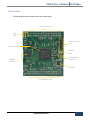
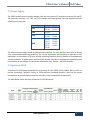
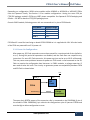
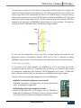
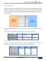
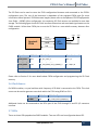
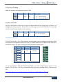
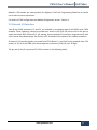
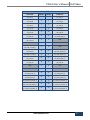
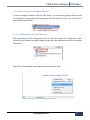
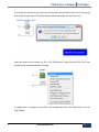
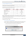
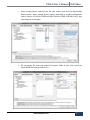
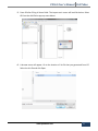
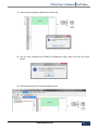
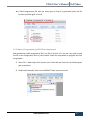
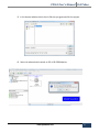
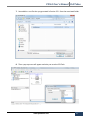
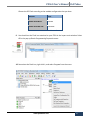
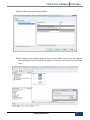
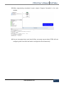
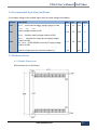
PXS61 Series User’s Manual
A compact (68mm x 63mm) FPGA board featuring
Xilinx Spartan-6 LX FPGA and on board LPDDR SDRAM
Copyright © 2012 PoliTekno Ltd.
PoliTekno Ltd.
Cyberpark Cyberplaza B Blok 2. Kat No:B225 Bilkent
06800 Ankara / TURKEY
+90 312 265 03 30
www.politekno.com
[email protected]
All rights reserved. Unauthorized duplication in whole or part of this document is prohibited without the
express written permission of PoliTekno Ltd.
PoliTekno and PoliTekno Logo are trademarks of PoliTekno Ltd. All other trademarks referenced herein are
the property of their respective owners and no trademark rights to the same are claimed.
Disclaimer
•
PoliTekno assumes no liability whatsoever for any direct, indirect, special, incidental, or
consequential damages arising from the use of this product.
•
While every effort has been made to ensure that the information provided on this manual is
accurate, PoliTekno assumes no liability or responsibility for any errors or omissions in the content
of this manual.
•
PoliTekno reserves the right to make changes and/or improvements to the products contained in
this manual without any notice.
Revision History:
Date
2012-04-24
Description
Initial release
Table of Contents
1 Introduction ................................................................................................................................... 4
1.1 Description ...................................................................................................................................................... 4
1.2 Features ........................................................................................................................................................... 5
1.3 Module Configurations .................................................................................................................................... 5
1.4 Overview.......................................................................................................................................................... 6
2 Functional Description.................................................................................................................... 7
2.1 Block Diagram .................................................................................................................................................. 7
2.2 Power Supply ................................................................................................................................................... 8
2.3 Spartan-6 FPGA................................................................................................................................................ 8
2.3.1 Power-On Configuration............................................................................................................................9
2.3.2 Power-On I/O State ................................................................................................................................ 10
2.4 LPDDR SDRAM ............................................................................................................................................... 11
2.5 SPI Flash ......................................................................................................................................................... 11
2.6 Clock Source .................................................................................................................................................. 12
2.7 LEDs ............................................................................................................................................................... 12
2.8 JTAG Connector ............................................................................................................................................. 13
2.9 External I/O Interface .................................................................................................................................... 14
3 Module Configuration .................................................................................................................. 17
3.1 JTAG Interface ............................................................................................................................................... 17
3.1.1 Generating an FPGA Configuration File .................................................................................................. 18
3.1.2 Configuring FPGA via JTAG interface ...................................................................................................... 18
3.2 Serial Configuration Interface ....................................................................................................................... 20
3.2.1 Generating a Flash Programming File .................................................................................................... 20
3.2.2 Indirect Programming of SPI Flash using Impact .................................................................................... 25
4 Technical Specifications ................................................................................................................ 32
4.1 Absolute Maximum Ratings........................................................................................................................... 32
4.2 Recommended Operating Conditions ........................................................................................................... 33
4.3 Mechanical Data ............................................................................................................................................ 33
4.3.1 Module Dimensions................................................................................................................................ 33
4.3.2 Top/Bottom Views.................................................................................................................................. 34
5 Support ........................................................................................................................................ 35
PXS61 User’s Manual PoliTekno
1 Introduction
1.1 Description
The PXS61 is a compact (68mm x 63mm, 2.67" x 2.48") FPGA board featuring the Xilinx Spartan-6 FPGA.
Designed as a full-featured integration system, the PXS61 module supports up to 128-MByte LPDDR
SDRAM and 128 Mbit SPI Flash. With over 60 I/O pins the PXS61 is designed to work with small to
medium-sized FPGA designs with a wide variety of external interface requirements.
The PXS61 has two standard 40-pin (2.54mm/100mil spaced) connectors on the bottom side. A
mechanical drawing of the PXS61 is shown at the end of this manual. Module connectors provide easy
access to many FPGA pins and dedicated module power supply pins. A simple base board which
generates necessary voltages for the module can be provided as an optional accessory for the PXS61
board.
www.politekno.com
4
PXS61 User’s Manual PoliTekno
1.2 Features
Xilinx Spartan-6 LX9/LX16/LX25 FPGAs up to 24,000 logic cells
6 pins header for FPGA configuration via JTAG
4/8/32/128 Mbit SPI Flash memory for FPGA configuration data (can be used also for storing user
data)
FPGA programming / debugging via JTAG connector
62 General Purpose I/O's (GPIO):
• Fit the standard 2.54mm / 0.1" headers allowing a wide range of additional functionality to
be added to the base board
• Available with and without soldered pitch pin headers
Done LED for identification of successful FPGA configuration
2 user LEDs for fast debugging
32 or 128 MByte DDR SDRAM:
• Up to 166 MHz clock frequency
• 16 bit data bus width
• MicroBlaze memory interface controller codes available
Temperature range: 0 to +70°C (commercial) or -40 to +85°C (industrial) versions available
1.3 Module Configurations
The following table shows part numbers and available module configurations. Custom configurations
are possible; please contact us for further information.
Ordering Code
FPGA
LPDDR SDRAM
SPI Flash
Temp. Range
PXS61-LX9-M0-F4
XC6SLX9-2FTG256C
-
4Mbit
0 to 70°C
PXS61-LX16-M0-F4
XC6SLX16-2FT256C
-
4Mbit
0 to 70°C
PXS61-LX25-M0-F8
XC6SLX25-2FT256I
-
8 Mbit
-40 to 85°C
PXS61-LX16-M32-F32
XC6SLX16-2FT256C
32 MByte
32 Mbit
0 to 70°C
PXS61-LX25-M128-F128
XC6SLX25-2FT256I
128 MByte
128 Mbit
-40 to 85°C
Each PXS61 series FPGA module is pin-to-pin compatible with each other. So increasing the FPGA
capacity or memory size is as easy as replacing the module with a higher capacity version without a
change needed in the base board design.
www.politekno.com
5
PXS61 User’s Manual PoliTekno
1.4 Overview
Following figure shows board layout and components.
I/O Connector (P2)
User
LEDs
JTAG Connector
(P3)
Spartan-6 FPGA
50 MHz
Clock
Configuration
Done LED
LPDDR
SDRAM
SPI Flash
I/O Connector (P1)
www.politekno.com
6
PXS61 User’s Manual PoliTekno
2 Functional Description
2.1 Block Diagram
External I/O Interface (P1)
32 GPIOs
LPDDR
SDRAM
(32/128 MByte)
JTAG Header
(P3)
up to
166 MHz
Xilinx
Spartan6 FPGA
(LX9/LX16/LX25)
SPI Flash Memory
(4/8/32/128 Mbit)
Clock
(50 MHz)
Done
LED
2 User
LEDs
30 GPIOs
External I/O Interface (P2)
www.politekno.com
7
PXS61 User’s Manual PoliTekno
2.2 Power Supply
The PXS61 module takes its supply voltages from the two external I/O interface connectors P1 and P2.
The internally required 1.2V, 1.8V, and 3.3V voltages and signal ground must be supplied from the
following connector pins:
Power Signals
1.2V
1.8V
3.3V
GND
Connector Pins
P1-19
P2-15
P1-38
P2-29
P1-18
P1-14
P2-16
P1-39
P2-28
P1-16
P2-14
P1-17
P2-18
P1-20
P2-27
P1-37
P2-30
P1-40
The external power supply should be sufficient and stabilized. For more details, please refer to Section
4 for recommended operating conditions. The current required on these supply pins depends on user
application i.e the number of I/O pins utilized, operating frequency and the number of simultaneously
switching outputs. So please use a tool like Xilinx XPower Estimator to estimate the expected power
consumption of your design. For details see Xilinx Power Tools Tutorial – UG733 from Xilinx.
2.3 Spartan-6 FPGA
A Spartan-6 LX FPGA (logic optimized) lies at the heart of every PXS61 series module. Built on a 45 nm
process technology, Spartan-6 family of FPGAs delivers expanded densities, with half the power
consumption of previous Spartan families, and faster, more comprehensive connectivity.
The table below shows summary of Spartan-6 LX FPGA features.
www.politekno.com
8
PXS61 User’s Manual PoliTekno
Depending on configuration, PXS61 series modules utilize XC6SLX9 or XC6SLX16 or XC6SLX25 FPGAs
from the Spartan-6 family. See Section 1.3 for module configurations. Having the same 256 pin
FT(G)256 package, module’s FPGAs are 100% pinout compatible. See Spartan-6 FPGA Packaging and
Pinouts – UG 385 for details of FT(G)256 package pinout.
On each PXS61 module, following power rails are connected to VCCO pins of FPGA banks:
FPGA Banks
Bank 0
Bank 1
Bank 2
Bank 3
Supply Voltage
3.3V
3.3V
3.3V
1.8V
FPGA Bank 3 is used for interfacing on board LPDDR SDRAM so it is supplied with 1.8V. All other banks
of the FPGA are powered from 3.3V power rail.
2.3.1 Power-On Configuration
After power-up, SPI Flash memories must not be accessed for a certain period of time (called tpu
or tpor). During this period all operations are disabled, and the flash does not respond to any
instruction. For some SPI Flash memories, this power-up time can be up-to 10-15 milliseconds.
This may cause some problems because at power-on FPGA sends a read command to the SPI
Flash to acquire the configuration data bitstream. In PXS61 modules, a voltage supervisor IC
was used to solve this issue. The circuitry to guarantee power-on compatibility between FPGA
and SPI Flash is shown below.
3.3V
VCCO_2
VCC
SPI
Flash
FPGA
PROGRAM_B
RESET#
Voltage
Supervisor
The open drain RESET# output of the supervisor chip is connected to the PROGRAM_B pin of
the module’s FPGA. PROGRAM_B pin controls the configuration cycle of Spartan-6 FPGAs and
must be High to allow configuration to start.
www.politekno.com
9
PXS61 User’s Manual PoliTekno
The supervisor IC monitors the 3.3V power rail and keeps its RESET# output Low as long as the
supply rail remains below the threshold value (3.15V). After this threshold value is reached, an
internal timer delays (120 milliseconds) the return of the RESET# output to the High state to
ensure proper system start-up. So the RESET# signal (and FPGA’s PROGRAM_B pin) is held Low
until power supply voltage reaches 3.15V + 120 ms reset delay time. After this point, RESET# is
released by the supervisor and PROGRAM_B goes to High via a pull-up resistor. The power-on
timing of the FPGA’s PROGRAM_B pin is illustrated in the figure below.
So, this way, the configuration cycle of the FPGA is delayed during every power-on and
guaranteed power-on compatibility between FPGA and SPI Flash is achieved by holding
PROGRAM_B pin Low until SPI Flash has powered up reliably and is ready to accept commands.
2.3.2 Power-On I/O State
In all versions of the PXS61 modules, the HSWAPEN pin (C4 on the FPGA) was directly
connected to GND via resistor R9. This enables pull-up resistors on all FPGA I/Os from poweron throughout configuration (See Spartan-6 FPGA Configuration User Guide – UG380 from
Xilinx). However a resistor (R21) was also added to set HSWAPEN pin to High if needed.
Therefore, there are two possible configurations for the HSWAPEN pin:
HSWAPEN Low (default Configuration via resistor R9)
HSWAPEN is grounded. This enables user I/O pull-up resistors from
power-on throughout configuration.
HSWAPEN High (alternative configuration via R21)
Remove R9 and solder R21 (a 0-Ω resistor). This way HSWAPEN is
pulled high. This disables the FPGA user I/O pull-up resistors allowing
FPGA I/Os to float from power-on throughout configuration.
www.politekno.com
10
PXS61 User’s Manual PoliTekno
2.4 LPDDR SDRAM
The PXS61 series modules are equipped with 32/128 MByte mobile low-power DDR SDRAM memory.
The memory device has an operating voltage of 1.8V and the interface is mobile DDR. Maximum clock
rate of the LPDDR SDRAM is 166 MHz and the interface signals are connected to I/O Bank 3 of the
FPGA. The following figure shows a high-level block diagram of the LPDDR Mobile SDRAM interface on
the PXS61 module.
Module’s SDRAM is attached exclusively to the FPGA and does not share any pins with the external I/O
connector.
The table below lists the LPDDR SDRAM memories available in PXS61 series modules:
Memory Type
Size
Configuration
Manufacturer
MT46H16M16LFBF-6 IT
32 MByte
(256 Mbit)
16M x 16bit
(4 Meg x 16 x 4 Banks)
Micron
MT46H64M16LFBF-6 IT
128 MByte
(1 Gbit)
64M x 16bit
(16 Meg x 16 x 4 Banks)
Micron
2.5 SPI Flash
Depending on configuration, PXS61 series modules contains 4/8/32/128 Mbit SPI Flash memory. The
table below shows the SPI Flash memories contained in PXS61 series FPGA modules.
Module
SPI Flash
Size
Manufacturer
Manufacturer
Part No.
PXS61-LX9-M0-F4
4Mbit
M25P40
Numonyx
PXS61-LX16-M0-F4
4Mbit
M25P40
Numonyx
PXS61-LX25-M0-F8
8 Mbit
M25P80
Numonyx
PXS61-LX16-M32-F32
32 Mbit
S25FL032P
Spansion
PXS61-LX25-M128-F128
128 Mbit
N25Q128
Numonyx
www.politekno.com
11
PXS61 User’s Manual PoliTekno
The SPI Flash can be used to store the FPGA configuration bitstream and connected to the FPGA’s
configuration port. The size of the bitstream is dependent of the equipped FPGA type (for more
information about Spartan-6 FPGA bitstream lengths please refer to the Spartan-6 FPGA Configuration
User Guide – UG380). After configuration, the remaining SPI Flash sectors are available for user data
storage. The following figure shows SPI Flash interface connections and associated signal names on the
PXS61 module. Utilize these FPGA pins to use the SPI Flash as a non-volatile memory element after
configuration.
3.3V
3.3V
CCLK
CSO_B
Spartan-6
FPGA
MOSI
WP#
SPI
Flash
HOLD#
DIN
Signal Name
FPGA Pin
FPGA Pin Type
Flash Pin Name*
FPGA_CCLK
R11
IO_L1P_CCLK_2
SCK / C
FPGA_CSO_B
T3
IO_L65N_CSO_B_2
CS# / S#
FPGA_MOSI
T10
IO_L3N_MOSI_CSI_B_MISO0_2
SI / DQ0 / D
FPGA_DIN
P10
IO_L3P_D0_DIN_MISO_MISO1_2
SO / DQ1 / Q
* Flash pin names differ depending on manufacturer
Please refer to Section 3 for more details about FPGA configuration and programming the SPI Flash
memory.
2.6 Clock Source
On PXS61 modules, a crystal oscillator with frequency of 50 MHz is connected to the FPGA. This clock
source can be used to generate new clocks within the FPGA using DCM's or PLL's.
Frequency
FPGA Pin
FPGA Pin Type
50 MHz
J16
IO_L43N_GCLK4_MQDQ5_1
Additional clocks can be connected to the GCLK pins of the FPGA through P1 and P2 I/O connector
interface.
2.7 LEDs
There are three LEDs populated on PXS61 modules. Two user LEDs and a configuration done LED.
www.politekno.com
12
PXS61 User’s Manual PoliTekno
Configuration LED: DONE
DONE LED Indicates the configuration state of FPGA.
LED
Reference Color
DONE D4
Green
FPGA Pin
Description
P13
Configuration Done LED
on – FPGA configured
off – FPGA not configured
User LEDs: LED1, LED2
Two user LEDs (LED1 & LED2) can be used to indicate status of the internal logic in FPGA or for
debugging and similar purposes. These LEDs are lit by driving the associated FPGA I/O pin to logic high
and are off when the pin is either low or not driven.
LED
Reference Color
FPGA Pin
Description
LED1
D2
Yellow
A4
User LED - Active high
LED2
D3
Yellow
D5
User LED - Active high
2.8 JTAG Connector
P3 is the 2.54 mm/0.1", 6-pin JTAG connector on board and is used to configure the Spartan-6 FPGA
and program the configuration device (SPI Flash). The PXS61 module has one device in the JTAG chain,
the Spartan-6 FPGA. The JTAG connector pins are connected as shown below.
Pin Signal FPGA
Direction
No. Name Pin
Description
1
TMS
A15
IN
JTAG TMS
2
TDI
C12
IN
JTAG TDI
3
TDO
E14
OUT
JTAG TDO
4
TCK
C14
IN
JTAG TCK
5
GND
-
POWER
Signal ground
6
VCC
-
POWER
3.3V
Please pay attention not to attach cables in reverse
You can use Digilent’s JTAG HS1 Programming Cable or a similar programmer to connect to the
module’s JTAG interface. JTAG HS1 is compatible with all Xilinx tools, including iMPACT, Chipscope, and
EDK.
http://www.digilentinc.com/Products/Detail.cfm?NavPath=2,395,922&Prod=JTAG-HS1
www.politekno.com
13
PXS61 User’s Manual PoliTekno
Module’s JTAG header pin order perfectly fits Digilent’s JTAG HS1 Programming Cable but be careful
not to make a reverse connection.
For details of JTAG configuration see Module Configuration section - Section 3.
2.9 External I/O Interface
Two 40 pin (2x20) connectors, P1 and P2, are available on the bottom-side of the PXS61 series FPGA
modules. These expansion connectors provide user access to 62 FPGA I/O pins as well as the pins to
supply the board. With 2.54mm/0.1" pin spacing, these standard I/O connectors integrates easily with
user’s custom base board design. See Section 4.3.1 for details of the layout of the module connectors.
All external I/O interface signals are routed from FPGA Banks 0, 1 and 2 which are powered from 3.3V
power rail. So, all of the FPGA I/O at these expansion connectors (P1 & P2) are 3.3V logic.
The pin-out of the I/O connectors P1 & P2 are shown in the following tables:
www.politekno.com
14
PXS61 User’s Manual PoliTekno
Pin List (P1)
Pin No. Pin No.
FPGA Pin
T4
(IO_L63N_2)
R5
(IO_L48P_D7_2)
T5
(IO_L48N_RDWR_B_VREF_2)
T6
(IO_L47N_2)
FPGA Pin
P4
(IO_L63P_2)
N5
(IO_L49P_D3_2)
P5
(IO_L49N_D4_2)
P6
(IO_L47P_2)
1
2
3
4
5
6
7
8
R7
(IO_L32P_GCLK29_2)
9
10
N6
(IO_L64N_D9_2)
T7
(IO_L32N_GCLK28_2)
11
12
P7
(IO_L31P_GCLK31_D14_2)
13
14
3V3
15
16
GND
GND
17
18
1V8
1V2
19
20
GND
P9
(IO_L14N_D12_2)
21
22
T8
(IO_L30N_GCLK0_USERCCLK_2)
T9
(IO_L23N_2)
23
24
R9
(IO_L23P_2)
25
26
27
28
29
30
31
32
R16
(IO_L49N_M1DQ11_1)
33
34
P15
(IO_L48P_HDC_M1DQ8_1)
P16
(IO_L48N_M1DQ9_1)
35
36
N16
(IO_L45N_A0_M1LDQSN_1)
GND
37
38
1V2
3V3
39
40
GND
P8
(IO_L30P_GCLK1_D13_2)
N8
(IO_L29N_GCLK2_2)
T12
(IO_L52N_M1_DQ15_1)
T13
(IO_L51N_M1DQ13_1)
M9
(IO_L29P_GCLK3_2)
T15
(IO_L50N_M1UDQSN_1)
www.politekno.com
R12
(IO_L52P_M1DQ14_1)
T14
(IO_L51P_M1DQ12_1)
R14
(IO_L50P_M1UDQS_1)
R15
(IO_L49P_M1DQ10_1)
15
PXS61 User’s Manual PoliTekno
Pin List (P2)
Pin No. Pin No.
FPGA Pin
B5
(IO_L2P_0)
A5
(IO_L2N_0)
B6
(IO_L4P_0)
A6
(IO_L4N_0)
FPGA Pin
C5
(IO_L3N_0)
D6
IO_L7P_0()
C6
(IO_L7N_0)
C7
(IO_L6P_0)
1
2
3
4
5
6
7
8
A7
(IO_L6N_0)
9
10
D8
(IO_L38P_0)
B8
(IO_L33P_0)
11
12
C8
(IO_L38N_VREF_0)
A8
(IO_L33N_0)
13
14
GND
1V2
15
16
3V3
17
18
GND
19
20
C9
(IO_L34P_GCLK19_0)
A10
(IO_L35N_GCLK16_0)
21
22
B10
(IO_L35P_GCLK17_0)
A11
(IO_L39N_0)
23
24
A12
(IO_L62N_VREF_0)
C11
(IO_L39P_0)
25
26
B12
(IO_L62P_0)
GND
27
28
3V3
1V2
29
30
GND
A14
(IO_L65N_SCP2_0)
31
32
A13
(IO_L63N_SCP6_0)
B14
(IO_L65P_SCP3_0)
33
34
C10
(IO_L37N_GCLK12_0)
B16
(IO_L29N_A22_M1A14_1)
35
36
B15
(IO_L29P_A23_M1A13_1)
37
38
39
40
A9
(IO_L34N_GCLK18_0)
D9
(IO_L40N_0)
C16
(IO_L33N_A14_M1A4_1)
E16
(IO_L34N_A12_M1BA2_1)
www.politekno.com
C15
(IO_L33P_A15_M1A10_1)
D16
(IO_L31N_A18_M1A12_1)
16
PXS61 User’s Manual PoliTekno
3 Module Configuration
3.1 JTAG Interface
The FPGA devices on PXS61 series modules can be configured using the JTAG interface through header
P3. Configuring FPGA directly from JTAG interface is volatile i.e. FPGA loses its configuration after reset or
power cycle.
Regardless of the configuration mode settings, the JTAG interface is available as a configuration
interface any time the device is powered. JTAG interface can also be used for debugging Microblaze
projects and viewing internal signals through ChipScope.
www.politekno.com
17
PXS61 User’s Manual PoliTekno
3.1.1 Generating an FPGA Configuration File
In order to configure module’s FPGA via JTAG directly, you should first generate the bit stream
file (.bit file) by running Generate Programming File from Xilinx ISE. This is the final step in a
typical FPGA synthesis flow.
3.1.2 Configuring FPGA via JTAG interface
After generating an FPGA configuration file from ISE open Impact for configuration. While
connected to the module through a programming cable, select Boundary-Scan from the Impact
Flows menu.
Right click in the Boundary Scan window and select Initialize Chain.
www.politekno.com
18
PXS61 User’s Manual PoliTekno
At this step you should see your device in the Boundary Scan window. Select Yes in the pop-up
Auto Assign Configuration Files Query Dialog window and assign your bit-stream file.
Select No when asked to attach an SPI or BPI PROM device. Right-click the FPGA icon in the
Boundary Scan window and select Program.
If configuration is completed successfully, the configuration done LED should light up on the
PXS61 board.
www.politekno.com
19
PXS61 User’s Manual PoliTekno
3.2 Serial Configuration Interface
The SPI Flash can be used to store the FPGA configuration bitstream. This way, FPGA can read and
configure itself at every power-up from the SPI Flash.
Spartan-6 devices use two pins M1 and M0, which define the configuration modes. See the table below
for different configuration modes of Spartan-6 devices.
M[1:0] is configured as Master Serial mode (M[1:0] = 01) in PXS61 series modules. In master serial
configuration mode, FPGA reads the bitstream from the SPI Flash (by loading one configuration bit per
configuration clock cycle) during every power-up.
For more information about the master serial configuration please refer to the Spartan-6 FPGA
Configuration User Guide – UG380.
3.2.1 Generating a Flash Programming File
In order to program the configuration flash you should first generate a flash programming file
(.mcs file). Follow the steps below for generating flash programming file for your project.
1. Generate FPGA bitstream file (.bit file) from your FPGA project in ISE.
2. Open Impact. Select Yes from the pop-up menu below.
www.politekno.com
20
PXS61 User’s Manual PoliTekno
3. Select Prepare a PROM File from the menu below.
4. From the PROM File formatter menu
• Select Configure Single FPGA submenu under SPI Flash storage device type and click
the green arrow.
www.politekno.com
21
PXS61 User’s Manual PoliTekno
•
Select storage device capacity from the next column and click the Add Storage
Device button. Select storage device capacity according to module configuration
table in Section 1.3 (4M for PXS61-LX9-M0-F4, 8M for PXS61-LX25-M0-F8 etc.) then
click the green arrow again.
•
Fill the output file name and output file location fields as your wish. Leave the
Flash/PROM File Property fields as it is.
www.politekno.com
22
PXS61 User’s Manual PoliTekno
5. Press OK after filling all these fields. The impact main menu will look like below. Select
OK from the Add Device pop-up menu below.
6. A browse menu will appear. Go to the location of .bit file that you generated from ISE.
Select the .bit file and click Open.
www.politekno.com
23
PXS61 User’s Manual PoliTekno
7. Select No when asked to add another device file.
8. You are now completed the PROM file preparation steps. Select OK from the menu
below.
9. Now select Generate File from Operations menu.
www.politekno.com
24
PXS61 User’s Manual PoliTekno
10. A Flash programming file with the name given in Step 4 is generated under the file
location specified again in Step 4.
3.2.2 Indirect Programming of SPI Flash using Impact
After generating a flash programming file (.mcs file) in Section 3.2.1 you are now ready to load
this file to the configuration flash in your module. Follow the steps below to program the flash
using Impact.
1. Select File -> New Project from Impact menu. Select No and Cancel for the following two
pop-up windows.
2. Double click Boundary Scan from the iMPACT Flows menu on the left.
www.politekno.com
25
PXS61 User’s Manual PoliTekno
3. Right click and select Initialize Chain from the Boundary Scan window.
4. If JTAG signals are OK, Impact will show the components connected to the JTAG chain in
your board. Select Yes when asked to assign configuration files from the pop-up menu
below:
www.politekno.com
26
PXS61 User’s Manual PoliTekno
5. In the browse window select the .bit file that you generated for the project.
6. Select Yes when asked to attach an SPI or BPI PROM device.
www.politekno.com
27
PXS61 User’s Manual PoliTekno
7. Now add the .mcs file that you generated in Section 3.2.1 from the associated folder.
8. Then a pop-up menu will appear and asks you to select SPI Flash.
www.politekno.com
28
PXS61 User’s Manual PoliTekno
Choose the SPI Flash according to the module configuration that you have.
Module
Flash
PXS61-LX9-M0-F4
M25P40
PXS61-LX16-M0-F4
M25P40
PXS61-LX25-M0-F8
M25P80
PXS61-LX16-M32-F32
S25FL032P
PXS61-LX25-M128-F128
N25Q128 1.8/3.3V
9. You should see the Flash icon attached to your FPGA in the Impact main window. Select
OK in the pop-up Device Programming Properties menu.
10. Now select the flash icon, right click it, and select Program from the menu.
www.politekno.com
29
PXS61 User’s Manual PoliTekno
11. Select OK from the pop-up menu below:
12. The program starts programming the Flash on the module. You can see the progress
from the Impact Console window. Depending on Flash size this process may take some
time.
www.politekno.com
30
PXS61 User’s Manual PoliTekno
13. When programming completed, Impact outputs Program Succeeded in the main
window.
14. You can now power down your board. When you power-up your board, FPGA will start
configuring itself from flash and loads its configuration file automatically.
www.politekno.com
31
PXS61 User’s Manual PoliTekno
4 Technical Specifications
4.1 Absolute Maximum Ratings
Symbol
1V2
3V3
Description
VCCINT - FPGA Internal supply voltage relative to GND
VCCO_0 / VCCO_1 / VCCO_2 - FPGA Bank 0/1/2 Output drivers
supply voltage relative to GND
Rating
–0.5 to 1.32
Units
V
–0.5 to 3.75
V
-0.3 to 2.7
V
VCCAUX - Auxiliary supply voltage relative to GND
VCCO_3 - FPGA Bank 3 Output drivers supply voltage
relative to GND
1V8
Temp
VDD / VDDQ - LPDDR SDRAM core and I/O supply voltage
relative to GND
Ambient temperature for commercial modules (C)
0 to +70
°C
Ambient temperature for industrial modules (I)
www.politekno.com
-40 to +85
32
PXS61 User’s Manual PoliTekno
4.2 Recommended Operating Conditions
Do not apply voltage to the module higher than the rated voltages listed below.
Symbol
Description
Min.
Typ.
Max.
Units
1V2
VCCINT - FPGA Internal supply voltage relative to GND
VCCO_0 / VCCO_1 / VCCO_2 - FPGA Bank 0/1/2 Output drivers
supply voltage relative to GND
1.14
1.2
1.26
V
3.15
3.3
3.45
V
1.7
1.8
1.95
V
0
-40
-
+70
+85
°C
3V3
1V8
Temp
VCCAUX - Auxiliary supply voltage relative to GND
VCCO_3 - FPGA Bank 3 Output drivers supply voltage
relative to GND
VDD / VDDQ - LPDDR SDRAM core and I/O supply voltage
relative to GND
Ambient temperature for commercial modules (C)
Ambient temperature for industrial modules (I)
4.3 Mechanical Data
4.3.1 Module Dimensions
All dimensions are in millimeters.
www.politekno.com
33
PXS61 User’s Manual PoliTekno
4.3.2 Top/Bottom Views
www.politekno.com
34
PXS61 User’s Manual PoliTekno
5 Support
If you need more information, have any problem with your PXS61 module or have found an error in
this document please contact us.
PoliTekno Ltd.
Cyberpark Cyberplaza B Blok 2. Kat No:B225 Bilkent
06800 Ankara / TURKEY
+90 312 265 03 30
www.politekno.com
[email protected]
www.politekno.com
35