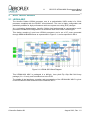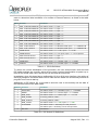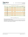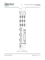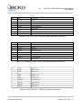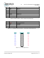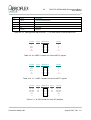
1
GR-CPCI-LEON4-N2X
Development Board
User Manual
AEROFLEX GAISLER AB
Rev. 1.2, 2013-08-27
2
GR-CPCI-LEON4-N2X Development Board
User Manual
Information furnished by Aeroflex Gaisler AB is believed to be accurate and reliable.
However, no responsibility is assumed by Aeroflex Gaisler AB for its use, nor for any infringements
of patents or other rights of third parties which may result from its use.
No license is granted by implication or otherwise under any patent or patent rights of Aeroflex
Gaisler AB.
Aeroflex Gaisler AB
tel +46 31 7758650
Kungsgatan 12
fax +46 31 421407
411 19 Göteborg
[email protected]
Sweden
www.aeroflex.com/gaisler
Copyright © 2013 Aeroflex Gaisler
All information is provided as is. There is no warranty that it is correct or suitable for any purpose,
neither implicit nor explicit.
© Aeroflex Gaisler AB
August 2013, Rev. 1.2
3
GR-CPCI-LEON4-N2X Development Board
User Manual
TABLE OF CONTENTS
1
INTRODUCTION.........................................................................................................7
1.1
1.2
1.3
1.4
2
Overview................................................................................................................... 7
References................................................................................................................9
Handling.................................................................................................................... 9
Abbreviations........................................................................................................... 10
ELECTRICAL DESIGN.............................................................................................11
2.1
2.2
2.3
2.4
2.4.1
2.4.2
2.4.3
2.5
2.5.1
2.5.2
2.5.3
2.5.4
2.6
2.7
2.7.1
2.7.2
2.8
2.9
2.10
2.11
2.12
2.13
2.14
2.15
2.16
2.16.1
2.16.2
2.16.3
2.16.4
2.16.5
2.16.6
2.16.7
2.17
2.18
LEON4 ASIC........................................................................................................... 11
Board Block Diagram..............................................................................................12
Board Mechanical Configuration..............................................................................13
Memory................................................................................................................... 14
DDR2 RAM.............................................................................................................. 14
PC-100 SDRAM......................................................................................................14
Parallel FLASH........................................................................................................15
PCI Interface........................................................................................................... 16
Host/System Slot Configuration...............................................................................16
Peripheral Slot Configuration...................................................................................17
PCI Reset Circuits...................................................................................................18
33 / 66 MHz PCI Bus Speed....................................................................................18
Ethernet Interface....................................................................................................18
Spacewire (LVDS) Interfaces..................................................................................19
SPW interface circuit...............................................................................................19
SPW Connectors.....................................................................................................20
USB Debug Communication Link............................................................................20
Serial Interface (RS232)..........................................................................................21
FTDI Serial to USB Interface...................................................................................21
MIL-STD-1553 Interface.........................................................................................22
SPI interface............................................................................................................ 23
GPIO....................................................................................................................... 24
Memory Expansion..................................................................................................25
Debug Support Unit Interfaces................................................................................26
Other Auxiliary Interfaces and Circuits....................................................................27
Oscillators and Clock Inputs....................................................................................27
Power Supply and Voltage Regulation....................................................................29
Reset Circuit and Button..........................................................................................32
Watchdog................................................................................................................ 32
JTAG interface........................................................................................................ 32
eASIC JTAG Interface.............................................................................................32
Heatsink/Fan........................................................................................................... 33
Technology Table / Routing Rules...........................................................................34
Layer Stack-up........................................................................................................ 36
3
SETTING UP AND USING THE BOARD.................................................................38
4
INTERFACES AND CONFIGURATION....................................................................40
4.1
4.2
4.3
List of Connectors...................................................................................................40
List of Oscillators, Switches and LED's...................................................................50
List of Jumpers........................................................................................................52
© Aeroflex Gaisler AB
August 2013, Rev. 1.2
4
GR-CPCI-LEON4-N2X Development Board
User Manual
LIST OF TABLES
Table 2-1: GPIO Definitions.......................................................................................................... 25
Table 2-2: DIP Switch S3 Definitions.............................................................................................25
Table 2-3: Vcore Voltage Adjustment Settings...............................................................................30
Table 2-4: Technology Table /Routing Rules Summary.................................................................36
Table 3-1: Default Status of Jumpers/Switches..............................................................................38
Table 4-1: List of Connectors......................................................................................................... 40
Table 4-2: J1A (Top) RJ45 10/100/1000 Mbit/s Ethernet Connector 1.........................................43
Table 4-3: J1B (Bottom) RJ45 10/100/1000 Mbit/s Ethernet Connector 0....................................43
Table 4-4: J2A SPW-DCL – SPW-DCL interface connections .....................................................43
Table 4-5: J2B-J2I SPW-0 – SPW-7 interface connections (8x)...................................................44
Table 4-6: J3 USB type Mini AB connector – USB Debug Communication Link...........................44
Table 4-7: J4 PIO Header Pin out..................................................................................................44
Table 4-8: J5 USB type Mini AB connector – FTDI Dual Serial Communication Link....................45
Table 4-9: J6 -UART-0 Header for Serial UART 0 signals.............................................................45
Table 4-10: J7 – UART-1 Header for Serial UART 1 signals..........................................................45
Table 4-11: J8- SPI Header for User SPI interface........................................................................45
Table 4-12: Expansion connector J9 Pin-out..................................................................................46
Table 4-13: J10 USER– JTAG Connector .....................................................................................47
Table 4-14: J11 ASIC – JTAG Connector .....................................................................................47
Table 4-15: J12 POWER – External Power Connector..................................................................47
Table 4-16: J13 POWER – External Power Connector..................................................................48
Table 4-17: J14 – Dual MIL-STD-1553 Interface signals................................................................48
Table 4-18: J15 DDR2 SODIMM - 200 pin socket for DDR2 SODIMM.........................................49
Table 4-19: J16 DDR2 SODIMM - 200 pin socket for DDR2 SODIMM.........................................50
Table 4-20: List and definition of Oscillators and Crystals..............................................................51
Table 4-21: List and definition of PCB mounted LED's...................................................................51
Table 4-22: List and definition of Switches.....................................................................................51
Table 4-23: DIP Switch S1 'PIO[7..0]' definition.............................................................................52
Table 4-24: DIP Switch S2 'PIO[15..8]' definition............................................................................52
Table 4-25: DIP Switch S3 definition..............................................................................................52
Table 4-26: List and definition of PCB Jumpers.............................................................................53
LIST OF FIGURES
Figure 1-1: GR-CPCI-LEON4-N2X Development Board..................................................................7
Figure 2-1: LEON4 SOC Block Diagram........................................................................................11
Figure 2-2: LEON4-N2X-ASIC-DEMO............................................................................................12
Figure 2-3: Block Diagram of GR-CPCI-LEON4-N2X board..........................................................12
Figure 2-4: GR-CPCI-LEON4-N2X Board with CPCI Front Panel .................................................13
Figure 2-5: Block diagram for PCI System Slot connections..........................................................16
Figure 2-6: Block diagram of PCI Peripheral connections..............................................................17
Figure 2-7: Block diagram of Ethernet GMII/MII Interface .............................................................19
Figure 2-8: SPW flex connection....................................................................................................20
Figure 2-9: USB Host Controller PHYsical Interface......................................................................21
Figure 2-10: Serial interface........................................................................................................... 21
Figure 2-11: Block diagram of FTDI Serial/JTAG to USB Interface...............................................22
Figure 2-12: MIL-STD-1553 Transceiver and Transformer circuit .................................................23
Figure 2-13: Ribbon cable connection to front Panel D-SUB connectors.......................................23
© Aeroflex Gaisler AB
August 2013, Rev. 1.2
5
GR-CPCI-LEON4-N2X Development Board
User Manual
Figure 2-14: SPI Interface Configuration........................................................................................24
Figure 2-15: PIO interface.............................................................................................................. 24
Figure 2-16: Debug Support Unit connections................................................................................27
Figure 2-17: Board level Clock Distribution Scheme......................................................................28
Figure 2-18: Power Regulation Scheme.........................................................................................31
Figure 2-19: Watchdog configuration.............................................................................................32
Figure 2-20: Layer Stack-up (TBC)................................................................................................37
Figure 4-1: Front Panel View .........................................................................................................41
Figure 4-2: PCB Top View.............................................................................................................. 53
Figure 4-3: PCB Bottom View.........................................................................................................54
Figure 4-4: PCB Top View (Photo).................................................................................................55
Figure 4-5: PCB Bottom View (Photo)............................................................................................56
REVISION HISTORY
Revision
Date
0.0 DRAFT
Page
Description
All
Draft
Table 4-12
Pin READ removed from connector J9
1.0
2013-04-09 All
Updated text to match 'as-built' hardware description, with rev 1.1
hardware, and made various corrections.
1.1
2013-08-27 All
Various corrections and updates after review.
1.2
2013-08-27 2-4, 2-8,2-13 Updated figures.
Table 3-1.
Corrected for JP11.
§1.2, §2.14
Added note about expansion connector pin numbering and added a link to
reference document about Mezzanine Connectors
§2.16.2
Modified text description of Vcore adjustment
© Aeroflex Gaisler AB
August 2013, Rev. 1.2
6
GR-CPCI-LEON4-N2X Development Board
User Manual
Intentionally Blank
© Aeroflex Gaisler AB
August 2013, Rev. 1.2
7
1
GR-CPCI-LEON4-N2X Development Board
User Manual
INTRODUCTION
1.1 Overview
This document describes the GR-CPCI-LEON4-N2X Development Board.
The purpose of this equipment is to provide developers with a convenient hardware platform
for the evaluation and development of software for the Aeroflex Gaisler LEON4-N2X
Processor for the LEON4FT-NGMP project.
The LEON4 processor is a 32-bit processor compliant to the SPARC V8 architecture. In this
variant, Aeroflex Gaisler has implemented a Multi-Core LEON4FT processor with a rich set
of IP cores and interfaces in a eASIC Nextreme2 structured ASIC.
The GR-CPCI-LEON4-N2X Development Board comprises a custom designed PCB in a 6U
Compact PCI format, making the board suitable for stand-alone bench top development, or if
required, to be mounted in a 6U CPCI Rack.
The principle interfaces and functions are accessible on the front and back edges of the
board, and secondary interfaces via headers on the board.
Figure 1-1: GR-CPCI-LEON4-N2X Development Board
© Aeroflex Gaisler AB
August 2013, Rev. 1.2
8
GR-CPCI-LEON4-N2X Development Board
User Manual
The board contains the following main items as detailed in section 2 of this document:
•
LEON4-N2X ASIC with Multi-Core Leon4FT architecture
•
CPCI Interface
•
Memory
• DDR2-600 SDRAM
• PC-100 SDRAM
• Parallel Boot FLASH
1 slot 96 bits wide, DDR2-SODIMM
1 bank 96 bits wide, Discrete chips
64 Mbit (16bit wide x 4M or 8bit wide x 8M)
•
Power, Reset, Clock and Auxiliary circuits
•
Interface circuits required for the features listed below
The interface connectors on the Front edge of the board provide:
•
Dual RJ45 10/100/1000 Mbit GMII/MII Ethernet interface (KSZ9021GN with RJ45 jack)
•
8 port SPW interface (8 x MDM9S)
•
SPW Debug Comm. Link (MDM9S)
•
USB2.0 Debug Comm. Link Interface (ISP1504A with USB-Mini-AB)
•
16 bit General Purpose I/O (34 pin 0.1” ribbon cable style connector)
•
FTDI Serial to USB interface (FT2232HL with USB-Mini-AB)
The interface connectors on the Back edge of the board provide:
• Compact PCI interface (32 bit, 33/66MHz), configurable for Host or Peripheral slot
•
Input power connector (+5V nom.)
To enable convenient connection to the interfaces, most connector types and pin-outs are
compatible with the standard connector types for these types of interfaces.
Additionally, on-board headers and components provide access to the following functions/
features:
• Dual MIL-1553 Interface (can be connected to front panel with short ribbon cable
connection to a D-sub 9 Male connector)
• DIP switches for GPIO signal configuration
• DIP Switch for Memory interface configuration
• LED indicators connected to GPIO signals
• SPI interface user connections on 0.1” header
• Two Serial UART (RS232) interfaces (can be connected to front panel with short
ribbon cable connection with D-sub 9 female connectors)
• JTAG Debug interface
• Test connector for access to eASIC JTAG interface
• 4 pin Molex style power connector
• Push Buttons for RESET and DSU-BREAK
• LED indicators for POWER, ERRORN, DSU Active and GPIO
• Assorted jumpers and Test Points for configuration and Test of the board
© Aeroflex Gaisler AB
August 2013, Rev. 1.2
9
GR-CPCI-LEON4-N2X Development Board
User Manual
Debug interface support is demonstrated on the board with support for debugging via the
following interfaces:
•
•
•
•
JTAG
ETH (EDCL)
USB (USB-DCL)
SPW (SPW-DCL)
Please note that the LEON4-N2X device has errata that affects interfaces such as the PCI
interface. Please refer to the errata section of RD-4.
1.2 References
RD-1 GR-CPCI-LEON4-N2X_schematic.pdf, Schematic (included on CD)
RD-2 GR-CPCI-LEON4-N2X_assy_drawing.pdf, Assembly Drawing (included on CD)
RD-3 GR-CPCI-LEON4-N2X_bom.pdf, Bill of Materials (included in CD)
RD-4 LEON4-N2X Data Sheet and User’s Manual, Aeroflex Gaisler, latest version is
available via http://www.gaisler.com/gr-cpci-leon4-n2x
RD-5 GRMON2 User Manual, Aeroflex Gaisler, part of GRMON2 package.
RD-6 GR-MEZZ Technical Note, Technical Note about Mezzanine connectors
1.3 Handling
ATTENTION : OBSERVE PRECAUTIONS FOR
HANDLING ELECTROSTATIC SENSITIVE DEVICES
This unit contains sensitive electronic components which can be damaged by Electrostatic
Discharges (ESD). When handling or installing the unit observe appropriate precautions and
ESD safe practices.
When not in use, store the unit in an electrostatic protective container or bag.
When configuring the jumpers on the board, or connecting/disconnecting cables, ensure that
the unit is in an un-powered state.
When operating the board in a 'stand-alone' configuration, the power supply should be
current limited to prevent damage to the board or power supply in the event of an overcurrent situation.
This board is intended for commercial use and evaluation in a standard laboratory
environment, nominally, 20°C. All devices are standard commercial types, intended for use
over the standard commercial operating temperature range (0 to 70ºC).
© Aeroflex Gaisler AB
August 2013, Rev. 1.2
10
GR-CPCI-LEON4-N2X Development Board
User Manual
1.4 Abbreviations
ASIC
CPCI
DIL
DDR
DSU
ESD
GPIO
I/O
IP
MII
MUX
PCB
GMII
SOC
SPW
TBC
Application Specific Integrated Circuit.
Compact Peripheral Connect Interface
Dual In-Line
Double Data Rate
Debug Support Unit
Electro-Static Discharge
General Purpose Input / Output
Input/Output
Intellectual Property
Media Independent Interface
Multiplexer
Printed Circuit Board
Gigibit Media Independent Interface
System On a Chip
Spacewire
To be Confirmed
© Aeroflex Gaisler AB
August 2013, Rev. 1.2
11
2
GR-CPCI-LEON4-N2X Development Board
User Manual
ELECTRICAL DESIGN
2.1 LEON4 ASIC
The Aeroflex Gaisler LEON4 processor core is a synthesizable VHDL model of a 32-bit
processor compliant with the SPARC V8 architecture. The core is highly configurable and
particularly suitable for high performance multi-core system-on-a-chip (SOC) designs.
As a technology demonstrator, Aeroflex Gaisler has implemented a representative mulitprocessor LEON4-N2X configuration in a Structured ASIC from eASIC technologies.
This design consists of quad core LEON4 processors and a set of IP cores connected
through AMBA AHB/APB buses as represented in Figure 2-1, and as specified in RD-4.
Figure 2-1: LEON4 SOC Block Diagram
This LEON4-N2X ASIC is packaged in a 896-pin, 1mm pitch Flip Chip Ball Grid Array
package (31 x 31 mm), and is soldered on to the PCB.
The details of the interfaces, operation and programming of the LEON4-N2X ASIC is given
in the LEON4-N2X Data Sheet and User’s Manual, RD-4.
© Aeroflex Gaisler AB
August 2013, Rev. 1.2
12
GR-CPCI-LEON4-N2X Development Board
User Manual
Figure 2-2: LEON4-N2X-ASIC-DEMO
2.2 Board Block Diagram
The GR-CPCI-LEON4-N2X Board provides the electrical functions and interfaces as
represented in the block diagram, Figure 2-3.
DDR2
DDR2
RAM
RAM
PC100
PC100
SDRAM
SDRAM
LEON4
ASIC
PARALLEL
PARALLEL
FLASH
FLASH
POWER
POWER IN
IN
POWER
POWER AND
AND
REGULATION
REGULATION
CPCI
CPCI
88 xx SPW
SPW I/F
I/F
SPW
SPW
DUAL
DUAL 10/100/1000
10/100/1000 ETHERNET
ETHERNET
ETHERNET
ETHERNET
USB-DCL
USB-DCL
USB-DCL
USB-DCL
SPW-DCL
SPW-DCL
SPW-DCL
SPW-DCL
USER
USER I2C
I2C I/F
I/F
I2C
I2C I/F
I/F
USER
USER I/O
I/O
USER
USER I/O
I/O
22 xx MIL-1553
MIL-1553 I/F
I/F
1553
1553 I/F
I/F
JTAG-DEBUG
JTAG-DEBUG
JTAG
JTAG I/F
I/F
22 xx SERIAL
SERIAL UART
UART I/F
I/F
RS232
RS232
FTDI
FTDI SERIAL
SERIAL TO
TO USB
USB I/F
I/F
FTDI-USB
FTDI-USB
COMPACT
COMPACT
PCI
PCI I/F
I/F
Figure 2-3: Block Diagram of GR-CPCI-LEON4-N2X board
© Aeroflex Gaisler AB
August 2013, Rev. 1.2
13
GR-CPCI-LEON4-N2X Development Board
User Manual
2.3 Board Mechanical Configuration
The Main PCB is a 6U Compact PCI format board (233.5 x 160mm) and can be used 'standalone' on the bench-top simply using an external +5V power supply, or can be plugged in to
a Compact PCI backplane.
Figure 1-1, shows the board as a stand alone PCB. However, for installation into a Compact
PCI rack, this board is provided with a custom CPCI front panel with the with the appropriate
connector cut-outs. The front panel concept is shown in Figure 2-4, with MDM9S style
connectors for the Spacewire interfaces.
Figure 2-4: GR-CPCI-LEON4-N2X Board with CPCI Front Panel
© Aeroflex Gaisler AB
August 2013, Rev. 1.2
14
GR-CPCI-LEON4-N2X Development Board
User Manual
2.4 Memory
The memory configuration installed on the board comprises:
•
SODIMM socket for SODIMM mounted DDR2 RAM (1 or 2 Gbyte modules)
•
Discrete PC-100 SDRAM chips providing 96 bit wide interface (6 x 256Mbit)
•
128 Mbit of Flash PROM, in Parallel 8 bit flash device
Note that, although both DDR2 and SDRAM are provided on the board, only one or the
other can be used at one time. This is determined by the state of the mem_ifsel pin at
power on of the board.
2.4.1 DDR2 RAM
The LEON4-N2X ASIC incorporates a 96 bit wide DDR2 RAM Data interface (64 bits data
plus 32 bits EDAC check bits).
To accommodate this in a flexible way, two 204 pin DDR2 SODIMM sockets are
implemented on board, one socket for the 64 bits data and the second socket (Half used) for
the 32 bits EDAC check bit data paths.
Due to the size and configuration of the SODIMM sockets, one socket is mounted on the top
side and the other socket on the bottom side of the board, in a 'mirror image' as represented
in the figure below.
Note that the height of the SODIMM socket on the bottom side of the
board is approximately 5.2mm. Strictly speaking, the CPCI specification
only allows an envelope of 2.54mm for the component heights on the
bottom side of the board, and the board is therefore not fully compliant.
This is unlikely to cause an actual problem in use, since the volume
required by the bottom side socket is most likely to be 'free air' in any
normal single or dual slot board mounted in the adjacent slot. However, it will be necessary
to take care when installing and removing the card from a PCI rack. Do not simply yank the
card out of the rack since this bottom side SODIMM socket will make contact against the
front panel of the adjacent card when you try to slide it out of the rack, and this may damage
the board. YOU MUST NOT TRY TO USE FORCE TO REMOVE THE CARD! Instead the
adjacent card will have to be loosened or removed first in order to allow the GR-CPCILEON4-N2X card to be removed.
2.4.2 PC-100 SDRAM
The LEON4-N2X ASIC incorporates a 96 bit wide PC-100 SDRAM Data interface (64 bits
data plus 32 bits EDAC check bits).
To accommodate this, six 256Mbit Micron MT48LC16M16 devices are soldered on to the
© Aeroflex Gaisler AB
August 2013, Rev. 1.2
15
GR-CPCI-LEON4-N2X Development Board
User Manual
board. Each chip provides 16 bit data interface, giving overall a 96 bit wide x 16 Mword
SDRAM memory size.
2.4.3 Parallel FLASH
This device can be used for Program storage or as a boot device for the board.
This device (Intel/Numonyx JS28F640J3 Strataflash) provides 64Mbit of Non-Volatile
storage, organised as 4M x 16 bits, operating with an I/O voltage of in the range of 2.7V to
+3.3V.
However, the prom interface signals of the LEON4-N2X ASIC are implemented on a I/O
bank with an I/O voltage of 1.8V (LVCMOS_18).
Therefore in order to interface the J3 series flash devices, appropriate voltage translation
buffers for the address, control and data lines are implemented.
The J3 series flash devices can be configured for either 8 or 16 bit operation, by means of a
jumper on the board (JP30). Note: if the PROM width is changed via JP30 then GPIO[10]
should also be set to reflect the correct PROM width.
Programming of these Flash chips can be performed using the GRMON debug software
(RD-5).
To allow the User to prevent the contents of the FLASH memory from being overwritten
under software control, the Write-Protect pin can be tied to DGND by installing the jumper
JP9.
Under certain circumstances, it may be desirable to inhibit the operation of the Flash PROM
(e.g. if system booting and program loading via Spacewire RMAP protocol is required
instead). To facilitate this, a Jumper JP10 is provided which connects/disconnects the
ROMSN0 pin of the ASIC to the Chip Enable pin of the FLASH Prom. In normal operation, to
boot from this FLASH prom, the jumper should be installed. To inhibit the operation of the
FLASH prom, the jumper should be removed.
© Aeroflex Gaisler AB
August 2013, Rev. 1.2
16
GR-CPCI-LEON4-N2X Development Board
User Manual
2.5 PCI Interface
The LEON4-N2X ASIC incorporates a 33/66MHz/32 bit interface with 8 channel PCI Arbiter
and is capable of being configured to be installed in either the SYSTEM slot (HOST) or in
PERIPHERAL slots (GUEST).
The GR-CPCI-LEON4-N2X board can be configured to operate either as a peripheral slot
card or system slot card as described in the following sections.
Note that the GR-CPCI-LEON4-N2X board has been designed to operate in a 3.3V
signalling environment, and the Compact PCI connector is appropriately keyed (yellow key).
2.5.1 Host/System Slot Configuration
When installed in the System slot, the board provides the PCI arbitration and distributes the
required PCI clocks to the backplane, and to the PCI interface in the ASIC.
ASIC
SYSEN
HOST
IDSEL
IDSEL
GND
ARBITER
REQ
GNT
REQ7
REQ6
REQ5
REQ4
REQ3
REQ2
REQ1
REQ0
REQ6N
REQ5N
REQ4N
REQ3N
REQ2N
REQ1N
JP12
REQN
4 3 2 1
GNT7
GNT6
GNT5
GNT4
GNT3
GNT2
GNT1
GNT0
GNT6N
GNT5N
GNT4N
GNT3N
GNT2N
GNT1N
JP13
GNTN
4 3 2 1
PCICLKIN
1
3
2
4
PCICLK
PCICLK1
PCICLK2
PCICLK3
PCICLK4
PCICLK5
PCICLK6
JP14
BUFFER
CPCI EDGE CONNECTOR
XTAL
33/66MHz
Figure 2-5: Block diagram for PCI System Slot connections
This requires the jumpers to be installed as follows:
© Aeroflex Gaisler AB
JP12
JP13
JP14
1-2 and 3-4
1-2 and 3-4
1-2 and 3-4
August 2013, Rev. 1.2
17
GR-CPCI-LEON4-N2X Development Board
User Manual
Additionally, the PCI specification requires that the following system signals are pulled-up by
the card operating in the system slot:
PCI_FRAMEN
PCI_STOPN
PCI_PAR
PCI_IRDYN
PCI_PERRN
PCI_IDSEL
PCI_TRDYN
PCI_SERRN
PCI_DEVSELN
PCI_LOCKN
This can be achieved by installing the JP11 jumpers 1-2, 3-4, 5-6, 7-8, 9-10, 11-12, 13-14,
15-16, 17-18 and 19-20.
The jumper JP15 should be installed if it is required to force the PCI interface to operate with
33MHz bus speed.
2.5.2 Peripheral Slot Configuration
When functioning in a Peripheral slot, the board receives its input clock from the backplane,
and connects its REQN/GNTN signals to the backplane REQN/GNTN signals.
ASIC
HOST
IDSEL
IDSEL
ARBITER
REQ
GNT
REQ7
REQ6
REQ5
REQ4
REQ3
REQ2
REQ1
REQ0
REQ6N
REQ5N
REQ4N
REQ3N
REQ2N
REQ1N
JP12
REQN
4 3 2 1
GNT7
GNT6
GNT5
GNT4
GNT3
GNT2
GNT1
GNT0
GNT6N
GNT5N
GNT4N
GNT3N
GNT2N
GNT1N
JP13
GNTN
4 3 2 1
PCICLKIN
1
3
2
4
PCICLK
PCICLK1
PCICLK2
PCICLK3
PCICLK4
PCICLK5
PCICLK6
JP14
BUFFER
CPCI EDGE CONNECTOR
XTAL
33/66MHz
Figure 2-6: Block diagram of PCI Peripheral connections
This requires the jumpers to be installed as follows:
JP12
JP13
JP14
1-3
2-3
2-3
None of the jumpers in JP11 and JP15 should be installed.
© Aeroflex Gaisler AB
August 2013, Rev. 1.2
18
GR-CPCI-LEON4-N2X Development Board
User Manual
2.5.3 PCI Reset Circuits
In Host mode (PCI_HOSTN = low) the ASIC device will keep PCIRSTN on the backplane
low until all on-chip PLLs have locked and the AMBA system has completed it's reset (TBD
time after RESETN is released).
When in Peripheral Mode (PCI_HOSTN = high), the PCI_RSTN signal is not used by the
ASIC. In this case, the PCI logic in the device will be in reset until all the following conditions
are met:
Board RESETN = HIGH,PLLs locked.
In order to synchronize the backplane PCIRSTN to the LEON4-N2X's operation it is possible
to connect PCIRSTN to the board's reset by strapping 2-3 on JP31. Note that this will only
work when the LEON4-N2X does NOT drive its PCI_RST signal (default behaviour when
PCI_HOSTN = low).
2.5.4 33 / 66 MHz PCI Bus Speed
The LEON4-N2X ASIC is capable of operating either with a 33 MHz or 66 MHz PCI bus
speed. If operating as a Host in the System slot, the LEON4-N2X Board is required to
provide the PCI Clock to the other slots via the Backplane and an oscillator must be provided
on the board (X3). To enable either 33 MHz or 66 MHz to be used, this oscillator is socketed
and the user can exchange and install the correct oscillator, as appropriate.
A backplane pin M66EN pin is connected to the ASIC, and is intended in the PCI
specification to signal to the PCI-Host whether the Backplane/System is capable of operating
at 66MHz clock frequency. In principle this could be used to automatically select whether a
33MHz or 66MHz clock is used for the PCI interface. However, there is no mechanism on
this board to automatically change this frequency, and the User is instead required to install
the desired Oscillator in socket X3 in order to use either 33 or 66 MHz as the PCI frequency
when in PCI-Host mode. Note also that 66MHz clocking of PCI is in principle only valid for
systems with a maximum of 5 slots.
If, in a system capable of 66MHz bus speed, it is for some reason it is required to run the
bus at 33MHz, this can be achieved by installing the Jumper JP15, which will force the
M66EN of the backplane to DGND.
2.6 Ethernet Interface
The LEON4-N2X ASIC device incorporates two Ethernet controllers with support for GMII
and MII interfaces, and the GR-CPCI-LEON4-N2X Development Board has two Micrel
KSZ9021GN 10/100/1000Mbit/s Ethernet PHY transceivers. These are connected to a dual
RJ45 connector on board (J1).
For more information on the registers and functionality of the Ethernet MAC+PHY device
please refer to the data sheet for the KSZ9021GN device.
The GMII Ethernet PHY's are provided with a 125 MHz clock derived from the oscillator X6
on the board.
Ethernet Interface 0 has a hard-wire PHY Address of 1 (“001”) on this board.
Ethernet Interface 1 has a hard-wire PHY Address of 2 (“010”) on this board.
Note that, if using the Ethernet interfaces for the EDCL Debug link, it is necessary to
appropriately set the GPIO DIP switches at power-up/reset of the board to Boot-strap the
following settings:
© Aeroflex Gaisler AB
August 2013, Rev. 1.2
19
GR-CPCI-LEON4-N2X Development Board
User Manual
GPIO[3:0] sets the least significant address nibble of the IP and MAC address for
Ethernet Debug Communication Link 0.
GPIO[7:4] sets the least significant address nibble of the IP and MAC address for
Ethernet Debug Communication Link 1.
GPIO[8] Selects if Ethernet Debug Communication Link 0 traffic should be routed over
the Debug AHB bus (HIGH) or the Master I/O AHB bus (LOW).
GPIO[9] Selects if Ethernet Debug Communication Link 1 traffic should be routed over
the Debug AHB bus (HIGH) or the Master I/O AHB bus (LOW).
8
ETH_RXD[7..0]
8
ETH_TXD[7..0]
ETH_TXCLK
ETH_TXEN
ETH_TXER
RJ45
RJ45
ETH_RXCLK
ETH_ER
ETH_RXDV
ASIC
ASIC
ETHERNET
ETHERNET
GMII
GMIIPHY
PHY
ETH_COL
ETH_CRS
ETH_MDIO
ETH_MDC
ETH_MDINT
125MHz
125MHz
RESETN
ETH_GTXCLK
Figure 2-7: Block diagram of Ethernet GMII/MII Interface
(one of 2 interfaces shown)
2.7 Spacewire (LVDS) Interfaces
The LEON4-N2X ASIC provides nine Spacewire interfaces which are routed to the front
panel of the board.
Eight of the Spacewire interfaces form an 8-port SpaceWire router/switch with four on-chip
AMBA ports with RMAP.
The ninth SPW port is dedicated as a SPW Debug interface, as part of the DSU
functionality.
The board supports a link rate for SpaceWire up to 200 Mbit/s.
2.7.1 SPW interface circuit
Each Spacewire interface consists of 4 LVDS differential pairs (2 input pairs and 2 output
pairs). As the Spacewire interface to the LEON4-N2X ASIC is LVCMOS (3.3V logic), LVDS
driver and receiver circuits are required on the PCB to interface between the ASIC and the
© Aeroflex Gaisler AB
August 2013, Rev. 1.2
20
GR-CPCI-LEON4-N2X Development Board
User Manual
external interface.
The PCB traces for the LVDS signals on the GR-CPCI-LEON4-N2X board are laid out with
100-Ohm differential impedance design rules and matched trace lengths.
100 Ohm Termination resistors for the LVDS receiver signals are mounted on the board
close to the receiver.
2.7.2 SPW Connectors
In order to be compatible with other SPW equipment, standard MDM9S connectors are
mounted on the CPCI front panel for the Spacewire interfaces. The pin out of the MDM9S
connectors for these Spacewire interfaces conform to the Spacewire standard. In order to
make the transition from the PCB to the front panel, 40 pin high speed SAMTEC connectors
together with a small flex-prints are used, as shown in Figure 2-8.
Figure 2-8: SPW flex connection
2.8 USB Debug Communication Link
A USB Device link is provided on the board (Connector J4), which is dedicated for the USB
Debug Communication link as described in section 2.15 and section 3.
The interface between the USB-PHY and the ASIC is ULPI with a clock frequency of 60MHz.
Please refer to the device data sheet of the ISP1504A device for further information about
the USB PHY device.
Note that, to enable this interface, it is necessary that the GPIO[15] pin is pulled 'low' at reset
of the board. This can be achieved by setting the DIP Switch S2, switch 8 to 'Closed'.
© Aeroflex Gaisler AB
August 2013, Rev. 1.2
21
GR-CPCI-LEON4-N2X Development Board
User Manual
NEXT
DP
STP
DM
DIR
ASIC
ASIC
USB
USB
Mini
MiniAB
AB
DATA[7..0]
USB
INTERFACE
ISP1504A
ISP1504A
USB
USBPHY
PHY
RESETN_N
CLK (60MHz)
XTAL
XTAL
19.2MHz
19.2MHz
Figure 2-9: USB Host Controller PHYsical Interface
2.9 Serial Interface (RS232)
The GR-CPCI-LEON4-N2X board, provides RS232 interface circuits and 10 pin headers for
two Serial interfaces with TXD/RXD/CTSN/RTSN pins.
The RS232 transceiver IC's on this board are SN75C3232 devices from Texas Instruments
which operate from a single +3.3V power supply.
The layout and pin ordering of the 10 pin headers is designed so that a simple 1-to-1 ribbon
cable connection can be made to a 'standard' Female D-Sub 9 pin type connector with a
standard pin-out for serial links (see Figure 2-13).
TXD
ASIC
SUB-D 9
pin Female
RS232
DRIVER/
RECEIVERS
RS232
I/F
RXD
Figure 2-10: Serial interface
Note: As explained in the following section, the serial interfaces of the LEON4-N2X can
either be connected to these front panel connectors (RS232) or to the FTDI-USB interface
chip, depending on the setting of the jumpers JP17 to JP28. The user should take care to
set the appropriate jumper configuration depending on the configuration required.
2.10 FTDI Serial to USB Interface
To provide additional flexibility, an FTDI FT2232HL Serial to USB interface chip is provided
on board.
This device provides two Ports which connect to a single Mini-AB USB connector (J5) on the
front panel. This USB port can be connected to a host computer to allow communication
over serial interfaces to Host PC's which do not have conventional 9 pin D-sub type RS232
© Aeroflex Gaisler AB
August 2013, Rev. 1.2
22
GR-CPCI-LEON4-N2X Development Board
User Manual
connectors.
Additionally, the FTDI FT2232HL chip is also able to perform a JTAG to USB conversion
function. This functionality is supported by the latest versions of the GRMON debug
software, allowing debugging via the JTAG interface to be performed without requiring a
specific JTAG cable.
As represented in Figure 2-11, sets of jumpers allow a number of possibilities to be
configured:
1. Connect UART1 to RS232 connector J8
2. Connect UART1 to FTDI port A
(JP21-24 position 1-2)
(JP21-24 position 2-3, JP25-28 pos. 1-2)
3. Connect JTAG-DSU to FTDI port A
(JP21-24 position 1-2, JP25-28 pos. 2-3)
4. Connect UART0 to FTDI port B
(JP17-20 position 2-3)
5. Connect UART0 to RS232 connector J7
LEON4-FT-MP
LEON4-FT-MP
ASIC
ASIC
4
JP24
JP23
JP22
JP21
UART1
(JP17-20 position 1-2)
4
TXD
RXD
CTSN
RTSN
RS232
RS232
TRANSCEIVER
TRANSCEIVER
UART-1
(J8)
1
1
2
2
3
1
4
2
4
A
3
JTAG
TMS
TDI
TDO
TCK
JP28
JP27
JP26
JP25
3
FTDI
FTDI
FT2232RH
FT2232RH
SERIAL
SERIALTO
TOUSB
USB
TRANSCEIVER
TRANSCEIVER
FTDI
(USB - J5)
JP20
JP19
JP18
JP17
4
4
2
UART0
TXD
RXD
CTSN
RTSN
B
3
4
1
4
5
RS232
RS232
TRANSCEIVER
TRANSCEIVER
UART-0
(J7)
Figure 2-11: Block diagram of FTDI Serial/JTAG to USB Interface
2.11 MIL-STD-1553 Interface
The board implements a Dual MIL-STD-1553 interface with a 3.3V Transceiver and
Transformer circuits as shown in Figure 4-2.
© Aeroflex Gaisler AB
August 2013, Rev. 1.2
23
GR-CPCI-LEON4-N2X Development Board
User Manual
The default configuration of the board supports Long-Stub Coupling configuration. However,
short-stub and direct-coupling can also be supported depending on the configuration of
resistors which is soldered to the board (see Figure 2-12). Additionally, a 80 Ohm parallel
termination can be installed if the 2 pin jumpers are installed.
Since there are various 'standard' connectors defined for the connection to MIL-STD-1553
bus, and because of limited PCB area, it has instead been decided to implement 10 pin
header on the board. This can be easily connected to a D-sub 9-Male connector on the front
panel using a short ribbon one-to-one cable connection (see Figure 2-13). A D-sub 9-Male
connector on the front panel is selected as this can be most easily adapted to suit the user's
desired connector configuration.
Figure 2-12: MIL-STD-1553 Transceiver and Transformer circuit
(one of two interfaces shown)
Note: Concerning routing on the PCB: Underneath the transformer and associated traces of
the MIL-1553 circuit, the PCB planes in the internal layers have been 'removed', and no
other traces are routed through this area of the PCB. This is done in order to eliminate any
magnetic coupling from the transformer circuit in to the Ground plane.
Figure 2-13: Ribbon cable connection to front Panel D-SUB connectors
© Aeroflex Gaisler AB
August 2013, Rev. 1.2
24
GR-CPCI-LEON4-N2X Development Board
User Manual
2.12 SPI interface
The LEON4-N2X ASIC also provides an SPI interface for user defined devices.
As shown in Figure 2-14 , the SPI interface pins of the LEON4-N2X ASIC are connected to
an 10 pin 0.1” header on the board to allow an external circuit SPI circuits to be hooked-up.
As an example SPI circuit, the GR-CPCI-LEON4-N2X Board provides an AD7814,
Temperature monitor circuit on the board, which is selected with the SPIC_CS0 output of the
ASIC. If the SPIC_CS0 signal is to be used for an external SPI circuit, then the zero-ohm
resistor must be removed to disable the on-board SPI circuit.
Figure 2-14: SPI Interface Configuration
2.13 GPIO
The LEON4-N2X ASIC provides 16 general Purpose Input Output signals (3.3V LVCMOS
voltage levels).
The 16 general Purpose Input Output signals of the ASIC (3.3V LVCMOS voltage levels) are
connected to a set of 0.1” pitch pin header connector on the front panel thus allowing easy
access to these signals, either individually, or with a ribbon cable connection. A series
protection resistor of 470 Ohm is included on each signal at the front panel connector.
Weak pull ups (47k) are provided on each of the signals lines on the PCB and additionally a
set of DIP Switches allow the user to conveniently set the signal state when the GPIO lines
are configured as inputs. When programmed as outputs the DIP switches should be left in
the 'open' state.
PULL-UP
(x16)
ASIC
16 GPIO[15..0
]
GPIO[15..0]
SERIES
(x16)
DIP-SW
(x16)
PCB
Figure 2-15: PIO interface
© Aeroflex Gaisler AB
August 2013, Rev. 1.2
25
GR-CPCI-LEON4-N2X Development Board
User Manual
Note that the state of the GPIO pins is sampled at power-up or reset of the processor in
order to determine initial conditions of a number of internal features, as listed in the table
below.
GPIO Function
Comment
0
EDCL LINK0 MACADDR Bit 0 DIP Switch Closed = '0'; Open = '1'
1
EDCL LINK0 MACADDR Bit 1 DIP Switch Closed = '0'; Open = '1'
2
EDCL LINK0 MACADDR Bit 2 DIP Switch Closed = '0'; Open = '1'
3
EDCL LINK0 MACADDR Bit 3 DIP Switch Closed = '0'; Open = '1'
4
EDCL LINK1 MACADDR Bit 0 DIP Switch Closed = '0'; Open = '1'
5
EDCL LINK1 MACADDR Bit 1 DIP Switch Closed = '0'; Open = '1'
6
EDCL LINK1 MACADDR Bit 2 DIP Switch Closed = '0'; Open = '1'
7
EDCL LINK1 MACADDR Bit 3 DIP Switch Closed = '0'; Open = '1'
8
EDCL LINK0 TRAFFIC
DIP Switch Closed = '0'=>MASTER AHB; Open = '1' => DEBUG AHB
9
EDCL LINK1 TRAFFIC
DIP Switch Closed = '0'=>MASTER AHB; Open = '1' => DEBUG AHB
10
PROM WIDTH
DIP Switch Closed = '0' => 8 bit ; Open = '1' => 16 bit
11
PROM DETECT
DIP Switch Closed = '0' => No prom; Open = '1' => Prom present
12
SPW ROUTER ID BIT 0
DIP Switch Closed = '0'; Open = '1'
13
SPW ROUTER ID BIT 1
DIP Switch Closed = '0'; Open = '1'
14
PROM EDAC
DIP Switch Closed = '0' => Disable; Open = '1' => Enable
15
USB DCL
DIP Switch Closed = '0' => Enable; Open = '1' => Disable
Table 2-1: GPIO Definitions
To ensure the correct initialisation of the processor, the user should ensure that the initial
DIP switch settings are correctly set to set the users' required configuration at power up or
reset of the board. After reset, the GPIOs can be used as normal IOs.
In particular, since this board has a configurable 16 bit or 8 bit prom interface, the setting of
GPIO[10] should be consistent with JP30 in order that the board can successfully execute its
program from Prom at start up.
Additionally, a DIP switch, S3, is provided to allow the user to conveniently set the state of
the functions listed in the table below:
SWITCH Function
Comment
1
DSU Enable
DIP Switch Closed = '0' => DISABLE; Open = '1' => ENABLE
2
BREAK
DIP Switch Closed = '0' => Normal; Open = '1' => BREAK
3
MEM_IFSEL
DIP Switch Closed = '0' => DDR2; Open = '1' => PC100
4
MEM_IFFREQ
According Table 24 of RD-4
5
MEM_IFWIDTH
According Table 52 of RD-4
6
MEM_CLKSEL
DIP Switch Closed = '0' => TBD; Open = '1' => TBD
7
WATCHDOG
DIP Switch Closed => Watchdog can reset processor.
DIP Switch Open => Watchdog can not reset processor.
8
Not used
Not defined
Table 2-2: DIP Switch S3 Definitions
© Aeroflex Gaisler AB
August 2013, Rev. 1.2
26
GR-CPCI-LEON4-N2X Development Board
User Manual
2.14 Memory Expansion
The LEON4-N2X ASIC does not support the addition of SRAM memory.
However, the following memory bus signals are connected to a 120 pin AMP connector
(AMP 5-177984-5), J9:
DATA[31..0]
ADDR[27..0]
WRITEN
READ
OEN
IOSN
ROMSN[1..0]
BRDYN
EXP_CLK
RESETN
This connector and these signals makes it feasible for users to define peripherals mapped in
the processor I/O space and implement mezzanine boards which could be connected to this
Development Board in a similar manner to the other GR Development Boards.
Note: The EXP_CLK signal can be used to provide a Clock to circuits on the Mezzanine.
Depending on the configuration required, this connector pin can be connected to either the
MEM_EXTCLK or SD_CLK with a zero-ohm resistor soldered to the board.
Figure 2-16 shows the pin numbering scheme as implemented on the expansion connector.
Figure 2-16: Mezzanine Connector Pin Number Ordering
Please note that this pin ordering does not match exactly the pin ordering which you will find
on the Tyco part datasheets for the Mezzanine board mating connectors. The reason for this
is explained in more detail in the Technical Note, RD-6.
Therefore please take care when designing your own mezzanine boards to take account of
this pin ordering.
If there is any confusion, or you have any doubts, please do not hesitate to contact
[email protected]. Additional dimensional data or Gerber layout information can be provided, if
required to aid in the layout of the User's mezzanine board.
© Aeroflex Gaisler AB
August 2013, Rev. 1.2
27
GR-CPCI-LEON4-N2X Development Board
User Manual
2.15 Debug Support Unit Interfaces
Program download and debugging to the processor is performed using the GRMON Debug
Monitor tool from Aeroflex Gaisler (RD-5). The LEON4-N2X ASIC provides an interface for
Debug and control of the processor by means of a host terminal via its DSU interface, as
represented in Figure 2-17.
Three control signals and a data connection from the Debug Support Unit interface to the
processor:
DSUEN: This signal is pulled high on the board to enable Debugging
The signal can be pulled low with DIP Switch S3-1 to disable the DSU
DSUBRE:
The push-button switch S4 pulls the DSUBRE signal high to force the
processor to halt and enter DSU mode. DSUBRE can also be held high with
DIP Switch S3-2 to immediately force a DSU Break on reset of the board.
(Under normal operation this switch would be left open in order to prevent it
interfering with the Push button).
DSUACT:
When the processor is halted, the LED will illuminate
JTAG
EDCL
USB-DCL
SPW
DSUBRE→
DSUACT←
DSU I/F
HOST
TERMINAL/COMPUTER
JTAG I/F
LEON4
ASIC
DSUEN→
Figure 2-17: Debug Support Unit connections
To communicate with the processor, four possibilities for the data connection to the
processor are provided:
SPW-DSU
Spacewire Debug Communication Link (connector J2a)
JTAG-DCL
JTAG Debug Communication Link (connector J10 or J5)
USB-DCL
USB Debug Communication Link (connector J3)
EDCL Ethernet Debug Communication Link (connector J1A (Upper) or J1B (Lower))
GRMON can be used with the above listed interfaces, for more information, please refer to
RD-5 and RD-6.
© Aeroflex Gaisler AB
August 2013, Rev. 1.2
28
GR-CPCI-LEON4-N2X Development Board
User Manual
2.16 Other Auxiliary Interfaces and Circuits
2.16.1 Oscillators and Clock Inputs
The oscillator and clock scheme for the GR-CPCI-LEON4-N2X Board is shown in Figure 218.
The main oscillator providing the SYS_CLK for the GR-CPCI-LEON4-N2X ASIC is a 50 MHz
Crystal oscillator. To enable different oscillator frequencies to be used, a DIL socket is
provided which accepts 4 pin DIL8 style 3.3V oscillator components.
Additionally, oscillators are provided as follows:
•
•
•
•
•
•
33/66 MHz oscillator with zero delay buffer for PCI interface and slots
DIL Socket for 100 MHz oscillator to provide a separate clock for the External
Memory interface
DIL Socket for 50 MHz oscillator to provide a separate clock for the Spacewire
interfaces
20 MHz oscillator (Fixed SMD soldered on board) for the MIL-STD-1553 clock
125 MHz oscillator with zero delay buffer for generating the GTX Clock required for
the two GMII Ethernet interfaces
19.2 MHz crystal which generates with a PLL inside the USB PHY a 60 MHz clock for
USB interface
Internally to the ASIC, PLL circuits generate the required clock frequencies and phases as
for the following:
• Processor Main frequency
• DDR2 memory clocks
• SDRAM Clock
• IP core clocks
For more details of the internal PLL structure and clock gating features of the ASIC please
refer to RD-4.
© Aeroflex Gaisler AB
August 2013, Rev. 1.2
29
GR-CPCI-LEON4-N2X Development Board
User Manual
LEON4-FT-MP
LEON4-FT-MP
ASIC
ASIC
SD_CLK
OSC
OSC
TBD
TBDMHz
MHz
ZERO
ZERO
DELAY
DELAY
BUFFER
BUFFER
PC100
PC100SDRAM
SDRAM
SYS_CLK
DIL-8 SOCKET
DDR2
DDR2RAM
RAM
DDR2_CLK
OSC
OSC
TBD
TBDMHz
MHz
MEM_EXT
CLK
USB_CLK
DIL-8 SOCKET
FTDI
FTDI
PHY
PHY
USB
USB
PHY
PHY
XTAL
12 MHz
XTAL
19.2 MHz
OSC
OSC
TBD
TBDMHz
MHz
SPW_CLK
ETHERNET
ETHERNET
GMII
GMII
GTX_CLK0
DIL-8 SOCKET
OSC
OSC
20
20MHz
MHz
XTAL
25MHz
CLK_1553
SMD
ETHERNET
ETHERNET
GMII
GMII
GTX_CLK1
OSC
OSC
33
33or
or66
66MHz
MHz
ZERO
ZERO
DELAY
DELAY
BUFFER
BUFFER
PCI_CLK
ZERO
ZERO
DELAY
DELAY
BUFFER
BUFFER
XTAL
25MHz
DIL-8 SOCKET
OSC
OSC
125
125MHz
MHz
SMD
7
7 x PCI_SLOTS
Figure 2-18: Board level Clock Distribution Scheme
2.16.2 Power Supply and Voltage Regulation
A single power supply with a +5V (nominal) / +12V (maximum) is required to power the
board. All other necessary voltages on the board are derived from this input using discrete
Power circuits on the board (DC/DC or Linear Regulators as appropriate).
On board regulators generate the following voltages:
•
•
•
•
+3.3V for
+2.5V for
+1.8V for
+1.2V for
© Aeroflex Gaisler AB
the GR-CPCI-LEON4-N2X I/O voltage, interfaces and other peripherals
LEON4 PLL supply voltage
DDR2 supply voltage
LEON4 Vcore voltage
August 2013, Rev. 1.2
30
•
GR-CPCI-LEON4-N2X Development Board
User Manual
+0.9V for the DDR2 Termination voltage
Appropriate decoupling capacitance is provided for all the supply voltages.
The Power Supply structure is significantly over-dimensioned using 10A power modules
(PTH08T240W) as the basis, in order to provide for uncertainty and flexibility. The
advantage of the selected DCDC power modules is their ease of implementation and the
wide allowable input voltage range (+4.5V to +14V).
Input Voltage
The nominal input voltage for the board is +5V. This input voltage can be connected either to
the 2.1mm Jack connector, J13 on the board, or taken from the +5V PCI rail from the PCI
Backplane. An additional power input connector J14 is provided on the board, as an
alternative to the connector J13. This could be useful as a more convenient connection in
the situation that the board would be built in to a 'stand-alone' equipment housing.
Note: You must not apply power to the connector J13/J14 when the board is plugged
into a CPCI rack.
Note: Since the DCDC power modules used have a wide allowable input voltage range
(+4.5V to +14V), it is acceptable to supply the board via the J13 connector from any voltage
supply in the range +5V to +12V. However, the term '+5V nominal' is used in this description
since this is the voltage which the Compact PCI backplane will supply when the board is
plugged into a CPCI rack.
Vcore adjustment
Switch S6 allows a small adjustment of the Vcore voltage to be made, according table 2-3.
This feature is not intended as a User adjustment.
With the 'as-designed' resistor values, only switches 1 and 2 are used and the voltage
settings are as follows:
S6 switch 1 S6 switch 2 Effective Resistance
Vout
OFF
OFF
12.1k
1.200 V
OFF
ON
11.47k
1.225 V
ON
OFF
10.79k
1.254 V
ON
ON
10.29k
1.279 V
Table 2-3: Vcore Voltage Adjustment Settings
Power Sequencing
Automatic power-sequencing is implemented on the board. In order to reduce in-rush
current, which may damage the eASIC Nextreme-2 device, it is required to power up
VCC/VCCPD (+3.3V) and VCCIO (+3.3V) after VDD (1.2V Vcore).
In order to achieve this power sequencing, the LEON4-N2X board implements a small power
sequencer circuit (ISL8702A). This circuit provides four open drain output flags which are
connected to the TRACK pins of the DCDC modules. On power up, the output flags are
sequentially released in a timed sequence (ca. 15 ms spacing)
© Aeroflex Gaisler AB
August 2013, Rev. 1.2
31
GR-CPCI-LEON4-N2X Development Board
User Manual
The first flag controls the start-up of the Vcore (+1.2V) DCDC converter.
The second flag controls the start-up of the VIO (+3.3V and 1.8V) DCDC converters.
The third and fourth flags are unused in this configuration.
The output flags will follow a reverse sequence during power down to avoid latch conditions.
CPCI +/-12V Supply
The +12V and -12V (500mA max) power supply which the compact PCI can provide via the
Backplane is not used on this board. However, these +12V/-12V connections are connected
to the Memory Expansion connector, J9, in case this could be useful for supplying circuits
on User Defined mezzanine boards mated to J9. Note though, that in the case that the board
is not powered via the CPCI backplane, that these pins will be unpowered.
© Aeroflex Gaisler AB
August 2013, Rev. 1.2
32
+3V3
DCDC
VIN
GR-CPCI-LEON4-N2X Development Board
User Manual
VIO
PTH08T240W
10A max
5V nom.
12V max
VIO
+2V5
LINEAR
+1V2
DCDC
VPLL
TPS79625
1A max
VCORE
PTH08T240W
10A max
VDD
+1V8
DCDC
PTH08W240W
10A max
VIO
ASIC
BOARD
ASIC
ASIC
ETH-PHY
ASIC
FLASH
TP51200
±3A max
+0V9
LINEAR
5V from PCI
Backplane
DDR2
VTT
PCI
+/-12V from PCI
Backplane
MEZZANINE
CONNECTOR
PCI
PCI
Not used on
this board
3.3V from PCI
Backplane
Figure 2-19: Power Regulation Scheme
© Aeroflex Gaisler AB
August 2013, Rev. 1.2
33
GR-CPCI-LEON4-N2X Development Board
User Manual
2.16.3 Reset Circuit and Button
A standard Processor Power Supervisory circuit (TPS3705 or equivalent) is provided on the
Board to provide monitoring of the 3.3V power supply rail and to generate a clean reset
signal at power up of the Unit.
To provide a manual reset of the board, a miniature push button switch is provided on the
Main PCB for the control. Additionally connections are provided to an additional off-board
push-button RESET switch if this is required.
2.16.4 Watchdog
The LEON4-N2X ASIC includes a Watchdog timer function which can be used for the
purpose of generating a system reset in the event of a software malfunction or crash.
On this development board the WDOGN signal is connected as shown in the Figure 2-20 to
the Processor Supervisory circuit.
To utilise the Watchdog feature, it is necessary to appropriately set-up and enable the
Watchdog timer. Please consult the LEON4-N2X ASIC data sheet (RD-4) for the correct
register locations and details.
RESETN
LEON4
LEON4
ASIC
ASIC
WDOGN
WDRSTN
DIP
DIPSW
SW
S3-7
S3-7
POWER-ON
POWER-ON
RESET
RESET
CIRCUIT
CIRCUIT
Figure 2-20: Watchdog configuration
Also, to allow the WDOGN signal to generate a system reset it is necessary to 'close' the
DIP Switch S3-7 (see Figure 2-20).
For software development it is often convenient or necessary to disable the Watchdog
triggering in order to be able to easily debug without interference from the Watchdog
operation. In this case, the DIP Switch S3-7 should be 'open'. When the watchdog triggers, a
system reset will not occur. However, the Watchdog LED, D19 will still illuminate.
2.16.5 JTAG interface
Connector J10, a 14 pin 2mm Molex connector for connection with ribbon cable to a JTAG
cable such as the Xilinx Parallel IV, Platform USB cable, or Digilent USB Cable.
This interface allows DSU Debug over the JTAG interface to be performed.
2.16.6 eASIC JTAG Interface
A separate 6 pin 0.1” header (J11) is provided to allow JTAG access to the dedicated JTAG
interface of the eASIC chip for test purposes. This interface operates with a 1.8V logic level
signalling. This interface does not have any user functionality. Note: To be able to use this
interface it is necessary to remove jumper JP16 and to open the Switch S3-8 to release the
© Aeroflex Gaisler AB
August 2013, Rev. 1.2
34
GR-CPCI-LEON4-N2X Development Board
User Manual
JTAGTRST_N signal.
2.16.7 Heatsink/Fan
Sufficient space is provided around the periphery of the ASIC to allow either a passive or
fan-heatsink to be mounted, for passive or active cooling of the ASIC, if required.
A suitable passive passive heatsink for the 31x31 mm BGA housing with approximately
15mm height could be:
INM31001-15W/2.6, from Radian Heatsinks
Alternatively, a suitable fan heatsink could be similar to:
ATS-61310D-C1-R0 (requires separate fan) from Advanced Thermal Solutions
These types of heatsink can be most suitably attached to the ASIC with an adhesive pad,
and do not require any additional tooling holes to be drilled in the PCB. Due to the clearance
of the decoupling capacitors around the periphery of the ASIC, it is not possible to use the
plastic mounting frame which accompanies some of the fan-sink types.
In order to be able to power an active Fan-Heatsink, a 0.1” pitch two pin header, JP7, is
provided on the board. This header provides +VIN and DGND connections. The selected
Fan should be compatible with the input voltage which is being provided to the board (range
5V to 12V). There is no active monitoring and control of the heatsink-fan provided.
© Aeroflex Gaisler AB
August 2013, Rev. 1.2
35
GR-CPCI-LEON4-N2X Development Board
User Manual
2.17 Technology Table / Routing Rules
The following routing rules have been implemented for the PCB layout (In approx order of
criticality)
Note: Length matching should into account the internal package length inside the ASIC in
addition to the PCB trace lengths.
Interface
/Signal Group
Signal
Type
DDR2-DQS
DIFF Characteristics
SSTL18
Track/Spacing
Length-match
Clearance
Layer
SSTL18 Characteristics
Track
Length-match
DDR2-DQ/ DM
DDR2-addr&
command
(A, BA, RAS,
CAS, WE)
Constraint
Comment
50-60 Ohms (Typ 5mil)
Typ. 5mil / 4 mil
+/-20mil (0.5mm) DQS/DQSN / 500 mil (12.7mm) over all lanes
15.8 mil (0.4mm) (Freescale wants 25mil)
DGND referenced
50-60 Ohms (Typ 5mil)
Typ. 5mil
50mil (1.27mm) of DQS within Byte-lane / 500 mil (12.7mm) over all
lanes (Freescale wants 20mil match to DQS)
Clearance
10 mil (0.25mm) ; 25mil (0.635mm) between serpentine parallels
Layer
DGND referenced
SSTL18 Characteristics 50-60 Ohms (Typ 5mil)
Track/Spacing Typ. 5mil
Length-match
Clearance
DDR2-control
(CS, ODT,
RESET)
DDR2-clocks
DDR-VREF
+/-50mil (1.25mm) of clock length
12-15 mil (0.3-0.4mm) within group; 20-25mil (0.5-0.635mm) to
other groups
Layer
Reference to Power (1V8)
SSTL18 Characteristics 50-60 Ohms (Typ 5mil)
Track
Typ. 5mil
Length-match +/-20mil (0.5mm) of clock length
Clearance
12-15 mill (0.3-0.4mm) within group; 20-25mil (0.5-0.635mm) to
other groups
Layer
Reference to DGND or Power (1V5)
DIFF Characteristics 50-60 Ohms (Typ 5mil) / 100-120 Ohms differential
SSTL18
Track/Spacing 8mil/5mil typ.
Length-match +/-4mil (0.1mm) CK/CKN; +/-10mil (0.25mm) ck pair to ck pair:
Overall length target: ca. 50 to 63.5 mm
Clearance
20 mil (0.5mm) to other signals (Freescale wants 25mil)
Layer
Reference to DGND
Power
Use a 30 mil trace between the decoupling cap and the destination.
• Maintain a 15 mil clearance from other nets.
• Simplify implementation by routing V REF on the top signal trace
layer.
• Isolate VREF and/or shield with ground.
• Decouple using distributed 0.01μf and 0.1μf capacitors by the
regulator, controller,and DIMM slots. Place one 0.01μf and one
0.1μf near the VREF pin of each DIMM.
Place one 0.1μf near the source of VREF , one near the VREF pin
on the controller, and two between the controller and the first
© Aeroflex Gaisler AB
August 2013, Rev. 1.2
36
Interface
/Signal Group
Signal
Type
DDR-VTT
SPW
Power
LVCMOS Characteristics
33
Track/Spacing
SPW-TX
LVDS
SPW-RX
PCI
Ethernet
USB-DCL
Constraint
LVDS
Length-match
Clearance
Layer
Characteristics
Track/Spacing
Length-match
Clearance
Layer
Characteristics
Track/Spacing
GR-CPCI-LEON4-N2X Development Board
User Manual
Comment
DIMM.
Place the VTT island on the component-side signal layer near the
VTT pins of the DIMM socket.
• Place the VTT generator as close as possible to the island to
minimize impedance (inductance).
• Place two or four 0.1μf decoupling capacitors at the VTT lead to
the DIMM on the VTT island; this minimizes the noise on VTT .
Place other bulk decoupling (10–22μf) on the VTT island.
50 Ohm
50/100 Ohm => depends on stack up; larger widths preferred to
reduce skin effect
5mil (0.125mm) within pair; <200mil (5mm within group of pairs)
4 x Dielectric Height to other signals (ca. 0.5mm)
Top only, no vias (microstrip); Reference to DGND
Differential 50/100Ohm, High Speed (up to 400MHz)
50/100 Ohm => depends on stack up; larger widths preferred to
reduce skin effect
5mil (0.125mm) within pair; <200mil (5mm within group of pairs)
4 x Dielectric Height to other signals (ca. 0.5mm)
Internal (Stripline), max 2 vias Preferred reference plane = DGND
Differential 50/100Ohm, High Speed (up to 400MHz)
50/100 Ohm => depends on stack up; larger widths preferred to
reduce skin effect
5mil (0.125mm) within pair; <200mil (5mm) within group of pairs
4 x Dielectric Height to other signals (ca. 0.5mm)
Internal (Stripline), max 2 vias Preferred reference plane = DGND
3.3V 33MHz/66MHz Compact PCI bus, 32 bit
Length-match
Clearance
Layer
PCI33 Characteristics
Track/Spacing
Length-match Max lengths are required by §3.1.6 to be maximum of 63.5mm.
However, it will be unlikely that this can be fully met since this
would require the ASIC to be very close to the CPCI connectors,
the consequence of which would be that there would be no space
for the DDR2 sodimm. Backplane requires 65Ohm/10% traces.
Clearance
Layer
Comments
Stub Termination requirements are defined in CPCI specification
LVCMOS Characteristics 125MHz data
Track/Spacing 50 Ohm
33
Length-match Match within TX and RX groups to 5mm
Clearance
Target >0.2mm
Layer
Internal, DGND referenced (or 3.3V referenced)
Comments
Series termination (ca. 33R) on ETH_RX[7..0] close to PHY and
ETH_TX[7..0] close to ASIC. ASIC Receivers are LVCMOS 14mA
SLOW SR and drivers LVCMOS 10mA.
LVCMOS Characteristics 60MHz data
33
Track/Spacing 50 Ohm
Length-match Match within to 5mm
Clearance
Target >0.2mm
Layer
Internal, DGND referenced (or 3.3V referenced)
Comments
Series termination 33R on USB-CLK line. Other lines don't need
© Aeroflex Gaisler AB
August 2013, Rev. 1.2
37
Interface
/Signal Group
PROM
SPI
MIL1553
UART
GPIO, JTAG
& Other
Signal
Type
Constraint
LVCMOS Characteristics
18
Track/Spacing
Length-match
Clearance
Layer
LVCMOS Characteristics
33
Track/Spacing
Length-match
Clearance
Layer
LVCMOS Characteristics
33
Track/Spacing
Length-match
Clearance
Layer
LVCMOS Characteristics
33
Track/Spacing
Length-match
Clearance
Layer
LVCMOS Characteristics
33
Track/Spacing
Length-match
Clearance
Layer
GR-CPCI-LEON4-N2X Development Board
User Manual
Comment
series termination according Tech Note. Drivers are BI LVCOMS
10mA.
ca. 50MHz max,
Non critical; 5mil typ.
None
Target >0.2mm
Any
ca. 50MHz max,
Non critical; 5mil typ.
None
Target >0.2mm
Any
ca. 10MHz max,
Non critical; 5mil typ.
None
Target >0.2mm
Any
ca. 115200 kHz max,
Non critical; 5mil typ.
None
Target >0.2mm
Any
Low speed (<<100 kHz (?)); non critical
Non critical; 5mil typ.
None
Target >0.2mm
Any
Table 2-4: Technology Table /Routing Rules Summary
2.18 Layer Stack-up
The 'as-designed' layer stack-up is shown in Figure 2-21.
This board is a TBD layer board with nominal thickness of 1.6mm.
The PCI specification requires that the board thickness is constrained to 1.6mm +/- 0.1mm.
This is a significant handicap since it limits the number of layers in the PCB to 10 or 12. If a
thicker board were permissible the PCB layout could have been more easily achieved with
additional routing layers, allowing larger signal clearances and easier fan out of the signals
form the ASIC.
The design is based on a target 50 Ohm characteristic impedance for Single-Ended and 100
Ohm for Differential signals.
The resulting technology for this board is: (TBC)
•
12 layer board
•
Conventional, no blind and buried vias.
•
0.1mm / 0.1mm trace/spacing
© Aeroflex Gaisler AB
August 2013, Rev. 1.2
38
GR-CPCI-LEON4-N2X Development Board
User Manual
0.5mm / 0.25mm pad/hole minimum via size
Figure 2-21: Layer Stack-up (TBC)
Mainly, the top and bottom layers are used only for fan-out and low speed uncritical signals
(e.g PIO signals and UART interfaces).
Internal layers are used for the high speed traces, with each internal routing layer being
provided with a Ground reference plane. High speed traces are routed with a maximum via
count of two, to minimise changes in routing layers.
© Aeroflex Gaisler AB
August 2013, Rev. 1.2
39
3
GR-CPCI-LEON4-N2X Development Board
User Manual
SETTING UP AND USING THE BOARD
The default status of the Jumpers on the boards is as shown in Table 3-1.
configurations may be defined by the user).
(Other
For additional information, refer to RD 1.
Jumper
JP1
JP2
JP3
JP4
JP5
JP6
JP7
JP8
JP9
JP10
JP11
JP12
JP13
JP14
JP15
JP16
JP17-20
JP21-24
JP25-28
JP29
JP30
JP31
Jumper Setting
Installed
Installed
Installed
Installed
Connected to Front panel switches
Connected to Front panel LED's
Connected to Fan Heatsink
Not used
Not installed
Installed
10 jumpers installed 1-2, 3-4 etc.
Install 1-2 and 3-4
Install 1-2 and 3-4
Install 1-2 and 3-4
Install 1-2
Installed
All Installed 2-3
All Installed 1-2
All Installed 2-3
Not installed
Installed
Install 1-2
Comment
I3V3
I3V3asic
I1V8
I1V2
DSU-BREAK / DSU-ENABLE / RESET
FP_LEDS
+VIN for Heatsink Fan
+3.3V
PROM_WR => Install to prevent PROM from being writen to.
PROM_EN => enables on board prom
PCI_PULLUPS => remove if board is used as PCI Peripheral
PCI_REQN => Install 2-3 if if board is used as PCI Peripheral
PCI_GNTN => Install 2-3 if if board is used as PCI Peripheral
PCI_CLK => Install 1-3 if if board is used as PCI Peripheral
PCI_RSTN => remove if RESET of PCI not required
ASIC_JTAG => if installed ASIC JTAG is not enabled
FTDI Config. => see Figure 2-11; Connects UART0 to J6
FTDI Config. => see Figure 2-11; Connects UART1 to J8
FTDI Config. => see Figure 2-11; Connects JTAG to J6
MIL-1553 Termination => Install 1-2 and 3-4 if term. req'd
PROM_WIDTH => Install for 8 bit PROM mode
Install 1-2 to allow board Power-On-Reset to reset ASIC
S1 1-4
S1 5-8
S2 1
S2 2
S2 3
S2 4
S2 5-6
S2 7
S2 8
S3 1
S3 2
S3 3
S3 4
S3 5
S3 6
S3 7
S3 8
CLOSED = ON = '0'
CLOSED = ON = '0'
CLOSED = ON = '0'
CLOSED = ON = '0'
CLOSED = ON = '0'
OPEN = OFF = '1'
CLOSED = ON = '0'
CLOSED = ON = '0'
CLOSED = ON = '0'
OPEN = OFF = '1'
OPEN = OFF = '0'
CLOSED = ON = '0'
OPEN = OFF = '0'
CLOSED = ON = '0'
CLOSED = ON = '0'
OPEN = OFF
CLOSED = ON = '0'
GPIO[3..0] => EDCL LINK0 MAC Address
GPIO[7..4] => EDCL LINK1 MAC Address
GPIO[8] ='0' => EDCL LINK0 Traffic
GPIO[9] ='0' => EDCL LINK1Traffic
GPIO[10] ='0' => PROM WIDTH = 8 bit
GPIO[11] ='1' => PROM PRESENT
GPIO[13..12] => SPW Router ID
GPIO[14] = '0' => PROM EDAC DISABLED
GPIO[15] = '0' => USB-DCL ENABLED
DSU EN = '1' => DSU Enabled
DSU BREAK => close to force BREAK immediately
MEM_IFSEL => '0' = DDR2; '1' => SDRAM
MEM_IF_FREQ => acc. TABLE 23 & 52 of RD[4]
MEM_IF_WIDTH => acc. TABLE 23 & 52 of RD[4]
MEM_CLK_SEL => see RD[4]
WATCHDOG disconnected from RESET circuit
EASIC JTAGTRST_N = '0' => JTAG held in reset state
Table 3-1: Default Status of Jumpers/Switches
© Aeroflex Gaisler AB
August 2013, Rev. 1.2
40
GR-CPCI-LEON4-N2X Development Board
User Manual
To operate the unit stand alone on the bench top, connect the +5V power supply to the
Power Socket J13 at the back of the unit. (centre-pin is +ve).
ATTENTION! To prevent damage to board, please ensure that the
correct power supply voltage and polarity is used with the board.
Do not exceed +14V at the power supply input, as this may damage
the board.
The POWER LED should be illuminated indicating that the +3.3V power is active.
Upon power on, the Processor will start executing instructions beginning at the memory
location 0xc0000000, which is the start of the PROM. If the PROM is 'empty' or no valid
program is installed, the first executed instruction will be invalid, and the processor will halt
with an ERROR condition, with the ERROR LED illuminated.
To perform program download and software debugging on the hardware it is necessary to
use the Aeroflex Gaisler GRMON2 debugging software, installed on a host PC (as
represented in Figure 2-17). Please refer to the GRMON2 documentation for the installation
of the software on the host PC (Linux or Windows), and for the installation of the associated
hardware dongle.
To perform software download and debugging on the processor, a link from the Host
computer to the DSU interface of the board is necessary. As described in section 2.15 there
are four possible DSU interfaces available on this board:
SPW-DSU
Spacewire Debug Communication Link (connector J2a)
JTAG-DCL
JTAG Debug Communication Link (connector J10 or J5)
USB-DCL
USB Debug Communication Link (connector J3)
EDCL Ethernet Debug Communication Link (connector J1A (Upper) or J1B (Lower))
Program download and debugging can be performed in the usual manner with GRMON2 .
More information on the usage, commands and debugging features of GRMON2 , is given in
the GRMON2 Users Manuals and associated documentation.
© Aeroflex Gaisler AB
August 2013, Rev. 1.2
41
4
GR-CPCI-LEON4-N2X Development Board
User Manual
INTERFACES AND CONFIGURATION
4.1 List of Connectors
Name
Function
Type
Description
J1A
ETHERNET-1
Dual RJ45-Top
10/100Mbit/s Ethernet Connector 1
J1B
ETHERNET-0
Dual RJ45-Bottom
10/100Mbit/s Ethernet Connector 0
J2a-i
9-port SPW
MDM9S
9 x SPW interfaces (incl .SPW-DSU)
J3
USB-DCL
USB-Mini-AB
USB Debug link interface
J4
GPIO[15..0]
2x17pin 0.1” Header Pin connections for PIO signals 0 to 15
J5
FTDI-USB
USB-MINI-AB
Configurable serial to USB I/F via FTDI converter acc.
§2.10
J6
UART-0
2x5 pin 0.1” Header
Header for Serial UART0 signals
J7
UART-1
2x5 pin 0.1” Header
Header for Serial UART1 signals
J8
SPI
10 pin 0.1” Header
Header for User SPI interface
J9
MEM_EXT
AMP 5177984-5
Memory Interface signals
J10
JTAG-DSU
2x7pin 2mm header JTAG signal interface for DSU
J11
JTAG-ASIC
6 pin 0.1” Header
ASIC JTAG interface
J12
POWER-IN
2.1mm center +ve
+5V DC power input connector
J13
POWER-IN'
Mate-N-Lok 4pin
Alternative power input for 4 pin IDE style connector
J14
MIL-1553
D-sub 9-Male
Dual MIL-STD-1553 Interface
J15
DDR-RAM[63..0]
SODIMM, 200pin
DDR2 RAM Memory Bits
J16
DDR-RAM[95..64]
SODIMM, 200pin
DDR2 RAM EDAC Check Bits
J17
SYS-CLK
MMCX-jack
Coaxial connector for injecting alternative SYS-CLK
J18
MEM-CLK
MMCX-jack
Coaxial connector for injecting alternative MEM-CLK
J19
SPW-CLK
MMCX-jack
Coaxial connector for injecting alternative SPW-CLK
CPCI-J1
CPCI
CPCI Type A
CPCI connector
CPCI-J2
CPCI
CPCI Type B
CPCI connector
Table 4-1: List of Connectors
© Aeroflex Gaisler AB
August 2013, Rev. 1.2
42
GR-CPCI-LEON4-N2X Development Board
User Manual
Figure 4-1: Front Panel View
© Aeroflex Gaisler AB
August 2013, Rev. 1.2
43
Pin
Name
Comment
1
TPFOP
Output +ve
2
TPFON
Output -ve
3
TPFIP
Input +ve
4
TPFOC
Output centre-tap
5
GR-CPCI-LEON4-N2X Development Board
User Manual
No connect
6
TPFIN
Input -ve
7
TPFIC
Input centre-tap
8
No connect
Table 4-2: J1A (Top) RJ45 10/100/1000 Mbit/s Ethernet Connector 1
Pin
Name
Comment
1
TPFOP
Output +ve
2
TPFON
Output -ve
3
TPFIP
Input +ve
4
TPFOC
Output centre-tap
5
No connect
6
TPFIN
Input -ve
7
TPFIC
Input centre-tap
8
No connect
Table 4-3: J1B (Bottom) RJ45 10/100/1000 Mbit/s Ethernet Connector 0
Pin
1
6
2
7
3
8
4
9
5
Name
Comment
DIN0+
Data In +ve
DIN0-
Data In -ve
SIN0+
Strobe In +ve
SIN0-
Strobe In -ve
SHIELD
Inner Shield
SOUT0+
Strobe Out +ve
SOUT0-
Strobe Out -ve
DOUT0+
Data Out +ve
DOUT0-
Data Out -ve
Table 4-4: J2A SPW-DCL – SPW-DCL interface connections
© Aeroflex Gaisler AB
August 2013, Rev. 1.2
44
Pin
Name
Comment
1
DIN0+
Data In +ve
DIN0-
Data In -ve
SIN0+
Strobe In +ve
SIN0-
Strobe In -ve
SHIELD
Inner Shield
SOUT0+
Strobe Out +ve
SOUT0-
Strobe Out -ve
DOUT0+
Data Out +ve
DOUT0-
Data Out -ve
6
2
7
3
8
4
9
5
GR-CPCI-LEON4-N2X Development Board
User Manual
Table 4-5: J2B-J2I SPW-0 – SPW-7 interface connections (8x)
Pin
Name
Comment
1
VBUS
+5V (from external host)
2
DM
Data Minus
3
DP
Data Plus
4
ID
Not used
5
DGND
Ground
Table 4-6: J3 USB type Mini AB connector – USB Debug Communication Link
FUNCTION
CONNECTOR PIN
GPIO0
1
GPIO1
3
GPIO2
5
GPIO3
7
GPIO4
9
GPIO5
11
GPIO6
13
GPIO7
15
GPIO8
17
GPIO9
19
GPIO10
21
GPIO11
23
GPIO12
25
GPIO13
27
GPIO14
29
GPIO15
31
+3.3V
33
Table 4-7: J4
© Aeroflex Gaisler AB
■
□
□
□
□
□
□
□
□
□
□
□
□
□
□
□
□
□
□
□
□
□
□
□
□
□
□
□
□
□
□
□
□
□
FUNCTION
2
DGND
4
DGND
6
DGND
8
DGND
10
DGND
12
DGND
14
DGND
16
DGND
18
DGND
20
DGND
22
DGND
24
DGND
26
DGND
28
DGND
30
DGND
32
DGND
34
DGND
PIO Header Pin out
August 2013, Rev. 1.2
45
GR-CPCI-LEON4-N2X Development Board
User Manual
Pin
Name
Comment
1
VBUS
+5V (from external host)
2
DM
Data Minus
3
DP
Data Plus
4
ID
Not used
5
DGND
Ground
Table 4-8: J5 USB type Mini AB connector – FTDI Dual Serial Communication Link
FUNCTION
ASIC pin
CONNECTOR PIN
nc
1
TXD-1
2
RXD-1
3
nc
4
DGND
5
■
□
□
□
□
□
□
□
□
□
FUNCTION
6
nc
7
nc
8
nc
9
nc
10
Not used
Table 4-9: J6 -UART-0 Header for Serial UART 0 signals
FUNCTION
ASIC pin
CONNECTOR PIN
nc
1
TXD-2
2
RXD-2
3
nc
4
DGND
5
■
□
□
□
□
□
□
□
□
□
FUNCTION
6
nc
7
nc
8
nc
9
nc
10
Not used
Table 4-10: J7 – UART-1 Header for Serial UART 1 signals
FUNCTION
ASIC pin
CONNECTOR PIN
SPIC_CS0
A24
1
SPIC_MOSI
B23
2
SPIC_SCK
A22
3
DGND
4
+3V3
5
■
□
□
□
□
□
□
□
□
□
ASIC pin
FUNCTION
6
B24
SPIC_CS0
7
A23
SPIC_MISO
8
C22
SPIC_SEL
9
DGND
10
+3V3
Table 4-11: J8- SPI Header for User SPI interface
© Aeroflex Gaisler AB
August 2013, Rev. 1.2
46
FUNCTION
ASIC pin
GR-CPCI-LEON4-N2X Development Board
User Manual
CONNECTOR PIN
ASIC pin
FUNCTION
DGND
DGND
1
120
+5V
2
119
+5V
DGND
3
118
DGND
-12V
4
117
-12V
DGND
5
116
DGND
+12V
6
115
+12V
DGND
7
114
DGND
D15
8
113
D7
9
112
+3.3V
10
111
+3.3V
DGND
11
110
DGND
D14
12
109
D6
13
108
D13
14
107
D5
15
106
D12
16
105
D4
17
104
D11
18
103
D3
19
102
+3.3V
20
101
+3.3V
DGND
21
100
DGND
D10
22
99
D2
23
98
D9
24
97
D1
25
96
D8
26
95
D0
27
94
A26
28
93
A24
29
92
A25
+3.3V
30
91
+3.3V
DGND
31
90
DGND
A22
32
89
A23
A20
33
88
A21
A18
34
87
A19
A16
35
86
A17
A14
36
85
A15
A12
37
84
A13
A10
38
83
A11
A8
39
82
A9
+3.3V
40
81
+3.3V
DGND
41
80
DGND
A6
42
79
A7
A4
43
78
A5
A2
44
77
A3
A0
45
76
A1
WRITEN
46
75
OEN
47
74
IOSN
ROMSN0
48
73
ROMSN1
A27
49
72
+3.3V
50
71
+3.3V
DGND
51
70
DGND
52
69
53
68
54
67
55
66
56
65
57
64
BRDYN
58
63
RESETN
59
62
CLK
DGND
60
61
DGND
BEXCN
Table 4-12: Expansion connector J9 Pin-out (see also section 2.14)
© Aeroflex Gaisler AB
August 2013, Rev. 1.2
47
Pin
Name
Comment
1
DGND
Ground
VREF
3.3V
DGND
Ground
TMS
JTAG: TMS
DGND
Ground
TCK
JTAG: TCK
DGND
Ground
TDO
JTAG: TDO
DGND
Ground
TDI
JTAG: TDI
DGND
Ground
NC
No connect
DGND
Ground
NC
No connect
2
3
4
5
6
7
8
9
10
11
12
13
14
GR-CPCI-LEON4-N2X Development Board
User Manual
Table 4-13: J10 USER– JTAG Connector
Pin
Name
Comment
1
VJTAG
3.3V
2
DGND
Ground
3
TCK
JTAG: TCK
4
TDO
JTAG: TDO
5
TDI
JTAG: TDI
6
TMS
JTAG: TMS
Table 4-14: J11 ASIC – JTAG Connector
Pin
Name
Comment
+VE
+5V
Inner Pin, 5V, typically TBD A
-VE
GND
Outer Pin Return
Table 4-15: J12 POWER – External Power Connector
© Aeroflex Gaisler AB
August 2013, Rev. 1.2
48
Pin
Name
GR-CPCI-LEON4-N2X Development Board
User Manual
Comment
1 +5V
+5V, typically TBD A
2 GND
Ground
3 +12V
+12V Not used
4 GND
Ground
Table 4-16: J13 POWER – External Power Connector
FUNCTION
CONNECTOR PIN
BUS_0
1
BUS_0B
2
nc
3
BUS_1
4
BUS_1B
5
■
□
□
□
□
□
□
□
□
□
FUNCTION
6
DGND
7
nc
8
nc
9
DGND
10
nc
Table 4-17: J14 – Dual MIL-STD-1553 Interface signals
© Aeroflex Gaisler AB
August 2013, Rev. 1.2
49
FUNCTION
VTTVREF
DGND
DDR2_DQ0
DDR2_DQ1
DGND
DDR2_DQSN0
DDR2_DQSP0
DGND
DDR2_DQ2
DDR2_DQ3
DGND
DDR2_DQ8
DDR2_DQ9
DGND
DDR2_DQSN1
DDR2_DQSP1
DGND
DDR2_DQ10
DDR2_DQ11
DGND
DGND
DDR2_DQ16
DDR2_DQ17
DGND
DDR2_DQSN2
DDR2_DQSP2
DGND
DDR2_DQ18
DDR2_DQ19
DGND
DDR2_DQ24
DDR2_DQ25
DGND
DGND (DDR2_DQM3)
nc
DGND
DDR2_DQ26
DDR2_DQ27
DGND
DDR_CKE0
+1V8
nc
DDR2_BA2
+1V8
DDR2_A12
DDR2_A9
DDR2_A8
+1V8
DDR2_A5
DDR2_A3
DDR2_A1
+1V8
DDR2_A10
DDR2_BA0
DDR2_WEN
+1V8
DDR2_CASN
DDR2_CSN1
+1V8
DDR2_ODT1
DGND
DDR2_DQ32
DDR2_DQ33
DGND
DDR2_DQSN4
DDR2_DQSP4
DGND
DDR2_DQ34
DDR2_DQ35
DGND
DDR2_DQ40
DDR2_DQ41
DGND
DGND (DDR2_DQM5)
DGND
DDR2_DQ42
DDR2_DQ43
DGND
DDR2_DQ48
DDR2_DQ49
DGND
nc
DGND
DDR2_DQSN6
DDR2_DQSP6
DGND
DDR2_DQ50
DDR2_DQ51
DGND
DDR2_DQ56
DDR2_DQ57
DGND
DGND (DDR2_DQM7)
DGND
DDR2_DQ58
DDR2_DQ59
DGND
DDR2_SDA
DDR2_SCL
VDDSPD/+1V8
CONNECTOR PIN
1
2
3
4
5
6
7
8
9
10
11
12
13
14
15
16
17
18
19
20
21
22
23
24
25
26
27
28
29
30
31
32
33
34
35
36
37
38
39
40
41
42
43
44
45
46
47
48
49
50
51
52
53
54
55
56
57
58
59
60
61
62
63
64
65
66
67
68
69
70
71
72
73
74
75
76
77
78
79
80
81
82
83
84
85
86
87
88
89
90
91
92
93
94
95
96
97
98
99
100
101
102
103
104
105
106
107
108
109
110
111
112
113
114
115
116
117
118
119
120
121
122
123
124
125
126
127
128
129
130
131
132
133
134
135
136
137
138
139
140
141
142
143
144
145
146
147
148
149
150
151
152
153
154
155
156
157
158
159
160
161
162
163
164
165
166
167
168
169
170
171
172
173
174
175
176
177
178
179
180
181
182
183
184
185
186
187
188
189
190
191
192
193
194
195
196
197
198
199
200
GR-CPCI-LEON4-N2X Development Board
User Manual
FUNCTION
DGND
DDR2_DQ4
DDR2_DQ5
DGND
DGND (DDR2_DQM0)
DGND
DDR2_DQ6
DDR2_DQ7
DGND
DDR2_DQ12
DDR2_DQ13
DGND
DGND (DDR2_DQM1)
DGND
DDR2_CLK0_P
DDR2_CLK0_N
DGND
DDR2_DQ14
DDR2_DQ15
DGND
DGND
DDR2_DQ20
DDR2_DQ21
DGND
nc
DGND (DDR2_DQM2)
DGND
DDR2_DQ22
DDR2_DQ23
DGND
DDR2_DQ28
DDR2_DQ29
DGND
DDR2_DQSN3
DDR2_DQSP3
DGND
DDR2_DQ30
DDR2_DQ31
DGND
DDR_CKE1
+1V8
nc
nc
+1V8
DDR2_A11
DDR2_A7
DDR2_A6
+1V8
DDR2_A4
DDR2_A2
DDR2_A0
+1V8
DDR2_BA1
DDR2_RASN
DDR2_CSN0
+1V8
DDR2_ODT0
DDR2_A13
+1V8
nc
DGND
DDR2_DQ36
DDR2_DQ37
DGND
DGND (DDR2_DQM4)
DGND
DDR2_DQ38
DDR2_DQ39
DGND
DDR2_DQ44
DDR2_DQ45
DGND
DDR2_DQSN5
DDR2_DQSP5
DGND
DDR2_DQ46
DDR2_DQ47
DGND
DDR2_DQ52
DDR2_DQ53
DGND
DDR2_CLK1_P
DDR2_CLK1_N
DGND
DGND (DDR2_DQM6)
DGND
DDR2_DQ54
DDR2_DQ55
DGND
DDR2_DQ60
DDR2_DQ61
DGND
DDR2_DQSN7
DDR2_DQSP7
DGND
DDR2_DQ62
DDR2_DQ63
DGND
DGND
DGND
Table 4-18: J15 DDR2 SODIMM - 200 pin socket for DDR2 SODIMM
© Aeroflex Gaisler AB
August 2013, Rev. 1.2
50
FUNCTION
VTTVREF
DGND
DDR2_DQ0
DDR2_DQ1
DGND
DDR2_DQSN0
DDR2_DQSP0
DGND
DDR2_DQ2
DDR2_DQ3
DGND
DDR2_DQ8
DDR2_DQ9
DGND
DDR2_DQSN1
DDR2_DQSP1
DGND
DDR2_DQ10
DDR2_DQ11
DGND
DGND
DDR2_DQ16
DDR2_DQ17
DGND
DDR2_DQSN2
DDR2_DQSP2
DGND
DDR2_DQ18
DDR2_DQ19
DGND
DDR2_DQ24
DDR2_DQ25
DGND
DGND (DDR2_DQM3)
nc
DGND
DDR2_DQ26
DDR2_DQ27
DGND
DDR_CKE0
+1V8
nc
DDR2_BA2
+1V8
DDR2_A12
DDR2_A9
DDR2_A8
+1V8
DDR2_A5
DDR2_A3
DDR2_A1
+1V8
DDR2_A10
DDR2_BA0
DDR2_WEN
+1V8
DDR2_CASN
DDR2_CSN1
+1V8
DDR2_ODT1
DGND
DDR2_DQ32
DDR2_DQ33
DGND
DDR2_DQSN4
DDR2_DQSP4
DGND
DDR2_DQ34
DDR2_DQ35
DGND
DDR2_DQ40
DDR2_DQ41
DGND
DGND (DDR2_DQM5)
DGND
DDR2_DQ42
DDR2_DQ43
DGND
DDR2_DQ48
DDR2_DQ49
DGND
nc
DGND
DDR2_DQSN6
DDR2_DQSP6
DGND
DDR2_DQ50
DDR2_DQ51
DGND
DDR2_DQ56
DDR2_DQ57
DGND
DGND (DDR2_DQM7)
DGND
DDR2_DQ58
DDR2_DQ59
DGND
DDR2_SDA
DDR2_SCL
VDDSPD/+1V8
CONNECTOR PIN
1
2
3
4
5
6
7
8
9
10
11
12
13
14
15
16
17
18
19
20
21
22
23
24
25
26
27
28
29
30
31
32
33
34
35
36
37
38
39
40
41
42
43
44
45
46
47
48
49
50
51
52
53
54
55
56
57
58
59
60
61
62
63
64
65
66
67
68
69
70
71
72
73
74
75
76
77
78
79
80
81
82
83
84
85
86
87
88
89
90
91
92
93
94
95
96
97
98
99
100
101
102
103
104
105
106
107
108
109
110
111
112
113
114
115
116
117
118
119
120
121
122
123
124
125
126
127
128
129
130
131
132
133
134
135
136
137
138
139
140
141
142
143
144
145
146
147
148
149
150
151
152
153
154
155
156
157
158
159
160
161
162
163
164
165
166
167
168
169
170
171
172
173
174
175
176
177
178
179
180
181
182
183
184
185
186
187
188
189
190
191
192
193
194
195
196
197
198
199
200
GR-CPCI-LEON4-N2X Development Board
User Manual
FUNCTION
DGND
DDR2_DQ4
DDR2_DQ5
DGND
DGND (DDR2_DQM0)
DGND
DDR2_DQ6
DDR2_DQ7
DGND
DDR2_DQ12
DDR2_DQ13
DGND
DGND (DDR2_DQM1)
DGND
DDR2_CLK0_P
DDR2_CLK0_N
DGND
DDR2_DQ14
DDR2_DQ15
DGND
DGND
DDR2_DQ20
DDR2_DQ21
DGND
nc
DGND (DDR2_DQM2)
DGND
DDR2_DQ22
DDR2_DQ23
DGND
DDR2_DQ28
DDR2_DQ29
DGND
DDR2_DQSN3
DDR2_DQSP3
DGND
DDR2_DQ30
DDR2_DQ31
DGND
DDR_CKE1
+1V8
nc
nc
+1V8
DDR2_A11
DDR2_A7
DDR2_A6
+1V8
DDR2_A4
DDR2_A2
DDR2_A0
+1V8
DDR2_BA1
DDR2_RASN
DDR2_CSN0
+1V8
DDR2_ODT0
DDR2_A13
+1V8
nc
DGND
DDR2_DQ36
DDR2_DQ37
DGND
DGND (DDR2_DQM4)
DGND
DDR2_DQ38
DDR2_DQ39
DGND
DDR2_DQ44
DDR2_DQ45
DGND
DDR2_DQSN5
DDR2_DQSP5
DGND
DDR2_DQ46
DDR2_DQ47
DGND
DDR2_DQ52
DDR2_DQ53
DGND
DDR2_CLK1_P
DDR2_CLK1_N
DGND
DGND (DDR2_DQM6)
DGND
DDR2_DQ54
DDR2_DQ55
DGND
DDR2_DQ60
DDR2_DQ61
DGND
DDR2_DQSN7
DDR2_DQSP7
DGND
DDR2_DQ62
DDR2_DQ63
DGND
DGND
DGND
Table 4-19: J16 DDR2 SODIMM - 200 pin socket for DDR2 SODIMM
© Aeroflex Gaisler AB
August 2013, Rev. 1.2
51
GR-CPCI-LEON4-N2X Development Board
User Manual
4.2 List of Oscillators, Switches and LED's
Name
Function
Description
X1
OSC_MAIN
Oscillator for main ASIC clock, 3.3V, SMD type, 50MHz
X2
OSC_USER
Oscillator for External Memory I/F, DIL8 socket, 3.3V, TBD MHz
X3
OSC_PCI
Oscillator for PCI interfaces, 3.3V, DIL8 socket, 33 or 66 MHz
X4
OSC_SPW
Oscillator for SPW interfaces, 3.3V, DIL8 socket, TBD MHz
X5
OSC_1553
Oscillator for MIL-STD-1553 interfaces, SMD type, 3.3V, 20MHz
X6
OSC_ETH0
Oscillator for GTX_CLK of Ethernet PHY's & I/F, 3.3V, SMD, 125MHz
Y1
XTAL_USB
Crystal for USB-DCL interface, 19.2MHz
Y2
XTAL_FTDI
Crystal for FTDI interface, 12MHz
Y3
XTAL_ETH0
Crystal for Ethernet PHY-0 interface, 25MHz
Y4
XTAL_ETH1
Crystal for Ethernet PHY-1 interface, 25MHz
Table 4-20: List and definition of Oscillators and Crystals
Name
Function
Description
D1
POWER (3.3V)
Power indicator
D2-D17
GPIO[15..0]
LED indicators for GPIO[15..0]
D18
DSUACT
LED indicator for DSU Active
D19
WDOG
Watchdog indicator
D20
ERRORN
Leon processor in 'ERROR' mode
Table 4-21: List and definition of PCB mounted LED's
Name
Function
Description
S1
GPI0[7..0]
8 pole DIP switch (Logic '1' when 'open'): See table below
S2
GPIO[15..8]
8 pole DIP switch (Logic '1' when 'open'): See table below
S3
CONFIG
8 pole DIP switch (Logic '1' when 'open'): See table below
S4
RESET
Push button RESET switch
S5
DSU_BREAK
Push button DSU_BREAK switch
S6
VCORE_ADJ
4 pole miniature DIP switch (Set switches 1& 2 according to Table 2-3)
Table 4-22: List and definition of Switches
© Aeroflex Gaisler AB
August 2013, Rev. 1.2
52
FUNCTION
ASIC pin
OPEN
GR-CPCI-LEON4-N2X Development Board
User Manual
SWITCH
CLOSED
PIO0
'1'
1
'0'
PIO1
'1'
2
'0'
PIO2
'1'
3
'0'
PIO3
'1'
4
'0'
PIO4
'1'
5
'0'
PIO5
'1'
6
'0'
PIO6
'1'
7
'0'
PIO7
'1'
8
'0'
Table 4-23: DIP Switch S1 'PIO[7..0]' definition
FUNCTION
ASIC pin
OPEN
SWITCH
CLOSED
PIO8
'1'
1
'0'
PIO9
'1'
2
'0'
PIO10
'1'
3
'0'
PIO11
'1'
4
'0'
PIO12
'1'
5
'0'
PIO13
'1'
6
'0'
PIO14
'1'
7
'0'
PIO15
'1'
8
'0'
Table 4-24: DIP Switch S2 'PIO[15..8]' definition
FUNCTION
OPEN
SWITCH
CLOSED
DSUEN
ENABLE
1
DSUBRE
normal
2
DISABLE
BREAK
MEM_IFSEL
SDR SDRAM
3
DDR2 SDRAM
MEM_IFFREQ
See RD-4, table 23 & 52
4
SeeRD-4, table 23 & 52
MEM_IFWIDTH
See RD-4, table 23 & 52
5
See RD-4, table 23 & 52
MEM_CLKSEL
See RD-4
6
See RD-4
WATCHDOG
DISCONNECTED
7
CONNECTED
JTAG_TSTN
'1'
8
'0'
Table 4-25: DIP Switch S3 definition
© Aeroflex Gaisler AB
August 2013, Rev. 1.2
53
GR-CPCI-LEON4-N2X Development Board
User Manual
4.3 List of Jumpers
Name
Function
Type
Description
JP1
I3V3
2 pin 0.1” Header
Measure point for 3.3V current (Link normally installed)
JP2
I3V3asic
2 pin 0.1” Header
Measure point for 3.3V current (Link normally installed)
JP3
I1V8
2 pin 0.1” Header
Measure point for 1.8V current (Link normally installed)
JP4
I1V2
2 pin 0.1” Header
Measure point for 1.2V current (Link normally installed)
JP5
FP_SWITCH
3x2 0.1”Header
Pins for external front panel switches
JP6
FP_LEDS
4x2 pin 0.1” Header
Header to connect or front panel LED's
JP7
+VIN
1x2 0.1”Header
Test/Power header (Pin 1 = DGND, Pin2 = +5V)
JP8
+3.3V
1x2 0.1”Header
Test/Power header (Pin 1 = DGND, Pin2 = +3.3V)
JP9
PROM_WR
1x2 pin 0.1” Header
Install to Disable PROM writing
JP10
PROM_EN
1x2 pin 0.1” Header
Install to Enable PROM reading
JP11
PCI_PULLUPS
10x2 pin 0.1” Header
Configures Host mode PCI signal pull ups
JP12
PCI_REQN
4 pin 0.1” Header
Configures PCI_REQN for Host/Peripheral Mode
JP13
PCI_GNTN
4 pin 0.1” Header
Configures PCI_GNTN for Host/Peripheral Mode
JP14
PCI_CLK
2x2 pin 0.1” Header
Configures PCI Clocks for Host/Peripheral Mode
JP15
PCI_RSTN
2 pin 0.1” Header
Connects board RESETN to PCI_RSTN for Host mode
JP16
ASIC_JTAG
2 pin 0.1” Header
Insert to disable ASIC internal JTAG mode
JP17-28
FTDI_CONFIG
3 pin 0.1” Header
Configuration options for FTDI JTAG/UART I/F
JP29
MIL-1553-TERM 2x2 pin 0.1” Header
Install for 80 Ohm Bus termination
JP30
PROM_WIDTH
Install for 8 bit PROM interface, remove for 16 bit
JP31
RESET_CONFG 3 pin 0.1” Header
2 pin 0.1” Header
Install 1-2 to allow board Power-On-Reset to reset
ASIC. Install 2-3 to allow backplane PCI_RSTN to reset
ASIC and peripherals.
Table 4-26: List and definition of PCB Jumpers
(for details refer to schematic, RD 1)
© Aeroflex Gaisler AB
August 2013, Rev. 1.2
54
GR-CPCI-LEON4-N2X Development Board
User Manual
Figure 4-2: PCB Top View
© Aeroflex Gaisler AB
August 2013, Rev. 1.2
55
GR-CPCI-LEON4-N2X Development Board
User Manual
Figure 4-3: PCB Bottom View
© Aeroflex Gaisler AB
August 2013, Rev. 1.2
56
GR-CPCI-LEON4-N2X Development Board
User Manual
Figure 4-4: PCB Top View (Photo)
© Aeroflex Gaisler AB
August 2013, Rev. 1.2
57
GR-CPCI-LEON4-N2X Development Board
User Manual
Figure 4-5: PCB Bottom View (Photo)
© Aeroflex Gaisler AB
August 2013, Rev. 1.2