1
PSOC IMPLEMENTETION OF LCR METER
S.NAGARAJAN,
Department of Electronics and communication engineering,
Anna University,
Chennai-600 025, Tamilnadu,
INDIA
ABSTRACT
This Paper describes LCR meter based on PSOC. The programmable system on
chip (PSOC) microcontroller replaces many MCU based system components with
single chip programmable device. A single PSOC microcontroller offers flash
programmable memory, and SRAM data memory with configurable analog and digital
peripheral blocks in a range of convenient pin-outs and memory sizes. The low cost,
small size LCR meter has the features are Measures the capacitance, inductance,
resistance, quality factor, dissipation factor and phase angle of a component's
impedance, Displays the real part (resistance), the imaginary part (capacitance or
inductance) and one selectable third result at the same time, Resistance range: from
100.0 mΩ to 1.000 MΩ, Capacitance range: from 100.0 pF to 10.00 mF, Inductance
range: from 10.00 µH to 10.00 mH, Stimulus frequency ranges from 50 Hz to 10 kHz in
user-selectable, crystal-controlled discrete steps. Guarded measurement eliminates
parasitic capacitances between measurement path and ground, Shielded cables between
the LCR meter and the component under test can be used without disturbing the
measurement, thus eliminating the parasitic capacitance between probe cables,
measurement terminals are protected against hard short-circuits to external voltage
sources, Uses a large and low-cost LCD display for providing a maximum of
information at the same time, Small keyboard additionally provides fast access to three
parameters, RS232 interface sends measurement results and can be used to set up
measurement parameters.
1. INTRODUCTION
The LCR meter is designed based on the PSOC controller.
1.1
PSOC CONTROLLER
PSOC designer is the software interface for configuring and programming
analog-and–digital peripheral functionality into a cypress micro system’s
microcontroller.
The programmable system on chip(PSOC) microcontroller replaces many MCU
based system components with a single chip, programmable device. A single PSOC
microcontroller offers a fast core,flash program memory, and SRAM data memory with
configurable analog and digital peripheral blocks in a range of coveniant pin-outs and
memory sizes.the driving force behind this innovative programmable system on a chip
comes from user configurability of analog and digital arrays, the psoc blocks.
Inside the interface, we can select and place user modules (accessible,
reconfigured function that once placed and programmed will work as peripheral to the
target device), write assembly source and debug and program the project/part. When
used with associated hardware, this dynamic hardware software combination allows
user to test the project in a hardware environment pod (part of the ICE related hardware
that emulates functionality of the microcontroller), while viewing and debugging device
activity in a software environment (PSOC designer).
The PSOC degisner tool gives flexibility to microcontrollers where there still,
for the most part, is now.
Active RC filters using ICs have advantages of not using inductors and of
offering easy implementation of various high performance low pass, high pass, band
pass, band elimination filters. The resistor values needed for these filters are generally
much too large for fabrication on a IC chip. Integrated (diffused) resistors have poor
temperature and linearity characteristics large value resistors (> 10k) take up an
excessive amount of chip area. This is the major reason that active filters have not
previously been fully integrated in MOS technology. The switched capacitor filter
offers an attractive alternative to the conventional RC active filter. A switched
capacitive filter consists of capacitors, periodic switches and op-amps and whose open
circuit voltages transfer function represents filtering characteristics.
It is not possible to manufacture passive elements of an RC active filter with
suitable values and quality in the same technology as the op-amps. For the range of
frequencies with in which the op-amp operates satisfactorily, it is not possible in MOS
technology to implement RC products of sufficient magnitude and magnitude and
accuracy. On the other hand, in the case of switched capacitive filters, the RC products
are set by capacitor ratios and the switch period. In MOS technology, the accuracy and
the values of quantities are suitable for the implementation of selective filters. The
larger resistor value required for active filters are easily simulated by the combination
of small value capacitors (say 10 pF) and MOS switching transistors. The equivalent
resistor value so obtained is high enough such that the filter capacitance value should be
small enough to be easily incorporated on a chip. In this way, the complete active filter
circuit can be obtained on a IC chip.
Thus, even a filter of relatively high order becomes an integrated circuit of a
very small size, with a low power consumption and reliability and price which are
potentially more favorable than those of passive LC and RC filter.
ANALOG BLOCKS
Basic programming analog circuits consist of switched capacitor and continuous
time blocks. These blocks can be interconnected to provide ADCs, DACs, multi-pole
filters, gain stages and much more.
DIGITAL BLOCKS
8 bit logic blocks that can be given a personality. The personality can be to act
as a counter, timer, serial receiver, serial transmitter, CRC generator, pseudo-random
number generator, or SPI.
So these analog and digital blocks are combined in PSOC.
2.DESIGN OF LCR METER
The circuit is composed of the following blocks
•
Power supply: provides four different voltages
•
PSoC with supporting hardware
•
Analog driver and converter: includes an anti-aliasing filter, buffer
amplifier which generates the stimulus voltage, an input amplifier
which converts the current through the component under test to a
voltage, and an impedance converter to drive the PSoC analog inputs.
•
An LC display which is directly connected to the PSoC
•
A rotary encoder and keyboard which are connected to the PSoC
through a debouncing circuit
•
A galvanically isolated RS232 interface
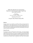
S1
48M
Counter8_PWMPresc
PWM8_Sine0
:32
:16
Counter8_SineGen
Rdac0
24V1 (6MHz)
ClockMux
:N
BPF4_SineGen
PGA_SineGen
PWM8_Sine1
External LPF
Buf1
Anti-aliasing filter
Stimulus Driver
Rdac1
3 different gains
:16
Fs
S2
C1
PWM8_Sine2
Rdac2
Ext DC B
Rout
100
:16
Amp1
Rdiv1
1800
G=1
Rdiv2
200
Measure_Counter8_ADCPresc
Amp2
48M
:M
G=1
Amp3
Measure_ADCINC12
PGA_DemodPreamp
Rref
OP1
Fs
Digital Output
Rlpf
G=1
Clpf
Amp4
Hi/Lo Gain ASA10
sC Demodulator
Zx
ADCInMux
G=1
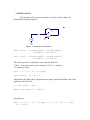
Fig 1.2 Measurement Block Diagram (Everything inside the dashed lines is
located in PSOC)
From Fig. 1.2, the upper part of the diagram is the stimuls generator.
Counter8_SineGen, Counter8_PWMPresc, the three PWM generators and the three
resistors Rdac0..Rdac2 generate a piecewise approximated sine wave (four different
amplitude levels). The bandpass filter BPF4_SineGen, together with the external antialising filter transform the approximated sinewave into a low-distortion sinewave. The
frequency of the sinewave is determined by setting the dividing ration of
Counter8_SineGen, the amplitude is set by the gain of PGA_SineGen. The buffer
amplifier Buf1 drives the component under test, Zx.
The operational amplifier OP1 forms together with a selectable reference
resistor Rref (selected by a set of relays) a current-to-voltage converter. The voltage
across the reference resistor is fed into the PSoC through the two impedance converters
Amp3 and Amp4. Additionally, the voltage across the component under test is
measured seperatly and also fed into the PSoC (four-wire measurement). In order to
increase the measurement range, the drive voltage is divided by Rdiv1 and Rdiv2 and
the gain of the amplifier driving the demodulator ASA10 is adjusted if necessary. The
demodulator's local oscillator input is driven by the square wave output of a PWM
generator, which has the same frequency as the stimulus sine wave. The phase
difference between the stimulus signal and the local oscillator input signal is set by
selecting the phases of two PWM generators among two differnt sets. Two phase shifts
are used, 0 and 90 degrees, as it is necessary to determine the real and imaginary parts
of the component's impedance.
The demodulator is filtered by an RC lowpass in order to avoid a signal with
fast-rising edges at the input of the ADC. The ADC is clocked with a frequency
generated by the Measure_Counter8_ADCPresc which is adjusted in such a way that
the ratio between the integration time of the ADC and the period of the stimulus sine
wave is always an integer.
In the implementation, no multipliers are used, but an amplifier which has a gain
of either +G or -G, and the gain polarity is selected by a square wave LO signal. This
has the disadvantage that the LO signal also contains the harmonics of the carrier
frequency (Fourier series of a square wave), implying that not only the fundamental
frequency component of the demodulator input will be measured, but also its
harmonics. Also, the bandpass filter is not present in this form in the implementation,
but the filtering is mainly performed by the integrating action of an ADC which directly
integrates the multiplier output.
In the measurement circuit, two synchronous quadrature demodulators are used
to measure the amplitudes of Urref and Uzx. Also, Urref and Uzx are measured
differntially, this allows the four-wire connection to Zx and Rref, and also compensates
for the fact that the negative input of the operational amplifier OP1 is in reality not
equal to 0V.
Parasitic impedances between the measurement terminals and ground do not
influence the measurement result to some extend, as the stimulus connection side of the
component under test is driven by a source with a low output impedance, and the input
side of the current-to-voltage converter is kept to 0V by OP1, therefore the current
through any impedance between this point and AC ground is also 0. This makes the use
of shielded probe cables possible.
The internal DC bias is added in front of the filter. Buffer amplifier Buf1 drives
the component under test, Zx. The external DC bias is added after the buffer if S2 is off.
The demodulator is implemented as follows: PSoC block ASA10 is configured
as amplifer with a gain of 31/32, using the A input, with enabled autozero functionality
and AGND as reference. The LO input of the demodulator is enabled by routing the
DCA03 (PWM8_Sine1 output) to the A input polarity switch by setting the appropriate
bits in AMD_CR.
The demodulator output is filtered by an RC lowpass in order to avoid a signal
with fast-rising edges at the input of the ADC. The ADC clock is generated by the
Measure_Counter8_ADCPresc which is adjusted in such a way that the ratio between
the integration time of the ADC and the period of the stimulus sine wave is always an
integer. The same clock also drives the sC clock input of the demodulator. In order to
achieve results which are as reproducible as possible, the phases of the stimulus sine
wave, of the BPF4 filter sampling clock and of the ADC and ASA10 sampling clocks
are all synchronized.
To avoid loosing the phase relationship when restarting the two counters by
software, their enable inputs are externally connected together to a Std CPU output port
which starts both counters at the same time.
As the whole measurement is based on ratiometric measurements, the absolute
accuracy only depends on the reference resistors. All other gain errors are compensated
because the same gain is always used for all measurement channels. DC offset errors
are also eliminated either because the measurement path is AC-based in front of the
demodulator, and offsets after the demodulator are eliminated because Urref and Uzx
are measured as voltage differences, calculated using the ADC results.
In addition to the measurement functions, a RS232 UART is needed for
transmitting the results to a PC. As there are not enough digital PSoC blocks to
implement both functions at the same time, three different PSoC configurations exist. A
basic configuration with the blocks which are common the the measurement and RS232
functions, a 'Measure' configuration which is specific to the measurement functions and
a 'Comm' configuration which is specific to the RS232 functions. If the RS232
functions are needed the 'Measure' configuration is unloaded and the ‘Comm’
configuration is loaded, and vice-versa.
3. FORMULATION
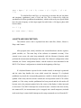
The impedance of Zx can be measured by driving Zx with a voltage and
measuring the current through Zx.
Rref
OP1
Zx
Figure1.3 Impedance measurement
Rser = Rref * (UrrefRe*UzxRe + UrrefIm*UzxRe) /
(UrrefRe^2 + UrrefIm^2)
Xser = Rref * (UzxIm*UrrefRe - UzxRe*UrrefIm) /
(UrrefRe^2 + UrrefIm^2)
The series capacitance or inductance can be derived from Xser.
If Xser < 0, then the reactive part is capacitive, if Xser > 0, inductive.
(f = frequency in Hz):
Cser = -1 / (2 * Pi * f * Xser)
Lser = Xser / (2 * Pi * f)
Additionally, the quality factor, dissipation factor, phase angle and absolute value of the
impedance can be derived:
Q = abs (Xser) / Rser
Zabs = sqrt (Rser^2 + Xser^2)
Cpar and Lpar:
Cpar = -1 / (2 * Pi * f * Xpar) = -1 / (2 * Pi * f * Xser
* (1 + 1/Q^2))
Lpar = Xpar / (2 * Pi * f) = Xser * (1 + 1/Q^2) / (2 * Pi
* f)
To calculate Rser and Xser, it is necessary to measure the real (in phase)
and imaginary (quadrature) parts of Urref and Uzx. This is achieved by using two
synchronous rectifiers (quadrature demodulator), which are driven by two signals which
have the same frequency as their input signal, but which have a 90 degrees phase shift
between them.
D = 1 / Q
ϕ = atan (Xser / Rser)
4.SOFTWARE DESCRIPTION
The software source code is separated into three main files, Main.c, Mesure.c,
Disp.c and Comm.c.
After program start, main() initializes the external hardware and the registers,
global variables, etc. The main loop of the software in contained in main(). If no
external event occurs, the main loop continually calls the Measure() function which
performs the measurement and displayes the results. The 'Measure' configuration is then
unloaded, the 'Comm' configuration loaded, and the results are also transmitted to the
RS232. The 'Mesure' configuration is reloaded at the beginning of the loop.
If a keyboard button is pressed or the encoder rotated, an interrupt is generated
and the main loop handles the event which caused the interrupt. If a keyboard
pushbutton is pressed, the corresponding parameter variable is altered and the display is
updated. If the rotary encoder switch is rotated, the cursor position on the LCD is either
updated, or if the rotary encoder pushbutton has been pressed and the edit mode will
become active, the parameter pointed at by the cursor on the display is either increased
or decreased. If an RS232 interrupt has occurred because a character has been sent by
the connected PC, the measurement cycle is stopped, and a small interpreter (included
in the main loop) is started which interpretes the setup commands received from the PC.
The Measure() function is the most important one, as it handles the whole
measurement and results calculation (2). First the relative demodulator LO phase is set
to 0 degrees, the four PSoC measurement inputs VIN0, 1, 2, 3 (or 4) are converted to a
digital value by the ADC, then the phase is set to 90 degrees and the measurement is
repeated. From these 8 values, 4 differences are calculated and are used to derive all the
measurement results (Rser, Cser, etc) according to the procedure described above. A
user-selectable averaging (1 to 8 measurements) is performed by the function reading
the ADC result in Measure.c.
An autorange function is performed, which uses the measured values as decision
inputs. Depending on the range, either the reference resistors of the current-to-voltage
converter are switched, or the PGA gain in front of the demodulator is increased, or the
attenuated input VIN4 is used instead of VIN3. The functions in Measure.c support the
measurement procedure by setting hardware parameters. Meas_SetSineGenFreq() sets
the carrier frequency as described above. The divider ratios for the Counter8_SineGen
and for the Measure_ADC_Prescaler counters are read from an array 'FreqDivArr'
which is contained in the file Freqarr.c. This file has been generated by the TurbiC
program 'DivCalc.exe' which determines both divider ratios in such a way that the
integral relationship between both divider ratios are kept as described above, and that
the ADC conversion time is as close as the one for which the specified ADC parameters
in the datasheet are valid.
The display functions are contained in Disp.c. The important ones are
Disp_FreqFloatToTmpStr() and Disp_MeasFloatToStr(). The first one converts the
frequency in Hz contained in a float to a formatted string which can be displayed. The
second one converts a measurement result also to a formatted string with four
significant digits and adds multiplier ('p' to 'M').
4. CONCLUTION:
The LCR meter using programmable system on chip (PSOC) is
constructed as hardware device. The software programmes are designed based on the
theoretical analysis and analog and digital block
implementations. The component
(capacitance, inductance, resistance) values are checked using LCR-meter. The LCD
displays the real part (resistance), the imaginary part (capacitance or inductance) and
one selectable third result at the same time.
The usage is simple: switch power on and connect a component under test. The
instrument will autorange to the correct range. If necessary, use the rotary encoder or
keyboard to change:
-
the stimulus frequency,
-
the stimulus AC amplitude
-
the DC bias
-
the averaging length of the measurement display
-
the equivalent circuit mode: parallel or serial
-
the zero trim function to on or off
-
the third result display (Q, D, Phi, or Z^2)
The display looks as follows for example:
| R:100.0kR C:100.0nF
Q:>100
PAR ZERO|
|>F:154.24Hz U:500mVAC ExtVDC Avg:8 REMT|
R
:
resistance,
C (or L)
:
reactive part,
Q (or D, Phi, Z) :
PAR (or SER)
third result, also selectable by pushbutton '3rd'
: equivalent circuit mode, also selectable by pushbutton
'Ser/Par'
ZERO (or ABS) :
zero trim mode on or off, also selectable by pushbutton 'Zero'
F
: Carrier frequency
U:500mVAC
:
Stimulus AC voltage (or 250mV, 1V)
ExtVDC
:
DC bias (or 2.5V, 0V)
Avg:8
:
Averaging length
REMT
:
Instrument is currently in remote mode (parameter setup
by
connected PC). Push rotary encoder to force exit to local mode.
A cursor is displayed (shown as arrow next to the frequency display) which can
be displaced by the rotary encoder. If the encoder is pressed, the edit mode gets active,
and the parameter to which the cursor points at can be changed by rotating the encoder.
Each measurement result is also sent to the RS232.
5. REFERENCES:
1.
Atman and M.A., Jagadeeshkumar V. and Vempati G.K. Muthi (1996), ‘A
microcontroller based quasi-balanced bridge for the measurement of L,C and
R’ IEEE transaction on Instrumentation and Measurement, Vol.45, No.3.
2.
Honda M. (1989), ‘The impedance measurement Handbook. A guide to
Measurement Technology and Techniques’, Yokogawa-Hewlett Packard Ltd.
3.
‘LCR measuring primer’ has dealt in www.quadtech.com.
4.
‘LCR meter user manual’ has been adapted in Stanford Research Systems.