1
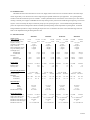
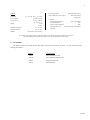
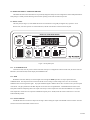
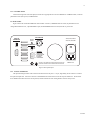
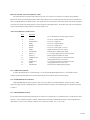
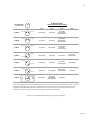
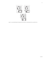
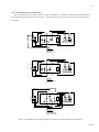
Model 500 Series Laser Diode Driver
User's Manual
1
1.0 INTRODUCTION
The Model 500 Series Laser Diode Drivers are low noise, highly stable current sources for use with laser diodes. Selectable output
current ranges allow you to choose the laser current range having the optimum resolution for your application. Two operating modes,
constant current and constant laser power are available. A monitor photodiode can be zero biased or reverse biased up to 5 volts without
resorting to external power supplies. Redundant FET and relay shorting circuits protect the laser diode during the beginning of a soft-start
sequence. After a short delay the output current slowly ramps up to the operating set-point. A current LIMIT setting unconditionally
protects the output from exceeding the laser diode’s maximum specified operating current independent of operating mode. An external
analog modulation input allows voltage controlling the output and a low cost alternative for remote control and monitoring of the laser
diode can be implemented using the Analog Interface Card.
1.1 SPECIFICATIONS
Model 501
Output Current
Output Current Range (mA)
Set-point Resolution (mA)
Set-point Accuracy
Compliance Voltage (Volts)
Temp. Coefficient
Short Term Stability (30 min.)
Long Term Stability (24 hr.)
Noise/Ripple (rms)
Hi Bandwidth
Lo Bandwidth
Transients
Operational
Power-line spike
Model 505
0 to 500
0.050
± 0.1 % FS
7 Volts
< 50 ppm/°C
< 10 ppm
< 25 ppm
Model 525
Model 560
0 to 1000
0 to 2500
0.100
0.250
± 0.1 % FS
7 Volts
< 50 ppm/°C
< 10 ppm
< 25 ppm
0 to 3000
0 to 6000
0.300
0.600
± 0.1 % FS
5 Volts
< 100 ppm/°C
< 20 ppm
< 50 ppm
0 to 50
0 to 100
0.005
0.010
± 0.1 % FS
7 Volts
< 50 ppm/°C
< 10 ppm
< 25 ppm
0 to 200
0.020
< 2 µA
< 1 µA
< 2 µA
< 1 µA
< 4 µA
< 2 µA
< 4 µA
< 2 µA
< 8 µA
< 4 µA
< 20 µA
< 10 µA
< 50 µA
< 25 µA
< 200 µA
< 50 µA
< 1 mA
< 5 mA
< 1 mA
< 5 mA
< 1 mA
< 5 mA
< 1 mA
< 5 mA
< 2 mA
< 10 mA
< 5 mA
< 10 mA
<10 mA
< 20 mA
< 25 mA
< 50 mA
0 to 999.9
0.1
±1
0 to 2500
1.0
±3
0 to 3000
1.0
±5
0 to 6000
1.0
± 10
Current Limit
Range (mA)
Resolution (mA)
Accuracy (mA)
0 to 50.00
0.01
± 0.1
0 to 99.99
0.01
± 0.1
0 to 200.0
0.1
± 0.5
0 to 500.0
0.1
± 0.5
External Analog Modulation
Input
Transfer Function
Bandwidth
Hi BW (kHz)
Lo BW (kHz)
0 to 10V, 10 kΩ
5 mA/V
10 mA/V
0 to 10V, 10 kΩ
20 mA/V
50 mA/V
0 to 10V, 10 kΩ
100 mA/V
250 mA/V
0 to 10V, 10 kΩ
300 mA/V
600 mA/V
DC - 1000
DC - 10
DC - 500
DC - 10
DC - 300
DC - 10
DC - 150
DC - 10
DC - 750
DC - 10
DC - 350
DC - 10
DC - 200
DC - 10
DC - 100
DC - 10
Photodiode Input
Monitor Current
Range
Stability
Accuracy
Photodiode Bias Voltage
Measurement Display
Output Current Range (mA)
Output Current Resol. (mA)
Output Current Accuracy
Photodiode Current Range (µA)
Photodiode Current Resol.(µA)
Photodiode Current Acc.
0 to 5 mA
± 0.02 %
± 0.1 %
0 to 5 Volts
0 to 5 mA
± 0.02%
± 0.1 %
0 to 5 Volts
0 to 50 mA
± 0.02 %
± 0.1 %
0 to 5 Volts
0 to 50 mA
± 0.02 %
± 0.1 %
0 to 5 Volts
0 to 50.00
0 to 99.99
0.01
0.01
± 0.1 % of full scale
0 to 5,000
1.0
± 0.1 % of full scale
0 to 200.0
0 to 500.0
0.1
0.1
± 0.1 % of full scale
0 to 5,000
1.0
± 0.1 % of full scale
0 to 999.9
0 to 2500
0.1
1.0
± 0.1 % of full scale
0 to 50,000
1.0
± 0.1 % of full scale
0 to 3000
0 to 6000
1.0
1.0
± 0.1 % of full scale
0 to 50,000
10
± 0.1 % of full scale
4/10/00
2
Laser Safety Features
(Meets CDRH US21 CFR 1040.10)
General
Input Power
Chassis Ground
Size, H x W x D
Weight
Operating Temperature
Storage Temperature
Humidity
90 - 125, 180 - 250 Vac, 50 - 60 Hz
4 mm banana jack
88 x 215 x 280 mm
(3.5” x 8.5” x 11”)
2.9 kg
(6.5 lbs.)
0°C to +50°C
-40°C to +70°C
< 90% relative, non-condensing
Output On/Off Keyswitch
Rear Panel Interlock
Output Delay
Connectors
Laser Diode & Photodiode
9-pin, D-sub (female)
External Photodiode
BNC
External Analog Modulation
BNC
Analog Interface Card
15-pin, high density D-sub (female)
(Optional)
In accordance with ongoing efforts to continuously improve our products, Light Control Instruments, Inc. reserves
the right to modify product specifications without notice and without liability for such changes.
1.2 ACCESSORIES
The Model 500 Series Laser Diode Drivers come with a line cord for connection to AC power. To order accessories use the
following part numbers:
PART #
DESCRIPTION
500-02
Laser Diode Driver Cable
500-04
Laser Diode Driver/Mount Cable
500-60
Analog Interface Card
500-70
Rack Mount Kit
4/10/00
3
2.0 MODEL 500 SERIES LASER DIODE DRIVERS
The Model 500 Series Laser Diode Drivers are specifically designed to safely drive all configurations of laser diode/photodiode or
LED packages. Carefully read the following sections before operating a laser diode or LED with your unit.
2.1 FRONT PANEL
The front panel (see Figure 1) of the Model 500 Series Laser Diode Driver is logically arranged for easy operation. Seven
distinct areas, each with a specific set of related functions, and the control knob are located on the front panel.
MODEL 501 LASER DIODE DRIVER
LASER
ENABLE
OFF
DISPLAY
ON
PRESET
CURRENT
POWER
mA
LIMIT
POWER
MOD
EXTERNAL
INPUT
RANGE
50 mA
100 mA
MODE
I
OUTPUT
P
ON
ERROR
LIMITING
LIMIT SET
5 mA/V
10 mA/V
Figure 1: Front panel layout.
2.1.1 AC POWER SWITCH
Located lower left, when AC power is turned on the unit comes up in a configuration with the OUTPUT off, the lower of the two
RANGE’s, the I mode selected, and the display in the PRESET mode.
2.1.2 MOD
Modulation of the laser diode by an external signal source through the MOD input BNC can only be performed in the
CURRENT mode. The output current level to the laser diode can be set using a constant voltage source or it can be externally
modulated with a function generator signal. Any input modulation signal is added to the DC drive current level set by the front panel
control knob. The gain printed below the BNC depends on selection of low or high RANGE. A bandwidth selection switch on the
back panel introduces a dampening filter in the output control loop to reduce output noise when external modulation is not required.
If the output drive current does not respond to a modulation frequency above 10 kHz, check the switch to make sure it is not in the
LOW bandwidth position.
2.1.3 RANGE SWITCH
Each Model 500 series unit has two output current ranges. Before turning the output on the RANGE must be selected. Once the
OUTPUT is turned on the RANGE switch is inactive.
4/10/00
4
2.1.4 MODE SWITCH
The Model 500 Series Laser Diode Drivers have two modes of operation; constant current (I) and constant optical power (P).
Mode selection can only be made if the OUTPUT is off. The mode switch is deactivated under output on condition.
In the “I” mode the output drive current to the laser diode is held at a constant level. The output of the laser diode can be
modulated in this mode by connecting an external signal source to the MOD input on the front panel.
The Model 500 series can be used with a monitor photodiode and operated in a constant optical power mode. Reverse voltage
biasing of the photodiode is a standard feature which improves the dynamic range and frequency response of a laser diode. In the “P”
mode the output current to the laser diode is controlled in response to the monitor photodiode current to maintain a constant output
optical power. As a laser diode ages or the temperature of the laser diode increases more output drive current is required to maintain a
constant optical power level. The LIMIT prevents the laser diode from exceeding its maximum current rating. The laser diode cannot
be modulated in the POWER mode.
2.1.5 OUTPUT SECTION
2.1.5.1 OUTPUT On Switch and Indicator
This switch will activate the ON LED and allow current flow to the laser diode after a three second delay, assuming it is correctly
connected, the “LASER ENABLE” keyswitch is activated, and pin 1 and 2 of the back panel interlock feature are shorted.
2.1.5.2 ERROR Indicator LED
Certain conditions will cause the red ERROR LED and it’s protection circuitry to activate, automatically shutting off the output:
A. An open circuit in the laser diode package or cabling.
B. Forward voltage drop of laser diode (or series arrangements of multiple diodes) exceeds the compliance voltage
specified in Table 1.1.
C. Overmodulating the external voltage input to cause laser output current to exceed the previously set limit value.
Once the fault is corrected, the OUTPUT ON switch must be pushed once to clear the error indication, and a second time to
restore current to the laser diode.
4/10/00
5
2.1.5.3 LIMITING Indicator LED
A soft limit occurs when output current gradually exceeds a preset value, clamping flow at that level and causing the LIMIT LED
to blink until the threshold is no longer exceeded A hard limit, indicated by solid green LED and an ERROR light can occur if
overmodulating the external input when first attempting the turn on the output. The error must be cleared before normal operation can
occur.
2.1.5.4 LIMIT SET
A small slotted screwdriver is used to access a recessed trimpot to adjust the unit’s output current limiting level. Toggle the
DISPLAY section push-button to the LIMIT indicator and adjust the readout with a clockwise rotation to increase the appropriate
protection level.
2.1.5 LASER ENABLE
This key switch is a safety feature that prevents the OUTPUT from being turned on by unauthorized curious fingers. The key may
only be removed in the OFF position.
2.1.6 DISPLAY SECTION
The LED display located in the top center of the front panel is a four digit green array. It reads current in mA for all four models.
Pushing the momentary switch cycles through display values as described below. Display modes can be toggled with the output on or
off.
2.1.3.1 PRESET Display
This mode allows setting diode milli-Amp levels with the control knob before actually turning on the output.
2.1.3.2 CURRENT Display
This readout measures actual current flow in milli-Amps to the laser diode, it’s level will drop to zero with output off. The display
shows average output drive current if modulated from a varying external input waveform.
2.1.3.3 POWER Display
Using the monitor photodiode current (Im) displayed, a conversion table supplied by the diode manufacturer will indicate actual
optical power level.
2.1.3.4 LIMIT Display
This value is set by the LIMIT set screw adjustment. See Section 2.1.5.4. The output drive current will not exceed this LIMIT
value regardless of operating mode.
4/10/00
6
2.1.5 CONTROL KNOB
Located on the right side of the front panel, this knob set an appropriate drive current in PRESET or CURRENT mode, or monitor
photodiode current (laser power) in POWER mode.
2.2 REAR PANEL
Figure 2 shows the ANALOG INTERFACE and OUTPUT connectors, a REMOTE/LOCAL switch, the photodiode reverse
voltage BIAS ADJUST screw, a photodiode BNC input, the BANDWIDTH selection switch, and the AC power inlet.
ANALOG
INTERFACE
REMOTE
PHOTODIODE
115/230, 2A/1A, 60/50 Hz
250V, 3AG, SLO-BLOW
PD BIAS
ADJUST
BANDWIDTH
LOCAL
115 V
HIGH
LOW
OUTPUT
1,2
3
4,5
6
7
8,9
INTERLOCK
CHASSIS GND
LASER CATHODE
PD CATHODE
PD ANODE
LASER ANODE
CAUTION: DO NOT REMOVE COVER, REFER SERVICING TO QUALIFIED
PERSONNEL. DISCONNECT INPUT POWER BEFORE REPLACING FUSE
MADE IN U.S.A.
Figure 2: Rear panel layout.
2.2.1 ANALOG INTERFACE
The optional Analog Interface Card is located at the far left of the rear panel. A 15-pin, high density, D-sub connector is used for
the input and output lines. Above the connector is the REMOTE ON switch used to activate the set-point enable line. The Set-Point
line is disabled when this switch is in the off position, all other status lines of the Analog Interface Card are always active.
4/10/00
7
HOW TO USE THE ANALOG INTERFACE CARD
The Analog Interface Card may be used with chart recorders, X-Y recorders or be operated via a computer using a multiple
function I/O card such as National Instruments LAB-PC data acquisition card. One data acquisition card will control two Model 500
units or one Model 500 and one Model 300 unit. The Output Set-point is set using one of the analog outputs from the data acquisition
card. Other TTL signals of the Analog Interface card are interfaced to the digital I/O lines. R/T Monitor data, such as the temperature,
is then acquired using the analog input line of the data acquisition card.
ANALOG INTERFACE CONNECTIONS
Pin #
1
Description
ON/OFF
TTL or Momentary Low pulse toggles OUTPUT
2
ENABLE
TTL (Low = Remote Enabled)
3
4
5
6
7
8
ON/OFF Status
LIMIT
ERROR
MODE
DGND
EARTH GND
TTL (Low = Output On)
TTL (Low = Output Limiting)
TTL (Low = Output Error)
TTL (Low = Power, High = Current)
Digital ground return for TTL signals
Earth ground for shielding TTL signals
9
10
LEVEL (+)
LEVEL (-)
0 - 10 V input signal bypasses front panel control
Return signal for external level control
11
CURRENT OUT
0 - 10 V signal represents 0 to full range selected
12
13
14
15
AGND
POWER OUT
AGND
EARTH GND
Analog ground return for Current Out
0 - 10 V signal represents 0 to full range selected
Analog ground return for Power Out
Earth ground for shielding Analog signals
2.2.2 PD BIAS ADJUSTMENT
A monitor photodiode may be reversed biased up to 5 volts using the PD BIAS adjustment screw. In the farthest counterclockwise position the photodiode is zero biased while turning the screw clockwise increases the bias voltage.
2.2.3 BANDWIDTH SELECT SWITCH
LOW bandwidth dampens output response to reduce noise levels between 0-10 kHz modulation. Frequencies above 10 kHz
require fast output response in the HIGH position. Maximum modulation frequency varies depending on drive capabilities specified
in Table 1.1.
2.2.4 PHOTODIODE BNC INPUT
For use with a stand-alone photodiode arrangement, this connector is in parallel with pin 6 (cathode) and pin 7 (anode) of the D-Sub 9
connector. Center terminal of the BNC is cathode. Outside shell is anode and is isolated from the chassis. PD bias adjustments are
made with the (+) side of a DC voltmeter to cathode, and (-) side probe to anode. (0 to +5 VDC scale)
4/10/00
8
2.2.5 OUTPUT CONNECTOR
Pin connections to the laser diode and monitor photodiode are made from the 9-pin, D-sub connector labeled OUTPUT. The
connections are printed on the rear panel and should be made as shown in figures 4 or 5.
Pin #
Description
Wire Color (Part # 500-02)
Interlock
Shorting jumper or external closure
Chassis Gnd
Shield or drain wire
Laser Cathode
Black
6
Photodiode Cathode
White
7
Photodiode Anode
Green
Laser Anode
Red
1,2
3
4,5
8,9
2.2.5 CHASSIS GND
This 4 mm banana jack, connected to chassis ground, is intended to be used as a common reference ground for the laser diode
case. (Pin 3 of the output connector may also be used)
2.2.6 AC POWER INLET
The input voltage setting is indicated in a small window on the face of the power module. A small screwdriver is needed to flip
down a panel once the AC line cord is removed. Carefully pry out the plastic tumbler and reinsert it to show the approximate power
grid voltage. The fuse is also located behind this panel and can be pulled out and replaced with the appropriate size indicated on the
back panel.
All units are preset at the factory for operation from 90-125 VAC, 50/60 HZ, unless otherwise notified by the purchaser. A line
cord supplied with each unit should be plugged only into a three prong properly grounded outlet to prevent electrical shock in the
event of internal short circuit to the metal cabinet.
4/10/00
9
3.0 MODEL 500 SERIES OPERATION
Operating procedures of the Model 500 Series Laser Diode Drivers include safe handling procedures for laser diodes, various
types of laser diode packages, how to make the connections, and how to earth ground a laser diode.
3.1 LASER DIODE HANDLING PRECAUTIONS
Laser diodes are extremely sensitive to static discharge and guidelines should be followed at all times when handling laser
diodes:
a) all operators must have a properly grounded wriststrap before handling any laser diode.
b) all soldering iron tips must be properly grounded.
c) all related test and assembly equipment must be properly grounded
Laser diodes are extremely sensitive to electrostatic discharge since they can only withstand a maximum reverse voltage of 2 to 3
V across their leads and no more than the maximum rated current in the forward direction. Always follow the manufacturers
instructions for removing and handling laser diodes.
Additional precaution must be taken when soldering leads of a laser diode.
Excess heat from soldering damages the laser facet. Care must be taken to provide a heat sink between the laser diode and the leads
during soldering. Always follow the laser diode manufacturer's specifications for maximum temperatures and soldering times.
3.2 LASER DIODE CONNECTIONS
Laser diodes come in many different types of packages, with and without monitor photodiodes. The following sections will show
how to make connections to standard 9mm and 5.6mm packaged laser diodes and also telecommunication laser diodes in DIL and
butterfly packages. Any other packages such as TO-3 packages have laser diode and photodiode connections identical to the types
shown.
3.2.1 9mm and 5.6mm Laser Diode Packages
Almost all CD style packages fall into one of seven configurations as shown in figure 3. Figure 4 shows how to connect a
Model 500 unit to three configurations of laser diode and photodiode. The optional chassis ground (earth ground) should not be
connected until reading section 3.3.
4/10/00
10
Pin assignment
from pin side
1
3
9 mm & 5.6 mm
Laser Diode Pin Connections
2
4
Laser Diode
Pin 1
Pin 2
Pin 3
LD Cathode
PD Anode
LD Anode,
PD Cathode,
Case Common
LD Anode
PD Anode
LD Cathode,
PD Cathode,
Case Common
LD Anode
PD Cathode
LD Cathode,
PD Anode,
Case Common
LD Cathode
PD Anode
PD Cathode
LD Anode,
Case Common
LD Cathode
PD Anode
LD Anode,
Case Common
PD Cathode
PD Anode
LD Cathode
PD Cathode,
Case Common
LD Anode
LD Cathode
LD Anode
PD Cathode
Case Common
PD Anode
Photodiode
TYPE A
Laser Diode
Photodiode
TYPE B
Laser Diode
Photodiode
TYPE C
Photodiode
TYPE D
Laser Diode
Laser Diode
TYPE E
Photodiode
Photodiode
TYPE F
Pin 4
Laser Diode
Photodiode
TYPE G
Laser Diode
Notes: Pin assignments for some laser diodes may differ from those shown. Please be careful and check for the correct laser
diode type before making any connections to a Model 500 Series Laser Diode Driver. If the laser diode is to be earth
grounded the CHASSIS GND from the laser diode driver is used to make this connection and is connected the Case
Common pin. Make sure that this is the only earth ground connection to the laser diode.
Figure 3: Laser Diode/Photodiode package types with pin assignments.
4/10/00
11
Type 1 (4,5,6): LD Anode, PD Cathode, case common
LD
Type 2: LD Cathode, PD Cathode, case common
PD
LD
PD
Optional Chassis
(earth) Ground
5
1
9
6
Optional Chassis
(earth) Ground
Model 500 Series
Output Connector
5
1
9
6
Model 500 Series
Output Connector
Type 3: LD Cathode, PD Anode, case common
LD
PD
Optional Chassis
(earth) Ground
5
1
9
6
Model 500 Series
Output Connector
Figure 4 Laser Diode/Photodiode configurations and connections to Model 500 Series Laser Diode Drivers.
4/10/00
12
3.2.2 Telecommunication Laser Diode Packages
Most telecommunication laser packages fall into one of three configurations. Connections of a Model 500 and Model 300 unit to
a telecommunication laser package are shown in Figure 5. Care must be taken when connecting the chassis ground (earth ground) to
the package.
8
5
1
PD
9
14
LD
6
TE
TH
Case
GND
8
15
1
9
1
7
TYPE "A"
Lasertron (DIL)
Mitsubishi (DIL)
BT&D (DIL)
8
5
1
PD
9
14
6
LD
TE
TH
Case
GND
8
15
1
9
1
7
TYPE "B"
Alcatel (DIL)
Toshiba (Butterfly)
OKI (DIL)
8
5
9
14
LD
1
Case
GND
TE
PD
6
8
1
TH
15
9
1
7
TYPE "C"
AT&T (Butterfly)
Lasertron (Butterfly)
Mitsubishi (Butterfly)
Figure 5: Telecommunication laser diode packages and connections to Model 500 Series Laser Diode Drivers.
4/10/00
13
3.3 GROUNDING A LASER DIODE
The outputs of the Model 500 series are isolated from earth (chassis) ground. In an ideal environment, keeping the laser diode
case isolated avoids damaging the device from multiple ground loop potentials, AC transients or static discharge. Since test
equipment probes, signal sources and package mounts are often partially earth grounded in the real world, it is often necessary to also
bond the device case to earth ground. It is strongly recommended that a single point ground scheme be established, specifically at
either pin 3 of the DB-9 connector or the binding post on back of the rear panel. This will help minimize noise, transients, and ground
loop hazards.
Basically, you, as the user and supplier of the laser diode, are most familiar with your own setup, and must make an informed
decision as to the best hookup arrangement to avoid damaging the device. If you have additional questions about an esoteric earth
grounding method contact an applications engineer here at Light Control Instruments, Inc.
3.4 MODEL 500 SERIES SETUP
3.4.1 USING THE INTERLOCK FEATURE
The interlock feature is essentially an additional dry contact closure in series with the front panel keyswitch. The loop between
pins 1 and 2 can be remoted as a relay contact or safety switch which disables the output drive circuit when opened. Once the interlock
loop is again closed, pushing the front panel OUTPUT switch will resume current flow after a three second soft-start sequence. The
switch or relay contact should be electrically isolated from all other circuits and earth ground.
3.4.2 RACK MOUNTING MODEL 500 SERIES UNITS
Two units, either Model 300’s or Model 500’s or one of each, may be mounted in the standard rack mount kit (part #500-70).
Once the feet are removed, use the screws supplied with the rack mount kit and secure the bottom wrap to the bracket using the two
original front feet mounting positions. After tightening the screws the unit (s) may be slid into a 19” rack and secured to the side rails.
4/10/00
14
3.4.3 MODEL 500 SERIES OPERATING CHECKLIST
The following step by step procedure should be followed when operating a Model 500 Series Laser Diode Driver:
a) Check the AC voltage selection of the controller to be sure that it is compatible with the outlet to be used. All
units are factory preset for operation from 90-125 VAC.
b)Verify that the interlock feature has been enabled, pins 1 & 2 of the OUTPUT connector must be shorted
before the unit will allow the output current to flow to the laser diode.
c) If using the optional Analog Interface Card connect it to a computer and change the ANALOG INTERFACE
switch to the REMOTE position.
d) Turn the unit on and allow it to warm up.
e) Select RANGE of operation.
f) Set the LIMIT set point via the recessed limit set screw on the front panel.
g) Connect the laser diode and photodiode as described in sections 3.1 - 3.3.
h) Adjust the PD BIAS voltage to the photodiode.
i) Select either CURRENT or POWER mode
j) Select PRESET display mode and set output current or monitor photodiode (optical power) level using the front
panel control knob.
k) Enable KEYSWITCH, push OUTPUT on Switch, then toggle front panel display to appropriate readout.
NOTICE
LIGHT CONTROL INSTRUMENTS IS NOT IN ANY WAY RESPONSIBLE FOR ANY DAMAGE TO ANY DEVICE USED
IN CONJUNCTION WITH THE MODEL 500 SERIES PRODUCTS.
4/10/00
15
4.0 CALIBRATION PROCEDURE
Your equipment may be returned to the factory for calibration and maintenance, or may be accomplished in your own testing lab.
Recommended equipment or equivalent:
Description
Manufacturer / Model
Specification
Digital Multimeter
Fluke 45
DC current (10 µA resolution), +/- 0.1%
DC voltage +/- 0.1% @ 2.000V
RESISTANCE +/- 0.001%
Precision Resistor
Metal Film
40Ω, 1/2 W, 0.05% (Model 501)
10Ω, 1 W, 0.05% (Model 505)
2Ω, 3 W, 0.05% (Model 525)
0.667Ω, 5 W, 0.05% (Model 560)
A. Remove four screws and lift off top cover.
B. Place precision resistor across pins 5 and 9 of output connector.
C. Short pins 1 and 2 of connector with small jumper.
D. On back panel select low bandwidth mode.
E. Turn on AC switch and let unit warm up for 5 minutes.
F. Set up DC voltmeter to measure TP4 MOD with respect to AGND on analog board (vertical board with output
connector). Adjust R8 to read 0.000 ± 0.001.
G. Activate laser enable keyswitch.
H. Place display in CURRENT position, select I MODE, keep RANGE in lower setting, and rotate
main control knob fully counter-clockwise.
I. Set up voltmeter to measure “TP2” with respect to AGND lug on analog board.
J. Turn OUTPUT on and adjust front panel control knob to read 1.000 + .003 VDC on voltmeter.
K. This step applies only to a Model 505 or 560. Move positive voltmeter probe to test point DISP on front panel
board. It should read 1.000 ± 0.003 as in previous reading. Change the display to PRESET and adjust R23 of analog
board to read the same value. Return display to CURRENT after adjustment is complete.
L. Push OUTPUT off and move voltmeter to measure across precision load resistor.
M. Turn OUTPUT on and adjust R37 of analog board for 1.000 + .003 VDC across output resistor.
N. With output still on, adjust R4 on front panel board to read one of the following values on the
LED display.
MODEL 501: 25.00 + .01 mA
MODEL 525: 500.0 + 0.1 mA
MODEL 505: 100.0 + 0.1 mA
MODEL 560: 1500 + 1.0 mA
O. Calibration is now complete.
4/10/00