1
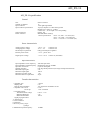
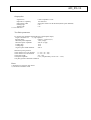
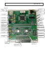
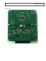
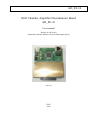
AD_FE-16
Drift Chamber Amplifier Discriminator Board
AD_FE-16
User manual
Release #1 (08/03/06)
Prepared by Nikolay Bondar (e-mail: [email protected])
AD16_H
PNPI
2006
AD_FE-16
Introduction
The Anode Amplifier Discriminator Board AD_FE-16 was designed for amplifying and discriminating anode signals
from Drift Chambers (DC). The board is optimized for the PNPI made Hexagonal Drift Chambers. The essential feature of
the board is integration of analog part and digitizer with sufficient time resolution (RMS less then 2 ns).
Construction
The AD_FE-16 module consists of a printed board assembled with all its components. The board is splited for two
areas – analog and digital. Analog part is closed with a copper shield. Analog area has 16 channel input signal protection
networks, two ASDQ ASIC’s and attendant components. Input connector is a 17X2 socket. The top row of the input
connector is a ground connection; the bottom row has input contacts. Digital part is a 16 channel time digitizer and a serial
line interface. Also the digital part serves analog part with threshold voltage and test facility. Output connector RJ45 is used
for connecting the board with the Concentrator Board. Power connector is a Molex 3X2 pins.
Circuit diagram
The analog part of the AD_FE-16 module consists of the two ASDQ chips (U1, U2), second stage of input protection
network and the ASDQ serving networks.
The input protection network for each channel consists of two stages. The first stage of protection network is located directly
on the chamber (at special connection and protection board) and consists of bulk resistor (51ohm) two limiting diodes and
second SMD resistor (10 Ohm). The second stage of limiting diodes is located at the AD_FE-16 board after input connector.
Amplifier inputs are connected sensor wires with decoupling capacitors.
To provide stable characteristics of the boards, voltage regulators LT1175 (U3) for -3.1V and TK1230 U4) for +3V are used.
Both regulators have a current overflow protection, overheating protection and a power on/off control feature (standby mode).
Minimum 2,0V is a “Power-ON” signal. The input power voltage ranges are +4.0V - +5,0V and -4,5V - -5,0V. The output
voltages of the regulators are: +3,0+/-0,05V and – 3,1+/-0,1V.
The discriminator threshold control voltages come from digital part of the board via voltage followers (U5 AD8534). Its range is 0 - 1.0 V. To minimize threshold variation in one board two threshold control voltages (THR1 and
THR2) are generating for two ASDQ chips.
The board has an internal test feature. Test signal amplitude levels for odd (TREFO) and even (TREFE) channels are
generated at the digital part of the board and go to ASDQ via voltage followers (U5 -AD8534). Test signal width pulses
(TSTN and TSTP) also generated at the digital part at the board.
Each ASDQ chip has its individual service network. There is possibility to use BLR monitor by connecting jumpers J7, J8.
. The AD_FE-16 output signals are LVDS compatible.
Digital part is based on FPGA SPARTAN XC3S200 (XILINX). There are Serial Interface, Time-to-Digital Coder
with time bin 2,5ns, and threshold control and test facility implemented into this chip.
Application note
As far as the AD_FE-16 board is a computer controllable module it cannot work without interface.
AD_FE-16
Troubleshooting
All boards after production are carefully tested.
In case of problems:
- Connect board to the interface.
- Switch on power
- Initialize the board
- Check the power voltages (+4,5V – +6,0V), (4,5V – 6,0V) (+3,3V +/-0,05)
- Check the “Power ON” signal (3,0V).
- Check the board consuming current. It should be +4,5 – 140 mA; -4,5V – 160 mA and +3,3V ~500 mA .
- Check the threshold voltage on the board
- Apply external test pulse to the input pin (negative step V~10 mV via capacitor ~3pF – total injecting charge Qin~ 30 fC)
If all voltages are normal, try to watch the output pulse with an oscilloscope (use high impedance probe).
If there is no output pulse on the board, the board needs maintenance.
AD_FE-16
AD_FE-16 specification
General
Size
Number of channels
Input connector
Input connector specification
Output connector
Power connector
86mm x 106mm
16
17X2 right angle header
Top layer all pins are connected to ground.
Bottom layer: contact 2 – ground,
contacts 4,6, -, 34 are inputs 1-16 corresponding.
RJ45-8_VH
MINIFIT Molex 43045_6
Contact specification:
Pin 4 - -5V; Pin1 - -5V return (0V)
Pin 5 - +5V; Pin2 - +5V return (0V)
Pin 6 - +3.3V; Pin 3 +3.3V return (0V)
Power characteristics
Analog positive voltage
Analog negative voltage
On board power protection
Remote power switch
+4.0 V – 5V
Current 0.15A
-4.5 V – 5V
Current 0.16A
Fully protected power regulator
+3.5 V – power “ON”
Digital power voltage
+3.3 V +/-0.1V
Current 1A (maximum)
Input characteristics
Input impedance at low frequency
Input impedance at high frequency
Input DC connection
Sparkle protection
Minimum input signal
Maximum input signal
Maximum overflow signal
Maximum detector capacitance
300 Ohm equivalent
Rolled off by 30% by 30 MHz
Capacitor decoupled
One stage diode protection (two stages with protection board)
5 fC
100 fC
1 pC
25 pF
Transfer characteristics
* Amplifier gain
Shaping time
Detector tail cancellation
* Amplifier noise Cin=0
Cin=30 pF
* Threshold control
Threshold control voltage
Minimum threshold
Maximum threshold
Signal propagation time
** Slewing time
** Time resolution
** Dead time
** Recovery time @10 pC
@100 pC
** Maximum test pulse frequency
7 mV/fC
6 ns
Two exponents cancellation circuit
0.3 fC
1.2 fC measured
0.08 V – 1.0 V
5 fC
150 fC
10 MHz
AD_FE-16
Output pulse:
Signal levels
Output driver capability
Output pulse width
Leading edge
Trailing edge
** Cross talk level
LVDS compatible 1.5 mA
110 Ohm load
Input pulse width over the threshold (dE/dx option disabled)
6 ns
6 ns
Test Pulse parameters
For external test (should be applied directly to the amplifier input):
Negative transition via
3,.3 pF capacitor
Injected charge
Qin(fC)= 3,3(pF)*U(mv)
Minimum pulse amplitude
1 mV (3.3fQ)
Maximum pulse amplitude
500 mV (1.6pQ)
Leading edge
10 ns
Trailing edge
10 ns
Negative pulse width minimum
500 ns
Internal test pulse generator:
Calib. reference for even channels
0 - -3V (-3V – off)
Calib. reference for odd channels
0 - -3V (-3V – off)
Calib. Pulse width
5ns – 15ns
Calib pulse amplitude
0.6V (complementary levels -0.2V - -0.6V)
Test pulse generator should be calibrated
Notes:
*) Parameters are tested for each board.
**) Parameters should be tested
AD_FE-16
ASDQ chip pin specification
Pin
1
2
3
4
:
15
16
17
18
19
20
21
22
23
24
25
26
27
28
29
30
31
32
33
34
35
35
:
47
48
49
50
51
52
53
54
55
56
57
58
59
60
61
62
63
64
Name
IN1A
IN1B
IN2A
IN2B
:
IN8A
IN8B
AGND
AGND
SUBA
VPP
VCP
ATTN
IBLRM
BLB
BLA
VES
QTHR
ID
VED
VCD
DGND
VEDR
D8B
D8A
D7B
D7A
:
D1B
D1A
VEDR
AN3V
VCD
QEN
QDR
VED
DTHR
VCS
IBLR
TREFE
TREFO
TSTP
TSTN
AN3V
AGND
AGND
Nominal
0.69V =/- 003V
0.69V =/- 003V
0.69V =/- 003V
0.69V =/- 003V
:
0.69V =/- 003V
0.69V =/- 003V
0
0
-3.1V+/- 0.1V
-1.1V
+3.0V+/- 0.1V
0
0
0
- 3.07V
-1.59V
+0.68V+/-0.02V
-3.03V
+2.92V
0
-2.88V
1.24V
0.75V
1.24V
0.75V
:
1.24V
0.75V
-2.88V
-3.2V
+2.92V
+2.94V
-2.23V
-3.0V
+0.17V
+2.94V
-0.76V
-3.0V
-3.0V
-0.5V
-0.29V
-3.20V
0
0
Description
Ch1 Negative going input
Ch 1 Positive going input
Ch2 Negative going input
Ch2 Positive going input
:
Ch8 Negative going input
Ch8 Positive going input
Preamplifier reference
Preamplifier reference
Analog Substrate,
Input protection raile
Preamplifier supply
Attenuate input by 2, ( NO att - V=0
BLR monitor current reference
BLR monitor A
BLR monitor B
Shaper&BLR
Trailing edge tracking control
Output current reference
Discriminator dE/dx
Discriminator dE/dx & Driver
Discriminator &dE/dx ground
Driver supply
Ch8 Driver out negative going
Ch8 Driver out positive going
Ch7 Driver out negative going
Ch7 Driver out positive going
:
Ch1 Driver out negative going
Ch1 Driver out positive going
Driver supply
Analog negative power
Discriminator dE/dx & Driver
dE/dx enable ( +3V= Off)
dE/dx cup drain ref ( -3v = Off)
Discriminator dE/dx
Tracking Discriminator Thershold
BLR current reference
Calib ref for even channels (-3V= 0ff)
Calib ref for odd channels (-3V= 0ff)
Positive going calib pulse edge
Negative going calib pulse edge
Analog Negative Voltage
Preamplifier reference
Preamplifier reference
Comments
Ground connected to detector
Ground connected to detector
Analog minimum voltage
Attenuation is Off (Max. Gain)
Normal - not connected
Disabled
Disabled
Here -3.1V +/- 0.15V
dE/dx disabled
dE/dx disabled
Normal – Off
Normal – Off
Ground connected to detector
Ground connected to detector
AD_FE-16
Top view.
Interface
connector
Power
connector.
JTAG
connector
+3.3V point
DAC
+2.5V point
-TREFO
+1.2V point
Thr 2
Power “ON”
voltage
Thr 1
-TREFE
+4.5V point
BLR monitor ON
+3V point
Attenuation X2
-4.5V point
Threshold 2
-3V point
Threshold 1.
ASDQ 1.
ASDQ 2.
Input connector.
AD_FE-16
Bottom view