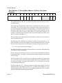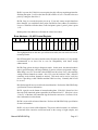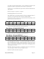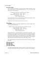
1
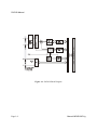
ACCES I/O PRODUCTS INC
10623 Roselle Street, San Diego, CA 92121
TEL (858)550-9559
FAX (858)550-7322
MODEL PAD128
USER MANUAL
FILE: MPAD128.D1g
Page ii
Notice
The information in this document is provided for reference only. ACCES does not assume any liability
arising out of the application or use of the information or products described herein. This document may
contain or reference information and products protected by copyrights or patents and does not convey any
license under the patent rights of ACCES, nor the rights of others.
IBM PC, PC/XT, and PC/AT are registered trademarks of the International Business Machines Corporation.
Printed in USA.
© Copyright 2001 by ACCES I/O Products Inc, 10623 Roselle Street, San Diego, CA 92121. All rights reserved.
U.S. Patent No.s 4,603,320 and 4,972,470.
Page iii
Warranty
Prior to shipment, ACCES equipment is thoroughly inspected and tested to applicable specifications.
However, should equipment failure occur, ACCES assures its customers that prompt service and support
will be available. All equipment originally manufactured by ACCES which is found to be defective will be
repaired or replaced subject to the following considerations.
Terms and Conditions
If a unit is suspected of failure, contact ACCES' Customer Service department. Be prepared to give the unit
model number, serial number, and a description of the failure symptom(s). We may suggest some simple
tests to confirm the failure. We will assign a Return Material Authorization (RMA) number which must
appear on the outer label of the return package. All units/components should be properly packed for handling
and returned with freight prepaid to the ACCES designated Service Center, and will be returned to the
customer's/user's site freight prepaid and invoiced.
Coverage
First Three Years: Returned unit/part will be repaired and/or replaced at ACCES option with no charge for
labor or parts not excluded by warranty. Warranty commences with equipment shipment.
Following Years: Throughout your equipment's lifetime, ACCES stands ready to provide on-site or in-plant
service at reasonable rates similar to those of other manufacturers in the industry.
Equipment Not Manufactured by ACCES
Equipment provided but not manufactured by ACCES is warranted and will be repaired according to the
terms and conditions of the respective equipment manufacturer's warranty.
General
Under this Warranty, liability of ACCES is limited to replacing, repairing or issuing credit (at ACCES
discretion) for any products which are proved to be defective during the warranty period. In no case is
ACCES liable for consequential or special damage arriving from use or misuse of our product. The
customer is responsible for all charges caused by modifications or additions to ACCES equipment not
approved in writing by ACCES or, if in ACCES opinion the equipment has been subjected to abnormal use.
"Abnormal use" for purposes of this warranty is defined as any use to which the equipment is exposed other
than that use specified or intended as evidenced by purchase or sales representation. Other than the above,
no other warranty, expressed or implied, shall apply to any and all such equipment furnished or sold by
ACCES.
Page iv
Table of Contents
Notice . . . . . . . . . . . . . . . . . . . . . . . . . . . . . . . . . . . . . . . . . . . . . . . . . . . . . . . . . . . . . .
Warranty . . . . . . . . . . . . . . . . . . . . . . . . . . . . . . . . . . . . . . . . . . . . . . . . . . . . . . . . . . .
FOREWORD . . . . . . . . . . . . . . . . . . . . . . . . . . . . . . . . . . . . . . . . . . . . . . . . . . . . . . . .
Guarantee . . . . . . . . . . . . . . . . . . . . . . . . . . . . . . . . . . . . . . . . . . . . . . . . . . . . . . . . . .
Limited Warranty . . . . . . . . . . . . . . . . . . . . . . . . . . . . . . . . . . . . . . . . . . . . . . . . . . . .
Return Procedure . . . . . . . . . . . . . . . . . . . . . . . . . . . . . . . . . . . . . . . . . . . . . . . . . . . .
Limitation of Liability . . . . . . . . . . . . . . . . . . . . . . . . . . . . . . . . . . . . . . . . . . . . . . . . .
Advisories . . . . . . . . . . . . . . . . . . . . . . . . . . . . . . . . . . . . . . . . . . . . . . . . . . . . . . . . . .
iii
iv
iii
iv
iv
v
v
vi
Chapter 1: Introduction . . . . . . . . . . . . . . . . . . . . . . . . . . . . . . . . . . . . . . . . . . . . . . 1-1
Description . . . . . . . . . . . . . . . . . . . . . . . . . . . . . . . . . . . . . . . . . . . . . . . . . . . . . . . . . . .
Data Acquisition . . . . . . . . . . . . . . . . . . . . . . . . . . . . . . . . . . . . . . . . . . . . . . . . . . . . . . .
Digital Input/Output . . . . . . . . . . . . . . . . . . . . . . . . . . . . . . . . . . . . . . . . . . . . . . . . . . . . .
Special Functions . . . . . . . . . . . . . . . . . . . . . . . . . . . . . . . . . . . . . . . . . . . . . . . . . . . . . .
Utility Software . . . . . . . . . . . . . . . . . . . . . . . . . . . . . . . . . . . . . . . . . . . . . . . . . . . . . . . .
Specifications . . . . . . . . . . . . . . . . . . . . . . . . . . . . . . . . . . . . . . . . . . . . . . . . . . . . . . . . .
Regulatory Compliance . . . . . . . . . . . . . . . . . . . . . . . . . . . . . . . . . . . . . . . . . . . . . . . . . .
1-1
1-1
1-1
1-2
1-2
1-2
1-3
Chapter 2: Installation . . . . . . . . . . . . . . . . . . . . . . . . . . . . . . . . . . . . . . . . . . . . . . . 2-1
CD Installation . . . . . . . . . . . . . . . . . . . . . . . . . . . . . . . . . . . . . . . . . . . . . . . . . . . . . . . . .
3.5-Inch Diskette Installation . . . . . . . . . . . . . . . . . . . . . . . . . . . . . . . . . . . . . . . . . . . . . .
Directories Created on the Hard Disk . . . . . . . . . . . . . . . . . . . . . . . . . . . . . . . . . . . . . . .
Installing the Card . . . . . . . . . . . . . . . . . . . . . . . . . . . . . . . . . . . . . . . . . . . . . . . . . . . . . .
2-1
2-1
2-2
2-4
Chapter 3: Cable Connections . . . . . . . . . . . . . . . . . . . . . . . . . . . . . . . . . . . . . . . . 3-1
Chapter 4: Address Selection . . . . . . . . . . . . . . . . . . . . . . . . . . . . . . . . . . . . . . . . . 4-1
Chapter 5: Software . . . . . . . . . . . . . . . . . . . . . . . . . . . . . . . . . . . . . . . . . . . . . . . . . 5-1
Setup Program . . . . . . . . . . . . . . . . . . . . . . . . . . . . . . . . . . . . . . . . . . . . . . . . . . . . . . . . 5-1
Sample Programs . . . . . . . . . . . . . . . . . . . . . . . . . . . . . . . . . . . . . . . . . . . . . . . . . . . . . . 5-1
Chapter 6: Programming . . . . . . . . . . . . . . . . . . . . . . . . . . . . . . . . . . . . . . . . . . . . . 6-1
Port Addresses and Functions . . . . . . . . . . . . . . . . . . . . . . . . . . . . . . . . . . . . . . . . . . . .
Analog Inputs . . . . . . . . . . . . . . . . . . . . . . . . . . . . . . . . . . . . . . . . . . . . . . . . . . . . . . . . .
Digital I/O . . . . . . . . . . . . . . . . . . . . . . . . . . . . . . . . . . . . . . . . . . . . . . . . . . . . . . . . . . . .
Programming Example . . . . . . . . . . . . . . . . . . . . . . . . . . . . . . . . . . . . . . . . . . . . . . . . . .
6-1
6-6
6-8
6-8
Appendix A: 8255 Data Sheet . . . . . . . . . . . . . . . . . . . . . . . . . . . . . . . . . . . . . . . . A-1
Appendix B: LM12H458 Data Sheet . . . . . . . . . . . . . . . . . . . . . . . . . . . . . . . . . . . B-1
Page v
List of Figures
Figure 1-1: PAD128 Block Diagram . . . . . . . . . . . . . . . . . . . . . . . . . . . . . . . . . . . . . . . . . . . 1-4
List of Tables
Table 4-1: Standard Address Assignments for 286/386/486 Computers . . . . . . . . . . . . . . . 4-1
Table 6-1: PAD128 Register Definition Map (HEX) . . . . . . . . . . . . . . . . . . . . . . . . . . . . . . . 6-1
Page vi
Chapter 1: Introduction
Features
• Type II PCMCIA Card.
• 12-Bit Analog-to-Digital Converter.
• Up to Eight Analog Inputs.
• 32 Sample FIFO Buffer.
• Two 8-Bit Digital I/O Ports.
Description
Model PAD128 is a Type II PCMCIA card (PC Card). It performs data acquisition on up to eight
analog inputs and provides parallel digital input/output capability for up to 16 bits. A 24-inch long
cable that mates with the PAD128 on one end and has a 37-pin male sub-D connector on the other
end is available as Model CAB-37PC.
Data Acquisition
The analog-input configuration is software controlled on a channel-by-channel basis and you can
have any combination of single-ended and differential inputs that adds up to eight pins. For
example, you could have two single-ended inputs referred to one ground and four other single-ended
inputs that are referred to another ground. Or you could have four differential inputs. Or you could
have two single-ended inputs and three differential inputs. If you are using differential inputs, you
must use channels with the same full-scale range. In the standard card, there are four ranges.
Therefore, you would have to pair channels 0 and 1, 2 and 3, 4 and 5, and 6 and 7. The same rule
holds true if you use any of the inputs as a ground reference for another input. The signal input and
its ground should use channels with the same full-scale range. If you are planning to refer multiple
channels to a particular non-card ground, you should consult the factory for a special version of the
card that has enough channels of the same range to accommodate the total number of inputs and the
ground.
The analog-to-digital converter provides 12-bit resolution. Overall throughput rate is 129,000
Samples/second. Conversions are normally initiated by a programmable on-card pacer clock. The
A/D converter has self-calibration capability (to eliminate linearity and zero-drift errors) and a
32-sample FIFO buffer. The buffer allows accumulation of data while the computer is servicing
other requests.
Manual MPAD128.D1g
Page 1-1
PAD128 Manual
Digital Input/Output
The PAD128 also has capability for 16 digital input/output bits that can be programmed as inputs
or outputs on a groups-of-eight basis. This function is based on the industry-standard type 8255
programmable peripheral interface and the A and B ports are available for use.
Special Functions
Control logic in the PAD128 uses a programmable array and special functions can be factory
programmed. If you have need for special functions such as external synchronization give us a call.
Utility Software
Programs on 3½" diskette or CD-ROM are included with the PAD128. These programs are based
on the assumption that the PCMCIA Card and Socket Services have been loaded on the host
computer to provide the software interface to the card slot drive (these services are normally
provided by Windows).
The diskette/CD includes a program called FINDBASE that helps you find an unused base address
to use with the card when using DOS. PAD128 supports base addresses from 100h to 3FFh. Also,
there is a TSR memory-resident program required to configure the card for it to be recognized by
the Card and Socket Services when using DOS.
Sample programs in 6 languages (Borland C 3.5, Turbo Pascal 7.0, C++Builder 3, Delphi 4.0, Visual
C++ 5.0, and Visual BASIC 5.0) are provided.
Specifications
Data Acquisition
• Analog Inputs: As many as eight single-ended inputs, or four differential inputs, or a
mixture of both but not to exceed use of eight input pins. (See the
limitation on pairing mentioned in the Data Acquisition section.)
•
Input Voltage Range:
Ch 0 and 1: ± 10V; Ch 2 and 3: ± 5V; Ch 4 and 5: 0-5V;
Ch 6 and 7: 0-0.1V .
Note
These are the default ranges. If your card has been modified, there will be an addendum sheet in the
front of the manual.
Page 1-2
Manual MPAD128.D1g
A/D Converter Accuracy
• Common Mode Rejection Ratio (diff'l inputs): 75 db at power line frequency (20 Khz
sample rate).
•
•
•
•
Full-Scale Error (after auto-cal):
±½ LSB typical, ±2 LSB max.
Integral Linearity (after auto-cal):
±½ LSB typical, ±1 LSB max.
Resolution:
12 bits.
Maximum Throughput Rate:
129K Samples/Sec.
System Accuracy
• Gain accuracy of each range is ± 2 % of reading
• Uncertainty in reading (noise) varies depending on range, from ± 1 LSB for ±10V range
to ± 2 LSB on the 0-100mV range.
Digital Input/Output
Inputs
•
•
•
•
Logic High:
2.0 to 5.0 VDC
Logic Low:
-0.3 to +0.8 VDC
Input Load (high):
+3.2 :A.
Input Load (low):
-250 :A.
Outputs
•
•
Logic High:
2.5 VDC min., source 200 :A.
Logic Low:
0.5 VDC max., sink 1.7 mA.
Environmental
• Operating Temperature Range:
• Storage Temperature Range:
• Humidity:
• Power Required:
• Form Factor:
0 °C. to 60 °C.
-50 °C. to +120 °C.
5% to 95% RH, non-condensing.
Operating: +5 VDC @ 47 mA typical, 65 mA max.
PCMCIA type II.
Regulatory Compliance
CE Compliance: Testing not completed at print time. Please check with us for certification status.
Manual MPAD128.D1g
Page 1-3
PAD128 Manual
Figure 1-1: PAD128 Block Diagram
Page 1-4
Manual MPAD128.D1g
Chapter 2: Installation
The software provided with this card is contained on either one CD or multiple diskettes and must
be installed onto your hard disk prior to use. To do this, perform the following steps as appropriate
for your software format and operating system. Substitute the appropriate drive letter for your
CD-ROM or disk drive where you see d: or a: respectively in the examples below.
CD Installation
DOS/WIN3.x
1.
2.
3.
4.
Place the CD into your CD-ROM drive.
Type d:K to change the active drive to the CD-ROM drive.
Type installK to run the install program.
Follow the on-screen prompts to install the software for this card.
WIN95/98/NT/2000
1.
2.
3.
Place the CD into your CD-ROM drive.
The CD should automatically run the install program after 30 seconds. If the install program
does not run, click START | RUN and type d:install, click OK or press K.
Follow the on-screen prompts to install the software for this card.
3.5-Inch Diskette Installation
As with any software package, you should make backup copies for everyday use and store your
original master diskettes in a safe location. The easiest way to make a backup copy is to use the DOS
DISKCOPY utility.
In a single-drive system, the command is:
diskcopy a: a:K
You will need to swap disks as requested by the system.
In a two-disk system, the command is:
diskcopy a: b:K
This will copy the contents of the master disk in drive A to the backup disk in drive B.
Manual MPAD128.D1g
Page 2-1
PAD128 Manual
To copy the files on the master diskette to your hard disk, perform the following steps.
1.
Place the master diskette into a floppy drive.
2.
Change the active drive to the drive that has the diskette installed. For example, if the
diskette is in drive A, type a:K.
3.
Type installK and follow the on-screen prompts.
Directories Created on the Hard Disk
The installation process will create several directories on your hard disk. If you accept the
installation defaults, the following structure will exist.
[CARDNAME]
Root or base directory containing the SETUP.EXE setup program used to help you configure
jumpers and calibrate the card.
DOS\PSAMPLES:
DOS\CSAMPLES:
Win32\language:
A subdirectory of [CARDNAME] that contains Pascal samples.
A subdirectory of [CARDNAME] that contains "C" samples.
Subdirectories containing samples for Win95/98 and NT.
WinRISC.exe
A Windows dumb-terminal type communication program designed for RS422/485 operation.
Used primarily with Remote Data Acquisition Pods and our RS422/485 serial communication
product line. Can be used to say hello to an installed modem.
ACCES32
This directory contains the Windows 95/98/NT driver used to provide access to the hardware
registers when writing 32-bit Windows software. Several samples are provided in a variety of
languages to demonstrate how to use this driver. The DLL provides four functions (InPortB,
OutPortB, InPort, and OutPort) to access the hardware.
This directory also contains the device driver for Windows NT, ACCESNT.SYS. This device driver
provides register-level hardware access in Windows NT. Two methods of using the driver are
available, through ACCES32.DLL (recommended) and through the DeviceIOControl handles
provided by ACCESNT.SYS (slightly faster).
Page 2-2
Manual MPAD128.D1g
SAMPLES
Samples for using ACCES32.DLL are provided in this directory. Using this DLL not only
makes the hardware programming easier (MUCH easier), but also one source file can be used
for both Windows 95/98 and WindowsNT. One executable can run under both operating
systems and still have full access to the hardware registers. The DLL is used exactly like any
other DLL, so it is compatible with any language capable of using 32-bit DLLs. Consult the
manuals provided with your language's compiler for information on using DLLs in your specific
environment.
VBACCES
This directory contains sixteen-bit DLL drivers for use with VisualBASIC 3.0 and Windows 3.1
only. These drivers provide four functions, similar to the ACCES32.DLL. However, this DLL is
only compatible with 16-bit executables. Migration from 16-bit to 32-bit is simplified because of
the similarity between VBACCES and ACCES32.
PCI
This directory contains PCI-bus specific programs and information. If you are not using a PCI card,
this directory will not be installed.
SOURCE
A utility program is provided with source code you can use to determine allocated resources at
run-time from your own programs in DOS.
PCIFind.exe
A utility for DOS and Windows to determine what base addresses and IRQs are allocated to
installed PCI cards. This program runs two versions, depending on the operating system. Windows
95/98/NT displays a GUI interface, and modifies the registry. When run from DOS or Windows3.x,
a text interface is used. For information about the format of the registry key, consult the
card-specific samples provided with the hardware. In Windows NT, NTioPCI.SYS runs each time
the computer is booted, thereby refreshing the registry as PCI hardware is added or removed. In
Windows 95/98/NT PCIFind.EXE places itself in the boot-sequence of the OS to refresh the registry
on each power-up.
This program also provides some COM configuration when used with PCI COM ports. Specifically,
it will configure compatible COM cards for IRQ sharing and multiple port issues.
WIN32IRQ
This directory provides a generic interface for IRQ handling in Windows 95/98/NT. Source code
is provided for the driver, greatly simplifying the creation of custom drivers for specific needs.
Samples are provided to demonstrate the use of the generic driver. Note that the use of IRQs in
near-real-time data acquisition programs requires multi-threaded application programming
techniques and must be considered an intermediate to advanced programming topic. Delphi, C++
Builder, and Visual C++ samples are provided.
Manual MPAD128.D1g
Page 2-3
PAD128 Manual
Findbase.exe
DOS utility to determine an available base address for ISA bus , non-Plug-n-Play cards. Run this
program once, before the hardware is installed in the computer, to determine an available address
to give the card. Once the address has been determined, run the setup program provided with the
hardware to see instructions on setting the address switch and various option selections.
Poly.exe
A generic utility to convert a table of data into an nth order polynomial. Useful for calculating
linearization polynomial coefficients for thermocouples and other non-linear sensors.
Risc.bat
A batch file demonstrating the command line parameters of RISCTerm.exe.
RISCTerm.exe
A dumb-terminal type communication program designed for RS422/485 operation. Used primarily
with Remote Data Acquisition Pods and our RS422/485 serial communication product line. Can be
used to say hello to an installed modem. RISCTerm stands for Really Incredibly Simple
Communications TERMinal.
Installing the Card
The PAD128 card can be installed in any PCMCIA Type II card slot. There are no switches or
jumpers to set. Everything on the PAD128 card is programmable including address and interrupt
level. If you have two PCMCIA slots you can plug two PAD128 devices in the same Windows based
computer.
DOS or Windows 3.x Installation
You must have installed the Card & Socket Services (CSS) software that was provided with your
PCMCIA-capable computer. For complete installation instructions refer to "readme.txt" in your
PAD128 software directory.
DOS 'Plug N Play' or SuperClient Installation
The SuperClient uses the PAD128 internal CIS (configuration information) to configure the card and
prepare the system for use. Consult the SuperClient documentation provided with your computer of
PC-Card adapter to determine the installation procedure.
Windows 9x/ME/NT 2000 Installation
Windows 9x/ME/NT 2000 will automatically recognize the installation of the PCMCIA card and
provide a list of options to install the card. Select the option "Driver from disk provided by hardware
manufacturer" and select the CD or floppy which will install support for the card. Windows
9x/ME/NT 2000 reads the INF file from the root directory of the CD or floppy to determine how to
install the card. Depending on options selected in the Windows PCMCIA drivers, you may hear a
"rising" two-note tone upon successful installation and a new PCMCIA icon in the taskbar tray.
Page 2-4
Manual MPAD128.D1g
Windows NT 4.0 Installation
Windows NT 4.0 is not a Plug-and-Play operating system, so getting the card to work properly
requires a few extra steps. After physically installing the PAD128 card into the slot, run the
"Setup.exe" program included in the software package. This program will create an entry in the
Windows NT PCMCIA Registry Database, allowing Windows NT 4.0 to recognize the PAD128.
After running "Setup.exe," the system must be rebooted for the changes to take effect. The device
should then show up in the "PC Card (PCMCIA)" Control Panel where its resource assignments can
be found.
Although manual modification of the Registry should not be necessary, the steps necessary to
duplicate the actions performed by "Setup.exe" are documented here for informational purposes.
After starting Regedit, navigate to the following key:
HKEY_LOCAL_MACHINE\System\CurrentControlSet\Services\Pcmcia\Database
Add a new subkey named "Industrial Computer Source" then add a new subkey to the "Industrial
Computer Source" key you just created named "PAD128." In the "PAD128" key, add a new string
with the name "Driver" and the value "pad128." This completes the modifications necessary for
Windows NT 4.0 to recognize the PAD128 card. The system must then be rebooted for the changes
to take effect. Please note: even though a driver name is provided here in the registry, no driver is
needed or used.
Caution
The PAD128 must be oriented with the label side up, or "side A" in PCMCIA terms. The standard
PCMCIA case is "keyed" to prevent improper insertion but may be broken off if excessive force is
used during installation.
Do Not Force the PAD128 Card into the Slot.
Install the card with the label facing "up" or towards side "A", but you should check with your
systems owners manual. When correctly oriented, the PAD128 card should seat in the slot with little
pressure. Force the PAD128 card in upside down and you will probably burn out components as well
as destroy the key slot.
Once the card is inserted, you may then run the Sample software to confirm operation of your
PAD128 card.
Manual MPAD128.D1g
Page 2-5
PAD128 Manual
Page 2-6
Manual MPAD128.D1g
Chapter 3: Cable Connections
The PAD128 requires our CAB-37PC cable to provide the transition from the microminiature 32-pin
PCMCIA connector to a standard 37-pin D subminiature connector. The 37-pin connector is
equipped with 4-40 thumb screws to provide strain relief.
PAD128 Connector . . . . . . . . . . . . . . . . . . . . . . . . . . . . . . . . . . . . . CAB-37PC Cable
Pin
Description . . . . . . . . . . . . . . . . . . . . . . . . . . . . . . . . . . . . . . . . . . DB-37F Pin
1.
Reserved . . . . . . . . . . . . . . . . . . . . . . . . . . . . . . . . . . . . . . . . . . . . . . . . . . . . 1
2.
Reserved . . . . . . . . . . . . . . . . . . . . . . . . . . . . . . . . . . . . . . . . . . . . . . . . . . . . 2
3.
Reserved . . . . . . . . . . . . . . . . . . . . . . . . . . . . . . . . . . . . . . . . . . . . . . . . . . . . 3
4.
Reserved . . . . . . . . . . . . . . . . . . . . . . . . . . . . . . . . . . . . . . . . . . . . . . . . . . . . 4
5.
Reserved . . . . . . . . . . . . . . . . . . . . . . . . . . . . . . . . . . . . . . . . . . . . . . . . . . . . . 5
6.
Digital I/O 15 . . . . . . . . . . . . . . . . . . . . . . . . . . . . . . . . . . . . . . . . . . . . . . . . . 6
7.
Digital I/O 14 . . . . . . . . . . . . . . . . . . . . . . . . . . . . . . . . . . . . . . . . . . . . . . . . . 7
8.
Digital I/O 13 . . . . . . . . . . . . . . . . . . . . . . . . . . . . . . . . . . . . . . . . . . . . . . . . . 8
9.
Digital I/O 12 . . . . . . . . . . . . . . . . . . . . . . . . . . . . . . . . . . . . . . . . . . . . . . . . . 9
10.
Digital I/O 11 . . . . . . . . . . . . . . . . . . . . . . . . . . . . . . . . . . . . . . . . . . . . . . . . 10
11.
Digital I/O 10 . . . . . . . . . . . . . . . . . . . . . . . . . . . . . . . . . . . . . . . . . . . . . . . . 11
12.
Digital I/O 9 . . . . . . . . . . . . . . . . . . . . . . . . . . . . . . . . . . . . . . . . . . . . . . . . . 12
13.
Digital I/O 8 . . . . . . . . . . . . . . . . . . . . . . . . . . . . . . . . . . . . . . . . . . . . . . . . . 13
14.
Digital I/O 0 . . . . . . . . . . . . . . . . . . . . . . . . . . . . . . . . . . . . . . . . . . . . . . . . . 14
15.
Digital I/O 1 . . . . . . . . . . . . . . . . . . . . . . . . . . . . . . . . . . . . . . . . . . . . . . . . . 15
16.
Digital I/O 2 . . . . . . . . . . . . . . . . . . . . . . . . . . . . . . . . . . . . . . . . . . . . . . . . . 16
17.
Digital I/O 3 . . . . . . . . . . . . . . . . . . . . . . . . . . . . . . . . . . . . . . . . . . . . . . . . . 17
18.
Digital I/O 4 . . . . . . . . . . . . . . . . . . . . . . . . . . . . . . . . . . . . . . . . . . . . . . . . . 18
19.
Digital I/O 5 . . . . . . . . . . . . . . . . . . . . . . . . . . . . . . . . . . . . . . . . . . . . . . . . . 19
20.
Digital I/O 6 . . . . . . . . . . . . . . . . . . . . . . . . . . . . . . . . . . . . . . . . . . . . . . . . . 20
21.
Digital I/O 7 . . . . . . . . . . . . . . . . . . . . . . . . . . . . . . . . . . . . . . . . . . . . . . . . . 21
22.
Ground . . . . . . . . . . . . . . . . . . . . . . . . . . . . . . . . . . . . . . . . . . . . . . . . . . . . . 22
23.
Analog Input 7 (0-0.1V) . . . . . . . . . . . . . . . . . . . . . . . . . . . . . . . . . . . . . . . 23
24.
Analog Input 6 (0-0.1V) . . . . . . . . . . . . . . . . . . . . . . . . . . . . . . . . . . . . . . . 24
25.
Analog Input 5 (0-5V) . . . . . . . . . . . . . . . . . . . . . . . . . . . . . . . . . . . . . . . . . 25
26.
Analog Input 4 (0-5V) . . . . . . . . . . . . . . . . . . . . . . . . . . . . . . . . . . . . . . . . . 26
27.
Analog Input 3 (± 5V) . . . . . . . . . . . . . . . . . . . . . . . . . . . . . . . . . . . . . . . . . 27
28.
Analog Input 2 (± 5V) . . . . . . . . . . . . . . . . . . . . . . . . . . . . . . . . . . . . . . . . . 28
29.
Analog Input 1 (± 10V) . . . . . . . . . . . . . . . . . . . . . . . . . . . . . . . . . . . . . . . . 29
30.
Analog Input 0 (± 10V) . . . . . . . . . . . . . . . . . . . . . . . . . . . . . . . . . . . . . . . . 30
31.
Ground . . . . . . . . . . . . . . . . . . . . . . . . . . . . . . . . . . . . . . . . . . . . . . . . . . . . . 31
32.
Not used . . . . . . . . . . . . . . . . . . . . . . . . . . . . . . . . . . . . . . . . . . . . . . . . . . . . 32
Analog Input 5 (0-5V) . . . . . . . . . . . . . . . . . . . . . . . . . . . . . . . . . . . . . . . . . 33
Not connected . . . . . . . . . . . . . . . . . . . . . . . . . . . . . . . . . . . . . . . . . . . . . . . 34
Not connected . . . . . . . . . . . . . . . . . . . . . . . . . . . . . . . . . . . . . . . . . . . . . . . 35
Not connected . . . . . . . . . . . . . . . . . . . . . . . . . . . . . . . . . . . . . . . . . . . . . . . 36
Not connected . . . . . . . . . . . . . . . . . . . . . . . . . . . . . . . . . . . . . . . . . . . . . . . 37
Manual MPAD128.D1g
Page 3-1
PAD128 Manual
Page 3-2
Manual MPAD128.D1g
Chapter 4: Address Selection
When using DOS, the PAD128 address can be selected anywhere within an I/O address
range 100-3FF hex, providing that the addresses do not overlap with other functions. If
in doubt, refer to the table below for a list of standard address assignments or use the
base address locator program FINDBASE provided on CD or diskette. It will assist you
to avoid an address conflict.
Windows 95, 98, and NT will select an appropriate base address for you. Windows will
most likely put the card at one of the following addresses: 240, 100, 140, 180, 1C0, 2C0,
or 300. If you are using one of these operating systems, you can skip this chapter.
Hex Range
Usage
000-01F
DM A Controller 1
020-03F
INT Co ntroller 1, Master
040-05F
Timer
060-06F
8042 (Keyboard)
070-07F
Real T ime Cloc k, NM I Ma sk
080-09F
DM A Page Register
0A0-0BF
INT Controller 2
0C0-0DF
DM A Controller 2
0F0
Clear M ath Cop rocessor B usy
0F1
Reset Coprocessor
0F8-0FF
Arithmetic Processor
1F0-1F8
IDE Fixed D isk
200-207
Game I/O
278-27F
Parallel Printer Port 2
2F8-2FF
Asynchronous C omm ’n (Secondary)
300-31F
Prototype Card
360-36F
Reserved
378-37F
Parallel Printer Port 1
380-38F
SDLC or Binary Synchronous Comm ’n 2
3A0-3AF
Binary Synchronous Comm ’n 1
3B0-3BF
Monochrome D isplay/Printer
3C0-3CE
Local Area Network
3D0-3DF
Color/Graphic Monitor
3F0-3F7
Floppy Diskette Controller
3F8-3FF
Asynchronous C omm ’n (Prim ary)
Table 4-1: Standard Address Assignments for 286/386/486 Computers
Manual MPAD128.D1g
Page 4-1
PAD128 Manual
Page 4-2
Manual MPAD128.D1g
Chapter 5: Software
Several programs are provided to support the PAD128 Analog Input Card, and, also, to
help you to develop your application programs. These programs are on a CD or Floppy
that comes with your board.
Setup Program
The setup program (NTSETUP.EXE in the root of the installed directories) is used in
Windows NT only. This program will create the database entries in the system registry
required to allow NT to detect and install the card correctly. This program need only
be executed once per system.
Sample Programs
The sample programs are in forms suitable for use with DOS (Borland C 3.5 and Turbo
Pascal 7.0) and Windows 95/98/NT (C++Builder 3, Delphi 4.0, Visual C++ 5.0, and
Visual BASIC 5.0). Although the appearance of the sample changes depending on the
operating system and language, the basic functionality is similar:
The sample programs will acquire data from the analog inputs and display this data
onscreen. By attaching sensors or other voltage sources, you can quickly verify
operation of the card.
Manual MPAD128.D1g
Page 5-1
PAD128 Manual
Page 5-2
Manual MPAD128.D1g
Chapter 6: Programming
Port Addresses and Functions
All I/O accesses may be performed with byte- or word-sized reads and writes. The
registers related to the A/D functions are usually accessed with words, and the Digital
functions are accessed by either bytes or words, depending on the specific goal. The
following table describes the analog registers as words, and the digital registers as bytes.
Add ress
Write Operation
Read Operation
Base Address+ 0
A/D Po int Setup
A/D Point Readback
Base Address+ 2
A/D Po int Setup
A/D Point Readback
Base Address+ 4
A/D Po int Setup
A/D Point Readback
Base Address+ 6
A/D Po int Setup
A/D Point Readback
Base Address+ 8
A/D Po int Setup
A/D Point Readback
Base Address+ A
A/D Po int Setup
A/D Point Readback
Base Address+ C
A/D Po int Setup
A/D Point Readback
Base Address+ E
A/D Po int Setup
A/D Point Readback
Base Address + 10
A/D Control
A/D Control Readback
Base Address + 14
advanced features
A/D Status
Base Address + 18
unused
A/D Data FIFO
Base Address + 20 (byte)
825 5 Port A W rite
8255 Port A Read
Base Address + 21 (byte)
825 5 Port B Write
8255 Port B Read
Base Address + 22 (byte)
unused po rt C
unused po rt C
Base Address + 23
8255 Control Register
8255 Control Readback
Table 6-1: PAD128 Register Definition Map (HEX)
Note
The listed registers are a subset of the capabilities of the A/D Chip. The device is
capable of threshold monitoring, extended calibration modes, differential channel
selection on a pin-by-pin basis, configurable settle times per input for poor sensor types,
complex FIFO functions, and much more. Please refer to the National Semiconductor
LM12H458 chip specification for complete information on this incredibly flexible
device.
Manual MPAD128.D1g
Page 6-1
PAD128 Manual
Base Address + 0 Through Base Address + E (Even), Point Setup
Registers
DC
SettleTime, use 0000
DB
DA
D9
D8
0
0
0
D7
D6
D5
CH-, use 000
D4
D3
D2
CH+
D1
D0
loop
DD
pause
DE
timer
DF
The highlighted bits are the ones you will use most often, the rest can be set to 0 for
normal operation.
These eight word-sized registers contain the list of channels from which you wish to
acquire data. The list is an ordered array of contiguous points, where the first entry (at
base+0) indicates the first channel you wish to acquire. The second entry (at base+2)
through the eighth entry (Base+E) are optional and indicate further channels you wish
to acquire in the order you wish to acquire them. No registers may be skipped. For
example, if you wish to acquire channels 1 and 5, the entries would be set in Base+0 and
Base+2, not base+4 and Base+A.
The last channel's entry should have the loop bit (D0) set to allow the A/D to start over
at the beginning of the list.
Bits DF through DC, SettleTime, are optional, use 0000 for most input sources. If a
larger settle time is desired, for example for source impedances (R) greater than 100
ohms, the following equation will calculate the necessary setting for these bits (D):
D = 3.33 x R (round up to nearest integer)
Bits DB, DA and D8 are reserved for advanced functions. Refer to the LM12H458 chip
specification for more information.
Bit D9 is the timer bit. When bit 9 is set to 1, the A/D chip will halt until the duration
programmed in Base + 16 elapses. After the timeout elapses, operation will continue
at the next point.
Bits D7 through D5, CH-, select the low-side analog input channel. For single-ended
use, set these bits to 000. Any other setting configures the point for differential, where
the values 001 through 111 indicate which channel (1-7) is to be used for the low side
of the differential analog input.
Bits D4 through D2, CH+, indicate the high-side analog input channel. For most
applications place a bit pattern from 000 to 111 to indicate which channel (0-7) you
want this point to acquire. When CH- is set to anything other than 000, CH+ selects the
high side of the differential analog input channel.
Page 6-2
Manual MPAD128.D1g
Bit D1 is a pause bit. If this bit is set on a point, the chip will stop acquiring points after
finishing that point. It will set the Start bit (D0 of Base+10) to 0. Restart at the next
point by setting the Start bit to 1.
Bit D0, Loop, is set on the last point you set up. If you only want to acquire data from
three channels, you would have three points, and the last one (at Base+4) would have
Loop set. When the A/D takes data, it will read point 0, point 1, point 2, point 0, point
1, etc.
Reading these base addresses will return the values last written.
Base Address + 10, A/D Control Register
DB
DA
D9
D8
D7
D6
D5
D4
D3
D2
D1
D0
0
0
0
0
0
0
Cal
Reset
Start
DC
Zero
DD
sign/ch
DE
Diag
DF
unused don’t care
The highlighted bits are the ones you will use most often, the rest can be set to 0 for
normal operation.
Bits DF through DC are unused, and the card will ignore the values set. It is generally
recommended to set these bits to zero for compatibility with future design
enhancements.
Bit DB, Diag, places the chip in diagnostic mode. In this mode, the channel numbers
take on special meaning, allowing readback of various reference and ground voltages.
When Diag is set, CH+ set to 000 selected VREFOut, 001 selects Vref+, the remaining
settings indicate channels as normal. Also, CH- set to 001 indicates VRef-, while the
remaining codes indicate channels as normal. This mode can be used to verify the
device is providing a valid VRefOut and that VRef± are okay. Normally this bit will
be set to 0.
Bits DA through D6 are reserved for advanced functions. Refer to the LM12H458 chip
specification for more information.
Bit D5, sign/ch, sets the format of returned analog data. If the bit is cleared to 0, the
data word will contain the point responsible for the data in bits F-C. If the bits is set to
1, bits F-C of the data will contain the sign bit from the conversion. See Base+18 for
more information on data format.
Bit D4 is reserved for advanced functions. Refer to the LM12H458 chip specification
for more information.
Bit D3, cal, set to 1 starts a full calibration. This process takes less than 1 ms, calibrates
an internal offset correction coefficient based on the average of eight samples, and
Manual MPAD128.D1g
Page 6-3
PAD128 Manual
corrects for gain errors. This is the recommended calibration method and should be
performed once during initialization of the board each time a process is started.
Bit D2, Zero, performs only a simple offset correction calculation. This process takes
about 10 microseconds, but is not generally recommended unless speed is critical.
Bit D1, Reset, will halt the A/D chip, useful if you need to suddenly stop the current
acquisition process. Set the bit to 1 to stop whatever the chip is doing. Additionally,
setting this bit sets the chip's internal pointer to point 0, and clears the conversion FIFO.
Bit D0, when set to 1, tells the A/D to acquire data from the point list. Setting the bit
to 0 will stop the acquisition after completion of the current point. Additionally, if you
read a zero in this bit, it indicates the A/D process is stopped.
Base Address + 14, A/D Status
DF
DE
DD
DC
DB
numb er of co nversio ns in
FIFO
DA
D9
D8
D7
D6
point being
acquired
D5
D4
D3
D2
D1
D0
used for advanced functions
Bits DF through DB indicate how many points of data are in the FIFO. It is important
to avoid reading more data from the FIFO than is stored in it, as doing so can corrupt
incoming data.
Bits DA through D8 hold the current point number being acquired.
Base + 14 write functions provide useful interrupt and FIFO control mechanisms. If you
need interrupt functionality, read the LM12H458 chip specification for details.
Base Address + 16, Timeout Value
DF
DE
DD
DC
DB
DA
D9
D8
D7
D6
D5
D4
D3
D2
D1
D0
This is the most significant 16-bits of a 21 bit delay timeout value
The A/D chip will pause for 32 x delay+2 clock cycles. Each clock cycle is 0.136
microseconds long. Once the delay is completed, operation resumes with the A/D
sampling the current point, and continuing to the next as normal.
Base Address + 18, A/D FIFO Data
DF
DE
DD
point or sign
DC
sign
DB
D
A
D9
D8
D7
D6
D5
D4
D3
D2
D1
D0
Conversio n Da ta
If CH mode is set at base+10 bit 5, bits DF-DD indicate the point that the data is from.
Page 6-4
Manual MPAD128.D1g
For example, if the point list held channels 3, 5,and 7, bits DF-DD for channel 3 would
hold 000, for channel 5 would hold 001, and for channel 7 would hold 010.
If SIGN mode is set, bits DF-DD are the sign-extension of the data, and hold the same
value as bit DC.
Bit DC is the sign bit. 0 is positive, 1 is negative.
Bits DB through D0 are the conversion data.
Note: If SIGN mode is set, the data is returned in 16-bit two's complement format. If
CH mode is set, some processing will be necessary to interpret the data.
Reading this base address as many times as indicated in Bits DF-DB of Base+14 will
grab the conversion results from the card.
Base Address + 20, Digital I/O 8255 Port A
D7
D6
D5
D4
D3
D2
D1
D0
DIO7
DIO6
DIO5
DIO4
DIO3
DIO2
DIO1
DIO0
This port contains DIO0 through DIO7's control and status bits.
Base Address + 21, Digital I/O 8255 Port B
D7
D6
D5
D4
D3
D2
D1
D0
DIO15
DIO14
DIO13
DIO12
DIO11
DIO10
DIO9
DIO8
This port contains DIO15 through DIO8's control and status bits.
Base Address + 22, Unused 8255 Port C
Base Address + 23, Digital I/O 8255 Control Register
D7
D6
D5
D4
D3
D2
D1
D0
MS
M2
M1
A
X
M0
B
X
The control register at base address +23 is a write-only 8-bit register. It is used to set
the mode and direction of the ports. At Power-Up or Reset, all I/O lines are set as
inputs. The PPI should be configured during initializing by writing to the control
register even if the ports are only going to be used as inputs. Bit assignments in the
control register are as follows:
Bit D7, MS, indicates an active mode set. Normally this will be set to 1 each time you
write to this register. If MS is 0, the chip will ignore the write.
Bits D6, D5, and D2 set the mode of operation:
Manual MPAD128.D1g
Page 6-5
PAD128 Manual
Page 6-6
D6 / M2
D5 / M1
D2 / M0
Mode
X
0
0
Mod e 0
X
1
1
Mod e 1
1
X
X
Mod e 2
Manual MPAD128.D1g
Mode 0 is the most frequently used mode of operation wherein:
a.
There are two 8-bit ports (A and B) and two unavailable 4-bit ports (C Hi and
Lo).
b.
Any port can be configured as an input or an output.
c.
Outputs are latched.
d.
Inputs are not latched.
Mode 1 is used for strobed input/output. In this mode Port A and Port B use the lines
of Port C to generate and accept control signals associated with data transfer. See the
8255-5 PPI specification for control line assignments.
Mode 2 is used for bi-directional 8-bit bus applications. See the 8255-5 specification.
Bit D4, A, sets input or output for port A (DIO 0-7). 1=input, 0=output.
Bit D1, B, sets input or output for port B (DIO 8-15). 1=input, 0=output.
Analog Inputs
Programming the Analog Inputs is a straightforward task, consisting of a few consistent
steps. Refer to the register definitions in the sections above when reading these
instructions.
The first step every time you use the card is to initialize it. This five step process is as
follows:
Reset the Card and Point List Index:
Calibrate the Card:
Setup the Points:
Configure the A/D Control Register:
Reset the Card and Point List Index:
Base + 10 bit 1
Base + 10 bit 3
Base addresses 0 through E, even.
Base + 10
Base + 10 bit 1
"Setup the Points" is up to 8 writes, to addresses 0, 2, 4, etc, with the last write setting
the Loop bit as well as the channel information. Additionally, each point can have the
Timer or Pause bit set to determine various timing characteristics. It is important that
writing to the point list not be performed while the A/D chip is working. Make sure you
issue a Stop (Base+10 bit 0) or a Reset (Base+10 bit 1) before loading the point list.
Also, when done loading points in the list, you must issue a Reset (Base+10 bit 1).
Once the card is initialized, data acquisition can begin. This is accomplishable in a
variety of methods, two of which we will discuss here. For more information on
acquisition methods, consult the LM12H458 chip specification.
Manual MPAD128.D1g
Page 6-7
PAD128 Manual
Non-FIFO Polling
This is something of a misnomer, as the FIFO is always enabled. Basically, we will
only be using the FIFO as if it were a single sample deep. That is, each time a data
value goes in, it will be read out.
Initialize the card as above, with Pause set for each point.
Start a conversion: Base + 10 bit 0
Wait for End-of-Conversion: Base + 10 bit 0
Read the Data: Base + 18
Loop to “Start a Conversion”
"Wait for End-of-Conversion" is a loop that polls bit 0 of the A/D status register. When
the bit changes from 1 to 0, the conversion is complete.
The data will be in the format determined by bit 5 of base +10.
FIFO Polling
This acquisition method uses the FIFO in a polling manner, with the onboard counter
performing the start conversions.
Initialize as above, with no Pause bits, and set Loop on the last point.
Start a Conversion: Base + 10 bit 0
Wait for FIFO full Base + 14 bits F-B
Read the Data Base + 18
Loop to “Wait for FIFO full”
"Wait for FIFO Full" is a loop that reads the most significant 5 bits of Base + 14 to
determine how many samples are in the FIFO. When it is full (enough) the program
reads out that many samples. A typical example would be to read 30 points of data each
time the FIFO reached 30 points. This allows time for two more samples to enter the
FIFO while the 30 data samples are being read, preventing lost data. A slower computer
might want more headroom, and would read out fewer samples at a time.
Once enough data has been read, the Stop bit at Base+10 bit 0 is cleared to 0, halting
the process.
FIFO with Interrupt
FIFO with Sync
FIFO with Timer
FIFO with Watchdog
All of these modes and many more can be used with this A/D chip. Please refer to the
LM12H458 chip specification for more information on using these advanced features.
Page 6-8
Manual MPAD128.D1g
Digital I/O
The PAD128 comes with both analog inputs and digital I/O. Digital bits are provided
through an industry standard 8255 PPI chip. The 8255 is a powerful and flexible
solution to many digital needs, providing two eight-bit ports and two four-bit ports
individually selectable as input or output. Due to pinout restrictions, the PAD128
makes only ports A and B available at the connector. Port C-Low can be programmed
to control special various functions in the onboard logic device. If you are interested
in special functions please contact us.
The two 8-bit digital I/O ports that are available at the connector are controlled through
the 8255 device located at Base + 20 through Base + 23.
Programming Example
The following example in C is provided as a guide to assist you in developing your
working software. In this example, the card address is 2D0 hex, operation is in Mode
0 and the I/O lines are to be set up as follows:
Port A
Port B
Port C Hi
Port C Lo
Input
Output
Input (ignored)
Output (ignored, but usable for control functions in special
versions of the PAD128.
Configure bits of the control register as follows:
D7 D6 D5 D4 D3 D2 D1 D0
1
0 0 1 1 0 0
0
|
| |
| | |
|
|
|
|
|
| | |
|
|__ Port C Lo = Output
|
| |
| | |
|
|
|
|
| | |
|______Port B = Output
|
| |
| | |
|
|
|
| | |__________ Mode 0
|
| |
| |
|
|
|
| |_____________ Port C Hi = Input
|
| |
|
|
|
|
|_________________ Port A = Input
|
| |
|
|
|_____________________
|
|
} Mode 0
|
|_________________________
|
|_____________________________ Active Mode Set
Manual MPAD128.D1g
Page 6-9
PAD128 Manual
This corresponds to 98 hex. If the card base address is 2D0 hex, use the C command to
write to the control register as follows:
Base=0x2D0;
outportb(Base, 0x98);
To read the inputs at Port A use the C inportb command:
X=inportb(Base);
//Read Port A
To set outputs high (1) at Port B:
outportb(Base +1,0xff);
//Turn on all Port B bits
Each time the card is initialized, program the control register at Base + 23 for which
mode and I/O configuration is needed. From then on, reading and writing to the digital
I/O is simple.
Page 6-10
Manual MPAD128.D1g
Manual MPAD128.D1g
Page 6-11
Appendix A: 8255 Data Sheet
The following pages are extracted from the 8255 data sheets, and are provided for your
reference.
Manual MPAD128.D1g
Page A-1
PAD128 Manual
Page A-2
Manual MPAD128.D1g
Appendix B: LM12H458 Data Sheet
The following pages are extracted from the LM12H458 Data Sheet, and are provided
for your reference. Reprinted with permission of National Semiconductor Corporation.
Manual MPAD128.D1g
Page B-1
PAD128 Manual
Page B-2
Manual MPAD128.D1g
Customer Comments
If you experience any problems with this manual or just want to give us some feedback,
please email us at: [email protected].. Please detail any errors you find
and include your mailing address so that we can send you any manual updates.
10623 Roselle Street, San Diego CA 92121
Tel. (858)550-9559 FAX (858)550-7322
www.accesioproducts.com
PAD128 Manual
Page B-4
Manual MPAD128.D1g