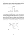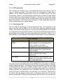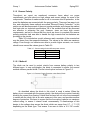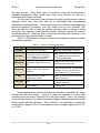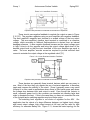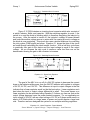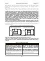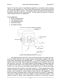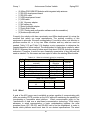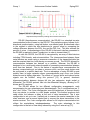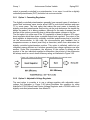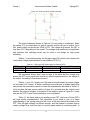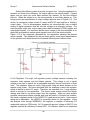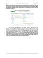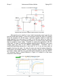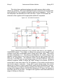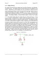
1
Autonomous
Surface Vehicle
Group #1
Team Members:
Michael Podel
Gor Beglaryan
Stanislaus Bernard
Christina Sylvia
April 29, 2011
Sponsored By:
Robotics Club at the University of Central
Florida
Group 1
Autonomous Surface Vehicle
Spring 2011
TABLE OF CONTENTS
1.
AUTONOMOUS SURFACE VEHICLE OVERVIEW .............................................................. 3
1.1
INTRODUCTION.................................................................................................................. 3
1.2
PURPOSE ......................................................................................................................... 3
TH
1.3
AUVSI AND ONR’S 4 INTERNATIONAL ASV COMPETITION................................................ 3
1.4
ASV OBJECTIVES 2011 .................................................................................................... 5
1.4.1 Electrical ..................................................................................................................... 5
1.4.2 Software ..................................................................................................................... 6
1.4.3 Mechanical ................................................................................................................. 6
2.
SPECIFICATIONS, BUDGET, AND TIMELINE ..................................................................... 6
2.1
TECHNICAL OBJECTIVES .................................................................................................... 7
2.1.1 Goals .......................................................................................................................... 7
2.2
BUDGET AND FINANCING ................................................................................................... 7
2.3
TIMELINE .......................................................................................................................... 8
2.4
TESTING SCHEDULE .......................................................................................................... 8
2.5
CONSULTANTS AND SUPPLIERS ......................................................................................... 9
2.5.1 ASV Team .................................................................................................................. 9
2.5.2 Advisors ...................................................................................................................... 9
2.5.3 Suppliers..................................................................................................................... 9
2.6
FACILITIES AND EQUIPMENT............................................................................................... 9
3.
RESEARCH .......................................................................................................................... 10
3.1
POWER........................................................................................................................... 10
3.1.1 Emergency Stop ....................................................................................................... 10
3.1.2 Reverse Polarity ....................................................................................................... 15
3.1.3 Hot Swapping ........................................................................................................... 18
3.1.4 Voltage Regulation ................................................................................................... 19
3.1.5 Voltage and Current Sensing ................................................................................... 26
3.2
MICROCONTROLLER ........................................................................................................ 33
3.2.1 What’s Needed ......................................................................................................... 33
3.2.2 Parts Researched ..................................................................................................... 35
3.2.3 Comparison of Microcontrollers................................................................................ 37
3.3
FIELD PROGRAMMABLE GATE ARRAY (FPGA).................................................................. 38
3.3.1 Background .............................................................................................................. 38
3.3.2 What’s Needed ......................................................................................................... 39
3.3.3 Part’s Research ........................................................................................................ 39
3.3.4 XC3S500E vs. EPF10K70........................................................................................ 40
3.4
COMMUNICATION ............................................................................................................ 41
3.4.1 Wireless .................................................................................................................... 42
3.4.2 Wired ........................................................................................................................ 47
3.5
SENSORS ....................................................................................................................... 53
3.5.1 Temperature / Humidity Sensors ............................................................................. 53
3.5.2 Light Sensor ............................................................................................................. 57
3.6
DYNAMIC FAN CONTROL.................................................................................................. 60
3.6.1 Option 1: Cascading Regulators .............................................................................. 61
3.6.2 Option 2: Adjustable Voltage Regulator ................................................................... 61
3.6.3 Option 3: Motor Controller ........................................................................................ 63
3.6.4 Option 4: Fan Controller IC (PWM Based) ............................................................... 63
3.6.5 Option 5: FET driven Fan ......................................................................................... 64
3.7
DISPLAYS ....................................................................................................................... 64
3.7.1 Liquid Crystal Display (LCD) .................................................................................... 65
3.7.2 Twisted Nematic (TN) [4] .......................................................................................... 65
3.7.3 Super Twisted Nematic (STN) [36] .......................................................................... 66
3.7.4 Thin-film-transistor (TFT) [4]..................................................................................... 66
iii
Group 1
3.7.5
3.7.6
3.7.7
4.
Autonomous Surface Vehicle
Spring 2011
In Plane Switching (IPS) [42].................................................................................... 67
Vertical Alignment (VA) [42] ..................................................................................... 67
Light Emitting Diode (LED) displays ......................................................................... 68
DESIGN ................................................................................................................................. 71
4.1
POWER........................................................................................................................... 71
4.1.1 Emergency Stop ....................................................................................................... 71
4.1.2 Reverse Polarity ....................................................................................................... 82
4.1.3 Hot Swapping ........................................................................................................... 83
4.1.4 Voltage Regulation ................................................................................................... 84
4.1.5 Voltage Sensing ....................................................................................................... 92
4.1.6 Current Sensing........................................................................................................ 93
4.2
MICROCONTROLLER ...................................................................................................... 100
4.2.1 Power ..................................................................................................................... 101
4.2.2 Two-Wire Interface ................................................................................................. 102
4.3
FPGA .......................................................................................................................... 104
4.3.1 PCB Design for the FPGA ...................................................................................... 104
4.3.2 Implementation of Asynchronous Serial ................................................................. 105
4.4
COMMUNICATION .......................................................................................................... 109
4.5
SENSORS ..................................................................................................................... 110
4.5.1 Temperature ........................................................................................................... 110
4.5.2 Light ........................................................................................................................ 112
4.6
DYNAMIC FAN CONTROL................................................................................................ 112
4.7
DISPLAYS ..................................................................................................................... 113
5.
BUILDING / TEST PROCEDURE ....................................................................................... 113
5.1
POWER......................................................................................................................... 114
5.1.1 Emergency Stop ..................................................................................................... 114
5.1.2 Reverse Polarity ..................................................................................................... 114
5.1.3 Hot Swapping ......................................................................................................... 114
5.1.4 Voltage Regulators ................................................................................................. 114
5.1.5 Voltage Sensing ..................................................................................................... 116
5.1.6 Current Sensing...................................................................................................... 117
5.2
MICROCONTROLLER ...................................................................................................... 118
5.2.1 Power and Signals ................................................................................................. 118
5.2.2 Software Check ...................................................................................................... 120
5.3
FIELD PROGRAMMABLE GATE ARRAY ............................................................................. 121
5.3.1 Power and Signals ................................................................................................. 121
5.3.2 Software Check ...................................................................................................... 121
5.4
COMMUNICATION .......................................................................................................... 121
5.4.1 Wireless Communication - XBee Test Procedure [5] ............................................. 121
5.5
SENSORS ..................................................................................................................... 124
5.5.1 Temperature Sensor (1-COTS) .............................................................................. 124
5.5.2 Temperature Sensor (2-Thermistor) ...................................................................... 125
5.5.3 Light ........................................................................................................................ 127
5.6
DYNAMIC FAN CONTROL................................................................................................ 128
5.7
DISPLAYS ..................................................................................................................... 129
6.
USER MANUAL .................................................................................................................. 129
6.1
TURNING ON THE ASV .................................................................................................. 129
6.1.1 Connect Batteries to the ASV................................................................................. 129
6.1.2 Connect Shore Power to the ASV .......................................................................... 130
6.1.3 Powering On with Batteries .................................................................................... 131
6.1.4 Powering On with Shore Power ............................................................................. 131
6.2
SWITCHING BETWEEN POWER SOURCES ....................................................................... 132
6.3
MONITORING ASV VITALS ............................................................................................. 132
iv
Group 1
Autonomous Surface Vehicle
Spring 2011
6.3.1 Description of LCD Screens ................................................................................... 133
6.3.2 Using the On-Board LCD Screen ........................................................................... 133
6.3.3 Using the Remote LCD Screen .............................................................................. 134
6.4
EMERGENCY STOP SYSTEM .......................................................................................... 135
6.4.1 Connecting the ESTOP Circuit ............................................................................... 135
6.4.2 Resetting the ESTOP Circuit .................................................................................. 136
6.4.3 Emergency Stopping the ESTOP Circuit ............................................................... 137
6.5
COMPUTER POWER....................................................................................................... 138
7.
EXPLICIT DESIGN SUMMARY .......................................................................................... 138
8.
BIBLIOGRAPHY ................................................................................................................. 140
A
SYSTEM DIAGRAMS ......................................................................................................... 143
A.1
A.2
A.3
A.4
PCB LAYOUT ................................................................................................................ 143
SHORE POWER ............................................................................................................. 143
POWER DISTRIBUTION ................................................................................................... 144
LOGIC DISTRIBUTION ..................................................................................................... 144
B
TIMELINE ............................................................................................................................ 145
C
COPYRIGHTS ..................................................................................................................... 146
Table of Figures
FIGURE 1.1 - COMPETITION MAP ......................................................................................................... 5
FIGURE 3.1 - ELECTROMECHANICAL RELAY OPERATION ..................................................................... 12
FIGURE 3.2 - SOLID STATE RELAY OPERATION ................................................................................... 12
FIGURE 3.3 - REVERSE POLARITY PROTECTION USING SERIES DIODE................................................. 15
FIGURE 3.4 - REVERSE POLARITY PROTECTION USING PARALLEL DIODE ............................................ 16
FIGURE 3.5 - REVERSE POLARITY PROTECTION USING P-FET ........................................................... 17
FIGURE 3.6 - FULL W AVE RECTIFIER (BATTERY POLARITY IS CORRECT) .............................................. 18
FIGURE 3.7 - FULL W AVE RECTIFIER (BATTERY POLARITY IS NOT CORRECT) ....................................... 18
FIGURE 3.8 - HOT SWAPPING CIRCUIT ............................................................................................... 19
FIGURE 3.9 - LINEAR BUCK CONVERTER............................................................................................ 23
FIGURE 3.10 - LINEAR REGULATOR NEGATIVE FEEDBACK .................................................................. 23
FIGURE 3.11 - SWITCHING BUCK CONVERTER ................................................................................... 25
FIGURE 3.12 - SWITCHING BOOST CONVERTER ................................................................................. 25
FIGURE 3.13 - HIGH VS. LOW SIDE CURRENT SENSE USING SHUNT RESISTOR ................................... 28
FIGURE 3.14 - HALL EFFECT DIAGRAM .............................................................................................. 30
FIGURE 3.15 - OPEN LOOP HALL EFFECT DIAGRAM ........................................................................... 31
FIGURE 3.16 - CLOSED LOOP HALL EFFECT DIAGRAM........................................................................ 32
FIGURE 3.17 - ILLUSTRATION OF LOGIC CELLS ................................................................................... 40
FIGURE 3.18 - UART DATA TRANSMIT FORMAT: 1 START BIT, 8 DATA BITS, 1 PARITY BIT, 1 STOP BITS. .. 45
FIGURE 3.19 - I2C MASTER/SLAVE CONFIGURATION .......................................................................... 49
FIGURE 3.20 - I2C DATA TRANSFER CONFIGURATION. ........................................................................ 50
FIGURE 3.21 - RS-232 DATA CHARACTERISTICS. ............................................................................... 51
FIGURE 3.22 - BLOCK DIAGRAM OF WIRED COMMUNICATION PLATFORM, .............................................. 53
FIGURE 3.23 - CONDITIONING SIGNAL PATH ....................................................................................... 56
FIGURE 3.24 - BLOCK DIAGRAM ......................................................................................................... 59
FIGURE 3.25 - SETUP OF THE FIRST SCENARIO WITH THE EFFICIENCY FOR A CASCADE SETUP ............... 61
FIGURE 3.26 - BASIC SETUP OF AN ADJUSTABLE VOLTAGE REGULATOR ............................................... 62
FIGURE 3.27 - A MORE SPECIFIC VERSION OF THE ADJUSTABLE VOLTAGE REGULATOR ......................... 62
FIGURE 3.28 - MICREL’S MIC502 SETUP TO DETERMINE [28] ............................................................. 63
FIGURE 3.29 - CELL OF TN LCD DISPLAY. ......................................................................................... 66
FIGURE 3.30 - TFT TECHNOLOGY...................................................................................................... 67
FIGURE 3.31 - LCD DISPLAY............................................................................................................. 70
v
Group 1
Autonomous Surface Vehicle
Spring 2011
FIGURE 4.1 - ACTIVE E-STOP CIRCUIT-1 ........................................................................................... 74
FIGURE 4.2 - POLOLU MODULE FOR E-STOP CIRCUIT......................................................................... 75
FIGURE 4.3 - POLOLU RC SWITCH WITH DIGITAL OUTPUT ................................................................... 75
FIGURE 4.4 - HIGH CURRENT DC SWITCH .......................................................................................... 76
FIGURE 4.5 - HIGH CURRENT DC SWITCH SCHEMATIC ........................................................................ 77
FIGURE 4.6 - HIGH CURRENT DC SWITCH SIMULATION ........................................................................ 78
FIGURE 4.7 - PASSIVE E-STOP CIRCUIT SCHEMATIC ........................................................................... 79
FIGURE 4.8 - PASSIVE E-STOP INCLUDING EXTERNAL RELAYS............................................................. 81
FIGURE 4.9 - SCHEMATIC FOR PASSIVE E-STOP CIRCUIT ................................................................... 82
FIGURE 4.10 - SCHEMATIC OF “REVERSE POLARITY PROTECTION” ..................................................... 83
FIGURE 4.11 - "HOT SWAPPING" CIRCUIT SCHEMATIC ........................................................................ 84
FIGURE 4.12 - 5V LM2676 CHARACTERISTIC CHARTS ....................................................................... 85
FIGURE 4.13 - 5V LM2676 SCHEMATIC ............................................................................................. 86
FIGURE 4.14 - 8V LM2675 CHARACTERISTIC CHARTS ....................................................................... 87
FIGURE 4.15 - 8V LM2675 SCHEMATIC ............................................................................................. 88
FIGURE 4.16 - 8V LM2676 CHARACTERISTIC CHARTS ....................................................................... 88
FIGURE 4.17 - 12V LM22677 CHARACTERISTIC CHARTS ................................................................... 89
FIGURE 4.18 - 12V LM22677 SCHEMATIC......................................................................................... 90
FIGURE 4.19 - PTN78020W CHARACTERISTIC CHARTS..................................................................... 91
FIGURE 4.20 - 12V PTN78020W SCHEMATIC ................................................................................... 91
FIGURE 4.21 - VOLTAGE SENSING ..................................................................................................... 92
FIGURE 4.22 - SENSE RESISTOR CIRCUIT .......................................................................................... 95
FIGURE 4.23 - CURRENT SENSE MAX9920 ....................................................................................... 96
FIGURE 4.24 - LEM LAH 25-NP DIMENSIONS ................................................................................... 97
FIGURE 4.25 - LEM LAH 25-NP SCHEMATIC..................................................................................... 99
FIGURE 4.26 - LEM LTS 15-NP SIZE ................................................................................................ 99
FIGURE 4.27 - LEM LTS 15-NP SCHEMATIC ................................................................................... 100
FIGURE 4.28 - ILLUSTRATION OF SCHEMATIC AND BOARD LAYOUT FOR THE MICROCONTROLLER
REGARDING POWER ............................................................................................................... 101
FIGURE 4.29 - PROGRAM FLOW FOR A TWO-W IRE INTERFACE [14] ................................................... 103
FIGURE 4.30 - ILLUSTRATION OF THE HARDWARE SETUP NEEDED FOR A TWO-WIRE INTERFACE........... 103
FIGURE 4.31 - FOOTPRINT OF THE XILINX SPARTAN3E ..................................................................... 104
FIGURE 4.32 - SAMPLING THE DATA STREAM FROM THE RECEIVER .................................................... 106
FIGURE 4.33 - FLOW FOR DATA ON THE RECEIVING UART AT 16 TIMES THE BAUD RATE ..................... 108
FIGURE 4.34 - XBEE WIRELESS SCHEMATIC ..................................................................................... 109
FIGURE 4.35 – DS18S20 TEMPERATURE SENSOR SCHEMATIC ......................................................... 110
FIGURE 4.36 - THERMISTOR TEMPERATURE SENSOR SCHEMATIC ...................................................... 111
FIGURE 4.37 - DISPLAY, SWITCH, MICROCONTROLLER CONNECTION ................................................ 113
FIGURE 5.1 - 5V LM2676 EAGLE SCHEMATIC .................................................................................. 115
FIGURE 5.2 - 8V LM2676 EAGLE SCHEMATIC .................................................................................. 116
FIGURE 5.3 - 12V LM22677 EAGLE SCHEMATIC .............................................................................. 116
FIGURE 5.4 - MAX9920 SCHEMATIC ............................................................................................... 118
FIGURE 5.5 - X-CTU PROGRAM ...................................................................................................... 123
FIGURE 5.6 - X-CTU RANGE TEST .................................................................................................. 124
FIGURE 6.1 - 4 CELL BATTERY ........................................................................................................ 129
FIGURE 6.2 - 6 CELL BATTERY ........................................................................................................ 129
FIGURE 6.3 - BOX SWITCHES .......................................................................................................... 130
FIGURE 6.4 - RELAY SWITCH........................................................................................................... 130
FIGURE 6.5 - RHINO SHORE SUPPLY ............................................................................................. 131
FIGURE 6.6 - SHORE POWER CABLE................................................................................................ 131
FIGURE 6.7 - MAIN LCD SCREEN .................................................................................................... 134
FIGURE 6.8 - REMOTE LCD SCREEN ............................................................................................... 135
FIGURE 6.9 - EXTERNAL ESTOP BUTTON ....................................................................................... 135
FIGURE 6.10 - FUTABA TRANSMITTER ........................................................................................... 136
FIGURE 6.11 - FUTABA ESTOP SWITCH ....................................................................................... 136
FIGURE 6.12 - POLOLU RC SWITCH .............................................................................................. 137
vi
Group 1
Autonomous Surface Vehicle
Spring 2011
FIGURE 6.13 - RESET BUTTON ...................................................................................................... 137
FIGURE 7.1 - SYSTEM OVERVIEW .................................................................................................... 139
vii
Group 1
Autonomous Surface Vehicle
Spring 2011
Table of Tables
TABLE 1.1 - COMPETITION CHALLENGES .............................................................................................. 4
TABLE 2.1 - PROJECT COST ................................................................................................................ 8
TABLE 3.1 - FEATURES THAT MUST BE CONSIDERED BEFORE BUYING RELAYS ...................................... 11
TABLE 3.2 - SUMMARY OF RELAY CONTACT ARRANGEMENTS ............................................................. 11
TABLE 3.3 - RELAY SUMMARY: DIFFERENT TECHNOLOGIES, THEIR ADVANTAGES AND DISADVANTAGES.. 13
TABLE 3.4 - MINIMUM CURRENT/VOLTAGE REQUIREMENTS THAT MUST BE PROVIDED BY THE RELAYS .... 14
TABLE 3.5 - CURRENT RATINGS FOR THE DIFFERENT POWER SOURCES ............................................... 15
TABLE 3.6 - VOLTAGE REGULATION REQUIREMENTS .......................................................................... 21
TABLE 3.7 - LINEAR VS. SWITCHING REGULATORS ............................................................................. 22
TABLE 3.8 - HIGH SIDE CURRENT SENSING ....................................................................................... 28
TABLE 3.9 - LOW SIDE CURRENT SENSING ........................................................................................ 29
TABLE 3.10 - CURRENT SENSE METHOD COMPARISON ...................................................................... 33
TABLE 3.11 - COMPARISON OF ALL THE MICROCONTROLLERS STUDIED................................................ 38
TABLE 3.12 - COMPARISON BETWEEN THE FPGAS CONSIDERED ........................................................ 41
TABLE 3.13 - XBEE KIT INDIVIDUALLY PRICED FOR COMPARISON ......................................................... 47
TABLE 3.14 - PRICE COMPARISON ..................................................................................................... 47
TABLE 3.15 - RS-232 & RS-485 COMPARISON SUMMARY .................................................................. 52
TABLE 3.16 - HUMIDITY/TEMPERATURE SENSOR COST COMPARISON ................................................... 57
TABLE 3.17 - LIGHT SENSOR COST COMPARISON .............................................................................. 59
TABLE 3.18 - GENERAL DISPLAY SPECIFICATIONS .............................................................................. 68
TABLE 3.19 - LCD VS. LED .............................................................................................................. 69
TABLE 3.20 - LCD DISPLAY DETAILS ................................................................................................. 70
TABLE 4.1 - HIGH CURRENT DC SWITCH SPECS FOR DIFFERENT FETS ................................................ 77
TABLE 4.2 - SENSE RESISTORS LTC4151 ......................................................................................... 94
TABLE 4.3 - SENSE RESISTORS MAX9920 ........................................................................................ 97
TABLE 4.4 - CLOSED LOOP PCB CONFIGURATION.............................................................................. 98
TABLE 4.5 - ILLUSTRATION OF THE DATA SENT FOR A GIVEN PACKET .................................................. 105
TABLE 4.6 - ADDRESS PINS AND SLAVE ADDRESSES FOR THE TMP100 ............................................. 110
Table of Equations
EQUATION 3.1 - BOOST GAIN EQUATION............................................................................................ 25
EQUATION 3.2 - LINEAR REGULATOR - POWER W ASTED ..................................................................... 25
EQUATION 3.3 - PULL-UP RESISTOR EQUATION FOR I2C BUS............................................................... 49
EQUATION 3.4 - EQUATION FOR RELATIONSHIP BETWEEN CAPACITANCE AND FREQUENCY .................... 63
EQUATION 4.1 - SENSE RESISTOR SCALING LTC4151 ....................................................................... 93
EQUATION 4.2 - MAX9920 GAIN FORMULA ....................................................................................... 96
EQUATION 4.3 - LEM LTS 15-NP FORMULA .................................................................................... 100
EQUATION 4.4 - SWITCHING FREQUENCY......................................................................................... 101
EQUATION 4.5 - NUMBER OF SAMPLES ............................................................................................ 107
EQUATION 4.6 - SAMPLING PER CLOCK PULSE .................................................................................. 107
viii
Group 1
Autonomous Surface Vehicle
Spring 2011
Executive Summary
Every summer the Association for Unmanned Vehicle Systems International
(AUVSI) hosts the Autonomous Surface Vehicle (ASV) competition. The Robotics
Club at the University of Central Florida (UCF) annually participates in this
competition which involves engineering a fully autonomous vehicle to perform the
challenges set forth by AUVSI. This encompasses using students of all disciplines
to create an innovative, efficient, and ergonomic platform for competition. Our senior
design team, composed of electrical engineers, has come together to engineer the
electronics portion of the ASV. This includes power regulation/distribution, power
monitoring, vehicle safety, on-board and remote monitoring of system for vitals, and
processing of some sensor data.
Power regulation will efficiently control and distribute regulated and
unregulated voltage throughout the vehicle for its onboard systems. This involves
controlling three input sources as well as seamlessly hot swapping between two of
these input sources. The vehicle will have protection from accidental input source
reverse polarity as well as excess current draw. Our goal this year is to monitor all
the vitals of our system including input source voltages, input source current draw,
temperature, and humidity. We will have the ability to monitor the vitals through the
on-board computer, on-board LCD screen, as well as a remote LCD screen.
The ASV is comprised of numerous sensors which include multiple vision
systems, a compass, a global positioning system (GPS), LIDAR, light, current,
temperature, humidity, and mechanical feedback. These systems are integrated in
the vehicle by using multiple devices over several communication protocols. The
processing power on the ASV consists of a computer, a field programmable gate
array (FPGA), and a microcontroller. They utilize USB, serial, and I2C to
communicate between each other and share information gathered from sensors. All
vision and some sensor processing is handled by the computer, which in turn directs
the FPGA to send signals to motors/thrusters and other mechanical devices on the
vehicle. In response to these signals the vehicle moves and performs specific tasks
necessary for completing the overall competition.
In order to provide a more detailed diagnostic of the current condition of the
ASV, light and temperature sensors have been selected to aid in achieving the
utmost control over the ASV. The light sensor has been designed to assist in color
identification of objects. The set of four light sensors, composing the light detection
assembly pack, each occupy a different navigational direction. They will interpret the
amount of ambient light available and send this information to the microcontroller
where it can then be determined where the light is coming from and if it could be
affecting the “true” color of the object of interest. The temperature sensors will
dictate whether the electrical boxes are creating too much heat for the electrical
components inside to work efficiently. The temperature obtained from these
readings will then be used to control the fan speed inside the ASV electrical box.
Our senior design team in conjunction with the Robotics Club have decided that
being able to display the diagnostic current conditions of the ASV will be
accomplished both through an on board LCD display and via remote. To realize this
1
Group 1
Autonomous Surface Vehicle
Spring 2011
task we have selected to utilize ZigBee’s XBee Pro wireless modules. This form of
wireless communication has proven to satisfy all of our core requirements in addition
to exceeding our desired range of 900 ft.; while requiring a sufficiently small amount
of power in the process.
In order to maintain a high level of safety as we work with both high voltages and
high currents various layers of safety protection will be implemented. One such
protection is the inclusion of an emergency stop circuit. As per competition rules,
the ASV must have included in its design a method in which all power can be cut
from any moveable parts on board. The E-Stop circuit we will design will be capable
of cutting power to these moveable parts in three locations. Two locations will be
located directly on the ASV and a third will be accessible via remote. After
considering the pros and cons of the E-Stop circuit from previous years we have
decided to implement an emergency stop circuit that does not require any logic
components. The exclusion of logic components should offer better protection, and
allow the system to be in E-Stop mode when initial power is applied to the ASV. The
E-Stop circuit is designed to operate using set and reset buttons. The reset button
for our design purposes will only be accessible on board. Another measure of safety
protection that we will be implementing is reverse polarity protection. When an input
source is connected with the wrong polarity, the circuit will ensure that the
electronics of the ASV are protected from any harmful side effects.
2
Group 1
Autonomous Surface Vehicle
Spring 2011
1. Autonomous Surface Vehicle Overview
1.1 Introduction
The purpose of this project is to engineer an electrical integration system necessary
for an autonomous surface vehicle (ASV) to compete in competition. Integration
involves power distribution and monitoring, sensor monitoring, and communication.
This project involves knowledge and implementation of electrical and computer
engineering. The integration includes using analog and digital hardware along with
programming to interpret sensor information and relay it to the proper devices in the
system.
1.2 Purpose
The Association for Unmanned Vehicle Systems International (AUVSI) and ONR
(Office of Naval Research) hosts several autonomous robotics competitions each
year for students to participate in. Besides our autonomous surface vehicle
competition, AUVSI also hosts competitions for ground, underwater, and aerial
environments. These competitions give students the opportunity to work together
with other students in multiple disciplines to engineer unmanned vehicles. With a
new set of rules every year, the teams must devise a plan to engineer their
autonomous vehicle to meet the specifications and requirements set forth by the
competition. Fortunately, the Robotics Club at UCF has the ability to participate in
many of these competitions which are incredible learning experiences for all the
students involved. The club has participated in the last three ASV competitions with
great success. This year the ASV team has again decided to upgrade the electrical
system for a more efficient and technologically advanced system.
1.3 AUVSI and ONR’s 4th International ASV Competition
AUVSI and ONR host the international ASV competition for students to gain
knowledge and to participate in. For the past two years including this year, the
competition has been held at The Founder’s Inn and Spa in Virginia Beach, Virginia.
This facility generously hosts the competition for around ten to fifteen teams. The
Inn has a large lake in the back of the property where the competition is held along
with tents for each team and the judges. From June 9th through the 12th the teams
will compete and have several opportunities to gain points though static judging,
qualifier runs, and the final competition. The static judging consists of judges
reviewing the teams’ paper, website, t-shirts, and overall oral presentation. From the
rankings of the static judging, the teams will choose the time in which they will have
their two qualifying runs. From the points in the qualifying runs, the teams that make
it though qualifying will choose their times for the final competition. AUVSI sends out
a set of rules about seven months before competition which describes the
challenges and the rules for the upcoming competition. The teams then take these
rules and engineer a vehicle that can meet the competitions challenges.
3
Group 1
Autonomous Surface Vehicle
Spring 2011
The rules list the specifications including the size, weight, and other areas in
which the vehicle must adhere to. For the AUVSI competition, the ASV’s are limited
to a vehicle which is three feet high, three feet wide, and six feet long and must
weigh within certain limits. If the vehicle is lighter the vehicle is awarded points and
if the vehicle is overweight, the vehicle looses points. This is done to ensure that the
vehicles can compete together and that competitors don’t build vehicles that are to
large or heavy and create an unfair advantage compared to other teams. The final
section of the rules specifies information about point distribution/weight as well as
the specifications of the obstacles used in the course.
This year’s
missions/challenges can be found in Table 1.1.
Table 1.1 - Competition Challenges
Thrust Test
Speed Test
Navigate out
of the harbor
The
Challenge
Stations
Return to the
dock
Tests the thrust of the vehicle using the vehicles motors at full power
Vehicle must pass through two gates with the first gate about 15-30 feet
from the dock and the second gate about 50-100 feet away from the first
gate. Each gate is about six feet apart from each other.
This challenge requires navigating about a dozen sets of navigational
buoys with some obstacles in their way.
(Earth) Amphibious Landing:
The vehicle will need to be amphibious itself or devise a way to deploy
another vehicle in order to retrieve an object on a landing zone out of the
water.
(Fire) Find the fire and extinguish it:
The ASV needs to locate a ship with a red cutout in it and spray water
into the cutout until the fire is out which is designated by something
changing on the ship.
(Air) Find and report the ‘hot’ target:
The ASV will locate a set of four targets, determine which target is the
hottest and report its GPS location back to the base station.
(Water) Turn off the waterfall:
The ASV will locate a waterfall, go through the waterfall, and find a
button to shutdown the waterfall.
After all missions have been completed, the ASV will navigate back
through the harbor to the starting dock.
Figure 1.1 shows the layout of the competition for this year’s challenges. The
course is divided into two almost identical courses which will most likely be used as
a practice course and another for the actual competition. Starting from the dock you
have the speed test though the gates followed by the navigational challenge. After
that you can perform as many of the other challenges as you can before returning to
the dock again within the 20 minute time period.
4
Group 1
Autonomous Surface Vehicle
Spring 2011
Figure 1.1 - Competition Map
Reprinted with permission from AUVSI
1.4 ASV Objectives 2011
Our overall objective for the ASV is to improve on last year’s performance. Although
we have performed extremely well over the past three competitions, there is still
always room for improvement. This year the electrical has improved on the overall
efficiency of the vehicle as well as improved on our integration and feedback
systems. This means we can test longer with fewer interruptions for electrical
worries.
1.4.1 Electrical
The electrical system has been redesigned this year to house a power grid that runs
as a nominal 24V DC system. This year’s focus has been to make the entire system
more efficient by reducing standby current and focusing power distribution to the
components that are essential to the vehicles operation; any other device has the
5
Group 1
Autonomous Surface Vehicle
Spring 2011
ability to either be turned off or have its power throttled to a minimum. The power
board has enhanced capabilities this year ranging from hot-swapping input sources,
reverse polarity protection and many other features that help protect the board from
unforeseen accidents. We have incorporated light sensors on board to help
determine the location of the sun in order to facilitate the vision recognition system.
There is a dynamic fan control system that varies the fan speed according to the
temperature of the main box in an effort to maintain an optimal operating
temperature for maximum efficiency.
1.4.2 Software
From a top view, this project has two different levels of programming; one level
consists of the high level decision maker executing code from a high end computer
running a debian based Linux operating system. The lower level software consists of
hardware-based programming and this code is executed using a network of a single
FPGA with multiple microcontrollers; they will control basic motor control and sensor
integration. The higher level programming uses the Joint Architecture for Unmanned
Systems (JAUS) format as its base structure and thus all communication with
devices linked with the on-board decision engine also follows a subset of the JAUS
standard. This subset of JAUS is governed by the Robotics Club at UCF. As this
design project only encompass the electronics aspect of the Autonomous Surface
Vehicle, only the hardware based programming is within the scope of this project.
1.4.3 Mechanical
This year’s ASV will undergo a few mechanical design modifications. Attentively,
these changes include new hulls, and a wider frame used to connect the hulls. This
wider frame will reduce the amount of wobbling the ASV has demonstrated when on
the water. In addition to these changes the ASV has obtained a new motor box, and
a new electrical box. These boxes are mounted side by side occupying the same
general space as in previous years. To extend the ASV’s capabilities Crust Crawler
Motors have been added for enhanced propulsion. These motors are water cooled
to protect them from overheating. Of the three motors, there is a center motor which
has the ability to rotate 90o so that it can be used as a forward motor as well as a
lateral motor for added maneuverability.
2. Specifications, Budget, and Timeline
This section is used to specify the requirements of the Senior Design team to meet
the requirements set forth with the ASV team. We are continuously looking to
improve the vehicle to make sure we have a competitive edge at competition both
with the actual in water competition as well as in the static judging of the ASV.
Below will describe the current objectives, budget, timeline for the team, testing
goals, and assistance from the Robotics Club.
6
Group 1
Autonomous Surface Vehicle
Spring 2011
2.1 Technical Objectives
This year we have strived to achieve a greater vehicle that will meet a new set of
specifications. We have acquired these specifications from the AUVSI competition
rules as well as the needs of the ASV team. The senior design team has met these
goals to the best of their ability.
•
•
•
•
•
•
•
•
•
Nominally operate using 6-cell lithium-polymer batteries at 22.2V DC
Distribute power with an efficiency of 85% or greater
Monitor all power sources voltage and current with an accuracy of ±1.0%
Integrate all vehicle electronics onto a printed circuit board (PCB) for routing
to the appropriate devices and components
Seamlessly switch from shore power to battery power
Implement vehicle safety including an emergency stop system to physically
disconnect power to all moving parts
Monitor vehicle temperature and humidity
Implement a wireless platform to allow feedback via remote
Receive visual feedback from an onboard and remote display
2.1.1 Goals
The following list describes the goals the senior design team has implemented for
the ASV team:
•
•
•
•
•
•
•
Provide an ergonomic system for easy assembly and disassembly of
electrical components
Provide necessary information for communication protocols between devices
Allow calibration of voltage sensing
Add test points on PCB for easy troubleshooting
Label all parts on the PCB for easy troubleshooting
Generate temperature and ambient light sensing
Provide necessary wireless communication to receive ASV vitals via remote
2.2 Budget and Financing
This project is completely and generously financed by the Robotics Club at UCF in
conjunction with their sponsors. The ASV itself has made two major purchases
including a new set of thrusters with a spare motor ($3,500), and a new computer
($1,000). In addition to this the ASV has ordered two PCBs fully populated
($500.00), a modified hull, and new sensors. We have allocated $5,500.00 for the
overall vehicle this year which does not include the cost of traveling to Virginia. We
have reused many sensors and devices from last year to reduce the cost of the
vehicle including cameras, compass, GPS, LIDAR, and FPGA. Table 2.1 is a more
detailed table containing the vehicles components.
7
Group 1
Autonomous Surface Vehicle
Spring 2011
Table 2.1 - Project Cost
ITEM
FINANCE
FPGA
LIDAR
ASV Team
Lockheed
Martin
Stereo Vision
Lockheed
Martin
GPS
ASV Team
Camera
ASV Team
Unibrain
ASV Team
Compass
ASV Team
Subtotal (Already Purchased)
LIDAR
Sponsorship
HD Webcam
ASV Team
ASV Computer
Sponsorship
Microcontroller (X2)
ASV Team
LCD Screens (X2)
ASV Team
ZigBee Pro
ASV Team
PCB Components
ASV Team
(X2)
Pelican Case
ASV Team
Connectors
ASV Team
Mechanical
ASV Team
Subtotal (New Costs)
Total Cost
APPROXIMATE
COST
$150
$5,590
$3,000
$1,500
$700
$100
$1,500
$12,540
$3,950
$100
$1,000
$20
$60
$150
$500
$100
$100
$500
$6,480
$19,020
2.3 Timeline
A milestone chart has been created in Appendix B which describes the way our
project was distributed between our group members. We tried to distribute the work
according to our preferences and at the same time we tried to ensure that all of us
have approximately the same amount of research to do. The research portion of the
project was the most time consuming part, which can be seen in the Gantt chart.
Our work was divided into three phases or stages as shown in the chart. The first
stage is the research stage followed by the circuit design stage. Each of us
completed our sections by creating the schematics, which was the final stage of our
work. All this can be seen in the chart.
2.4 Testing Schedule
Design of such systems for our vehicle requires good planning and testing. This
was the main subject for the second semester. We began the second semester by
building and testing each subsystem to confirm they perform as intended. After
completing this successfully, we combined all the subsystems and made sure our
overall system works as planned. Some unexpected results have occurred;
therefore we had to change portions of the design and repeat the testing and tuning
procedure until the desired outcome was achieved.
8
Group 1
Autonomous Surface Vehicle
Spring 2011
2.5 Consultants and Suppliers
The following few sections describe the consultants and suppliers that our senior
design team and ASV team have worked with throughout the scope of this project.
They included academic advisors and mentors from the university and various
companies.
2.5.1 ASV Team
Our senior design group was composed of four members; two of the four members
were part of the robotics club in previous years, and have remained active members
of the ASV team. With the aid of previous experience our senior design group was
better capable of integrating the desired design and testing techniques needed to
realize a more robust ASV.
2.5.2 Advisors
The two main advisors will be Gary Stein and the robotics club academic advisor
Daniel Barber. Both advisors are previous members of the robotics club and have a
vast array of robotic competition experience. With the support of these advisors our
group will remain on schedule and overcome any hurdles that may be presented to
us.
2.5.3 Suppliers
To accommodate our design requirements many suppliers were used to supply the
vast array of components that were utilized. Our specific design required the
purchase of a FPGA board, microcontroller, various sensors, and etc devices. To
account for the accruing financial cost, the ASV team used the existing sponsorships
from Lockheed Martin, as well as the Institute for Simulation and Training (IST) and
U.S. Army Research, Development, and Engineering Command (RDECOM).
2.6 Facilities and Equipment
Another benefit of having membership in the Robotics Club is the access to the
Robotics Lab. Our lab is located in the Partnership II building on Research Parkway.
The lab space is quite large and houses all the club’s projects including the IEEE,
ground, sub, and surface vehicles. The lab is also equipped with a machine shop,
electronics workbench, and storage for the vehicle and its related parts.
The electronics workbench is where most of our work was performed. It houses our
power supplies, oscilloscopes, function generators, and soldering stations. In
addition to this, the club has a variety of tools for crimping, stripping, and cutting
wire. A vast array of wire types and sizes are also available along with electrical
components ranging from passive components to many active components. This
saved us from making many trips out to stores for supplies.
9
Group 1
Autonomous Surface Vehicle
Spring 2011
3. Research
3.1 Power
3.1.1 Emergency Stop
One of the competition rules for this project is to have E-Stop functionality. This
feature will be triggered by multiple E-Stop buttons on the boat, and also remotely.
Even if this feature had not been a part of the requirements, any such scale design,
with this many features and devices connected would have an E-Stop functionality.
This would be triggered under certain conditions to prevent the circuit boards and
the connected devices from damage. It’s important to note that equipment protection
comes after human protection, which is also provided by the E-Stop circuit. By
designing this circuit, we assumed that the E-Stop circuit will be used very
frequently; therefore it is in a location visible to everyone. For that purpose our EStop trigger is a big, red button. The operator has access to an E-Stop button
anytime, which enables him/her to trigger it in an event that the vehicle is out of the
water, or in case of danger or emergency. Taking this into consideration we have
designed such a circuit. Our E-stop circuit can be triggered by 3 buttons, and also
wirelessly. There are quite a few E-Stop designs that we considered, however, all
the designs have one device, the relay, in common. The relay is the most important
and crucial component of this circuit. When there’s current through the relay and the
circuit is complete, our motor controllers and motors are powered. In this state the
relay must be able to provide the necessary current to meet the load needs. In the
case when the E-stop is triggered any power needs to be cutoff and our motor
controllers and motors need to be completely turned off. In addition to desired
performance we need to consider efficiency and cost.
The great abundance of relays and applications in which they are used,
makes it very difficult to choose a relay. However, we simplify this issue by
considering some key factors and features that one must consider when looking for
a relay. These factors and features are summarized in Table 3.1.
10
Group 1
Autonomous Surface Vehicle
Spring 2011
Table 3.1 - Features that must be considered before buying relays
Factor
Cost
Power
requirements
Switching
Contact
arrangement
Switch
contact
arrangement
Mounting
type
Specification
As low as possible for the given specs.
How will the relay be powered, AC or DC? How much power
will the relay dissipate?
At what voltage is the current being switched? How much
current is being switched? How much total current can the
relay handle?
Are we going to use type A, type B, or type C contact
arrangement relays (explained later in this report)?
Is the relay of choice going to be: “single pole changeover
(SPCO)”, or “double pole changeover (DPCO)”? How many
poles will the relay have, are we going to use a separate
relay for each motor controller, or we can purchase a multipole relay.
This includes surface mount, printed circuit board (PCB)
mount, plug-in socket, top mount, top-mount PCB, etc.
One very important technical aspect of a relay is the contact arrangement.
Relays are available in three different contact arrangements. These arrangements
and their operational specifications are given in Table 3.2.
Table 3.2 - Summary of Relay Contact Arrangements
Form
A
B
C
Description
This is the normally open (NO) arrangement, which means that the
switch is open when the coil is not energized, and it’s closed when
the coil is energized.
This arrangement is known as normally closed (NC). When the coil
is not energized the switch is closed, and the switch is open when
the coil is energized.
This arrangement is a combination of the first two types.
The contact arrangement has been chosen based on our needs. Another
factor that one must consider before buying a relay is the technology. Here we have
considered 4 widely used technologies.
3.1.1.1 Electromechanical Relay (EMR) [30]
The first relay we looked into was the electromechanical relay. This device is mainly
mechanical. A voltage is applied to the coil of the relay. If enough voltage is applied
to the coil the core of the relay magnetizes and pulls the arm towards it. This action
connects the two sides of the contacts to establish a connection as illustrated in
Figure 3.1. The electromechanical relay has many advantages; it’s very cheap,
readily available, it’s robust, and bulky, which we associate with reliability. The EMR
is a cool working device and doesn’t need a heat sink. Another great feature is that
electromechanical relays are also available in multiple poles, which may reduce
11
Group 1
Autonomous Surface Vehicle
Spring 2011
space requirements. However, it’s important to mention the fact that EMRs are big
and can create difficulties to mount on PCBs, especially when space is limited. Other
disadvantages include relatively slow switching speed and loud switching.
Figure 3.1 - Electromechanical Relay Operation
Reprinted with permission from National Instruments
3.1.1.2 Solid state relay (SSR) [30]
The solid state relay is another widely used relay. This device is based on transistor
technology, which is not mechanical. The operation technique of the SSR can be
summarized as follows: an input voltage is applied to an LED. The light of the LED is
reflected within an optical dome onto an array of photo diodes. The photo diodes
generate voltage which through some circuitry is used to control the gates of two
MOSFETs. A picture that makes this clear is shown in Figure 3.2. Advantages of the
SSR include low noise operation, virtually unlimited switching, small size, small ON
resistance, approximately zero output attenuation, etc. All the factors mentioned
above must be taken into consideration when buying a relay. One drawback of the
SSR is that price and size increase proportionally with higher performance.
Figure 3.2 - Solid State Relay operation
Reprinted with permission from National Instruments
12
Group 1
Autonomous Surface Vehicle
Spring 2011
3.1.1.3 FET switch [30]
FET switches are another type of non-mechanical devices that can be used as
relays to switch high loads. This device has all the advantages of SSRs and in
addition, it’s the fastest switching device, and can be smaller than all the other
technologies. However, one disadvantage is that this device doesn’t provide voltage
isolation, which may create hazardous situations. This device is not a likely choice
for our E-Stop circuit, since it doesn’t provide isolation from the voltage. This would
defeat the purpose of the E-Stop circuit. However, in small voltage applications this
device is ideal because of its great features.
3.1.1.4 Reed relays [30]
The reed relay is another type of electromechanical relay. The advantage of this
relay in contrast with the EMR is the 10 times faster switching speed and longer
lifetime. This devise may be useful for our low power switching needs, but it’s almost
of no practical use for high power operation, since the thin and small contacts melt at
high voltages and currents, and may permanently weld the switch. Table 3.3 is a
brief summary of all the different technologies and their details for quick referencing.
Table 3.3 - Relay summary: Different technologies, their advantages and disadvantages
Relay Summary
Technology
Electromechanical Relay
(EMR)
Solid State Relay (SSR)
Reed Relay
FET switch
Properties
Cheap, no heat sink necessary, multiple
poles available, 5-15 ms switching time,
robust, available in all contact
arrangements, relatively big in size.
Very fast switching, very long life time,
relatively small in size, cheap, heat sink
may be needed.
Small, fast, longer lifetime relative to the
EMR, not ideal for high voltage
applications.
Fastest switching, very long lifetime, very
small in size, no isolation, hence good for
low voltage applications.
As we can see relays have many specifications that must be identified.
Considering these technical information we identified our needs based on which we
chose an appropriate relay. The devices that are being turned off as soon as E-Stop
is de-energized are three Crust Crawler thrusters used to propel the boat (20A
each), a water pump (1A), that is used for providing water to the motor controllers for
cooling purposes, two Sabertooth motor controllers (20A max each), two servo
motors (1A each); in addition there is an extra relay, or an extra pole. The thruster is
the device with the biggest power rating. At maximum thrust and 24 volts this
devices is rated 400 W. Simple calculation shows that the relay of our choice has to
13
Group 1
Autonomous Surface Vehicle
Spring 2011
handle at least 16.67 amps at 24 volts. However, the batteries will not be able to
supply constant 24 volts, which could cause current variations. Taking this into
consideration, the relay of our choice must be able to switch 25 A. All the other
devices have power ratings that are considerably less than the thruster rating;
therefore we should be able to use multi pole 25 A relays. As outlined above, we
need at least 6 relays. We can use two 4 pole relays, or a single relay with at least 7
poles, to ensure we have at least one spare. All the requirements mentioned above
and other specifications are given in Table 3.4.
Table 3.4 - Minimum current/voltage requirements that must be provided by the relays
Feature
Component
Count
Cost
Coil Power
requirement
Contact power
Requirement
Contact
arrangement
Poles
Mounting type
Relay Requirements and Specifications
Sabertooth Motor
Crust Crawler
Water Pump
Controller
3
Less than
$100.00 per
relay
12V DC
powered
Switches at
24V, at least
60A total
Form A
(Normally
Open)
Capable of
handling 60 A,
either multiple
poles with low
current rating,
or single pole,
with at least
60A rating
Chassis mount,
panel mount,
socket
1
2
Less than
Less than
$100.00 per
$100.00 per relay
relay
12V DC
12V DC powered
powered
Switches at
Switches at 24V,
12V, at least
at least 40A total
2A
Form A
Form A (Normally
(Normally
Open)
Open)
Capable of
handling 2A
Chassis
mount,
panel
mount,
socket
14
Servo
Motors
2
Less than
$100.00
per relay
12V DC
powered
Switches
at 5V, at
least 1A
Form A
(Normally
Open)
Capable of
handling 40 A,
either multiple
Capable of
poles with low
handling
current rating, or
1A,
single pole, with
at least 40A rating
Chassis mount,
panel mount,
socket
Chassis
mount,
panel
mount,
socket
Group 1
Autonomous Surface Vehicle
Spring 2011
3.1.2 Reverse Polarity
Throughout our report we mentioned numerous times about our power
requirements, and also about our high voltage and current ratings for some of the
components. Therefore it makes sense for us to use some kind of protection, in the
event the batteries are connected with the wrong polarity. There are few ways to do
this, and collectively these methods are called “Reverse Polarity Protection”. In this
section we will discuss several of the most popular methods, and choose the method
that best suits our technical specifications. All of the methods that will be discussed
are effective in achieving the goal. However, since we have high current
requirements, we had to ensure that the circuit we chose to complete the reverse
polarity protection task was able to handle the high currents that our batteries are
providing to the circuits.
Table 3.5 is included as a quick reference and a reminder of the currents that
may be drawn from the respective batteries. The values in the table are maximum
ratings. Even though our batteries are able to provide higher currents, our circuits
should never exceed the values given in Table 3.5.
Table 3.5 - Current ratings for the different power sources
Source
Maximum current
Logic Battery
15A
Shore
30A
Motor Battery
60A
3.1.2.1 Method 1
The diode can be used to protect circuits from reverse battery polarity in two
different ways. In one configuration the diode is connected in series, the second
method utilizes a parallel diode. The first circuit option is shown in Figure 3.3.
Figure 3.3 - Reverse Polarity Protection using Series Diode
As described above the diode in this circuit is used in series. When the
battery is not connected with the proper polarity, the diode will not conduct, basically
blocking the current from flowing. A detail that we have left out is the fuse connected
in series with the diode, this is an extra measure in this case, and provides another
degree of protection. We have to ensure that the fuse rating is above our maximum
current rating, to ensure it doesn’t break unnecessarily. A disadvantage of this
design is the voltage drop across the diode, which can range from 0.7 – 1.7 V [3]
depending on the diode type. That means if we were to have a 10 V DC source,
15
Group 1
Autonomous Surface Vehicle
Spring 2011
using the diode in series, would reduce the battery to a 9.3 V source. In addition we
could only use this battery 0.7 V above its minimum voltage rating [38]. This is a very
big drawback. We most certainly could reduce the voltage drop by using a Schottky
diode (0.4 V drop), or if we could use a Germanium diode. This would allow us to cut
the voltage drop to 0.3 V [38]. However, using these diodes could have a very strong
effect on the cost effectiveness of the circuit, by increasing the price a few times.
Therefore, we considered another circuit configuration, where the diode could be
used in parallel with the battery (DC voltage source).
3.1.2.2 Method 2
We have mentioned that the second design utilizes a diode that’s in parallel with the
battery. This circuit is given in Figure 3.4. The idea behind this circuit is a little
different than the first design we discussed. When the battery is connected with the
proper polarity, there’s no problem, the current will flow and power will be transferred
to the load. Note that for this case there’s no voltage drop across the diode.
Figure 3.4 - Reverse Polarity Protection Using Parallel Diode
However, when the battery is connected with the wrong polarity, the diode will
get a forward potential difference of at least 0.7 V. This will force the diode to turn
on, and consequently short the branch. This will result in a closed loop consisting of
the battery, diode and the fuse. The current will gradually increase and when it
reaches the rating of the fuse, it will break, resulting in an open circuit. This is a very
good and reliable protection. The fuse can be replaced easily if it breaks. The
disappointment in this circuit is the power dissipation in the fuse, which is negligible
compared to the voltage drop across the diode. However, we were trying to
eliminate any unnecessary power dissipation. The third design we considered
utilized a MOSFET to achieve this purpose.
3.1.2.3 Method 3
This design uses a modern transistor semiconductor switch to protect the circuit
from reverse power supply [38]. The MOSFET will turn on and complete the circuit if
the battery is connected properly. If the battery is not connected properly, the
MOSFET will stay off. Of course, the description above is very simple. This circuit
uses the inherent p-n junction that is part of any FET. Since we have a positive
power supply with a ground, we could use a P-Channel FET, and could connect this
FET in the “backward” configuration. This means that we could connect the drain to
16
Group 1
Autonomous Surface Vehicle
Spring 2011
the positive voltage supply. We know that for P-FET devices the source needs to
have a higher potential then the drain to conduct. This is true, but there’s another
way of getting saturation current in the channel of the FET. When the gate voltage is
much less then the potential on the drain-source channel, there will be current
conducted from the drain to source. To get reverse polarity protection, it is essential
to connect the FET backwards. As mentioned above, during the fabrication of any
FET there’s an inherent built-in diode that effectively has its anode connected to the
drain, and cathode connected to the source of the FET. If we connect this device in
the “right” configuration, source to positive supply, then when the battery is
connected with the wrong polarity, we would have a diode that would turn on and
conduct current. So there’s no protection at all. On the other hand, if we connect the
FET “backwards”, then a negative power supply would reverse bias the diode, which
would result in no current flow. Well, to be precise there will be some leakage
current, which is negligible [38]. So this is a very effective way of protecting circuits
from reverse polarity. People, who have utilized this circuit, say that the voltage drop
from drain to source is approximately 20 mV, which is very small compared to a 0.7
V drop that we could get across a diode. One disadvantage of this method is the fact
that FETs with high current ratings are expensive. A schematic for this circuit is
given in Figure 3.5.
Figure 3.5 - Reverse Polarity Protection Using P-FET
Of course we can extend our discussion to N-FET devices if we use negative
power supply. The analysis is very similar. As for the previous two designs, we could
add a fuse in line with the positive supply of the battery. This will provide another
degree of protection. However, it will increase the power dissipation of the circuit.
3.1.2.4 Method 4
The last design we considered uses 4 diodes to achieve full wave rectification [3]. In
this case we would not be concerned about the polarity of the battery, since all the
negative voltage will be rectified. We have seen this circuit before in our electronics
classes. The first case, where the polarity of the battery is correct, we have the
circuit shown in Figure 3.6. For convenience we have shown the positive and
negative polarities in red and black colors respectively.
17
Group 1
Autonomous Surface Vehicle
Spring 2011
Figure 3.6 - Full Wave Rectifier (Battery polarity is correct)
However if we change the polarity of the battery, the result would be the
circuit shown in Figure 3.7. In this circuit we note that our load would see the proper
polarity, and there would be no damage to any circuitry. The problem with this circuit
is the 0.7 V drop across each diode that is conducting. As noted there are at least
two diodes conducting continuously, which represents and unacceptable 1.4 V drop
just for the reverse polarity circuitry.
Figure 3.7 - Full Wave Rectifier (Battery polarity is not correct)
For our design needs we chose to implement Method 2, with a fuse and diode
in parallel with the battery. This provided us with all of the requirements we needed
in addition to having a simplistic design.
3.1.3 Hot Swapping
To power our boards, computer, motors, and all other devices we use different
power sources. We have a battery for all our logic circuitry, another battery for the
motors, and also we have shore power which comes from an 115V AC to 24V DC
converter. We must be able to keep the boat powered on, at least the computer and
the logic boards. For this purpose we must have a way of switching from battery to
shore power without interrupting the power supply to the computer and logic boards.
This is usually called “Hot swapping”, or “Hot plugging” in the industry. The
additional circuitry that was implemented for hot swapping had to be able to sense
the presence of the shore power, and disconnect the batteries without disrupting the
18
Group 1
Autonomous Surface Vehicle
Spring 2011
operation of the system. Although, there are several ways this could have been
implemented we chose to utilize a circuit that uses relays and Molex connectors.
This circuit is given in Figure 3.8.
Figure 3.8 - Hot Swapping Circuit
The functionality of the circuit in Figure 3.8 is quite straight forward. In this
circuit we see two symmetric “Molex 2 x 3” connectors. Battery and shore powers
are connected to these connectors as indicated in the figure. There are two Form C
relays present in the circuit. These relays were used to switch the power supply
between these two sources. The connector on the battery side has different batteries
connected to it. As we can see in the design, pins 2 and 3 are used to share the
power of the motor battery, which is 22.2V DC, and similarly pin 1 is connected to
the logic battery, which is able to supply 14.4V DC. Please note that this year all
batteries supply 24V DC. The coils of these two relays are connected parallel with
the shore power connector, which means shore power will be used to power these
relays. As soon as shore power is applied, the relay coils will be powered, since
there’s a path to ground between pins 1 and 6. As soon as the coils reach the
threshold currents, the switches of the corresponding relays will switch, and the
batteries will be disconnected, and power will be supplied from the shore. The shore
voltage may be higher than the battery voltages, however through voltage regulation
the appropriate voltages will be supplied to the corresponding circuits. In addition to
meeting our needs this particular design method has proven to be reliable in
previous years. There were other circuits that could be implemented to accomplish
the hot swapping function. Another effective way would be using special power path
controllers.
3.1.4 Voltage Regulation
Several voltage regulators were incorporated into our system to provide adequate
power to all electronic components on the vehicle. Using data collected we have
determined the vehicle will need at least three voltage regulators. This will include
one five volt regulator, one eight volt regulator, and either one or two twelve volt
regulators. In the previous year’s vehicle, the power regulation section had two five
volt regulators which stemmed from a safety issue. This year we have determined
that this is necessary, and used an additional 12V regulator instead of the previous
five volt regulator. The five volt regulator is used to power the five volt devices and
19
Group 1
Autonomous Surface Vehicle
Spring 2011
circuits on the vehicle. This includes powering the FPGA, microcontroller, display,
servos, GPS, sensors, and other onboard IC’s. The eight volt regulator powers the
compass and cameras. One of the 12V regulators is used to power the stereo vision
system, the LIDAR(s), the wireless bridge, and other components
Factors to look at when choosing a regulator:
• Topology
• Current Rating
• Input voltage range
• Output voltage range
• Efficiency
• Thermal Characteristics
• Package Type
• External Components
• Output Noise/Ripple
• Footprint
Power for the vehicle is provided by multiple sources including shore power, logic
batteries, and motor batteries. While the vehicle is not undergoing testing in the
water, shore power provides adequate power for the vehicle to operate for testing
purposes. This gives us the advantage to test the functionality of the vehicle without
consuming battery power and depleting charge cycles on the batteries. One option
for shore power was using an industrial power supply capable of providing 24V DC
at 25Amps to the vehicle. The second option for shore power was using one 12V
DC deep cycle battery or most likely two 12V DC deep cycle batteries in series to
provide 24V DC.
For testing in water the vehicle needs enough battery power to meet our
requirement of two hours of run time. From previous years of competition, the
Robotics Club at UCF already owns many batteries that are available. We chose to
use our 4 cell lithium polymer batteries which provide a voltage of 16.8V DC charged
or use our 6 cell lithium polymer batteries which provide a voltage of 25.4V DC
charged. By using a combination of batteries connected in different configurations
we can achieve the desired input power required for the vehicle. When the vehicle
is running on batteries it receives power from logic batteries as well as motor
batteries. Logic batteries power all sensors, circuitry, and processing while the
motor batteries primarily power motors and related motor components. The
reasoning behind two sets of batteries is that logic batteries will deliver about 100W
of continuous power while the motor batteries have a constantly changing load
depending on the amount of power sent to each motor. This load could vary from
0W to 1200W which would make the logic power and sensitive logic components not
as stable as possible; therefore, we implemented dedicated batteries for each
system. While the vehicle is on shore power, all systems on the vehicle except the
main thrusters use shore power. The main thrusters are not connected to shore
power as this could cause major damage to the power supplies which cannot handle
the load of the motors if they were to accidentally operate at full load. In addition,
the motor controllers for the main thrusters use water cooling which means that
20
Group 1
Autonomous Surface Vehicle
Spring 2011
when the vehicle is out of the water the motor controllers should never receive
power to avoid damage to them from overheating.
In determining which batteries we should use for logic batteries we have used
MathCAD to determine which batteries yield the greater efficiency. In general with
buck converters, the higher the differential voltage between input and output the less
efficient the converter becomes. But, using the general power equation of
Power=Current×Voltage, the higher the voltage the less current is needed.
Therefore, it was necessary to see if the higher input voltage (from batteries)
outweighs the higher efficiency from a lower battery input voltage. In MathCAD we
used two input voltages of 24V DC and 12V DC. Then we used the efficiency values
from Texas Instrument’s TPS5450 buck converter given a 12V output. After solving
for the current draw at these different voltages it was clear that the improved
efficiency of lower voltage batteries does not compensate for the reduced current
draw from using higher voltage batteries. Therefore, we have concluded to use our
6 cell lithium polymer batteries for a more efficient vehicle. In previous years we
have used the lower voltage batteries and have had good run time but having more
run time allows us to test for a longer time without interrupting constantly due to
batteries.
Logic batteries serve many purposes. The first purpose is to regulate the input
voltage to multiple output voltages using three or four regulators as discussed
before. Computer power also comes directly from logic batteries as unregulated
voltage, but uses its own regulator purchased with the computer for power. We
have determined that the computer consumes about 60W of power while using all
processing power. Table 3.6 specifies the requirements for each of the three power
regulators required. The power regulators used have enough margin to add
components that might need to be added at a later time. Using the proper topology
for each regulator needed ensures that the components are cost efficient, power
efficient, and have a small footprint on the PCB.
Table 3.6 - Voltage Regulation Requirements
#
1
2
3
Power Regulators
Vout
Iout
5.0
3
8.0
1
12.0
4
Total
Power
15
8
48
71W
Since our output voltages do not exceed the minimum input voltage our
application only required the use of a buck converter. Since this year we will be
using a voltage monitoring system we don’t want to run the vehicle with an input
source lower than 14V DC. If the converters don’t have a duty cycle of 100% then
the source will have to remain higher that 12V DC. There are many other topologies
available in the industry including a buck-boost converter, a SEPIC converter, a
forward converter and many others that could have been implemented. The use of a
flyback or forward converter would create a converter with isolation from the input to
output. Although this has its advantages it is not part of our requirements to isolate
21
Group 1
Autonomous Surface Vehicle
Spring 2011
the input sources. Using these types of converters would also introduce more
magnetic components which would mean using more inductors as well as a
transformer with multiple windings.
The two most commonly used regulators are linear regulators and switching
regulators which each have their own set of advantages and disadvantages
depending on their application. “Linear regulators provide sufficient advantages over
switching regulators in simplicity, cost, and output noise, but not efficiency” [26].
Since we want the ASV to have the greatest efficiency while in operation during
competition, we needed to chose the best regulator topology to satisfy the need for
extending battery life. While the ASV is connected to shore power, efficiency is not
as critical due to the unlimited supply of power.
Table 3.7 [26] illustrates a simple overview of the differences between a linear
and switching regulator.
Table 3.7 - Linear vs. Switching Regulators
Linear
Switching
Only steps down; input voltage
Function
Steps up, steps down, or inverts
must be greater than output.
Low to medium, but actual battery
High, except at very low load currents
life depends on load current and
Efficiency
(µA), where switch-mode quiescent
battery voltage over time; high if
current is usually higher.
VIN-VOUT difference is small.
High, if average load and/or
Low, as components usually run cool
Waste Heat input/output voltage difference are
for power levels below 10W
high
Medium to high, which usually
Low, which usually requires only the
requires inductor, diode, and filter caps
Complexity regulator and low-value bypass
in addition to the IC; for high-power
capacitors
circuits, external FETs are needed
Small to medium in portable
Larger than linear at low power, but
Size
designs, but may be larger if
smaller at power levels for which linear
heatsinking is needed
requires a heat sink
Medium to high, largely due to
Total Cost
Low
external components
Low; no ripple, low noise, better
Medium to high, due to ripple at
Ripple/Noise
noise rejection.
switching rate
Copyright Maxim Integrated Products (http://www.maxim-ic.com). Used by Permission.
Linear regulators are limited in that they are only able to step down the output
voltage from the input voltage. Figure 3.9, shows an example of a linear buck
converter where the output voltage is half of the input voltage. Due to the topology
in which all the circuitry is in series the excess voltage is dissipated across the linear
device greatly reducing efficiency. This is similar to our application in which our
nominal input voltage is 24V DC with regulated output voltages ranging from 5V DC
to 12V DC.
22
Group 1
Autonomous Surface Vehicle
Spring 2011
Figure 3.9 - Linear Buck Converter
Reprinted with permission of National Semiconductor Corporation
These circuits use negative feedback to regulate the output as seen in Figure
3.10 [31]. The regulator regulates using an error amplifier with negative feedback.
The error amplifier’s negative input terminal is a scaled voltage of the true output
voltage. The error amplifier’s positive input terminal is connected to a reference
voltage, which according to National Semiconductors is derived from an internal
bandgap reference. It uses negative feedback because as the output voltage goes
to high it tries to do the opposite and bring the output voltage back down to the
desired output level so that the input terminals of the error amplifier are equal in
value. The error amplifier “sources current as required to provide sufficient load
current to maintain the output voltage at the regulated value” [31].
Figure 3.10 - Linear Regulator Negative Feedback
Reprinted with permission of National Semiconductor Corporation
These devices are generally three terminal devices which are very easy to
use. Most of the time they only require the use of external capacitors to decrease
ripple and increase the stability of the circuit. Since it generally uses a very small
footprint it is often used in applications where there is little board space and where
the voltage drop between input and output is small. Even though this footprint is
small, excessive power loss in the converter can translate into needing large heat
sinks to dissipate the heat. If this is the case then you have not conserved the size
of the footprint and a switching regulator may be a better option.
The switching buck regulator is our choice of regulator for the ASV. Our
application has the criteria of a large difference between our highest input voltage
and lowest output voltage, high output current at full load, and the need for high
efficiency for extended battery life. Figure 3.11, shows the basic topology for the
23
Group 1
Autonomous Surface Vehicle
Spring 2011
switching buck converter [32]. The general topology consists of two switches, an
inductor, capacitor, and load resistor. The switches are realized as transistors and
diodes as seen in the figure. In mode 1 when the switch is on, the diode is blocking
and the current is flowing charging the inductor as well as providing output current to
the load. In mode 2, the switch is off and the diode is conducting allowing the
current flow to continue providing current to the load. The length of time for which
the switch is on and off is determined by the duty cycle. The duty cycle is
determined by using feedback from a compensator, comparator, and an oscillator.
The compensator could be a second order operational amplifier which has an output
of gain as well as shifts the phase of the circuit. The inputs to the operational
amplifier include a scaled version of the regulated voltage and a reference voltage
with the output being the difference of the two inputs of the amplifier. The
compensator also adjusts the phase of the circuit to have a phase margin of about
50 degrees at the desired crossover frequency to ensure stability of the circuit. If a
system is unstable then it is not critically damped and can begin oscillating and not
recover to a stable operating point. After that, the compensator then outputs the
signal to a comparator which compares the signal to a ramp function. The
comparison of these values determines the duty cycle provided to the switch.
Comparators output either a high or low signal depending on the condition of the
inputs. Basically, if the voltage drops below the regulation point the duty cycle will
increase to compensate for the drop in output voltage meaning the comparator
outputs a high until the system realizes the circuit is back to its regulation point. The
duty cycle, therefore, is recognized as a square wave with a value ranging from zero
to one. If a device is operating with a 30% duty cycle then it means that the switch is
on for 30% of the switching period and off for the remaining 70% of the switching
period. If you calculate the ideal transfer function you will see that the duty cycle is
𝑉𝑜
equal to the gain of the converter and therefore the 𝐺𝑎𝑖𝑛 = 𝑉𝑖 = 𝐷.
Switching regulators run in either continuous conduction mode (CCM) or
discontinuous conduction mode (DCM). In Figure 3.11 [32], when the switch is on,
the inductor is being energized and has a certain level of current flowing through it.
If, when the switch is off and the current is decreasing in the inductor but the
inductor current never reaches zero it is said that the converter is running in CCM.
If, when the switch is off, there is a period of time for which the inductor current is
zero the converter is said to be operating in DCM. “Overall performance is usually
better using continuous mode, and it allows maximum output power to be obtained
from a given input voltage and switch current rating” [32]. National Semiconductor’s
also claims that “discontinuous mode operation at lower load current values is
generally harmless” [32]. This is where our decision to use two 12V DC regulators
arises from. Even though it is “generally harmless” we have designed for only one
12V regulator. We felt that the worst thing that would happen is that the emergency
stop circuit would not receive power; which would only cause the motors to not work.
There are very few times in which the vehicle would experience such low loads that
the regulator would fall into DCM mode. Therefore, we used only one regulator
conserving valuable board space.
24
Group 1
Autonomous Surface Vehicle
Spring 2011
Figure 3.11 - Switching Buck Converter
Reprinted with permission of National Semiconductor Corporation
Figure 3.12 [32] illustrates an inverting boost converter which also consists of
a switch, inductor, diode, and capacitor. With the switching regulator in mode 1, the
switch is on and the diode is blocking which is therefore energizing the inductor by
the source. After the switch is turned off, the inductor’s voltage is forward biased
and looks like another voltage source in series with Vin causing a boost in voltage as
the diode is now conducting. This circuit also uses a similar technique for controlling
the duty cycles (PWM signal) as before. Equation 3.1 shows the gain of the circuit
as found through calculating the ideal transfer function. With a low duty cycle there
is practically zero gain in the device and the input voltage is equal to the output
voltage. As you increase the duty cycle it creates a value less than one on the
denominator causing the gain in the converter to increase.
Figure 3.12 - Switching Boost Converter
Reprinted with permission of National Semiconductor Corporation
Equation 3.1 - Boost Gain Equation
𝐺𝑎𝑖𝑛 =
𝑉𝑜
1
=
𝑉𝑖 1 − 𝐷
The goal of the ASV is to run off of a 24V DC system to decrease the current
draw on the batteries while power from the 24V DC batteries will regulate to voltages
of 5V DC, 8V DC, and 12V DC. This difference in input to output voltages is the first
indicator that a linear regulator would not be the best option. Linear regulators work
best when the input to output voltage differential is small. The power losses on a
linear regulator can be calculated using Equation 3.2 where you can see that as the
output voltage becomes lower the power wasted increases. For our application an
input voltage of 25V DC with an output voltage of 5V DC at 3 Amps would result in a
waste of 60 Watts which is a large waste of power and would require a large heat
sink. Therefore we have designed the system to use multiple switching regulators.
Equation 3.2 - Linear Regulator - Power Wasted
𝑃𝑜𝑤𝑒𝑟 𝑊𝑎𝑠𝑡𝑒𝑑 = (𝐼𝑛𝑝𝑢𝑡 𝑉𝑜𝑙𝑡𝑎𝑔𝑒 − 𝑂𝑢𝑡𝑝𝑢𝑡 𝑉𝑜𝑙𝑡𝑎𝑔𝑒) ∗ 𝐿𝑜𝑎𝑑 𝐶𝑢𝑟𝑟𝑒𝑛𝑡
25
Group 1
Autonomous Surface Vehicle
Spring 2011
3.1.5 Voltage and Current Sensing
In order to monitor the power consumption of the vehicle the ASV has incorporated
voltage and current sensing. This enables the system to know the total power
consumption by using the microcontroller to read and multiply these values together.
The information collected is then displayed on the external displays and is also
available to the main computer. Knowing our power consumption under different
loads enables the team to determine an approximate run-time for the ASV. Each
power source has its own monitoring. Therefore, shore power, logic batteries, and
motor batteries are all individually monitored. The technology for accomplishing this
task is quite simple and is often used in many applications.
3.1.5.1 Voltage Sensing
One method for sensing voltage is by connecting the positive terminal of the power
source to an analog to digital converter (ADC). There are many factors that must be
considered when using this method. The first limit is that analog to digital converters
can only compare voltages up to their input or reference voltage. For our application
we would use an ADC with a reference voltage of 5V DC. This means that we would
need to bring all three of the power source voltages down to a safe level for the
ADC. A simple voltage divider using two resistors would allow for this. The logic
power on the vehicle can operate using a wide voltage range of about 14V DC to
30V DC meaning that dividing this voltage by a factor of six would give the ADC an
input range of about 2V to 5V DC. Our goal was to sense the voltage accurately and
view the voltage with at least two digits before and after the decimal (XX.XX). In
addition, the voltage on the source shouldn’t change rapidly so the need for a super
high sampling rate is unnecessary. The sampling rate determines the number of
times per second in which the signal is measured and a conversion from analog to
digital occurs. Most sampling rates are very high and it would seem unnecessary
for a very high rate. In fact, according to the software team, using a higher than
necessary sampling rate allows software to filter the data and reduce fluctuations of
the value. The accuracy of the value depends on the number of bits the ADC
converts the number into. For example, using an ADC with a reference voltage of
5V DC and 12-bits of resolution while ignoring the two least significant bits would
result in voltage increments of .0048V DC which is acceptable for our application.
Using a zener diode we can protect the input to the ADC’s from voltages that might
exceed its rated input limit. By placing about a 5V zener diode between the input
signal and ground will help protect the circuit by allowing current to flow to ground
instead of into the ADC in the case that the voltage after scaling is above 5 volts and
could damage the ADC.
The reason that sensing this voltage is crucial to the vehicle is for battery
protection. Our major source of battery power comes from lithium polymer batteries.
We have chosen these batteries because of their proven high energy to weight ratio.
The way these batteries are manufactured and sold is by the number of cells per
battery pack. Each lithium polymer cell can range from 2.7V DC discharged to a full
26
Group 1
Autonomous Surface Vehicle
Spring 2011
charge of 4.23V DC with the nominal voltage at 3.6V DC [23]. It is also
recommended that if the battery reaches 3V DC that they should be recharged as
soon as possible to avoid serious damage. Given these limits, it is very important to
monitor the voltages from a personal safety standpoint as well as a battery/vehicle
safety standpoint. This type of battery can easily catch fire if not maintained and
handled properly. Therefore, by monitoring their voltages we can continue testing
without worrying about battery voltages and checking them manually on a regular
basis. The second source of power comes from shore power which can consist of
an AC to DC power supply with a known voltage or using one or more deep cycle
batteries. In the case that the vehicle is running on one 12V DC deep cycle battery
during vehicle transportation it is critical that the voltage stay about 12V DC so that
our 12V DC devices and regulators maintain proper operation. We normally never
operate with a single deep cycle battery to avoid power regulator malfunctions.
Again, it is easier to monitor its voltage with our voltage sensing system to ensure
proper vehicle operation as well as ensure proper battery safety.
3.1.5.2 Current Sensing
Current, the other half of the power equation, can be measured in more than one
way. After research was collected, we implemented the best choice as described
further in the design section.
Factors in choosing a current monitoring system:
• Accuracy
• Cost
• Ease of Use
• Footprint
• Output Signal Type
• Additional Components
• Printed Circuit Board Layout
• Size
• Power Dissipation
Current Transformer: The first method involves using a transformer to find the
current flowing in a circuit. By using a transformer you create isolation between the
active circuit and the sensing circuit. Although that can be useful for some
applications it is not very useful in our application as using transformers requires the
use of alternating current (AC) whereas our system is all direct current (DC). The
current transformer would work just like most transformers where the current on the
secondary is proportional to the current on the primary. This is great for very high
current applications like industrial power monitoring where 500 amps can reduce to
5 amps with a turns ratio of 100:1 on the transformer. Low cost models are
generally designed to only work at low frequencies. Two of the advantages are that
it does not require an external power source nor does it have an offset voltage when
no current is present.
27
Group 1
Autonomous Surface Vehicle
Spring 2011
Shunt Resistor: The next option for current sensing uses an inline shunt resistor
together with an integrated circuit to measure current. An example of this is
illustrated in
Figure 3.13 where the shunt resistor is attached to a device that measures the
voltage drop across the resistor. Most integrated circuits used for detecting the
voltage drop across the shunt resistor are operational amplifiers configured to be
used as difference amplifiers. The sense resistor usually measures a few milliohms
to reduce the voltage drop across the resistor and minimize power losses. Even
though the resistor chosen is small the sensing works by measuring the voltage drop
across this resistor. For example, if the current through the sense resistor varies
from 0.1 amps to 10 amps and the sense resistor is 0.004 ohms, then the voltage
drop across the resistor would range from 0.0004V DC to 0.04V DC. The IC
generally amplifies this voltage so that an ADC can determine the voltage drop
without needing excessive resolution.
Figure 3.13 also illustrates the difference between measuring current on the high
side of the circuit versus the low side of the circuit. Although it appears that there is
not much of a difference there are actually many advantages and disadvantages of
using each method.
Figure 3.13 - High Vs. Low Side Current Sense Using Shunt Resistor
High Side Current Sense
+
DC
Current
Sense IC
Low Side Current Sense
L
O
A
D
DC
Current
Sense IC
-
+
L
O
A
D
High Side Current Sensing: High side current sensing, as seen in
Figure 3.13, involves placing the sense resistor close to the voltage source and
before the load of the circuit. Advantages and disadvantages include can be seen in
Table 3.8
Table 3.8 - High Side Current Sensing
Advantages
Since the current sense resistor is
connected close to the power source it
enables the user to detect any downstream
failure and trigger appropriate corrective
action if necessary [44]
The high side sense resistor won’t create
the unwanted extra ground disturbance that
is inherent when using a low side current
sensing design
Using the high side simplifies the layout
when placing components on the printed
Disadvantages
When on the high side it is very important to
ensure that you pay attention to resistor
matching. This ensures an acceptable
common-mode rejection ration (CMRR) [44]
When using amplifiers, it’s important to
ensure it can withstand high common-mode
voltages that are often outside the rails of
the amplifiers implemented [44]
28
Group 1
Autonomous Surface Vehicle
Spring 2011
circuit board [44]
Improves overall circuit performance when
compared to using low side sensing [27]
Low Side Current Sensing: Low side current sensing, as seen in
Figure 3.13, is configured in such a way that the sense resistor is located between
the load and ground. This also has its advantages and disadvantages but low side
current sensing is not as widely used as high side current sensing. The fact that
using low side current-sense amplifiers splits the ground plane, causes adverse
affects on noise immunity and ground loops as seen in Table 3.9 [27].
Table 3.9 - Low Side Current Sensing
Advantages
Disadvantages
According to Texas Instruments the low This setup adds undesirable resistance in
side setup is straightforward, easy, and the ground path [44]
rarely requires more than an op-amp to
implement in addition to being inexpensive
and precise
Low input common mode voltage [20]
It may also require the use of an additional
wire to the load that could otherwise be
omitted [44]
Ground referenced output voltage [20]
Load is lifted from direct ground connection
[20]
High load current caused by a short is not
detected [20]
Linear Technology’s LTC4151 IC uses high side power sensing with a 12-bit
ADC for conversion. The datasheet states that the maximum full scale voltage
meaning the maximum voltage drop across the sense resistor is 81.92mV. This
translates into the least significant bit of the ADC conversion having a step size of
500µV. Before the ADC reads the analog voltage the difference amplifier increases
the signal using a gain of 25. Although you could create your own difference
amplifier the tolerance on the resistors connected to the amplifier need to be
extremely close in value otherwise the output will lose its accuracy quickly.
Resistors used in the differential amplifier circuitry must be very well matched to
obtain an acceptable common-mode rejection ratio (CMRR): A 0.01% deviation in
any resistor value lowers the CMRR to 86dB, a 0.1% deviation lowers it to 66dB,
and a 1% deviation lowers it to 46dB [27]. This is considered to be one of the major
disadvantages of using the high-side current sense circuitry.
The footprint for a printed circuit board using the sense resistor method is
comprised of the sense resistor itself with an integrated circuit to measure the
differential voltage and amplify the signal. Physically, the footprint for this is small
and there would be no problem with putting this on the PCB. The integrated circuit
generally needs power, ground, and output signals as well as optional input
capacitors. The price for the resistors is relatively inexpensive as well as the
integrated circuit. If we only use this method we would need three sets of sense
resistors with integrated circuits. The IC’s generally output an analog voltage,
analog current, digital signal, or I2C signal which will all work for our application.
29
Group 1
Autonomous Surface Vehicle
Spring 2011
With the proper resistors and IC’s this method can be very accurate at above 95%
which is very acceptable.
Hall Effect Sensors: The last viable option was using a Hall Effect sensor for
measuring the current through a wire. This option is generally less invasive as the
sensor detects the magnetic field created by the current in the wire passing through
it as seen in Figure 3.14 [41] where the wire would go through the opening. With the
Hall Effect sensor you have the ability to not break the circuit in order to detect the
current nor cause a voltage drop or extra power losses caused by using the sense
resistor as described earlier. Some of the common uses for Hall Effect sensors
include use in production equipment, home appliances, public appliances,
transportation, power, and medical. In these fields they are used to measure
current, position, and motion as well as automotive applications, wheel rotation, and
electrical motor control. With the Hall Effect sensors it is important to take into
consideration their frequency range, cost, DC offset, and external power
requirements which can be disadvantageous compared to current sensing using
resistors.
“When a current-carrying conductor is placed into a magnetic field, a voltage
will be generated perpendicular to both the current and the field; which is known as
the Hall Effect” [12]. This is illustrated as a simple diagram in Figure 3.14 [15] where
when there is no current and therefore no magnetic field on the hall chip, the output
voltage is zero. When a magnetic field is sensed there is a voltage generated due to
the change on the sensor. Hall Effect sensors are manufactured as either Open
Loop Hall Effect Sensors or Closed Loop Hall Effect Sensors with each having their
similarities and differences.
Figure 3.14 - Hall Effect Diagram
Reprinted with pending permission from Tamura
30
Group 1
Autonomous Surface Vehicle
Spring 2011
Open Loop Hall Effect Sensor: The Open Loop Hall Effect sensors use a magnetic
field to sense the current in a wire passing through it. The magnetic field is sensed
using the Hall Effect Sensor located in a precise air gap in the magnetic core. When
a magnetic field is generated due to the current in a wire the field disrupts the
uniform current distribution and creates a potential difference across the output.
This output would then be amplified by the device itself as a potential difference
which is typically a very low voltage. The output of the amplifier would then be read
by another device which in our case would be the microcontroller.
Figure 3.15 [40] illustrates an open loop Hall Effect sensor where the primary current
flows through the magnetic core. The magnetic field from the wire alters the normal
current flow on the Hall Sensor which creates a differential voltage realized by the
difference amplifier with gain ‘A’ resulting in an output voltage.
Features/Benefits:
• Low power consumption
• Voltage output
• Compact packaging size
• Low weight
• No insertion losses
Figure 3.15 - Open Loop Hall Effect Diagram
Reprinted with pending permission from Tamura
Closed Loop Hall Effect Sensor: With the Closed Loop Hall Effect sensor there is a
secondary coil wound around the magnetic core. Once the Hall Effect sensor
detects the current it amplifies the signal and drives the secondary coil. By driving
the secondary coil it creates an opposing magnetic field which in turn makes the flux
in the magnetic core equal to zero. This secondary coil is actually used as the
output of the sensor. Therefore the output is a current proportional to the aperture
current multiplied by the number of turns on the coil. Figure 3.16 [40] is similar to
the open loop Hall Effect sensor as seen in
31
Group 1
Autonomous Surface Vehicle
Spring 2011
Figure 3.15 but the output of the difference amplifier is connected to the secondary
coil around the magnetic core. The output of the secondary coil would be connected
to a resistor and then to ground. The voltage output is connected to the high side of
the resistor and then to the microcontroller. We can adjust this resistor to scale the
output voltage levels for our application.
Features/Benefits:
• Good overall accuracy
• Fast response times
• Low temperature drift
• Excellent linearity
• No insertion losses.
Figure 3.16 - Closed Loop Hall Effect Diagram
Reprinted with pending permission from Tamura
After gathering information on current sensing methods from multiple sources,
we have found that there are multiple options commercially available with each
having their advantages and disadvantages. For current sensing using current
sense resistors we found that the parts are inexpensive, the footprint is small, and
the accuracy is very high. This method has the disadvantage of wasted energy with
its insertion losses due to the resistor itself, lowering the efficiency of the system.
Overall it is a very common and reliable method given that you choose the proper
resistor and layout the printed circuit board properly. Current transformers, which
need AC current to operate, are needed for some particular applications. They do
provide circuit isolation but create insertion losses and are very expensive. This
choice was easy to eliminate since it clearly will not work for our all DC application.
The next two options both involve the method of using Hall Effect sensors. This
method is great for higher current applications as they do not have any insertion
32
Group 1
Autonomous Surface Vehicle
Spring 2011
losses as compared to using sense resistors which have high losses at high current.
The Hall Effect method also provides us with circuit isolation but does require
external power to operate. The open-loop devices have good accuracy but not as
great as compared to the close-loop devices. This accuracy is reflected in the cost
of the devices as closed-loop is more expensive than open-loop devices. The Hall
Effect sensors in general are more expensive to implement than the resistive
sensing methods. In the design section we explore the most practical solution for
our application.
Table 3.10 [34] from Allegro MicroSystems compares the difference between
the different sensors used with some of their characteristics.
Table 3.10 - Current Sense Method Comparison
Comparison of Commonplace, Inexpensive Current-Sensing Techniques
Widely Used
Sensors
Insertion
Loss
Circuit
Isolation
External
Power
Frequency
Range
Offset Accuracy
(Zero I) (Est.*)
Rel.
Cost
Resistive DC
Yes
None
None
<100 kHz
None
>99%
Lowest
Resistive AC
Yes
None
None
>500 kHz
None
>99%
Low
Hall-Effect
Open-Loop
None
Yes
Yes
≥20 kHz †
Yes
90-95%
Med.
Hall-Effect
Closed-Loop
None
Yes
Yes
≥150 kHz
None
>95%
High
Current
Transformers
Yes (AC)
Yes
None
Constant ‡
None
>95% §
Highest
* (Estimated): accuracy and precision very dependent upon design implementation.
† 20 kHz to 25 kHz represents (typical) usable frequency limit.
‡ Current transformers (usually) designed for limited frequency range.
§ Accuracy very contingent upon component and cost factors.
Reprinted with permission of Allegro MicroSystems
3.2 Microcontroller
The design of our project requires that we be able to constantly monitor battery
voltages, light intensity and temperature; processing these various inputs requires
some low level computing. To choose the microcontroller that would fit our needs
well we had to parse through the feature set of the most common microcontrollers
on the market. Among the features most common to microcontrollers, we chose to
compare products using clock frequency, core bit resolution, package type, Analog
to Digital (A2D) input resolution, number of A2Ds, number of digital Input/Outputs
(I/Os), program memory type, supply voltage, external/internal oscillator and
operating temperature.
3.2.1 What’s Needed
The clock frequency is critical to our project due the fact that a faster rate allows us
to monitor vitals closer to real time. However the clock speed of the microcontroller
should match the other embedded processors on the board. We also utilized an
FPGA. We need to make sure that we don’t incur any unintentional bottlenecks. If
33
Group 1
Autonomous Surface Vehicle
Spring 2011
we cannot get the speeds to match exactly, they should at least be factor of each
other. For example, if the FPGA is clocked at 50 MHz the microcontroller should be
at 25 MHz with the FPGA triggering code on every other rising edge on the
oscillating frequency. Core bit resolution is critical to the project as it plays a huge
role in how accurate our sensory is. We would like to achieve at least 10 bit
resolution for our A2D converters as we anticipate some level of noise in the system,
thereby giving us 8 bits of true resolution. With this in mind, should cost ever
become an issue, we can afford to choose a microcontroller with 8 bits of core
resolution.
Package type also bears significant weight as it determines how much real
estate on our board is dedicated to signal processing. The ideal situation would
involve the package being as small as possible, therefore we would prefer the Quad
Flat No leads (QFN) or Small Outline Packages (SOP) packages, Dual In-Line
packages have been considered as well, but more as a secondary option as they
generally require a larger footprint. It should be noted that if we went with a QFN
package, that sockets would be required as we do not bear the capability to solder
leadless package. Due to the nature of sockets therefore we need a chip with
internal oscillators for core frequency as the inherent inductance cause by the
socket’s long leads will lead to slower transition times with regards to the oscillator.
Our project specifications require us to be able to monitor two different battery
voltages at any given moment along with 4 light sensors. Thus we need at least 6
A2D converters on a given microcontroller. There are also 3 temperature sensors
and 1 humidity sensor; there are several options on the market that integrate
temperature sensors with humidity sensors, therefore we can possibly cut our
required number of inputs in half. We are also using integrated circuits to monitor
current draw from our two batteries and shore power. With this in mind we require
between 5-7 digital inputs, but as we took the worst case scenario into account, we
assumed that temperature and humidity sensors are independent of each other.
A few memory types that we have considered for program storage include
EEPROM, EPROM, PROM, RAM and Flash (which is a subset of EEPROM). We
would prefer an Electrically Erasable Programmable Read-Only Memory Device
(EEPROM) as it proves much easier to work with during our testing phase. Flash
memory does seem to work well for our setup as well as it generally works out
cheaper than EEPROM. The down side to flash memory comes with its limited
program/erase cycles, but seeing as we probably won’t ever get close to 100,000
program/erase cycles I doubt this is an issue for us. EPROM memory requires UV
light to erase the program stored on the chip but as the EEPROM chips are not too
expensive in comparison and can be erased with the click of a button, we didn’t
consider the EPROM. PROM memory would work great for a final setup but not now
as we would need to perform several test runs before approving the program for the
final vehicle.
For the operating temperature of the device, we expect the electronics of the
boat to function anywhere between 0°C and 70°C. As the final test for the
autonomous surface vehicle will be in Virginia Beach, Virginia during the peak of
summer, we do not expect to ever get near the extremes of our operating
temperature. With a peak summer temperature of 95°F (which is 35°C) we should be
34
Group 1
Autonomous Surface Vehicle
Spring 2011
well within temperature bounds for all our on-board electrical components and
integrated circuits.
3.2.2 Parts Researched
3.2.2.1 NXP Semiconductors: P89C664HBBD
The P89C664 was designed by Philips Semiconductor (now known as NXP
Semiconductors). Its core processing unit is that of their 80C51 microcontroller
product line and can be programmed using the 87C51 programming interface. Its
core clock rate can reach up to 20MHz with 6 clock cycle per every machine cycle or
33MHz with 12 clock cycles per machine cycle, the conventional standard. The
device has 8 digital input/output ports on the board with 8 bits of resolution dedicated
to each channel. It boasts 3 16 bit counters with a multi-source 4 priority level
interrupt structure and an on-chip oscillator with non-volatile 64KB of flash memory.
The P89C664HBBD has an operating temperature of 0°C to 70°C, which is exactly
our specified operating temperature. It comes in a Low Profile Quad Flat No-Lead
plastic (LQFN) package which is extremely small vertically and doesn’t require a
large PCB footprint reservation on the motherboard.
There are no dual in-line package options for this chip; however, other options
do exist in the form of the Plastic Leaded Chip Carrier (PLCC), which essentially
looks like the quad flat pack package but with the minor difference being that the
leads have a “J” like appearance. This usually works well for socketed boards. As
we will consider using sockets on our board, this particular feature is definitely a
plus. Even with its compact nature, this particular chip does not seem to bear any
Analog to Digital Converters (ADC) and thus might prove to be unusable in this
design project. Especially since analog signal processing plays a large role in this
design project.
3.2.2.2 Atmel: ATmega644/ATmega328P
The Atmega644 chip is not really any different that the ATmega328P in terms of the
features it presents. The only advantage it bears is the increased programmable
flash memory, compared to the ATmega328P. The ATmega644 has literally twice as
much memory as the 328P. All other features are common to both chips. They have
8 ports defined as analog to digital converters with 10 bits of resolution. As
mentioned above, a couple of bits will be disregarded due to noise or hysteresis,
therefore we will only be looking at anywhere from 6 to 8 bits of true resolution. The
very fact that this chip provides ADCs is a huge plus for our project in comparison to
the P89C664. With 8 channels, we will have as much bandwidth as we need for
signal processing and then have some left over for use should the need arise. The
core speed of the ATMega644 is at 20 MHz with a total throughput of 20 MIPS. It
also boasts a true read-while-write feature that definitely speeds up a lot of time
during the actual operation of the chip.
35
Group 1
Autonomous Surface Vehicle
Spring 2011
3.2.2.3 STMicro: STM32F103
This particular chip utilizes an amazing clock speed of 60MHz and can achieve
72MHz by using an external crystal oscillator. With an ARM Cortex-M3 core that
uses a 32-bit architecture. There is a lot of widespread adoption of this particular
branch of microcontrollers therefore, there is quite a bit of literature available for
reference. This was made especially for embedded systems and contains a timer
dedicated for emergency stop itself. Compared to its fellow processors on the
market that bear the ARM cores, it seems to be the best for signal processing on a
system with power constraints. It has better interrupt handling while being more
efficient in terms of power usage. It has a plethora of communication interfaces
supported on the hardware level and several of the communication ports can be
remapped to other pins; as all the pins have default locations on the chip itself.
According to the datasheet for this part, it uses has 2 I2C ports, 2 SPI ports and 2
USART ports along with 1 USB port. The USB port on this chip can achieve the full
USB 2.0 speed of 480Mbits/s. However we will not be using the USB function of this
chip. It utilizes a certain instruction set called thumb2 that increases the instruction
execution speed by using a reduced the program memory footprint. Using the
external clock option, you can achieve the 72MHz clock speed and process 90 MIPS
which is better than most embedded processors on the market.
It also has a 7 channel DMA that can transfer data from the peripheral inputs
straight into memory or straight to another peripheral. This feature allows data to be
moved into memory and be usable without rely on the processing power of the core;
each of the 7 channels can be assigned to groups of peripherals at a time. This
feature works great in the sense that, some of our sensors already process data and
transmit voltage or current values using their pre-programmed communication ports.
Using the DMA feature, we can bypass the processor and use the chip as more of
an information relay or hub. This frees up the core to analyze other important vitals
for our vehicle.
This microprocessor uses a moderate 20-36 mA which is quite respectable,
but of course this depends on how many peripherals are attached to it at any given
time. This chip also has an abundance of ADCs on board with 12 bit accuracy. It has
2 physical ADCs that can monitor up to 10 channels each. The documentation also
states that if we were to utilize the ADCs on board, we will need to connect it to a
voltage source between 2.4V and 3.6V. This will not be a problem for us as our
voltage sources go all the way up to 24V and we have voltage regulators that can
buck the voltage down to our required levels. Though this feature is really needed for
this project, the STM32 has a group of interfaces known as the advanced timer
circuits which can generate PWM signals with duty ratios of anywhere between zero
to 100%.
The interesting thing about the STM32 is that it has 128KB of on board flash
memory and 20KB of SRAM memory, the program loaded from the SRAM has the
benefit of being processed at the same rate as the core clock, while if the program
were loaded from flash, there would be some delay as we would have to wait for
some hardware based error. This way if the program could be kept under 20KB, it
36
Group 1
Autonomous Surface Vehicle
Spring 2011
could be stored on the flash due to its non-volatile nature and once turn on it can be
loaded onto the SRAM.
3.2.2.4 Microchip Technology: DSPIC30F4011
The DSPIC30F4011 is very similar to the ATmega644 in that it has the same
processing core speed of 20 MHz however it does use a 16 bit architecture that
allows it process twice as much data as the ATMega644 at any given time. The chip
can process 30 MIPS at 40 MHz as an option which also works great for our
application. It has quite a few communication ports built into it on the hardware level
that consist of SPI, UART and I2C. It has five timers that can control 6 pulse width
modulated channels with 16 bit accuracy. We probably won’t be using this feature
however as we have other methods of creating PWM signals; most likely with the
use of an FPGA. The DSPIC has 48KB of flash memory and 2KB of volatile SRAM.
It uses an operating voltage of 5V and consumes about 132mA of current, which is
considerable considering the other options on the market.
3.2.3 Comparison of Microcontrollers
Here is a table comparing the microcontrollers discussed above. It seems that the
best option for us is the AtMega644. Should we require more UARTs than the chip
can provide, we can always emulate more UARTs using pre-defined libraries by
assigning the digital I/O ports to emulate any sort of communication standard we
need. The STMicro chip is great with features but most of them could be considered
as overkill for our needs, especially the 72 MHz clock speed. The widespread
adoption if the Atmel chips allows for multiple sources of information that will allow
us to easily implement our specific needs. On another note, either of the chip
mentioned in the table below, save for the P89C664HBBD which does not include
any ADCs; external ADCs would have to be used if that option were to be used.
Should the need arise, we will also use a hardware based dedicated analog to digital
converter to provide more inputs. The option to use a dedicated analog to digital
converter that’s located near the sources of power (in the voltage and current
sensing applications) and transmitting one stream of digital data that represents the
battery voltages and current draw would be the best way to maintain a high level of
accuracy. Opting not to do so would require us to calculate the voltage drop across
the traces. This might not seem like a huge problem with low current draw, however
as we anticipate 10A in current draw for the motors, even a small resistance in the
traces could cause a large enough voltage drop to affect our accuracy.
37
Group 1
Autonomous Surface Vehicle
Spring 2011
Table 3.11 - Comparison of all the microcontrollers studied
Data Bus Width
Clock Speed
Execution
Speed
Operating
Voltage
Current
Consumption
P89C664HBBD
8-bit
20 MHz
ATMega644
8-bit
20 MHz
DSPIC30F4011
16-bit
40 MHz
STM32F103CBT6
32-bit
72 MHz
-
20 MIPS
30 MIPS
90 MIPS
5V
5V
5V
2.4-3.6 V
132 mA
36 mA
9 Channels (10bit)
UART (x2)
I2C
SPI
16-bit (x5)
10 Channels
(12-bit) (x2)
USART (x2)
I2C
SPI
16-bit (x4)
48 KB
2 KB
$7-8
128 KB
20 KB
$10-$12
ADCs
Communication
Timers
Memory Flash
Memory SRAM
Price
64 mA
UART
I2C
16-bit (x3)
64 KB
2 KB
Not Listed
Not
Provided
8 Channels
(10-bit)
USART
I2C
SPI
8-bit (x2)
16-bit
64 KB
4 KB
$6-9
We have chosen to go with an ATmega 328P DIP as it is easy to replace and
provides us with the necessary I/O’s. We have employed additional external I2C
A2D converters to aid in 12bit resolution readings of most of the main sensors. We
have utilized the software serial capabilities but have found that software serial with
the FPGA causes major conflicts. Therefore, we are now making the FPGA the
master and the microcontroller and the A2D converters slave devices.
3.3 Field Programmable Gate Array (FPGA)
3.3.1 Background
We decided to incorporate a field programmable gate array due to its flexible nature.
By using an FPGA we can emulate an infinite number of applications using a low
cost platform. Should the need ever arise; we could re-create the new device in
software on an FPGA. For this project, we are emulating a motor controller that
accepts either pulse width modulated signals and 8-bit numbers that can translate to
pulse width modulated signals on the output. At any given time both signals would
be processed by the FPGA, however, there is a multiplexer (mux) at the end which
decides which signal actually leaves the FPGA. The pulse width modulated signal
stems from a remote control that is controlled by a person (one of the team
members) while the 8 bit number that’s later converted to a pulse width modulated
signal will originate from the on-board computer. This will be discussed in detail in
the “What’s Needed” paragraph. Apart from acting as a pulse width modulated
generator it will transmit any information that the computer requires.
38
Group 1
Autonomous Surface Vehicle
Spring 2011
3.3.2 What’s Needed
Our choice in FPGA relied solely on the fact of price and simplicity. Our designs did
not require too much complexity therefore an academic version of any given
manufacture’s FPGA would suffice. We needed the FPGA to be able to create its
own pulse width modulated signals from an 8 bit number and mux those generated
signals with pulse width modulated signals from a radio controlled remote that we
will be controlling. The digitally generated pulse width modulated signals are driven
by the on-board computer that will send the FPGA digital hex values anywhere
between h0x00 and h0xFF, in this case, h0x80 represents the 1.5ms pulse width for
servo controllers that indicates the state of doing nothing. For servos that do not
have a reverse option (not used in this project), the 0x80 value will mean half power.
The 0x00 and 0xFF represent the other two extremes of the scale. Where 0x00 is
full reverse and 0xFF is full forward or for a servo without reverse capability, it goes
from powered off to full power.
Another function of our FPGA is to control any on-board indicator LEDs.
These include an LED to indicate which signal is being muxed to the outputs, the
digitally generated signal or the output from the radio controlled remote, another to
indicate if the artificial intelligence is running and another to indicate if the system is
in e-stop mode. It should be noted however, that the FPGA will not have direct
control over if the emergency stop LED is lit or not, it will simply query the status of
the LED and report it back to the computer.
Other than the signal processing mentioned above, the FPGA is the direct
connection between the computer and the hardware. When the computer sends a
request for the status of a particular element, the FPGA, if the value is at its
disposal, will immediately send the information back. If it’s not, it will then request the
attached microcontroller to provide the information being asked for. As it can be
seen the requirements for an FPGA in our design isn’t too stringent. Therefore in an
effort to save cost, we looked for FPGAs being promoted for educational purposes.
The two companies that provide excellent education support are Xilinx and Altera, so
we elaborated on the options they provide.
3.3.3 Part’s Research
3.3.3.1 Xilinx vs. Altera: Difference in Design
Xilinx’s methods of determining its logic capability is to use logic cells which in the
Spartan 3E is illustrated in Figure 3.17; it uses two lookup tables (LUT) with three
inputs which is quite modest compared to their Virtex family which uses 4 LUTs with
4 inputs and 2 LUTs with 3 inputs. It is difficult to gauge the advantage and
disadvantages of logic cells to logic elements (Altera’s method). This is currently a
hot topic in the commercial world and nobody seems to be able to come up with a
real answer, other than synthesize your program on both and then analyze your
memory utilization. It seems that Xilinx uses its LUTs for memory as well, while
Altera does not. Whether or not this plays a key role all depends on the application
39
Group 1
Autonomous Surface Vehicle
Spring 2011
of the design. With this in mind it is a better gauge to use RAM bits to determine how
“beefy” a particular FPGA is.
Figure 3.17 - Illustration of Logic Cells
Reprinted with permission from Paul Kallstrom, copyright owner of the design. [35]
3.3.3.2 Xilinx: Spartan 3E XC3S500E
The Spartan 3E uses logic cells as a measure of its logic capacity and has 10476
logic cells at its disposal. It has 1164 Logic Array Blocks and Configurable Array
blocks. When it comes to RAM bits, it has 368640 bits and can support up to 158
configurable inputs and outputs. With 500,000 logic gates built in, it definitely stands
up from the rest. The input voltage it requires to turn on must be in the range of
1.14V to 1.26V. Its operating temperature goes from 0 °C to 85 °C which sits very
well with our given specifications which ranges from 0 °C to 70 °C. It comes in a 208
pin QFP package and costs $24.90 per chip.
3.3.3.3 Altera: FLEX-10K EPF10K70
The FLEX-10K is Altera’s student version of an FPGA and comes with 3744 logic
elements, which is Altera’s preferred method of determining logic capability. It has
468 Logic and Configurable Array Blocks and 18432 bits of RAM. It has 189
programmable input and output ports and has 118000 logic gates built into it. Its
voltage supply must be in the range of 4.75V to 5.25V and is considered a surface
mountable part. Like the Spartan 3E, it operates from 0 °C to 85 °C. It comes in a
240 leaded QFP package and cost around $361.00 per chip.
3.3.4 XC3S500E vs. EPF10K70
Table 3.12 (below) summarizes all the features that were mentioned above. It can
be seen that just merely on the price difference between the two parts, Xilinx is the
clear winner. In almost every category, the Spartan 3E has better specifications
expect in the number if input and output pins. It has more Logic and Configurable
40
Group 1
Autonomous Surface Vehicle
Spring 2011
Array Blocks, more RAM bits and more logic gates. It uses fewer pins therefore it
has a smaller form factor. It requires less voltage to be powered on; therefore it will
be more energy efficient.
Table 3.12 - Comparison between the FPGAs considered
Manufacturer
Logic Elements/Cells
Logic/Config.
Array
Blocks
RAM Bits
I/Os
Logic Gates
Voltage Supply
Mounting Type
Operating Temperature
Packaging
Price (for device only)
Spartan 3E
Min
Max
Xilinx
10476
FLEX-10K
Min
Max
Altera
3744
1164
468
368640
158
500000
1.14 V
1.26 V
Surface
0 °C
85 °C
208-BFQFP
$24.90
18432
189
118000
4.75 V
5.25 V
Surface
0 °C
85 °C
240-RQFP
$361.00
The logic cells used in the Spartan 3E by Xilinx is depicted in Figure 3.17. It uses to
lookup tables with 3 inputs which is quite modest compared to their Virtex family that
use at least 4 LUTs with 4 inputs and 2 LUTs with 3 inputs.
3.4 Communication
The Autonomous Surface Vehicle (ASV) consists of a number of sensors, motors,
microcontrollers, a computer, and other devices that need to communicate with each
other reliably. It is highly desirable to use a communication system that is both
simple and reliable. Any failure in the communication system would result in an ASV
that is performing subpar or not performing at all. To make matters worse, the ASV
operates in a high humidity environment. Extra care must be taken to ensure that the
humidity does not promote oxidation, which would be another possible failure point
in the system.
The communications system requirement for the ASV is to establish a
communication system encompassing both a wired platform and a wireless platform.
Both platforms must be compatible with other Commercial off the Shelf modules
(COTS) that are pre-existing on the ASV. In order for the system to work most
efficiently it is common practice that the communication device include a clock
output unit and a modulator; and for the wired communication device to include a
clock extracting unit, a signal extracting unit, and a processing unit. In addition to
these standards our ASV communication system must meet all of our additional
requirements for the upcoming competition.
The existing communication systems on the ASV consists of an onboard
802.11G wireless transceiver that is part of the onboard computer, and a FUTABA
41
Group 1
Autonomous Surface Vehicle
Spring 2011
FASST 7C seven channel R/C Transmitter and Receiver that is used to control the
ASV in non-autonomous mode. The need to communicate over a longer distance
has led to the addition of another wireless communication platform.
3.4.1 Wireless
Implementing a long range wireless form of communication, to transfer various
sensor activities within the ASV, is crucial in gaining the utmost control and
understanding of the ASV status. Many considerations must be taken when
choosing the right platform of wireless communication to meet our specific needs.
The implementation of a wireless protocol provides a way for the sensors to
communicate through the microcontrollers to an LCD display both on board and via
remote. The wireless communication platform chosen must be capable of
maintaining compatibility with the other pre-existing COTS modules on the ASV,
have low power consumption, fit within our desired voltage ranges, and satisfy our
minimum of 900 feet, given an “open-line-of-sight,” range. With today’s advances in
wireless communication a basic understanding between the most prevalent forms
(Infrared communication, RF communication, 802.11, Bluetooth, and ZigBee) must
first be established, in order to decide which platform will work best for our desired
specifications.
3.4.1.1 Comparison of Relevant Technologies
Radio frequency (RF) communication is the most commonly used source of wireless
communications. The radio frequency spectrum consists of signals from extremely
low frequency to the terahertz frequencies. The RF devices that are being compared
in this section typically operate in the L band (around 2 GHz) and the UHF band
(300 MHz to 1000 MHz). RF communication modules have been in production for a
number of years and have developed to the point that they are extremely reliable
and use very little power. A number of factors need to be considered when selecting
an RF transceiver: power consumption, range, sensitivity, reliability, and
transmission rate, security, price and antenna type to name a few. Most of these
factors are interrelated and changing one will affect the other. A balance has to be
sought that will meet the criteria of our project.
The infrared communication (IR) is highly dependent on the strength of the
LED used for data transmission. The more powerful the LED the stronger and
broader the signal, thus increasing the data transmission distance. However, even a
very powerful LED will not be sufficient enough to reach 50 feet from source, even
with an open line of sight. Another disadvantage with using infrared communications
is its susceptibility to interferences from other IR sources (i.e. the sun). For these
reasons it is excluded from consideration.
Bluetooth’s wireless communication was designed to eliminate the use of
cords. Bluetooth utilizes the master/slave technology associated with wired
communication by connecting all devices to a shared radio channel. All devices on
this shared channel share the same clock allowing for the devices to be
synchronized. Although, this wireless communication protocol has low power
42
Group 1
Autonomous Surface Vehicle
Spring 2011
consumption its maximum range is restricted to 300 feet. For our specific range
needs of 900 feet this excludes Bluetooth technology from consideration [6].
Based on our specific needs we have narrowed our wireless communications
research to RF transceivers. Among the protocols and vendors we decided to look at
are: Linx Technologies radio controlled transceivers, 802.11, and Digi internationals
XBee-Pro RF modules (ZigBee 802.15.4). The Linx Technologies long range, 8
button RF transmitter is capable at operating at frequencies of 418 MHz or 433MHz.
This specific wireless technology when paired with the RXLC-434-LR series receiver
and Holtek HT648L decoder IC is designed to reach a maximum distance of 1000 ft.
This 1000 ft range is based on an open line of sight. Although, this protocol meets
our desired range specifications of 900 feet it is frequency sensitive. The Linx
protocol only allows for one transmitter to transmit at any given time within the same
general air space. Disturbance from another remote operating at the same
frequency would interfere with the data transmission and the decoder would not
recognize a valid transmission, and thus do nothing [22]. For this reason it has been
excluded from consideration.
IEEE 802.11 (b, g, or n) is another RF wireless communication protocol that
must be considered. The 802.11 protocol was created to implement a wireless LAN
in the 2.4 GHz frequency range. It typically consists of a collection of devices
utilizing 802.11 modems that are interconnected via an 802.11 router. This protocol
has built-in security and uses spread spectrum signal transmission over numerous
frequencies to avoid interference, so in this aspect it meets many of our criteria. The
ASV currently has an onboard computer with an 802.11 modem. It is currently being
used to communicate with the onboard computer during testing and system
programming. 802.11 was not designed as a point-to-point protocol. Implementing it
for use with a microprocessor or an FPGA would present a number of challenges.
This protocol has an outdoor operating range of approximately 460 feet. Due to its
limited range it is inadequate for use in long-range system monitoring. For this
reason this protocol is also excluded as a choice.
ZigBee is a data communications protocol that is built on top of the IEEE
802.15.4 standard, designed to address remote monitoring for sensory network
applications. This protocol is designed to create ad hoc wireless networks using
short range radios which require very small power consumption. In particular ZigBee
offers an array of modules that in addition to meeting our specified range of 900 feet
also provide “access up to 16 different 5 MHz channels within the 2.4 GHz band.
Many of these channels do not overlap those of 802.11 and Wi-Fi technologies,”
thus greatly limiting interference from other wireless equipment [5]. In addition to
these advantages ZigBee is capable of connecting serially to other COTS modules
(i.e. microcontrollers) on the ASV and is easy to include in our design. The only
disadvantage to this protocol is its slow data transmission in comparison to other
wireless communication platforms. However, for our specific design the speed of
transmission is still well within the desired range. For these reasons we have chosen
to use ZigBee for our wireless communications platform. The particular ZigBee
device that we have chosen is the XBee Pro RF module.
43
Group 1
Autonomous Surface Vehicle
Spring 2011
3.4.1.2 Comparison of XBee Modes
ZigBee has many wireless modules available. The XBee modules satisfied a
majority of our specifications. In order to narrow down which XBee module would be
most beneficial to our design we needed to first determine which networking mode
offered would most suit our design requirements. The three networking modes,
mesh network, point-to-point, and point-to-multipoint, were compared to provide a
better understanding of which mode we could optimize.
The mesh networking mode expands the transmission range by frequency
hopping from node to node. Frequency hopping allows the system to “self-heal” or
readjust its data path if a node fails, thus increasing the networks reliability. In
general, this networking method is used by larger systems that need the flexibility
within the network to expand, or for modules with intermittent functionality. In a
point-to-multipoint network the data transmission no longer frequency hops. Instead
this system introduces a coordinator that becomes the ‘central hub’ for
communication. All devices within the network connect to the coordinator, who then
coordinates data transmission. This method allows for range expansion but not for
network expansion. Although, this mode would work for our design it does not have
the benefits and simplicity of a point-to-point form. The point-to-point form is the
fastest data transmission networking topology. It allows for direct data transmission
between two devices, in our case the ASV and the remote. Of the three possible
networking types, the point-to-point mode is most advantageous to our specific
design [7].
3.4.1.3 ZigBee’s XBee PRO Module
Although ZigBee has a variety of modules available to the open market, the modules
that satisfied our requirements were the XBee PRO (radio processor) modules. This
specific protocol is based around sending packetized information between devices
sharing the same interface, which for our module will use the point-to-point. “By
default the XBee/XBee PRO modules are configured to support non-beacon
communication,” for this reason the systems operate in a peer-to-peer network
topology [7]. The advantage of working in a peer-to-peer network is the elimination
of the “master/slave” relationships. The devices within this topology can
simultaneously share the position of master or slave.
3.4.1.4 XBee Interface UART
UART, the XBee module has a built in Universal Asynchronous Receiver/Transmitter
(UART) interface. The UART controller is an important component in serial
communication. “The UART controller takes the parallel output of the computer's
system bus and transforms it into an asynchronous serial form [10].” In addition to
transferring data from parallel to serial the UART signals other devices on the bus to
communicate with each other. A major disadvantage to UART is its inability to
receive or transmit signals from the bus directly. Instead this protocol depends on
separate devices to convert the logic level signals. These external voltage signals
44
Group 1
Autonomous Surface Vehicle
Spring 2011
are commonly provided by the wired communication being used, such as the RS232 or RS-485.
Data bytes are transmitted through the UART in a sequential bit by bit
sequence. These bits are then picked up by another UART at the chosen design
destination and reconfigured into their original byte representation. The
asynchronous serial form of the UART requires the data for transmission to be in a
specific order. Figure 3.18 illustrates the typical sequence of bits for transmission.
Transmission is always initiated with a START bit (always a logic 0), followed by 6 to
8 data bits followed by a STOP bit (always a logic 1). The UART communicates
using TTL voltages of +5V and 0V, or LVTTL, depending on specified
microcontrollers VCC voltage. In order for serial communication to take place
between the two UART controllers the settings for both controllers must be
configured identically. These setting include baud rate, parity bit, start bits, and stop
bits and data bits and exhibit the same speed for successful data transmission [10].
To simplify the design process and ensure a working and compatible system the
microcontroller specified for our design incorporated a UART interface. This allows
for an easy connection to the XBee wireless communication protocol.
Figure 3.18 - UART data transmit format: 1 start bit, 8 data bits, 1 parity bit, 1 stop bits.
Reprinted with permission pending from Hurda
3.4.1.5 USART
Typically, a UART controller is connected to another UART controller via a separate
wired communication protocol, such as the RS-232 or RS-485. However, many
newer microcontrollers utilize a USART controller. For our specific design we have
selected a microcontroller with this feature, therefore a comparison between the two
controllers has been established. The USART has the added option of
communicating both asynchronously or synchronously, in addition to supporting an
array of software programmable baud rates. Although this controller has the ability
to work in either asynchronous or synchronous mode it is most commonly used in
the asynchronous mode. In this mode it has the capability of communicating full
45
Group 1
Autonomous Surface Vehicle
Spring 2011
duplex using two signals (transmit/receive), since there is no clock signal. When the
USART is chosen to operate in synchronous mode it uses three signal lines for
communication, the transmit line, the receive line and the clock line. The most
common use of using asynchronous USART is to connect to another wired
communication protocol. However, for our design purposes we were able to forego
having to utilize a wired communication protocol and connected both USART /UART
devices directly together. The pins from the microcontroller were directly tied to the
controller pins of the XBee module.
Similar to the data transfer for the UART, the data bytes are transmitted in a
sequential bit by bit sequence. Data Transmission is always initiated with a START
bit (always a logic 0), followed by 6 to 8 data bits followed by a STOP bit (always a
logic 1). The 6 to 8 bits of data are sent Least Significant Byte (LSB) first such that
the bit pattern appears backward. One key advantage to connecting the two
UART/USART controllers directly is that the data no longer needs to be inverted; as
it would if we required the use of a wired communication protocol. The USART has
two optional clock modes dependent on the devices desired use. To operate in the
asynchronous mode, or as a master in a synchronized mode it uses an internal clock
whereas when operating in a synchronized mode as a slave it uses an external clock
[10].
3.4.1.6 Configuring XBee Module Parameters
The XBee module offers three modes of operation that define its parameters; these
are Transparent mode (AT), Command mode and Application Programming
Interface (API). The three command modes address how the information comes out
of the XBee’s UART. It is the protocol in which the XBee communicates to the user.
Initially, the XBee mode is in transparent mode, which is this modules default setting.
“By default this mode allows the module to act as a serial cable replacement. All
data received from the DIN pin is transmitted, and when RF data is being received, it
is sent out on the DOUT pin”. The Command mode is where all changes in the
settings are made. The command mode is also the most power consuming mode.
The settings that can be modified in this mode include the baud rate, and destination
address. The Transparent mode is ideally used in a point-to-point topology where
you are connecting two devices. For a network consisting of multiple devices the API
mode is most often employed. The API mode is a frame based method of data
transmission between UARTS. It is the most powerful but also the most complicated
mode to use. The advantage of using the API mode is that this mode allows the user
to receive data transmission confirmation, and change parameters without entering
the command mode. A side advantage to this mode is that by not having to enter
into the Command mode you conserve more power [5].
3.4.1.7 Cost Analysis
It has been determined that purchasing the XBee-PRO Starter Kit would be most
cost efficient. The XBee-PRO starter kit, from the Digi online store, includes:
46
Group 1
•
•
•
•
•
•
•
•
•
•
•
Autonomous Surface Vehicle
Spring 2011
(2) XBee-PRO OEM RF Modules with integrated whip antenna.
(1) RS-232 development board
(1) RS-232 cable
(1) USB development board
(1) USB cable
(1) 9V 1A power adapter
(1) 9V battery clip
(1) Serial loopback adapter
(1) Quick Start Guide
(1) CD (Testing and configuration software and documentation)
(2) Antenna clips with pins
Currently, the robotics club has a previously used XBee development kit, minus the
modules that satisfy our range requirements. The working condition of this
equipment is unknown. We were contemplating if it would be more cost effective to
purchase another kit, or to buy two XBee modules and buy what we need as
needed. Table 3.13 and Table 3.14 displays a price comparison to determine the
financial benefits of either method. The development kit listed above retails for about
$180.00. Whereas, the same kit below would cost about $150.00 (including shipping
estimates). Therefore, it would be more financially conservative to buy the parts we
need as needed. For this reason we have opted to utilize the existing XBee module.
Table 3.13 - XBee kit individually priced for comparison
Unit Components
XBee Modules (with wire
2
antenna)
1
RS-232development board
1
RS-232 cable
1
USB development board
1
9V 1A power adapter
1
9V battery clip
1
Serial loopback adapter
Distributor
Trossen
Robotics
AWC
Office Depot
Ebay
Radio Shack
Radio Shack
Ebay
Cost
$76.00
$18.00
$10.00
$20.00
$5.00
$3.00
$10.00
Table 3.14 - Price comparison
XBee-PRO starter
kit
Table 3.13 Total
Distributor
Digi
Cost
$180.00
Mix
+/- $150.00
3.4.2 Wired
A goal of the ASV group was to establish a system capable of communicating with
other pre-existing COTS modules on the ASV, while still maintaining the capability of
incorporating a compatible wired platform. Wired communication refers to the
“transmission of data over a wire-based communication technology.” With today’s
advances in wired communication a basic understanding between the most
prevalent forms (I2C, RS-232, and RS-485) had to first be established, in order to
decide which platform would work best for our desired specifications. The wired
47
Group 1
Autonomous Surface Vehicle
Spring 2011
platform chosen dictates the telecommunications within the network. “This includes
the voltage levels to be used, what connectors are to be used, what pins on those
connectors are to be used for each function, and also recommends maximum
distances over which this technology can be reliably used[33].” In addition to
determining which form of technology would be applicable to our design, specific
consideration was made with regards to the devices already on the ASV and how to
create a method of communication that will work together. This required the use of
one or more forms of technology combined to reach our desired specifications.
3.4.2.1 Synchronous or Asynchronous
There are two modes of wired communication and they are synchronous and
asynchronous. Synchronous communication relies on the sender and receiver to be
in sync with a shared clock. This allows for the receiver to know when to read or
send data. This form of communication normally allows for a higher data rate of
transmission.
Asynchronous Communication does not rely on a clock to keep the two
devices in sync. Instead the data is sent with designated STOP and START bits
attached to each byte. Each form of communication has its advantages and
disadvantages and could both be equally engaged to create a vigorous wired
communication platform for our design.
3.4.2.2
Comparison of Relevant Technologies (I2C, RS-232, and RS-485)
I2C (Synchronous communication), Inter-Integrated Circuit Bus (I2C) is a wired
communication protocol that allows for connection to subsystem peripherals. This
specific protocol allows for synchronous serial communication with other
master/slave I2C peripherals, sharing the same interface. Each device on the I2C
bus is assigned a unique address whether it is a microcontroller, LED driver, or a
FPGA board. These peripherals can then operate as either a transmitter or receiver,
depending on the function of the device. The specific design of our network required
our microcontrollers to communicate with our A2D’s. For the remote, the I2C bus
would allow the A2D’s to act only as a receiver, while allowing the microcontroller to
act as both transmitter and receiver (refer to Figure 3.19). In addition to receiving
and or transmitting data, each peripheral can assume the position of master/slave.
Using the master/slave technology gives the I2C bus the additional benefit of
connecting one master with up to device assigned slaves. The master initiates data
transfer on the bus and creates the clock signal. The slaves then receive the clock
signal and address from the master and complete the instruction given to them. The
slaves within this protocol do not communicate amongst themselves; all
communication is granted by the master.
I2C is composed of two bi-directional serial bus lines, a Serial Data Line (SDL)
and a Serial Clock Line (SCL), which are used to carry information. The SDA and
SCL are connected to a positive voltage supply via a pull-up resistor. When the bus
is free, both lines are HIGH. The output stages of devices connected to the bus must
have an open-drain or open-collector to perform the wired-AND function. The figures
48
Group 1
Autonomous Surface Vehicle
Spring 2011
below depict how these two resistors are used to pull up the bus lines, and displays
how the master/slave configuration will be used for both the main portion and remote
portion of the bus [1]. The I2C has the added benefit of not being limited to a set
voltage. This allows for multiple device connections encompassing different voltage
characteristics. To account for these fluctuations the logic levels are based off of
design specific VDD value(s). Equation 3.3 is used to determine the pull-up resistors
values for the I2C bus.
•
•
Logic level LOW (‘0’) = VIL is 0.3VDD
Logic level HIGH (‘1’) = VIH is 0.7VDD
Equation 3.3 - Pull-up resistor equation for I2C bus
𝑅𝑝 <
𝑇𝑟𝑖𝑠𝑒
∗ 𝐶𝑏𝑢𝑠
2
Figure 3.19 - I2C Master/Slave configuration
Multi-Master Mode: In addition to the I2C bus utilizing master/slave mode it has the
added benefit of allowing multiple devices within the network to act as masters. This
multi-master mode includes collision detection and arbitration to prevent data loss if
two or more masters simultaneously initiate data transfer. This feature of the I2C
bus is especially advantageous to our main system design. It allows our
microcontroller to simultaneously take the master role in our network. In order for us
to encompass this mode into our design special attention was given to selecting the
right devices for our specific network. All devices designed to carry the master role
within our network were chosen having multi-master capabilities. When the I2C bus
is configured to work in multi-master mode additional attention is provided through
the I2C bus when two masters attempt to initiate a data transfer at the same time. In
order to prevent bus collisions and miscommunication an arbitration procedure is
implemented. The arbitration process relies on the wired-AND connection of all I2C
interfaces to the I2C bus [1].” When multiple masters initiate data transfer
simultaneously the master role is given to the device that first produces a ‘one’ when
49
Group 1
Autonomous Surface Vehicle
Spring 2011
the other device produces a ‘zero’. During arbitration the clock signal become a
synchronized combination of the clocks participating in the arbitration process.
Data Transfer: The data communications on the I2C bus is imitated with a START
(S) and terminated with a STOP (P). A START condition is defined with “a HIGH to
LOW transition on the SDA line, while SCL is HIGH; whereas, a STOP condition is
defined with “a LOW to HIGH transition on the SDA line, while SCL is HIGH. The
Most Significant Bit (MSB) is the first bit in the data transmission for the I2C protocol.
Although the number of bytes that can be transmitted per transfer is unrestricted
every byte put on the SDA line must be 8 bits long. In addition to the aforementioned
requirements each byte has to be followed by an Acknowledge bit (ACK). The
standard data characteristics can be seen in Figure 3.20 [1].
Figure 3.20 - I2C Data transfer configuration.
Reprinted with permission from ARC Technologies
RS-232 (Asynchronous Communication), the Recommended Standard RS232 is a standard asynchronous, two wire, full duplex communication protocol. It
allows for communication between devices using serial ports. The specific serial
ports are defined as being either the Data Terminal Equipment (DTE) or the Data
Communication Equipment (DCE). The RS-232 protocol was taken over by the
Electronic Industries Alliance. Therefore, all RS devices are currently replaced with
EIA. However, for the purpose of this paper they will be referred to as RS-232 and
RS-485. Typically, communication between devices falls into one of two categories,
single ended or differential. This protocol falls into the single ended category which
allows for 1 driver and 1 receiver. As with all wired communications, cable
considerations must be made. For the RS-232 the wiring distances are restricted to
200 hundred feet for asynchronous communications. For our specific needs this was
not a concern because our length of cable runs is much less than this maximum
value. The voltage levels associated with the data transmission signals are used to
indicate various states for this protocol (refer to Figure 3.21). A voltage level in the
range of +3 to +12 volts represents an "ON" state (MARK) condition, while a voltage
level falling in the range of -3 to -12 volts indicates an “OFF" state (SPACE); this
assumes a common ground between the DTE and DCE [13].
50
Group 1
Autonomous Surface Vehicle
Spring 2011
Figure 3.21 - RS-232 Data characteristics.
Reprinted with permission pending from Extreme Electronics
RS-485 (Asynchronous communication), the RS-485 is a standard two-wire
communication protocol based on the RS-232. This particular protocol allows for bidirectional communication, using half duplex, over twisted pairs. Bi-directional refers
to the method in which the bus determines its ground value by comparing the
voltage difference between the SIG+ line and the SIG- line. This also reduces the
amount of noise. A disadvantage of the RS-485 is that each interface connected to
the RS-485 is required to have 2 conductors, in order to transmit data [1].
As with the RS-232, the RS-485 is recognized by an array of serial devices
including FPGA boards, and microcontrollers. The interconnections between these
serial devices are made using a crossover connection of the transmitted data line
and the received data line, both sharing a common ground. The RS-232 allowed for
communication between two devices on a network. Whereas, the RS-485 is
designed to be a multi-point network capable of connecting communication between
more than two devices. Due to the nature of asynchronous communication the
devices communicating do not share a common clock, and thus each device must
be configured to a specific baud rate. The true advantage of using RS-485 is most
notably seen in larger networks where communications must occur over further
distances and at higher data rates. The effects of “ground shifts and induced noise
signals can be nullified” using this protocol [13]. In general, electronic
telecommunications between devices fall into two categories, single ended or
differential. The RS-485 protocol falls into the differential category, allowing for 32
drivers and 32 receivers.
The RS-485 allows for two different configuration arrangements, each
encompassing its own advantages and disadvantages. The 2 configurations are “2
wire” and “4 wire.” The 2 wire configuration uses the twisted pair to connect directly
from one device to another in a half duplex method. This method produces less
cable clutter but induces a delay at the end of data transmission. The 4 wire
configuration is set up to use 1 twisted pair to connect the master transmitter to the
slave receivers, and a second twisted pair to connect the slave transmitters to the
master receiver. The 4 wire configuration allows for full duplex communication but
utilizes the master/slave interdependencies.
The main advantage to this
configuration is the lack of time delay induced by using the 2 wire set up [13].
51
Group 1
Autonomous Surface Vehicle
Spring 2011
Table 3.15 - RS-232 & RS-485 Comparison summary
Characteristic
Differential
Max number of drivers
Max number of receivers
Modes of operation
Network topology
Max distance (acc. standard)
Max speed at 12m
Max speed at 1200m
Max slew rate
Receiver input resistance
Driver load impedance
Receiver input sensitivity
Receiver input range
Max driver output voltage
Max driver output voltage (with load)
RS-232
No
1
1
Half-duplex
Full-duplex
Point-to-point
15m
20kbs
1kbs
30 V/µs
3.7kΩ
3.7kΩ
+/-3v
+/-15v
+/-25v
+/-5v
RS-485
Yes
32
32
Half-duplex
Multi-point
1200m
35kbs
100kbs
n/a
2.12kΩ
53kΩ
+/-2000mv
-7..12v
-7..12v
+/-1.5v
Reprinted with permission pending from IDC Technologies
3.4.2.3 Wired Communications Choice
For the wired communications platform, we have chosen to employ both the I2C and
RS-232 protocol. The I2C interconnect our microcontroller to our A2D’s and the RS232 protocol allowed for communication from our microcontroller to both our LCD
displays and our FPGA. All devices connecting to the I2C bus have been chosen to
satisfy the base requirement of having an I2C interface. In addition the choice of our
microcontroller has allowed us to eliminate the need for an RS-232 connection. The
microcontroller selected offers multiple USART ports, which can be tied directly to
the UART of the XBee module.
3.4.3 Summary of Communications Platform
A summary of the communications platform is illustrated in Figure 3.22. As can be
seen the system was divided between the ASV electronics case and the remote.
The remote consists of a microcontroller with built-in UART, an XBee Pro module
and an LCD display. The ASV electronics case contains a built-in computer, the
FPGA, the microcontroller, an XBee, an LCD display and numerous sensors. The
XBee module is used to communicate between the ASV and the remote. UART is
used to communicate between the XBee modules and microcontrollers. The
microcontroller communicates with the LCD displays and the FPGA using the RS232 protocol. The I2C protocol is then used to connect our A2D’s with our
microcontroller.
52
Group 1
Autonomous Surface Vehicle
Spring 2011
Figure 3.22 - Block diagram of wired communication platform,
3.5 Sensors
Sensors have been included into our design to provide various ASV feedback. The
AUVSI rules dictate that the ASV operates autonomously. To accomplish this a
number of sensors were used to determine the position of the ASV, its orientation,
ambient light levels, temperature, power consumption and speed of the thrusters.
There are also two cameras used for visual detection. Most of the sensors and both
cameras were previously incorporated into the ASV. The group felt it was necessary
to add temperature, humidity, and light sensors for increased reliability.
3.5.1 Temperature / Humidity Sensors
The monitoring and supervision of both temperatures on the ASV is crucial in
maintaining the longevity and accuracy of the electrical design enclosed.
The
adverse effects of humidity and temperature, including current leakage, capacitor
capacitance changes and connector degradation, give rise to the importance of
monitoring these values and protecting the electrical circuitry from these effects. In
order to avoid such adverse effects on-board the ASV, the robotics club has
previously installed a fan to the electrical house. The fan currently operates at its full
potential throughout the competitions. Realizing that this is not the most power
conservative technique we have employed a method that will regulate the power of
the fan based off the temperature/humidity sensor readings gathered. By installing
temperature and humidity sensors to the ASV it has provided a more robust ASV
capable of long term reliability, and greater power conservation. In order to achieve
the most optimal readings the temperature sensors needed to satisfy the specific
requirements for their location. We have provided temperature sensing for two
different electrical boxes within the ASV, the MAIN box and the MOTOR box
The first box we researched is our MAIN box. This box contains all of the
electrical circuitry for the ASV. For the MAIN box we feel it would be more
advantageous to implement a COTS product into our design. To determine which
53
Group 1
Autonomous Surface Vehicle
Spring 2011
COTS product would be most beneficial to our design various technologies are
compared. These technologies include temperature sensors capable of sensing both
temperature and humidity, and independently sensing temperature and or humidity.
The second box is our MOTOR box. This box as the name indicates, houses the
ASV motors. The specific motors selected for the ASV require water cooling thus
requiring the need of a temperature sensor that is water resistant. The sensors
researched for the MOTOR box include thermistors, thermocouples, and a
compatible COTS product.
3.5.1.1 Product Comparison
There are many advantages of using COTS products. For the MAIN electrical box
we have determined that a COTS product would offer us the ability to not only
measure temperature, but to measure humidity and possibly the dew point within our
electrical house(s). The advantage of using a COTS product resides in the products
ability to plug and play. These products reduce the amount of hardware needed on
our boards, thus reducing our margin of error associated with adding additional
components. The data obtained could then be used to monitor and control the fan to
the electrical house(s). The manipulation of fan power established a more power
efficient design. The sensors researched for the MAIN box include the HYT271,
SHT1x, SHT11, TMP100, and Maxim’s DS18S20.
The HYT271 is an all in one humidity and temperature sensor. The values are
processed and displayed through the I2C interface. This specific protocol measures
humidity from 0-100% RH with an overall accuracy of ±2.8% RH.
The
temperature/humidity sensor operates within the voltage range of 2.7-5.5 V, which
meets are supply of 5 V. Our design criteria include placing 2 temperature/humidity
sensors on different boards. The sensors were placed on opposite corners of the
PCB to establish a more accurate temperature reading by averaging these values.
Sensirion’s SHT1x is an all in one, surface mounted humidity and temperature
sensor. This particular sensor integrates the two sensor elements with signal
processing to provide a digital output. A capacitive sensor element is used for
measuring relative humidity while the temperature is measured by a band-gap
sensor. Both the temperature and humidity sensor are coupled to a 14 bit analog to
digital convertor and a serial interface circuit. The two wire serial interface (I2C) and
internal voltage regulator provides for quick integration and easy integration into the
design of the ASV. In addition to being compatible with our design it has low power
consumption. The only disadvantage of this device is the extra precautions needed
when handling the device, and ensuring adequate ventilation for the device when
enclosed.
Sensirion’s SHT11, in addition to reading temperature and humidity values
this protocol reads the dew point. The dew point is the temperature at which the
surrounding humid air must be cooled in order for water vapor to condense into
water. This condensed water vapor is known as dew. Knowing the dew point within
the electrical house has its advantages but is not necessarily a feature we need to
have. This protocol provides results with relative humidity accuracy of +/- 3% RH,
and a temperature accuracy of +/- 0.4°C at 25 °C. Although, the features of this
54
Group 1
Autonomous Surface Vehicle
Spring 2011
protocol initially seemed to be exactly what we were looking for, after further
research it was discovered that this protocol does not have a true I2C interface; but
is I2C compatible. Each of these devices is assigned the same address and would
be seen by the bus master as one device. This immediately removes the protocol as
an option.
The TMP100 is an I2C temperature sensor. Unlike the previously discussed
sensors this one does not have the capability of reading both temperature and
humidity, but only temperature. However, with its many advantages we feel that it
would be the most beneficial, of all the sensors researched. This specific protocol
has a 0.625°C with an accuracy of 2°C. In addition to these features it works on our
available voltage supply of 5V, and is the most power conservative. The TMP100
has the added benefit of allowing up to 6 TMP100 sensors to be attached to any one
I2Cbus. It also satisfied our minimum requirement of having at least two
requirements.
Maxim’s DS18S20 is the temperature sensor we opted to utilize. This one
wire temperature sensor has a unique 64 bit code that allows for multiple devices to
be connected to the same microcontroller. It also features an operational range of 55°C to 125°C, works within our desired voltage range. Researching a temperature
sensor that would work efficiently and accurately, within the MOTOR box, given the
location, narrowed the possible options greatly. With the MOTOR box having water
enclosed it immediately eliminated any I2C device as a possibility. We instead
researched the possibility of waterproofing a COTS product (such as the LM353),
and compared the advantage of this option versus using a thermistor or a
thermocouple. Thermistors use temperature to control that devices electrical
resistance. They come in two standard types, the Negative Thermal Coefficient
(NTC) and the Positive Thermal Coefficient (PTC). The main difference between the
two types of thermistors is how they resist changes in temperature. The NTC
thermistor is inversely proportional to temperature, whereas the PTC is directly
proportional to temperature.
The key difference between the two types of
thermistors is in their specific design advantage. The NTC thermistor has a distinct
design advantage that could be useful in our fan control; the resistance of the NTC
thermistors varies gradually with temperature. This has the added benefit of
providing circuit protection from power surges often associated with initial start up
conditions. The PTC thermistor has the design advantage of acting like a switch,
unlike the NTC that varies gradually with temperature. The switching capability of
the PTC would be most advantageous to circuits “where equipment can be damaged
by easily definable events” [16]. Honeywell Sensing and Control offers an NTC
thermistor (480-3161-ND) that satisfies all of our basic temperature requirements.
This specific protocol has a 3kΩ resistance, a tolerance of +/- 0.2ºC, and operates
within out electrical house temperature range. This protocol has an operating
temperature range of -60 ºC to 150 ºC. It is small and is power conservative.
Thermocouples have considerable advantages and disadvantages that must
be taken into consideration when including them into a design. They are essential a
twisted pair, with the twisted pair composed of 2 different metals. The soldered tip of
the two metals is placed in the region of temporal interest. The thermocouple’s
voltage drop occurs along the temperature gradient down the length of the two
55
Group 1
Autonomous Surface Vehicle
Spring 2011
dissimilar metals (refer to Figure 3.23) [29]. The open ends of the thermocouple are
attached to a copper plate; where the voltage difference between the two wires can
be obtained from the absolute temperature junction.
Microchip’s AN684
thermocouple has many features that could be useful to our design requirements; it
has a fast-response time, requires no external voltage or current, and is enclosed
within a corrosion resistant sheath. In addition, the AN684 probe could be easily
mounted to our MOTOR box via a small drill hole. Once in place the hole could be
sealed with an epoxy to ensure a water tight seal. The disadvantage of using a
thermocouple is that it typically produces a voltage that range in the milli to nano volt
range, this voltage is repeatable but not linear. To overcome this disadvantage both
the hardware and software must reflect the necessary changes that would allow for
its use in our design. With the voltage level produced by the thermocouple being so
low the voltage must be amplified, at the absolute temperature junction, to
compensate for the voltage differences between the thermocouple and the A/D
convertor. In addition to a voltage amplifier, analog gain stages will also need to be
included in the design algorithms [33]. With the additional circuit components and
need of extensive algorithms to decipher the voltage to temperature scale our senior
design group has opted not to use this method of temperature reading.
Figure 3.23 - Conditioning signal path
Reprinted with permission pending from Microchip
After researching the various methods we found it to be much simpler to incorporate Maxim’s
DS18S20 into this box as well.
3.5.1.2 Cost Analysis
The cost for the various temperature/humidity sensors was found to be comparable
within their own technology. For an overall summary of product comparison refer to
Table 3.16.
56
Group 1
Autonomous Surface Vehicle
Spring 2011
Table 3.16 - Humidity/Temperature sensor cost comparison
Product
Manufacturer
Distributor
Unit
Size
Cost
480-3161ND
Honeywell Sensing and
Control
DigiKey
1
$3.60
SHT1x
DF Robot
1
$24.00
HYT271
SHT11
TMP100
Transistors
DF Robot
TI
Universal
1
1
1
10
$24.00
$25.19
$2.00
Robot
Shop
Servoflo
Newark
TI
EBay
3.5.1.3 Conclusion
After researching the various options available in temperature sensing we have
determined a COTS product for the MAIN box is most advantageous to our design
needs. The DS18S20 is used in the both the MAIN box and the MOTOR box. This
particular sensor met all of our design needs and allows for possible additions.
3.5.2 Light Sensor
In previous competitions the ASV was required to locate a colored buoy and
navigate around this object. However, the amount of ambient light has been
determined to play an important role in color identification. If there is less light the
color appears darker than if there was a significant amount of light; in which the color
would take on a lighter shade. To avoid the possibility of misreading a color we
would have implemented a method in which the true color can be properly
established. We are considering the use of photo-resistors to determine light
intensity or purchasing a COTS ambient light sensor. The first method is cheaper
for the photo resistor, but requires separate circuitry for voltage regulation, a circuit
for voltage detection based on the resistive photo couple. This can be accomplished
using a voltage divider circuit with a stable voltage supply. An analog to digital
converter and circuitry to implement the I2C protocol would have to be included
using this method.
3.5.2.1 Comparison of Relevant Technologies
A photo-resistor is a light-dependent resistor (LDR) that covers the spectral
sensitivity similar to that of the human eye. The amount of ambient light available to
the photo-resistor affects the photo-resistor’s resistance. The basic composition of a
photo-resistor is Cadmium Sulfide (CdS). Under normal situations the photo-resistor
acts as an insulator. When the photo-resistor is exposed to light, and the light
provides enough energy to move the electrons through it, it produces free charge
carriers (aka acts like a conductor). In return these free charge carriers produce an
electrical resistance to these carriers. This resistance is inversely proportional to the
57
Group 1
Autonomous Surface Vehicle
Spring 2011
illumination intensity. Therefore, if the photo-resistor is exposed to more light, less
resistance will be found than if the photo-resistor was exposed to dark light. As the
photo-resistor’s resistance changes with the amount of light exposure, so does the
voltage. The resistance increases the voltage decreases, and as the resistance
decreases the voltage increases. It is this change in voltage that can be used to
determine the amount of light effecting the perception of an objects “true” color. With
regards to our specific design needs the light intensity information obtained could be
used to employ any necessary navigational decisions. The ASV has been equipped
with 4 photo-resistors, one in each of the four navigational directions. This allows for
shadow detection when the ambient lighting isn’t ideal, and identifies the direction of
the strongest sunlight. During the time frame when the ASV will be object seeking,
the ASV will use the photo-resistor to indicate adequate light intensity.
In addition to photo-resistors there are available on the market numerous
color/light intensity sensors. To determine if a COTS product would be more
beneficial to our design different color/light sensors were reviewed, and of those
explored two in particular reached a point of serious consideration. The first light
sensor that showed promise was the ADJD-S371-Sparkfun Color Light Sensor
Evaluation Board. This 2 wire serial light sensor allows for direct communication to
the microcontroller, and offers an illumination range from 100 to 100,000 Lux. The
evaluation board comes with all the required additional circuitry reducing installation
time set. The big disadvantage to this sensor was its adverse side effects to
temperature. In order for this sensor to work efficiently it is not to be exposed to
temperatures in excess of 86ºF. For our specific design this would be unachievable.
The second light sensor researched was the NOA1302, by ON Semiconductors.
This particular Ambient Light Sensor (ALS) uses the I2C interface (which would fit
nicely into our design). The sensor is intended to interpret ambient light in a method
similar to the way the human eye perceives light. The light sensor achieves this by
acting as a band pass filter on the incident wave front of incoming photons. The
filter only allows the passing of photons in the visible spectrum. In doing so the
NOA1302 is able to detect illumination ranges from 0 (full moonlight) to 100,000
(direct sunlight) Lux.
The ambient light signal which is detected by the photo diode is converted to
a digital signal using a variable slope integrating Analog-to-Digital Convertor (ADC)
with a resolution of 16 bits, unsigned. This is further explained in Figure 3.24. Unlike
the Sparks color sensor this ALS is not temperature sensitive and in addition to the
above mentioned qualities it also adheres to our voltage supply range, and has very
low power consumption. The sensor could be easy mounted to the ASV and would
only require waterproofing from the 2 wire run to the microcontroller, the addition of a
pull-up resistor, and a small amount of programming to allow the I2C bus to
designate the device a Slave.
58
Group 1
Autonomous Surface Vehicle
Spring 2011
Figure 3.24 - Block diagram
Reprinted with permission pending from On Semiconductors
For our purposes we selected to utilize the 4 photo resistors into our design. The photo
resistors were a cost effect means of accomplishing our goals.
3.5.2.2 Cost Analysis and Selection
For an overall summary of product comparison refer to Table 3.17. Based on the
above criteria we have chosen to use the ON semiconductor NOA1302. The
SparkFun light sensor would have been a good choice if it was not for the operating
temperature range limitation.
Table 3.17 - Light Sensor Cost Comparison
Product
Manufacturer
Photo resistors
(G14025)
SparkFun
Electronic
Goldmine
Avago
Technologies
ON
Semiconductors
NOA1302
Unit
Size
1(bag)
Cost
$3.00
1
$9.95
1
$1.37
3.5.2.3 Light Intensity Investigation
An investigation of the light intensity was performed prior to programming. Currently
there are two cameras mounted on the ASV. These cameras are used for object
detection and object recognition. It has been determined that recognizing the object
will be simplified if the ambient intensity of the light is known. A correlation will have
to be determined by the Software team between ambient light levels, and color
recognition used by the onboard computer. In previous competitions the ASV was
required to identify an object of a certain color and navigate around this object.
Shadows from this object can complicate the detection. If the ASV approaches an
object from the sun side the registered color will be different than if the ASV
approaches an object from the shadow side. With the aid of light sensors an
algorithm encompassing the values obtained from the GPS, compass and light
59
Group 1
Autonomous Surface Vehicle
Spring 2011
sensors can be established to determine if the color being detected is in shadow or
full sunlight.
To determine the correlation, measurements of the light levels throughout the
day were taken. When the measurements were being taken the photo sensor
assembly was rotated incrementally over a 90° arc to determine the difference in
illumination based on a full sun, partial sun, and full shadow configuration. We
believed it would be sufficient to take measurements once an hour over an eight
hour day. We also discussed completing the measurements twice: once on a sunny
day and once on a cloudy day. This allows a comparison of the illumination levels in
the two extremes. This gives us an idea of how a color changes based on time of
day and direction of measurement.
What complicates matters further is the fact that the measurements were
being taken in the winter in Florida, and the competition will be during the summer in
Virginia. To compensate for this we will use data obtained from the National
Renewable Energy Laboratory (NREL). NREL is a government agency which
belongs to the US Department of Energy. The agency has a project called PVWatts
that was created to assist in the placement of solar panels. Its purpose is to allow
designers of solar systems to accurately gauge the production of electricity, based
on standard solar panel configurations. NREL has placed solar panels in every city
and county throughout the United States. They employ a 40km grid resolution, to
measure average solar intensity throughout the year. Using this data we can
extrapolate the solar intensity in Virginia based on measurements taken in Florida.
We theorize that the variations in levels throughout the day should be similar in both
locations. To account for differences in latitude, an algorithm will have to be
established and programmed into the onboard computer. The difference in latitude
will create shadows of different lengths and will have to be taken into account.
Based on GPS position of the ASV, the object of interest, and compass
measurement, the orientation of the ASV with respect to this object can be
determined. Dependent on the time of day, the latitude and the orientation of the
ASV with respect to the object, a computation can be made to determine whether
the camera is viewing the buoy in shadow or direct sunlight.
Previous
measurements of sunlight with respect to time of day will assist in the determination
of illumination and color. The information in subsection 3.5.2.3 is based on research
only and has not been implemented.
3.6 Dynamic Fan Control
The need to control our fan speed is primarily driven by our need to reduce our
power consumption as much as possible. In previous designs of the vehicle, fan
speed was set to run at full blast regardless of the temperature within the system.
This induces a significant current draw on the system and thus is a location in which
we can definitely cut back on power usage. There are several methods of controlling
fan speed. The current fan being used is a high power and high airflow fan that can
take up to 20V at a given time with a max current draw near 2A. This fan operates
much like a DC motor and thus can be controlled by a regular motor controller.
Another option to consider is to use a variable output voltage regulator in which the
60
Group 1
Autonomous Surface Vehicle
Spring 2011
output is generally controlled by a potentiometer. In our case, it could be a digitally
controlled potentiometer (DCP) controlled via a microcontroller.
3.6.1 Option 1: Cascading Regulators
The digitally controlled potentiometers generally have several types of interfaces to
control their resistance; some involve actual UARTs, push button switches and even
I2C in some cases. The best option that makes the most sense is basically the
digitally controlled potentiometer that function via the push buttons as the simpler the
design the easier it is to debug problems. Although for the sake of research we will
discuss all the options concerning how to deliver appropriate voltages to the fan.
The first option is to utilize one of the 12V regulators on board to power a 30V output
boost regulator which then drives a variable output buck regulator. The output of the
buck regulator is determined by a digitally controlled potentiometer that is controlled
via the microcontroller. In this case, the microcontroller gets feedback from a
temperature sensor on board (most likely a thermistor) which then determines the
digitally controlled potentiometers position. This option is definitely viable but not
completely energy efficient as it involves cascading two voltage regulators one after
another. Under this circumstance, the efficiency of the system is defined as the
product of the two individual regulator’s efficiencies; the product of the efficiencies
will always result in a much lower efficiency rating, as illustrated in Figure 3.25.
Figure 3.25 - Setup of the first scenario with the efficiency for a cascade setup
3.6.2 Option 2: Adjustable Voltage Regulator
The next option to consider is to use a voltage regulator with adjustable output
voltage; the illustration in Figure 3.26 below illustrates this operation by using
National’s LP2915 MicroPower Series Voltage Regulator and a DS1809 which is a
digitally controlled potentiometer from Maxim IC.
61
Group 1
Autonomous Surface Vehicle
Spring 2011
Figure 3.26 - Basic setup of an adjustable voltage regulator
For a better understanding of how this setup actually works, Figure 3.26 shows the
general setup for an adjustable voltage regulator to contrast the setup on Figure
3.27 [24]. The circuit shown in Figure 3.27 can provide up to 1A of continuous
current draw.
Figure 3.27 - A more specific version of the adjustable voltage regulator
Copyright Maxim Integrated Products (http://www.maxim-ic.com). Used by Permission.
62
Group 1
Autonomous Surface Vehicle
Spring 2011
3.6.3 Option 3: Motor Controller
Another and more practical option is to use a motor controller itself to control the fan.
Due to its nature of behaving exactly like a DC motor, it should be able to be
controlled via a motor controller. This is essentially a motor driver coupled with an Hbridge that allows the high current motor drive. However this option won’t seem
practical as it would mean that this system is power along with the motors, thus if “EStop” was ever triggered, it would turn off the power to our fans.
3.6.4 Option 4: Fan Controller IC (PWM Based)
Micrel, a company based out of San Jose, California, makes a few fan controller
integrated circuits that automatically generates a pulse width modulated signal that
turns a FET on or off automatically based on a thermistor. The thermistor’s voltage
value generally has value in the nanovolt range therefore it requires a bit more
circuitry to assess its value via an analog to digital converter. This setup for the MIC
502 is beneficial because it isolates the power for the fan itself, the control circuitry
by itself is being run of 5V while the fan runs on its own voltage.
This particular setup is quite convenient due to the fact that it has several
indicative measures built into it. There’s an over-temperature signal that can get set
if the temperature crosses a user pre-defined limit. In the example below the
frequency of the pulse width modulated signal is adjusted based on the capacitive
value of CF. Equation 3.4 highlights the relationship between the capacitor and the
frequency.
Equation 3.4 - Equation for relationship between capacitance and frequency
𝐶=
3
𝑓
Figure 3.28 - Micrel’s MIC502 setup to determine [28]
Reprinted with permission of Micrel
63
Group 1
Autonomous Surface Vehicle
Spring 2011
3.6.5 Option 5: FET driven Fan
Having a dedicated circuit that controls the fan does not allow us much flexibility in
how the fan’s speed is varied across the temperature spectrum. Therefore it would
greatly benefit our design if our microcontroller or field programmable gate array
(FPGA) could control the fan. This can be achieved by connecting one of the outputs
of the microcontroller or FPGA to a FET driver which then controls a FET. The on to
off ratio of the DC power to the fan can thus be controlled by monitoring the
thermistor and adjusting the fan speed based on the efficiency of the entire system.
In this setup we would have to establish a baseline operating temperature in which
the system operates efficiently. The requirement for having a system deemed
“efficient” is when the temperature at which the entire system can achieve 80% to
85% efficiency. Any percentage over 85% is obviously considered great but we don’t
foresee this as being a reality. Thus in reality the fan speed is being altered primarily
on the efficiency of the system and then basing those results over a temperature
range.
The voltage being supplied to the fan stems from board power itself. This is
unregulated power that is fed to the fan. The regulation of the fan speed is
determined by making sure that regardless of what the input voltage to the fan from
board power is, the fan speed will remain constant. This is monitored by using the
voltage sensors strategically placed throughout the board to monitor board power
itself. By figuring out what voltage the board power is really at, the microcontroller
can adjust the duty cycle appropriately.
The voltage conversion in this case is a step down DC to DC conversion and
hence this type of configuration however can only act as a buck converter, and in
turn only produce voltages lower than board power itself. This might pose somewhat
of a challenge as the fan speed is now entirely dependent of the voltage of the
batteries. In this circumstance the voltage for board power can range all the way up
to 26V and down to 22V. Thus a 100% fan speed can vary depending on the runtime
of the system.
3.7 Displays
Many times throughout this project we have mentioned safety, efficiency, and low
power consumption. We have tried to lower the power consumption as much as
possible, at the same time increasing the efficiency of our system. To be able to
monitor the currents and voltages in our system as well as the inner temperature of
the box where all the circuits and computer will be enclosed, we have decided to use
displays. We will have two displays, one on the box and another remote display.
These displays allow monitoring power consumption at any time. Consequently we
can predict the remaining battery lifetime to an approximate value. The temperature
sensors, as mentioned above, are used to monitor the temperature on the apparatus
box. We use this information to control the fan speed. When the box is not too hot,
we don’t need to run the fan at high speed, which will in effect conserve power.
There are many different technologies available that we can consider. These major
technologies include LCD, LED, CRT, and Plasma. However, we will limit our
64
Group 1
Autonomous Surface Vehicle
Spring 2011
discussion to LCD and LED displays, since all the other technologies are of no
practical use for our purpose, since we want two small displays. The LCD and LED
technologies themselves are divided into different technologies, which are many. We
will have a brief description of each technology, however our purpose is not to give a
detailed report on how these displays work. So we have limited our discussion to the
advantages and disadvantages of each technology.
3.7.1 Liquid Crystal Display (LCD)
LCD displays use the light modulating properties of liquid crystals. The theory behind
this is very intensive and not required here. All the LCD screens displays that we
have in our gadgets, watches, phones have thousands, if not millions pixels. Each of
these pixels represents a picture element that is made up of liquid crystals. All these
individual pixels are arranged in a grid pattern. The light source is behind this grid.
There’s a misconception that the LCDs themselves emit light, but as we can see that
is not the case. The way it works is when there’s an electric field applied to the pixel
grid through cathodes, these pixels can realign themselves in patterns which we can
recognize as numbers, letters or graphs. This is a little more complicated than it can
be inferred from the previous section. The pixels by aligning, are able to polarize the
light from the background, which we then see as a color (if we have a color LED), or
as black. This alignment and picture formation depends on the different LCD
technologies that we discuss. A brief description of the major LCD technologies is
given below.
3.7.2 Twisted Nematic (TN) [4]
This is the most commonly used LCD technology, because it is very cheap to
manufacture and it’s abundant. The shortcoming of this technology is the default
position of the pixels in this screen. By default this technology passes light through,
that means we can’t see very intensive black colors, and the pictures therefore have
a very low contrast. When there’s an electric field applied in across the grid, the
individual pixels can rotate up to 90 degrees. This polarizes light and makes it
invisible to the human eye. Another shortcoming of this screen is the viewing angle,
which are typically less than 170 degrees horizontally and vertically. The major
advantage of the TN technology is the refresh rate. By this we mean the speed at
which the crystals can realign themselves. TN is the fastest technology available. A
picture of the TN cell is given in Figure 3.29.
65
Group 1
Autonomous Surface Vehicle
Spring 2011
Figure 3.29 - Cell of TN LCD display.
Reprinted with permission from Encyclopedia Britannica.com
Figure 3.29 is a very good representation of the TN technology. We can see
that in the “off” state the pixels have a random orientation. However as soon as
there’s an electric field applied to the cell, the pixels align themselves in a way, that
will let light through.
3.7.3 Super Twisted Nematic (STN) [36]
The STN is an advanced version of the TN display. The key behind the STN is the
rotation angle of the pixel. Each individual cell can rotate through 270 degrees,
allowing more images to be displayed.
3.7.4 Thin-film-transistor (TFT) [4]
The technology behind TFT LCDs is that each pixel has an associated transistor
with it, which acts as an electrical switch for that unit. This changes the passive array
into an active matrix of pixels. This technology has advantages, such as increased
viewing angle, better saturation, and contrast. However this is by far not the best
technology, also not the cheapest technology. That’s the reason why this technology
is not produced in large scale. However, the density that can be achieved using this
TFT technology makes it very appealing for small displays. Figure 3.30 illustrates the
TFT technology.
66
Group 1
Autonomous Surface Vehicle
Spring 2011
Figure 3.30 - TFT technology
Reprinted with permission from Encyclopedia Britannica.com
3.7.5 In Plane Switching (IPS) [42]
This technology is superior to all the other technologies. Each IPS display pixel has
two transistor controllers and offers best control and accuracy for the picture. In IPS
screens a switching voltage is applied to the electrodes to untwist the pixels. The
added complexity of this circuit makes it very expensive to fabricate, and also suffers
from slightly smaller saturated colors than other technologies. However, the viewing
angle for this screens is the best available and is not distorted even at wide angles.
Two IPS technologies are available: S-IPS, H-IPS. These displays are used in the
best and most expansive applications.
3.7.6 Vertical Alignment (VA) [42]
VA technology is better than TN, and not as good as IPS technology. The key
difference between VA and TFT displays is that the liquid crystal in the VA screen
has a naturally vertical alignment, which by default doesn’t let light through. So,
when there’s a field applied to this display, the cells tilt allowing light to pass through.
Therefore VA displays have a sharp black level. VA displays themselves are divided
into different types, such as S-PVA, MVA. So far we have discussed the major types
of displays. However, the list is not limited to the displays technologies mentioned
above, there are many other advanced technologies available, such as the ZeroPower display, which only dissipates power when changing the picture on the
screen, otherwise this screen doesn’t need power. Another important classification
of LCD screens is the display mode. We need to have understanding about the
different modes, to choose the proper display. LCD displays come in 3 different
modes.
67
Group 1
Autonomous Surface Vehicle
Spring 2011
3.7.6.1 Reflective Mode
Reflective displays are unique in the sense that they don’t have a backlight. The sole
light source is the ambient light which is reflected back and acts as a source. This
reduced the power consumption by 60% compared to other types. The disadvantage
of reflective displays is that they are almost useless if used indoors.
3.7.6.2 Transmissive mode
Contrary to reflective displays, transmissive displays use a backlight as the source.
These types of displays are great when used indoors, however their contrast
decreases with increased sunlight.
3.7.6.3 Transflective mode
Transflective mode displays are the best available. These displays adjust depending
on the surrounding. The features described above are two very important features
one must consider before choosing an LCD display. Of course there are more
features that must be taken into consideration. Some of these features are self
explanatory and are summarized in Table 3.18 [11]. Completing the key points about
LCDs, we would like to outline some key features of Light Emitting Diode (LED)
displays.
Table 3.18 - General Display Specifications
General Specification displays
Display type
Alphanumeric, graphic
Technology
TN, TFT, IPS, VA, etc.
Backlight
Florescent, LED, electro luminescent
Mode
Reflective, transflecitve, transmissive
Viewing area
Height, width
2
Interface
Serial, I C, RS232, UART, USB
Application
Automotive, Computer, Military, etc.
Character
Number of characters per line,
specs
number of lines
3.7.7 Light Emitting Diode (LED) displays
LED displays came along quite later than LCDs. The basis of an LED screen is the
individual light emitting diode. LED panels are small displays, and can be used
individually or these panels can be part of a bigger screen. A single color pixel in an
LED screen consist of 3 different color (red, blue, green) tiny LEDs driven
individually. LEDs are mainly used in destination signs, store signs, billboards. Quite
frequently LEDs are used as a light source for lighting purposes. There are two
major LED panels. The first one is the conventional, which uses discrete LEDs. The
68
Group 1
Autonomous Surface Vehicle
Spring 2011
second type is the surface mounted devices (SMD). Table 3.19 compares LED and
LCD displays, through comparison of key features [8].
Table 3.19 - LCD vs. LED
Feature
Background light
LED
LED lighting
Outdoor/Indoor use
LED displays become
washed out under direct
sunlight
LED backlight can be
turned off behind the
black areas on the screen
LED displays have a
better viewing angle
Contrast
Angle View
Power
consumption
Cost
Availability
Eco friendliness
40% less power
consumption then LCD
displays
Relatively high cost
High cost makes it harder
to find. LEDs are mostly
available in screens
bigger than 46 inches.
No mercury used
LCD
Florescent light source.
LED backlight LCD
displays are also
increasingly available.
Retain much better
quality under sunlight
compared to LED
Backlight interference
will always have some
degree of interference
Depends on the
technology. However
cannot achieve LED
display
Costs may reach $150200 per year
Good quality screens are
readily available for
Abundant
Mercury used for
production
From Table 3.19 there’s no doubt that LED screens are superior. However for
our application LCD screens provide more options. We have a wide range of sizes,
character display formats. Also these monitors are relatively cheaper than the LED
counterparts. We should also add that the variety for LED displays is not as big.
These are the general features that we needed to have on the display of choice and
based on that we will pick the appropriate LCD display. Based on a team decision
we choose the following specs from Table 3.18:
•
•
•
•
Display type: Alphanumeric
Backlight: LED
Character specs: 4 lines, 20 characters each line (80 total characters)
Interface: Serial (RS232), I2C
Considering the discussion and the specs mentioned above, we chose an
appropriate LCD display, which is affordable and exceeds our specifications. This
69
Group 1
Autonomous Surface Vehicle
Spring 2011
LCD is shown in Figure 3.31, which has many of the great features outlined above,
such as STN technology, transflective mode, and 20x4 character format. According
to the data sheet, this display also has several interface options, such as I2C, and
RS232. To ensure that the display is getting power only when we need to read
measurements, we are able to control the backlight power, as well the main display
power. Fortunately this display has designated I/O pins for this purpose, so we can
control these settings using the microcontroller. We are using this display mainly to
monitor power consumption and to keep track of the time the boat has been running
of the batteries. Taking these into consideration our LCDs display current, voltage,
and power values. We have organized this information to display it in a manner that
is legible and not confusing. Our screen displays multiple sets of information. This is
summarized in Table 3.20.
Figure 3.31 - LCD Display
Reprinted with permission from Digi-Key Corporation
Table 3.20 - LCD Display details
Screen
1)
2)
3)
4)
5)
Display
Shore: xx.xx V
xx.xx A
Shore power details
xx.xx W
System:_xx__xxx_min
Logic: xx.xx V
xx.xx A
Logic battery power details
xx.xx W
System:_xx__xxx_min
Motor: xx.xx V
xx.xx A
Motor battery power details
xx.xx W
System:_xx__xxx_min
T1:xxx.x°C H1:xx.x%
T2:xxx.x°C H1:xx.x%
Temperature and humidity
T:xxx.x°C - H:xx.x%
System:_xx__xxx_min
Test
N/A
The first row in the Table 3.20 describes how the shore power measurements is
displayed on the screen. The first line begins with an indication that this is shore
power, than the line continues to show the voltage in four digit format. The second
70
Group 1
Autonomous Surface Vehicle
Spring 2011
line shows the current in four digit format. The third line is achieved through simple
calculation, and it shows the power dissipation at the measured instance in 4 digit
format. The fourth line shows the system status in two digit format. This indicates
that the communication with the microcontroller is ok; to ensure us the information
we are getting is recent and not old. We are using these two characters for this
purpose. When the system status is good, the screen displays “:)” a smiley face, if
the status is bad, and no communication has been established with the
microcontroller, we display “:(“ a frown face. This line displays the time the boat has
been running of batteries and not shore power. This is displayed in three digit minute
format. The discussion above spreads also to line items 2 and 3, since the format is
the same. The only difference is in the first line, where instead of “Shore” it will read
“Logic” or “Motor”, depending on what we want to see at that instant. Row #4 in
Table 3.20 may need further explanation. This year we are including two
temperature sensors in the circuit/computer box. We use the temperature
measurements to control the speed of the cooling fan. More information on this can
be found in the appropriate section of this report. Now we will show how the
temperature readings will be displayed on the screen. Row 4 in Table 3.20 indicates
that the first line shows the reading of the first temperature sensor in °C. The
temperature is displayed in 4 digit format. We also can see “H1”. The temperature
sensors that we use also measure humidity, so “H1” fill is followed by the humidity
measurement in 3 digit format. The second line shows the same information as in
line 1 but for the second temperature sensor. The third line is the average of the first
two lines. The fourth line shows the system status as described before. The last item
in the table is the “Test” mode. In this mode we display intermediate calculations,
and states of the microcontroller.
4. Design
4.1 Power
4.1.1 Emergency Stop
It is appropriate to define a few features on the E-Stop circuit:
•
•
•
•
•
Green light indicating that the E-Stop circuit is active. (We define active as the
state when E-Stop is on and current is provided to the relay coils. In this state
all the motor controllers and servo motors are powered.)
Red light indicating that E-Stop is not active
E-Stop is able to switch off power to all devices mentioned in Table 3.4
E-Stop has appropriate modules that enable remote triggering of the circuit
E-Stop is triggered remotely, but it cannot be reset remotely.
71
Group 1
Autonomous Surface Vehicle
Spring 2011
The desired design specifications are mentioned above. To achieve our goal we
made a decision based on the following few designs for our emergency stop circuit.
•
•
•
Active E-Stop circuit-1. This circuit consists of relays, latches, and transistors
that are used to amplify intermediate signals. This E-Stop design was
implemented during last year’s competition.
Active E-Stop circuit-2. This circuit is similar to the one described above.
However, in this design we considered to use high power FET switches
instead of the relays.
Passive circuit. This design doesn’t have any active components, and it’s
completely passive.
In the sections following we considered each of the three prospective circuits and
identified the advantages and disadvantages of each design. This enabled us to
make and educated choice that fits our needs, be reliable and be in the means of
our budget.
4.1.1.1 Active E-Stop Circuit-1
The first E-Stop design that was considered was implemented on the boat in 2010.
This design is given in
Figure 4.1. Overall this circuit functioned as intended. However we had some minor
difficulties, which we will clarify when we get into the details. At first sight this circuit
seems to be complicated, however the operation is very simple, and we can begin
the analysis of this design from the left upper corner, where we can see a 5V voltage
regulator. This regulator is used to power on the logic components in this circuit. In
Figure 4.1 one can locate the logic component on the right upper corner, where we
see a 74LS279 quad set-reset latch. This logic component is an active low device.
Please note that
Figure 4.1 is not the complete design of last year’s design. In the previous year the
E-Stop circuit consisted of two E-stop designs as the one shown in the figure. The
purpose of this was to divide the high load by sharing the current between the two
latches. Also, using two TTL devices was beneficial in the sense that we could
expand on it if needed. However, to make the design clear and less twisted we are
presenting only one section as shown in
Figure 4.1. The operation of this circuit is quite straight forward. The latch is powered
on by the 5V voltage regulator. We have defined the “S” and “R” ports of the latch as
“reset” and “set” respectively. As we can see the E-Stop net is connected to the “R”
port and the Reset net is connected to the “S” port. Please note that by default both
ports were connected to the output of the 5V voltage regulator output. This doesn’t
mean both were high at the same time, but depending on the state of the switches
(“E-Stop” and “Reset” switches) any of these port could get a high signal and set the
appropriate “Q” value. According to the datasheet of this particular latch, the output
in the event both inputs are high/low must be the previous state of the latch. We
initially assumed that this state would be low, in which case the E-Stop circuit would
cut off any power to the motor controllers and servo motors. However, the actual
72
Group 1
Autonomous Surface Vehicle
Spring 2011
output was high, which resulted in some undesired effects. We will discuss these
effects in detail later in the report. Now, assuming that when there’s power applied to
the emergency stop circuit, the output of the latch goes high, in which case current is
supplied to the relay coils, which in turn connects the motor controllers and servo
motors to the main power source. As it can be seen in
Figure 4.1 transistors U5 and U6 are used to amplify the output of the latch, to insure
minimum power requirements of the relay coils are met. Also to eliminate any switch
bouncing effects we have inserted a few capacitors between the signals and
grounds. This way we are reducing the bouncing effect when the E-Stop switch is
pressed, or when the relays switch. We most certainly are not eliminating the
bounce effect and this is a very simple way of fixing this problem. There are many
other ways to handle de-bouncing, such as additional circuitry, or software debouncing. However, for our application, the capacitor between the signal and ground
works just fine and keeps the signal very stable. In addition, the capacitors reduce
any ripple present in the signals. Even though our signals are DC, we don’t expect a
constant voltage. This undesirable effect can be caused by minor variations in the
voltage source. Another component that we can see on the circuit design is the
diode. Our design as can be seen contains several diodes. These diodes are the so
called protection diodes, which protect the contacts of the relay. Relay contacts
create a spark when they switch, which decrease the life of the contacts. These
protection diodes reduce this negative effect and extend the number of switches the
relay can perform. In many cases this protection diodes come installed on the relays.
However, if we change our design and purchase relays that don’t have this
protection, we have to manually install them.
In
Figure 4.1 we can only see one E-Stop trigger, but there were 3 triggers total. As
mentioned above, one trigger came from the circuit in
Figure 4.1, and since we had two identical such circuits, the total number of E-Stop
buttons on the boat was two. The third trigger was remote. A picture of the module
that enabled us to have a remote trigger is shown in Figure 4.2. We were only able
to engage the E-Stop circuit remotely, but we were not able to reset it remotely. This
feature was mandated by the competition rules.
73
Group 1
Autonomous Surface Vehicle
Figure 4.1 - Active E-Stop Circuit-1
74
Spring 2011
Group 1
Autonomous Surface Vehicle
Spring 2011
Figure 4.2 - Pololu Module for E-Stop Circuit
The big box in Figure 4.2 is the wireless switching module, which is a “Pololu
RC Switch with Digital Output”. The Pololu switch [37] receives and converts radio
control pulses to digital low/high signals that can be used in RC switch and RC
adapter applications. A picture of this switch is given in Figure 4.3. This figure
includes pictures of both sides of the Pololu board. The “OUT” terminal is apparently
the output of this little circuit, and the “GOOD” terminal is used to check whether the
pulse width is above or below the 1.6 ms threshold. The RC signal is connected to
the “IN” terminal of the board and the VRC is directly connected to the VCC power
supply as can be seen in Figure 4.2. The connection between these two power
terminals means that the RC receiver will be powered on by the digital system. The
output range for the Pololu RC switch ranges from 2-5.5V. When the RC signal has
been received and verified that it is a “GOOD” signal, the primary output “OUT” of
this board will be able to source or sink 20mA. We can conclude that in order to be
able to “drive” a relay coil, we must amplify the Pololu output signal using a
transistor, as indicated in Figure 4.2.
Figure 4.3 - Pololu RC switch with Digital Output
Reprinted with permission from Pololu Corporation
The Pololu board has a LED status indicator. The LED has 3 different modes.
First, when there’s no valid signal detected the LED flashes with a duty cycle of
50%. When there’s valid signal detect, but the signal pulse width is below the 1.6mm
threshold, the LED flashes at a very low duty cycle, which means the flashes are
75
Group 1
Autonomous Surface Vehicle
Spring 2011
very small. The third state is when the LED is on, and it’s not flashing, this occurs
when a good signal is detected at “IN” and the pulse width threshold is met.
This concludes our brief summary about the E-Stop circuit, its operation and
properties. The aforementioned discourse validates that this E-Stop circuit can shut
down power to all motor controllers and servo motors, however, to make it useful for
the ASV 2011 competition we will have to make some minor changes to the circuit.
From Figure 4.1 we remember that initially there was no definite low input to the setreset latch. According to the datasheet of this component our output should have
been low, which would still keep the circuit in E-Stop mode, meaning that all power
should have been cut off from the motor controllers and the servo motors. To our
surprise, when we powered the E-Stop circuit, the output of the logic was high, and
the mechanical arm of the Boat swung. The team was able to disable this motors by
pushing the E-Stop button, however, we would like to avoid such a scenario.
Therefore our new design includes minor changes in its design to ensure the initial
state of the Boat is E-Stop triggered. Second change we made to the existing design
is adding two LED indicators, showing the state of the emergency stop circuit.
4.1.1.2 Active E-Stop Circuit-2
The design that will follow is almost identical to the design in Figure 4.1. The
difference is that we intend to us high power FET switches instead of the relays. This
way we would be able to design our own switching device by buying a few relays. A
typical picture [17] that helps to visualize this switching device is given in Figure 4.4.
Figure 4.4 - High Current DC switch
Reprinted with permission from Jim
(No Scale Available)
The circuit schematic for the high current DC switch is given in Figure 4.5. To
clarify the analysis of this switch, we will also try to go through the circuit and explain
its operation to ensure clarity.
76
Group 1
Autonomous Surface Vehicle
Spring 2011
Figure 4.5 - High current DC switch schematic
The circuit schematic shown in Figure 4.5 is very easy to understand. When
the switch (S1) is closed there’s a path to ground, and we will get an output. For a
24V power supply we would use 10kΩ for R3. The voltage drop across the FET is
less then 0.5V, depending on the model. The voltage drop mentioned is insignificant
and therefore this switching circuit can be used in our design for high power
switching.
Table 4.1 is a small summary for the high current DC switch, and contains the
current and voltage characteristics for two different FETs [17].
Table 4.1 - High current DC switch specs for different FETs
FET Type (Q2) Voltage drop @ 12A R3 value (28V supply) R3 value (13.8V supply)
FQP47P06
0.24V
3.3kΩ
500 ohms
STP80PF55
0.16V
10kΩ
1kΩ
We mentioned above, also it can be seen in the table that the voltage drop
across the FET is very small, and should not affect the performance or the voltage at
the output. According to the values shown in
Table 4.1, for a 24 V supply and 12A load we should expect an output voltage
no less than 23.5 Voltage. At these conditions we would have a reliable switch that
can provide the necessary currents to meet the requirements described in Table 3.4.
Let’s simulate the high current switch in Figure 4.5, and see what the output is and
whether this circuit is reliable. A simulation of the switch is given in Figure 4.6. As we
can see the P-FET used for the simulation is not included in
Table 4.1. We have tried to use another power FET, and most of these FETs
will have similar characteristics. This simulation is just used to give us a basic
understanding of the voltage drop that will occur at the drain-source terminals of the
FET. After the gate voltage is sufficient enough, and the channel is created, than a
certain voltage drop from the drain to source gates creates a conducting path. In
77
Group 1
Autonomous Surface Vehicle
Spring 2011
order to be feasible to be used for the project, the voltage drop across the FET
cannot be bigger than the values shown in
Table 4.1. According to the simulation results that one can see in Figure 4.6,
at a load of 500 ohms, the voltage drop is already 0.4 V. We also used some other
load values. We tried to increase the load current, but the voltage drop across the
FET kept on increasing, making this switch not very reliable, since we cannot afford
to lose 0.5 volts across the FET. Another drawback of the high current switch is the
fact that it is not isolated. Switching 20A at 24 V can be dangerous if not isolated.
Let’s take a look at our last E-Stop design.
Figure 4.6 - High current DC switch simulation
4.1.1.3 Passive E-Stop circuit
We named our final design “passive”, since there are no active components in this
circuit. To clarify, we can say that in this design we have avoided using any logic
components, such as the set-reset latches used in the first design (See Figure 4.1).
This way we are confident that the reliability of the E-Stop circuit is improved since
no logic failure is possible. For this final design our reliability depended on choosing
the proper components, and making sure they are connected properly. The basic
building block of this circuit is the relay, the rest is a simple but rather smart design
that eliminates all logic components, and only uses lumped elements. We know that
the lumped elements are very reliable and have clearly defined tolerances. This
gives us confidence to predict the outcome within very tight margins and rely on
these predictions. We base this result on a few preliminary needs, which may
change in the future. A simple diagram of our Passive E-Stop design is given in
Figure 4.7. We have implemented the following:
78
Group 1
•
•
•
•
Autonomous Surface Vehicle
Spring 2011
Four E-Stop buttons (this includes one remote E-Stop trigger)
2 Reset buttons
Red LED, indicating no power is being supplied to the servo motors and
motor controllers
Green LED, indicating that power is being supplied to the motor controllers
and servo motors.
Figure 4.7 - Passive E-Stop circuit schematic
As mentioned above, Figure 4.7 is a simple representation for the passive EStop design. There are no values included for the components; we will get into those
details later, when we explain the logic behind this circuit in detail. So Figure 4.7 is
just a simple representation of the passive circuit. After we complete the discussion
on the circuit, we will have a schematic with all the component values. First we
should note that the passive circuit shown meets the requirement stated above. We
can see there are two LEDs in the circuit, there are three E-Stop buttons and one
Pololu remote control switch. We also can see two reset buttons. The operation of
the circuit in Figure 4.7 is not complicated, but it is rather simple. We can begin the
discussion with the DC source, which is a 12V supply. The first Relay on the left side
is a normally open (NO) relay. We have connected the coil of the relay and the
switch in series. Please note that this is a single pole double throw (SPDT) relay.
One of the contacts is connected to an LED. This is the red LED. As we can see,
this LED will be turned on when there is no current in the relay coil. This indicates an
inactive E-Stop circuit, and as we know from previous discussions, in this state no
motor controllers or servo motors are powered. The second contact of the SPDT
relay is connected in parallel with two switches. These switches represent the
“RESET” buttons. When one of the switches is pressed it will complete the circuit,
and there is a path to ground (we assume that the E-Stop buttons are closed and the
79
Group 1
Autonomous Surface Vehicle
Spring 2011
circuit has a path to ground). This allows current to flow in the relay coil. In the case
of sufficient current in the coil the switch flips to the other position, which creates a
path to ground independent of the reset switches. Through additional programming,
we can also stop the computer from compiling any software if the E-Stop is off and
the machine is not doing anything. Continuing with the analysis, we see a resistor
and another LED (green). When the circuit is complete, and there’s current through
the LED branch, it turns on. This green indicator means that the E-Stop circuit is on,
and all motor controllers and servo motors are on. Towards the end of the branch we
see 4 switches. Three of the switches seen at the end of the circuit are “pushbutton
break” switches. If any of these switches is pushed, it will break the path to ground,
and E-Stop circuit will turn off. This forces the first relay switch to move to the LED
position, and the res LED will turn on, indicating that E-Stop is inactive. Similarly the
E-Stop circuit can be turned off by the Pololu remote control switch. From the
discussion about Figure 4.2 & Figure 4.3 we know that the output of the Pololu can
range anywhere from 2 – 5.5 V, and a maximum current of 20 mA. We use the
output of the Pololu to drive another small relay coil. This can be seen in Figure 4.7,
where the output of the Pololu is connected to the relay coil series with a resistor.
This relay is a normally closed relay. This ensures that initially the circuit has a path
to ground. However, when the Pololu output goes high, current will flow through the
coil, which will flip the switch and break the circuit.
From the discussion above we see that this circuit is very simple, no tricks, or
complicated circuitry, no logic components. This means that this circuit is safe and
reliable circuits that meets all the design requirements and perform the E-Stop
function. At this point it’s necessary to show how the motor controller and servo
motor relays are connected to this circuit. The answer is simple. The coils of the
mentioned components are connected in parallel with the first relay. This can be
seen in Figure 4.8. This is a very convenient way of realizing the E-Stop. Of course
we may think about loading effect that may be created by each additional relay;
however we know that at low frequencies the inductor can be considered a short.
This means that the equivalent resistance will decrease, resulting in higher current.
This current, however, is an additional 100 mA per relay, which our circuit can
provide. Another change that appears in Figure 4.8 compared to Figure 4.7 is the
location of the t-section and the LED. We moved this to ensure that the switches are
at a high potential (12V).
80
Group 1
Autonomous Surface Vehicle
Spring 2011
Figure 4.8 - Passive E-Stop including external relays
A final schematic of the passive E-Stop circuit is given in Figure 4.9. This
schematic has been designed in Eagle, and represents the design we would like to
implement. The relays used for the schematic were general use relays. We used this
for convenience. In case the actual relays we buy have different foot prints then the
ones currently shown, can be swapped easily. The same is also true for the LEDs
used in the schematic. They are general LEDs and can be replaced by another type
of LED. In the schematic we can see two connectors, SV1 and SV2. As we can see
the pins of SV2 are connected in a serial configuration. We have connected E-Stop
buttons to the pins, and it will function as intended. As an example; if there’s a
break-button connected between pins 4 and 3, then pulling it, would create an open
circuit and turn of the E-Stop circuit. This is what we have described in the
discussions above. Similarly, for the reset buttons we use SV2. The pins of this
connector are connected in a parallel configuration. To confirm that it will function as
intended, we imagine a make button between pins 4 and 3, then pushing this button
would create a short across the switch, and a path to ground will be created. As
described above, current flows through the coil of the inductor, which will force the
switch to change its orientation. These connectors help us to organize the switches,
and we can trace all the switches back to one location, the connector. Another
addition to this circuit is the capacitor across the connectors. These capacitors are
included to ensure there are no voltage spikes (highs and lows) when the switches
are engaged or disengaged.
81
Group 1
Autonomous Surface Vehicle
Spring 2011
Figure 4.9 - Schematic for Passive E-Stop Circuit
Comparing Figure 4.8 and Figure 4.9, the last difference we notice is the
absence of the parallel relays that will be used to control power to the servo motors
and motor controllers. These relays as indicated earlier are independent of the EStop schematic. Well, by independent we mean that as long as the E-Stop circuit is
functioning properly, than we can connect the parallel relays safely and without any
difficulties. We also would like to mention that we have chosen the relays that will be
used in the schematic shown in Figure 4.9. For the parallel relays shown in Figure
4.8 we most likely are using the same relays that we have used last year, since they
performed without problems, and we have hand on experience with them. Another
advantage of using the same relays is that we know for a fact that we have these
relays in the software libraries that we use to create these schematics.
Examining the schematic in Figure 4.9 we know it functions as intended.
However, there’s a worry regarding the LED after the voltage divider “T-section”. As
a rule of thumb we assume that we will need 10 mA to drive the LED. We realized
this limits the overall current that the circuit can provide to the parallel relays as
shown in Figure 4.8. However, if we limit the LED branch current to 10 mA, then the
rest of the current would probably have flowed through the branch with R3 (see
Figure 4.8). Therefore we have removed the t-network and have moved the led with
a transistor to the main E-Stop relay switch.
4.1.2 Reverse Polarity
We have discussed the most common reverse polarity protection methods in section
3.1.2. In addition we would like to mention that there is another way to accomplish
this task, by using a relay, however we are not using a relay for this task, since we
have many relays in the system, and we don’t want to introduce additional power
dissipation would result from relays. No doubt that any reverse polarity protection
82
Group 1
Autonomous Surface Vehicle
Spring 2011
method described previously would introduce power loss, but these are relatively
smaller compared to the power dissipation of relays. Out of all the protection
methods discussed, we will choose the second design, which was described in
3.1.2.2. This method uses a parallel diode and a series fuse. We believe that this
circuit will dissipate the least power and is a convenient way of doing it. Also, we
have many fuses available to us from last year’s competition; this reduced our
expenses. The schematic of the reverse polarity protection circuit to be implemented
is shown in Figure 4.10.
Figure 4.10 - Schematic of “Reverse Polarity Protection”
4.1.3 Hot Swapping
In Section 18 we briefly described the meaning of hot swapping. We also mentioned
that there are several circuits that can accomplish this task. The circuit that we
discussed in detail is given in Figure 3.8. Another method that we mentioned about
was the IC controller method. However, we ruled out the possibility of the IC
controller, since, as mentioned previously, we don’t want to have ICs involved in this
circuit. The circuit that we will implement is the circuit in Figure 3.8. A schematic for
this circuit can be found in Figure 4.11. Our concern with this design was the power
dissipation, since relay coils can present and extra load, and decrease source life
time. However, we should note that the circuits are set up in a way that no power is
dissipated in the relays, when batteries are connected. The relay coils only dissipate
power when the shore power is applied. We can consider shore power a relatively
constant source of power, and neglect the quiescent power dissipation of the relay
coils. We should mention that shore power provides 24V, and that the batteries have
a 22.2 V rating. Please note that all voltage sources go through regulation before
reaching the appropriate circuits, and that the connectors are rated for approximately
24V and 50 A of load. Another concern with the current design is the voltage rating
of the relays. Our relays are rated for 12V sources, however needed to find 24V
rated relays that have the same foot print as the 12V relays. As of right now our
design is the one shown in Figure 4.11.
83
Group 1
Autonomous Surface Vehicle
Spring 2011
Figure 4.11 - "Hot Swapping" Circuit Schematic
4.1.4 Voltage Regulation
For the design process we used the most efficient components that were well
balanced for our application. This includes price, efficiency, number of components
required, as well as many other factors. We preferred to try to use as much surface
mount parts as possible compared to through-hole components. This is due to the
idea that we needed at least a four layer board and surface mount parts would only
use one of the those layers instead of all four by using through-hole parts. Using
surface mount components does limit which parts we were able to use due to the
difficulty of actually soldering the components down. If we needed a microscope to
see the part it’s deemed way too small. Although we could use an oven to flow parts
we are forced to think ahead to the competition where parts need to be easily fixed
should a problem occur during a critical moment. Typical DC/DC converters consist
of choosing an IC and then choosing the external components that go with it. This
typically allows you to choose specific values so that the regulator works best given
the users requirements. The other method of using DC/DC regulators is by buying
prebuilt modules which already have most external components on its own PCB.
There are some external components needed but this usually consists of input and
output capacitors and some resistors. These are very easy to replace and come in
many package types.
There are many distributors of DC/DC power supplies and some have their
own software that we used to assist in the research and purchasing process. Using
WEBENCH by National Semiconductor it was very easy and simple to simulate the
84
Group 1
Autonomous Surface Vehicle
Spring 2011
regulator’s behavior at difference voltage and current levels. From the application
we were able to extract efficiency data as well as projected output voltage ripple. A
very nice feature of the software was that it also lists the exact components needed,
an idea on the area the regulator will consume, a bill of materials (BOM), and the
overall cost. This lead to fast decisions while choosing a suitable regulator which
meets our requirements. The following paragraphs go through the process of
choosing the proper switching regulators.
5 Volt Regulator: Last year the Robotics Club tried to implement our first surface
mounted part, a National Semiconductor 5V DC 3 Amp simple switching regulator.
We browsed the internet looking for a better and more efficient switching regulator.
After searching and simulating we landed on the LM2686, another simple switcher
which is also a 5V DC fixed output regulator capable of delivering 3 amps maximum.
We setup the application so that it assumed a maximum voltage of 26V DC which is
about what our six cell lithium polymer batteries will charge up to. The focus when
we chose this part was overall PCB layout size, cost, overall efficiency, efficiency at
low loads, and output voltage ripple. The overall efficiency of National’s simple
switchers is usually very high with this regulator averaging around 90% with 26V DC
input. If the source was our 4 cell lithium polymer batteries at 16V DC the efficiency
increases slightly but we are ok with this efficiency difference because the input
current with the higher voltage is about half of the current if using the lower voltage
source. The next critical factor was the efficiency at low load. This can cause the
converter to enter DCM mode and have a very low duty cycle. Knowing the
components that use 5V it was clear that we could test the vehicle with limited
components powered and therefore would realize a low load condition. We needed
to ensure that the regulator would work efficiently and stay in CCM mode. Using the
application we determined that at 0.4 amps the regulator maintains CCM mode with
an efficiency of 86.3% which is much better than most other switching regulators.
Figure 4.12 shows the efficiency of the device, the average input current, as well as
the output voltage ripple.
Figure 4.12 - 5V LM2676 Characteristic Charts
Reprinted with permission of National Semiconductor Corporation
85
Group 1
Autonomous Surface Vehicle
Spring 2011
Getting this efficiency came at a price for layout size. Using the application to
squeeze out some more efficiency, the output inductor size almost tripled. If board
space was an issue we could have reduced the inductor for the less efficient
inductor. When the vehicle is on, the microcontroller is most likely always on. This
brings up the next specification of output voltage ripple as seen in Figure 4.12. The
device, at a maximum output current of 3 amps at 26V DC input only has a 16mVp-p
output ripple. This is advantageous because the microcontroller has on-board
analog to digital converters that will use this voltage as a reference voltage. The
microcontroller might also output many pulse width modulated (PWM) signals and
other digital signals. It is important that the input voltage to the microcontroller is as
ripple free as possible to ensure good signals in and out of the microcontroller.
Figure 4.13 is the schematic generated by the application showing the desired
values needed. The datasheet for the part does specify some layout specifications
for the printed circuit board as well for increased efficiency and reduced noise.
Figure 4.13 - 5V LM2676 Schematic
Reprinted with permission of National Semiconductor Corporation
8 Volt Regulator: The eight volt regulator powers multiple sensors including the
compass, video camera, and the firewire camera. This voltage is not a typical
voltage so we had to search for an adjustable regulator that we could trim to eight
volts. This regulator does not need a high power rating as these devices do not
require much power. We have calculated that the maximum current the regulator
needs to deliver is about 0.5 amps. Therefore, we searched for a 1 amp regulator
which is enough for our application. This leaves some margin should the design
change and need to use more power from this regulator. Again we used surface
mounted components where possible and used as small of a footprint as possible.
We found a regulator similar to the LM2676-5.0 used above but has a 1 amp current
rating and is adjustable. An LM2675 is a possible choice for this regulator. Using
the analysis tools through WEBENCH, the regulator is capable of delivering 0.2
amps while staying in CCM mode. At 0.2 amps with an input voltage of 26V DC, the
regulator reaches an efficiency of almost 90%. At 0.5Amps, which is our calculated
86
Group 1
Autonomous Surface Vehicle
Spring 2011
typical current draw, the regulator reaches its peak efficiency of almost 92% as seen
in Figure 4.14. Although these sensors are not very specific on input voltage ripple,
the regulators maximum output voltage ripple is an impressive 4.8mVp-p which is
also seen in Figure 4.14.
Figure 4.14 - 8V LM2675 Characteristic Charts
Reprinted with permission of National Semiconductor Corporation
The footprint of this regulator is very small. Various package types are
available for the regulator including a surface mount as well as a dual inline
package. The surface mount part has dimensions that are slightly difficult to solder
so due to the competition we felt more comfortable with the dual inline package in
case it needed to be replaced quickly. The price of the components is relatively
inexpensive at about $3.00. From this the IC was sampled from the website further
reducing the cost. The entire schematic consists of only nine additional components
which the WEBENCH software has found and calculated the proper values for.
Figure 4.15 shows the final schematic for using this regulator.
87
Group 1
Autonomous Surface Vehicle
Spring 2011
Figure 4.15 - 8V LM2675 Schematic
Reprinted with permission of National Semiconductor Corporation
Although this part is rated for 1 amp, it didn’t necessarily mean it was the only
part that would have worked. In fact we could have reused the same 5V regulator
above but configure it for 8V DC output. Typically a regulator rated for 3 amps that
would nominally only need about 0.5 amps is not the best option but using the
WEBENCH application it configured the regulator for a nominal current rating lower
than its maximum current rating. Therefore, by setting the application to 8V DC
output with 1.5 amps of current the regulators operating point, efficiency, and output
voltage ripple are close to the LM2675 characteristics.
Therefore, from a
manufacturing/building perspective it was better for us to use as many parts as
possible that were the same. By using the same part we had similar schematics,
PCB layouts, and building methods. As you can see in Figure 4.16, the efficiency
and output voltage ripple are very good with similar efficiency as with the LM2675.
The schematic layout is almost identical to Figure 4.15 except for a few minor
component value changes.
Figure 4.16 - 8V LM2676 Characteristic Charts
88
Group 1
Autonomous Surface Vehicle
Spring 2011
Reprinted with permission of National Semiconductor Corporation
12 Volt Regulator: The ASV uses two 12V regulators to power the emergency stop
system, the wireless bridge for the vehicle, and either one or two LIDAR sensors.
The emergence stop system is a very critical system in the vehicle which ensures
the users safety as well as the safety of the batteries and other components on the
vehicle. We had to ensure that when the vehicle has minimal load on the regulator
the regulator is still operating properly. During testing of the vehicle it is common to
test parts of the vehicle without using the onboard computer and its related
components. This is when we would experience low load scenarios. When the
vehicle is fully operational the regulator is in full regulation mode and no concerns
arise. The power requirement for the current LIDAR sensor (same as used last
year) is 12V DC ± 10%. From previous experience, it seemed that the tolerance on
the input voltage was tighter. Therefore we needed a regulator in which the output
voltage can be adjusted to ensure the sensor has enough input voltage to operate
continuously. From this we determined that we needed to try to keep the vehicle
operating with an input voltage of no less than 14V DC. In previous years we used a
LM2596 which had an output voltage of 12V DC with the capabilities of 100% duty
cycle according to the datasheet. This is actually only achievable if you design the
duty to always be on in which chase any voltage input above or below 12V DC
would not be regulated properly.
Staying with the National Semiconductor family of regulators WEBENCH
found a LM22677 adjustable regulator. This regulator is capable of delivering up to
5 amps of current which exceeds our requirements. Our requirements only needed
a maximum of 4 amps peak with a nominal current rating of about 3 amps.
Therefore we setup the application to create the regulator based on a maximum
current rating of 4 amps. The efficiency numbers as seen in Figure 4.17 are
impressive as expected. At low load the regulator should be producing 93%
efficiency with a peak efficiency of almost 95%. Along with this great efficiency
comes the desired output voltage ripple. At the maximum input voltage the regulator
is able to maintain about 30mVp-p ripple which is within the tolerances we would like
to have.
Figure 4.17 - 12V LM22677 Characteristic Charts
Reprinted with permission of National Semiconductor Corporation
89
Group 1
Autonomous Surface Vehicle
Spring 2011
This device has a preferred package type which we were able to solder
without any problems. With only 9 additional compact components the footprint was
small and the cost of the regulator all together was not very expensive. The IC was
also sampled so we reduced some of the cost there. Figure 4.18 illustrates the
schematic of the regulator with its appropriate additional components.
Figure 4.18 - 12V LM22677 Schematic
Reprinted with permission of National Semiconductor Corporation
Texas Instruments designed a very compact and easy to use regulator, a
PGN78020W module. This module is efficient and accepts a wide range of input
voltages as well has an adjustable output voltage with a wide range. This device
has many advantages to it. According to the datasheet, the output voltage of the
regulator module needs to be at least 2V higher than the input voltage which will
work for our configuration. The regulators output can be adjusted to range from
2.5V DC to 12.6V DC given an input voltage range of 7V DC to 36V DC. We chose
external component values to adjust the output voltage to be around 12V DC to
ensure that it never drops below 12V DC anywhere on the vehicle and all sensors
and circuits remain in operation. Along with its great voltage range, this module
delivers up to 6Amps of output current which easily met all requirements for power.
This initially had us concerned with the regulation and efficiency at low loads. After
looking at the charts in Figure 4.19 [43] the efficiency at 0.5 amps still remains at
about 80% with a 24V DC input. The ripple in the regulator is also reasonable with a
range of 40mVp-p to 55mVp-p.
90
Group 1
Autonomous Surface Vehicle
Spring 2011
Figure 4.19 - PTN78020W Characteristic Charts
Reprinted with Courtesy of Texas Instruments
This device comes in either a through-hole package or a surface mount
package as seen in. The regulator is quite small and being a module has most of
the necessary components on board. Even with this it still required external
components to produce the necessary regulation since it is an adjustable converter.
The datasheet has many configurations of the device depending on how much
current you plan to draw through the regulator. Figure 4.20 [43] illustrates the typical
schematic for this configuration of using the regulator with an output current higher
than 2 amps. This schematic has eight additional components which is almost as
much as before. It also requires you to take time going through the datasheet to
calculate the appropriate values for the components for proper operation. Texas
Instrument’s application does not have this part in its database for easy building. In
addition, the efficiency is less and the output voltage ripple is greater than the
National Semiconductor regulator. Therefore, we realized this regulator required
more board space as well as not performing as well as other options so we didn’t
use it.
Figure 4.20 - 12V PTN78020W Schematic
Reprinted with Courtesy of Texas Instruments
91
Group 1
Autonomous Surface Vehicle
Spring 2011
4.1.5 Voltage Sensing
Our vehicle monitors the three voltage inputs from Motor Batteries, Logic Batteries,
and Shore Power. The Robotics Club has many batteries that are available for the
vehicle. Depending on which batteries we use, the maximum voltage that would
ever be supplied by batteries is 30V DC at the absolute maximum and the minimum
voltage the batteries could safely discharge to is 13V DC. Given that our
microcontroller’s reference voltage is 5V DC, the input voltage from each source
needed to be scaled properly in order to ensure that microcontroller can read each
voltage. This design includes a resistive divider network, a diode, and a zener
diode.
The voltage divider scales the voltage down by a factor of about six. To fine
tune the value, a potentiometer is used to adjust the resistive network to the
expected voltage. This part is a very small surface mountable part with a turn screw.
This resistor has multiple turns to allow for greater precision. We added test points
to be able to easily probe the signals for tuning. Assuming the microcontroller has
an analog to digital converter with a resolution of 10-bits, then, as calculated in the
research above, the microcontroller reads the voltage in steps of 0.0048V DC. The
microcontroller then scales the voltage back up by about six in software so that the
information can be relayed to the display as well as the computer. A 4.7V zener
diode protects the microcontroller inputs from exceeding 5V DC. Figure 4.21 shows
the schematic for voltage sensing including the voltage divider and the zener diode.
We again used surface mount parts as power dissipation is very low and it saved
board space. Please note that the zener diode was removed, since the current
leakage at high voltages set off our readings by a considerable value.
Figure 4.21 - Voltage Sensing
92
Group 1
Autonomous Surface Vehicle
Spring 2011
4.1.6 Current Sensing
As per the research above, we concluded that the two most viable options were
using sense resistors and/or close-loop Hall Effect sensors. In this section we
illustrate the multiple ways that these can be implemented.
Sense Resistor – I2C Current and Voltage Monitor: The first design is using a sense
resistor with Linear Technology’s LTC4151 High Side Current and Voltage Monitor
[21]. One feature is the I2C interface which would allow us to have multiple IC’s
communicating to the microcontroller along a single buss. In addition to this it
features an extra analog input that is fed into its onboard analog to digital converter.
We could utilize this input to sense additional sensors that might be close to it on the
PCB. This could also free some analog inputs on the microcontroller if we utilize
them. Using three of these devices would allow transfer of up to nine points of data
using only the two wires necessary for I2C communication. This IC operates using
the voltage coming directly from the source so no additional external source is
required. Taking a closer look at the datasheet leads us to some more advantages
as well as disadvantages. The on-board 12-bit resolution analog to digital converter
is a great advantage as this resolution easily meets our requirements for accuracy.
Interestingly enough, even with a minimum input voltage of 7V DC to the IC, the A2D
only has a reference voltage of 2.048V DC. We would have liked to see a higher
reference voltage for increased range. The amplifier across the sense resistor has a
fixed gain of 25. This means that since the A2D compares up to 2.048V that the
2.048𝑉
maximum voltage drop across the resistor is 25 = 0.08192𝑉 which matches the
datasheet. This means that when choosing the resistor it is very important to use
Ohm’s Law in order to ensure that your expected maximum current draw does not
exceed the limits of the IC. The accuracy of the voltage reading across the sense
resistor is an acceptable ±1.25%. The microcontroller was programmed to convert
the digital data in the voltage across the resistor, scale it down by a factor of 25, and
then divide it by the resistor value being used as seen in Equation 4.1. The
microcontroller also converts the digital data for the input voltage into a value and
then scales it up by a factor of 50 due to the internal voltage divider.
Equation 4.1 - Sense Resistor Scaling LTC4151
𝐶𝑢𝑟𝑟𝑒𝑛𝑡 = 𝐴2𝐷𝑉𝑜𝑙𝑡𝑎𝑔𝑒/(25/𝑅𝑒𝑠𝑖𝑠𝑡𝑜𝑟)
Each IC has a hardware programmable I2C address by tying each of the two
address pins high, low, or open. This way by only using two address lines allows for
up to nine of these IC’s on a single buss. This should give us enough possibilities
for addresses to not cause conflicts with other devices on the buss if some
addresses are already being used by other peripheral devices/sensors. If necessary
we could overcome by implementing a simple I2C multiplexing circuit.
Table 4.2 is a simple representation of the resistors needed when using this
particular IC. The values listed in the max current column appear very large.
Although the currents should never reach those levels, we wanted to rate them this
93
Group 1
Autonomous Surface Vehicle
Spring 2011
way to protect the resistors against current spikes or accidental full load. Remember
that our motors at full load could potentially pull 1200W. Also, shore power is
connected to the motor controllers which are capable of driving 40 Amps. Granted
they should never be run at these current ratings but we want to protect the circuit
from any accidental high loads during testing/troubleshooting. We know the
maximum voltage drop across the resistor can be 81.92mV. Therefore we used this
information to tweak the resistor value to a commonly manufactured value so that
given the maximum current the voltage drop would not be exceeded. Since our
maximum currents are multiples of each other it was easy to see that for shore
power, with double the current, we need to put two of the same resistors in parallel
to share the current between the two resistors. For the full motor battery load of 60
amps, we would need to put four resistors in parallel. Choosing the same resistor
makes ordering and assembling simpler and faster. We were able to find this
resistor online without a problem.
Table 4.2 - Sense Resistors LTC4151
Input
Source
Max
Current
Optimal
Resistor
Logic
15Amps
0.005Ω
Battery
Shore
30Amps 0.0025Ω
Power
Motor
60Amps 0.00125Ω
Battery
Resistor
Realization
Max
Voltage
Drop
Max
Power
Loss
Gain
Step
Size
Per 0.5A
(1) 0.005Ω
0.075Volts
1.125Watts
25
.03125V
(2) 0.005Ω
0.075Volts
2.25Watts
25
.0625V
(4) 0.005Ω
0.075Volts
4.5Watts
25
.016V
Now that we see mathematically that this method would work, let’s try to look
realistically at this solution. The obvious drawback as found through research is the
power losses involved with this method. If the vehicle was running at full load on
logic and motor batteries we would have a loss of over five watts which would
reduce the efficiency of the vehicle as well as create additional heat in the vehicle.
As far as shore power is concerned we are not very interested in efficiency or
thermal drawbacks as during competition the vehicle will not use shore power. The
voltage drop across all sources at full load is very insignificant and would barely
affect efficiency. This voltage drop in conjunction with other drops in the overall
design could eventually add up to significant voltage drop. We do have to keep in
mind that these are the extreme cases as the vehicle will nominally never reach
these values. If the vehicle was to reach any of these values it would be for an
extremely short duration. Another important consideration is that each sense
resistor is in series with the circuit and the IC has physical traces to it, therefore it is
susceptible to current and voltage spikes and in turn is not isolated. This is
especially possible on current sensing off of the motor batteries as current draw will
be constantly changing. Figure 4.22 shows the schematic for the LTC4151 as used
to measure current flow. You can see in the circuit there is a sense resistor of
0.02ohm which we would replace with the proper value resistor(s) per
94
Group 1
Autonomous Surface Vehicle
Spring 2011
Table 4.2. This amplifier is measuring the voltage drop across the resistor(s),
amplifying it by 25, and converting the analog signal to a digital signal to be sent out
across I2C. The “Vin” for the device conveniently uses the unregulated battery
voltage for its supply power. It has in internal voltage divider which allows the input
voltage to also be converted from analog to digital using the onboard ADC. It
features a shutdown pin to disable the device if necessary; else it is internally pulled
high for normal operation. Again, this device uses hardware to configure the I2C
address for the device. The current configuration as seen in Figure 4.22 has the
address of 1100111 in binary or CE in hex per the datasheet. For our design we
used a three position jumper for each address pin so that we could change the
address easily if need be. An added benefit is the use of the additional ADC seen
as pin ADIN. We could use this for converting additional voltages that may be in the
area of the PCB or additional sensors like a using a thermistor to measure
temperature. The device is able to measure multiple signals using an internal
multiplexing circuit for current, input voltage, and the additional analog input. Again
the drawback with this was the limited realized step size as the ADC only has a Vref
of 2.048V. Figure 4.22 also shows the device connected to the microcontroller using
2kohm pull up resistors to 3.3V. Since our vehicle does not have 3.3V we would
have to pull up to 5V using a different value resistor. This resistor has been
calculated in the communication section.
Figure 4.22 - Sense Resistor Circuit
Reprinted with permission pending from Linear
There were other criteria that need to be considered about this part. First was
the accuracy of the part and determining if it was acceptable. According to the
datasheet, the total unadjusted error due to the ADC is ±1.25% for current sensing
and ±1% for sensing Vin and ADIN. This in turn means that our maximum battery
voltage of 30V DC could read ±0.3V DC higher or lower than the true voltage. At
maximum current of 60amps for full power on motors the reading would be
±0.75amps higher or lower than the true current. The part itself also comes in a
variety of package types which gives us options for placing the component. For
95
Group 1
Autonomous Surface Vehicle
Spring 2011
ease of soldering we would used the S Package with 16 leads. The price of the
component is reasonable at around $5.00 per unit.
Sense Resistor – Analog Voltage Output: This design involves using the MAX9920
engineered by Maxim as seen in Figure 4.23 [25]. This current sense IC was great
for our application for multiple reasons. The IC is powered from 5V DC, comes in a
very reasonable package size, has great accuracy, and has an adjustable gain. By
having 5V DC input, the output can be adjusted so that the maximum output reaches
almost 5V DC to give the analog to digital comparator the full range of values. The
IC itself requires minimal current to operate the operation amplifiers in the IC
reducing power losses.
Figure 4.23 - Current Sense MAX9920
Copyright Maxim Integrated Products (http://www.maxim-ic.com). Used by Permission.
We also configured the device for unidirectional operation as we had no need
for bidirectional current sensing. It accepts a common-mode input voltage range of
up to +70V which easily satisfies our requirements. The maximum sense voltage, or
the maximum voltage drop across the sense resistor, is 200mV which allows the
sense resistor to be smaller in size if we choose it to be giving us more range and
smaller step values. We could also adjust the gain by using Equation 4.2 which
gave us flexibility when choosing the proper resistor.
Equation 4.2 - MAX9920 Gain Formula
𝐺=(
𝑅2
�1 + 𝑅1�
4
)
The IC has a typical input offset voltage of ±0.10mV which was very
insignificant and didn’t affect the results. This device outputs an analog voltage
which can be read easily by the microcontroller or other analog to digital converter.
We adjusted the gain so that the maximum voltage output at maximum current was
96
Group 1
Autonomous Surface Vehicle
Spring 2011
no larger than 4.7V DC. The SHDN (shutdown) pin needed to be tied to ground in
order for the IC to be active and operating.
Table 4.3 is a table showing the realization of the circuit with sense resistors
chosen. The values for choosing the resistors are identical to
Table 4.2 but the difference came from the gain and step size. Due to the
larger reference voltage we were able to use the same voltage drop across the
sense resistor while more than doubling the amount of data points. This was
because between intervals there was a wider gap allowing for more increments to be
seen by the analog to digital converter.
Table 4.3 - Sense Resistors MAX9920
Input
Source
Max
Current
Optimal
Resistor
Logic
15Amps
0.005Ω
Battery
Shore
30Amps 0.0025Ω
Power
Motor
60Amps 0.00125Ω
Battery
Resistor
Realization
Max
Voltage
Drop
Max
Power
Loss
Gain
Step Size
Per 0.5A
(1) 0.005Ω
0.075Volts
1.125Watts
60
0.15V
(2) 0.005Ω
0.075Volts
2.25Watts
60
0.075V
(4) 0.005Ω
0.075Volts
4.5Watts
60
0.038V
Closed Loop Hall Effect: This method of current sensing uses sensors which
measure the magnetic field and therefore can sense much higher currents than
using the sense resistor method. For this section we will discuss the LEM Current
Transducer LAH 25-NP [18] for sensing the high current used by the motors from the
motor batteries. As discussed before, this sensor needed to be capable of handling
almost 60 amps of current. Although the vehicle should never actually be running
these motors near full power, we still needed to spec a sensor that could handle the
high current for some short period of time in the event that full power is reached. For
this reason the LEM part that we found has a nominal current rating of 25 amps.
Figure 4.24 shows that this part is only 21mm tall which is within our limits for
component height on the PCB.
Figure 4.24 - LEM LAH 25-NP Dimensions
Reprinted with Permission of LEM
97
Group 1
Autonomous Surface Vehicle
Spring 2011
Starting with its design we were able to mount it on a PCB using through
holes. Due to the high current it was unreasonable to push a possible 60amps
through the PCB without using very large traces. Because of this we soldered the
battery power wires to the leads itself on the back side of the PCB eliminating the
need for traces. The footprint for the sensor was larger than the footprint for the
current sense resistors but it was still within reasonable limits given our PCB size
constraints. This sensor requires an external power of ±12V DC of which we can
only provide the +12V DC. Because the sensor is bidirectional, meaning that it could
sense positive and negative currents, it needs the -12V DC to output for negative
currents. Since we will never encounter negative current the need to supply -12V is
unnecessary. The accuracy of the sensor is as expected very high with an error of
only ±0.3%. This is much better than the sense resistor method as with the sense
resistor method we have to consider the accuracy of the IC as well as the
components being used.
Most sensors like this are able to be configured for different nominal and
maximum current ratings. Table 4.4 [18] shows that for our configuration with a
nominal primary current of 25 amps and a maximum primary current of 55 amps we
configured the device with the number of primary turns equal to one. Therefore we
shorted the input terminals (1,2,3) together and also shorted the output terminals
(4,5,6) together. If we wanted to configure the device for shore power we would use
the configuration for the number of primary turns equal to two.
Table 4.4 - Closed Loop PCB Configuration
Reprinted with Permission of LEM
Figure 4.25 [18] illustrates the schematic of the device as well as the pin outs
of the sensor. The three input pins and three output pins are most likely there to
share the current through the device as a single pin could not carry the full current
load. In the figure you can see how the Hall Effect sensor is the input into an
amplifier which then outputs the appropriate current to drive enough current through
the secondary coil to cancel the field generated in the primary coil. The output is
connected to a resistor and then to ground where the voltage is measured across
the resistor (Rm). +Vc has been connected to our 12V DC regulator and –Vc has
been connected to ground as we cannot provide -12V DC nor is it necessary for our
unidirectional application.
98
Group 1
Autonomous Surface Vehicle
Spring 2011
Figure 4.25 - LEM LAH 25-NP Schematic
Reprinted with Permission of LEM
After some more hunting for similar devices we found the LEM LTS 15-NP
[19]. This is close to the LAH25-NP but is more suited for our application for many
reasons. The nominal current rating on this device is 15 Amps which is hopefully
closer to our current draw. In addition, it is capable of measuring up to 48 Amps with
the device capable of withstanding currents up to 250 Amps meaning if the vehicle
draws above 48 Amps we are not damaging the device. Another benefit is that it
takes a standard 5V DC input so there is no need to worry about providing a second
negative power source to it.
The LEM LTS-15NP has exposed leads on both sides. This is a huge benefit
for our application. Since we are not running these traces through the PCB due to
the high current we soldered the wires directly to it. With the LEM LTS 15-NP, we
soldered the part to the PCB so that the part stays secure to the board while
allowing the output signal, input voltage, and ground to be securely routed through
the PCB. Since the leads are still exposed it leaves us enough room to solder the
wire to them. This part also uses a Hall Effect sensor internally which is accurate to
±0.2%. The physical size as depicted in Figure 4.26 [M18] is a very reasonable size
and didn’t crowd the printed circuit board. From the dimensions we can see that at
only 24mm tall, the part doesn’t interfere with the contents in the box due to its size.
There are many more in the market that are larger and more bulky.
Figure 4.26 - LEM LTS 15-NP Size
Reprinted with Permission of LEM
99
Group 1
Autonomous Surface Vehicle
Spring 2011
Figure 4.27 [M18] represents the schematic layout for the device. In reality
the device has three pins for the input current and anther three pins for output
current as only one pin in and out would not be enough to handle the current this
device could measure. The power for the device is very simple and uses standard
positive 5V input and ground. The output is already a voltage which makes using it
with our analog to digital converters very easy. There are two other versions of this
component which include access to internal reference pin and another with this
feature plus a current output. Neither of these were beneficial for our purpose so we
eliminated choosing them. Using Equation 4.3 we can determine the output voltage
of the device which ranges from 2.5V to about 4.5V which is an acceptable range for
the analog to digital converter. Ip is the current in the device and Ipn is the nominal
current of the device which is 15 amps.
Equation 4.3 - LEM LTS 15-NP Formula
𝑉𝑜𝑢𝑡 = 2.5 + .625 ∗
𝐼𝑝
𝐼𝑝𝑛
Figure 4.27 - LEM LTS 15-NP Schematic
Reprinted with Permission of LEM
After careful consideration of all the options we chose to use the sense resistor
method for logic and shore power as their nominal current ratings are within reason
of the sense resistors. These were implemented using the MAX1920 with the
adjustable gain and analog output. Having the analog output reduces the amount of
communication needed. For the high current application, the best option was using
the LEM LTS 15-NP which has good characteristics and small form factor.
4.2 Microcontroller
We chose to use the JTAG interface to program all our embedded systems as it
provides us more debugging options. Also the programmer to be used already exists
in the Robotics Laboratory, which is where all our testing took place. With JTAG, we
were able to program our chips while they are in the system; this flexibility gave us
the opportunity to fix any given bugs that we found in the code. For the
microcontroller, all that was required to provide for in-system programming was a 2
by 3 (6 pin) header that pluged into a regular JTAG programmer.
100
Group 1
Autonomous Surface Vehicle
Spring 2011
4.2.1 Power
For power, it is important to provide clean power to the ATMega644. This included
feeding it with regulated 5V as power and a steady voltage for its ADC reference
voltage as well. The 5V power line on the chip is not completely susceptible to small
variations in the line but however as the ADC reference voltage is detrimental to the
conversion of our analog signals, any perturbation on the line could potentially throw
off the sensor readings. The perturbations on the reference line include the switching
noise from the voltage regulators. Assuming that our regulators have a switching
frequency of 200 kHz, we needed to implement a 1st order low pass filter between
VCC and ground to filter out the noise. Following the equation in illustration in
Equation 4.4 which was derived from a first order RC filter’s time constant equation,
we calculated the necessary components needed to filter out the switching noise
from the voltage regulator.
Equation 4.4 - Switching Frequency
1
𝑓𝑐 = 2∗𝜋∗𝑅∗𝐶
From this we can see that if we picked a capacitor of 8kΩ, we would require a
capacitor with a value of 0.1nF. The resistor would be inline on the voltage line and
the capacitor would be in between the voltage line and ground. This applies to the
power pins and the analog voltage reference lines.
Figure 4.28 shows the illustrated how the switching noise has been filtered
out from the power and reference lines of the Atmega644.
Figure 4.28 - Illustration of schematic and board layout for the microcontroller regarding power
101
Group 1
Autonomous Surface Vehicle
Spring 2011
4.2.2 Two-Wire Interface
The two-wire interface is the software implementation of the I2C bus and is generally
used when the microcontroller being utilized does not have any hardware-based I2C
ports or all of its hardware-based ports have been assigned to other buses. The
number of devices that can actually be hooked up on a given bus is determined by
how each device on the bus is addresses. Some devices only have 2 bit addresses
which allows for only 4 devices on that bus, while others have 4 bit addresses that
can allow 16 devices on a given bus.
Figure 4.30Figure 4.29 and Figure 4.30 show the hardware setup for any
ports that will be used as a two-wire interface. In the figure, RP is usually in the range
of 1.8kΩ to 2.2kΩ. The reason for tying the lines high is due to the nature of the
hardware. The outputs for this interface are “open-drain” drivers, which mean that it
can drive its output low but not high. For that reason, one generally ties the outputs
to VCC via a resistor for a normally “high” output.
Our reasoning for requiring a two-wire interface setup was based on the fact
that we have more than 4 devices on the network communicating via I2C and since
their addressing won’t allow for more than 2 bit addresses, we needed to split them
onto separate busses. As our chosen microcontroller has only 1 I2C port, it needed a
Two Wire Interface programmed in. The figure below illustrates the program flow
needed for a two-wire interface to emulate the I2C setup.
102
Group 1
Autonomous Surface Vehicle
Spring 2011
Figure 4.29 - Program Flow for a Two-Wire interface [14]
Figure 4.30 - Illustration of the hardware setup needed for a two-wire interface.
103
Group 1
Autonomous Surface Vehicle
Spring 2011
4.3 FPGA
We chose to use an FPGA as part of the design due to the flexibility it adds to the
system. We implemented a microcontroller on the FPGA in this case. The basis
behind this decision was how the device actually executes code; it executes all lines
of code at the exact same time, therefore our response time for our motors can be
quite fast. Also our chosen FPGA is clocked at 50MHz which gave us ample leg
room in terms of how much data we actually process; thus we can implement filters
to avoid collecting erroneous data. The operations of our FPGA include sensing
analog pulse width modulated signals and translating the information into digital
values. This process does not include a hardware based digital to analog converter;
it has been all implemented in code. The FPGA also muxes the digital value from the
pulse width modulated signal with a similar value sent by the on-board intelligence.
This number is in the same format as the converted PWM signal. This muxed
number is an 8 bit number that relates the spread of numbers between 0x00 to 0xFF
to the spread of pulse widths between 1ms and 2ms. The 1ms to 2ms pulse width is
based on the standard servo PWM format and is generally what motor drivers
expect to receive. A pulse width of 1.5ms (or 0x80 in digital) represents the state at
which the motors are idle. The state to indicate full-forward is a pulse width of 2ms
(or 0xFF in digital), while the state to indicate full-reverse is a pulse width of 1ms (or
0x00 in digital). As we chose to use Xilinx’s Spartan3E (XC3S500E) for the project,
the FPGA will henceforth be referred to as the Spartan3E.
4.3.1 PCB Design for the FPGA
The Spartan 3E was not in Eagle’s standard library, nor was it in SparkFun’s parts
library, thus we had to generate our own part for it. Its package name was the
FGG320, which follows the ball grid array format, with a total of 320 pads. This
package’s footprint follows the footprint of a square with sides of 19mm in length and
has pads throughout the bottom of the chip spaced exactly 1mm from each other
horizontally and vertically.
Figure 4.31 - Footprint of the Xilinx Spartan3E
104
Group 1
Autonomous Surface Vehicle
Spring 2011
4.3.2 Implementation of Asynchronous Serial
Computers, microprocessors, microcontrollers and FPGAs generally use a more
common form of serial communication derived from the RS-232 standard. This
derivation generally uses the Rx and Tx lines with a ground wire so that the
transmitters and receivers can share the same ground reference. Common baud
rates used in the serial communication are 9600, 19200, 38400, 57600, and 115200,
we have used 9600 as our chosen rate as we didn’t need to query our vitals too
much. By requesting data too much we might introduce too many points to process
and thus any “noise” or unwanted signals could be interpreted as real data and thus
generate false data.
The basis behind asynchronous serial is to have a start byte sequence that
has to be recognized by the receiver in order to accept it as a valid packet. We
chose to use asynchronous serial as it greatly simplified the design of the system
and thus did not require additional hardware implementation on the FPGA. Valid
signals for the derived RS-232 protocols can go up to 25V therefore the challenge of
using serial communication on an FPGA was to be able to accept such signals
without damaging the internal circuitry. This was achieved by using a MAX232 which
is a TTL converter. This chip took the regular serial lines and converted them to
levels that were safe for the FPGA.
To illustrate how this communication works, assuming that our start byte
sequence is a “#%” in ASCII followed by a byte that defines what port (this can be
seen in Table 4.5). Our definition of “port” refers to devices attached to the receiver;
in the case of the FPGA, ports will be assigned to indicator LEDs, PWM outputs,
PWM inputs, microcontrollers and the like. The next set of data after the port was the
load, which for us indicated what function, will be performed at that previously
defined port. This data load consisted of 4 bytes. The last two bytes were a stop byte
followed by a check sum. A valid packet will begin with the “#%” sequence and end
with a checksum that correctly represents the sent data. The following diagram
illustrates our chosen communication format with odd parity. The checksum basically
adds Start0 + Start1 + Data0 + Data1 + Data2 + Data3 + Stop and if both the
transmitter and the receiver have the same checksum then the data transmitted was
considered to be the intended data.
Table 4.5 - Illustration of the data sent for a given packet
Sent Data
#
%
Data0
Data1
Data2
Data3
Byte
Description
Start0
Start1
Port No.
Load0
Load1
Load3
Stop
4.3.2.1 Oversampling for the Receiver
In order to process the bytes mentioned above, that belong to a single packet, we
have to backtrack a little and discuss our method of obtaining a single byte. A given
byte consists of a start bit, stop bit, parity bit and load, which is the actual information
being transmitted. As the UART was used to emulate it does not receive any clock
information via the Rx lines, it synchronizes itself using pre-programmed designators
to receive these bits. As the FPGA has a much faster clock rate than the rate at
105
Group 1
Autonomous Surface Vehicle
Spring 2011
which the data is coming in, we did not need to use a FIFO (First-In-First-Out) buffer
to prevent data overrun as the data will always be processed much faster than the
data coming in. We utilized a method known as oversampling to achieve this UART
configuration. The most common rate of oversampling is 16 times the baud rate
which literally translates to sampling a given bit 16 times. Once the receiving line
goes low (or the equivalent of ‘0’), the sampling counter begins counting, assuming a
rate 16 times the baud rate, once the counter reaches 7, we have reached the
middle of the start bit and therefore read in the value, reset the counter and start the
counter over. However as we needed to progress through the rest of the start bit, we
had to count twice as much to get to the middle of the second bit which for all intents
and purposes was our first data bit. This means that only when the counter reached
15 did we shift the data into the receiving register and reset the counter. This is
illustrated in Figure 4.32. The process of counting 15 and shifting the data into the
register was repeated based on the number of data bits being received along with
the stop bit plus an extra cycle to accommodate the odd parity check.
With the implementation of the sampling rate, it functioned as a clock signal
that was triggered on the rising edge of the FPGA’s crystal clock. Using this method
meant the receiver had no idea about the exact start of any bit being transferred.
Therefore, it can only vary from the midpoint of a given bit by 0.0625 of its pulse
width. If the number of samples were to be increased the error would decrease as a
factor of its inverse. However, there is a limit to the number of samples that can be
taken. If the sample rate is too close the clock rate of the FPGA (or any given
processor) the data could be corrupted as the probability of a data overflow
increases drastically. Thus, we made sure the sampling rate remains a small fraction
of the clock rate.
Figure 4.32 - Sampling the data stream from the receiver
4.3.2.2 Baud Rate Generator
The baud rate generator created a signal that coordinates the transmission and
reception of data by the UART on the receiving end. To facilitate flawless operation
we generated a sampling frequency of at least 16 times the baud rate. Thus, any
increase in the sampling rate would increase as a factor of 2X as seen in Equation
4.5.
106
Group 1
Autonomous Surface Vehicle
Spring 2011
Equation 4.5 - Number of Samples
𝑁𝑢𝑚𝑏𝑒𝑟 𝑜𝑓 𝑆𝑎𝑚𝑝𝑙𝑒𝑠 = 2𝑋 = 𝑁
𝑤ℎ𝑒𝑟𝑒 𝑥 𝑒𝑞𝑢𝑎𝑙𝑠 𝑎𝑛 𝑖𝑛𝑡𝑒𝑔𝑒𝑟 𝑡ℎ𝑎𝑡 𝑖𝑠 𝑠𝑜𝑙𝑣𝑒𝑑 𝑓𝑜𝑟 𝑎 𝑔𝑖𝑣𝑒𝑛 𝑁
The reason behind oversampling was that ideally one would hope to read the stop
bit at the center of the pulse to synchronize the receiver with the incoming stream.
This was accomplished by sampling on the 8th clock tick of the 16 clock ticks (if the
sampling rate is 16 times the baud rate) assigned to one sample of the incoming
stream(Figure 4.33), and then wait 16 counts more before reading the next bit. In
this case, the USB-to-Serial converter along with the computer was set to transmit
with a baud rate of 9600. Therefore, that is what we emulated on the FPGA.
Equation 4.6 explains how the oversampling frequency was determined.
Equation 4.6 - Sampling per clock pulse
𝐶𝐿𝐾 𝑅𝑎𝑡𝑒
𝑆𝑎𝑚𝑝𝑙𝑖𝑛𝑔 𝑝𝑒𝑟 𝑐𝑙𝑜𝑐𝑘 𝑝𝑢𝑙𝑠𝑒 =
32 ∗ 𝐵𝑎𝑢𝑑 𝑅𝑎𝑡𝑒
𝑆𝑎𝑚𝑝𝑙𝑖𝑛𝑔 𝑝𝑒𝑟 𝑐𝑙𝑜𝑐𝑘 𝑝𝑢𝑙𝑠𝑒 =
50,000,000 𝐻𝑧
= 162.76 ≈ 163 𝑠𝑎𝑚𝑝𝑙𝑒𝑠
32 ∗ 9600
In a perfect setup where the data stream is completely in sync with the receiver, this
oversampling would not be necessary but here the sampling clock is set to 32 times
the baud rate to provide more of a buffer. Hence, with this setup we read the pulse
at the 16th clock tick and waited 32 clock ticks more before reading in the next data
bit.
107
Group 1
Autonomous Surface Vehicle
Spring 2011
Figure 4.33 - Flow for data on the receiving UART at 16 times the baud rate
108
Group 1
Autonomous Surface Vehicle
Spring 2011
The transmitting component of the UART is very similar to the receiving
component. A hardware based UART transmitter generally reads in from the FIFO
buffer while the receiving part writes to it, but as we did not need to implement the
FIFO buffer, this did not apply to the design. Also there was no need to have the
baud rate generator work 16 times as fast as the baud rate during transmission; as it
did not need to synchronize anything while sending out information. The general
practice in hardware however is to use the same baud rate generator as the receiver
to save space and cost on the UART and simply have the transmitter count the
rising edges of baud rate generator and send out data for every 16 rising edges it
detects.
The flowchart for the transmitter is almost identical to the receiver in that after
the Tx_Start flag goes high, it gets out of its idle state and loads the data to be
transmitted and sends the data out bit by bit starting with the start bit, the data bits
and finally the stop bit with a parity check.
4.4 Communication
The XBee modules required were very temperamental with respects to voltage
needs. This particular XBee module requires 3.3V. Figure 4.34 shows how we meet
the XBee’s required input voltage and reduced any noise from going into the circuit
simultaneously.
Figure 4.34 - XBee wireless schematic
109
Group 1
Autonomous Surface Vehicle
Spring 2011
4.5 Sensors
4.5.1 Temperature
4.5.1.1 Maxim’s DS18S20
The DS18S20 temperature sensor(s) were placed in the MAIN box and the MOTOR
box. The circuit used a one wire interface to connect with the microcontroller (refer to
Figure 4.35 ).
Figure 4.35 – DS18S20 temperature sensor schematic
The DS18S20 has a unique 64-bit address that allowed for multiple devices to
connect with our microcontroller. Should we have opted to use the TEMP100 we
would have been restricted to eight devices. In addition these would have had to be
addressed on a single I2C interface. The pin logic levels and the addresses required
for identification by the I2C bus are described in Table 4.6.
Table 4.6 - Address pins and slave addresses for the TMP100
Courtesy of Texas Instruments
110
Group 1
Autonomous Surface Vehicle
Spring 2011
4.5.1.2 Thermistor
The thermistor will run from the MOTOR box to the MAIN box where it will connect
and complete a wheat stone bridge. Figure 4.36 shows how the nonlinear
characteristics of a thermistor can be modified with basic hardware to have a more
linear characteristic, for inclusion into our design.
The design of the thermistor is based on the wheat stone bridge circuit. The
advantages of implementing the wheat stone bridge come from its flexibility to resist
negative effects that could be caused from small voltage fluctuations into the circuit.
To design the wheat stone bridge accurately the natural characteristics of the
thermistor selected had to be taken into consideration. For the U.S sensor
corporation type J thermistor that we selected, we had to ensure that the maximum
power dissipation of 200µA was not exceeded in the worst case scenario. To meet
this requirement we referenced the temperature table at 100°C and found that the
thermistor has a 678.6Ω resistance. By including a 25k Ω resistor in the first leg of
the wheat stone bridge we assure that our thermistor does not self-heat and hence
skew the temperature measurement. The second leg of the wheat stone bridge was
designed to satisfy the wheat stones balanced leg requirement. The voltage
obtained between the two legs now provides a stable voltage differential that can be
fed to the microcontroller. This allows the voltage to reference our circuit instead of
ground.
The measurement range for our circuit is from 0°C to 100°C with an accuracy
of 0.1°C. We therefore need to be able to measure a1000 points throughout the
range of measurement. The wheat stone bridge circuit will provide an analog
voltage between 0v and 2.5v, which defines our differential voltage parameter. The
A2D converter is a 12 bit converter with an internal voltage reference of 2.5 volts.
This indicates that the A2D converter is capable of distinguishing a voltage
differential of .6mv. This is 4 times more accurate than we require.
Figure 4.36 - Thermistor temperature sensor schematic
111
Group 1
Autonomous Surface Vehicle
Spring 2011
4.5.2 Light
The light sensor assembly shall consist of a square box with a lid on top of it. The
light sensor assembly shall consist of a waterproof square box with a lid placed on
top of it. The waterproof box assembly shall have four light sensors placed one on
each side of the box, excluding the top and bottom. A port shall be drilled in a box at
the location of each of the sensors. In this port, a transparent disc shall be
embedded in a sealed fashion to maintain the waterproofing of the assembly. The
light sensors shall be mounted behind the transparent disc. A cable array consisting
of four pairs of data lines and a pair consisting of ground and VDD, shall be routed
through the bottom of the box within the post supporting a box above the ASV. The
entire assembly shall be maintained watertight due to the marine environment in
which it will be operating. The light sensor uses an I2C bus to communicate with the
microprocessor. Each device on the I2C bus requires an address, and the address
for the light sensor is fixed. This poses a small problem for the design which can be
overcome with the use of a multiplexer. The Texas Instruments PCA9545A 4channel I2C and SMBUS switch was chosen as the multiplexer. It was designed for
this exact purpose. The multiplexer uses the SDA and SDL signals that are used as
control lines for the I2C bus as the throughput lines for the multiplexer. The signals
control both the multiplexer and the light sensors, depending on the address that is
sent. By addressing the multiplexer in selecting a single light sensor, each light
sensor can be controlled one at a time. The multiplexer even has the ability to select
multiple outputs at the same time, but we do not foresee using this ability except to
possibly initialize all the light sensors at the same time. The only purpose of light
sensor is to read Lux values. Only one light sensor can be read at a time, and this
will be accomplished in a round robin fashion.
4.6 Dynamic Fan Control
We chose to use the simple method of using the microcontroller to control a FET
driver which in turn drives a FET to control the DC power to the fan. By choosing this
design, we simplify a lot of the design and reduce the footprint on the PCB. By
picking the simplest design we can eliminate many chances for failure. Also by not
going with the buck-boost regulator for fan power we can reduce our power usage. If
at any given time our batteries were to drop to 20V, at 100% duty cycle, the max the
fan can get is 20V, we chose not to provide a higher voltage thus we won’t allow the
fan to use up more power if the batteries are losing voltage. In this case we will
prioritize the power going to the computer, microcontrollers and FPGA over the fan.
In the event that the vehicle should reach a critical temperature in which the overall
efficiency begins to drop, we will force the vehicle to push on and risk running out of
battery. This will be harmful for the batteries but during competition, completion of
the course takes precedence over anything else.
112
Group 1
Autonomous Surface Vehicle
Spring 2011
4.7 Displays
In section Figure 4.37 we have discussed the displays in detail. We have compared
different technologies, their advantages and disadvantages. As a result we have
chosen a display which is shown in Figure 3.31. We have mentioned that we would
like to have a single pole six through switch, which we will use to toggle between the
information that will be displayed. Also we have mentioned that we would like to
have a SP3T switch, which we will use to turn on the display and the backlight, or
both of them simultaneously. We have combined all these specifications into a
design which is shown in Figure 4.37. As can be seen from the figure we are going
to have a simple voltage divider circuit to control the SP6T switch. A 5V voltage
source is connected to the switch. Each through of the switch will create a voltage
divider circuit. The microcontroller will read a unique voltage value for each position
of the switch. We will decide the voltage values for each switch position, use
appropriate resistors to achieve those voltages, and according to that information
program the microcontroller.
Figure 4.37 - Display, Switch, Microcontroller Connection
5. Building / Test Procedure
Overall building and testing will involve multiple steps. There will be some lab
testing of the individual components and systems as well as PCB testing to ensure
the PCB is working correctly. This means that we will not be populating the board all
at once but in steps to ensure that each component added is working as predicted
before adding the more sensitive components and devices that we do not want to
damage should there be a malfunction.
113
Group 1
Autonomous Surface Vehicle
Spring 2011
5.1 Power
5.1.1 Emergency Stop
We have discussed a few emergency stop circuits. The design that we have decided
to implement is given in Figure 4.1. We previously named this design the “Passive
E-Stop design”, meaning we don’t have any logic components in this circuit. This
circuit can be easily constructed in our work station and tested. The circuit will be
built as described in the figure. We will use the resistors and relays available to us to
realize this circuit. In addition we will connect a few parallel relay coils as shown in
Figure 4.8. This way we will be able to ensure that our source can provide required
current for each additional relay coil. Of course, the number of relay coils must be
kept reasonable. According to our specifications we shouldn’t have more than 5
external relays. During the testing procedure some of the functional features that
must be verified include the “Set” and “Reset” buttons, the Pololu RC Switch, and
the LED lights. We have to ensure that our buttons set and reset the system as
intended, and the associated red and green LED lights turn on and off, depending on
the system state. We will also use the remote control to test whether the Pololu
switch disables the E-Stop circuit. These steps can be easily accomplished once the
circuit is built.
5.1.2 Reverse Polarity
The reverse polarity circuit that we intend to implement is fairly simple and can easily
be tested in the laboratory. Please refer to Figure 3.4 for this design. We will build
this circuit using available fuses and diodes. However, we have to note that we are
not going to intentionally connect the battery with the wrong polarity, since we don’t
want to damage anything. Our design has been around for a long time, and has
proven as a reliable Reverse Polarity Protection circuit. In our design it will be
extremely rare that the circuit is reverse biased, since we are using DIN and MOLEX
connectors. There’s really one situation where reverse polarity would be activated;
when the probes are shorted.
5.1.3 Hot Swapping
Our “Hot Swapping” circuit schematic, which is shown in Figure 4.11, was
implemented last year and we know that it works. We still will use available
components in the laboratory to build and retest this circuit, just to be confident that
everything is working as expected.
5.1.4 Voltage Regulators
Our choice of voltage regulators was based on the criteria that they are efficient, low
cost, and small PCB size. Other factors include having the FETs internal to the
regulator and minimal external components. Our regulators meet these criteria we
found that most the regulators all required about 8 external components which are
114
Group 1
Autonomous Surface Vehicle
Spring 2011
mostly capacitors, resistors, and one inductor and diode. From this it was easy to
test, evaluate, and design our PCB.
5.1.4.1 5 and 8 Volt Regulator
Our five and eight volt regulator is the LM2676 which is capable of delivering 3 amps
of total output current. We were easily able to test this regulators performance on
the workbench using a DC power supply and the various external components
required. WEBENCH provided us with a BOM which specifies the exact parts to buy.
We first built the 5V circuit as seen in Figure 5.1 with the input voltage on VIN and
monitoring the output with a volt meter on 5VREG. This configuration was for the
fixed voltage of 5V DC output so we made sure that we indeed saw 5V and didn’t
need to reconfigure to be adjustable. We then loaded the circuit with 1 amp and
tested its output voltage and ripple as well as tested it with a 3 amp load using power
load resistors capable of handling 20 watts. Once this was verified we were able to
place the part on the PCB and redo the testing to ensure the regulator was working
properly. We also checked that the output voltage ripple was where we expected to
verify the circuit was not too noisy.
Figure 5.1 - 5V LM2676 Eagle Schematic
Once we had verified the 5V regulator was working correctly on the
workbench, we modified the circuit to accommodate for the extra components for 8V
regulation as seen in Figure 5.2. By adding the two extra resistors, R15 and R16,
we were able to modify the regulation point by adjusting the feedback. Again we
verified the regulation point and determined if adjustments needed to be made to
keep the regulated voltage at 8V DC. We then loaded the regulator to test the
regulator at 0.5 amp, 1 amp, and 1.5 amps. This verified the output remained at 8V
over the load range and also verified the regulator would operate as expected.
Once our checks were complete we soldered the components on the PCB. Because
the devices connected here are connected some distance away we later verified that
at the devices there was no significant voltage loss and if so we adjusted the
resistors to ensure the voltage was correct at the devices.
115
Group 1
Autonomous Surface Vehicle
Spring 2011
Figure 5.2 - 8V LM2676 Eagle Schematic
5.1.4.2 12 Volt Regulator
The 12V regulator, a LM22677, is similar to the 5 and 8 volt regulator but is not the
same part. The package is a little different but will still work. This regulator has the
ability to change its frequency of operation by attaching a resistor from RT/SYNC to
ground. This regulator was designed to handle our LIDAR(s) which are very
sensitive to power fluctuation. Again we used a DC supply with a volt meter and
oscilloscope to evaluate the performance of the power IC. It was critical that we
tested this device to ensure the proper voltage is outputted and adjusted it to verify
the devices were receiving adequate power. WEBENCH has provided us with what
it thought were the proper values. We verified these before placing the device on
the PCB. The output ripple on the device was another important evaluation point
that must remain in within the limits of our devices. Figure 5.3 shows the schematic
layout in Eagle as recommended by the datasheet.
Figure 5.3 - 12V LM22677 Eagle Schematic
5.1.5 Voltage Sensing
Due to the simplicity of the circuit we didn’t see any reason to prototype the entire
design on a breadboard before implementing it on the PCB. The first thing we did
was characterizing the zener diode to ensure that the knee of the zener broke down
when we were expecting it to. When on the PCB, we individually applied a voltage
from a constant DC voltage supply source to the 3 voltage source inputs
116
Group 1
Autonomous Surface Vehicle
Spring 2011
respectively. We also applied a voltage meter to the input to ensure accuracy.
Using the test point on the output of the voltage divider we adjusted the
potentiometer so that the output voltage after scaling didn’t exceed 4.7V DC. This
also accounted for any losses in the board as well as the voltage drop across the
diode. Once adjusted, we recorded the scaling factor so that software could scale
the ADC value back up to the actual value. Next we increased the voltage source so
that the output tried to read above 5V and determine if the zener diode was correctly
sinking the excess current to ground as expected from earlier testing with the zener
diode.
5.1.6 Current Sensing
This testing required two tests because the vehicle uses two methods of current
sensing. The first method was using the MAX9920 IC followed by the Closed Loop
Hall Effect LEM LTS 15-NP.
MAX9920: This device is difficult to test outside a PCB due to the lack of good Kelvin
contacts. This means that even if we used the proper sense resistor the wire/leads
from the sense resistor to the IC the resistance in the wires would alter the results of
the test. Even so we tried our best to use as short of leads as possible when testing.
This device has an exposed pad that should be connected to the ground plane for
proper thermal and electrical performance. When testing we didn’t have this so it
was important not to push the part to its limits. For this test we used two DC power
sources set to 5V for the IC and 20V for the test source. With their grounds tied
together for common grounding. We tested with various loads up to 1.5 amps using
power resistors capable of handling this current. The IC’s VCC was connected to
the 5V supply. Shutdown, ground, and reference voltage in were all connected to
ground so that the circuit was active and sensed in the unidirectional forward current
range. The sense resistor went across Rsense+ and Rsense- with the input voltage
on the positive side and the load on the negative side. The out pin was connected to
the feedback pin through R2 and the feedback pin was connected to the voltage
reference pin through R1. The out pin was also connected to a voltage meter to
view the output. We tested the part with an output current of 1 amp that caused a
voltage drop across a 0.005ohm resistor to equal 0.005V. Using Equation 4.2 we
used a gain of 60 to determine the proper R1 and R2 values which realized the ratio
of R2/R1 to equal 239. Using 1% tolerance resistors with R1 = 316Ω and R2 =
75kΩ realized a gain of 59.585 which was close enough as the scaling in software
took care of this. We then applied power and applied the load of 20Ω and got a
current draw of 1 amp. To verify this we measured and recorded the voltage on the
load divided it by its true resistance. Then we measured the output voltage from the
IC and divided it by the gain and then divided it by the value of the sense resistor.
For the PCB the resistors used needed to have very tight tolerance. This test was
then performed on the actual PCB and again we recorded the scaling factors for the
microcontroller to use later. Figure 5.4 shows the schematic layout of the MAX9920
with an input capacitor on the IC for a more stable input voltage.
117
Group 1
Autonomous Surface Vehicle
Spring 2011
Figure 5.4 - MAX9920 Schematic
LEM LTS 15-NP: This device is much easier to test then the MAX9920 because it
has leads that wires can be connected to easily. We tested the device on the
workbench using a DC power supply set at 5V DC for powering the device as well as
the load. With no load on the device we saw the output of the device at 2.5V DC
using a volt meter. Using Equation 4.3 we tested the device at various currents
using a power resistor as a load. From this determined the output of the device
compared to the formula and adjusted as necessary. We then programmed the
analog to digital converter with the appropriate scaling to realize the true current.
The In and Out pins were not connected as the wire was soldered directly to the
device. The input to the device has a capacitor for voltage filtering close to the
sensor for a more stable output. The output of the device was then connected to the
analog to digital converter.
5.2 Microcontroller
In order to affirm that we have a working microcontroller and FPGA we devised
some procedures to ascertain that our signal processing components are functional
according to our specifications.
5.2.1 Power and Signals
On the most basic level, we checked for shorts by using a digital voltmeter. This was
accomplished by measuring the resistance across the VCC and GND pins; this
ensured that the value being read was not close to 0Ω. If it was, we looked around
the board, preferably with a microscope and checked for unintended solder balls, or
blots that may have formed during the microcontroller’s installation. After this step
cleared and the connection was not a short, the negative terminal was kept of the
voltmeter on the GND channel and measured the resistance from VOUT to ground.
Again in this situation, if the voltmeter registered 0Ω then we had to check for
118
Group 1
Autonomous Surface Vehicle
Spring 2011
unwanted connections caused during installation. Another possibility for bad
connections could stem from manufacturers defects, it was highly unlikely to
encounter this if the board manufacturer was reputable and you’ve passed all the
DRC checks during your PCB design. However, with there being a small chance, it
was still a viable possibility. To fix an error caused by the manufacturer we had to
cut the unintended connection with an “Exacto” knife. We had to exercise caution
however, as we were using a four layer board; if we cut to deep we might sever
other connections that didn’t need any modification.
The next step to verify was to make sure all the outputs of the microcontroller
were reaching their desired locations. We had to use the connectivity aspect of the
multimeter to speed up the process as it provides an audible notification of
connectivity. The connectivity check on the multimeter functions almost exactly like
the resistance function but, the only difference is that if it detects resistance close to
0Ω it will automatically sound a buzzer, which in most cases will be a piezoelectric
component.
By connecting each pin of the microcontroller with the positive terminal of the
multimeter, and connecting the negative terminal to the destination of the signal, we
should be able to assess if the board was made to specifications. In this situation, it
was good to get an impedance of 0Ω as it indicated that the signal reached its
destination without encountering much resistance. If we got a resistance in the 100Ω
range that usually meant that there was a connection that wasn’t completely sound
and must have been reinforced with extra solder. This could be fixed easily if the
connection to be mended was on either the top or bottom layer as those layers were
the most accessible. To fix a bad connection broken within the internal layers
involved running external wires across the board. This worked well for most
applications; however, anytime a wire was used its inductance added the parasitic of
the board itself.
Once all the signals and power pins were verified that they were connected
properly, the part could then be turned on without fear of accidentally destroying the
part. Once powered up, we had to change the multimeter’s function over to
measuring voltage and ensure that the microcontroller was getting 5V on its power
(VCC) pin with respect to ground. If this was not the case, if the voltage read up to
6.5V, this voltage wouldn’t damage the microcontroller up it allowed us to investigate
why the voltage being supplied was not the regulated 5V we wanted. Usually, there
was a drop in voltage and thus in general, it would be okay to investigate the issue
with the board powered on. The only thing to stress was to make sure that the
multimeter never went into measuring resistance mode, as this could spell disaster
for our parts and cause unnecessary shorting problems.
The next thing to check was to ensure that the reference voltage for the integrated
ADCs was at 5V. If this value was off by more than 5%, it could skew our voltage
readings. If this value was off by more than 5%, we had to check all the resistor
values across the board to make sure they were within acceptable tolerances.
119
Group 1
Autonomous Surface Vehicle
Spring 2011
5.2.2 Software Check
The next section to check was the software side of the design. This encompassed
the communication between the various components (this was different than the
hardware based communication like the XBee, it was more of the software emulation
of the communication standard). If needed, we intended on using the integrated
ADCs should we require additional ports. Thus we needed to check their accuracy
as well. This could be done by making one of the internal ADCs read the same
voltage value as the hardware based ADC, once each voltage value was read and
their difference was determined by the microcontroller, it adjusted its calculations to
match the dedicated hardware-based ADC. This was done so that the
measurements were uniform across all the ADCs in case we were in a situation that
required us to use both the integrated and dedicated ADCs.
From the LCD aspect of software, the microcontroller sends a Ping message to
the LCD’s microcontroller and when the on-board chip replies with the “Pong”
message, the microcontroller from the boat tells the remote chip to display the
message “Connection Established” on the LCD Panel. In the event that this didn’t
occur, there may have been issues in the rage of the wireless module we were
using, we had to move the wireless box closer to the motherboard and re-try to
procedure. Also there might be a possibility that our baud rate was set to a point at
which the bandwidth was not enough to support all the data that needed to be
transmitted. This could be seen if the connection established message appeared,
but there were a lot of packets that kept getting dropped. This was fixed by altering
the baud rate to something more tuned to our needs. We did not actually run into
this situation as the data we intended on sending to the remote panel only consisted
of simple text information. This sort of scenario could only be encountered if we were
trying to send all our information from the microcontroller on the motherboard to the
remote microcontroller. Another connection established was between the
microcontrollers and the FPGA. This was attained using the ping-pong message as
well. If the microcontroller sent the ping message, the FPGA responded with the
Pong message. In this sense, the microcontroller was the component that assessed
whether or not the communication between all the components was actually
working. If this was not the case, then the microcontroller sent a message to the
LCD panel to display which connection was broken, whether it was the FPGA, or the
remote LCD panel. It was important to differentiate between the LCD panels here.
There are two panels, one on the vehicle itself and the other in a remote box outside
the vehicle, and the error messages were displayed on the vehicle’s LCD panel. If
the connection between the remote LCD panel and the microcontroller was
established then the remote panel also displayed the error messages. Any test
procedure relating to the wireless transmission was discussed in another section
specifically designated for wireless communication to and from our vehicle.
120
Group 1
Autonomous Surface Vehicle
Spring 2011
5.3 Field Programmable Gate Array
5.3.1 Power and Signals
As we decided to use the Nexys2 evaluation board for the Xilinx FPGA we were
programming, all we had to do was incorporate the 100 pin FX-2 connector on the
motherboard and plug in the FPGA. Therefore our checks for this part consist
mainly of tracing the connections from the FX-2 connector itself.
Our checks consisted of using a voltmeter to determine the resistance between the
FX-2 connector from the motherboard to the FPGA. This was achieved by
programming the FPGA to output a simple PWM output on the output pins and use
an oscilloscope to read the FPGA output. This determined if the pins were
connected properly. This was extremely important as there are 100 pins on this
connector and making sure that the connections were made properly made our
testing procedures much less complicated. This was confirmed in Eagle before we
sent the board out for fabrication.
5.3.2 Software Check
Once that was complete, we established communication with the on-board
computer. This was also accomplished via the ping-pong message. Here the
computer initiated the message by sending the ping message and the FPGA
responded with the Pong message. Once this handshake was completed the
computer proceeded to send other commands anywhere ranging from requests to
commands. The computer sent commands that inquired the status of an LED and or
the status of a button, it also inquired if the vehicle’s e-stop system had been
triggered. On the other hand the computer may also ask the FPGA to turn on LEDs
or override some button values with its own. Another command we could implement
in the future could be to set the motor speed. All these commands must be handled
by the FPGA. Successful communication can be seen if all of the LEDs status, motor
values, and button positions are reported accurately. If this does not occur, the error
lies in the fact that something during the handshake for each message was not
being executed correctly. Also, another issue that we have run into in the past has
included bad USB to serial converters. Where the converter had no issue send ping
and pong messages, but once we requested larger amounts of data, it would refuse
to send the packet and rather drop it.
5.4 Communication
5.4.1 Wireless Communication - XBee Test Procedure [5]
In order to perform the XBee range test the procedure was sub-dived into multiple
sections. These sections encompassed the basic requirements needed, establishing
a ZigBee network, defining the parameter settings, and how to perform a range test
for the XBee modules.
121
Group 1
Autonomous Surface Vehicle
Spring 2011
5.4.1.1 Basic Requirements
As outlined in the XBee tutorial in order to perform a range test the following must
first be satisfied and at your disposal
•
•
•
•
•
•
One XBee-PRO USB RF Modem (Base unit that will connect to the host)
One XBee-PRO RS-232 RF Modem (Remote unit)
A computer running Windows 98 SE, 2000 or an XP environment
Properly installed and configured X-CTU software
Properly installed and configured USB drivers
A Properly installed and configured ZigBee network.
5.4.1.2 Establishing a ZigBee Network
In order for communication between two modules to start, both modules must first
recognize and be attached to a ZigBee network. This is accomplished by using the
X-CTU software and following the procedures listed below
1. Select function set ZIGBEE COORDINATOR AT
2. Write Parameter and update firmware to one XBee Module
3. Select function set ZIGBEE ROUTER / END DEVICE AT
4. Write Parameter and update firmware to another one XBee
5. Go to Terminal, type in any word will transfer to the other wireless.
5.4.1.3 Parameter Settings
To insure both modules are sharing the same settings they must be matched in the
XCTU program. The following items should be configured as described below.
1.
2.
3.
4.
5.
6.
7.
8.
9.
ID - PAN ID, must be the same for both modules
DL - Destination Address Low
Coordinator set to FFFF (broadcast mode)
Router set to 0 (The default Address Low for Coordinator)
BD - Baud Rate set to 9600 for both XBee modules
Flow Control : NONE
Data Bits : 8
Parity : NONE
Stop Bits : 1
5.4.1.4 Range Test
1. Connect the BASE RF modem to the PC using a standard USB cable.
Confirmation of a successful connection is depicted with the onset of a
small red LED on the BASE RF modem.
2. Included in the Evaluation kit is a serial loopback adapter. This loopback
adapter must be attached through the female DB-9 port of the REMOTE
RF device.
122
Group 1
Autonomous Surface Vehicle
Spring 2011
3. Initiate power to both REMOTE and BASE devices. Power is to be
provided to the REMOTE through its connector using a power adapter and
the BASE is to receive power via its USB connection.
4. Start the X-CTU Software
5. The software installed contains four tabs across the top of the screen.
These include “PC Settings”, “Range Test”, “Terminal”, and “Modem
Configuration”. You will need to set the “PC Settings” of the X-CTU
software to setup a PC Serial communication port for communications with
the BASE RF modem. This is best done by: (refer to Figure 5.5 - X-CTU
Program)
Figure 5.5 - X-CTU Program
6. We are now ready to initiate the range test. Click the “Range Test” tab on
the top of the screen; refer to Figure 5.6.
123
Group 1
Autonomous Surface Vehicle
Spring 2011
Figure 5.6 - X-CTU Range Test
7. Use the "RSSI" (Range Signal Strength Indicator) checkbox to enable the
display of the signal strength.
8. Click the “Start” button to begin the range test
9. The REMOTE will then be moved away from the BASE to an approximate
distance of 912 feet, which will be displayed on the RSSI indicator box.
The location of the range test has been predetermined to take place in the
parking lot of the robotics lab.
5.5 Sensors
5.5.1 Temperature Sensor (1-COTS)
The testing of the Temperature Sensor was tested as a fully functional part at the
ASV, as it was fully incorporated into the MAIN PCB.
5.5.1.1 Basic Test Equipment Requirements
In order to perform the various tests outlined below the following must first be
satisfied and at your disposal
•
•
•
•
•
ASV PCB board
Multimeter
Personal computer
USB to I2C & SPI Converter and Analyzer
Test lead assembly
124
Group 1
Autonomous Surface Vehicle
Spring 2011
5.5.1.2 Functionality Test Procedure
1. Visually inspect the ASV PCB assembly, checking for broken wires,
incorrect connections or any other inconsistencies that might be obvious.
2. Verify that the ASV is in a power on state.
3. Using the onboard PC test routine, turn off all addresses using the I2C
bus.
4. The remainder of this test procedure has to be completed two times, once
for each temperature sensor on the PCB.
5. Using the multimeter, verify that the VSS (ground), VDD (+5.5VDC), SCL,
and SDA lines have continuity between the ends of the leads and the
corresponding pins on the temperature sensor IC.
6. Set the bus speed to 400kbit/s using the PC.
7. The I2C address for the temperature sensor is fixed between 0x90 and
0x9F (hexadecimal 90 and 9F). Two address pins set the difference in the
addresses based on table 11 in the specifications sheet of the Texas
Instruments TMP100. The first seven bits are used to address one of
eight devices. The LSB is used to configure the device as READ or
WRITE. The ASV will use addresses 0x90 for first device WRITE and
0x91 for the first device READ. The ASV will use addresses 0x93 for
second device WRITE and 0x94 for the second device READ.
8. Send a90 to set the bus address to the first temperature sensor write
mode. In the subsequent test for the other sensor, use a93 to select the
second sensor for testing in write mode.
9. Send s 00 p. This sets the sensor to temperature mode.
10. Send a91 to set the bus address to the first temperature sensor read
mode. It reads the MSB and LSB of the temperature and displays them
on the terminal screen.
11. If there is a response from the temperature sensor it is working. If not,
check VDD with a multimeter to verify that it is receiving +5.5VDC and
VSS to verify it is connected to ground.
12. There are no user configurable calibrations to the temperature sensor. It
is either working or it is not and has to be replaced.
5.5.2 Temperature Sensor (2-Thermistor)
The testing of the Temperature Sensor Thermistor shall be tested as a fully
functional part at the ASV, as it is fully incorporated into the MAIN PCB. The
Thermistor circuitry is connected to the I2C buss via a Texas Instruments ADS7828
A/D. Note that the thermistor was not implemented into our final design. Therefore,
the final Basic Test Equipment Requirements and the Functionality Test Procedure
can be skipped.
125
Group 1
Autonomous Surface Vehicle
Spring 2011
Basic Test Equipment Requirements
In order to perform the various tests outlined below the following must first be
satisfied and at your disposal
•
•
•
•
•
ASV PCB board
Multimeter
Personal computer
USB to I2C & SPI Converter and Analyzer
Test lead assembly
Functionality Test Procedure
1. Visually inspect the ASV PCB assembly, checking for broken wires,
incorrect connections or any other inconsistencies that might be obvious.
2. Verify that the ASV is in a power on state.
3. Using the onboard PC test routine, turn off all addresses using the I2C
bus.
4. Using the multimeter, verify that the VSS (ground) and VDD (+5.5VDC
lines on the Op Amp have continuity between the corresponding pins and
the bus lines.
5. Using the multimeter, verify that the VSS (ground), VDD (+5.5VDC), SCL,
and SDA lines have continuity between the ends of the leads and the
corresponding pins on the A/D.
6. Set the bus speed to 400kbit/s using the PC.
7. The I2C address for the A/D is fixed between 0x90 and 0x9F
(hexadecimal 90 and 9F). Two address pins set the difference in the
addresses based on A0 and A1 as stated in the specifications sheet of the
Texas Instruments ADS7828. The first seven bits are used to address
one of eight devices. The LSB is used to configure the device as READ or
WRITE. The ASV will use addresses 0x94 for device WRITE and 0x95 for
the device READ.
8. Send a94 to set the bus address to the first temperature sensor write
mode.
9. Send s 0C p. This sets the A/D command byte to use differential input on
chan0 and chan1 with the A/D always on.
10. Send a95 to set the bus address to the A/D read mode. It reads the MSB
and LSB of the A/D and displays them on the terminal screen.
11. If there is a response from the A/D it is working. If not, check VDD with a
multimeter to verify that it is receiving +5.5VDC and VSS to verify it is
connected to ground.
12. If the voltage to the A/D is correct troubleshooting will have to be done at
the circuitry level to determine the fault condition.
126
Group 1
Autonomous Surface Vehicle
Spring 2011
5.5.3 Light
The testing of the light sensor will be completed in two parts. First, the light sensor
assembly box shall be tested to verify functionality prior to installation. Second, the
light sensor assembly shall be tested as a fully functional part at the ASV.
5.5.3.1 Basic Test Equipment Requirements
In order to perform the various tests outlined below the following must first be
satisfied and at your disposal
•
•
•
•
ASV PCB board
Multimeter
Personal computer
Test lead assembly
5.5.3.2 Assembly Test Procedure
1. Visually inspect the light sensor assembly, checking for broken wires,
incorrect connections or any other inconsistencies that might be obvious.
2. The remainder of this test procedure has to be completed four times, once
for each light sensor in the assembly.
3. Using the multimeter, verify that the VSS (ground), VDD (+5.5VDC), SCL,
and SDA lines have continuity between the ends of the leads and the
corresponding pins on the light sensor IC.
4. Connect the test lead assembly to the VSS, VDD, SCL, and SDA lines.
The maximum length of wire between the light sensor IC and the USB to
I2C converter shall be no more than 0.5 m.
5. Plug the test lead assembly into the USB to I2C converter.
6. Connect the USB to I2C converter to the personal computer.
7. Run the ByVac terminal program.
8. Type t400000 on the terminal program to set the bus speed to 400kbit/s.
9. The I2C address for the light sensor is fixed at 0x39 (hexadecimal 39).
The I2C address for the multiplexor is set to 0xE1 (hexadecimal E1) for
read operations and 0xE0 (hexadecimal E0) for write operations. Since
the light sensor address is the same for all of the devices, a multiplexor
was used to select the data bus of the sensor of interest.
10. Type aE0 to set the bus address to the multiplexor to write mode.
11. Type s 1 to program the select line of the multiplexor to address the first
light sensor. In subsequent tests for the other three sensors, use 2, 3 or 4
respectively to select the appropriate sensor for testing.
12. Type a39 to set the bus address to the light sensor.
13. Type s 00 03 43 g 83 g p. This is explained in the documentation of the
NAO1302. It reads the MSB and LSB of the ambient light level and
displays them on the terminal screen.
127
Group 1
Autonomous Surface Vehicle
Spring 2011
14. If there is a response from the light sensor it is working. If not, check VDD
with a multimeter to verify that it is receiving +5.5VDC and VSS to verify it
is connected to ground.
15. There are no user configurable calibrations to the light sensor. It is either
working or it is not and has to be replaced.
5.5.3.3 Functionality Test Procedure
1. Visually inspect the ASV PCB assembly and light sensor assembly,
checking for broken wires, incorrect connections or any other
inconsistencies that might be obvious.
2. Verify that the ASV is in a power on state.
3. Using the onboard PC test routine, turn off all addresses using the I2C
bus.
4. The remainder of this test procedure has to be completed four times, once
for each light sensor in the assembly.
5. Using the multimeter, verify that the VSS (ground), VDD (+5.5VDC), SCL,
and SDA lines have continuity between the ends of the leads and the
corresponding pins on the light sensor IC.
6. Set the bus speed to 400kbit/s using the PC.
7. The I2C address for the light sensor is fixed at 0x39 (hexadecimal 39).
The I2C address for the multiplexor is set to 0xE1 (hexadecimal E1) for
read operations and 0xE0 (hexadecimal E0) for write operations. Since
the light sensor address is the same for all of the devices, a multiplexor
was used to select the data bus of the sensor of interest.
8. Send aE0 to set the bus address to the multiplexor to write mode.
9. Send s 1 to program the select line of the multiplexor to address the first
light sensor. In subsequent tests for the other three sensors, use 2, 3 or 4
respectively to select the appropriate sensor for testing.
10. Send a39 to set the bus address to the light sensor.
11. Send s 00 03 43 g 83 g p. This is explained in the documentation of the
NAO1302. It reads the MSB and LSB of the ambient light level and
displays them on the terminal screen.
12. If there is a response from the light sensor it is working. If not, check VDD
with a multimeter to verify that it is receiving +5.5VDC and VSS to verify it
is connected to ground.
13. There are no user configurable calibrations to the light sensor. It is either
working or it is not and has to be replaced.
5.6 Dynamic Fan Control
We have implemented a test mode for fan control, in which the microcontroller will
temporarily be fed a string of numbers that represent temperature values. This string
of numbers should make the microcontroller fluctuate the fan speed gradually across
its whole spectrum. This indicates that the microcontroller is capable of adjusting the
fan’s pulse width modulation to regulate fan speed.
128
Group 1
Autonomous Surface Vehicle
Spring 2011
5.7 Displays
Our schematic for the switch that was used with the display is given in Figure 4.37.
After we determined the unique voltage and resistor values that were associated
with each throw of the switch, we programmed the microcontroller to understand
these voltages. We then calculated the voltage increments between the switch
throws. We have six switch positions, and 5V input voltage. Dividing 5V by 6
positions we got a linear increase of 0.8333 V between each throw. After the
microcontroller was programmed to recognize the voltages, we tested our display
and the switch. This proved to be very easy to accomplish.
6. User Manual
The following instructions already assume that the main electronics board has
already had its connectors properly attached to it.
6.1 Turning On the ASV
6.1.1 Connect Batteries to the ASV
This process involves connecting batteries for Logic Power and Motor Power:
1) Acquire (1) 4-Cell Lithium Polymer Battery as seen in Figure 6.1 or (1) 6Cell Lithium Polymer battery as seen in Figure 6.2 for Logic Power.
Acquire (1) 6-Cell Lithium Polymer battery as seen in Figure 6.2 for Motor
Power.
Figure 6.1 - 4 Cell Battery
Figure 6.2 - 6 Cell Battery
129
Group 1
Autonomous Surface Vehicle
Spring 2011
2) Test each battery to ensure they are fully charged using a Digital MultiMeter:
a. The 4-Cell Lithium Polymer Battery should read greater than 16 VDC if
fully charged. If the battery voltage reads less than 13 VDC then use a
different battery and repeat this step.
b. The 6-Cell Lithium Polymer Battery should read greater than 25 VDC if
fully charged. If the battery voltage reads less than 19.2 VDC then use
a different battery and repeat this step.
3) Make sure that all switches on the outside of the main box are in the OFF
position as seen in Figure 6.3.
Figure 6.3 - Box Switches
4) Make sure that the relay switch on the inside of the box as seen in Figure
6.4 is in the OFF position as seen on its label.
Figure 6.4 - Relay Switch
5) Plug the Logic Power Battery into the parallel board inside the ASV with
the Dean Connector.
6) Plug the Motor Power Battery into the other Dean connector not part of the
parallel board.
6.1.2 Connect Shore Power to the ASV
This process involves connecting the Shore Power Supply to the ASV.
1) Locate the RHINO Power Supply as seen in Figure 6.5.
130
Group 1
Autonomous Surface Vehicle
Spring 2011
Figure 6.5 - RHINO Shore Supply
Breaker
2) Ensure that all connections on the RHINO Power Supply are secure.
3) Ensure that the output of the RHINO power supply is connected to the
ASV shore power cable.
4) Make sure the breaker in Figure 6.5 and the inline switch in Figure 6.6 are
in the OFF position.
5) Make sure that all switches on the outside of the main box are in the OFF
(Down) position as seen in Figure 6.3.
6) Make sure that the relay switch on the inside of the box as seen in Figure
6.5 is in the OFF position.
7) Connect the ASV shore power cable to the ASV Main box and make sure
it is secure as seen in Figure 6.6.
8) Connect the RHINO Power Supply to a 115 VAC wall outlet.
Figure 6.6 - Shore Power Cable
In-Line Switch
6.1.3 Powering On with Batteries
If you have not connected the batteries go to Section 6.1.1 and complete all steps
before moving to the next step.
1) Locate the Main Relay switch as seen in Figure 6.4 in the Main Box and
move it to the ON position.
2) Locate the Board Switch located on the outside of the main box as seen in
Figure 6.3 and move it to the ON (Up) position.
6.1.4 Powering On with Shore Power
131
Group 1
Autonomous Surface Vehicle
Spring 2011
If you have not connected Shore Power go to Section 6.1.2 and complete all
steps before moving to the next step.
1)
2)
a.
3)
Move the inline breaker as seen in Figure 6.5 to the ON position.
Move the inline switch to the ON position as seen in Figure 6.6.
The red light on the switch should appear.
Locate the Main Relay switch as seen in Figure 6.4 in the Main Box and
move it to the ON position designated by its label.
4) Locate the Board Switch located on the outside of the main box as seen in
Figure 6.3 and move it to the ON (Up) position.
6.2 Switching Between Power Sources
This process can only be performed given that batteries and shore power has been
properly connected per Sections 6.1.1 and 6.1.2.
If the ASV is currently running on batteries:
1) Switch the inline breaker on the shore power cable as seen in Figure 6.5
into the ON position.
2) Switch the inline switch on the shore power cable as seen in Figure 6.6
into the ON position.
If the ASV is currently running on batteries:
1) Switch the inline switch on the shore power cable as seen in Figure 6.6
into the OFF position.
2) Switch the inline breaker on the shore power cable as seen in Figure 6.5
into the OFF position.
6.3 Monitoring ASV Vitals
This procedure describes how to use the onboard and remote LCD screens to view
system vitals.
In order to continue, the ASV must be powered on and running on either Batteries or
Shore Power. If not please refer to Section 6.1.
Each screen has a set of 4 buttons which are used to navigate and control the
screen:
Power – Controls LCD Power and Backlight Power.
Misc – Used on certain screens to control functions on the screen.
UP – Moves the screen to the next screen
DOWN – Moves the screen to the previous screen.
132
Group 1
Autonomous Surface Vehicle
Spring 2011
6.3.1 Description of LCD Screens
Voltage/Current:
This screen displays the Voltage and Current for Logic Batteries, Shore Power, and
Motor Batteries.
Power Consumption:
This screen displays the Power Consumption for Logic Batteries, Shore Power, and
Motor Batteries.
Temperature/Humidity:
This screen displays the Board temperature (average of two board temp sensors),
Motor Box temperature (temperature inside the motor box), and the Humidity inside
the main box.
Runtime:
This screen displays the current Runtime of the ASV since the main board was
turned on. The runtime can be reset via the Main Panel only.
Light Sensors:
This screen displays the light sensor data (Main Only) and the direction the light is
coming from. It is in reference to the four navigational directions (Forward, Aft, Port,
and Starboard)
Battery Status:
This screen, which is only on the Remote Box, displays the current voltage of the
battery inside the Remote Box.
6.3.2 Using the On-Board LCD Screen
Figure 6.7 shows the LCD Screen on the outside of the Main Box which is used in
the following instructions:
1) Close the Main Box.
2) Remove the LCD cover if the cover is present.
3) Press Power to switch between (LCD Power and Backlight ON) and (LCD
Power and Backlight OFF)
4) Press UP to move to the next screen.
a. If you are on the last screen the UP button will not do anything.
5) Press DOWN to move to the previous screen.
a. If you are on the first screen the DOWN button will not do anything.
6) Press the Misc Button while on the “Runtime Counter” to reset the
counter.
133
Group 1
Autonomous Surface Vehicle
Spring 2011
Figure 6.7 - Main LCD Screen
6.3.3 Using the Remote LCD Screen
Figure 6.8 shows the LCD Screen on the Remote Box which is used in the following
instructions:
This procedure assumes that a fully charged 3 cell lithium polymer battery is
installed.
The Misc Button is currently not being used on the Remote Box.
1) Turn on the box using the switch located on the outside of the box.
2) Press Power to switch between (LCD Power and Backlight ON) and (LCD
Power and Backlight OFF)
3) Press UP to move to the next screen.
a. If you are on the last screen the UP button will not do anything.
4) Press DOWN to move to the previous screen.
a. If you are on the first screen the DOWN button will not do anything.
5) The Green LED indicator on the outside of the box acknowledges that
packets are being received. If the light does not change states, this
means that there is no wireless connection.
If no wireless connection is established:
a. Turn the remote box OFF and then back ON.
b. Make sure you are at least five feet from the main box.
c. Go outside to reduce the amount of interference that may be caused
by being indoors.
6) The Red LED indicates the battery status.
a. Solid = Good
b. Flashing = Needs to be replaced (contact engineering)
7) The ESTOP button is used to remotely active the Emergency Stop
System. Assuming there is a valid wireless connection, holding this button
down for more than 350ms will send a command to the main box to trigger
the ESTOP system.
134
Group 1
Autonomous Surface Vehicle
Spring 2011
Figure 6.8 - Remote LCD Screen
6.4 Emergency Stop System
This procedure describes how to operate the Emergency Stop System on the ASV.
In order to continue, the ASV must be powered on and running on either Batteries or
Shore Power. If not please refer to Section 6.1.
6.4.1 Connecting the ESTOP Circuit
In order to prepare the vehicle to enable the ESTOP circuit the following must be
complete:
1) The operator must have the outside External ESTOP button connected via
the back of the Main Box as shown in Figure 6.9.
2) The operator must have the FUTABA Transmitter as seen in Figure 6.10.
Figure 6.9 - External ESTOP Button
135
Group 1
Autonomous Surface Vehicle
Spring 2011
Figure 6.10 - FUTABA Transmitter
6.4.2 Resetting the ESTOP Circuit
1) Ensure Section 6.4.1 is complete.
2) Ensure the Motor Switch on the outside of the Main Box is in the ON (Up)
position. (refer to Figure 6.3)
3) Turn on the FUTABA Transmitter by sliding the middle switch up as seen
in Figure 6.10.
4) Ensure that Switch G is pointing toward you as seen in Figure 6.11.
Figure 6.11 - FUTABA ESTOP Switch
5) Check that the POLOLU RC Switch IC has a solid Red Light as seen in
Figure 6.12.
136
Group 1
Autonomous Surface Vehicle
Spring 2011
Figure 6.12 - POLOLU RC Switch
RED LIGHT
6) Press and release the RESET Button on the outside of the Main Box as
seen in Figure 6.13.
Figure 6.13 - RESET Button
6.4.3 Emergency Stopping the ESTOP Circuit
There are multiple ways to Emergency Stop the vehicle which include:
Method 1:
Press the RED button on the External ESTOP Box on the ASV as seen in Figure
6.9.
Method 2:
Press the ESTOP button located on the outside of the Main Box as seen in Figure
6.13.
Method 3:
Locate the Motor Switch on the outside of the Main Box and move it to the OFF
position as seen in Figure 6.3.
Method 4:
With the FUTABA transmitter on, move Switch G away from you as seen in Figure
6.11.
Method 5:
With the Remote LCD Box on and Wireless Link Established, press and hold the
ESTOP button for more than 350ms.
137
Group 1
Autonomous Surface Vehicle
Spring 2011
6.5 Computer Power
This process describes how to turn on and off the computer on the ASV.
In order to continue, the ASV must be running on either Batteries or Shore Power. If
not please refer to Section 6.1.
1) To turn on the computer, locate the Computer switch on the outside of the
Main Box and move to the ON position as seen in Figure 6.3.
a. Press the Power button located on the front of the computer.
2) To turn off the computer, power down the computer from LINUX
a. Turn the computer switch off on the outside of the Main Box as seen in
Figure 6.3.
7. Explicit Design Summary
Figure 7.1 represents the overall ASV’s integration. The center of the chart is where
the flow of power, communication, and signals begin, starting with the Power PCB
and moving outwards. The Power PCB is responsible for delivering power to the
vehicles electrical systems. For a more detailed illustration of this section refer to A.2
Shore Power and A.3 Power Distribution. The Logic PCB is responsible for most of
the integration concerning data input, which in this case can be either analog or
digital. It houses an ATmega328p microcontroller from Atmel that acts as our main
processing hub for a majority of our electronic sensory inputs. We also incorporated
a Spartan 3E FPGA from Xilinx using Digilent’s Nexys2 evaluation board to act as
an information relay system between the microcontroller and the on-board artificial
intelligence. For more details regarding the logic PCB refer to A.4 Logic Distribution.
The emergency stop system was designed to disconnect power from the Power
PCB section should any of the remote or on-board E-Stop buttons be triggered; this
will cause any moving components of the vehicle to cease operations. This system
is completely passive as we need it to be completely independent of the rest of the
vehicle. According to the rules of the competition, we are not allowed to have a
remote reset button to release the E-Stop, therefore the only button that is capable
of bringing the power back online resides on the vehicle itself.
The display controlled via the microcontroller is the NHD-0420D3Z-FL-GVWND from Newhaven Display International. We chose this display due to its large
20x4 alphanumerical viewing area. It is the platform in which we display all the
information being processed by the microcontroller. We display information including
the ambient temperature/humidity, light detection, and current and voltage readings.
The above mentioned sensors are displayed both on board and via remote. In order
to display the ASV vitals via remote we have incorporated into our design ZigBee’s
XBee modules. The Xbee modules meet all our design specifications in addition to
satisfying our 900 ft range requirement. The inclusion of the XBee modules into our
design can be further explained in Figure 4.34.
138
Group 1
Autonomous Surface Vehicle
Figure 7.1 - System Overview
139
Spring 2011
Group 1
Autonomous Surface Vehicle
Spring 2011
8. Bibliography
[1]
[2]
[3]
[4]
[5]
[6]
[7]
[8]
[9]
[10]
[11]
[12]
[13]
[14]
[15]
[16]
[17]
[18]
ARC Electronics, “RS232 Data Interface, a Tutorial on Data Interface and
cables," 2010, http://www.arcelect.com/rs232.htm
B. Mitchell, "Wireless Standards - 802.11b 802.11a 802.11g and 802.11n,
The 802.11 family explained," 2010,
http://compnetworking.about.com/cs/wireless80211/a/aa80211standard.htm
Brian Perrett, “Reverse Polarity Protection”, 2007 – 2010,
http://highfields-arc.6te.net/constructors/other/revpolepro.htm
Brittanica.com, “Liquid Crystal Display”, 2010,
http://www.britannica.com/EBchecked/topic/343093/liquid-crystal-display
C. Diamond, "ZigBee," 2005,
http://homepage.uab.edu/cdiamond/
“Compare with Other Technologies.” Get Technical. 6 April 2010. Bluetooth 2,
October2010.
http://www.bluetooth.com/English/Technology/Works/Pages/Compare.aspx
Digi Making Wireless M2M Easy, “ZigBee Wireless Standard,” 2010,
http://www.digi.com/technology/rf-articles/wireless-zigbee.jsp
EHow.com, “LED vs. LCD Displays”, 1999-2010
http://www.ehow.com/facts_5839894_led-vs_-lcd-displays.html
Extreme Electronics, “Using the USART of AVR microcontrollers,” 2008.
http://extremeelectronics.co.in/avr-tutorials/rs232-communication-the-levelconversion/
F. Durda, "Serial and UART Tutorial,” 2010,
http://www.freebsd.org/doc/en/articles/serial-uart/
Globalspec.com, “Liquid Crystal Display (LCD) Modules Specifications”,
1999-2010
http://www.globalspec.com/Specifications/Video_Imaging_Equipment/Meters
_Readouts_Indicators/Liquid_Crystal_Display_LCD_Modules
Honeywell, “Chapter 2 Hall Effect Sensors,”
http://content.honeywell.com/sensing/prodinfo/solidstate/technical/chapter2.p
df
IDC Technologies, “Industrial Data Communications –RS-232/RS-485," 2010,
http://www.idconline.com/technical_references/tutorials/data_communications
/tutorial_2.pdf
Intersil Corpotation. (2010, November 13th) Single Digitally Controlled
Potentiometer
(XDCP). [Online]. Available: http://www.intersil.com/data/fn/fn8197.pdf
J. Starck. Lessons in Electric Circuits – Volume II. 2007. [E-book]
Available: http://www.ibiblio.org/kuphaldt/electricCircuits/AC/AC_12.html
J. Sunshine, "What is RS-485," 1 September 2010,
http://www.wisegeek.com/what-is-rs-485.htm
Jim, “High Current DC Switch”, 2010
http://www.w6pql.com/high_current_solid-state_dc_switch.htm
LEM, “Current Transducer LAH 25-NP,”
http://www.lem.com/docs/products/lah%2025-np%20e.pdf
140
Group 1
[19]
[20]
[21]
[22]
[23]
[24]
[25]
[26]
[27]
[28]
[29]
[30]
[31]
[32]
[33]
[34]
[35]
[36]
Autonomous Surface Vehicle
Spring 2011
LEM, “Current Transducer LTS 15-NP,”
http://www.lem.com/docs/products/lts%2015-np%20e.pdf
Linear Technology, “Current Sense Circuit Collection,”
http://www.linear.com/ad/01-current_sense_basics.pdf
Linear Technology, “High Voltage I2C Current and Voltage Monitor,” 2008,
http://cds.linear.com/docs/Datasheet/4151fb.pdf
Linx Technologies Wireless Made Simple, “OEM Long Range Handheld Data
Guide Description,” Linx Technologies Inc, 2008.
http://www.linxtechnologies.com/Products/OEM-Products/Long-RangeHandheld-Transmitter/
MaxAmps, “Lithium Polymer Charging/Discharging & Safety Information,”
http://www.maxamps.com/lipo-care.php
Maxim-IC. (2010, November 13th) Controlling a Variable Voltage Power
Supply Using the DS1809 (Pushbutton Control). [Online]. Available:
http://pdfserv.maxim-ic.com/en/an/AN183.pdf
Maxim-IC, “-20V to +75V Input Range, Precision Uni-/Bidirectional, CurrentSense Amplifiers,” 2010,
http://datasheets.maxim-ic.com/en/ds/MAX9918-MAX9920.pdf
Maxim-IC, “Linear Regulators in Portable Applications,” 2002,
http://www.maxim-ic.com/app-notes/index.mvp/id/751
Maxim-IC, “High-Side Current-Sense Measurement: Circuits and Principles,”
2001
http://www.maxim-ic.com/app-notes/index.mvp/id/746
Micrel. (2010, November 13th) Fan Management IC. [Online]. Available:
http://www.micrel.com/_PDF/mic502.pdf
Microchip Technology, “Single Supply Temperature Sensing with
Thermocouples,”
2002,
http://www.jimfranklin.info/microchipdatasheets/00684a.pdf
National Instruments, “How to Choose the Right Relay”, 2010,
http://zone.ni.com/devzone/cda/tut/p/id/2774
National Semiconductor, “Linear Regulators: Theory of Operation and
Compensation,” 2000,
http://www.national.com/an/AN/AN-1148.pdf
National Semiconductor, “Switching Regulators,”
http://www.national.com/appinfo/power/files/f5.pdf
NXP Semiconductors, UM10204, I2C-bus specification and user manual,
NXP Semiconductors, 2007.
http://www.nxp.com/documents/user_manual/UM10204.pdf
P. Emerald, “Non-Intrusive Hall-Effect Current-Sensing Techniques,” 1998,
http://www.allegromicro.com/en/Products/Design/non-intrusive-currentsensing/
P. Kallstrom. (2010, November 13th) Field Programable Gate Array Logic
Cell. [Online].
Available: http://en.wikipedia.org/wiki/File:FPGA_cell_example.png
Plc.cwru.edu, “Super Twisted Nematic Displays”, 2010,
http://plc.cwru.edu/tutorial/enhanced/files/lcd/stn/stn.htm
141
Group 1
[37]
[38]
[39]
[40]
[41]
[42]
[43]
[44]
Autonomous Surface Vehicle
Spring 2011
Pololu Corporation, “Pololu RC Switch with Digital Output”, 2010,
http://www.pololu.com/catalog/product/752
R. G. Keen, “Advanced Power Switching and Polarity Protection for Effects”,
1999,
http://www.geofex.com/Article_Folders/mosswitch/mosswitch.htm
RTI Electronics Inc, “Standard PTC Thermistors,”
http://www.rtie.com/ptc/ptcindex.htm
Tamura Corporation of America, “Current Sensor Information Page,”
http://www.tamuracorp.com/clientuploads/pdfs/pg76.pdf
Tamura Corporation of America, “Current Sensors”, 2009,
http://www.tamuracorp.com/clientuploads/TCA-Current_Sensor_Data-REVE.PDF
Techradar.com, “Everything you ever wanted to know about LCD monitors”,
2006-2010,
http://www.techradar.com/news/computingcomponents/peripherals/everything-you-ever-wanted-to-know-about-lcdmonitors-511475?artc_pg=2
Texas Instruments, “6-A, Wide-Input Adjustable Switching Regulator,” 2008,
http://focus.ti.com/lit/ds/symlink/ptn78020w.pdf
Texas Instruments, “Traditional High Side Current Sensing,”
http://focus.ti.com/analog/docs/microsite.tsp?sectionId=560&tabId=2182&micr
ositeId=7
142
Group 1
Autonomous Surface Vehicle
A System Diagrams
A.1
PCB Layout
A.2
Shore Power
143
Spring 2011
Group 1
Autonomous Surface Vehicle
A.3
Power Distribution
A.4
Logic Distribution
144
Spring 2011
Group 1
Autonomous Surface Vehicle
B Timeline
145
Spring 2011
Group 1
Autonomous Surface Vehicle
Spring 2011
C Copyrights
Maxim IC:
|================================================================
| Staff Comment
2010-12-01 12:20:43 PST
| By: Moe R
|
| My apologies for the delay in answering.
|
| Thanks for asking. Yes, you may use the material from the website.
| Please complete the attached form and return via scan-and-e-mail,
| mail, or fax, as instructed on the form. Please attribute the quoted
| material with: "Copyright Maxim Integrated Products
| (http://www.maxim-ic.com). Used by permission."
|
| You may use the material as soon as you send the form (you do not have
| to wait for reply).
|
|================================================================
Tamura: Pending
National Semiconductor Devices:
146
Group 1
Autonomous Surface Vehicle
Allegro MicroSystems:
LEM:
147
Spring 2011
Group 1
Autonomous Surface Vehicle
Arcelect Technologies:
MC Select:
148
Spring 2011
Group 1
Autonomous Surface Vehicle
Microchip
149
Spring 2011
Group 1
Autonomous Surface Vehicle
National Instruments
150
Spring 2011
Group 1
Autonomous Surface Vehicle
151
Spring 2011
Group 1
Autonomous Surface Vehicle
LCD - Display
152
Spring 2011
Group 1
Autonomous Surface Vehicle
153
Spring 2011
Group 1
Autonomous Surface Vehicle
154
Spring 2011
Group 1
Autonomous Surface Vehicle
155
Spring 2011
Group 1
Autonomous Surface Vehicle
156
Spring 2011