1
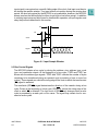
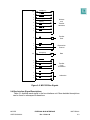
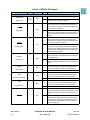
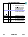
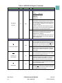
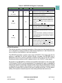
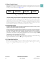
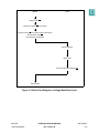
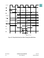
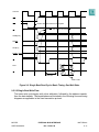
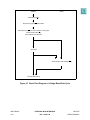
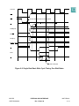
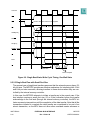
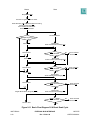
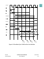
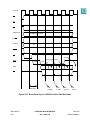
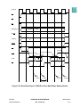
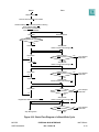
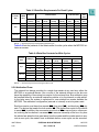
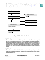
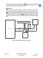
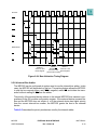
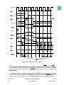
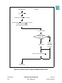
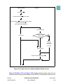
SECTION 9
EXTERNAL BUS INTERFACE
The MPC555 bus is a synchronous, burstable bus. Signals driven on this bus are
required to make the setup and hold time relative to the bus clock’s rising edge. The
bus has the ability to support multiple masters. The MPC555 architecture supports
byte, half-word, and word operands allowing access to 8-, 16-, and 32-bit data ports
through the use of synchronous cycles controlled by the size outputs (TSIZ0, TSIZ1).
For accesses to 16- and 8-bit ports, the slave must be controlled by the memory
controller.
9.1 Features
The external bus interface features are listed below.
• 32-bit address bus with transfer size indication (only 24 available on pins)
• 32-bit data bus
• Bus arbitration logic on-chip supports an external master
• Internal chip-select and wait state generation to support peripheral or static memory devices through the memory controller
• Supports various memory (SRAM, EEPROM) types: synchronous and asynchronous, burstable and non-burstable
• Supports non-wrap bursts
• Flash ROM programming support
• Compatible with PowerPC architecture
• Easy to interface to slave devices
• Bus is synchronous (all signals are referenced to rising edge of bus clock)
• Bus can operate at the same frequency as the MPC555 or half the frequency.
9.2 Bus Transfer Signals
The bus transfers information between the MPC555 and external memory of a peripheral device. External devices can accept or provide 8, 16, and 32 bits in parallel and
must follow the handshake protocol described in this section. The maximum number
of bits accepted or provided during a bus transfer is defined as the port width.
The MPC555 contains an address bus that specifies the address for the transfer and
a data bus that transfers the data. Control signals indicate the beginning and type of
the cycle, as well as the address space and size of the transfer. The selected device
then controls the length of the cycle with the signal(s) used to terminate the cycle. A
strobe signal for the address bus indicates the validity of the address and provides timing information for the data.
The MPC555 bus is synchronous. The bus and control input signals must be timed to
setup and hold times relative to the rising edge of the clock. Bus cycles can be completed in two clock cycles.
For all inputs, the MPC555 latches the level of the input during a sample window
around the rising edge of the clock signal. This window is illustrated in Figure 9-1,
where tsu and tho are the input setup and hold times, respectively. To ensure that an
MPC555
USER’S MANUAL
EXTERNAL BUS INTERFACE
Rev. 15 Nov 98
MOTOROLA
9-1
input signal is recognized on a specific falling edge of the clock, that input must be stable during the sample window. If an input makes a transition during the window time
period, the level recognized by the MPC555 is not predictable; however, the MPC555
always resolves the latched level to either a logic high or low before using it. In addition
to meeting input setup and hold times for deterministic operation, all input signals must
obey the protocols described in this section.
tho
tsu
Clock
Signal
Sample
Window
Figure 9-1 Input Sample Window
9.3 Bus Control Signals
The MPC555 initiates a bus cycle by driving the address, size, address type, cycle
type, and read/write outputs. At the beginning of a bus cycle, TSIZ0 and TSIZ1 are
driven with the address type signals. TSIZ0 and TSIZ1 indicate the number of bytes
remaining to be transferred during an operand cycle (consisting of one or more bus
cycles). These signals are valid at the rising edge of the clock in which the transfer start
(TS) signal is asserted.
The read/write (RD/WR) signal determines the direction of the transfer during a bus
cycle. Driven at the beginning of a bus cycle, RD/WR is valid at the rising edge of the
clock in which TS is asserted. The logic level of RD/WR only changes when a write
cycle is preceded by a read cycle or vice versa. The signal may remain low for consecutive write cycles.
MOTOROLA
9-2
EXTERNAL BUS INTERFACE
Rev. 15 Nov 98
MPC555
USER’S MANUAL
32
1
1
2
4
1
ADDR[0:31]
RD/WR
BURST
TSIZ[0:1]
PTR
1
STS (BI)
1
BDIP
1
TS
1
RSV
1
1
32
1
1
1
1
1
1
1
Address
and
Transfer
Attributes
AT[0:3]
KR
CR
Transfer
Start
Reservation
Protocol
DATA[0:31]
Data
RETRY
BI (STS)
TA
TEA
Transfer
Cycle
Termination
BR
BG
Arbitration
BB
Figure 9-2 MPC555 Bus Signals
9.4 Bus Interface Signal Descriptions
Table 5-1 diatribes each signal in the bus interface unit. More detailed descriptions
can be found in subsequent subsections.
MPC555
USER’S MANUAL
EXTERNAL BUS INTERFACE
Rev. 15 Nov 98
MOTOROLA
9-3
.
Table 9-1 MPC555 SIU Signals
Signal Name
Pins
Active
I/O
Description
Address and Transfer Attributes
ADDR[0:31]
Address bus
24
(8:31)
High
O
Specifies the physical address of the bus transaction.
I
Driven by an external bus master when it owns the external bus. Only for testing purposes.
O
Driven by the MPC555 along with the address when it
owns the external bus. Driven high indicates that a
read access is in progress. Driven low indicates that a
write access is in progress.
I
Driven by an external master when it owns the external bus. Driven high indicates that a read access is in
progress. Driven low indicates that a write access is in
progress.
O
Driven by the MPC555 along with the address when it
owns the external bus. Driven low indicates that a
burst transfer is in progress. Driven high indicates that
the current transfer is not a burst.
I
Driven by an external master when it owns the external bus. Driven low indicates that a burst transfer is in
progress. Driven high indicates that the current transfer is not a burst. The MPC555 does not support burst
accesses to internal slaves.
O
Driven by the MPC555 along with the address when it
owns the external bus. Specifies the data transfer size
for the transaction.
I
Driven by an external master when it owns the external bus. Specifies the data transfer size for the transaction.
O
Driven by the MPC555 along with the address when it
owns the external bus. Indicates additional information about the address on the current transaction.
I
Only for testing purposes.
O
Driven by the MPC555 along with the address when it
owns the external bus. Indicates additional information about the address on the current transaction.
I
Only for testing purposes.
O
Driven by the MPC555 along with the address when it
owns the external bus. Indicates additional information about the address on the current transaction.
I
Only for testing purposes.
I
In the case of regular transaction, this signal is driven
by the slave device to indicate that the MPC555 must
relinquish the ownership of the bus and retry the cycle.
O
When an external master owns the bus and the internal MPC555 bus initiates access to the external bus
at the same time, this signal is used to cause the external master to relinquish the bus for one clock to
solve the contention.
RD/WR
1
HIgh
Read/write
BURST
1
Low
Burst transfer
TSIZ[0:1]
2
High
Transfer size
AT[0:3]
3
High
Address type
RSV
1
Low
Reservation transfer
PTR
1
High
Program trace
RETRY
MOTOROLA
9-4
1
Low
EXTERNAL BUS INTERFACE
Rev. 15 Nov 98
MPC555
USER’S MANUAL
Table 9-1 MPC555 SIU Signals (Continued)
Signal Name
Pins
Active
I/O
Description
O
Driven by the MPC555 when it owns the external bus.
It is part of the burst protocol. When BDIP is asserted,
the second beat in front of the current one is requested by the master. This signal is negated prior to the
end of a burst to terminate the burst data phase early.
I
Driven by an external master when it owns the external bus. When BDIP is asserted, the second beat in
front of the current one is requested by the master.
This signal is negated prior to the end of a burst to terminate the burst data phase early. The MPC555 does
not support burst accesses to internal slaves.
BDIP
1
Low
Burst data in progress
Transfer Start
O
Driven by the MPC555 when it owns the external bus.
Indicates the start of a transaction on the external bus.
I
Driven by an external master when it owns the external bus. It indicates the start of a transaction on the
external bus or (in show cycle mode) signals the beginning of an internal transaction.
O
Driven by the MPC555 when it owns the external bus.
Indicates the start of a transaction on the external bus
or signals the beginning of an internal transaction in
show cycle mode.
TS
1
Low
Transfer start
STS
1
Low
Special transfer start
Reservation Protocol
I
Each PowerPC CPU has its own CR signal. Assertion
of CR instructs the bus master to clear its reservation;
some other master has touched its reserved space.
This is a pulsed signal.
I
In case of a bus cycle initiated by a STWCX instruction issued by the RCPU to a non-local bus on which
the storage reservation has been lost, this signal is
used by the non-local bus interface to backoff the cycle. Refer to 9.5.9 Storage Reservation for details.
CR
1
Low
Cancel reservation
KR
1
Kill reservation
MPC555
USER’S MANUAL
Low
EXTERNAL BUS INTERFACE
Rev. 15 Nov 98
MOTOROLA
9-5
Table 9-1 MPC555 SIU Signals (Continued)
Signal Name
Pins
Active
I/O
Description
Data
The data bus has the following byte lane assignments:
Data Byte
Byte Lane
DATA[0:7]
0
DATA[8:15]
1
DATA[16:23]
2
DATA[24:31]
3
DATA[0:31]
32
High
O
Data bus
Driven by the MPC555 when it owns the external bus
and it initiated a write transaction to a slave device.
For single beat transactions, the byte lanes not selected for the transfer by ADDR[30:31] and TSIZ[0:1] do
not supply valid data.
In addition, the MPC555 drives DATA[0:31] when an
external master owns the external bus and initiated a
read transaction to an internal slave module.
I
Driven by the slave in a read transaction. For single
beat transactions, the MPC555 does not sample byte
lanes that are not selected for the transfer by
ADDR[30:31] and TSIZ[0:1].
In addition, an external master that owns the bus and
initiated a write transaction to an internal slave module drives DATA[0:31].
Transfer Cycle Termination
I
Driven by the slave device to which the current transaction was addressed. Indicates that the slave has received the data on the write cycle or returned data on
the read cycle. If the transaction is a burst, TA should
be asserted for each one of the transaction beats.
O
Driven by the MPC555 when the slave device is controlled by the on-chip memory controller or when an
external master initiated a transaction to an internal
slave module.
I
Driven by the slave device to which the current transaction was addressed. Indicates that an error condition has occurred during the bus cycle.
O
Driven by the MPC555 when the internal bus monitor
detected an erroneous bus condition, or when an external master initiated a transaction to an internal
slave module and an internal error was detected.
I
Driven by the slave device to which the current transaction was addressed. Indicates that the current slave
does not support burst mode.
O
Driven by the MPC555 when the slave device is controlled by the on-chip memory controller. the MPC555
also asserts BI for any external master burst access
to internal MPC555 memory space.
TA
1
LOW
Transfer acknowledge
TEA
Transfer error
acknowledge
1
Low
BI
1
Burst inhibit
MOTOROLA
9-6
Low
EXTERNAL BUS INTERFACE
Rev. 15 Nov 98
MPC555
USER’S MANUAL
Table 9-1 MPC555 SIU Signals (Continued)
Signal Name
Pins
Active
I/O
Description
ARBITRATION
BR
1
I
When the internal arbiter is enabled, BR assertion indicates that an external master is requesting the bus.
O
Driven by the MPC555 when the internal arbiter is disabled and the chip is not parked.
Low
Bus request
O
BG
1
Low
Bus grant
When the internal arbiter is enabled, the MPC555 asserts this signal to indicate that an external master
may assume ownership of the bus and begin a bus
transaction. The BG signal should be qualified by the
master requesting the bus in order to ensure it is the
bus owner:
Qualified bus grant = BG & ~ BB
I
When the internal arbiter is disabled, BG is sampled
and properly qualified by the MPC555 when an external bus transaction is to be executed by the chip.
When the internal arbiter is enabled, the MPC555 asserts this signal to indicate that it is the current owner
of the bus.
O
BB
1
Low
Bus busy
I
When the internal arbiter is disabled, the MPC555 asserts this signal after the external arbiter has granted
the ownership of the bus to the chip and it is ready to
start the transaction.
When the internal arbiter is enabled, the MPC555
samples this signal to get indication of when the external master ended its bus tenure (BB negated).
When the internal arbiter is disabled, the BB is sampled to properly qualify the BG line when an external
bus transaction is to be executed by the chip.
9.5 Bus Operations
This section provides a functional description of the system bus, the signals that control it, and the bus cycles provided for data transfer operations. It also describes the
error conditions, bus arbitration, and reset operation.
The MPC555 generates a system clock output (CLKOUT). This output sets the frequency of operation for the bus interface directly. Internally, the MPC555 uses a
phase-lock loop (PLL) circuit to generate a master clock for all of the CPU circuitry
(including the bus interface) which is phase-locked to the CLKOUT output signal.
All signals for the MPC555 bus interface are specified with respect to the rising edge
of the external CLKOUT and are guaranteed to be sampled as inputs or changed as
outputs with respect to that edge. Since the same clock edge is referenced for driving
or sampling the bus signals, the possibility of clock skew could exist between various
modules in a system due to routing or the use of multiple clock lines. It is the responsibility of the system to handle any such clock skew problems that could occur.
MPC555
USER’S MANUAL
EXTERNAL BUS INTERFACE
Rev. 15 Nov 98
MOTOROLA
9-7
9.5.1 Basic Transfer Protocol
The basic transfer protocol defines the sequence of actions that must occur on the
MPC555 bus to perform a complete bus transaction. A simplified scheme of the basic
transfer protocol is illustrated in Figure 9-3.
Arbitration
Address Transfer
Data Transfer
Termination
Figure 9-3 Basic Transfer Protocol
The basic transfer protocol provides for an arbitration phase and an address and data
transfer phase. The address phase specifies the address for the transaction and the
transfer attributes that describe the transaction. The data phase performs the transfer
of data (if any is to be transferred). The data phase may transfer a single beat of data
(4 bytes or less) for nonburst operations, a 4-beat burst of data (4 x 4 bytes), an 8-beat
burst of data (8 x 2 bytes) or a 16-beat burst of data (16 x 1 bytes).
9.5.2 Single Beat Transfer
During the data transfer phase, the data is transferred from master to slave (in write
cycles) or from slave to master (on read cycles).
During a write cycle, the master drives the data as soon as it can, but never earlier than
the cycle following the address transfer phase. The master has to take into consideration the “one dead clock cycle” switching between drivers to avoid electrical
contentions. The master can stop driving the data bus as soon as it samples the TA
line asserted on the rising edge of the CLKOUT.
During a read cycle, the master accepts the data bus contents as valid at the rising
edge of the CLKOUT in which the TA signal is sampled/asserted.
9.5.2.1 Single Beat Read Flow
The basic read cycle begins with a bus arbitration, followed by the address transfer,
then the data transfer. The handshakes are illustrated in the following flow and timing
diagrams as applicable to the fixed transaction protocol.
MOTOROLA
9-8
EXTERNAL BUS INTERFACE
Rev. 15 Nov 98
MPC555
USER’S MANUAL
Master
Slave
Request bus (BR)
Receive bus grant (BG) from arbiter
Assert bus busy (BB) if no other master is driving bus
Assert transfer start (TS)
Drive address and attributes
Receive address
Return data
Assert transfer acknowledge (TA)
Receive data
Figure 9-4 Basic Flow Diagram of a Single Beat Read Cycle
MPC555
USER’S MANUAL
EXTERNAL BUS INTERFACE
Rev. 15 Nov 98
MOTOROLA
9-9
CLKOUT
BR
BG
Receive bus grant and bus busy negated
O
O
Assert BB, drive address and assert TS
BB
O
ADDR[0:31]
RD/WR
TSIZ[0:1]
BURST, BDIP
TS
O
Data
TA
O
Data is valid
Figure 9-5 Single Beat Read Cycle–Basic Timing–Zero Wait States
MOTOROLA
9-10
EXTERNAL BUS INTERFACE
Rev. 15 Nov 98
MPC555
USER’S MANUAL
CLKOUT
BR
BG
Receive bus grant and bus busy negated
O
O
assert BB, drive address and assert TS
BB
O
ADDR[0:31]
RD/WR
TSIZ[0:1]
BURST, BDIP
TS
O
Data
TA
Wait state
O
Data is valid
Figure 9-6 Single Beat Read Cycle–Basic Timing–One Wait State
9.5.2.2 Single Beat Write Flow
The basic write cycle begins with a bus arbitration, followed by the address transfer,
then the data transfer. The handshakes are illustrated in the following flow and timing
diagrams as applicable to the fixed transaction protocol.
MPC555
USER’S MANUAL
EXTERNAL BUS INTERFACE
Rev. 15 Nov 98
MOTOROLA
9-11
Master
Slave
Request bus (BR)
Receive bus grant (BG) from arbiter
Assert bus busy (BB) if no other master is driving bus
Assert transfer start (TS)
Drive address and attributes
Drive data
Assert transfer acknowledge (TA)
Interrupt data driving
Figure 9-7 Basic Flow Diagram of a Single Beat Write Cycle
MOTOROLA
9-12
EXTERNAL BUS INTERFACE
Rev. 15 Nov 98
MPC555
USER’S MANUAL
CLKOUT
BR
BG
Receive bus grant and bus busy negated
O
O
Assert BB, drive address and assert TS
BB
O
ADDR[0:31]
RD/WR
TSIZ[0:1]
BURST, BDIP
TS
O
Data
TA
O
Data is sampled
Figure 9-8 Single Beat Basic Write Cycle Timing, Zero Wait States
MPC555
USER’S MANUAL
EXTERNAL BUS INTERFACE
Rev. 15 Nov 98
MOTOROLA
9-13
CLKOUT
BR
Receive bus grant and bus busy negated
BG
O
O
Assert BB, drive address and assert TS
BB
O
ADDR[0:31]
RD/WR
TSIZ[0:1]
BURST, BDIP
TS
O
Data
TA
Wait state
O
Data is sampled
Figure 9-9 Single Beat Basic Write Cycle Timing, One Wait State
9.5.2.3 Single Beat Flow with Small Port Size
The general case of single beat transfers assumes that the external memory has a 32bit port size. The MPC555 provides an effective mechanism for interfacing with 16-bit
and 8-bit port size memories, allowing transfers to these devices when they are controlled by the internal memory controller.
In this case, the MPC555 attempts to initiate a transfer as in the normal case. If the
bus interface receives a small port size (16 or 8 bits) indication before the transfer
acknowledge to the first beat (through the internal memory controller), the MCU initiates successive transactions until the completion of the data transfer. Note that all the
transactions initiated to complete the data transfer are considered to be part of an
atomic transaction, so the MCU does not allow other unrelated master accesses or
MOTOROLA
9-14
EXTERNAL BUS INTERFACE
Rev. 15 Nov 98
MPC555
USER’S MANUAL
bus arbitration to intervene between the transfers. If any of the transactions except the
first is re-tried during an access to a small port, then an exception is generated to the
RCPU.
CLKOUT
BR
BG
BB
ADDR[0:1]
ADDR + 2
ADDR
RD/WR
TSIZ[0:1]
10
00
BURST, BDIP
TS
STS
Data
ABCDEFGH
EFGHEFGH
TA
Figure 9-10 Single Beat 32-Bit Data
Write Cycle Timing, 16 Bit-Port Size
9.5.3 Burst Transfer
The MPC555 uses non-wrapping burst transfers to access operands of up to 16 bytes
(four words). A non-wrapping burst access stops accessing the external device when
the word address is modulo four. The MPC555 begins the access by supplying a starting address that points to one of the words and requiring the memory device to
sequentially drive or sample each word on the data bus. The selected slave device
MPC555
USER’S MANUAL
EXTERNAL BUS INTERFACE
Rev. 15 Nov 98
MOTOROLA
9-15
must internally increment ADDR28 and ADDR29 (and ADDR30 in the case of a 16-bit
port slave device, and also ADDR31 in the case of an 8-bit port slave device) of the
supplied address for each transfer, causing the address to reach a four-word boundary, and then stop. The address and transfer attributes supplied by the MPC555
remain stable during the transfers. The selected device terminates each transfer by
driving or sampling the word on the data bus and asserting TA.
The MPC555 also supports burst-inhibited transfers for slave devices that are unable
to support bursting. For this type of bus cycle, the selected slave device supplies or
samples the first word the MPC555 points to and asserts the burst-inhibit signal with
TA for the first transfer of the burst access. The MPC555 responds by terminating the
burst and accessing the remainder of the 16-byte block. These remaining accesses
use up to three read/write bus cycles (each one for a word) in the case of a 32-bit port
width slave, up to seven read/write bus cycles in the case of a 16-bit port width slave,
or up to fifteen read/write bus cycles in the case of a 8-bit port width slave.
The general case of burst transfers assumes that the external memory has a 32-bit
port size. The MPC555 provides an effective mechanism for interfacing with 16-bit port
size memories and 8-bit port size memories allowing bursts transfers to these devices
when they are controlled by the internal memory controller.
In this case, the MPC555 attempts to initiate a burst transfer as in the normal case. If
the memory controller signals to the bus interface that the external device has a small
port size (8 or 16 bits), and if the burst is accepted, the bus interface completes a burst
of 8 or 16 beats.
Each of the data beats of the burst transfers effectively only one or two bytes. Note
that this burst of 8 or 16 beats is considered an atomic transaction, so the MPC555
does not allow other unrelated master accesses or bus arbitration to intervene
between the transfers.
9.5.4 Burst Mechanism
In addition to the standard bus signals, the MPC555 burst mechanism uses the following signals:
• The BURST signal indicates that the cycle is a burst cycle.
• The burst data in progress (BDIP) signal indicates the duration of the burst data.
• The burst inhibit (BI) signal indicates whether the slave is burstable.
At the start of the burst transfer, the master drives the address, the address attributes,
and the BURST signal to indicate that a burst transfer is being initiated, and asserts
TS. If the slave is burstable, it negates the burst-inhibit (BI) signal. If the slave cannot
burst, it asserts BI.
During the data phase of a burst write cycle the master drives the data. It also asserts
BDIP if it intends to drive the data beat following the current data beat. When the slave
has received the data, it asserts the signal transfer acknowledge to indicate to the
master that it is ready for the next data transfer. The master again drives the next data
and asserts or negates the BDIP signal. If the master does not intend to drive another
MOTOROLA
9-16
EXTERNAL BUS INTERFACE
Rev. 15 Nov 98
MPC555
USER’S MANUAL
data beat following the current one, it negates BDIP to indicate to the slave that the
next data beat transfer is the last data of the burst write transfer.
BDIP has two basic timings: normal and late (see Figure 9-13 and Figure 9-14). In the
late timing mode, assertion of BDIP is delayed by the number of wait states in the first
data beat. This implies that for zero-wait-state cycles, BDIP assertion time is identical
in normal and late modes. Cycles with late BDIP generation can occur only during
cycles for which the memory controller generates TA internally. Refer to SECTION 10
MEMORY CONTROLLER for more information.
In the MPC555, no internal master initiates write bursts. The MPC555 is designed to
perform this kind of transaction in order to support an external master that is using the
memory controller services. Refer to 10.7 Memory Controller External Master
Support.
During the data phase of a burst read cycle, the master receives data from the
addressed slave. If the master needs more than one data beat, it asserts BDIP. Upon
receiving the second-to-last data beat, the master negates BDIP. The slave stops driving new data after it receives the negation of the BDIP signal at the rising edge of the
clock.
MPC555
USER’S MANUAL
EXTERNAL BUS INTERFACE
Rev. 15 Nov 98
MOTOROLA
9-17
Master
Slave
Request Bus (BR)
Receive bus grant (BG) from arbiter
Assert Bus Busy (BB) if No Other Master is Driving
Assert Transfer Start (TS)
Drive Address and Attributes
Drive BURST Asserted
Receive Address
ADDR[28:29] mod 4 = ?
=0
Assert BDIP
Return Data
Assert Transfer Acknowledge (TA)
Receive Data
BDIP Asserted
=1
No
Drive Last Data
& Assert TA
Yes
Return Data
Assert Transfer Acknowledge (TA)
Assert BDIP
Receive Data
BDIP Asserted
=2
Drive Last Data
& Assert TA
No
Yes
Assert BDIP
Return Data
Assert Transfer Acknowledge (TA)
Receive Data
BDIP Asserted
No
Drive Last Data
& Assert TA
=3
Yes
Negate Burst Data in Progress (BDIP)
Return Data
Assert Transfer Acknowledge (TA)
BDIP Asserted
Receive Sata
No
Drive Last Data
& Assert TA
Yes
Figure 9-11 Basic Flow Diagram Of A Burst Read Cycle
MOTOROLA
9-18
EXTERNAL BUS INTERFACE
Rev. 15 Nov 98
MPC555
USER’S MANUAL
CLKOUT
BR
BG
BB
ADDR[0:31]
ADDR[28:31] = 0000
RD/WR
TSIZ[0:1]
00
BURST
TS
Last Beat
O
Expects Another Data
BDIP
O
O
O
Data
TA
O
O
Data
is Valid
O
Data
is Valid
O
Data
is Valid
Data
is Valid
Figure 9-12 Burst-Read Cycle–32-Bit Port Size–Zero Wait State
MPC555
USER’S MANUAL
EXTERNAL BUS INTERFACE
Rev. 15 Nov 98
MOTOROLA
9-19
CLKOUT
BR
BG
BB
ADDR[0:31]
ADDR[28:31] = 0000
RD/WR
TSIZ[0:1]
00
BURST
TS
Last Beat
O
Expects Another Data
BDIP
Normal
Late
O
O
O
Data
TA
O
Wait State
O
Data
is Valid
O
Data
is Valid
O
Data
is Valid
Data
is Valid
Figure 9-13 Burst-Read Cycle–32-Bit Port Size–One Wait State
MOTOROLA
9-20
EXTERNAL BUS INTERFACE
Rev. 15 Nov 98
MPC555
USER’S MANUAL
CLKOUT
BR
BG
BB
ADDR[0:31]
ADDR[28:31] = 0000
RD/WR
TSIZ[0:1]
00
BURST
TS
Last Beat
BDIP
Normal or Late
O
Expects Another Data
O
O
O
O
O
Data
TA
Data
is Valid
O
Data
is Valid
O
Data
is Valid
Data
is Valid
Wait State
Figure 9-14 Burst-Read Cycle–32-Bit Port Size–Wait States Between Beats
MPC555
USER’S MANUAL
EXTERNAL BUS INTERFACE
Rev. 15 Nov 98
MOTOROLA
9-21
CLKOUT
BR
BG
BB
ADDR[0:31]
ADDR[28:31] = 0000
RD/WR
TSIZ[0:1]
00
BURST
TS
BDIP
Data[0:15]
TA
Figure 9-15 Burst-Read Cycle, 16-Bit Port Size
MOTOROLA
9-22
EXTERNAL BUS INTERFACE
Rev. 15 Nov 98
MPC555
USER’S MANUAL
Master
Slave
Request Bus (BR)
Receive Bus Grant (BG) from Arbiter
Assert Bus Busy (BB) if No Other Master is Driving
Assert Transfer Start (TS)
Drive Address and Attributes
Drive BURST Asserted
Drive data
Receive Address
ADDR[28:29] mod 4 = ?
=0
Assert BDIP
Sample Data
Assert Transfer Acknowledge (TA)
Drive Data
BDIP Asserted
=1
No
Don’t Sample
Next Data
Yes
Sample Data
Assert Transfer Acknowledge (TA)
Assert BDIP
Drive Data
BDIP Asserted
=2
No
Don’t Sample
Next Data
No
Don’t Sample
Next Data
Yes
Assert BDIP
Sample Data
Assert Transfer Acknowledge (TA)
Drive Data
BDIP Asserted
=3
Yes
Negate Burst Data in Progress (BDIP)
Sample Data
Assert Transfer Acknowledge (TA)
BDIP Asserted
Stop Driving Data
No
Don’t Sample
Next Data
Yes
Figure 9-16 Basic Flow Diagram of a Burst Write Cycle
MPC555
USER’S MANUAL
EXTERNAL BUS INTERFACE
Rev. 15 Nov 98
MOTOROLA
9-23
CLKOUT
BR
BG
BB
ADDR[0:31]
ADDR[28:29] = 00
RD/WR
TSIZ[0:1]
00
BURST
TS
Last Beat
O
Will Drive Another Data
BDIP
O
O
O
O
O
O
Data
TA
O
Data
Data
Data
is Sampled is Sampled is Sampled
Data
is Sampled
Figure 9-17 Burst-Write Cycle, 32-Bit Port Size, Zero Wait States
MOTOROLA
9-24
EXTERNAL BUS INTERFACE
Rev. 15 Nov 98
MPC555
USER’S MANUAL
CLKOUT
BR
BG
BB
ADDR[0:27]
ADDR[28:29]
0
1
2
3
ADDR[30:31]
RD/WR
TSIZ[0:1]
00
BURST*
TS
BDIP*
Data
TA
BI
* BURST and BDIP will be asserted for one cycle if the RCPU core requests a burst,
but the USIU splits it into a sequence of normal cycles.
Figure 9-18 Burst-Inhibit Cycle, 32-Bit Port Size (Emulated Burst)
MPC555
USER’S MANUAL
EXTERNAL BUS INTERFACE
Rev. 15 Nov 98
MOTOROLA
9-25
CLKOUT
BR
BG
BB
ADDR(0:29)
n (n modulo 4 = 1)
ADDR[30:31]
RD/WR
TSIZ[0:1]
00
BURST
TS
Expects Another Data
BDIP
O
O
Data
TA
BI
Figure 9-19 Non-Wrap Burst with Three Beats
MOTOROLA
9-26
EXTERNAL BUS INTERFACE
Rev. 15 Nov 98
MPC555
USER’S MANUAL
CLKOUT
BR
BG
BB
ADDR[0:29]
ADDR[30:31]
n (n modulo 4 = 3)
00
RD/WR
TSIZ[0:1]
00
BURST
TS
Is Never Asserted
BDIP
First and Last Beat
Data
TA
O
DATA
is Sampled
Figure 9—2. Non-Wrap Burst with One Data Beat
MPC555
USER’S MANUAL
EXTERNAL BUS INTERFACE
Rev. 15 Nov 98
MOTOROLA
9-27
9.5.5 Alignment and Packaging of Transfers
The MPC555 external bus requires natural address alignment:
• Byte accesses allow any address alignment
• Half-word accesses require address bit 31 to equal zero
• Word accesses require address bits 30 – 31 to equal zero
• Burst accesses require address bits 30 – 31 to equal zero
The MPC555 performs operand transfers through its 32-bit data port. If the transfer is
controlled by the internal memory controller, the MPC555 can support 8- and 16-bit
data port sizes.
The bus requires that the portion of the data bus used for a transfer to or from a particular port size be fixed. A 32-bit port must reside on DATA[0:31], a 16-bit port must
reside on DATA[0:15], and an 8-bit port must reside on DATA[0:7]. The MPC555
always tries to transfer the maximum amount of data on all bus cycles. For a word
operation, it always assumes that the port is 32 bits wide when beginning the bus
cycle.
In Figure 9-20, Figure 9-21, Table 9-3, and Table 9-4, the following conventions are
used:
• OP0 is the most-significant byte of a word operand and OP3 is the least-significant byte.
• The two bytes of a half-word operand are either OP0 (most-significant) and OP1
or OP2 (most-significant) and OP3, depending on the address of the access.
• The single byte of a byte-length operand is OP0, OP1, OP2, or OP3, depending
on the address of the access.
0
31
OP0
OP1
OP0
OP1
OP2
OP3
OP2
OP3
Word
Half-word
OP0
OP1
Byte
OP2
OP3
Figure 9-20 Internal Operand Representation
Figure 9-21 illustrates the device connections on the data bus.
MOTOROLA
9-28
EXTERNAL BUS INTERFACE
Rev. 15 Nov 98
MPC555
USER’S MANUAL
0
31
OP0
OP1
DATA[0:7]
OP2
DATA[8:15]
OP0
OP1
OP0
OP1
OP2
OP3
Interface
Output
Register
OP3
DATA[16:23]
OP2
DATA[24:31]
OP3
32-bit Port Size
16-bit Port Size
OP0
OP1
8-bit Port Size
OP2
OP3
Figure 9-21 Interface To Different Port Size Devices
Table 9-3 lists the bytes required on the data bus for read cycles.
MPC555
USER’S MANUAL
EXTERNAL BUS INTERFACE
Rev. 15 Nov 98
MOTOROLA
9-29
Table 9-3 Data Bus Requirements For Read Cycles
Transfer
Size
TSIZE
[0:1]
Byte
Half-word
Word
Address
32-bit Port Size
16-bit Port Size
8-bit
Port
Size
ADDR
[30:31]
DATA
[0:7]
DATA
[8:15]
DATA
[16:23]
DATA
[24:31]
DATA
[0:7]
DATA
[8:15]
DATA
[0:7]
01
00
OP0
—
—
—
OP0
—
OP0
01
01
—
OP1
—
—
—
OP1
OP1
01
10
—
—
OP2
—
OP2
—
OP2
01
11
—
—
—
OP3
—
OP3
OP3
10
00
OP0
OP1
—
—
OP0
OP1
OP0
10
10
—
—
OP2
OP3
OP2
OP3
OP2
00
00
OP0
OP1
OP2
OP3
OP0
OP1
OP0
NOTE: “—” denotes a byte not required during that read cycle.
Table 9-4 lists the patterns of the data transfer for write cycles when the MPC555 initiates an access.
Table 9-4 Data Bus Contents for Write Cycles
Transfer
Size
Byte
Half-word
Word
Address
External Data Bus Pattern
TSIZE[0:1]
ADDR
[30:31]
DATA
[0:7]
DATA
[8:15]
DATA
[16:23]
DATA
[24:31]
01
00
OP0
—
—
—
01
01
OP1
OP1
—
—
01
10
OP2
—
OP2
—
01
11
OP3
OP3
—
OP3
10
00
OP0
OP1
—
—
10
10
OP2
OP3
OP2
OP3
00
00
OP0
OP1
OP2
OP3
NOTE: “—” denotes a byte not driven during that write cycle.
9.5.6 Arbitration Phase
The external bus design provides for a single bus master at any one time, either the
MPC555 or an external device. One or more of the external devices on the bus can
have the capability of becoming bus master for the external bus. Bus arbitration may
be handled either by an external central bus arbiter or by the internal on-chip arbiter.
In the latter case, the system is optimized for one external bus master besides the
MPC555. The arbitration configuration (external or internal) is set at system reset.
Each bus master must have bus request (BR), bus grant (BG), and bus busy (BB) signals. The device that needs the bus asserts BR. The device then waits for the arbiter
to assert BG. In addition, the new master must look at BB to ensure that no other master is driving the bus before it can assert BB to assume ownership of the bus. Any time
the arbiter has taken the bus grant away from the master and the master wants to execute a new cycle, the master must re-arbitrate before a new cycle can be executed.
MOTOROLA
9-30
EXTERNAL BUS INTERFACE
Rev. 15 Nov 98
MPC555
USER’S MANUAL
The MPC555, however, guarantees data coherency for access to a small port size and
for decomposed bursts. This means that the MPC555 will not release the bus before
the completion of the transactions that are considered atomic. Figure 9-22 describes
the basic protocol for bus arbitration.
Requesting Device
Arbiter
Request the Bus
1. Assert BR
GRANT Bus arbitration
1.Assert BG
Acknowledge Bus Mastership
1. Wait for BB to be negated.
2. Assert BB to becom enext master
Terminate Arbitration
3. Negate BR
1. Negate BG (or keep asserted to park
bus master
Operate as bus Master
1. Perform data transfer
Release Bus Mastership
1. Negate BB
Figure 9-22 Bus Arbitration Flowchart
9.5.6.1 Bus Request
The potential bus master asserts BR to request bus mastership. BR should be negated
as soon as the bus is granted, the bus is not busy, and the new master can drive the
bus. If more requests are pending, the master can keep asserting its bus request as
long as needed. When configured for external central arbitration, the MPC555 drives
this signal when it requires bus mastership. When the internal on-chip arbiter is used,
this signal is an input to the internal arbiter and should be driven by the external bus
master.
9.5.6.2 Bus Grant
The arbiter asserts BG to indicate that the bus is granted to the requesting device. This
signal can be negated following the negation of BR or kept asserted for the current
master to park the bus.
MPC555
USER’S MANUAL
EXTERNAL BUS INTERFACE
Rev. 15 Nov 98
MOTOROLA
9-31
When configured for external central arbitration, BG is an input signal to the MPC555
from the external arbiter. When the internal on-chip arbiter is used, this signal is an output from the internal arbiter to the external bus master.
9.5.6.3 Bus Busy
BB assertion indicates that the current bus master is using the bus. New masters
should not begin transfer until this signal is negated. The bus owner should not relinquish or negate this signal until the transfer is complete. To avoid contention on the
BB line, the master should three-state this signal when it gets a logical one value. This
requires the connection of an external pull-up resistor to ensure that a master that
acquires the bus is able to recognize the BB line negated, regardless of how many
cycles have passed since the previous master relinquished the bus. Refer to Figure
9-23.
Master
External Bus
TS
MPC555
BB
Slave 2
Figure 9-23 Masters Signals Basic Connection
MOTOROLA
9-32
EXTERNAL BUS INTERFACE
Rev. 15 Nov 98
MPC555
USER’S MANUAL
CLKOUT
BR0
BG0
BR1
BG1
BB
ADDR & Attr.
TS
TA
Master 0
“Turns On” and
Drives Signals
Master 0
Master 1
Negates BB
“Turns On” and
and “Turns Off” Drives Signals
(Three-state Controls)
Figure 9-24 Bus Arbitration Timing Diagram
9.5.6.4 Internal Bus Arbiter
The MPC555 can be configured at system reset to use the internal bus arbiter. In this
case, the MPC555 will be parked on the bus. The parking feature allows the MPC555
to skip the bus request phase, and if BB is negated, assert BB and initiate the transaction without waiting for BG from the arbiter.
The priority of the external device relative to the internal MPC555 bus masters is programmed in the SIU module configuration register. If the external device requests the
bus and the MPC555 does not require it, or if the external device has higher priority
than the current internal bus master, the MPC555 grants the bus to the external
device.
Table 9-5 describes the priority mechanism used by the internal arbiter.
MPC555
USER’S MANUAL
EXTERNAL BUS INTERFACE
Rev. 15 Nov 98
MOTOROLA
9-33
Table 9-5 Priority Between Internal and External Masters over External Bus1
Type
Direction
Priority
Parked access2
Internal → external
0
Instruction access
Internal → external
3
Data access
Internal → external
4
External access
external → external/internal
EARP3 (could be programmed to 0 – 7)
NOTES:
1. External master will be granted external bus ownership if EARP is greater than the internal access priority.
2. Parked access is instruction or data access from the RCPU which is initiated on the internal bus without
requesting it first in order to improve performance.
3. Refer to 6.13.1.1 SIU Module Configuration Register.
Figure 9-25 illustrates the internal finite-state machine that implements the arbiter
protocol.
MOTOROLA
9-34
EXTERNAL BUS INTERFACE
Rev. 15 Nov 98
MPC555
USER’S MANUAL
External
Owner
BG = 0
BB = t.s
MPC555 Internal Master With Higher
Priority than the External Device
Requires the Bus
1,
B
R
=1
BR
=
0
External Master
Requests Bus
BB
=
BR = 1
Ext Master
Release Bus
BB = 0
IDLE
MPC555 Bus
Wait
BG = 1
BB = t.s
BG = 1
BB = t.s
MCU Needs
the Bus
BB = 1
MPC555 No Longer
Needs the Bus
MPC555
Owner
BR = 0
BG = 1
BB = 0
External Device With Higher
Priority than the Current Internal
Bus Master Requests the Bus
MPC555 Still Needs
the Bus
Figure 9-25 Internal Bus Arbitration State Machine
9.5.7 Address Transfer Phase Signals
Address transfer phase signals include the following:
• Transfer start
• Address bus
• Transfer attributes
Transfer attributes signals include RD/WR, BURST, TSIZ[0:1], AT[0:3], STS, and
BDIP. With the exception of the BDIP, these signals are available at the same time as
the address bus.
MPC555
USER’S MANUAL
EXTERNAL BUS INTERFACE
Rev. 15 Nov 98
MOTOROLA
9-35
9.5.7.1 Transfer Start
This signal (TS) indicates the beginning of a transaction on the bus addressing a slave
device. This signal should be asserted by a master only after the ownership of the bus
was granted by the arbitration protocol. This signal is asserted for the first cycle of the
transaction only and is negated in successive clock cycles until the end of the transaction. The master should three-state this signal when it relinquishes the bus to avoid
contention between two or more masters in this line. This situation indicates that an
external pull-up resistor should be connected to the TS signal to avoid having a slave
recognize this signal as asserted when no master drives it. Refer to Figure 9-23.
9.5.7.2 Address Bus
The address bus consists of 32 bits, with ADDR0 the most significant bit and ADDR31
the least significant bit. The bus is byte-addressable, so each address can address
one or more bytes. The address and its attributes are driven on the bus with the transfer start signal and kept valid until the bus master receives the transfer acknowledge
signal from the slave. To distinguish the individual byte, the slave device must observe
the TSIZ signals.
9.5.7.3 Read/Write
A high value on the RD/WR line indicates a read access. A low value indicates a write
access.
9.5.7.4 Burst Indicator
BURST is driven by the bus master at the beginning of the bus cycle along with the
address to indicate that the transfer is a burst transfer.
The MPC555 supports a non-wrapping, four-beat maximum, critical word first burst
type. The maximum burst size is 16 bytes. For a 32-bit port, the burst includes four
beats. For a 16-bit port, the burst includes 8 beats. For an 8-bit port, the burst includes
16 beats at most. Note that 8- and 16-bit ports must be controlled by the memory
controller.
The actual size of the burst is determined by the address of the starting word of the
burst. Refer to Table 9-6 and Table 9-7.
Table 9-6 Burst Length and Order
Starting
Address
ADDR[28:29]
Burst Order (Assuming
32-bit Port Size)
Burst Length in
Words (Beats)
Burst Length
in Bytes
00
word 0 → word 1 →
word 2 → word 3
4
16
01
word 1 → word 2 → word 3
3
12
10
word 2 → word 3
2
8
11
word 3
1
4
MOTOROLA
9-36
EXTERNAL BUS INTERFACE
Rev. 15 Nov 98
Comments
BDIP never asserted
MPC555
USER’S MANUAL
9.5.7.5 Transfer Size
The transfer size signals (TSIZ[0:1]) indicate the size of the requested data transfer.
During each transfer, the TSIZ signals indicate how many bytes are remaining to be
transferred by the transaction. The TSIZ signals can be used with BURST and
ADDR[30:31] to determine which byte lanes of the data bus are involved in the transfer. For nonburst transfers, the TSIZ signals specify the number of bytes starting from
the byte location addressed by ADDR[30:31]. In burst transfers, the value of TSIZ is
always 00.
Table 9-7 BURST/TSIZE Encoding
BURST
TSIZ(0:1)
Transfer Size
Negated
01
Byte
Negated
10
Half-word
Negated
11
x
Negated
00
Word
Asserted
00
Burst (16 bytes)
9.5.7.6 Address Types
The address type (AT[0:3]), program trace (PTR), and reservation transfer (RSV) signals are outputs that indicate one of 16 address types. These types are designated as
either a normal or alternate master cycle, user or supervisor, and instruction or data
type. The address type signals are valid at the rising edge of the clock in which the
special transfer start (STS) signal is asserted.
A special use of the PTR and RSV signals is for the reservation protocol described in
9.5.9 Storage Reservation. Refer to 9.5.13 Show Cycle Transactions for information on show cycles.
Table 9-8 summarizes the pins used to define the address type. Table 9-9 lists all the
definitions achieved by combining these pins.
Table 9-8 Address Type Pins
Pin
MPC555
USER’S MANUAL
Function
STS
0 = Special transfer
1 = Normal transfer
TS
0 = Start of transfer
1 = No transfer
AT0
Must equal zero on MPC555
AT1
0 = Supervisor mode
1 = User mode
AT2
0 = Instruction
1 = Data
AT3
Reservation/Program Trace
PTR
0 = Program trace
1 = No program trace
RSV
0 = Reservation data
1 = No reservation
EXTERNAL BUS INTERFACE
Rev. 15 Nov 98
MOTOROLA
9-37
:
Table 9-9 Address Types Definition
STS
TS
AT0
AT1
AT2
AT3
PTR
RSV
1
x
x
x
x
x
1
1
No transfer
0
0
1
RCPU, normal instruction, program trace, supervisor mode
1
1
1
RCPU, normal instruction, supervisor mode
0
1
0
RCPU, reservation data, supervisor mode
1
1
1
RCPU, normal data, supervisor mode
0
0
1
RCPU, normal instruction, program trace, user mode
1
1
1
RCPU, normal instruction, user mode
0
1
0
RCPU, reservation data, user mode
1
1
1
RCPU, normal data, user mode
?
1
1
Reserved
0
0
1
RCPU, show cycle address instruction, program trace, supervisor mode
1
1
1
RCPU, show cycle address instruction, supervisor mode
0
1
0
RCPU, reservation show cycle data, supervisor mode
1
1
1
RCPU, show cycle data, supervisor mode
0
0
1
RCPU, show cycle address instruction, program trace, user
mode
1
1
1
RCPU, show cycle address instruction, user mode
0
1
0
RCPU, reservation show cycle data, user mode
1
1
1
RCPU, show cycle data, user mode
?
1
1
Reserved
0
0
1
01
0
0
1
1
1
?
?
0
0
0
1
1
0
0
1
1
1
?
?
Address Space Definitions
NOTES:
1. Cases in which both TS and STS are asserted indicate normal cycles with the show cycle attribute.
9.5.7.7 Burst Data in Progress
This signal is sent from the master to the slave to indicate that there is a data beat following the current data beat. The master uses this signal to give the slave advance
warning of the remaining data in the burst. BDIP can also be used to terminate the
burst cycle early. Refer to 9.5.3 Burst Transfer and 9.5.4 Burst Mechanism for more
information.
9.5.8 Termination Signals
The EBI uses three termination signals:
• Transfer acknowledge (TA)
• Burst inhibit (BI)
• Transfer error acknowledge (TEA)
9.5.8.1 Transfer Acknowledge
Transfer acknowledge indicates normal completion of the bus transfer. During a burst
cycle, the slave asserts this signal with every data beat returned or accepted.
MOTOROLA
9-38
EXTERNAL BUS INTERFACE
Rev. 15 Nov 98
MPC555
USER’S MANUAL
9.5.8.2 Burst Inhibit
A slave sends the BI signal to the master to indicate that the addressed device does
not have burst capability. If this signal is asserted, the master must transfer in multiple
cycles and increment the address for the slave to complete the burst transfer. For a
system that does not use the burst mode at all, this signal can be tied low permanently.
9.5.8.3 Transfer Error Acknowledge
The TEA signal terminates a bus cycle under one or more bus error conditions. The
current bus cycle must be aborted. This signal overrides any other cycle termination
signals, such as transfer acknowledge.
9.5.8.4 Termination Signals Protocol
The transfer protocol was defined to avoid electrical contention on lines that can be
driven by various sources. To this end, a slave must not drive signals associated with
the data transfer until the address phase is completed and it recognizes the address
as its own. The slave must disconnect from signals immediately after it has acknowledged the cycle and no later than the termination of the next address phase cycle. This
means that the termination signals must be connected to power through a pull-up
resistor to avoid the situation in which a master samples an undefined value in any of
these signals when no real slave is addressed.
Refer to Figure 9-26 and Figure 9-27.
Slave 1
External Bus
MCU
Acknowledge
Signals
Slave 2
Figure 9-26 Termination Signals Protocol Basic Connection
MPC555
USER’S MANUAL
EXTERNAL BUS INTERFACE
Rev. 15 Nov 98
MOTOROLA
9-39
CLKOUT
ADDR[0:31]
Slave 1
Slave 2
RD/WR
TSIZ[0:1]
TS
Data
TA, BI, TEA
Slave 1
Slave 1
Slave 2
Slave 2
allowed to drive
negates acknowledge
allowed to drive
negates acknowledge
acknowledge signals signals and turns off acknowledge signals signals and turns off
Figure 9-27 Termination Signals Protocol Timing Diagram
9.5.9 Storage Reservation
The MPC555 storage reservation protocol supports a multi-level bus structure. For
each local bus, storage reservation is handled by the local reservation logic.
The protocol tries to optimize reservation cancellation such that a PowerPC processor
is notified of storage reservation loss on a remote bus only when it has issued a stwcx
cycle to that address. That is, the reservation loss indication comes as part of the
stwcx cycle. This method avoids the need to have very fast storage reservation loss
indication signals routed from every remote bus to every PowerPC master.
The storage reservation protocol makes the following assumptions:
• Each processor has, at most, one reservation flag
• lwarx sets the reservation flag
• lwarx by the same processor clears the reservation flag related to a previous
lwarx instruction and again sets the reservation flag
• stwcx by the same processor clears the reservation flag
• Store by the same processor does not clear the reservation flag
• Some other processor (or other mechanism) store to the same address as an existing reservation clears the reservation flag
• In case the storage reservation is lost, it is guaranteed that stwcx will not modify
the storage
MOTOROLA
9-40
EXTERNAL BUS INTERFACE
Rev. 15 Nov 98
MPC555
USER’S MANUAL
The reservation protocol for a single-level (local) bus is illustrated in Figure 9-28. The
protocol assumes that an external logic on the bus carries out the following functions:
• Snoops accesses to all local bus slaves
• Holds one reservation for each local master capable of storage reservations
• Sets the reservation when that master issues a load and reserve request
• Clears the reservation when some other master issues a store to the reservation
address
MPC555
External Bus
External Bus
Interface
Master
Bus
lwarx
S
Q
R
Enable
external stwcx access
AT[0:3], RSV, R/W, TS
ADDR[0:29]
CR
Reservation
Logic
CR
CLKOUT
Figure 9-28 Reservation On Local Bus
The MPC555 samples the CR line at the rising edge of CLKOUT. When this signal is
asserted, the reservation flag is reset.
The EBI samples the logical value of the reservation flag prior to externally starting a
bus cycle initiated by the RCPU stwcx instruction. If the reservation flag is set, the EBI
begins with the bus cycle. If the reservation flag is reset, no bus cycle is initiated externally, and this situation is reported to the RCPU.
The reservation protocol for a multi-level (local) bus is illustrated in Figure 9-29. The
system describes the situation in which the reserved location is sited in the remote
bus.
MPC555
USER’S MANUAL
EXTERNAL BUS INTERFACE
Rev. 15 Nov 98
MOTOROLA
9-41
External Bus (Local Bus)
External Bus
Interface
AT[0:3], RSV, R/W, TS
MPC555
ADDR[0:29]
Local Master Accesseses with
lwarx to Remove Bus Address
KR
Q
S
Buses
Interface
R
A Master in the Remote Bus Write
to the Reserved Location
Remote Bus
Figure 9-29 Reservation On Multilevel Bus Hierarchy
In this case, the bus interface block implements a reservation flag for the local bus
master. The reservation flag is set by the bus interface when a load with reservation is
issued by the local bus master and the reservation address is located on the remote
bus. The flag is reset when an alternative master on the remote bus accesses the
same location in a write cycle. If the MPC555 begins a memory cycle to the previously
reserved address (located in the remote bus) as a result of an stwcx instruction, the
following two cases can occur:
• If the reservation flag is set, the buses interface acknowledges the cycle in a normal way
• If the reservation flag is reset, the bus interface should assert the KR. However,
MOTOROLA
9-42
EXTERNAL BUS INTERFACE
Rev. 15 Nov 98
MPC555
USER’S MANUAL
the bus interface should not perform the remote bus write-access or abort it if the
remote bus supports aborted cycles. In this case the failure of the stwcx instruction is reported to the RCPU.
9.5.10 Bus Exception Control Cycles
The MPC555 bus architecture requires assertion of TA from an external device to signal that the bus cycle is complete. TA is not asserted in the following cases:
• The external device does not respond
• Various other application-dependent errors occur
External circuitry can provide TEA when no device responds by asserting TA within an
appropriate period of time after the MPC555 initiates the bus cycle (it can be the internal bus monitor). This allows the cycle to terminate and the processor to enter
exception-processing for the error condition (each one of the internal masters causes
an internal interrupt under this situation). To properly control termination of a bus cycle
for a bus error, TEA must be asserted at the same time or before TA is asserted. TEA
should be negated before the second rising edge after it was sampled as asserted to
avoid the detection of an error for the next initiated bus cycle. TEA is an open drain pin
that allows the “wired-or” of any different sources of error generation.
9.5.10.1 Retrying a Bus Cycle
When an external device asserts the RETRY signal during a bus cycle, the MPC555
enters a sequence in which it terminates the current transaction, relinquishes the ownership of the bus, and retries the cycle using the same address, address attributes,
and data (in the case of a write cycle).
Figure 9-30 illustrates the behavior of the MPC555 when the RETRY signal is
detected as a termination of a transfer. As seen in this figure, in the case when the
internal arbiter is enabled, the MPC555 negates BB and asserts BG in the clock cycle
following the retry detection. This allows any external master to gain bus ownership.
In the next clock cycle, a normal arbitration procedure occurs again. As shown in the
figure, the external master did not use the bus, so the MPC555 initiates a new transfer
with the same address and attributes as before.
In Figure 9-31, the same situation is shown except that the MPC555 is working with
an external arbiter. In this case, in the clock cycle after the RETRY signal is detected
asserted, BR is negated together with BB. One clock cycle later, the normal arbitration
procedure occurs again.
MPC555
USER’S MANUAL
EXTERNAL BUS INTERFACE
Rev. 15 Nov 98
MOTOROLA
9-43
CLKOUT
BR
BG (output)
Allow External
Master to Gain the Bus
BB
ADDR[0:31]
ADDR
ADDR
RD/WR
TSIZ[0:1]
BURST
TS
Data
TA
RETRY (input)
O
Figure 9-30 Retry Transfer Timing–Internal Arbiter
MOTOROLA
9-44
EXTERNAL BUS INTERFACE
Rev. 15 Nov 98
MPC555
USER’S MANUAL
CLKOUT
BR (output)
BG
Allow External
Master to Gain the Bus
BB
ADDR[0:31]
ADDR
ADDR
RD/WR
TSIZ[0:1]
BURST
TS
Data
TA
RETRY (input)
O
Figure 9-31 Retry Transfer Timing–External Arbiter
When the MPC555 initiates a burst access, the bus interface recognizes the RETRY
assertion as a retry termination only if it detects it before the first data beat was
acknowledged by the slave device. When the RETRY signal is asserted as a termination signal on any data beat of the access after the first (being the first data beat
acknowledged by a normal TA assertion), the MPC555 recognizes RETRY as a transfer error acknowledge.
MPC555
USER’S MANUAL
EXTERNAL BUS INTERFACE
Rev. 15 Nov 98
MOTOROLA
9-45
CLKOUT
BR
BG (output)
Allow External Master
to Gain the Bus
BB
ADDR[0:31]
ADDR
ADDR
RD/WR
TSIZ[0:1]
BURST
TS
Data
TA
BI
RETRY
O
If Asserted Will
Cause Transfer Error
Figure 9-32 Retry On Burst Cycle
If a burst access is acknowledged on its first beat with a normal TA but with the BI signal asserted, the following single-beat transfers initiated by the MPC555 to complete
the 16-byte transfer recognizes the RETRY signal assertion as a transfer error
acknowledge.
In the case in which a small port size causes the MPC555 to break a bus transaction
into several small transactions, terminating any transaction with RETRY causes a
transfer error acknowledge. See 9.5.2.3 Single Beat Flow with Small Port Size.
MOTOROLA
9-46
EXTERNAL BUS INTERFACE
Rev. 15 Nov 98
MPC555
USER’S MANUAL
9.5.10.2 Termination Signals Protocol Summary
Table 5-2 summarizes how the MPC555 recognizes the termination signals provided
by the slave device that is addressed by the initiated transfer.
Table 9-10 Termination Signals Protocol
TEA
TA
RETRY
Action
Asserted
X
X
Transfer error termination
Negated
Asserted
X
Normal transfer termination
Negated
Negated
Asserted
Retry transfer termination
9.5.11 Bus Operation in External Master Modes
When an external master takes ownership of the external bus and the MPC555 is programmed for external master mode operation, the external master can access the
internal space of the MPC555 (see 6.2 External Master Modes). In an external master mode, the external master owns the bus, and the direction of most of the bus
signals is inverted, relative to its direction when the MPC555 owns the bus.
The external master gets ownership of the bus and asserts TS in order to initiate an
external master access. The access is directed to the internal bus only if the input
address matches the internal address space. The access is terminated with one of the
followings outputs: TA, TEA, or RETRY. If the access completes successfully, the
MPC555 asserts TA, and the external master can proceed with another external master access or relinquish the bus. If an address or data error is detected internally, the
MPC555 asserts TEA for one clock. TEA should be negated before the second rising
edge after it is sampled asserted in order to avoid the detection of an error for the next
bus cycle initiated. TEA is an open drain pin, and the negation timing depends on the
attached pullup. The MPC555 asserts the RETRY signal for one clock in order to retry
the external master access.
If the address of the external access does not match the internal memory space, the
internal memory controller can provide the chip-select and control signals for accesses
that belong to one of the memory controller regions. This feature is explained in SECTION 10 MEMORY CONTROLLER.
Figure 9-33 and Figure 9-36 illustrate the basic flow of read and write external master
accesses.
MPC555
USER’S MANUAL
EXTERNAL BUS INTERFACE
Rev. 15 Nov 98
MOTOROLA
9-47
MPC555
External Master
Request Bus (BR)
Receives Bus Grant (BG) From Arbiter
Asserts Bus Busy (BB) if No Other Master is Driving
Assert Transfer Start (TS)
Drives Address and Attributes
Receives Address
No
Address in Internal
Memory Map
Yes
Memory
Returns Data
Controller
Asserts CSx
If In Range
Asserts Transfer Acknowledge (TA)
Receives Data
Figure 9-33 Basic Flow of an External Master Read Access
MOTOROLA
9-48
EXTERNAL BUS INTERFACE
Rev. 15 Nov 98
MPC555
USER’S MANUAL
External Master
MPC555
Request Bus (BR)
Receives Bus Grant (BG) From Arbiter
Asserts Bus Busy (BB) if No Other Master is Driving
Assert Transfer Start (TS)
Drives Address and Attributes
Receives Address
Address in Internal
Memory Map
Drives Data
No
Yes
Memory
Controller
Asserts CSx
If In Range
Receives Data
Asserts Transfer Acknowledge (TA)
Figure 9-34 Basic Flow of an External Master Write Access
Figure 9-35 Figure 9-35 and Figure 9-36 describe read and write cycles from an
external master accessing internal space in the MPC555. Note that the minimum numMPC555
USER’S MANUAL
EXTERNAL BUS INTERFACE
Rev. 15 Nov 98
MOTOROLA
9-49
ber of wait states for such access is two clocks. The accesses in these figures are valid
for both peripheral mode and slave mode.
CLKOUT
BR (input)
Use the Internal Arbiter
BG
Receive Bus Grant and Bus Busy Negated
O
O
Assert BB, Drive Address and Assert TS
BB
O
ADDR[0:31]
RD/WR
TSIZ[0:1]
BURST
BDIP
TS (input)
O
Data
TA (output)
O
Minimum 2 Wait States
DATA is valid
Figure 9-35 Peripheral Mode: External Master Reads
from MPC555 — Two Wait States
MOTOROLA
9-50
EXTERNAL BUS INTERFACE
Rev. 15 Nov 98
MPC555
USER’S MANUAL
CLKOUT
BR(input)
Use the Internal Arbiter
BG
Receive Bus Grant and Bus Busy Negated
O
O
Assert BB, Drive Address and Assert TS
BB
O
ADDR[0:31]
RD/WR
TSIZ[0:1]
BURST
BDIP
TS (input)
O
Data
TA (output)
O
Minimum 2 Wait States
DATA is sampled
Figure 9-36 Peripheral Mode: External Master Writes to MPC555;
Two Wait States
MPC555
USER’S MANUAL
EXTERNAL BUS INTERFACE
Rev. 15 Nov 98
MOTOROLA
9-51
9.5.12 Contention Resolution on External Bus
When the MPC555 is in slave mode, external master access to the MPC555 internal
bus can be terminated with relinquish and retry in order to allow a pending internal-toexternal access to be executed. The RETRY signal functions as an output that signals
the external master to release the bus ownership and retry the access after one clock.
Figure 9-37 describes the flow of an external master retried access. Figure 9-38
shows the timing when an external access is retried and a pending internal-to-external
access follows.
MOTOROLA
9-52
EXTERNAL BUS INTERFACE
Rev. 15 Nov 98
MPC555
USER’S MANUAL
External Master
MPC555
Request Bus (BR)
Receives BusGrant (BG) from Arbiter
Asserts Bus Busy (BB) if No Other Master is Driving
Assert Transfer Start (TS)
Drives Address and Attributes
Assert Retry
Release Bus Request (BR) for One Clock and Request Bus (BR) Again
Wait Until Bus Busy Negated (No Other Master is Driving)
Assert Bus Busy (BB)
Assert Transfer Start (TS)
Drives Address and Attributes
Receives Address
Address in Internal
Memory Map
No
Yes
Returns Data
Memory
Controller
Asserts CSx
If In Range
Asserts Transfer Acknowledge (TA)
Receives Data
Figure 9-37 Flow of Retry of External Master Read Access
MPC555
USER’S MANUAL
EXTERNAL BUS INTERFACE
Rev. 15 Nov 98
MOTOROLA
9-53
CLKOUT
BR
BG (output)
Allow Internal
Access to Gain the
Bus
BB
ADDR[0:31]
ADDR (internal)
ADDR (ext)ernal
RD/WR
TSIZ[0:1]
BURST
TS
Data
TA
RETRY(output)
O
Note: the delay for the internal to external cycle may be one clock or greater.
Figure 9-38 Retry of External Master Access (Internal Arbiter)
9.5.13 Show Cycle Transactions
Show cycles are accesses to the CPU’s internal bus devices. These accesses are
driven externally for emulation, visibility, and debugging purposes. A show cycle can
have one address phase and one data phase, or just an address phase in the case of
instruction show cycles. The cycle can be a write or a read access. The data for both
the read and write accesses should be driven by the bus master. (This is different from
normal bus read and write accesses.) The address and data of the show cycle must
each be valid on the bus for one clock. The data phase must not require a transfer
MOTOROLA
9-54
EXTERNAL BUS INTERFACE
Rev. 15 Nov 98
MPC555
USER’S MANUAL
acknowledge to terminate the bus show cycle. In a burst show cycle only the first data
beat is shown externally. Refer to Table 9-9 for show cycle transaction encodings.
Instruction show cycle bus transactions have the following characteristics (see Figure
9-39):
• One clock cycle
• Address phase only
• STS assertion only (no TA assertion)
I
CLKOUT
BR (in)
BG (out)
BB
ADDR[0:31]
ADDR2
ADDR1
RD/WR
TSIZ[0:1]
BURST
TS
STS
Data (trree-state)
TA
“Normal” Non-Show Cycle Bus Transaction
Instruction Show Cycle Bus Transactio
Figure 9-39 Instruction Show Cycle Transaction
MPC555
USER’S MANUAL
EXTERNAL BUS INTERFACE
Rev. 15 Nov 98
MOTOROLA
9-55
Both read and write data show cycles have the following characteristics (see Figure
9-40):
• Two clock cycle duration
• Address valid for two clock cycles
• Data is valid only in the second clock cycle
• STS signal only is asserted (no TA or TS)
CLKOUT
BR (in)
BG (out)
BB
ADDR[0:31]
ADDR1
ADDR2
RD/WR
TSIZ[0:1]
BURST
TS
STS
Data
DATA1
DATA2
TA
Read Data Show Cycle Bus Transaction
Write Data Show Cycle Bus Transaction
Figure 9-40 Data Show Cycle Transaction
MOTOROLA
9-56
EXTERNAL BUS INTERFACE
Rev. 15 Nov 98
MPC555
USER’S MANUAL