1
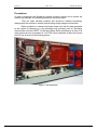
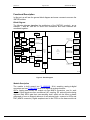
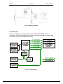
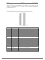
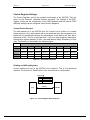
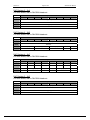
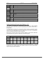
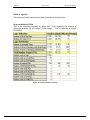
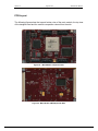
SMT350
User Manual
Version 1.9
Page 2 of 45
SMT350 User Manual
Revision History
Changes Made
Issue
Initials
11/10/05
Original Document.
1.0
PSR
18/01/06
Updates on ADC inputs and DAC outputs
(impedances)
1.1
PSR
25/01/06
Added details on PHSTR synch.
1.2
PSR
31/10/06
Dac Trigger was missing. Corrected 0x0 and 0x1C
register descriptions.
1.3
PSR
11/12/06
LED description added as well as J1 description.
1.4
PSR
25/01/2007
Connector list added; Control structure corrected.
1.5
PSR
05/02/2007
Figure 6 corrected.
1.6
PSR
21/02/2007
Scratch Test register description corrected. ADC
PLL register (0x2) corrected.
1.7
PSR
23/03/2007
Details added to the clock circuitry.
1.8
PSR
18/12/2007
Ordering Information added
1.9
PSR
Version 1.9
Page 3 of 45
SMT350 User Manual
Table of Contents
Physical Properties ....................................................................................................... 6
Ordering Information..................................................................................................... 6
Precautions................................................................................................................... 7
Introduction ................................................................................................................... 8
Overview ................................................................................................................... 8
Module features ........................................................................................................ 8
Possible applications ................................................................................................ 9
Related Documents .................................................................................................. 9
Functional Description ................................................................................................ 10
Block Diagram......................................................................................................... 10
Module Description ................................................................................................. 10
ADC Channels. ....................................................................................................... 12
ADC Main Characteristics. .................................................................................. 12
ADC Input Stage. ................................................................................................ 12
Dual-Channel DAC. ................................................................................................ 13
DAC Main characteristics. ................................................................................... 13
DAC output stage. ............................................................................................... 13
Clock Structure........................................................................................................ 14
Power Supply and Reset Structure......................................................................... 17
JumperJ1 ................................................................................................................ 17
Green LEDs. ........................................................................................................... 17
Mezzanine module Interface................................................................................... 17
Control Register Settings............................................................................................ 25
Control Packet Structure......................................................................................... 25
Reading and Writing Registers ............................................................................... 25
Memory Map ........................................................................................................... 26
Register Descriptions.............................................................................................. 27
Reset Register – 0x0........................................................................................... 27
Test Register – 0x1. ............................................................................................ 28
ADCA Register 0 – 0x2. ...................................................................................... 28
ADCA Register 1 – 0x3. ...................................................................................... 28
ADCA Register 2 – 0x4. ...................................................................................... 29
Version 1.9
Page 4 of 45
SMT350 User Manual
ADCB Register 0 – 0x5. ...................................................................................... 29
ADCB Register 1 – 0x6. ...................................................................................... 29
ADCB Register 2 – 0x7. ...................................................................................... 30
DAC Register 0 – 0x8.......................................................................................... 30
DAC Register 1 – 0x9.......................................................................................... 30
DAC Register 2 – 0xA. ........................................................................................ 31
DAC Register 3 – 0xB. ........................................................................................ 31
DAC Register 4 – 0xC. ........................................................................................ 31
DAC Register 5 – 0xD. ........................................................................................ 31
DAC Register 6 – 0xE. ........................................................................................ 32
DAC Register 7 – 0xF. ........................................................................................ 32
CDCM7005 Register 0 – 0x10. ........................................................................... 32
CDCM7005 Register 1 – 0x11. ........................................................................... 32
CDCM7005 Register 2 – 0x12. ........................................................................... 33
CDCM7005 Register 3 – 0x13. ........................................................................... 33
CDCM7005 Register 4 – 0x14. ........................................................................... 33
CDCM7005 Register 5 – 0x15. ........................................................................... 33
CDCM7005 Register 6 – 0x16. ........................................................................... 34
CDCM7005 Register 7 – 0x17. ........................................................................... 34
Main Module Temperature (not implemented) – 0x18........................................ 34
Main Module FPGA Temperature (not implemented) – 0x19 ............................. 34
Mezzanine Module Temperature (not implemented) – 0x1A.............................. 34
Mezzanine Module Converters Temperature (not implemented) – 0x1B ........... 35
Miscellaneous Register – 0x1C........................................................................... 35
Updates, Read-back and Firmware Version Registers – 0x1D .......................... 36
DDS Register 0 – Start Phase Increment LSB - 0x20 ........................................ 37
DDS Register 1 – Start Phase Increment MSB - 0x21 ....................................... 37
DDS Register 2 – Stop Phase Increment LSB - 0x22 ........................................ 38
DDS Register 3 – Stop Increment MSB - 0x23................................................... 38
DDS Register 0 – Step Phase Increment LSB - 0x24 ........................................ 38
DDS Register 5 – Step Increment MSB - 0x25................................................... 39
FPGA Design.............................................................................................................. 40
Serial Interfaces ...................................................................................................... 40
Version 1.9
Page 5 of 45
SMT350 User Manual
Block of registers .................................................................................................... 41
Space available in FPGA ........................................................................................ 41
PCB Layout................................................................................................................. 42
Connectors ................................................................................................................. 44
Description .............................................................................................................. 44
Location on the board ............................................................................................. 45
Table of Figures
Figure 1 – Fan across PCI. ......................................................................................................7
Figure 2 - Block Diagram........................................................................................................10
Figure 3 - Main features. ........................................................................................................12
Figure 4 - ADC Input Stage. ...................................................................................................12
Figure 5 - DAC Output Stage. ................................................................................................14
Figure 6 - Clock Structure. .....................................................................................................14
Figure 7 - External Clock........................................................................................................16
Figure 8 - Clock Architecture Main Characteristics. ...............................................................17
Figure 9 – Mezzanine module Connector Interface (SLB data and power connectors).........18
Figure 10 – Mezzanine Module Interface Power Connector and Pinout. ...............................20
Figure 11 – Daughter Module Interface: Data Signals Connector and Pinout (Bank A). ......21
Figure 12 – Daughter Module Interface: Data Signals Connector and Pinout (Bank B). .......23
Figure 13 – Daughter Module Interface: Data Signals Connector and Pinout (Bank C). .......24
Figure 14 – Setup Packet Structure. ......................................................................................25
Figure 15 – Control Register Read Sequence. ......................................................................25
Figure 16 – Register Memory Map.........................................................................................27
Figure 17 - Firmware Block Diagram......................................................................................40
Figure 18 - Space available in FPGA .....................................................................................41
Figure 19 – Main Module Component Side............................................................................42
Figure 20 - Main Module (SMT368) Solder Side....................................................................42
Figure 21 - Daughter Module Component Side......................................................................43
Figure 22 - Daughter Module Solder Side..............................................................................43
Figure 23 - Connectors Location. ...........................................................................................45
Version 1.9
Page 6 of 45
SMT350 User Manual
Physical Properties
Dimensions
63.5mm x 106.7mm x 18mm
Weight
35 grams
Supply Voltages
Supply Current
+12V
N/A
+5V
1.2 Amps (reset
/
converters
active)
1.4 Amps max
+3.3V
0.14 Amp (reset
/
converters
active)
0.4 Amps max
-5V
N/A
-12V
N/A
MTBF
Ordering Information
SMT350 (Standard Product): ADC inputs and DAC outputs are AC-coupled.
SMT350-DC: ADCs inputs are DC-coupled and DAC outputs are AC-coupled.
Version 1.9
Page 7 of 45
SMT350 User Manual
Precautions
In order to guarantee that Sundance’s boards function correctly and to protect the
module from damage, the following precautions should be taken:
- They are static sensitive products and should be handled accordingly.
Always place the modules in a static protective bag during storage and transition.
- When operated in a closed environment make sure that the heat generated
by the system is extracted e.g. a fan extracting heat or blowing cool air. Sundance
recommends and uses PAPST 12-Volt fans (Series 8300) producing an air flow of 54
cubic meters per hour (equivalent to 31.8 CFM). Fans are placed so they blow across
the PCI bus as show on the following picture:
Figure 1 – Fan across PCI.
Version 1.9
Page 8 of 45
SMT350 User Manual
Introduction
Overview
The SMT350 is a single width expansion TIM that plugs onto the SLB base module
SMT368 (Virtex-4 FPGA) and incorporates 2 Texas Instrument Analog-to-Digital
Converters (ADS5500) and a Texas Instrument dual-channel Digital-to-Analog
Converter (DAC5686). The SMT350 implements a comprehensive clock circuitry
based on a CDCM7005 chip that allows synchronisation among the converters and
cascading modules for multiple receiver or transmitter systems as well as the use of
an external reference clock. It provides a complete conversion solution and stands as
a platform that can be part of a transmit/receive base station.
ADCs are 14-bit and can sample at up to 125 MHz. The DAC has a resolution of 16
bits and is able to update outputs at up to 500MHz. All converters are 3.3-Volt.
The Xilinx FPGA (Virtex-4) on the base module is responsible for handling data
going/coming to/from one of the following destination/source: TI converters, Comport
(TIM-40 standard), Sundance High-speed Bus (SHB). These interfaces are
compatible with a wide range of Sundance’s modules.
The memory on base module can be divided into two 16-bit wide independent blocks
for storing incoming and/or outgoing samples.
Converter configuration, sampling and transferring modes are set via internal control
registers stored inside the FPGA and accessible via Comport.
Module features
The main features of the SMT350 are listed below:
● Dual 14-bit 125MSPS ADC (ADS5500),
● Dual channel 16-bit 500MSPS DAC (DAC5686),
● On-board low-jitter clock generation (CDCM7005),
● One external clocks, two external triggers and one reference clock via
MMCX connector,
● One SLB connector to link SMT350 and SMT368,
● Synchronisation signals,
● All Analogue inputs to be connected to 50-Ohm sources.
● All Analogue outputs to be connected to 50-Ohm loads.
● Temperature sensors.
Version 1.9
Page 9 of 45
SMT350 User Manual
Possible applications
The SMT350 can be used for the following application (this non-exhaustive list
should be taken as an example):
● High Intermediate-Frequency (IF) sampling architecture,
● Cellular base station such as CDMA and TDMA,
● Baseband I&Q systems,
● Wireless communication systems,
● Communication instrumentation,
● ...
Related Documents
ADS5500 Datasheet – Texas Instrument:
http://focus.ti.com/docs/prod/folders/print/ads5500.html
DAC5686 Datasheet – Texas Instrument:
http://focus.ti.com/docs/prod/folders/print/dac5686.html
CDCM7005 Datasheet – Texas Instrument:
http://focus.ti.com/docs/prod/folders/print/cdcm7005.html
Sundance High-speed Bus (SHB) specifications – Sundance.
ftp://ftp2.sundance.com/Pub/documentation/pdffiles/SHB_Technical_Specification.pdf
Sundance LVDS Bus (SLB) specifications – Sundance.
http://www.sundance.com/docs/SLB%20-%20Technical%20Specifications.pdf
TIM specifications.
ftp://ftp2.sundance.com/Pub/documentation/pdf-files/tim_spec_v1.01.pdf
Xilinx Virtex-4 FPGA.
http://direct.xilinx.com/bvdocs/publications/ds031.pdf
MMCX Connectors – Hubert Suhner.
MMCX Connectors
Surface Mount MMCX connector
Sundance Multiprocessor Technology Ltd.
SMT368
Version 1.9
Page 10 of 45
SMT350 User Manual
Functional Description
In this part, we will see the general block diagram and some comments on some the
SMT350 entities.
Block Diagram
The following diagram describes the architecture of the SMT350, coupled – as an
example – with an SMT368 to show how mezzanine and base modules are
connected together:
Power
Supplies: 1.8
and 3.3 Volts
Power
Supplies: 1.25,
1.5, 2.5 and 3.3
Volts
External ADC
Trigger
Temperature
Sensors
ADC Input
Ch A MMCX
50-Ohm
Channel A
Signal
Conditioning
ADS5500
ADC ChA
14-bit 125MSPS
ADC Input
Ch B MMCX
50-Ohm
Channel B
Signal
Conditioning
ADS5500
ADC ChB
14-bit 125MSPS
ChA Data(14),
Clock and Control
ChA&ChB Data, Clock
and Control (60)
ChB Data(14),
Clock and Control
ADCs and DAC External
Clock In - MMCX
Bank A
PECL Clock
Generation and
Distribution
based on
CDCM7005 and
SN65LVPC23
ADCs and DAC External
Clock Out - MMCX
External Reference
Clock Out - MMCX
DAC Clock
Daughter Card
interface
connector
DAC Output
Ch B MMCX
50-Ohm
Channel A
Signal
Conditioning
Channel B
Signal
Conditioning
DAC5686
Dual Channel DAC
16-bit 500MSPS
Interpolation
Spare SHB connector
(SHBA)
Virtex-4
XCV4SX35
Bank B
SLB
External Reference
Clock In - MMCX
DAC Output
Ch A MMCX
50-Ohm
SHBB
ADC Channel A and
Channel B
FF668 Package
2xComports and
Control (24)
Top and Bottom TIM
Connectors
448 IOs
ChA Data (16)
and Control
Spare SHB connector
(SHBC)
Bank C
ChB Data (16)
and Control
External ADC
Trigger
Power
Daughter Card
connector
ChA&ChB Data, Clock
and Control (60)
SHBD
DAC Channel A and
Channel B
SLB
SMT350
Figure 2 - Block Diagram.
Module Description
The module is built around two TI ADS5500 14-bit sampling analog-to-digital
converters and one TI DAC5686 dual 16-bit digital-to-analog converter.
ADCs: Analog data enters the module via two MMCX connectors, one for each
channel. Both signals are then conditioned (AC coupling; DC optional) before being
digitized. Both ADCs gets their own sampling clock, which can be either on-board
generated or from an external reference or an external clock, common to ADCs and
DAC (MMCX connector). Digital samples travel to the FPGA on the base module via
SMT368
Version 1.9
Page 11 of 45
SMT350 User Manual
the inter-module connector (SLB – Sundance LVDS Bus, used in this case as
‘single-ended’).
DAC: Digital samples are routed from the FPGA to the DAC via the inter-module
connector. Internal interpolation scheme allows reaching 500 Mega Samples per
Second. The DAC shows other modes such as Dual DAC, Single side-band,
Quadrature or up conversion. Both outputs are AC-coupled. By default they are
single-ended but can optionally be differential. The DAC mode is selected via Jumper
J1, that enables or disables the DAC Internal PLL (see DAC5686 datasheet for more
details).
Clock generator and distribution: All samplings clocks are generated by the same
chip. It allows having them all synchronized to a single reference clock.
Multi-module Synchronization: There are two types of synchronization available on
the SMT350. The first one is frequency synchronization, by passing the external
reference clock to an other module. It first goes through a 0-delay buffer and is then
output. Note that the synchronization is in frequency and not in phase. The second
type is register synchronization between DACs. It is achieved by the way of an extra
link between several modules to synchronize DAC internal registers (DAC signal
PHSTR passed from one module to the other and driven by the master FPGA – it
resets the internal VCO).
Inter-module Connector: it is made of a power (33 pins) and data connectors (120
pins). It is called Sundance LVDS Bus. Please refer to the SLB specifications for
more details. In the case of the SMT350, the SLB is used as ‘single-ended’.
A global reset signal is mapped to the FPGA from the bottom TIM connector.
External Clock signals, used to generate Sampling clocks. There is one external
clock, common to ADCs and DAC When used, the CDCM7005 is used as a clock
multiplexer. Also available, an external reference clock that can be passed to an
other SMT350 module with ‘0-delay’.
External Trigger: passed directly to base module. There are two, one for the ADCs
and one for the DAC.
Temperature Sensor: available for constant monitoring. Not part of default firmware
provided.
Version 1.9
Page 12 of 45
SMT350 User Manual
ADC Channels.
ADC Main Characteristics.
The main characteristics of the SMT350 ADCs are gathered into the following table.
Analogue Inputs
Input voltage range
2.4 Vp-p (11.5 dbm – 50 Ohm) Full scale AC coupled
Impedance
ADC single-ended inputs are to be
connected to a 50Ω source. Source
impedance matching implemented between
RF transformers and ADC.
Bandwidth
ADC bandwidth: 750 MHz.
ADCs Output
Output Data Width
14-Bits
2’s Compliment or offset binary
Data Format
(Changeable via control register)
SFDR
82dBs maximum (manufacturer)
SNR
70dBs maximum (manufacturer)
Minimum Sampling Clock
10 MHz (ADC DLL off)
Maximum Sampling Frequency
125 MHz (ADC DLL on)
Figure 3 - Main features.
ADC Input Stage.
Each ADC Analogue input is AC-coupled via and RF transformer. The 50-Ohm
resistor between the connector and the first RF transformer is not fitted because the
source impedance match is implemented between the second RF transformer and
the ADC by the way of two 25-Ohm resistors.
Figure 4 - ADC Input Stage.
Version 1.9
Page 13 of 45
SMT350 User Manual
Dual-Channel DAC.
DAC Main characteristics.
The main characteristics of the SMT350 DAC are gathered into the following table.
Analogue Outputs
Input voltage range
1 Vp-p – Full scale - AC coupled
Impedance
DAC single-ended outputs are to be
connected to a 50Ω load, which impedance
matching implemented between DAC and
RF transformers.
Bandwidth
TBD
DAC Input
Output Data Width per channel
Data Format
16-Bits
2’s Compliment or offset binary
(Changeable via control register)
SFDR
89dBs maximum (manufacturer)
SNR
80dBs maximum (manufacturer)
Maximum input data rate
160 MSPS (Clk1 – DAC5686)
Maximum Sampling rate
500 MSPS (Clk2 – DAC5686)
Jumper J1 disables (position 1-2; also called External Clock Mode) or enables
(position2-3; also called Internal Clock Mode) the DAC internal PLL.
DAC output stage.
The following piece of schematics shows how the DAC outputs are coupled. The
DAC5686 generates differential output signals that are fed into an RF transformer
(Ohm ratio 4), that makes both DAC channels AC coupled. 100-Ohm resistors to Vcc
on the primary stage of the transformer allow balancing the secondary stage to 50
Ohm single-ended. (Note that R153 is not mounted).
Version 1.9
Page 14 of 45
SMT350 User Manual
Figure 5 - DAC Output Stage.
Clock Structure
There is one integrated clock generator on the module (CDCM7005 – Texas
instrument). The user can either use this clock (on-board) or provide the module with
an external clock (input via MMCX connector).
Figure 6 - Clock Structure.
Version 1.9
Page 15 of 45
SMT350 User Manual
ADCs can both receive the same clock or the fraction of the CDCM7005 input clock
(/2, /3, /4, /6, /8 or /16), the maximum being 125MHz for each ADC. This input clock
can be coming from the on-board fixed VCXO or from an external source. Here is a
list of possible sampling frequencies for the ADCs:
ADC Sampling
Frequency
CDCM7005 Setting
Clock source
Not Allowed
/1
On-board VCXO (fixed
245.76MHz)
122.88 MHz
/2
On-board VCXO (fixed
245.76MHz)
81.92 MHz
/3
On-board VCXO (fixed
245.76MHz)
61.44 MHz
/4
On-board VCXO (fixed
245.76MHz)
40.96 MHz
/6
On-board VCXO (fixed
245.76MHz)
30.72 MHz
/8
On-board VCXO (fixed
245.76MHz)
15.36 MHz
/16
On-board VCXO (fixed
245.76MHz)
Anything between 10
and 125 MHz
/1, /2, /3, /4, /6, /8 or
/16
External Clock
The same applies to the DAC, with a maximum sampling frequency for clk1 of
160MHz and for clk2 of 500Mhz.
Below is shown how the external clock is fed to the system. By default it is singleended and AC-coupled before being converted into LVPECL format. The option of
having a differential external clock is still possible on the hardware by the way of
fitting or not some of the components.
Version 1.9
Page 16 of 45
SMT350 User Manual
Figure 7 - External Clock.
The main characteristics of the SMT350 Clocks are gathered into the following table.
External Reference Input
Input Voltage Level
0.5 – 3.3 Volts peak-to-peak (AC-coupled)
Input Impedance
50-Ohm (Termination implemented at the
connector)
Frequency Range
0 – 100 MHz.
External Reference Output
Output Voltage Level
1.6 Volts peak-to-peak (AC-coupled)
Output Impedance
50-Ohm (Termination implemented at the
connector)
External Sampling Clock Input
Input Voltage Level
0.5 – 3.3 Volts peak-to-peak (AC-coupled)
Input Format
Single-ended or differential on option (3.3V
LVPECL).
Frequency range
10-500 MHz
External Sampling Clock Output
Output Voltage Level
0-2.4 Volts fixed amplitude
Output Format
LVTTL
External Trigger Inputs
Input Voltage Level
1.5-3.3 Volts peak-to-peak.
Format
DC-coupled and Single-ended (Termination
implemented at the connector). Differential
Version 1.9
Page 17 of 45
SMT350 User Manual
on option (3.3 V PECL).
Impedance
50-Ohm.
Frequency range
62.5 MHz maximum
Delay
External Ref. Input to Ext Ref. Out
External Clk Input to Ext Clk Out
9ns (between J29 and J4)
Figure 8 - Clock Architecture Main Characteristics.
Power Supply and Reset Structure
The SMT350 gets two power sources from the base module: 3.3 and 5 Volts. Linear
regulators are used to provide a clean and stable voltage supply to the analog
converters.
JumperJ1
There is one jumper (3 pin header) on the board. It is to control the power supply of
the DAC internal PLL. When fitted on positions 2 and 3, the PLL is enabled, whereas
on positions 1 and 2, it is disabled. Please refer to the DAC5686 datasheet for more
details.
Green LEDs.
There are 7 LEDs on the SMT350 Daughter Module. Five are dedicated for power
supplies monitoring: LED1 (1.8V DAC), LED2 (3.3V Clock), LED3 (3.3V DAC), LED4
(3.3V ADCA), LED6 (3.3V ADCB) should be all ON when the board is under power.
They state that power supplies all work fine.
LED5 (ADCs) should be flashing once the ADC Clocks are set up. It is actually a
divided version of ADCA sampling clock). LED7 (DAC) is a divided version of
PLLLOCK coming from the Dac (DAC5686).
Mezzanine module Interface
The daughter module interface is made up of two connectors (data and power). The
first one is a 0.5mm-pitch differential Samtec connector. This connector is for
transferring data such as ADC or DAC samples to and from the FPGA on the main
module. The second one is a 1mm-pitch Samtec header type connector. This
connector is for providing power to the daughter-card.
Sundance defines these two connectors as the Sundance LVDS Bus (SLB). It has
originally been made for data transfers using LVDS format but can also be used with
single-ended lines, which is the case for the SMT350. To know more about the SLB,
please refer to the SLB specifications.
Version 1.9
Page 18 of 45
SMT350 User Manual
The figure underneath illustrates this configuration. The bottom view of the daughter
card is shown on the right. This view must the mirrored to understand how it connects
to the main module.
Data
connectors
Bank A
Bank B
Bank C
Power
connectors
Figure 9 – Mezzanine module Connector Interface (SLB data and power connectors).
The female differential connector is located on the base module. The Samtec Part
Number for this connector is QTH-060-01-F-D-DP-A.
The female power connector is located on the base module. The Samtec Part
Number for this connector is BKS-133-03-F-V-A
The male differential connector is located on the mezzanine card. The Samtec Part
Number for this connector is QSH-060-01-F-D-DP-A
The male power connector is located on the mezzanine card. The Samtec Part
Number for this connector is BKT-133-03-F-V-A
The mated height between the main module and the daughter card is 5 mm.
Version 1.9
Page 19 of 45
SMT350 User Manual
Some JTAG Lines are also mapped onto this connector to be used in case the
Daughter module would have a TI Processor. They would allow debugging and
programming via JTAG.
The following table shows the pin assignment on the power connector:
2
1
33
Pin Number
Pin Name
Description of Signal
1
D+3V3
Digital 3.3 Volts
2
DGND
Digital Ground
3
D+3V3
Digital 3.3 Volts
4
DGND
Digital Ground
5
D+3V3
Digital 3.3 Volts
6
DGND
Digital Ground
7
D+3V3
Digital 3.3 Volts
8
DGND
Digital Ground
9
D+5V0
Digital 5.0 Volts
10
DGND
Digital Ground
11
D+5V0
Digital 5.0 Volts
12
DGND
Digital Ground
13
D+5V0
Digital 5.0 Volts
14
DGND
Digital Ground
15
D+5V0
Digital 5.0 Volts
16
DGND
Digital Ground
17
D+12V0
Digital +12.0 Volts – not used on the SMT350
18
DGND
Digital Ground
19
D+12V0
Digital +12.0 Volts – not used on the SMT350
20
DGND
Digital Ground
Version 1.9
21
Page 20 of 45
D-12V0
Digital –12.0 Volts – not used on the SMT350
22
DGND
Digital Ground
23
D-12V0
Digital –12.0 Volts – not used on the SM350
24
DGND
Digital Ground
25
DGND
Digital Ground
26
EMU0
Emulation Control 0 – not used on SMT350
27
EMU1
Emulation Control 1 – not used on SMT350
28
TMS
JTAG Mode Control – not used on SMT350
29
nTRST
JTAG Reset – not used on SMT350
30
TCK
JTAG Test Clock – not used on SMT350
31
TDI
JTAG Test Input – not used on SMT350
32
TDO
JTAG Test Output – not used on SMT350
33
DGND
Digital Ground
SMT350 User Manual
Figure 10 – Mezzanine Module Interface Power Connector and Pinout.
The following few pages describes the signals on the data connector between the
main module and the daughter card. Bank A on the connector is used for the ADC
Channels A and B. Bank C is used for the DAC channels A and B. Bank B is used for
system clock and trigger signals, ADC/DAC/Clock control signal.
Version 1.9
Page 21 of 45
Bank A
SMT350 User Manual
Bank B
13 57
Bank C
41 43
81 83
24 68
Bank A (ADCs)
Pin No
Pin Name
Signal Description
Pin No
Pin Name
Signal Description
Dir
Daughter Card to Main Module
Dir
Daughter Card to Main Module
1
DOAI0p
Data Out 0, Channel A.
2
DOBI0p
Data Out 1, Channel A.
3
DOAI0n
Data Out 2, Channel A.
4
DOBI0n
Data Out 3, Channel A.
Dir
Daughter Card to Main Module
Dir
Daughter Card to Main Module
5
DOAI1p
Data Out 4, Channel A.
6
DOBI1p
Data Out 5, Channel A.
7
DOAI1n
Data Out 6, Channel A.
8
DOBI1n
Data Out 7, Channel A.
Dir
Daughter Card to Main Module
Dir
Daughter Card to Main Module
9
DOAI2p
Data Out 8, Channel A.
10
DOBI2p
Data Out 9, Channel A.
11
DOAI2n
Data Out 10, Channel A.
12
DOBI2n
Data Out 11, Channel A.
Dir
Daughter Card to Main Module
Dir
Daughter Card to Main Module
13
DOAI3p
Data Out 12, Channel A.
14
DOBI3p
Data Out 13, Channel A.
15
DOAI3n
Over Range, Channel A.
16
DOBI3n
Data Out 0, Channel B.
Dir
Daughter Card to Main Module
Dir
Daughter Card to Main Module
17
DOAI4p
Data Out 1, Channel B.
18
DOBI4p
Data Out 2, Channel B.
19
DOAI4n
Data Out 3, Channel B.
20
DOBI4n
Data Out 4, Channel B.
Dir
Daughter Card to Main Module
Dir
Daughter Card to Main Module
21
DOAI5p
Data Out 5, Channel B.
22
DOBI5p
Data Out 6, Channel B.
23
DOAI5n
Data Out 7, Channel B.
24
DOBI5n
Data Out 8, Channel B.
Dir
Daughter Card to Main Module
Dir
Daughter Card to Main Module
25
DOAI6p
Data Out 9, Channel B.
26
DOBI6p
Data Out 10, Channel B.
27
DOAI6n
Data Out 11, Channel B.
28
DOBI6n
Data Out 12, Channel B.
Dir
Daughter Card to Main Module
Dir
Daughter Card to Main Module
29
DOAI7p
Data Out 13, Channel B.
30
DOBI7p
Over Range, Channel B.
31
DOAI7n
Led ADC
32
DOBI7n
Status Lock CDCM7005
Dir
Daughter Card to Main Module
Dir
Daughter Card to Main Module
33
ClkOIp
Data Clock Out, Channel A.
34
DOIRIp
Status VCXO CDCM7005
35
ClkOIn
Data Clock Out, Channel B.
Status Ref CDCM7005
Dir
Reserved.
37
Reserved.
39
Reserved.
36
DOIRIn
Dir
Reserved.
Reserved.
38
Reserved
ADC External Trigger, P.
Reserved.
40
Reserved
ADC External Trigger, N.
Figure 11 – Daughter Module Interface: Data Signals Connector and Pinout (Bank A).
Version 1.9
Page 22 of 45
Bank A
SMT350 User Manual
Bank B
13 57
Bank C
41 43
81 83
24 68
Bank B
Pin No
Pin Name
Type
Dir
Signal Description
Pin No
Pin Name
Signal Description
Clock and Trigger System Signals
Type
Clock and Trigger System Signals
Daughter Card to Main Module
Dir
Daughter Card to Main Module
41
SMBClk
Temperature Sensor Clock.
42
SMBData
Temperature Sensor Data.
43
SMBnAlert
Temperature Sensor Alert.
44
SerialNo
Reserved
Dir
Daughter Card to Main Module
Dir
Reserved
45
AdcVDacI
Reserved
46
AdcVDacQ
Reserved
47
AdcVRes
Reserved
48
AdcReset
Reserved
Dir
Main Module to Daughter Card
Dir
Main Module to Daughter Card
49
D3v3Enable
Reserved
50
D2v5Enable
Reserved
51
AdcMode
ADCA Serial Clock.
52
AdcClock
ADCA Serial Data.
Type
ADC Specific Signals
Type
ADC Specific Signals
Dir
Main Module to Daughter Card
Dir
Reserved
53
AdcLoad
ADCA Serial Enable.
54
AdcData
ADCB Serial Clock.
55
AdcCal
ADCB Serial Data.
56
AdjClkCntr0
ADCB Serial Enable.
Dir
Main Module to Daughter Card
Dir
Main Module to Daughter Card
57
AdjClkCntr1
ADCs Format (binary, 2’s)
58
AdjClkCntr2
ADCs Reset
59
AdjClkCntr3
ADCs Output Enable
60
PllCntr0
CDCM7005 serial Enable.
Dir
Daughter Card to Main Module
Dir
Daughter Card to Main Module
61
PllCntr1
CDCM7005 serial Clock.
62
PllCntr2
CDCM7005 serial Data.
63
PllCntr3
CDCM7005 Clock Selection.
64
AdcAClkSel
DAC PhStr.
Type
Module Control Signals
Type
Module Control Signals
Dir
Main Module to Daughter Card
Dir
Main Module to Daughter Card
65
AdcBClkSel
DAC Reset.
66
IntClkDivEn
DAC Pll Lock.
67
IntClkDivnReset
DAC Serial Enable.
68
IntExtClkDivEn
DAC Serial Clock.
Dir
Main Module to Daughter Card
Dir
Main Module to Daughter Card
69
IntExtClkDivnReset
DAC Serial Data.
70
FpgaVRef
Reserved
71
FpgaTck
Reserved
72
FpgaTms
Reserved
Dir
Daughter Card to Main Module
Dir
Reserved
73
FpgaTdi
Reserved
74
FpgaTdo
Reserved
75
MspVRef
Reserved
76
MspTck
Reserved
Dir
Daughter Card to Main Module
Dir
Reserved
Version 1.9
Page 23 of 45
SMT350 User Manual
77
MspTms
Reserved
78
MspTdi
Reserved.
79
Msptdo
Reserved
80
MspnTrst
Reserved
Figure 12 – Daughter Module Interface: Data Signals Connector and Pinout (Bank B).
Version 1.9
Page 24 of 45
Bank A
SMT350 User Manual
Bank B
13 57
Bank C
41 43
81 83
24 68
Bank C (DAC)
Pin No
Pin Name
Signal Description
Pin No
Pin Name
Signal Description
Dir
Daughter Card to Main Module
Dir
Daughter Card to Main Module
81
DOAQ0p
Data In 0, Channel A.
82
DOBQ0p
Data In 1, Channel A.
83
DOAQ0n
Data In 2, Channel A.
84
DOBQ0n
Data In 3, Channel A.
Dir
Daughter Card to Main Module
Dir
Daughter Card to Main Module
85
DOAQ1p
Data In 4, Channel A.
86
DOBQ1p
Data In 5, Channel A.
87
DOAQ1n
Data In 6, Channel A.
88
DOBQ1n
Data In 7, Channel A.
Dir
Daughter Card to Main Module
Dir
Daughter Card to Main Module
89
DOAQ2p
Data In 8, Channel A.
90
DOBQ2p
Data In 9, Channel A.
91
DOAQ2n
Data In 10, Channel A.
92
DOBQ2n
Data In 11, Channel A.
Dir
Daughter Card to Main Module
Dir
Daughter Card to Main Module
93
DOAQ3p
Data In 12, Channel A.
94
DOBQ3p
Data In 13, Channel A.
95
DOAQ3n
Data In 14, Channel A.
96
DOBQ3n
Data In 15, Channel A.
Dir
Daughter Card to Main Module
Dir
Daughter Card to Main Module
97
DOAQ4p
Data In 0, Channel B.
98
DOBQ4p
Data In 1, Channel B.
99
DOAQ4n
Data In 2, Channel B.
100
DOBQ4n
Data In 3, Channel B.
Dir
Daughter Card to Main Module
Dir
Daughter Card to Main Module
101
DOAQ5p
Data In 4, Channel B.
102
DOBQ5p
Data In 5, Channel B.
103
DOAQ5n
Data In 6, Channel B.
104
DOBQ5n
Data In 7, Channel B.
Dir
Daughter Card to Main Module
Dir
Daughter Card to Main Module
105
DOAQ6p
Data In 8, Channel B.
106
DOBQ6p
Data In 9, Channel B.
107
DOAQ6n
Data In 10, Channel B.
108
DOBQ6n
Data In 11, Channel B.
Dir
Daughter Card to Main Module
Dir
Daughter Card to Main Module
109
DOAQ7p
Data Out 12, Channel B.
110
DOBQ7p
Data Out 13, Channel B.
111
DOAQ7n
Data Out 14, Channel B.
112
DOBQ7n
Data Out 15, Channel B.
Dir
Daughter Card to Main Module
Dir
Daughter Card to Main Module
113
Reserved.
DAC Clock P.
114
Reserved.
DAC LED.
115
Reserved.
DAC Clock N.
116
Reserved.
DAC Power Down.
Dir
Reserved.
Dir
Reserved.
117
Reserved.
Reserved.
118
Reserved.
DAC External Trigger, P.
119
Reserved.
Reserved.
120
Reserved.
DAC External Trigger, N.
Figure 13 – Daughter Module Interface: Data Signals Connector and Pinout (Bank C).
Version 1.9
Page 25 of 45
SMT350 User Manual
Control Register Settings
The Control Registers control the complete functionality of the SMT350. They are
setup via the Comport3 (standard firmware provided). The settings of the ADC,
triggers, clocks and the configuration of the SHB interfaces and the internal FPGA
data path settings can be configured via the Control Registers.
Control Packet Structure
The data passed on to the SMT350 over the Comport must conform to a certain
packet structure. Only valid packets will be accepted and only after acceptance of a
packet will the appropriate settings be implemented. Each packet will start with a
command (4 bits – 0x1 for a write operation – 0x2 for a read operation) information,
followed by a register address (12 bits – see table Memory Map), followed by a 16-bit
data. This structure is illustrated in the following figure:
Byte Content
Byte
Bit 7
Bit 6
Bit 5
Bit 4
Bit 3
Bit 2
Bit 1
Bit 0
3
Command
3
Command
2
Command
1
Command
0
Address 11
Address 10
Address 9
Address 8
2
Address 7
Address 6
Address 5
Address 4
Address 3
Address 2
Address 1
Address 0
1
Data 15
Data 14
Data 13
Data 12
Data 11
Data 10
Data 9
Data 8
0
Data 7
Data 6
Data 5
Data 4
Data 3
Data 2
Data 1
Data 0
Figure 14 – Setup Packet Structure.
Reading and Writing Registers
Control packets are sent to the SMT350 over Comport3. This is a bi-directional
interface. The format of a ‘Read Packet’ is the same as that of a write packet.
Figure 15 – Control Register Read Sequence.
Version 1.9
Page 26 of 45
SMT350 User Manual
Memory Map
The write packets must contain the address where the data must be written to and
the read packets must contain the address where the required data must be read.
The following figure shows the memory map for the writable and readable Control
Registers on the SMT350:
Address
Writable Registers
Readable Registers
0x00
Reset Register.
Reserved.
0x01
Test Register.
Test Register.
0x02
ADCA Register 0.
Read-back (FPGA Register) ADCA Register 0.
0x03
ADCA Register 1.
Read-back (FPGA Register) ADCA Register 1.
0x04
ADCA Register 2.
Read-back (FPGA Register) ADCA Register 2.
0x05
ADCB Register 0.
Read-back (FPGA Register) ADCB Register 0.
0x06
ADCB Register 1.
Read-back (FPGA Register) ADCB Register 1.
0x07
ADCB Register 2.
Read-back (FPGA Register) ADCB Register 2.
0x08
DAC Register 0.
Read-back (FPGA Register) DAC Register 0.
0x09
DAC Register 1.
Read-back (FPGA Register) DAC Register 1.
0x0A
DAC Register 2.
Read-back (FPGA Register) DAC Register 2.
0x0B
DAC Register 3.
Read-back (FPGA Register) DAC Register 3.
0x0C
DAC Register 4.
Read-back (FPGA Register) DAC Register 4.
0x0D
DAC Register 5.
Read-back (FPGA Register) DAC Register 5.
0x0E
DAC Register 6.
Read-back (FPGA Register) DAC Register 6.
0x0F
DAC Register 7.
Read-back (FPGA Register) DAC Register 7.
0x10
CDCM7005 Register 0.
Read-back (FPGA Register) CDCM7005 Register 0.
0x11
CDCM7005 Register 1.
Read-back (FPGA Register) CDCM7005 Register 1.
0x12
CDCM7005 Register 2.
Read-back (FPGA Register) CDCM7005 Register 2.
0x13
CDCM7005 Register 3.
Read-back (FPGA Register) CDCM7005 Register 3.
0x14
CDCM7005 Register 4.
Read-back (FPGA Register) CDCM7005 Register 4.
0x15
CDCM7005 Register 5.
Read-back (FPGA Register) CDCM7005 Register 5.
0x16
CDCM7005 Register 6.
Read-back (FPGA Register) CDCM7005 Register 6.
0x17
CDCM7005 Register 7.
Read-back (FPGA Register) CDCM7005 Register 7.
0x18
Reserved
Main Module Temperature
0x19
Reserved
Main Module FPGA Temperature
0x1A
Reserved
Mezzanine Module Temperature
0x1B
Reserved
Mezzanine Module Converter Temperature
0x1C
Misc Register (Trigger, Clock Selection, etc…).
Read-back Misc Register.
0x1D
Update and Read-back command Register
Firmware Version and Status bits.
0x20
DDS Register 0 – Start Phase Increment LSB
Read-back (FPGA Register) DDS Register 0.
0x21
DDS Register 1 – Start Phase Increment MSB
Read-back (FPGA Register) DDS Register 1.
0x22
DDS Register 2 – Stop Phase Increment LSB
Read-back (FPGA Register) DDS Register 2.
0x23
DDS Register 3 – Stop Phase Increment MSB
Read-back (FPGA Register) DDS Register 3.
Version 1.9
Page 27 of 45
SMT350 User Manual
0x24
DDS Register 4 – Step Phase Increment LSB
Read-back (FPGA Register) DDS Register 4.
0x25
DDS Register 5 – Step Phase Increment MSB
Read-back (FPGA Register) DDS Register 5.
Figure 16 – Register Memory Map.
Register Descriptions
Reset Register – 0x0.
Reset Register – 0x0
Byte
Bit 7
Bit 6
Bit 5
0
Reserved
Reserved
DDS
Reset
Default
‘0’
‘0’
‘1’
Bit 4
Bit 3
Bit 2
Bit 1
Bit 0
PHSTR
CDCM7005
Reset
DAC Reset
ADCs
Reset
‘00’
‘1’
‘1’
‘1’
Reset Register – 0x0
Setting
Bit 0
Description
0
0
Normal Operation.
1
1
Resets both ADC devices as well as their corresponding Serial Interfaces.
Setting
Bit 1
0
0
Normal Operation.
1
1
Resets both DAC device as well as its Serial Interfaces.
Setting
Bit 2
0
0
Normal Operation.
1
1
Resets both CLK device as well as its Serial Interfaces.
Setting
Bit 4&3
0
00
Normal Operation – DAC PHSTR is Tri-Stated.
1
01
DAC PHSTR line is driven High.
2
10
DAC PHSTR line is driven Low.
3
11
Normal Operation – DAC PHSTR is Tri-Stated.
Setting
Bit 5
0
0
DDS Activated and SHB put on hold.
1
1
Resets DDS Core (SHB samples are routed to the DAC)
Description
Description
Description
Description
Note 1: What is mentioned as DAC PHSTR line is the physical net on the board that
connects together the FPGA to the PHSTR pin (DAC5686) as well as to J5 (+). In a
multiple board system, one board can be used as a master and its PHSTR pin can
be driven high or low and an other one as slave, in which case its DAC PHSTR pin
must be tri-stated.
Note 2: The Reset bits don’t get cleared automatically, so a device can remain reset
while not used to reduce the global power consumption.
Version 1.9
Page 28 of 45
SMT350 User Manual
Test Register – 0x1.
Any 8-bit value written in this register can be read-back to check that the Comport
used works properly.
Test Register – 0x1
Byte
Bit 7
Bit 6
Bit 5
Bit 4
Bit 3
Bit 2
Bit 1
Bit 0
Bit 2
Bit 1
Bit 0
0
ADCA Register 0 – 0x2.
For more details, refer to ADS5500 datasheet.
ADCA Register 0 – 0x2
Byte
Bit 7
Bit 6
Bit 5
Bit 4
Bit 3
1
Reserved
Default
‘0000000’
0
Reserved
PLL
Reserved
Default
‘000000’
‘0’
‘0’
Bit 2
Bit 1
Bit 0
TP1
TP0
Reserved
‘0’
‘0’
‘0’
ADCA Register 0 – 0x2
Setting
Bit 1
Description
0
0
PLL OFF – for sampling frequencies between 10 and 80 MHz
1
1
PLL ON – for sampling frequencies between 60 and 125 MHz
ADCA Register 1 – 0x3.
For more details, refer to ADS5500 datasheet.
ADCA Register 1 – 0x3
Byte
Bit 7
Bit 6
Bit 5
Bit 4
1
Reserved
Default
‘00000’
Bit 3
0
Reserved
Default
‘00000000’
ADCA Register 1 – 0x3
Setting
TP1
TP0
Description
0
0
0
Normal Mode of Operation
1
0
1
All outputs are zeroes
2
1
0
All outputs are ones
3
1
1
Continuous stream of ‘10’
Version 1.9
Page 29 of 45
SMT350 User Manual
ADCA Register 2 – 0x4.
For more details, refer to ADS5500 datasheet.
ADCA Register 2 – 0x4
Byte
Bit 7
Bit 6
Bit 5
1
Reserved
Default
‘000’
Bit 4
Bit 3
Bit 2
Bit 1
PDN
Reserved
‘0’
‘000’
0
Reserved
Default
‘00000000’
Bit 0
ADCA Register 2 – 0X4
Setting
PDN
Description
0
0
Normal Mode of Operation
1
1
Device in Power Down Mode
ADCB Register 0 – 0x5.
For more details, refer to ADS5500 datasheet.
ADCB Register 0 – 0x5
Byte
Bit 7
Bit 6
Bit 5
Bit 4
Bit 3
1
Reserved
Default
‘0000000’
Bit 2
Bit 1
Bit 0
0
Reserved
PLL
Reserved
Default
‘000000’
‘0’
‘0’
ADCB Register 0 – 0x5
Setting
Bit 1
0
0
PLL OFF – for sampling frequencies between 10 and 80 MHz
Description
1
1
PLL ON – for sampling frequencies between 60 and 125 MHz
ADCB Register 1 – 0x6.
For more details, refer to ADS5500 datasheet.
ADCB Register 1 – 0x6
Byte
Bit 2
Bit 1
Bit 0
1
Bit 7
Bit 6
Reserved
Bit 5
Bit 4
Bit 3
TP1
TP0
Reserved
Default
‘00000’
‘0’
‘0’
‘0’
0
Reserved
Default
‘00000000’
ADCB Register 1 – 0x6
Setting
TP1
0
0
TP0
0
Description
Normal Mode of Operation
Version 1.9
Page 30 of 45
1
0
1
2
1
0
All outputs are ones
3
1
1
Continuous stream of ‘10’
SMT350 User Manual
All outputs are zeroes
ADCB Register 2 – 0x7.
For more details, refer to ADS5500 datasheet.
ADCB Register 2 – 0x7
Byte
Bit 7
Bit 6
Bit 5
Bit 4
Bit 3
Bit 2
Bit 1
1
Reserved
PDN
Reserved
Default
‘000’
‘0’
‘000’
0
Reserved
Default
‘00000000’
Bit 0
ADCB Register 2 – 0x7
Setting
PDN
0
0
Normal Mode of Operation
Description
1
1
Device in Power Down Mode
DAC Register 0 – 0x8.
For more details, refer to DAC5686 datasheet.
DAC Register 0 – 0x8
Byte
Bit 7
Bit 6
Bit 5
0
atest
Default
‘000000’
Bit 4
Bit 3
Bit 2
Bit 1
Bit 0
Version
‘000’
1
Freq_int[7:0]
Default
‘00000000’
DAC Register 1 – 0x9.
For more details, refer to DAC5686 datasheet.
DAC Register 1 – 0x9
Byte
Bit 7
Bit 6
Bit 5
Bit 4
Bit 3
0
Freq_int[15:8]
Default
‘00000000’
1
Freq_int[23:16]
Default
‘00000000’
Bit 2
Bit 1
Bit 0
Version 1.9
Page 31 of 45
SMT350 User Manual
DAC Register 2 – 0xA.
For more details, refer to DAC5686 datasheet.
DAC Register 2 – 0xA
Byte
Bit 7
Bit 6
Bit 5
Bit 4
Bit 3
Bit 2
Bit 1
Bit 0
Bit 2
Bit 1
Bit 0
Freq_int[31:24]
0
Default
‘00000000’
1
Phase_int[7:0]
Default
‘00000000’
DAC Register 3 – 0xB.
For more details, refer to DAC5686 datasheet.
DAC Register 3 – 0xB
Byte
Bit 7
Bit 6
Bit 5
Bit 4
Bit 3
Phase _int[15:8]
0
‘00000000’
Default
1
Mode[1:0]
Div[1:0]
Sel[1:0]
Counter
Full bypass
Default
‘00’
‘00’
‘00’
‘0’
‘0’
DAC Register 4 – 0xC.
For more details, refer to DAC5686 datasheet.
DAC Register 4 – 0xC
Byte
Bit 7
Bit 6
Bit 5
Bit 4
Bit 3
Bit 2
Bit 1
Bit 0
0
Ssb
Interl
Sinc
Dith
Sync Phstr
Nco
Sif4
Twos
Default
‘0’
‘0’
‘0’
‘0’
‘0’
‘0’
‘0’
‘0’
1
Dual_clk
DSS_gain[1:0]
Rspect
Qflag
Pll_rng[1:0]
Rev_bus
Default
‘0’
‘00’
‘0’
‘0’
‘00’
‘0’
DAC Register 5 – 0xD.
For more details, refer to DAC5686 datasheet.
DAC Register 5 – 0xD
Byte
Bit 7
Bit 6
Bit 5
Bit 4
Bit 3
0
Daca_offset[7:0]
Default
‘00000000’
1
Daca_gain[7:0]
Default
‘00000000’
Bit 2
Bit 1
Bit 0
Version 1.9
Page 32 of 45
SMT350 User Manual
DAC Register 6 – 0xE.
For more details, refer to DAC5686 datasheet.
DAC Register 6 – 0xE
Byte
Bit 7
Bit 6
Bit 5
Bit 4
Daca_offset[10:8]
0
Bit 3
Bit 2
Bit 1
sleepa
Daca_gain[11:8]
‘0’
‘0000’
Default
1
Dacb_offset[7:0]
Default
‘00000000’
Bit 0
DAC Register 7 – 0xF.
For more details, refer to DAC5686 datasheet.
DAC Register 7 – 0xF
Byte
Bit 7
Bit 6
Bit 5
Bit 4
Bit 3
Bit 2
Bit 1
Bit 0
Dacb_gain[7:0]
0
‘00000000’
Default
1
Dacb_offset[10:8]
sleepb
Dacb_gain[11:8]
Default
‘000’
‘0’
‘0000’
CDCM7005 Register 0 – 0x10.
For more details, refer to CDCM7005 datasheet.
CDCM7005 Register 0 – 0x10
Byte
Bit 7
Bit 6
Bit 5
Bit 4
Bit 3
Bit 2
Bit 1
1
VCXO_divider[3:0]
Reference Divider[9:6]
Default
‘0000’
‘0000’
Bit 0
0
Reference Divider[5:0]
Register Selection[1:0]
Default
‘000000’
‘00’
CDCM7005 Register 1 – 0x11.
For more details, refer to CDCM7005 datasheet.
CDCM7005 Register 1 – 0x11
Byte
Bit 7
Bit 6
Bit 5
Bit 4
1
Freq Detect
Manual or Auto
Ref.
Programmable Delay N[2:0]
Programmable Delay M[2:0]
Default
‘0’
‘0’
‘000’
‘000’
0
VCXO_divider[11:4]
Default
‘00000000’
Bit 3
Bit 2
Bit 1
Bit 0
Version 1.9
Page 33 of 45
SMT350 User Manual
CDCM7005 Register 2 – 0x12.
For more details, refer to CDCM7005 datasheet.
CDCM7005 Register 2 – 0x12
Byte
Bit 7
Bit 6
Bit 5
Bit 4
Bit 3
Bit 2
Bit 1
Bit 0
1
OUT2A0
OUT1B1
OUT1B0
OUT1A1
OUT1A0
OUT0B1
OUT0B0
OUT0A1
Default
‘0’
‘0’
‘0’
‘0’
‘0’
‘0’
‘0’
‘0’
0
OUT0A0
Output Signaling Selcetion[5:0]
Register Selection[1:0]
Default
‘0’
‘00000’
‘01’
CDCM7005 Register 3 – 0x13.
For more details, refer to CDCM7005 datasheet.
CDCM7005 Register 3– 0x13
Byte
Bit 7
Bit 6
Bit 5
Bit 4
Bit 3
Bit 2
Bit 1
Bit 0
1
90Div8
90Div4
ADClock
Status
VCXO
Status Ref
OUT4B1
OUT4B0
OUT4A1
Default
‘0’
‘0’
‘0’
‘0’
‘0’
‘0’
‘0’
‘0’
0
OUT4A0
OUT3B1
OUT3B0
OUT3A1
OUT3A0
OUT2B1
OUT2B0
OUT2A1
Default
‘0’
‘0’
‘0’
‘0’
‘0’
‘0’
‘0’
‘0’
CDCM7005 Register 4 – 0x14.
For more details, refer to CDCM7005 datasheet.
CDCM7005 Register 4 – 0x14
Byte
Bit 7
Bit 6
Bit 5
Bit 4
Bit 3
Bit 2
Bit 1
Bit 0
1
Y0_MUX
Width FB_MUX
PDF Pulse
Default
‘000’
‘000’
‘00’
0
CP Current
PRECP
CP_DIR
Register Selection[1:0]
Default
‘0000’
‘0’
‘0’
‘10’
CDCM7005 Register 5 – 0x15.
For more details, refer to CDCM7005 datasheet.
CDCM7005 Register 5– 0x15
Byte
Bit 7
Bit 6
Bit 5
Bit 4
Bit 3
Bit 2
1
Hold
Reset
ResHold
Power
Down
Y4_MUX
Default
‘0’
‘0’
‘0’
‘0’
‘000’
Bit 1
Bit 0
Y3_MUX
‘0’
0
Y3_MUX
Y2_MUX
Y1_MUX
Default
‘00’
‘000’
‘000’
Version 1.9
Page 34 of 45
SMT350 User Manual
CDCM7005 Register 6 – 0x16.
For more details, refer to CDCM7005 datasheet.
CDCM7005 Register 6 – 0x16
Byte
Bit 7
Bit 6
Bit 5
Bit 4
Reserved
1
‘0000’
Default
Bit 3
Bit 2
Bit 1
Bit 0
Hold
Reserved
Hold
Function1
Reserved
‘0’
‘0’
‘0’
‘0’
0
Reserved
Cycle Slip
Lock Cycles
Lock Window
Register Selection[1:0]
Default
‘0’
‘0’
‘00’
‘00’
‘11’
CDCM7005 Register 7 – 0x17.
For more details, refer to CDCM7005 datasheet.
CDCM7005 Register 7 – 0x17
Byte
Bit 7
Bit 6
Bit 5
Bit 4
1
Reserved
Default
‘00000000’
0
Reserved
Default
‘00000000’
Bit 3
Bit 2
Bit 1
Bit 0
Bit 2
Bit 1
Bit 0
Bit 2
Bit 1
Bit 0
Bit 2
Bit 1
Bit 0
Main Module Temperature (not implemented) – 0x18
Main Module Temperature – 0x18
Byte
Bit 7
Bit 6
Bit 5
Bit 4
Bit 3
0
Temperature in Celcius Degrees
Default
‘00000000’
Main Module FPGA Temperature (not implemented) – 0x19
Main Module FPGA Temperature – 0x19
Byte
Bit 7
Bit 6
Bit 5
Bit 4
Bit 3
0
Temperature in Celcius Degrees
Default
‘00000000’
Mezzanine Module Temperature (not implemented) – 0x1A
Mezzanine Module Temperature – 0x1A
Byte
Bit 7
Bit 6
Bit 5
Bit 4
Bit 3
0
Temperature in Celcius Degrees
Default
‘00000000’
Version 1.9
Page 35 of 45
SMT350 User Manual
Mezzanine Module Converters Temperature (not implemented) – 0x1B
Mezzanine Module Converters Temperature – 0x1B
Byte
Bit 7
Bit 6
Bit 5
Bit 4
Bit 3
0
Temperature in Celcius Degrees
Default
‘00000000’
Bit 2
Bit 1
Bit 0
Miscellaneous Register – 0x1C.
Miscellaneous Register – 0x1C
Byte
Bit 5
Bit 4
Bit 3
Bit 2
Bit 1
Bit 0
0
Bit 7
Reserved
Bit 6
ADC Trigger
- Selection
ADC Trigger
- Polarity
ADC Trigger
- Internal
ADCs
Data
Clock
Selection
Reference
Selection
Default
‘00’
‘0’
‘0’
‘0’
‘0’
‘0’
‘0’
1
Reserved
DAC Trigger
- Selection
DAC Trigger
- Polarity
DAC Trigger
- Internal
Reserved
SHB Selection
Default
‘00’
‘0’
‘0’
‘0’
‘0’
‘00’
Miscellaneous Register – 0x1C
Setting
Bit 13
Description
0
0
Internal DAC Trigger (from register 0x1C – bit 11) selected.
1
1
External DAC Trigger (from connector J24) selected.
Miscellaneous Register – 0x1C
Setting
Bit 12
Description
0
0
Polarity DAC Trigger signal selected – Non-Inverting.
1
1
Polarity DAC Trigger signal selected – Inverting.
Miscellaneous Register – 0x1C
Setting
Bit 11
0
0
Internal DAC Trigger set to ‘0’.
Description
1
1
Internal DAC Trigger set to ‘1’.
Setting
Bit 9/8
0
00
ADC Channel A and B ; 1 sample of each ADC channel packed onto one 32-bit word. [ChB ChA]
1
01
ADC Channel A only ; 2 samples packed onto one 32-bit word [word(t+1) word(t)]
2
10
ADC Channel B only ; 2 samples packed onto one 32-bit word [word(t+1) word(t)]
3
11
ADC Channel A and B ; 1 sample of each ADC channel packed onto one 32-bit word. [ChB ChA]
Miscellaneous Register – 0x1C
Description
Miscellaneous Register – 0x1C
Setting
Bit 5
0
0
Internal ADC Trigger (from register 0x1C – bit 3) selected.
Description
1
1
External ADC Trigger (from connector J24) selected.
Setting
Bit 4
0
0
Polarity ADC Trigger signal selected – Non-Inverting.
1
1
Polarity ADC Trigger signal selected – Inverting.
Miscellaneous Register – 0x1C
Description
Miscellaneous Register – 0x1C
Version 1.9
Page 36 of 45
Setting
Bit 3
0
0
Internal ADC Trigger set to ‘0’.
1
1
Internal ADC Trigger set to ‘1’.
SMT350 User Manual
Description
Miscellaneous Register – 0x1C
Setting
Bit 2
0
0
Binary Format.
Description
1
1
2’s Complement.
Setting
Bit 1
0
0
VCXO selection.
1
1
External Source Selected.
Miscellaneous Register – 0x1C
Description
Miscellaneous Register – 0x1C
Setting
Bit 0
Description
0
0
On-Board 10-MHz Reference Clock selected.
1
1
External Reference Selected.
Updates, Read-back and Firmware Version Registers – 0x1D
The Update bit activates the corresponding Serial Interface to pass registers
previously written in the FPGA, into the corresponding device (ADCA, ADCB, DAC or
CLK devices).
The Read-back bit activates the corresponding Serial Interface to read-back register
values from the corresponding device and to pass them to the FPGA. This operation
must be followed by Read-back register operations.
Note that only the DAC allows proper read-back operation. Other devices read-back
commands would only perform a read-back of the FPGA register.
Update and Read-back commands – 0x1D
Byte
Bit 7
Bit 6
Bit 5
Bit 4
Bit 3
Bit 2
Bit 1
Bit 0
0
Reserved
DDS Step
Update
DDS Stop
Update
DDS Start
Update
CLK
Update
DAC
Update
ADCB
Update
ADCA
Update
Default
‘0’
‘0’
‘0’
‘0’
‘0’
‘0’
‘0’
‘0’
‘0’
‘0’
DAC
Read-back
1
Default
‘0’
‘0’
‘0’
‘0’
‘0’
‘0’
Reading-back this register returns the Firmware version as well as some Status
signals coming from the CDCM7005.
Version 1.9
Page 37 of 45
SMT350 User Manual
Firmware Version – 0x1D
Byte
Bit 7
Bit 6
Bit 5
Bit 4
Bit 3
0
Firmware Version
Default
‘00000000’
1
Default
‘0’
‘0’
‘0’
‘0’
Bit 2
Bit 1
Bit 0
CDCM7005
Status
VCXO
CDCM7005
Status Ref
CDCM7005
Status Lock
‘0’
‘0’
‘0’
‘0’
DDS Register 0 – Start Phase Increment LSB - 0x20
DDS Register 0 – 0x20
Byte
Bit 7
Bit 6
Bit 5
Bit 4
Bit 3
Bit 2
Bit 1
Bit 0
Bit 2
Bit 1
Bit 0
DDS Start Phase Increment[15…8]
1
Default
‘00000000’
0
DDS Start Phase Increment [7…0]
Default
‘00000000’
DDS Register 1 – Start Phase Increment MSB - 0x21
DDS Register 1 – 0x21
Byte
Bit 7
Bit 6
Bit 5
Bit 4
Bit 3
1
DDS Start Phase Increment [31…24]
Default
‘00000000’
0
DDS Start Phase Increment [23…16]
Default
‘00000000’
The Start Phase Increment value is coded on 32 bits (DDS Data registers 0x20 and
0x21). Each value corresponds to a frequency generated worked out as follows:
Fout = Start Phase Increment * FDAC sampling (MHz) / 232
When the DDS is used in sweep mode, Start Phase Increment should be lower than
Stop Phase Increment and Step Phase Increment should be greater than 0. When
used to generate a fixed frequency, Start Phase Increment should be equal to Stop
Phase Increment and Step Phase Increment should be equal to 1.
For Registers 0x20 and 0x21 to take effect, Bit 4 of register 0x1D must be set to 1.
DAC Channel A is the Sine output of the DDS and DAC Channel B is the Cosine
output of the DDS. Both outputs are therefore is quadrature.
The Maximum Phase increment value supported by the design is 0x40000000, which
corresponds to a frequency of 30.72MHz when sampling at 122.88MHz with no
interpolation.
Version 1.9
Page 38 of 45
SMT350 User Manual
DDS Register 2 – Stop Phase Increment LSB - 0x22
DDS Register 2 – 0x22
Byte
Bit 7
Bit 6
Bit 5
Bit 4
Bit 3
1
DDS Stop Phase Increment [15…8]
Default
‘00000000’
0
DDS Stop Phase Increment [7…0]
Default
‘00000000’
Bit 2
Bit 1
Bit 0
Bit 2
Bit 1
Bit 0
DDS Register 3 – Stop Increment MSB - 0x23
DDS Register 3 – 0x23
Byte
Bit 7
Bit 6
Bit 5
Bit 4
Bit 3
DDS Stop Phase Increment [31…24]
1
Default
‘00000000’
0
DDS Stop Phase Increment [23…16]
Default
‘00000000’
The Stop Phase Increment value is coded on 32 bits (DDS Data registers 0x22 and
0x23). Each value corresponds to a frequency generated worked out as follows :
Fout = Stop Phase Increment * FDAC sampling (MHz) / 232
When the DDS is used in sweep mode, Start Phase Increment should be lower than
Stop Phase Increment and Step Phase Increment should be greater than 0. When
used to generate a fixed frequency, Start Phase Increment should be equal to Stop
Phase Increment and Step Phase Increment should be equal to 1.
For Registers 0x22 and 0x23 to take effect, Bit 5 of register 0x1D must be set to 1.
DAC Channel A is the Sine output of the DDS and DAC Channel B is the Cosine
output of the DDS. Both outputs are therefore is quadrature.
The Maximum Phase increment value supported by the design is 0x40000000, which
corresponds to a frequency of 30.72MHz when sampling at 122.88MHz with no
interpolation.
DDS Register 0 – Step Phase Increment LSB - 0x24
DDS Register 4 – 0x24
Byte
Bit 7
Bit 6
Bit 5
Bit 4
Bit 3
1
DDS Step Phase Increment [15…8]
Default
‘00000000’
0
DDS Step Phase Increment [7…0]
Default
‘00000000’
Bit 2
Bit 1
Bit 0
Version 1.9
Page 39 of 45
SMT350 User Manual
DDS Register 5 – Step Increment MSB - 0x25
DDS Register 5 – 0x25
Byte
Bit 7
Bit 6
Bit 5
Bit 4
Bit 3
1
DDS Step Phase Increment [31…24]
Default
‘00000000’
0
DDS Step Phase Increment [23…16]
Default
‘00000000’
Bit 2
Bit 1
Bit 0
The Step Phase Increment value is coded on 32 bits. It corresponds to the increment
in phase on each sampling clock cycle (Sweep Mode).
When used to generate a fixed frequency, Start Phase Increment should be equal
to Stop Phase Increment and Step Phase Increment should be equal to 1.
For Registers 0x24 and 0x25 to take effect, Bit 6 of register 0x1D must be set to 1.
DAC Channel A is the Sine output of the DDS and DAC Channel B is the Cosine
output of the DDS. Both outputs are therefore is quadrature.
Version 1.9
Page 40 of 45
SMT350 User Manual
FPGA Design
The following block diagram shows how the default FPGA design is structured:
Figure 17 - Firmware Block Diagram.
Serial Interfaces
All serial interfaces have been designed in accordance with manufacturers
datasheets and validated by probing and checking against timing provided.
Version 1.9
Page 41 of 45
SMT350 User Manual
Block of registers
This implements what has previously been described in this document.
Space available in FPGA
This is the summary provided by Xilinx ISE 7.1.04i regarding the amount of
resources required by the default FPGA design – this is targeting a Virtex4
XC4VSX35.
Figure 18 - Space available in FPGA
Version 1.9
Page 42 of 45
SMT350 User Manual
PCB Layout
The following figures show the top and bottom view of the main module, the top view
of the daughter-card and the module composition viewed from the side.
Figure 19 – Main Module Component Side.
Figure 20 - Main Module (SMT368) Solder Side.
Version 1.9
Page 43 of 45
Figure 21 - Daughter Module Component Side.
Figure 22 - Daughter Module Solder Side.
SMT350 User Manual
Version 1.9
Page 44 of 45
SMT350 User Manual
Connectors
Description
The following table gathers all connectors on the board and describes their function.
Connector
(silkscreen
schematics)
name Description
and
Location on the board
J13
ADCA Analog Input
Middle / Left
J11
ADCB Analog Input
Middle / Left
J32
DACA Analog Output
Middle / Right
J31
DACB Analog Output
Middle / Right
J30
External Reference Input
Top / Left
J29
External Clock Input
Top / Left
J34
External Reference Output
Top / Right
J4
External Clock Output
Top / Right
J24
External Trigger ADCs
Bottom / Left
J25
External Trigger DAC
Bottom / Left
Version 1.9
Page 45 of 45
Location on the board
Figure 23 - Connectors Location.
SMT350 User Manual