1
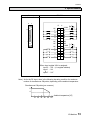
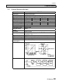
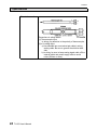
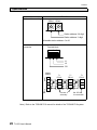
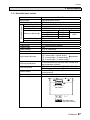
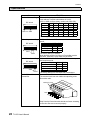
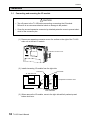
6F3B0255 UM-TS01∗∗∗-E034 PROGRAMMABLE CONTROLLER PROSEC USER’S MANUAL − I/O Modules − TOSHIBA CORPORATION T1-16S Important Information Misuse of this equipment can result in property damage or human injury. Because controlled system applications vary widely, you should satisfy yourself as to the acceptability of this equipment for your intended purpose. In no event will Toshiba Corporation be responsible or liable for either indirect or consequential damage or injury that may result from the use of this equipment. No patent liability is assumed by Toshiba Corporation with respect to use of information, illustrations, circuits, equipment or examples of application in this publication. Toshiba Corporation reserves the right to make changes and improvements to this publication and/or related products at any time without notice. No obligation shall be incurred other than as noted in this publication. This publication is copyrighted and contains proprietary material. No part of this book may be reproduced, stored in a retrieval system, or transmitted, in any form or by any means electrical, mechanical, photocopying, recording, or otherwise without obtaining prior written permission from Toshiba Corporation. © TOSHIBA Corporation 2001. All rights reserved DeviceNet is a trademark of the Open DeviceNet Vender Association, Inc. Publication number: UM-TS01∗∗∗-E034 1st edition December 2001, 2nd edition May 2002 6F3B0255 Safety Precautions This manual is prepared for users of Toshiba’s Programmable Controller T1-16S. Read this manual thoroughly before using the T1-16S. Also, keep this manual and related manuals so that you can read them anytime while the T1-16S is in operation. Hazard Classifications In the manuals related to the T1-16S, the following two hazard classifications are used to explain the safety precautions. ! WARNING Indicates a potentially hazardous situation which, if not avoided, could result in death or serious injury. ! CAUTION Indicates a potentially hazardous situation which, if not avoided, may result in minor or moderate injury. It may also be used to alert against unsafe practices. Even a precaution is classified as CAUTION, it may cause serious results depending on the situation. Observe all the safety precautions described on this manual. Safety Precautions ! CAUTION • Turn off power to the T1-16S before removing or mounting the option card or I/O module. Failure to do so can cause electrical shock or damage to the product. • Read the Safety Precautions described in the “T1-16S User’s Manual − Basic Hardware and Function −” before using the option cards and the I/O modules. • Follow the instructions described in this manual and in the “T1-16S User’s Manual − Basic Hardware and Function −” when installing and wiring the option cards or I/O modules. • The I/O modules have been designed for the T1-16S. Use your I/O modules only with the T1-16S. • Do not touch electronic components on the printed circuit board. It may cause damage to the product. I/O Modules 1 6F3B0255 About This Manual About This Manual This manual explains the specifications and operations of the I/O modules which are used with the T1-16S. The TOSLINE-F10 data link module is also covered in this manual. For your better understanding of the T1-16S, read the following manual at first to understand the T1-16S system, then read this manual. T1-16S User’s manual − Basic Hardware and Function − UM-TS01∗∗∗-E031 Terminology The following is a list of abbreviations and acronyms used in this manual. µs ASCII AWG CPU CRC EEPROM H I/O LED ms RAM ROM Vac Vdc 2 microsecond American Standard Code For Information Interchange American Wire Gage Central Processing Unit Cyclic Redundancy Checking Electrically Erasable Programmable Read Only Memory hexadecimal (when it appears in front of an alphanumeric string) Input/Output Light Emitting Diode millisecond Random Access Memory Read Only Memory AC voltage DC voltage T1-16S User’s Manual 6F3B0255 Contents Contents Safety Precautions 1 About This Manual 2 1. 1.1 1.2 1.3 1.4 System Configuration 5 T1-16S system configuration .....................................................................6 Using the I/O module .................................................................................7 Power capacity consideration ....................................................................8 Optional items ............................................................................................9 2. 2.1 2.2 2.3 2.4 2.5 2.6 2.7 2.8 2.9 2.10 2.11 2.12 Specifications 11 16 points DC input ...................................................................................12 16 points DC output .................................................................................14 8 points DC input and 8 points DC output combined ...............................16 8 points relay output ................................................................................18 1 channel analog input (0-5V/0-20mA) ....................................................19 1 channel analog input (±10V) .................................................................20 1 channel analog output (0-20mA) ..........................................................21 1 channel analog output (±10V) ..............................................................22 1 channel thermocouple input .................................................................23 TOSLINE-F10 remote station ..................................................................25 DeviceNet slave module ..........................................................................27 How to display the I/O status on the LED ................................................29 3. 3.1 Installation 31 Connecting and removing the I/O module ................................................32 4. 4.1 4.2 4.3 4.4 4.5 I/O Allocation 33 I/O allocation overview .............................................................................34 I/O allocation method ...............................................................................36 Register assignment rule .........................................................................37 Option (OPT) module ...............................................................................37 I/O allocation examples ..........................................................................39 5. 5.1 5.2 5.3 About the TOSLINE-F10 43 Network configuration ..............................................................................44 Register assignment ................................................................................45 RAS information ......................................................................................46 6. 6.1 6.2 6.3 6.4 6.5 About the DeviceNet slave 47 DeviceNet conformity ...............................................................................48 LED indication .........................................................................................48 Data allocation for DN111M .....................................................................49 Conformity for CE marking of DN111M ...................................................50 DeviceNet Wizard for TOSHIBA ..............................................................50 I/O Modules 3 6F3B0255 4 T1-16S User’s Manual 6F3B0255 Section 1 System Configuration 1.1 1.2 1.3 1.4 T1-16S system configuration, 6 Using the I/O module, 7 Power capacity consideration, 8 Optional items, 9 I/O Modules 5 6F3B0255 1. System Configuration 1.1 T1-16S system configuration The following figure shows the T1-16S system configuration. MMI/SCADA system Peripheral tool IBM-PC compatible personal computer Inverter IBM-PC compatible personal computer RS-485 (Enhanced version only) T-PDS software T1-16S main unit I/O modules T1-16S Handy programmer HP911A RS232C 8 modules max. Computer link function MMI/SCADA system 6 T1-16S User’s Manual Scope of this manual 6F3B0255 1. System Configuration 1.2 Using the I/O module The T1-16S has an expansion connector for connecting the I/O module on the right side of the unit. Maximum eight I/O modules can be connected to the T1-16S main unit. If eight 16-point modules are connected, the T1-16S can control 144 I/O points. The following 10 types of the I/O modules are available. Type DI116M DO116M DD116M RO108M AD121M AD131M DA121M DA131M TC111M FR112M DN111M Description 16 points input, 24 Vdc - 5 mA 16 points output, 24 Vdc - 100 mA 8 points input, 24 Vdc - 5 mA + 8 points output, 24 Vdc - 100 mA 8 points relay output, 24Vdc/240Vac - 1A 1 channel analog input 0-5V/0-20mA 1 channel analog input ±10V 1 channel analog output 0-20mA 1 channel analog output ±10V 1 channel thermocouple input TOSLINE-F10 remote station, 1 word input + 1 word output DeviceNet slave module, 4 word input + 4 word output, 8 word input + 8 word output, 12 word input + 12 word output, 16 word input + 16 word output (selectable) Power supply Supplied from the basic unit (5 Vdc). See section 1.3. • Up to eight I/O modules can be connected. • The TOSLINE-F10 card (FR112M) can be used together with other I/O modules. However only one FR112M is allowed at a time. The FR112M must be connected at the right end. • When the DeviceNet slave (DN111M) is used, the T1-16S must be version 1.1 or after. • The DeviceNet slave (DN111M) can be used together with other I/O modules. However only one DN111M is allowed at a time. • Cable side connector for the discrete I/O card (DI116M, DO116M or DD116M) is not supplied with the I/O module. This connector is separately available. See section 1.4. • Some I/O modules require jumper plug settings on the board. For this purpose, a screw (puller) for removing the internal board from the module case is attached to the I/O module. Expansion connector I/O module T1-16S main unit Max. 8 modules I/O Modules 7 6F3B0255 1. System Configuration 1.3 Power capacity consideration The maximum output current of the 5Vdc for I/O modules is decreased if 24Vdc service power is used. See the figure on the right. Also, the 5Vdc power is consumed by the handy programmer HP911A and the T1-16S's RS-485 communication port, if they are used. See below. • The HP911A consumes 0.2A. • The RS-485 port consumes 0.1A. 5Vdc maximum load current The T1-16S main unit supplies internal 5Vdc for I/O modules. The 5Vdc output capacity of the T1-16S main unit is as follows. (A) 1.5 1.0 0.1 0.2 (A) 24Vdc service power For example, if you do not use the 24Vdc service power, HP911A, and RS-485 port, the T1-16S can supply 1.5A = 1500mA of 5Vdc for I/O modules. And if you use 0.2A of 24Vdc service power and the RS-485 port, the maximum 5Vdc current for I/O modules is 1.0 - 0.1 = 0.9A = 900mA. The table below shows the maximum current consumption of 5 Vdc power of each I/O module. When using the I/O modules, confirm that the total current consumption is within the T1-16S’s output capacity. I/O module DI116M DO116M DD116M RO108M AD121M AD131M DA121M DA131M TC111M FR112M DN111M 8 16 points DC input 16 points DC output Combination 8 inputs and 8 outputs 8 points relay outputs 1 channel analog input 0-5V/0-20mA 1 channel analog input ±10V 1 channel analog output 0-20mA 1 channel analog output ±10V 1 channel thermo-couple input TOSLINE-F10 remote station DeviceNet slave module T1-16S User’s Manual 5Vdc current consumption (max.) 50mA 50mA 50mA 260mA 260mA 260mA 350mA 240mA 400mA 100 mA 250mA 6F3B0255 1. System Configuration 1.4 Optional items The following optional items related to the I/O modules are available. Item I/O connector Type PT15S PT15F Description Cable side connector for Soldering type DI116M, DO116M, or DD116M Flat cable type Note) The I/O connector (cable side connector) for the discrete I/O module (DI116M, DO116M or DD116M) is also available on the market. Refer to the followings. Connector maker: Fujitsu (1) Card side (PWB side) connector Type: FCN-365P024-AU (2) Cable side connector [soldering type] Type: FCN-361J024-AU (connector) Type: FCN-360C024-E (cover) (3) Cable side connector [flat cable type] Type: FCN-367J024-AU/F Use above (2) or (3). I/O Modules 9 6F3B0255 10 T1-16S User’s Manual 6F3B0255 Section 2 Specifications 2 2.1 16 points DC input, 12 2.2 16 points DC output, 14 2.3 8 points DC input and 8 points DC output combined, 16 2.4 8 points relay output, 18 2.5 1 channel analog input (0-5V/0-20mA), 19 2.6 1 channel analog input (±10V), 20 2.7 1 channel analog output (0-20mA), 21 2.8 1 channel analog output ( ±10V), 22 2.9 1 channel thermocouple input, 23 2.10 TOSLINE-F10 remote station, 25 2.11 DeviceNet slave module, 27 2.12 How to display the I/O status on the LED, 29 I/O Modules 11 6F3B0255 2. Specifications 2.1 16 points DC input Item Card type I/O allocation type Number of input points Rated input voltage Rated input current Minimum ON voltage Maximum OFF voltage ON delay time OFF delay time De-rating condition Input signal display External connection Withstand voltage Current consumption Internal circuit DI116M DC input, current sourcing/sinking X 1W (1 input register XW assigned) 16 points (8 points/common) 24 Vdc, +10/-15 % 5 mA (at 24 Vdc) 18.0 Vdc 6.0 Vdc 10 ms 10 ms See Note on the next page None (It can be displayed on the T1-16S main unit. Refer to section 2.11) 24-pin connector 1500 Vac, 1 minute (internal ↔ external circuits) Max. 50 mA (5 Vdc) 0 1 7 COM0 8 F COM1 12 T1-16S User’s Manual Internal circuit 6F3B0255 2. Specifications Item Terminal connection B DI116M A 12 1 + B A NC F 12 11 12 COM1 11 E D 10 10 B 9 9 9 8 8 8 NC 7 7 NC NC 6 6 NC 7 5 5 NC COM0 4 4 6 5 3 3 4 3 2 2 2 1 1 1 0 + C A + + When input register XW n is assigned; Input 0 ... Xn0 (n is register address) Input 1 ... Xn1 Input F ... XnF Note) As for the DC input, there is the following de-rating condition for maximum number of simultaneous ON points, depending on the ambient temperature. Simultaneous ON points (per common) 8 4 0 10 20 30 40 50 60 Ambient temperature [°C] I/O Modules 13 6F3B0255 2. Specifications 2.2 16 points DC output Item Card type I/O allocation type Number of output points Rated load voltage Maximum load current Voltage drop at ON Leakage current at OFF ON delay time OFF delay time Output signal display External connection Withstand voltage Current consumption Internal circuit DO116M Transistor output, current sinking Y 1W (1 output register YW assigned) 16 points (8 points/common) 5 to 24 Vdc, +10/-5 % 100 mA/point (at 24 Vdc), 20 mA/point (at 5 Vdc), 800 mA/common 0.4 V or less 100 µA 1 ms 2 ms None (It can be displayed on the T1-16S main unit. Refer to section 2.11) 24-pin connector 1500 Vac, 1 minute (internal ↔ external circuits) Max. 50 mA (5 Vdc) Vin0 0 Internal circuit 1 7 COM0 Vin1 8 F COM1 14 T1-16S User’s Manual 6F3B0255 2. Specifications Item Terminal connection B DO116M A + 12 1 + B A COM1 12 F 11 12 Vin1 11 E D 10 10 B 9 9 9 8 8 8 NC 7 7 NC NC COM0 6 6 5 5 NC Vin0 7 4 4 6 5 3 3 4 3 2 2 2 1 1 1 0 C A When output register YW n is assigned; Output 0 ... Yn0 (n is register address) Output 1 ... Yn1 Output F ... YnF I/O Modules 15 6F3B0255 2. Specifications 2.3 8 points DC input and 8 points DC output combined Item Card type Output Input I/O allocation type Number of input points Rated input voltage Rated input current Minimum ON voltage Maximum OFF voltage ON delay time OFF delay time De-rating condition Number of output points Rated load voltage Maximum load current Voltage drop at ON Leakage current at OFF ON delay time OFF delay time I/O signal display External connection Withstand voltage Current consumption Internal circuit DD116M DC input (current sinking/sourcing), Transistor output (current sinking), combined X+Y 2W (1 input XW and 1 output YW registers assigned) 8 points (8 points/common) 24 Vdc, +10/-15 % 5 mA (at 24 Vdc) 18.0 Vdc 6.0 Vdc 10 ms 10 ms See Note on the next page 8 points (8 points/common) 5 to 24 Vdc, +10/-5 % 100 mA/point (at 24 Vdc), 20 mA/point (at 5 Vdc), 800 mA/common 0.4 V or less 100 µA 1 ms 2 ms None (It can be displayed on the T1-16S main unit. Refer to section 2.11) 24-pin connector 1500 Vac, 1 minute (internal ↔ external circuits) Max. 50 mA (5 Vdc) 0 Internal circuit 1 DC input 7 COM0 Vin1 0 1 7 COM1 16 T1-16S User’s Manual DC output 6F3B0255 2. Specifications Item Terminal connection B DD116M A + B A COM1 12 7 11 12 Vin1 11 6 5 10 10 3 9 9 1 8 8 0 NC 7 7 NC NC 6 6 NC 7 5 5 NC COM0 4 4 6 5 3 3 4 3 2 2 2 1 1 1 0 12 1 4 2 + + When input register XW n and output register YW n+1 is assigned; Input 0 ..... Xn0 ( n is register address) Input 7 ...... Xn7 Output 0 ... Yn+10 (n+1 is next register address of n) Output 7 ... Yn+17 Note) As for the DC input, there is the following de-rating condition for maximum number of simultaneous ON points, depending on the ambient temperature. Simultaneous ON points (per common) 8 4 0 10 20 30 40 50 60 Ambient temperature [°C] I/O Modules 17 6F3B0255 2. Specifications 2.4 8 points relay output Item Card type I/O allocation type Number of output points Rated load voltage Maximum load current ON resistance Leakage current at off Minimum load ON/OFF delay time Output signal display Terminal block (removable) Screw size Screw torque Wire size Mechanical switching life Electrical switching life Insulation resistance Withstand voltage Current consumption Internal circuit RO108M Relay output Y 1W (1 output register YW assigned) 8 points (8 points/common) 240Vac/24Vdc 1A/point (resistive load), 4A/common 30mΩ or less (initial value) None 5Vdc, 10mA 10ms or less None (It can be displayed on the T1-16S main unit. Refer to section 2.11) M2 0.2 - 0.4Nm 0.3 - 1.25mm2 (AWG 22 - 16) 20 million times or more 100 thousand times or more (at max. rated voltage and current) internal circuit) 1500Vac, 1 minute (between terminal block and internal circuit) Max. 260mA (5Vdc) RY Internal circuit 0 RY 7 C 18 T1-16S User’s Manual 6F3B0255 2. Specifications 2.5 1 channel analog input (0-5V/0-20mA) Item Card type I/O allocation type Number of input points Resolution Rated input range Absolute max. input Rated input impedance Overall accuracy Conversion cycle External power supply Insulation Input signal display External connection Withstand voltage Current consumption Input range setting (jumper plug JP1) Data format AD121M Analog input X 1W (1 input XW register assigned) 1 channel 12 bits (1/4000) 0-5V 0 - 20 mA ±7 V ±25 mA 1 MΩ or more 250 Ω ±0.5 % FS : 25°C ±1 % FS : 0 to 55°C 2ms None Photo-coupler None (It can be displayed on the T1-16S main unit. Refer to section 2.11) 2-pin removable connector 500 Vac, 1 minute (internal ↔ external circuits) Max. 260 mA (5 Vdc) Open Short (factory setting) Converts full scale analog input signal (0-20mA/ 0-5V) into digital data in 0 to 4000. F XW E D C B A 9 8 7 6 5 4 3 2 1 0 0 0 0 0 D D D D D D D D D D D D D: Data bit (12bits) 0 - 4000 (H0000 - H0FA0) 0-20mA: D=200 × A 0-5V: D = 800 × A A: Analog value D: Digital value 4000 Digital value 2000 0 Internal circuit 10 2.5 P AMP N 250Ω Terminal connection 20 (mA) Analog value 5 (V) AD conversion unit Photocoupler Internal circuit Jumper plug Shielded two-core twisted pair cable + ↑ P 2 N 1 V − Grounding I/O Modules 19 6F3B0255 2. Specifications 2.6 1 channel analog input (±10V) Item Card type I/O allocation type Number of input points Resolution Rated input range Absolute max. input Rated input impedance Overall accuracy Conversion cycle External power supply Insulation Input signal display External connection Withstand voltage Current consumption Data format AD131M Analog input X 1W (1 input XW register assigned) 1 channel 12 bits (1/4000) ±10 V ±13 V 1 MΩ or more ±0.5 % FS : 25°C ±1 % FS : 0 to 55°C 2ms None Photo-coupler None (It can be displayed on the T1-16S main unit. Refer to section 2.11) 2-pin removable connector 500 Vac, 1 minute (internal ↔ external circuits) Max. 260 mA (5 Vdc) Converts full scale analog input signal (±10V) into digital data in -2000 to +2000. F XW E D C B A 9 8 7 6 5 4 3 2 1 0 S S S S S D D D D D D D D D D D S: Sign 0 = positive, 1 = negative D: Data bit (11bits) -2000 - 2000 (HF830 - H07D0) Negative value is expressed by 2’s complement D = 200 × A Digital value 2000 A: Analog value D: Digital value 1000 -10 -5 0 5 -1000 10 Analog value (V) -2000 Internal circuit P AM P N AD conversion unit Photocoupler Internal circuit AG Terminal connection Shielded two-core twisted pair cable + P 2 N 1 V − Grounding 20 T1-16S User’s Manual 6F3B0255 2. Specifications 2.7 1 channel analog output (0-20mA) Item Card type I/O allocation type Number of input points Resolution Rated input range Rated input impedance Overall accuracy Conversion cycle External power supply Insulation Output signal display External connection Withstand voltage Current consumption Data format DA121M Analog output Y 1W (1 output YW register assigned) 1 points 12 bits (1/4000) 0 - 20 mA 600 Ω or less ±0.5 % FS : 25°C ±1 % FS : 0 to 55°C 2ms None Photo-coupler None (It can be displayed on the T1-16S main unit. Refer to section 2.11) 2-pin removable connector 500 Vac, 1 minute (internal ↔ external circuits) Max. 350 mA (5 Vdc) Converts digital data in 0 to 4000 into analog signal in full scale (0-20mA) F YW E D C B A 9 8 7 6 5 4 3 2 1 0 ∗ ∗ ∗ ∗ D D D D D D D D D D D D D: Data bit (12bits) 0 - 4000 (H0000 - H0FA0) ∗: No effect on D/A conversion A= 0.005 × D A: Analog value D: Digital value 20 Analog value (mA) 15 10 5 0 2000 4000 Digital value Internal circuit Internal circuit Photocoupler P DA conversion unit AM P BUF N AG Terminal connection Shielded two-core twisted pair cable 2 P 1 N + Load − Grounding I/O Modules 21 6F3B0255 2. Specifications 2.8 1 channel analog output (±10V) Item Card type I/O allocation type Number of output points Resolution Rated output range Rated output impedance Overall accuracy Conversion cycle External power supply Insulation Output signal display External connection Withstand voltage Current consumption Data format DA131M Analog output Y 1W (1 output YW register assigned) 1 channel 12 bits (1/4000) ± 10V 10k Ω or more ±0.5 % FS : 25°C ±1 % FS : 0 to 55°C 2ms None Photo-couple None (It can be displayed on the T1-16S main unit. Refer to section 2.11) 2-pin removable connector 500 Vac, 1 minute (internal ↔ external circuits) Max. 240 mA (5Vdc) Converts digital data in -2000 to +2000 into analog signal in full scale (±10V) F E D C B A 9 8 7 6 5 4 3 2 1 0 YW S S S S S D D D D D D D D D D D S: Sign 0 = positive, 1 = negative D: Data bit (11bits) -2000 - 2000 (HF830 - H07D0) Negative value is expressed by 2’s complement A = 0.005 x D A: Analog value D: Digital value Analog value (V) 10 5 -2000 -1000 0 1000 2000 -5 Digital value -10 Internal circuit Internal circuit Photocoupler P DA conversion unit AM P BUF AG Terminal connection Shielded two-core twisted pair cable 2 P 1 N + Load − Grounding 22 T1-16S User’s Manual N 6F3B0255 2. Specifications 2.9 1 channel thermocouple input Item Card type I/O allocation type Input points Type of input (*1) Rated input range Load impedance Resolution Input range for T1 Overall accuracy Conversion cycle External power supply Insulation Input signal display External connection Withstand voltage External connection Current consumption Data format TC111M Thermocouple input X 1W (1 input XW register assigned) 1 channel Type K Type J Type E -200 to 1200ºC -200 to 800ºC -200 to 600ºC mV input -50 to +50mV 1MΩ or more 0.63ºC 0.4ºC 0.3ºC 25µV -2000 to 12000 -2000 to 8000 -2000 to 6000 -2000 to +2000 ±1%FS ±1ºC 20ms or less None Photo-coupler None (It can be displayed on the T1-16S main unit. Refer to section 2.11) 2-pin removable connector 500 Vac, 1 minute (internal ↔ external circuits) 2-pin removable terminal block Max. 400mA (5Vdc) Internal circuit I/O Modules 23 6F3B0255 2. Specifications Terminal connection Precautions in wiring cables. (1) Thermocouple input In wiring, pay attention to the polarity of thermocouple. (2) mV voltage input a) Use shielded two-core twisted pair cable in wiring analog cable. Be sure to ground the shield at load side. b) In wiring, be sure to keep analog signal cable off the external cable and power supply cable to avoid noise (200mm or more). 24 T1-16S User’s Manual 6F3B0255 2. Specifications 2.10 TOSLINE-F10 remote station FR112M function TOSLINE-F10 system Item Card type I/O allocation type Transmission cable Configuration Transmission speed Transmission distance Transmission data capacity (cyclic scan) Scan cycle Error checking Register assignment Transmission speed Transmission line termination Receive data at transmission error Status display External connection Current consumption Jumper settings FR112M TOSLINE-F10 remote station TL-F (no I/O register assigned) Shielded twisted-pair cable Bus (party line) 750 kbps or 250 kbps Max. 500 m (750 kbps) Max. 1 km (250 kbps) Max. 32 words (512 points) 7 ms/32 words (750 kbps) 12 ms/32 words (250 kbps) CRC check SW34 ... Data send to the master SW35 ... Data receive from the master (2 words of transmission data shared) 750 kbps or 250 kbps, Jumper selection (JPS) Jumper selection (JPR) Previous data is held (TOSLINE-F10 error flag S00D comes ON) None (It can be displayed on the T1-16S main unit. Refer to section 2.11) 3-pin removable terminal block Max. 100 mA (5 Vdc) JPS Internal bus connector JPR Terminal block 1 2 3 Rotary switch RSW1 Rotary switch RSW0 JPS: Transmission speed Open ... 750 kbps Short ... 250 kbps JPR: Termination resistor Open ... No connect Short ... Connect I/O Modules 25 6F3B0255 2. Specifications Item Station address setting FR112M RSW0 RSW1 0 0 Station address 10’s digit Station address 1’s digit Allowable station address: 0 to 30 Transmission cable connection Terminal block 1 2 3 L1 L2 SG Master station TERM T1 FR112 T1 FR112 T1 FR112 L1 L1 L1 L1 L2 L2 L2 L2 SG SG SG SG FG Connect externally Set JPR ON for termination Note) Refer to the TOSLINE-F10 manual for details of the TOSLINE-F10 system. 26 T1-16S User’s Manual 6F3B0255 2. Specifications 2.11 DeviceNet slave module DeviceNet system Item Module type I/O allocation type Conformity specification Network configuration Network speed Maximum cable length Connectable cable Network terminal block Vendor ID Product type Product code Node address Function on DeviceNet Input/output data size Data synchronization RAS information Status display Current consumption Switch settings DN111M DeviceNet slave module OPT (no I/O register assigned) DeviceNet Rev 2.0 Bus structure (trunk line – branch line) 125/250/500kbps (selectable) Network speed Thick cable Thin cable 125kbps 500m 250kbps 250m 100m 500kbps 100m Thick cable or thin cable of DeviceNet specification 5-pin removable terminal block 71 (TOSHIBA) 12 (Communication adapter) 100 0 to 63 (selectable) Polling type slave device (1) 4 words input / 4 words output (2) 8 words input / 8 words output selectable (3) 12 words input / 12 words output (4) 16 words input / 16 words output Every 4 words (If the master device has more than 4 words data synchronization function) DN111M status information (DN111M to T1-16S) DN111M request command (T1-16S to DN111M) Bi-color LED (green and red) for module and network status Max. 250mA (5Vdc) / Max. 90mA (Network) SW1 SW10 DIP switch DeviceNet cable connection terminal I/O Modules 27 6F3B0255 2. Specifications Item Node address setting DIP switch ON SW1 SW6 DN111M SW1 to SW6 (6-bit) of the DIP switch is used to set the node address. Possible node address is 0 to 63. (SW1 to SW6 configure binary number with SW1 LSB) Address SW1 SW2 SW3 SW4 SW5 SW6 0 OFF OFF OFF OFF OFF OFF 1 ON OFF OFF OFF OFF OFF 2 OFF ON OFF OFF OFF OFF : 62 OFF ON ON ON ON ON 63 ON ON ON ON ON ON The factory setting is address 0. Network speed setting DIP switch ON SW7 SW8 In/out data size setting DIP switch ON SW9 SW10 DeviceNet cable connection SW7 and SW8 of the DIP switch is used to set the network speed. Speed SW7 SW8 125kbps OFF OFF 250kbps ON OFF 500kbps OFF ON N/A ON ON The factory setting is 125kbps. Note) Network speed of all nodes on DeviceNet must be the same. Otherwise, some nodes may be busoff. SW9 and SW10 of the DIP switch is used to set the input and output data size. Input + Output SW9 SW10 4 word + 4 word OFF OFF 8 word + 8 word ON OFF 12 word + 12 word OFF ON 16 word + 16 word ON ON The factory setting is 4 word input and 4 word output. Connect DeviceNet cable to a terminal block of DN111M. The terminal block has color labels corresponding to the DeviceNet cable. black blue “FG” white red cable fixing screw black blue drain white red Strip 5mm the DeviceNet cable sheath and insert according to the color. Be sure to connect properly. 28 T1-16S User’s Manual 6F3B0255 2. Specifications 2.12 How to display the I/O status on the LED On the T1-16S main unit, 16 points of I/O status LEDs are provided. L 0 1 2 3 4 5 6 7 H In the normal condition (default state), these LEDs indicate the main unit I/O status. However, these LEDs can also be used for displaying the I/O status of the connected I/O modules. The LED display contents are controlled by the value of the special register SW54. See table below. I/O status LEDs: Indicates the ON/OFF status of each I/O signal. SW54 value Display contents 0 (default) Main unit (L: X000-007, H: Y020-027) 1 I/O module slot 0 2 I/O module slot 1 3 I/O module slot 2 4 I/O module slot 3 5 I/O module slot 4 6 I/O module slot 5 7 I/O module slot 6 8 I/O module slot 7 9 TOSLINE-F10 (FR112M), Low 1 word 10 TOSLINE-F10 (FR112M), High 1 word Others Main unit (L: X000-007, H: Y020-027) Note It indicates I/O module status. (Effective only in RUN mode) By writing the following program in the T1-16S, the analog setting adjuster (V0) on the T1-16S main unit can be used to select the LED display contents. That is, you can display the I/O module ON/OFF status on the LED by adjusting the V0 using screwdriver. SW30 < 100 ... Main unit 100 ≤ SW30 < 200 ... Slot 0 I/O 200 ≤ SW30 < 300 ... Slot 1 I/O 300 ≤ SW30 < 400 ... Slot 2 I/O 400 ≤ SW30 < 500 ... Slot 3 I/O 500 ≤ SW30 < 600 ... Slot 4 I/O 600 ≤ SW30 < 700 ... Slot 5 I/O 700 ≤ SW30 < 800 ... Slot 6 I/O 800 ≤ SW30 < 900 ... Slot 7 I/O Note) Do not designate SW54 as the division result register directly. Otherwise the next register SW55 data will be changed unexpectedly. I/O Modules 29 6F3B0255 30 T1-16S User’s Manual 6F3B0255 Section 3 Installation 3 3.1 Connecting and removing the I/O module, 32 I/O Modules 31 6F3B0255 3. Installation 3.1 Connecting and removing the I/O module ! CAUTION • Turn off power to the T1-16S before connecting or removing the I/O module. Failure to do so can cause electrical shock or damage to the product. • Cover the unused expansion connector by attached protective cover to prevent shortcircuit of the connector pins. (1) Remove an expansion connector cover of a surface on the right of the T1-16S main unit or the last I/O module. Expansion connector cover (2) Installs increasing I/O module from the right side. Lock lever I/O module T1-16S main unit Expansion connector cover Lock lever Max. 8 modules (3) When remove the I/O module, move to the right side while it pushes top and bottom lock lever. 32 T1-16S User’s Manual 6F3B0255 Section 4 I/O Allocation 4 4.1 4.2 4.3 4.4 4.5 I/O allocation overview, 34 I/O allocation methods, 36 Register assignment rule, 37 Option (OPT) module, 37 I/O allocation examples, 39 I/O Modules 33 6F3B0255 4. I/O Allocation 4.1 I/O allocation overview The I/O allocation is the operation to let the T1-16S to recognize the type and location of the I/O modules which are connected to the T1-16S. The T1-16S has the information called “I/O allocation table” in its memory. This “I/O allocation table” indicates what type of module is connected on which slot. The contents of the I/O allocation table is as follows. Unit 0 1 Slot PU 0 1 2 3 4 5 6 7 0 1 2 3 4 5 6 7 I/O type PU slot must be blank Slot 0 is for main unit (XW00, XW01, YW02 and YW03 are assigned internally) X+Y 4W Slots 1 to 7 of unit 0 are reserved. (They must be blank) Expansion I/O slots. Connected I/O modules are allocated here. The figure below shows the correspondence between I/O allocation “Slot” and hardware location. Main unit = Unit 0 - Slot 0 I/O modules = Unit 1 - Slot 0 to 7 0 1 2 3 4 5 6 7 Slot number T1-16S Note 1) When the TOSLINE-F10 remote station module (FR112M) is used, only one FR112M is allowed with the T1-16S. The FR112M must be connected as the last (right end) module. As for the I/O allocation of the FR112M, different from the other I/O modules, the FR112M is allocated on the slot 3 or slot 7 regardless of physical connecting location. Note 2) When the DeviceNet slave module (DN111M) is used, only one DN111M is allowed. There is no restriction of the mounting position. 34 T1-16S User’s Manual 6F3B0255 4. I/O Allocation The “I/O type” indicates the type of module and assigned number of I/O registers (XW/YW registers). “X” means input, “Y” means output, and “X+Y” means input and output mixture types. And, for example, “4W” means 4 words of XW/YW registers are assigned. The table below shows the “I/O type” of each module. Basic unit / I/O module T1-16S main unit 16 points DC input 16 points DC output 8 points input + 8 points output 8 points relay output 1 channel analog input (12-bit) 1 channel analog output (12-bit) 1 channel thermocouple input TOSLINE-F10 remote station Note 1) DeviceNet slave module Note 2) DI116M DO116M DD116M RO108M AD121M AD131M DA121M DA131M TC111M FR112M DN111M I/O type X+Y 4W X 1W Y 1W X+Y 2W Y 1W X 1W X 1W Y 1W Y 1W X 1W TL-F OPT Note 1) The FR112M has the I/O type “TL-F”. No XW/YW register is assigned to the FR112M. For the FR112M, special registers SW34 and SW35 are assigned, instead of XW/YW registers. See section 5. Note 2) The DN111M has the I/O type “OPT”. No XW/YW register is assigned to the OPT module. For the OPT module, RW registers (from RW240 to RW255) and D registers (from D4000 to D4095) are assigned, instead of XW/YW registers. See section 6. I/O Modules 35 6F3B0255 4. I/O Allocation 4.2 I/O allocation method The operation to create the I/O allocation table is called “I/O allocation”. When the T1-16S is used without connecting I/O module, the I/O allocation is not required. Because the I/O allocation table for main unit is created automatically when the memory clear operation is performed. However, when I/O modules are used, or T1-16S’s user program is developed in offline, the I/O allocation is necessary. There are two methods for the I/O allocation. Automatic I/O allocation: When the automatic I/O allocation command is executed from the programmer, the T1-16S checks the hardware configuration, then creates the I/O allocation table. This method is useful when all the necessary hardware (I/O modules) is prepared. Manual I/O allocation: I/O type can be set onto the I/O allocation table slot by slot by the programmer. (Editing of the I/O allocation table) The table below shows the available I/O type by the manual I/O allocation. Function Number of I/O type registers assigned X 01, 02, 04, 08, or 16 Y 01, 02, 04, 08, or 16 X+Y 02, 04, 08, or 16 TL-F OPT - Description For input For output For input and output mixture For TOSLINE-F10 (no I/O register is assigned) For Option module such as DN111M (no I/O register is assigned) NOTE (1) Do not use the I/O type other than the listed above for the T1-16S. (2) To run the T1-16S, the I/O allocation table and physical I/O configuration must be matched. 36 T1-16S User’s Manual 6F3B0255 4. I/O Allocation 4.3 Register assignment rule Once the I/O allocation table is created, the T1-16S’s registers are assigned to the hardware (I/O module) according to the following rules. (1) Input register (XW) and output register (YW) have consecutive register addresses. That is, one address is for either XW or YW. (2) XW registers are assigned to the I/O type “X”. (3) YW registers are assigned to the I/O type “Y”. (4) XW and YW registers are assigned to the I/O type “X+Y”. Leading half are XW and following half are YW. (5) I/O registers (XW/YW) are assigned sequentially from slot 0. (6) T1-16S main unit has the I/O type “X+Y 4W”. Therefore, four registers (XW00, XW01, YW02 and YW03) are assigned to the main unit. XW01 and YW03 are assigned internally. (7) No register is assigned to a vacant slot. (8) For “TL-F”, special registers SW34 and SW35 are assigned. (9) For "OPT" module, RW registers (RW240 to RW255) and D registers (D4000 to D4095) are assigned, instead of XW/YW registers. See section 4.4. 4.4 Option (OPT) module The I/O module which has the special I/O type “OPT” are allocated to RW and D registers, instead of XW/YW registers. The module status and the request command are allocated to RW registers (RW240 to RW255), and the I/O data are allocated to D registers (D4000 to D4095). Note that the OPT setting is supported by the T1-16S version 1.1 or later. (1) Allocation of status data and request data Register RW240 RW241 RW242 RW243 RW244 RW245 RW246 RW247 RW248 RW249 RW250 RW251 RW252 RW253 RW254 RW255 1st OPT module 2nd OPT module 3rd OPT module 4th OPT module 5th OPT module 6th OPT module 7th OPT module 8th OPT module Contents Status data Request command Status data Request command Status data Request command Status data Request command Status data Request command Status data Request command Status data Request command Status data Request command I/O Modules 37 6F3B0255 4. I/O Allocation Note1) Contents of the status data and request command are due to each OPT module. Note2) The RW registers which are not assigned to OPT modules can be used for normal RW registers. For example, when one OPT module is connected, RW240 and RW241 are assigned to this OPT module. In this case, RW242 to RW255 can be used for normal RW registers. (2) Allocation of input/output data Input/output data of the OPT module are allocated to D4000 and after (up to D4095). The assigned data size is dependent on the OPT module. For example, if the 1st OPT module requires 8 words of I/O data, the 2nd OPT module requires 32 words of I/O data, and the 3rd OPT module requires 4 words of I/O data, the allocation is as follows. Register D4000 : D4007 D4008 : D4039 D4040 : D4043 D4044 : D4095 Contents 1st OPT module I/O data (8 words) 2nd OPT module I/O data (32 words) 3rd OPT module I/O data (4 words) Can be used for normal D register Note 1) The contents of the I/O data (in or out) are due to each OPT module. Note 2) The total I/O data of the connected OPT modules must be 96 words or less. If exceeded, the T1-16S comes error because of allocation error. Note 3) D registers which are not assigned to OPT modules can be used for normal D registers. 38 T1-16S User’s Manual 6F3B0255 4. I/O Allocation 4.5 I/O allocation examples Example 1 • Hardware configuration T1-16S FR112M (TL-F) DO116M (Y1W) DI116M (X1W) • I/O allocation table and register assignment Unit 0 1 Slot PU 0 0 1 2 3 I/O type X+Y 4W X 1W Y1W TL-F Assigned register XW00, YW02 XW04 YW05 SW34, SW35 Assigned device X000 - X007, Y020 - Y027 X040 - X04F Y050 - Y05F S340 - S34F, S350 - S35F • Hardware and register/device relation T1-16S X000-X007, Y020-Y027 SW34, SW35 Y050-Y05F X040-X04F Note 1) X008 to X01F, Y028 to Y03F are assigned internally. 2) As for the I/O allocation of FR112M, refer to the note on page 34. I/O Modules 39 6F3B0255 4. I/O Allocation Example 2 • Hardware configuration T1-16S RO108M (Y1W) TC111M (X1W) DA121M (Y1W) AD121M (X1W) • I/O allocation table and register assignment Unit 0 1 Slot PU 0 0 1 2 3 I/O type X+Y 4W X1W Y1W X1W Y1W Assigned register XW00, YW02 XW04 YW05 XW06 YW07 Assigned device X000 - X00F, Y020 - Y02F X040 - X04F Y050 - Y05F X060 - X06F Y070 - Y077 • Hardware and register/device relation T1-16S X000-X007, Y020-Y027 Y070-Y077 XW06 YW05 XW04 Note) X008 to X01F, Y028 to Y03F, Y078 to Y07F are assigned internally. 40 T1-16S User’s Manual 6F3B0255 4. I/O Allocation Example 3 • Hardware configuration T1-16S OPT (input 2W/output 6W) DN111M (input 4W/output 4W) DO116M (Y1W) DI116M (X1W) • I/O allocation table and register assignment Unit 0 1 Slot PU 0 0 1 2 I/O type Assigned register Assigned device X+Y 4W X1W Y1W OPT X000 - X00F, Y020 - Y02F X040 - X04F Y050 - Y05F None 3 OPT XW00, YW02 XW04 YW05 RW240: Status data RW241: Request command D4000-D4003: Input data D4004-D4007: Output data RW242: Status data RW243: Request command D4008-D4009: Input data D4010-D4015: Output data None • Hardware and register/device relation T1-16S X000-X007, Y020-Y027 RW242, RW243, D4008-D4015 X040-X04F RW240, RW241, D4000-D4007 Y050-Y05F Note 1) X008 to X01Fand Y028 to Y03F are assigned internally. Note 2) RW244 to RW255 can be used for normal RW registers. D4016 to D4095 can be used for normal D registers. I/O Modules 41 6F3B0255 42 T1-16S User’s Manual 6F3B0255 Section 5 About the TOSLINE-F10 5 5.1 Network configuration, 44 5.2 Register assignment, 45 5.3 RAS information, 46 I/O Modules 43 6F3B0255 5. About the TOSLINE-F10 5.1 Network configuration The FR112M is the TOSLINE-F10 remote station module for the T1-16S. By using the FR112M, high-speed data linkage between the T1-16S and the upper T-series PLC (T2/T2E/T2N or T3/T3H) becomes available. For details of the TOSLINE-F10 system, read separate TOSLINE-F10 user’s manual. The FR112M works as a remote station. One master station is necessary on a TOSLINE-F10 (hereafter called F10) network. The F10 master station has 32 words of scan transmission memory. The FR112M shares 2 words of them. (1 word transmit and 1 word receive) Therefore maximum 16 T1-16S’s can be connected to the master station. F10 master station (T2 station) T2E C P U M S 2 1 1 I/O F10 network Station 0 FR112M Station 2 FR112M Station 4 FR112M Station 30 FR112M T1-16S T1-16S T1-16S T1-16S (Max. 16 T1-16Ss) The FR112M shares 2 words of transmission memory. The shared addresses are determined by the station address of the FR112M. Master station transmission memory 0 1 2 3 4 5 Station 0 FR112 Station 2 FR112 Station 4 FR112 Station 30 FR112 30 31 44 T1-16S User’s Manual 6F3B0255 5. About the TOSLINE-F10 5.2 Register assignment In case of the T2 and T3 stations, the link registers LW are assigned to the TOSLINEF10 transmission memory. On the other hand, in case of the T1-16S, the special registers SW34 and SW35 are assigned fixedly. SW34 ... Transmit data to the master SW35 ... Receive data from the master The figure below shows an example of the data link map. < System configuration > F10 master station (T2 station) T2E C P U M S 2 1 1 I/O F10 network Station 0 FR112M Station 6 FR112M Station 10 FR112M T1-16S A T1-16S B T1-16S C < Data link map > F10 transmission address 0 1 T2E Master LW000 LW001 PLC reference T1-16S T1-16S A (#0) B (#6) SW34 SW35 6 7 LW006 LW007 SW34 SW35 10 11 LW010 LW011 T1-16S C (#10) Data source and destination T2E ← T1-16S A T2E → T1-16S A T2E ← T1-16S B T2E → T1-16S B SW34 SW35 T2E ← T1-16S C T2E → T1-16S C I/O Modules 45 6F3B0255 5. About the TOSLINE-F10 5.3 RAS information On the F10 network, its data linkage system is controlled by the master station. If the master station is failed, entire data linkage is stopped. In a normal data linkage situation, the transmission data validity is checked by receiver station using CRC. The table below shows the behavior of the T1-16S side in case of F10 related trouble. Trouble situation F10 operation Master station down Entire data linkage PLC CPU of master is stopped. station down Transmission cable broken Transmission error occurs frequently. Interference by noise, etc. Momentary transmission error occurs. FR112M hardware error Data link between the FR112M and master station is stopped. T1-16S behavior Special device S00D comes ON. Data in SW35 is not changed. T1-16S continues running. When an error is detected by the FR112M, special device S00D comes ON. S00D returns to OFF when data link is recovered. Data in SW35 is not changed during S00D is ON. T1-16S continues running. If the FR112M does not respond to the T1-16S, the T1-16S enters into Error mode. In the Error mode, all outputs of the T116S are switched OFF, and program execution is stopped. (PLC CPU of master station can know the error) NOTE The FR112M does not support the F10’s read-back check mode. Do not use the read-back check mode when T1-16S is linked. 46 T1-16S User’s Manual 6F3B0255 Section 6 About the DeviceNet slave 6 6.1 6.2 6.3 6.4 6.5 DeviceNet conformity, 48 LED indication, 48 Data allocation for DN111M, 49 Conformity for CE marking of DN111M, 50 DeviceNet Wizard for TOSHIBA, 50 I/O Modules 47 6F3B0255 6. About the DeviceNet slave 6.1 DeviceNet conformity The DN111M is a one of T1-16S option module, and acts as DeviceNet slave module. Via DN111M, the T1-16S can communicate with a master device (such as DN211A, DN311A, or DN611A) on DeviceNet. The DN111M has been tested by ODVA’s authorized Independent Test Lab and confirmed to comply with ODVA Conformance Test Software Version A-15. DeviceNet is a registered trademark of ODVA(Open DeviceNet Vendor Association). Note: The T1-16S version 1.1 or later is required for use of the DN111M. 6.2 LED indication The DN111M has a bi-color LED (green and red) that is called “MS/NS”. LED lighting represents DN111M status. LED Not lit Green blinking Green lighting Red blinking Red lighting Orange lighting 48 Module status 1) No power is supplied to the T1-16S. 2) T1-16S power is normal, but network power is not supplied. 3) T1-16S and network power are normal, but DN111M is alone on the DeviceNet network. DN111M is normal, but DN111M is not communicating with a master. DN111M is normal, and DN111M is communicating with a master. DN111M is encountering a recoverable trouble. (The master stops polling) 1) DN111M is down mode. 2) DN111M detects a duplicated node address. 3) DN111M detects busoff. Self check when the power is on. T1-16S User’s Manual 6F3B0255 6. About the DeviceNet slave 6.3 Data allocation of DN111M (1) Bit allocation of status data (Bit 3, 4, 5, 6, 7, 8, A and B are not used) Bit F E D C 9 2 1 0 Contents 1: DN111M is down. 0: DN111M is not down. 1: DN111M is initializing. 0: DN111M is not initializing. 1: DN111M is normal but cannot communicate, because of T1-16S is halt. 0: The other case. 1: DN111M is normal and can communicate (T1-16S is run). 0: The other case. 1: DN111M communicates with a master and DN111M receives valid data. 0: The other case. 1: DN111M detects busoff. Bit F is also “1” 0: DN111M does not detect busoff. 1: DN111M detects a duplicated node address. Bit F is also “1” 0: DN111M does not detect a duplicated node address. 1: DN111M has no network power. 0: DN111M has network power. (2) Bit allocation of request command (Bit 1 to bit F are not used) Bit 0 Contents 1: Reset request for DN111M. 0: Cancel the reset request. (3) Register allocation example DN111M (4 words input / 4 words output) is connected with the T1-16S. Status data RW240 Request command RW241 Input data area (received data from master) D4000 to D4003 Output data area (send data to master) D4004 to D4007 DN111M (16 words input / 16 words output) is connected with the T1-16S. Status data RW240 Request command RW241 Input data area (received data from master) D4000 to D4015 Output data area (send data to master D4016 to D4031 I/O Modules 49 6F3B0255 6. About the DeviceNet slave 6.4 Conformity for CE marking of DN111M DN111M can be conformed to the EMC directive and LVD directive (IEC61131-2) under the following condition. (1) EMC directive The transmission cable should be fitted with ferrite core. The ferrite cores must be clamped within 10cm from the DN111M. • Example of ferrite core impedance … 25MHz: 137Ω / 100MHz: 204Ω A shield line of the transmission cable must be connected to the ground that resistance must be 100 ohm or less. The transmission cable must be installed in protect pipes or steel ducts for whole cable. The pipes and ducts must have ground connection to the ground as short as possible, that resistance must be 100 ohm or less. (2) LVD directive Use reinforced insulation / double insulation DC power supply that provide to inputs/outputs, internal circuit and communication circuit. (3) Supplementary information It is necessary for you to confirm if your system is conform to the EC directive when applying our products, because system configuration (physical arrangement, wiring, other devices, connections to other equipment, etc.) may cause the EMC/LVD conditions to be changed. Please ask the qualified expert for installation of DeviceNet network because it requires sufficient safety and noise-suppression measures. 6.5 DeviceNet Wizard for TOSHIBA The EDS file of the DN111M is installed in the DeviceNet Wizard for TOSHIBA. The default setting of the input/output data size in the EDS file is “4 words input + 4 words output”, ie. 8 bytes input and 8 bytes output. If you want to use DN111M with other input/output setting, please change the setting as follows. 1) Using a network configuration screen on the DeviceNet Wizard, register DN111M onto a master. 2) Using a Scan List Editor on the DeviceNet Wizard, change the input/output setting of the DN111M. NOTE 50 If you use a configuration tool from other vendors, you can download the EDS file for the DN111M from ODVA Web site (http://www.odva.org). T1-16S User’s Manual 6F3B0255 6. About the DeviceNet slave For your information, the contents of the DN111M EDS file is shown below. [File] DescText = CreateDate CreateTime Revision = "DN111 EDS File"; = 01-28-2002; $ 2002/01/28 = 10:00:00; 1.0; $ Revision of EDS [Device] VendCode = 71; VendName = "TOSHIBA CORPORATION"; ProdType = 12; ProdTypeStr = "Communication Adapter"; ProdCode = 100; ProdName = "DN111 Slave Module"; MajRev = 1; MinRev = 1; Catalog = ""; [IO_Info] Default = 0x0001; PollInfo = 0X0001, 1, 1; $ Poll $ Poll $ Default input = 1 $ Default output = 1 Input1 = 8, $ 8byte 0, $ All bits are significant 0x0001, $ Poll Connection "Pararel Input", $ Name of this I/O 6, $ Path Length "20 07 24 02 30 04",$ Class7,Instance2,Attribute4 ""; Output1 = 8, $ 8byte 0, $ All bits are significant 0x0001, $ Poll Connection only "Pararel Output", $ Name of this I/O 6, $ Path Length "20 07 24 01 30 04",$ Class7,Instance1,Attribute4 ""; I/O Modules 51 TOSHIBA CORPORATION Industrial Equipment Department 1-1, Shibaura 1-chome, Minato-ku Tokyo 105-8001, JAPAN Tel: 03-3457-4900 Fax: 03-5444-9268