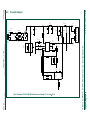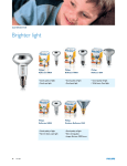
1
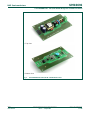
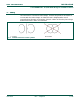
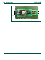
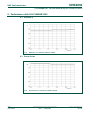
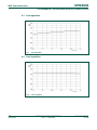
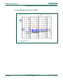
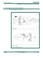
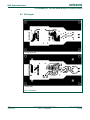
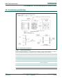
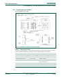
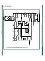
UM10692
SSL2109ADB1105 - 120 V/18 W PAR38 high PF isolated LED
driver demo board
Rev. 1 — 9 April 2013
User manual
Document information
Info
Content
Keywords
SSL2109ADB1105, flyback converter, high PF, PAR38
Abstract
This document describes the operation of a 120 V/18 W non-dimmable
LED driver demo board featuring SSL2109A and using an isolated
flyback topology. The SSL2109ADB1105 demo board is designed for
both PAR38 and PAR30 form factors used in Solid State Lighting (SSL)
applications
UM10692
NXP Semiconductors
SSL2109ADB1105 - 120 V/18 W PAR38 high PF isolated LED driver
Revision history
Rev
Date
Description
v.1
first issue
UM10692
User manual
20130409
All information provided in this document is subject to legal disclaimers.
Rev. 1 — 9 April 2013
© NXP B.V. 2013. All rights reserved.
2 of 28
UM10692
NXP Semiconductors
SSL2109ADB1105 - 120 V/18 W PAR38 high PF isolated LED driver
1. Introduction
This user manual describes the operation of the SSL2109ADB1105 demo board
featuring the SSL LED driver SSL2109A in a 120 V/18 W isolated application.
The SSL2109ADB1105 demo board is designed for driving a 10-LED string load.
The PCB dimensions are compatible with both PAR38 and PAR30 form factors used in
SSL applications.
The demo board provides a simple and effective solution having high power factor, low
THD and high efficiency for SSL applications.
1.1 Features of the application
• PAR38 and PAR30 form factor compatibility
• Open LED and short circuit LED string protection
• OverCurrent protection (OCP) and OverTemperature protection (OTP)
• Power factor (PF) greater than 0.9 and THD < 20 %
• Efficiency greater than 85 %
• Minimal changes required in design for a 230 V/18 W SSL application
• Compliant with IEC61000-3-2 harmonics standard
• Compliant with FCC15 EMC standard
The assembled top and bottom board views are shown in Fig 1 with the board
dimensions in Fig 3. The board dimensions allow enough headroom with either PAR38 or
PAR30 lamps.
UM10692
User manual
All information provided in this document is subject to legal disclaimers.
Rev. 1 — 9 April 2013
© NXP B.V. 2013. All rights reserved.
3 of 28
UM10692
NXP Semiconductors
SSL2109ADB1105 - 120 V/18 W PAR38 high PF isolated LED driver
a. Top view
b. Bottom view
Fig 1.
UM10692
User manual
SSL2109ADB1105 120 V/18 W PAR38 demo board
All information provided in this document is subject to legal disclaimers.
Rev. 1 — 9 April 2013
© NXP B.V. 2013. All rights reserved.
4 of 28
UM10692
NXP Semiconductors
SSL2109ADB1105 - 120 V/18 W PAR38 high PF isolated LED driver
2. Safety
The board must be connected to mains voltage. Avoid touching the demo board while it
is connected to the mains voltage. An isolated housing is obligatory when used in
uncontrolled, non-laboratory environments. Galvanic isolation of the mains phase using a
variable transformer is always recommended.
a. Isolated
Fig 2.
b. Not isolated
Variable transformer isolation symbols
UM10692
User manual
All information provided in this document is subject to legal disclaimers.
Rev. 1 — 9 April 2013
© NXP B.V. 2013. All rights reserved.
5 of 28
UM10692
NXP Semiconductors
SSL2109ADB1105 - 120 V/18 W PAR38 high PF isolated LED driver
3. Specifications
Table 1.
Symbol
Specifications of the SSL2109ADB1105
Parameter
Value
V mains
AC mains supply voltage
120 V; ±10 %
P in
input power
17.6 W at nominal V mains = 120 V
P out
output power
15.4 W
V LED
output voltage (LED voltage) 25 V to 40 V with nominal V LED = 35 V
I LED
output current (LED current) 455 mA
I ripple
output ripple current
∆I LED / ∆V mains
line regulation
130 mA (p-p)
1.9 mA/V
(±5 % I LED at ±10 % V mains variation)
∆I LED / ∆V LED
load regulation
η
efficiency
88 %
PF
power factor
0.98
THD
total harmonic distortion
15 %
f sw
switching frequency
70 kHz
2 mA/V
(±1.65 % I LED at ±10 % V LED variation)
UM10692
User manual
All information provided in this document is subject to legal disclaimers.
Rev. 1 — 9 April 2013
© NXP B.V. 2013. All rights reserved.
6 of 28
UM10692
NXP Semiconductors
SSL2109ADB1105 - 120 V/18 W PAR38 high PF isolated LED driver
Fig 3.
UM10692
User manual
SSL2109ADB1105 demo board dimensions
All information provided in this document is subject to legal disclaimers.
Rev. 1 — 9 April 2013
© NXP B.V. 2013. All rights reserved.
7 of 28
UM10692
NXP Semiconductors
SSL2109ADB1105 - 120 V/18 W PAR38 high PF isolated LED driver
4. Functional description
4.1 Input filtering
Common-mode and differential mode π filters are implemented to reduce common-mode
or differential mode noise originating from the high-frequency (HF) switching
currents/voltages in the primary of the converter from returning to the mains. This noise
must be kept to a minimum by:
• Small primary current loop (C2 to pin 1 of T1, pin 3 of T1 to drain of external
MOSFET Q5, ground return from sense resistors R1, R24, R26 to C2 ground)
• Snubber components D3, R17, C8 closely parallel to pins 1 and 3 of T1
• Track length from pin 3 of T1 to drain of external MOSFET to be small in order to
reduce capacitance to surroundings
For this 18 W application, C2 must be chosen sufficiently large to act as a buffer for the
HF current flowing in the primary but also small enough to maintain a high PF where a
value of 330 nF for C2 is a good compromise.
4.2 PF adjustment
The divider network consisting of R5, R6, R7, R9, R10, D4, C10 and C11 modulates the
base of Q7 according to the rectified mains. Consequently, a modulating current set by
R11 flows through R8 and the sense current through R1, R24 and R26 is also
modulated. Depending on the divider resistor values, the HF current through the primary
has a current with a rectified mains modulation resulting in a high PF.
The PF can be increased/decreased by decreasing/increasing R5 and R6 and a
compromise can be reached between PF and line regulation.
4.3 RCD clamp
Leakage inductance of the transformer is in series with primary inductance and the drain
of MOSFET Q5. This leakage inductance together with the parasitic capacitance across
the drain source of Q5 causes HF ringing when Q5 switches off. If the leakage is not
minimized the voltage at the drain reaches high voltages levels which can damage Q5 if
voltage levels exceed the maximum allowable level.
An RCD clamp (R17, C8 and D3) prevents the voltage on the drain of Q5 exceeding the
maximum drain voltage when Q5 switches off.
4.4 Supply voltage
The supply voltage of the SSL2109A is achieved using an auxiliary winding. As further
advantages, the auxiliary winding provides, via a resistor R25 on its underwinding, both a
simple solution for improved load regulation using R12 and open-circuit protection (OCP)
via the NTC pin using R13.
4.4.1 Open circuit protection
If no LED string is connected to the converter output, the voltage can quickly exceed the
maximum rating of the output capacitors C3 and C7.
The underwinding of the auxiliary is connected to resistor R25 to prevent this. The
voltage across R25 decreases as the output voltage increases. Consequently, the
voltage at the NTC pin decreases once the current through R13 exceeds the internal
current of the NTC pin. When the NTC voltage drops below 0.35 V then the SSL2109A
UM10692
User manual
All information provided in this document is subject to legal disclaimers.
Rev. 1 — 9 April 2013
© NXP B.V. 2013. All rights reserved.
8 of 28
UM10692
NXP Semiconductors
SSL2109ADB1105 - 120 V/18 W PAR38 high PF isolated LED driver
switches off.
An external 18 V Zener diode is included at the VCC pin to prevent that the voltage
exceeds 20 V at the VCC pin for this no LED string situation
4.4.2 Short circuit
When the LED terminals are shorted, the SSL2109A defaults to its maximum
demagnetization time of 36 µs. This prevents that the transformer current ramps up to an
excessively large value while the input power is limited and the SSL2109A enters OPS
protection (latched) mode.
Remark:
Do not try to short-circuit the LED output while the circuit is powered or without
discharging C3. The short-circuit protection is intended for zero-hour short circuit
protection (so a short circuit during first assembly before power is applied).
UM10692
User manual
All information provided in this document is subject to legal disclaimers.
Rev. 1 — 9 April 2013
© NXP B.V. 2013. All rights reserved.
9 of 28
UM10692
NXP Semiconductors
SSL2109ADB1105 - 120 V/18 W PAR38 high PF isolated LED driver
5. Demo board connections
The SSL2109ADB1105 demo board is supplied with a 120 V, 60 Hz mains supply where
the board connection is shown in Fig 4.
Table 2.
Input and output connections
Connector
Function
Remark
L
AC MainsL
line wire solder connection on
small board
N
AC MainsN
neutral wire solder connection
on small board
+
LED anode
positive LED wire solder
connection on small board
-
LED cathode
negative LED wire solder
connection on small board
X5
AC mains input
AC mains in terminal block
X6
LED load output
LED connector 6-way female
for NXP LED load
Remarks:
Make all connections with the input mains supply switched off.
Use a protective shield over application and never touch the board when measuring or
testing.
Connections and testing:
• Connect a 10-LED string load to the SSL2109ADB1105 together with power meters
at both inputs and outputs.
• Connect V mains (120 V (AC)/60 Hz) using an isolating transformer (initially set to 0 V)
to the input connection points of the flyback converter. Alternatively, use an AC
power supply with limited output current capability (for example 200 mA).
• Increase V mains to 120 V (AC) and measure the different parameters as shown in
Table 3.
Table 3.
Input / output parameters SSL2109ADB1105
V mains (V)
I in (mA)
PF
P in (W)
V LED (V)
120
UM10692
User manual
149
0.98
17.6
34
All information provided in this document is subject to legal disclaimers.
Rev. 1 — 9 April 2013
I LED (mA)
P out (W)
η
455
15.4
0.88
© NXP B.V. 2013. All rights reserved.
10 of 28
UM10692
NXP Semiconductors
SSL2109ADB1105 - 120 V/18 W PAR38 high PF isolated LED driver
L
120V
N
10 LEDs
Fig 4.
UM10692
User manual
Board connection for SSL2109ADB1105 with 10-string LED load
All information provided in this document is subject to legal disclaimers.
Rev. 1 — 9 April 2013
© NXP B.V. 2013. All rights reserved.
11 of 28
UM10692
NXP Semiconductors
SSL2109ADB1105 - 120 V/18 W PAR38 high PF isolated LED driver
6. Performance data SSL2109ADB1105
6.1 Efficiency
Fig 5.
Efficiency as a function of mains voltage
6.2 Power factor
Fig 6.
UM10692
User manual
Power factor as a function of mains voltage
All information provided in this document is subject to legal disclaimers.
Rev. 1 — 9 April 2013
© NXP B.V. 2013. All rights reserved.
12 of 28
UM10692
NXP Semiconductors
SSL2109ADB1105 - 120 V/18 W PAR38 high PF isolated LED driver
6.3 Line regulation
Fig 7.
Line regulation
6.4 Load regulation
Fig 8.
UM10692
User manual
Load regulation
All information provided in this document is subject to legal disclaimers.
Rev. 1 — 9 April 2013
© NXP B.V. 2013. All rights reserved.
13 of 28
UM10692
NXP Semiconductors
SSL2109ADB1105 - 120 V/18 W PAR38 high PF isolated LED driver
6.5 ElectroMagnetic Interference (EMI)
Fig 9.
UM10692
User manual
EMI performance
All information provided in this document is subject to legal disclaimers.
Rev. 1 — 9 April 2013
© NXP B.V. 2013. All rights reserved.
14 of 28
NXP Semiconductors
UM10692
User manual
7. Schematic diagram
D1
STPS2150A
L1
2.2mH
LED+
+
fuse F1
1A
MainsL 250V
X5
+
R15
4.7 kΩ
C1
100 nF
450 V
BD1
B6S-G
3
RV1
U
C12
22 nF
305 V
L2
24 mH
1
C13
22 nF
400 V
-
R6
0Ω
N
MainsN
T1
EE20/10/6
9
3
15
U1
HV
VCC
C11
680 nF
25 V
C5
100 nF
25 V
R10
33 kΩ
C4
100 nF
25 V
NTC
SOURCE
1
8
2
7
3
6
4
5
SSL2109A
DRAIN
R22
220 kΩ
-
Q5
SPU03N60C3
DVDT
C9
2.2 nF
4 kV
DRIVER
R23
33 Ω
R8
4.7 kΩ
R26
3.3 Ω
R7
560 kΩ
R24
1.5 Ω
R1
1.5 Ω
R11
33 kΩ
D2
BAS21J
Q7
BC857BW
C10
330 pF
50 V
R13
300 kΩ
R12
470 kΩ
R2
10 Ω
5
C6
4.7 µF
50 V
4
R25
2.2 kΩ
UM10692
15 of 28
© NXP B.V. 2013. All rights reserved.
Fig 10. SSL2109ADB1105 schematic
Conn. F. R/A 6P
LED-
GND
R9
75 kΩ
D4
1N4148W-7-F
C7
470 µF
50 V
D3
ES1J
D5
BZX384-C18
R16
4.7 kΩ
C3
470 µF
50 V
X6
SSL2109ADB1105 - 120 V/18 W PAR38 high PF isolated LED driver
Rev. 1 — 9 April 2013
All information provided in this document is subject to legal disclaimers.
MKDS
3/2-5.08
1
R19
10 kΩ
4
2
C8
10 nF
250V
R17
560 kΩ
R5
470 kΩ
L
120 V (AC)
C2
330 nF
450V
UM10692
NXP Semiconductors
SSL2109ADB1105 - 120 V/18 W PAR38 high PF isolated LED driver
8. PCB component assembly and layout
8.1 PCB component assembly
a. Top assembly
b. Bottom assembly
Fig 11. PCB component assembly
UM10692
User manual
All information provided in this document is subject to legal disclaimers.
Rev. 1 — 9 April 2013
© NXP B.V. 2013. All rights reserved.
16 of 28
UM10692
NXP Semiconductors
SSL2109ADB1105 - 120 V/18 W PAR38 high PF isolated LED driver
8.2 PCB layout
a. Component side
b. Solder side
Fig 12. PCB layout
UM10692
User manual
All information provided in this document is subject to legal disclaimers.
Rev. 1 — 9 April 2013
© NXP B.V. 2013. All rights reserved.
17 of 28
UM10692
NXP Semiconductors
SSL2109ADB1105 - 120 V/18 W PAR38 high PF isolated LED driver
9. Bill Of Material (BOM) SSL2109ADB1105
Table 4.
Reference
Description and values
Part number
Manufacturer
BD1
bridge rectifier; 600 V; 0.8 A
B6S-G
Comchip Technology
C1
capacitor; 100 nF; 450 V; 10 %; metal film; radial
CL21-450V-0.1u F/K
Guang Da
C2
capacitor; 330 nF; 450 V ; 5 %; metal film; radial
ECW-F2W334JAQ
Panasonic
C3
capacitor; 470 µF; 50 V; 20 %; electrolytic; radial
ECA1HM471
Panasonic
C4
capacitor; 100 nF; 25 V; 10 %; X7R ceramic; 0603
GRM188R71E104KA01D
Murata
C5
capacitor; 100 nF; 25 V; 10 %; X7R ceramic; 0603
GRM188R71E104KA01D
Murata
C6
capacitor; 4.7 µF; 50 V; 10 %; 1206
UMK316AB7475KL-T
Taiyo Yuden
C3
capacitor; 470 µF; 50 V; 20 %; electrolytic; radial
ECA1HM471
Panasonic
C8
capacitor; 10 nF; 250 V; 20%; polyester; radial
ECQE2103JF
Panasonic
C9
capacitor; 2.2 nF; 4 kV; 20 %; radial
DE1E3KX222MA5B
Murata
C10
capacitor; 330 pF; 50 V; 20 %; X7R ceramic; 0603
CC0603KRX7R9BB331
Yageo
C11
capacitor; 680 nF; 25 V; 10 %; 0805
C0805C684K3NACTU
Kemet
C12
capacitor; 22 nF; 305 V (AC); radial
B32921C3223M
Epcos
C13
D1
capacitor; 22 nF; 400 V; 5 %; radial
ECQE4223JF
Panasonic
Schottky diode; 150 V, 2 A; DO-214AC; SMA
STPS2150A
ST
D2
switching diode; BAS21J; 300 V; 0.25 A; SOD323F
BAS21J
NXP Semiconductors
D3
fast diode; ES1J; 600 V; 1 A; DO-214AC; SMA
ES1J
Fairchild
D4
high-speed diode; 100 V; 0.4 W; SOD123
1N4148W-7-F
Diodes Inc
D5
Zener diode; 18 V; 200 mA; SOD323F
BZX384-C18
NXP
F1
L1
fuse slow; 1 A; 250 V
MCPMP 1A 250 V
inductor; 2.2 mH; 240 mA; 4.5 Ω; radial
13R225C
Multicomp
Murata
L2
inductor; 24 mH ; common-mode choke; 250 mA; 6.3 Ω 750311897
Würth
L
solder pin for MainsL
-
-
N
solder pin for MainsN
-
-
Q5
transistor; N channel MOSFET; 650 V; 1.4 Ω
SPU03N60C3
Infineon
Q7
transistor; BC857BW; PNP; SOT323
BC857BW
NXP Semiconductors
R1
resistor; 1.5 Ω; 0.25 W; 1 %; 1206
RC1206FR-071R5L
Yageo
R2
resistor; 10 Ω; 0.1 W; 5 %; 1206
ERJ3GEYJ100V
Panasonic
R5
resistor; 470 kΩ; 0.25 W; 5 %; 1206
RC1206JR-07470KL
Yageo
R6
resistor; 0 Ω; 0.25 W; 5 %; 1206
RC1206JR-070RL
Yageo
R7
resistor; 560 kΩ; 0.1 W; 1 %; 0603
CRCW0603560KFKEA
Vishay
R8
resistor; 4.7 kΩ; 0.1 W; 1 %; 0603
CRCW06034K70FKEA
Vishay
R9
resistor; 75 kΩ, 0.1 W; 1 %; 0603
CRCW060375K0FKEA
Vishay
R10
resistor; 33 kΩ; 0.1 W; 1 %; 0603
CRCW060333K0FKEA
Vishay
R11
resistor; 33 kΩ; 0.1 W; 1 %; 0603
CRCW060333K0FKEA
Vishay
R12
resistor; 470 kΩ; 0.1 W; 1 %; 0603
CRCW0603470KFKEA
Vishay
R13
resistor; 300 kΩ; 0.1 W; 1 %; 0603
CRCW0603300KFKEA
Vishay
R15
resistor; 4.7 kΩ; 0.25 W; 5 %; 1206
RC1206JR-074K7L
Yageo
R16
resistor; 4.7 kΩ; 0.25 W; 5 %; 1206
RC1206JR-074K7L
Yageo
UM10692
User manual
All information provided in this document is subject to legal disclaimers.
Rev. 1 — 9 April 2013
© NXP B.V. 2013. All rights reserved.
18 of 28
UM10692
NXP Semiconductors
SSL2109ADB1105 - 120 V/18 W PAR38 high PF isolated LED driver
Reference
Description and values
Part number
Manufacturer
R17
resistor; 560 kΩ; 0.25 W; 5 %; 1206
RC1206JR-07560KL
Yageo
R19
resistor; 10 kΩ; 0.125 W; 5 %; 0805
CRCW080510K0FKEA
Vishay
R22
resistor; 220 kΩ; 0.25 W; 5 %; 1206
RC1206JR-07220KL
Yageo
R23
resistor; 33 Ω; 0.1 W; 5 %; 0603
RC0603JR-0733RL
Yageo
R24
resistor; 1.5 Ω; 0.25 W; 1 %; 1206
RC1206FR-071R5L
Yageo
R25
resistor; 2.2 kΩ; 0.1 W; 5 %; 0603
ERJ2GEJ222X
Panasonic
R26
resistor; 3.3 Ω; 0.33 W; 1 %; 1206
ERJ8BQF3R3V
Panasonic
RV1
T1
varistor; 300 V (AC); 42 J; radial
ERZV07D471
flyback transformer ; EE20/10/6 (EF20)
750313724 Rev00
Panasonic
Würth
U1
IC; SSL2109A; SO8
SSL2109A
NXP Semiconductors
X5
mains connector terminal block
MKDSN2,5-5.08
Phoenix Contact
X6
LED connector terminal block
BL3.36Z
Fischer Elektronik
X6
LED connector terminal block (alternative)
SSW-106-02-G-S-RA
Samtec
+
solder pin for LED+
-
-
-
solder pin for LED-
-
-
UM10692
User manual
All information provided in this document is subject to legal disclaimers.
Rev. 1 — 9 April 2013
© NXP B.V. 2013. All rights reserved.
19 of 28
UM10692
NXP Semiconductors
SSL2109ADB1105 - 120 V/18 W PAR38 high PF isolated LED driver
10. Transformer specification
An EE20/10/6 (EF20) is used
Fig 13. Transformer schematic T1
Table 5.
Electrical specification
All values are specified at 25 °C unless otherwise specified. All values without tolerance are typical
values. Reinforced insulation for a primary circuit at a working voltage of 150 V (RMS)
Parameter
Value
Comment
DCR (3-1)
1.2 Ω; ±10 %
DCR (5-4)
242 mΩ; ±10 %
DCR (9-12)
165 mΩ; ±10 %
primary Inductance (3-1)
800 µH; ±10 %
100 mV; 10 kHz
leakage Inductance (3-1)
maximum 12 µH
100 mV; 100 kHz
Short 5-4 and 9-12
primary saturation current
UM10692
User manual
975 mA
turns ratio (3-1):(9-12)
3:1; ±2 %
turns ratio (3-1):(5-4)
4.5:1; ±2 %
All information provided in this document is subject to legal disclaimers.
Rev. 1 — 9 April 2013
© NXP B.V. 2013. All rights reserved.
20 of 28
UM10692
NXP Semiconductors
SSL2109ADB1105 - 120 V/18 W PAR38 high PF isolated LED driver
11. Derivative board 230 V/18 W PAR38 with PF > 0.9 and η > 85%
To realize a 230 V/18 W PAR38 derivative board from the 120 V/18 W PAR38 demo
board with PF > 0.9 and η > 85 % the following changes have to be implemented as
shown in Table 6.
Table 6.
Changes required for derivative board
Part reference
Description
Remark
capacitor; 22 nF; 630 V; 5 %; radial
voltage rating change from 400 V to 630 V
TVS diode; 400 V; DO-41
add BZW04-342 between rectifier output
and ground
R1
resistor; 4.7 Ω; 0.25 W; 1 %; 1206
value change from 1.5 Ω to 4.7 Ω
R6
resistor; 470 kΩ; 0.25 W; 5 %; 1206
value change from 0 Ω to 470 kΩ
R24
resistor; 3.9 Ω; 0.25 W; 1 %; 1206
value change from 1.5 Ω to 3.9 Ω
R26
resistor; 1.3 Ω; 0.25 W; 1 %; 1210
value change from 3.3 Ω to 1.3 Ω
varistor; 300 V (AC); 42 J; radial
delete
change Würth 750313724 Rev00 to Würth
750313930 Rev00
C13
D11
RV1
T1
flyback transformer; EE20/10/6 (EF20)
Table 7 includes a summary of performance data for the derivative board.
Table 7.
Symbol
UM10692
User manual
Performance data for derivative board
Parameter
Value
V mains
AC mains supply voltage
230 V; ±10 %
P in
input power
18 W at nominal V mains = 230 V
P out
output power
16 W
V LED
output voltage (LED voltage)
25 V to 40 V with nominal V LED = 35 V
I LED
output current (LED current)
470 mA
I ripple
output ripple current
130 mA (p-p)
∆I LED / ∆V mains
line regulation
±3.4 % I LED @ ±10 % V mains variation
∆I LED / ∆V LED
load regulation
±0.25 % I LED @ ±10 % V LED variation
η
efficiency
89 %
PF
power factor
0.95
THD
total harmonic distortion
18 %
f sw
switching frequency
75 kHz
All information provided in this document is subject to legal disclaimers.
Rev. 1 — 9 April 2013
© NXP B.V. 2013. All rights reserved.
21 of 28
UM10692
NXP Semiconductors
SSL2109ADB1105 - 120 V/18 W PAR38 high PF isolated LED driver
11.1 Transformer specification
An EE20/10/6 (EF20) is used
Fig 14. Transformer schematic T1 for 230V derivative
Table 8.
Electrical specification
All values are specified at 25 °C unless otherwise specified. All values without tolerance are typical
values. Reinforced insulation for a primary circuit at a working voltage of 250 V (RMS)
Parameter
Value
Comment
DCR (3-1)
2.6 Ω; ±10 %
DCR (5-4)
520 mΩ; ±10 %
DCR (9-12)
440 mΩ; ±10 %
primary Inductance (3-1)
1.2 mH; ±10 %
100 mV; 10 kHz
leakage Inductance (3-1)
maximum 30 µH
100 mV; 100 kHz
Short 5-4 and 9-12
UM10692
User manual
primary saturation current
1.3 A
turns ratio (3-1):(9-12)
3:1; ±2 %
turns ratio (3-1):(5-4)
4.5:1; ±2 %
All information provided in this document is subject to legal disclaimers.
Rev. 1 — 9 April 2013
© NXP B.V. 2013. All rights reserved.
22 of 28
Schematic diagram
D1
STPS2150A
L1
2.2mH
LED+
+
MainsL
X5
NXP Semiconductors
UM10692
User manual
11.2
fuse F1
1A
250V
+
R15
4.7 kΩ
BD1
B6S-G
D11
TVS 400V
3
230 V (AC)
L2
24 mH
1
C13
22 nF
630 V
-
R6
470 kΩ
N
MainsN
MKDS
3/2-5.08
9
3
15
U1
HV
C11
680 nF
25 V
R10
33 kΩ
C4
100 nF
25 V
NTC
SOURCE
1
8
2
7
3
6
4
5
SSL2109A
DRAIN
R22
220 kΩ
N
Q5
SPU03N60C3
DVDT
C9
2.2 nF
4 kV
DRIVER
R23
33 Ω
R8
4.7 kΩ
R26
1.3 Ω
R24
3.9 Ω
R1
4.7 Ω
R11
33 kΩ
D2
BAS21J
Q7
BC857BW
R7
560 kΩ
C10
330 pF
50 V
Conn. F. R/A 6P
LED-
GND
R9
75 kΩ
D4
1N4148W-7-F
C7
470 µF
50 V
R13
300 kΩ
R12
470 kΩ
R2
10 Ω
5
C6
4.7 µF
50 V
4
R25
2.2 kΩ
UM10692
23 of 28
© NXP B.V. 2013. All rights reserved.
Fig 15. Schematic of 230 V/18 W PAR38 derivative board having PF > 0.9 and η > 85 %
SSL2109ADB1105 - 120 V/18 W PAR38 high PF isolated LED driver
Rev. 1 — 9 April 2013
All information provided in this document is subject to legal disclaimers.
VCC
C5
100 nF
25 V
C3
470 µF
50 V
D3
ES1J
D5
BZX384-C18
R16
4.7 kΩ
X6
T1
EE20/10/6
1
R19
10 kΩ
4
2
C8
10 nF
250V
R17
560 kΩ
R5
470 kΩ
L
C12
22 nF
305 V
C2
330 nF
450V
C1
100 nF
450 V
UM10692
NXP Semiconductors
SSL2109ADB1105 - 120 V/18 W PAR38 high PF isolated LED driver
12. Derivative board 230 V/18 W PAR38 PF = 0.7 and η > 85%
To realize a 230 V/18 W PAR38 derivative board from the 120 V/18 W PAR38 demo
board with PF = 0.7 and η > 85 % the following changes have to be implemented as
shown in Table 9.
Table 9.
Changes required for derivative board
Part Reference Description
Remark
R1
resistor; 4.7 Ω; 0.25 W; 1 %; 1206
value change from 1.5 Ω to 4.7 Ω
R3
resistor; 390 Ω; 2 W; radial
add
R4
resistor; 390 Ω; 2 W; radial
add
R5
resistor; 470 kΩ; 0.25 W; 5 %; 1206
delete
R6
resistor; 0 Ω; 0.25 W; 5 %; 1206
delete
R7
resistor; 560 kΩ; 0.1 W; 1 %; 0603
delete
R9
resistor; 75 kΩ, 0.1 W; 1 %; 0603
delete
R10
resistor; 33 kΩ; 0.1 W; 1 %; 0603
delete
R11
resistor; 33 kΩ; 0.1 W; 1 %; 0603
delete
R24
resistor; 3.9 Ω; 0.25 W; 1 %; 1206
value change from 1.5 Ω to 3.9 Ω
R26
resistor; 3.9 Ω; 0.25 W; 1 %; 1206
value change from 3.3 Ω to 3.9 Ω
RV1
varistor; 300 V (AC); 42 J; radial
delete
capacitor; 100 µF; 50 V; 20 %; electrolytic; radial
value change from 470 µF to
100 µF
value change from 470 µF to
100 µF
C3
capacitor; 100 µF; 50 V; 20 %; electrolytic; radial
C7
C10
capacitor; 330 pF; 50 V; 20 %; 0603
delete
C11
capacitor; 680 nF; 25 V; 10 %; 0805
C13
capacitor; 22 nF; 630 V; 5 %; radial
delete
voltage rating change from 400 V to 630 V
C14
capacitor; 3.3 µF; 400 V; 20 %; electrolytic; radial
add
C15
D4
capacitor; 100 nF; 400 V; 1210
add
high-speed diode; 100 V; 0.4 W; SOD123
D11
TVS diode; 400V; DO-4
delete
add BZW04-342 between rectifier output
and ground
D16
S1JL high-voltage diode; 600 V; 1.5 A; DO-219-AB; SMF
add
Q7
transistor; BC857BW PNP; SOT323
T1
flyback transformer; EE20/10/6 (EF20)
delete
change Würth 750313724 Rev00 to Würth
750313930 Rev00
UM10692
User manual
All information provided in this document is subject to legal disclaimers.
Rev. 1 — 9 April 2013
© NXP B.V. 2013. All rights reserved.
24 of 28
UM10692
NXP Semiconductors
SSL2109ADB1105 - 120 V/18 W PAR38 high PF isolated LED driver
12.1 Transformer specification
Transformer specification is given in Section 11.1.
Table 10 includes a summary of performance data for the derivative board.
Table 10.
Symbol
UM10692
User manual
Performance data for derivative board
Parameter
Value
V mains
AC mains supply voltage
230 V; ±10 %
P in
input power
18 W at nominal V mains = 230 V
P out
output power
15 W
V LED
output voltage (LED voltage)
25 V to 40 V with nominal V LED = 35 V
I LED
output current (LED current)
445 mA
I ripple
output ripple current
50 mA (p-p)
∆I LED / ∆V mains
line regulation
±4.5 % I LED at ±10 % V mains variation
∆I LED / ∆V LED
load regulation
±1.6 % I LED at ±10 % V LED variation
η
efficiency
83 %
PF
power factor
0.7
f sw
switching frequency
100 kHz
All information provided in this document is subject to legal disclaimers.
Rev. 1 — 9 April 2013
© NXP B.V. 2013. All rights reserved.
25 of 28
NXP Semiconductors
UM10692
User manual
12.2
Schematic diagram
D1
STPS2150A
L1
2.2mH
LED+
+
MainsL
fuse F1
1A
250V
+
R15
4.7 kΩ
BD1
B6S-G
D11
TVS 400V
L
X5
3
230 V (AC)
C12
22 nF
305 V
C14
3.3 µF
400 V
4
L2
24 mH
1
2
C13
22 nF
630 V
-
MKDS
3/2-5.08
C2
330 nF
450V
R16
4.7 kΩ
U1
HV
R4
390 Ω
2W
T1
EE20/10/6
1
9
3
15
D16
S1JL
C5
100 nF
25 V
C4
100 nF
25 V
C3
100 µF
50 V
C7
100 µF
50 V
NTC
SOURCE
1
8
2
7
3
6
4
5
SSL2109A
DRAIN
R22
220 kΩ
-
Conn. F. R/A 6P
LED-
GND
Q5
SPU03N60C3
DVDT
C9
2.2 nF
4 kV
DRIVER
R23
33 Ω
R8
4.7 kΩ
R26
3.9 Ω
R24
3.9 Ω
R1
4.7 Ω
D2
BAS21J
R13
300 kΩ
R12
470 kΩ
R2
10 Ω
5
C6
4.7 µF
50 V
4
R25
2.2 kΩ
UM10692
26 of 28
© NXP B.V. 2013. All rights reserved.
Fig 16. Schematic of 230 V/18 W PAR38 derivative board having PF = 0.7 and η = 83 %
SSL2109ADB1105 - 120 V/18 W PAR38 high PF isolated LED driver
Rev. 1 — 9 April 2013
All information provided in this document is subject to legal disclaimers.
VCC
R3
390 Ω
2W
X6
D3
ES1J
D5
BZX384-C18
C15
100 nF
400 V
C8
10 nF
250V
R17
560 kΩ
R19
10 kΩ
N
MainsN
C1
100 nF
450 V
UM10692
NXP Semiconductors
SSL2109ADB1105 - 120 V/18 W PAR38 high PF isolated LED driver
13. Legal information
the product. NXP Semiconductors does not accept any liability in this
respect.
13.1 Definitions
Draft — The document is a draft version only. The content is still under
internal review and subject to formal approval, which may result in
modifications or additions. NXP Semiconductors does not give any
representations or warranties as to the accuracy or completeness of
information included herein and shall have no liability for the consequences
of use of such information.
13.2 Disclaimers
Limited warranty and liability — Information in this document is believed to
be accurate and reliable. However, NXP Semiconductors does not give any
representations or warranties, expressed or implied, as to the accuracy or
completeness of such information and shall have no liability for the
consequences of use of such information.
In no event shall NXP Semiconductors be liable for any indirect, incidental,
punitive, special or consequential damages (including - without limitation lost profits, lost savings, business interruption, costs related to the removal
or replacement of any products or rework charges) whether or not such
damages are based on tort (including negligence), warranty, breach of
contract or any other legal theory.
Notwithstanding any damages that customer might incur for any reason
whatsoever, NXP Semiconductors’ aggregate and cumulative liability
towards customer for the products described herein shall be limited in
accordance with the Terms and conditions of commercial sale of NXP
Semiconductors.
Right to make changes — NXP Semiconductors reserves the right to make
changes to information published in this document, including without
limitation specifications and product descriptions, at any time and without
notice. This document supersedes and replaces all information supplied prior
to the publication hereof.
Suitability for use — NXP Semiconductors products are not designed,
authorized or warranted to be suitable for use in medical, military, aircraft,
space or life support equipment, nor in applications where failure or
malfunction of a NXP Semiconductors product can reasonably be expected
to result in personal injury, death or severe property or environmental
damage. NXP Semiconductors accepts no liability for inclusion and/or use of
NXP Semiconductors products in such equipment or applications and
therefore such inclusion and/or use is at the customer’s own risk.
Applications — Applications that are described herein for any of these
products are for illustrative purposes only. NXP Semiconductors makes no
representation or warranty that such applications will be suitable for the
specified use without further testing or modification.
NXP Semiconductors does not accept any liability related to any default,
damage, costs or problem which is based on a weakness or default in the
customer application/use or the application/use of customer’s third party
customer(s) (hereinafter both referred to as “Application”). It is customer’s
sole responsibility to check whether the NXP Semiconductors product is
suitable and fit for the Application planned. Customer has to do all necessary
testing for the Application in order to avoid a default of the Application and
UM10692
User manual
Export control — This document as well as the item(s) described herein
may be subject to export control regulations. Export might require a prior
authorization from national authorities.
Evaluation products — This product is provided on an “as is” and “with all
faults” basis for evaluation purposes only. NXP Semiconductors, its affiliates
and their suppliers expressly disclaim all warranties, whether express,
implied or statutory, including but not limited to the implied warranties of noninfringement, merchantability and fitness for a particular purpose. The entire
risk as to the quality, or arising out of the use or performance, of this product
remains with customer.
In no event shall NXP Semiconductors, its affiliates or their suppliers be
liable to customer for any special, indirect, consequential, punitive or
incidental damages (including without limitation damages for loss of
business, business interruption, loss of use, loss of data or information, and
the like) arising out the use of or inability to use the product, whether or not
based on tort (including negligence), strict liability, breach of contract, breach
of warranty or any other theory, even if advised of the possibility of such
damages.
Notwithstanding any damages that customer might incur for any reason
whatsoever (including without limitation, all damages referenced above and
all direct or general damages), the entire liability of NXP Semiconductors, its
affiliates and their suppliers and customer’s exclusive remedy for all of the
foregoing shall be limited to actual damages incurred by customer based on
reasonable reliance up to the greater of the amount actually paid by
customer for the product or five dollars (US$5.00). The foregoing limitations,
exclusions and disclaimers shall apply to the maximum extent permitted by
applicable law, even if any remedy fails of its essential purpose.
Safety of high-voltage evaluation products — The non-insulated high
voltages that are present when operating this product, constitute a risk of
electric shock, personal injury, death and/or ignition of fire. This product is
intended for evaluation purposes only. It shall be operated in a designated
test area by personnel that is qualified according to local requirements and
labor laws to work with non-insulated mains voltages and high-voltage
circuits.
The product does not comply with IEC 60950 based national or regional
safety standards. NXP Semiconductors does not accept any liability for
damages incurred due to inappropriate use of this product or related to noninsulated high voltages. Any use of this product is at customer’s own risk and
liability. The customer shall fully indemnify and hold harmless NXP
Semiconductors from any liability, damages and claims resulting from the
use of the product.
Translations — A non-English (translated) version of a document is for
reference only. The English version shall prevail in case of any discrepancy
between the translated and English versions.
13.3 Trademarks
Notice: All referenced brands, product names, service names and
trademarks are property of their respective owners.
All information provided in this document is subject to legal disclaimers.
Rev. 1 — 9 April 2013
© NXP B.V. 2013. All rights reserved.
27 of 28
UM10692
NXP Semiconductors
SSL2109ADB1105 - 120 V/18 W PAR38 high PF isolated LED driver
14. Contents
1.
1.1
2.
3.
4.
4.1
4.2
4.3
4.4
4.4.1
4.4.2
5.
6.
6.1
6.2
6.3
6.4
6.5
7.
8.
8.1
8.2
9.
10.
11.
11.1
11.2
12.
12.1
12.2
13.
13.1
13.2
13.3
14.
Introduction ......................................................... 3
Features of the application ................................. 3
Safety ................................................................... 5
Specifications ...................................................... 6
Functional description ........................................ 8
Input filtering....................................................... 8
PF adjustment .................................................... 8
RCD clamp ......................................................... 8
Supply voltage.................................................... 8
Open circuit protection ....................................... 8
Short circuit ........................................................ 9
Demo board connections ................................. 10
Performance data SSL2109ADB1105 .............. 12
Efficiency .......................................................... 12
Power factor ..................................................... 12
Line regulation.................................................. 13
Load regulation ................................................ 13
ElectroMagnetic Interference (EMI) .................. 14
Schematic diagram ........................................... 15
PCB component assembly and layout ............ 16
PCB component assembly ............................... 16
PCB layout ....................................................... 17
Bill Of Material (BOM) SSL2109ADB1105 ........ 18
Transformer specification ................................ 20
Derivative board 230 V/18 W PAR38 with PF >
0.9 and η > 85%.................................................. 21
Transformer specification ................................. 22
Schematic diagram .......................................... 23
Derivative board 230 V/18 W PAR38 PF = 0.7
and η > 85% ....................................................... 24
Transformer specification ................................. 25
Schematic diagram .......................................... 26
Legal information .............................................. 27
Definitions ........................................................ 27
Disclaimers....................................................... 27
Trademarks ...................................................... 27
Contents ............................................................. 28
Please be aware that important notices concerning this document and the product(s)
described herein, have been included in the section 'Legal information'.
© NXP B.V. 2013.
. All rights reserved.
For more information, please visit: http://www.nxp.com
For sales office addresses, please send an email to: [email protected]
Date of release: 9 April 2013
Document identifier: UM10692