1
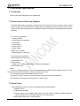
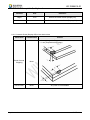
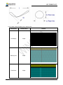
USER’S MANUAL
Part
No. :
PCB Ver. :
WL12864CA -01
V1.1
Custormer:
Standart
Customised
Wincom tech. co., Ltd
http://www.wincomlcd.com
TEL.:0755-83308729,82977087
FAX.:0755-83308659
3F, Block 13, WangJingKeng Industrial Park,DaKan XiLi, NanShan, Shenzhen City,China.
WL12864CA-01
RECORD OF REVISION
DATE
PAGE
2015-5-18
---
http://www.wincomlcd.com
SUMMARY
NEW ISSUE
PAGE:1/18
WL12864CA-01
MENU
1、
2、
3、
4、
5、
General Specifications ........................................................................................................................... 3
Pin Assignment........................................................................................................................................ 4
Block Diagram ......................................................................................................................................... 4
Outline drawing........................................................................................................................................ 5
Operation Specifications ........................................................................................................................ 6
6、
5.1 Absolute Maximum Ratings ............................................................................................................ 6
Optics & Electrical Characteristics ....................................................................................................... 7
7、
6.1 Optics Characteristics...................................................................................................................... 7
6.2 DC Characteristics ........................................................................................................................... 7
6.3 AC Characteristics............................................................................................................................ 8
Functional Specification ......................................................................................................................... 9
8、
7.1 Commands ........................................................................................................................................ 9
7.2 Power down and Power up Sequence .......................................................................................... 9
7.3 Reset Circuit...................................................................................................................................... 9
Reliability Test Items ............................................................................................................................. 10
9、
8.1 Contents of Reliability Tests.......................................................................................................... 10
8.2 Failure Check Standard ................................................................................................................. 10
Outgoing Quality Control Specifications............................................................................................ 10
10、
11、
9.1 Environment Required................................................................................................................... 10
9.2 Criteria & Acceptable Quality Level ............................................................................................. 11
Package Specifications ........................................................................................................................ 15
Precautions When Using These OEL Display Modules .................................................................. 15
11.1 Handling Precautions................................................................................................................... 15
11.2 Storage Precautions..................................................................................................................... 16
11.3 Designing Precautions................................................................................................................. 17
11.4 Precautions when disposing of the OEL display modules ..................................................... 17
11.5 Other Precautions......................................................................................................................... 17
http://www.wincomlcd.com
PAGE:2/18
WL12864CA-01
1、 General Specifications
No.
Item
Specifications
1
Display Mode
Passive Matrix
2
Display Color
Monochrome (White)
3
Drive Duty
1/64 Duty
4
Number of Pixels
128 × 64
5
Module Size
35.40 × 33.50 × 4.00 (mm)
6
Active Area (A/A)
29.42 × 14.70 (mm)
7
Pixel Pitch
0.23 × 0.23 (mm)
8
Pixel Size
0.21 × 0.21 (mm)
9
Driver IC
SSD1306
10
Mechanical Drawing
According
drawing
11
Interface
IIC
http://www.wincomlcd.com
to
the
annexed
Remark
outline
PAGE:3/18
WL12864CA-01
2、 Pin Assignment
Pin No.
1
Sysmbol
GND
I/O
Function
P
Ground of Logic Circuit
This is a ground pin. It acts as a reference for the
logic pins. It must be connected to external
ground.
Power Supply for OEL Panel
This is the most positive voltage supply pin of
the chip. It must be supplied externally.
2
VCC
P
3
SCL
I/O
The Serial Clock
4
SDA
I/O
The Serial Data
I: Input,
O: output,
Remark
P: Power
3、 Block Diagram
http://www.wincomlcd.com
PAGE:4/18
WL12864CA-01
http://www.wincomlcd.com
3
4
Pin
Symbol
4、 Outline drawing
PAGE:5/18
WL12864CA-01
5、 Operation Specifications
5.1 Absolute Maximum Ratings
Values
Item
Symbol
Min
Max
Unit
Remark
Supply Voltage for Logic
VDD
-0.3
4
V
1, 2
Supply Voltage for Display
VCC
0
15
V
1, 2
Operation Temperature
TOP
-40
70
℃
3
Storage Temperature
TSTG
-40
85
℃
3
Life Time (80 cd/m2)
30,000
hour
4
Life Time (60 cd/m2)
50,000
hour
4
Note 1: All the above voltages are on the basis of “VSS = 0V”.
Note 2: When this module is used beyond the above absolute maximum ratings, permanent
breakage of the module may occur. Also, for normal operations, it is desirable to use this
module under the conditions according to Section 3. “Optics & Electrical Characteristics”.
If this module is used beyond these conditions, malfunctioning of the module can occur
and the reliability of the module may deteriorate.
Note 3: The defined temperature ranges do not include the polarizer. The maximum withstood
temperature of the polarizer should be 80°C.
Note 4: VCC = 13.0V, Ta = 25°C, 50% Checkerboard.
End of lifetime is specified as 50% of initial brightness reached. The average operating
lifetime at room temperature is estimated by the accelerated operation at high
temperature conditions.
http://www.wincomlcd.com
PAGE:6/18
WL12864CA-01
6、 Optics & Electrical Characteristics
6.1 Optics Characteristics
Values
Characteristics
Symbol
Conditions
Unit
Min.
Typ.
Max.
cd/m2
Brightness
Lbr
Note 5
60
80
-
C.I.E. (White)
(x)
(y)
C.I.E. 1931
0.25
0.27
0.29
0.31
0.33
0.35
Dark Room
Contrast
CR
-
>10,000:1
-
free
Viewing Angle
-
degree
* Optical measurement taken at VDD = 2.8V, VCC = 13.0V.
6.2 DC Characteristics
Values
Characteristics
Symbol
Conditions
Unit
Min.
Typ.
Max.
1.65
2.8
3.3
V
Supply Voltage for
Logic
VDD
Supply Voltage for
Display
VCC
Note 5
12.5
13.0
13.5
V
High Level Input
VIH
IOUT = 100μA,
3.3MHz
0.8×VDD
-
VDD
V
Low Level Input
VIL
IOUT = 100μA,
3.3MHz
0
-
0.2×VDD
V
High Level Output
VOH
IOUT = 100μA,
3.3MHz
0.9×VDD
-
VDD
V
Low Level Output
VOL
IOUT = 100μA,
3.3MHz
0
-
0.1×VDD
V
Operating Current
for VDD
IDD
-
180
300
μA
Note 6
-
18.5
23.1
mA
Note 7
-
27.1
33.9
mA
Note 8
-
42.3
52.9
mA
Operating Current
for VCC
ICC
Sleep Mode
Current for VDD
IDD, SLEEP
-
1
5
μA
Sleep Mode
Current for VCC
ICC, SLEEP
-
2
10
μA
http://www.wincomlcd.com
PAGE:7/18
WL12864CA-01
Note 5: Brightness (Lbr) and Supply Voltage for Display (VCC) are subject to the change of the
panel characteristics and the customer’s request.
Note 6: VDD = 2.8V, VCC = 13.0V, 30% Display Area Turn on.
Note 7: VDD = 2.8V, VCC = 13.0V, 50% Display Area Turn on.
Note 8: VDD = 2.8V, VCC = 13.0V, 100% Display Area Turn on.
6.3 AC Characteristics
4.3.1 I2C Interface Timing Characteristics:
Symbol
Conditions
Min.
Max.
Unit
tcycle
Clock Cycle Time
2.5
-
μs
Start Condition Hold Time
0.6
μs
Data Hold Time (for “SDAOUT” Pin)
0
ns
tHD
Data Hold Time (for “SDAIN” Pin)
300
ns
tSD
Data Setup Time
100
ns
tSSTART
Start Condition Setup Time(Only relevant for
a repeated Start condition)
0.6
μs
tSSTOP
Stop Condition Setup Time
0.6
μs
tR
Rise Time for Data and Clock Pin
300
ns
tF
Fall Time for Data and Clock Pin
300
ns
tIDLE
Idle Time before a New Transmission can
Start
tHSTART
1.3
μs
*(VDD - VSS = 1.65V to 3.5V, Ta = 25°C)
http://www.wincomlcd.com
PAGE:8/18
WL12864CA-01
7、 Functional Specification
7.1 Commands
Refer to the Technical Manual for the SSD1309
7.2 Power down and Power up Sequence
To protect OEL panel and extend the panel life time, the driver IC power up/down routine should
include a delay period between high voltage and low voltage power sources during turn on/off. It
gives the OEL panel enough time to complete the action of charge and discharge before/after the
operation.
7.2.1 Power up Sequence:
1. Power up VDD
2. Send Display off command
3. Initialization
4. Clear Screen
5. Power up VCC
6. Delay 100ms
(When VCC is stable)
7. Send Display on command
7.2.2 Power down Sequence:
1. Send Display off command
2. Power down VCC
3. Delay 100ms
(When VCC is reach 0 and panel is completely discharges)
4. Power down VDD
Note 9:
1) Since an ESD protection circuit is connected between VDD and VCC inside the driver IC, VCC
becomes lower than VDD whenever VDD is ON and VCC is OFF.
2) VCC should be kept float (disable) when it is OFF.
3) Power Pins (VDD, VCC) can never be pulled to ground under any circumstance.
4) VDD should not be power down before VCC power down.
7.3 Reset Circuit
When RES# input is low, the chip is initialized with the following status:
1. Display is OFF
2. 128×64 Display Mode
3. Normal segment and display data column and row address mapping (SEG0 mapped to
column address 00h and COM0 mapped to row address 00h)
4. Shift register data clear in serial interface
http://www.wincomlcd.com
PAGE:9/18
WL12864CA-01
5. Display start line is set at display RAM address 0
6. Column address counter is set at 0
7. Normal scan direction of the COM outputs
8. Contrast control register is set at 7Fh
9. Normal display mode (Equivalent to A4h command)
8、 Reliability Test Items
8.1 Contents of Reliability Tests
Item
Conditions
High Temperature Operation
70℃, 240 hrs
Low Temperature Operation
-40℃, 240 hrs
High Temperature Storage
85℃, 240 hrs
Low Temperature Storage
-40℃, 240 hrs
Criteria
The operational
functions work.
High
Temperature/Humidity
60℃, 90% RH, 120 hrs
Operation
Thermal Shock
-40℃<=> 85℃, 24 cycles 60 mins dwell
* The samples used for the above tests do not include polarizer.
* No moisture condensation is observed during tests.
8.2 Failure Check Standard
After the completion of the described reliability test, the samples were left at room temperature
for 2 hrs prior to conducting the failure test at 23±5°C; 55±15% RH.
9、 Outgoing Quality Control Specifications
9.1 Environment Required
Customer’s test & measurement are required to be conducted under the following conditions:
Temperature:
23 ± 5°C
Humidity:
55 ± 15% RH
Fluorescent Lamp:
30W
Distance between the Panel & Lamp:
≥ 50cm
Distance between the Panel & Eyes of the Inspector: ≥ 30cm
Finger glove (or finger cover) must be worn by the inspector. Inspection table or jig must be
anti-electrostatic.
http://www.wincomlcd.com
PAGE:10/18
WL12864CA-01
9.2 Criteria & Acceptable Quality Level
Partition
AQL
Definition
Major
0.65
Defects in Pattern Check (Display On)
Minor
1.0
Defects in Cosmetic Check (Display Off)
9.2.1 Cosmetic Check (Display Off) in Non-Active Area
Check Item
Classification
Criteria
X > 6 mm (Along with Edge)
Y > 1 mm (Perpendicular to edge)
Panel General
Chipping
Minor
Panel Crack
Minor
http://www.wincomlcd.com
Any crack is not allowable
PAGE:11/18
WL12864CA-01
Copper
Exposed(Even
Pin or Film)
Minor
Film or Trace
Damage
Minor
Terminal Lead
Prober Mark
Acceptable
Glue
or
Contamination
on Pin(Couldn’t
Be Removed by
Alcohol)
Minor
http://www.wincomlcd.com
Not Allowable by Naked Eye Inspection
PAGE:12/18
WL12864CA-01
Ink Marking on
Back Side of
panel (Exclude
on Film)
Acceptable
Ignore for Any
9.2.2 Cosmetic Check (Display Off) in Active Area
It is recommended to execute in clear room environment (class 10k) if actual in necessary.
Check Item
Classification
Criteria
Any Dirt & Scratch on
Polarizer’s
Protective
Film
Acceptable
Ignore for not Affect the Polarizer
Scratches,
Fiber,
Line-Shape Defect
(On Polarizer)
Minor
W ≤ 0.1
W > 0.1, L ≤ 2
L>2
Dirt, Black Spot, Foreign
Material,
(On Polarizer)
Minor
Φ ≤ 0.1
0.1 < Φ ≤ 0.25
0.25 < Φ
Ignore
n≤1
n=0
Ignore
n≤1
n=0
Φ ≤ 0.5
→Ignore if no Influence on Display
0.5 < Φ
n=0
Dent, Bubbles, White
spot (Any Transparent
Spot on Polarizer)
Minor
Fingerprint, Flow Mark
(On Polarizer)
Minor
Not Allowable
* Protective film should not be tear off when cosmetic check.
** Definition of W & L & Φ (Unit: mm): Φ = (a + b) / 2
http://www.wincomlcd.com
PAGE:13/18
WL12864CA-01
9.2.3 Pattern Check (Display On) in Active Area
Check Item
Classification
No Display
Major
Missing Line
Major
Pixel Short
Major
http://www.wincomlcd.com
Criteria
PAGE:14/18
WL12864CA-01
Darker Pixel
Major
Wrong Display
Major
Un-uniform
Major
10、 Package Specifications
11、 Precautions When Using These OEL Display Modules
11.1 Handling Precautions
1) Since the display panel is being made of glass, do not apply mechanical impacts such as
dropping from a high position.
2) If the display panel is broken by some accident and the internal organic substance leaks out,
be careful not to inhale nor lick the organic substance.
3) If pressure is applied to the display surface or its neighborhood of the OEL display module, the
cell structure may be damaged and be careful not to apply pressure to these sections.
4) The polarizer covering the surface of the OEL display module is soft and easily scratched.
http://www.wincomlcd.com
PAGE:15/18
WL12864CA-01
Please be careful when handling the OEL display module.
5) When the surface of the polarizer of the OEL display module has soil, clean the surface. It
takes advantage of by using following adhesion tape.
* Scotch Mending Tape No. 810 or an equivalent Never try to breathe upon the soiled surface nor
wipe the surface using cloth containing solvent such as ethyl alcohol, since the surface of the
polarizer will become cloudy. Also, pay attention that the following liquid and solvent may spoil
the polarizer:
* Water
* Ketone
* Aromatic Solvents
6) Hold OEL display module very carefully when placing OEL display module into the system
housing. Do not apply excessive stress or pressure to OEL display module. And, do not over
bend the film with electrode pattern layouts. These stresses will influence the display
performance. Also, secure sufficient rigidity for the outer cases.
7) Do not apply stress to the driver IC and the surrounding molded sections.
8) Do not disassemble nor modify the OEL display module.
9) Do not apply input signals while the logic power is off.
10) Pay sufficient attention to the working environments when handing OEL display modules to
prevent occurrence of element breakage accidents by static electricity.
* Be sure to make human body grounding when handling OEL display modules.
* Be sure to ground tools to use or assembly such as soldering irons.
* To suppress generation of static electricity, avoid carrying out assembly work under dry
environments.
* Protective film is being applied to the surface of the display panel of the OEL display module. Be
careful since static electricity may be generated when exfoliating the protective film.
11) Protection film is being applied to the surface of the display panel and removes the protection
film before assembling it. At this time, if the OEL display module has been stored for a long
period of time, residue adhesive material of the protection film may remain on the surface of the
display panel after removed of the film. In such case, remove the residue material by the
method introduced in the above Section 5).
12) If electric current is applied when the OEL display module is being dewed or when it is placed
under high humidity environments, the electrodes may be corroded and be careful to avoid the
above.
11.2 Storage Precautions
1) When storing OEL display modules, put them in static electricity preventive bags avoiding
exposure to direct sun light nor to lights of fluorescent lamps. and, also, avoiding high
temperature and high humidity environment or low temperature (less than 0℃ environments.
http://www.wincomlcd.com
PAGE:16/18
WL12864CA-01
At that time, be careful not to let water drops adhere to the packages or bags nor let dewing
occur with them.
2) If electric current is applied when water drops are adhering to the surface of the OEL display
module, when the OEL display module is being dewed or when it is placed under high humidity
environments, the electrodes may be corroded and be careful about the above.
11.3 Designing Precautions
1) The absolute maximum ratings are the ratings which cannot be exceeded for OEL display
module, and if these values are exceeded, panel damage may be happen.
2) To prevent occurrence of malfunctioning by noise, pay attention to satisfy the VIL and VIH
specifications and, at the same time, to make the signal line cable as short as possible.
3) We recommend you to install excess current preventive unit (fuses, etc.) to the power circuit
(VDD). (Recommend value: 0.5A)
4) Pay sufficient attention to avoid occurrence of mutual noise interference with the neighboring
devices.
5) As for EMI, take necessary measures on the equipment side basically.
6) When fastening the OEL display module, fasten the external plastic housing section.
7) If power supply to the OEL display module is forcibly shut down by such errors as taking out the
main battery while the OEL display panel is in operation, we cannot guarantee the quality of this
OEL display module.
8) The electric potential to be connected to the rear face of the IC chip should be as follows:
SSD1309
* Connection (contact) to any other potential than the above may lead to rupture of the IC.
11.4 Precautions when disposing of the OEL display modules
1) Request the qualified companies to handle industrial wastes when disposing of the OEL
display modules. Or, when burning them, be sure to observe the environmental and hygienic
laws and regulations.
11.5 Other Precautions
1) When an OEL display module is operated for a long of time with fixed pattern may remain as an
after image or slight contrast deviation may occur. Nonetheless, if the operation is interrupted
and left unused for a while, normal state can be restored. Also, there will be no problem in the
reliability of the module.
2) To protect OEL display modules from performance drops by static electricity rapture, etc., do
not touch the following sections whenever possible while handling the OEL display modules.
* Pins and electrodes
* Pattern layouts such as the FPC
3) With this OEL display module, the OEL driver is being exposed. Generally speaking,
semiconductor elements change their characteristics when light is radiated according to the
principle of the solar battery. Consequently, if this OEL driver is exposed to light, malfunctioning
http://www.wincomlcd.com
PAGE:17/18
WL12864CA-01
may occur.
* Design the product and installation method so that the OEL driver may be shielded from light
in actual usage.
* Design the product and installation method so that the OEL driver may be shielded from light
during the inspection processes.
4) Although this OEL display module stores the operation state data by the commands and the
indication data, when excessive external noise, etc. enters into the module, the internal status
may be changed. It therefore is necessary to take appropriate measures to suppress noise
generation or to protect from influences of noise on the system design.
5) We recommend you to construct its software to make periodical refreshment of the operation
statuses (re-setting of the commands and re-transference of the display data) to cope wit
catastrophic noise.
Warranty:
The warranty period shall last twelve (12) months from the date of delivery. Buyer shall be
completed to assemble all the processes within the effective twelve (12) months.
Shenzhen Wincom Technology Co.,Ltd. shall be liable for replacing any products which contain defective
material or process which do not conform to the product specification, applicable drawings and
specifications during the warranty period. All products must be preserved, handled and appearance to
permit efficient handling during warranty period. The warranty coverage would be exclusive while the
returned goods are out of the terms above.
Notice:
No part of this material may be reproduces or duplicated in any form or by any means without the
written permission of Shenzhen Wincom Technology Co.,Ltd. reserves the right to make changes to this
material without notice. Shenzhen Wincom Technology Co.,Ltd. does not assume any liability of any kind
arising out of any inaccuracies contained in this material or due to its application or use in any product or
circuit and, further, there is no representation that this material is applicable to products requiring high
level reliability, such as, medical products. Moreover, no license to any intellectual property rights is
granted by implication or otherwise, and there is no representation or warranty that anything made in
accordance with this material will be free from any patent or copyright infringement of a third party. All
other product names mentioned herein are trademarks and/or registered trademarks of their respective
companies.
http://www.wincomlcd.com
PAGE:18/18