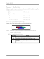
1
File No. 960-140
1
Toshiba Personal Computer
Copyright
©
1998 by Toshiba Corporation. All rights reserved. Under the copyright laws, this manual cannot be
reproduced in any form without the prior written permission of Toshiba. No patent liability is assumed with
respect to the use of the information contained herein.
Toshiba Libretto 100CT Maintenance Manual
First edition February 1998
Disclaimer
The information contained in this manual is subject to change without notice.
Toshiba Corporation and Toshiba America Information Systems, Inc., assume no liability for damages
incurred directly or indirectly from errors, omissions, or discrepancies in connection with the furnishing,
performance, or use of this material.
Trademarks
IBM is a registered trademark, and PC/AT, PS/2 and OS/2 are trademarks of IBM Corporation.
MS-DOS and Windows are registered trademarks of Microsoft Corporation.
Intel and Pentium are registered trademarks, and MMX is a trademark of Intel Corporation.
Lotus is a registered trademark of Lotus Development Corporation.
Novell and NetWare are registered trademarks of Novell, Inc.
UNIX is a registered trademark of X/Open Company Ltd.
Sound Blaster and Pro are trademarks of Creative Technology Ltd.
Centronics is a registered trademark of Centronics Data Computer Corporation.
All other properties are trademarks or registered trademarks of their respective holders.
ii
File No. 960-140
Preface
This maintenance manual describes how to perform hardware service maintenance for the
Toshiba Personal Computer Libretto 100CT.
The procedures described in this manual are intended to help service technicians isolate faulty
Field Replaceable Units (FRUs) and replace them in the field.
SAFETY PRECAUTIONS
Four types of messages are used in this manual to bring important information
to your attention. Each of these messages will be italicized and identified as
shown below.
DANGER: “Danger” indicates the existence of a hazard that could result
in death or serious injury if the safety instruction is not observed.
WARNING: “Warning” indicates the existence of a hazard that could
result in bodily injury if the safety instruction is not observed.
CAUTION: “Caution” indicates the existence of a hazard that could
result in property damage if the safety instruction is not observed.
NOTE: A Note contains general information that relates to your safe
maintenance services.
Improper repair of the computer may result in safety hazards. Toshiba requires
service technicians and authorized dealers or service providers to ensure the
following safety precautions are adhered to strictly.
Be sure to fasten screws securely with the right screwdriver. If a screw is
not fully fastened, it could loosen and create a short circuit, which could
cause overheating, smoke, or fire.
If you replace the battery pack, RTC battery, or backup battery, be sure to
use only the same model battery or an equivalent battery recommended by
Toshiba. Installation of the wrong battery can cause the battery to explode.
iii
File No. 960-140
The manual is divided into the following parts:
Chapter 1
Hardware Overview describes the system unit and each FRU.
Chapter 2
Troubleshooting Procedures explains how to diagnose and resolve
FRU problems.
Chapter 3
Tests and Diagnostics describes how to perform test and diagnostic
operations for maintenance service.
Chapter 4
Replacement Procedures describes the removal and replacement of the
FRUs.
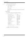
Appendices
The eight appendices describe the following:
Handling the LCD module
Board layout
Pin assignments
Keyboard scan/character codes
Key layout
Wiring diagrams
BIOS Rewrite Procedures
Reliability
iv
File No. 960-140
Conventions
This manual uses the following formats to describe, identify, and highlight terms and operating
procedures.
Acronyms
On the first appearance and whenever necessary for clarification, acronyms are
enclosed in parentheses following their definition. For example:
Read Only Memory (ROM)
Keys
Keys are used in the text to describe many operations. The keytop symbol, as it
appears on the keyboard, is printed in boldface type.
Key operation
Some operations require you to simultaneously use two or more keys. We identify
such operations by the keytop symbols separated by a plus (+) sign. For example,Ctrl
+ Pause (Break) means you must hold down Ctrl and at the same time press Pause
(Break). If three keys are used, hold down the first two and at the same time press
the third.
User input
Text that you are instructed to type in is shown in the boldface type below:
DISKCOPY A: B:
The display
Text generated by the computer that appears on its display is presented in the typeface
below:
Format complete
System transferred
v
File No. 960-140
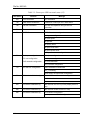
Table of Contents
Chapter 1
Hardware Overview
1.1
Features..................................................................................................................1-1
1.2
System Unit Block Diagram....................................................................................1-5
1.3
3.5-inch External FDD............................................................................................1-9
1.4
2.5-inch Hard Disk Drive......................................................................................1-10
1.5
Keyboard..............................................................................................................1-11
1.6
TFT Color LCD....................................................................................................1-12
1.7
Power Supply .......................................................................................................1-14
1.8
Batteries ...............................................................................................................1-16
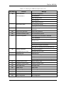
Chapter 2
Troubleshooting Procedures
2.1
Troubleshooting......................................................................................................2-1
2.2
Troubleshooting Flowchart.....................................................................................2-2
2.3
Power Supply Troubleshooting...............................................................................2-6
2.4
System Board Troubleshooting.............................................................................2-14
2.5
FDD Troubleshooting...........................................................................................2-25
2.6
HDD Troubleshooting ..........................................................................................2-28
2.7
Keyboard Troubleshooting....................................................................................2-34
2.8
Pointing Device Troubleshooting..........................................................................2-36
2.9
Display Troubleshooting.......................................................................................2-37
Chapter 3
Tests and Diagnostics
3.1
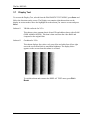
The Diagnostic Test................................................................................................3-1
3.2
Executing the Diagnostic Test.................................................................................3-3
3.3
Subtest Names........................................................................................................3-7
3.4
System Test............................................................................................................3-9
3.5
Memory Test ........................................................................................................3-10
3.6
Keyboard Test ......................................................................................................3-12
vi
File No. 960-140
3.7
Display Test..........................................................................................................3-16
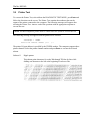
3.8
Floppy Disk Test ..................................................................................................3-20
3.9
Printer Test...........................................................................................................3-22
3.10
Async Test............................................................................................................3-24
3.11
Hard Disk Test .....................................................................................................3-26
3.12
Real Timer Test....................................................................................................3-30
3.13
NDP Test .............................................................................................................3-32
3.14
Expansion Test .....................................................................................................3-33
3.15
Sound Test ...........................................................................................................3-35
3.16
Error Code and Error Status Names......................................................................3-36
3.17
Hard Disk Test Detail Status.................................................................................3-39
3.18
Hard Disk Format.................................................................................................3-41
3.19
Head Cleaning ......................................................................................................3-46
3.20
Log Utilities..........................................................................................................3-47
3.21
Running Test ........................................................................................................3-49
3.22
Floppy Disk Drive Utilities....................................................................................3-51
3.23
System Configuration............................................................................................3-56
3.24
SETUP.................................................................................................................3-58
Chapter 4
Replacement Procedures
4.1
Overview................................................................................................................4-1
4.2
HDD.......................................................................................................................4-8
4.3
Optional Memory Module.....................................................................................4-10
4.4
Keyboard..............................................................................................................4-12
4.5
Display Assembly..................................................................................................4-13
4.6
RTC Battery.........................................................................................................4-17
4.7
System Board, Heat Sink and PC Card Slot..........................................................4-18
4.8
Display Mask........................................................................................................4-20
4.9
FL Inverter Board.................................................................................................4-22
4.10
LCD Module ........................................................................................................4-24
4.11
Speaker, Power Switch Board and AccuPoint Board.............................................4-27
4.12
LCD Flexible Cable and Microphone.....................................................................4-30
vii
File No. 960-140
4.13
I/O Adapter Board................................................................................................4-35
Appendices
Appendix A
Handling the LCD Module ......................................................................... A-1
Appendix B
Board Layout.............................................................................................B-1
Appendix C
Pin Assignments......................................................................................... C-1
Appendix D
Keyboard Scan/Character Codes ................................................................D-1
Appendix E
Key Layout ................................................................................................ E-1
Appendix F
Wiring Diagrams .........................................................................................F-1
Appendix G
BIOS Rewrite Procedures ..........................................................................G-1
Appendix H
Reliability...................................................................................................H-1
viii
File No. 960-140
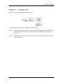
Chapter 1
Hardware Overview
File No. 960-140
1-ii
File No. 960-140
Chapter 1
Contents
1.1
Features..................................................................................................................1-1
1.2
System Unit Block Diagram....................................................................................1-5
1.3
3.5-inch External FDD............................................................................................1-9
1.4
2.5-inch Hard Disk Drive......................................................................................1-10
1.5
Keyboard..............................................................................................................1-11
1.6
TFT Color LCD....................................................................................................1-12
1.6.1
TFT Color LCD Module..................................................................1-12
1.6.2
FL Inverter Board ............................................................................1-13
1.7
Power Supply .......................................................................................................1-14
1.8
Batteries ...............................................................................................................1-16
1.8.1
Main Battery....................................................................................1-16
1.8.2
Battery Icon.....................................................................................1-16
1.8.3
Battery Charging Control.................................................................1-17
1.8.4
RTC Battery ....................................................................................1-17
Figures
Figure 1-1 Front of the computer........................................................................................1-4
Figure 1-2 System unit configuration..................................................................................1-4
Figure 1-3 System unit block diagram.................................................................................1-5
Figure 1-4 3.5-inch FDD ...................................................................................................1-9
Figure 1-5 2.5-inch HDD.................................................................................................1-10
Figure 1-6 Keyboard .......................................................................................................1-11
Figure 1-7 TFT color LCD..............................................................................................1-12
1-iii
File No. 960-140
Tables
Table 1-1 3.5-inch FDD specifications...............................................................................1-9
Table 1-2 2.5-inch HDD specifications..............................................................................1-9
Table 1-3 LCD specifications...........................................................................................1-12
Table 1-4 FL inverter board specifications.......................................................................1-13
Table 1-5 Power supply board output rating....................................................................1-15
Table 1-6 Battery specifications........................................................................................1-16
Table 1-7 Time required for quick charges........................................................................1-17
Table 1-8 RTC battery charging/data preservation time...................................................1-17
1-iv
File No. 960-140
1
Features
1.1
Features
The computer uses Toshiba's advanced Large Scale Integration (LSI), and Complementary
Metal-Oxide Semiconductor (CMOS) technology extensively to provide compact size,
minimum weight, low power usage and high reliability. This computer incorporates the
following features and benefits:
Microprocessor
The computer is equipped with an Intel® Pentium® processor with
MMX Technology that operates at 166MHz and 1.8/2.5 volts.
Memory
The computer comes with 32MB of Extend Data Out (EDO) DRAM.
HDD
The computer has a 2.5-inch HDD with a capacity of 2.1GB HDD or 3.2GB HDD.
Display
The computer has a 7.1-inch color, Thin Film Transistor (TFT) Liquid Crystal
Display (LCD), that enables display up to 256K colors at a resolution 800 x 480
pixels.
A video controller and 2MB of VRAM enable an external monitor to display 16M
colors at a resolution of 800 x 600 pixels or 64K colors at a resolution of 1024 x
768 pixels.
Keyboard
An-easy-to-use 80/82-key keyboard provides a numeric keypad overlay for fast
numeric data entry or for cursor and page control. The keyboard also includes two
keys that have special functions in Microsoft® Windows® 95. It supports software
that uses a 101- or 102-key enhanced keyboard.
Batteries
The computer has two batteries a Lithium-Ion main battery pack and RTC battery
that backs up the Real Time Clock and CMOS memory.
Expansion memory slot
An optional 32MB memory module can be installed in the memory slot.
1-1
File No. 960-140
Universal Serial Bus (USB)
The USB enables daisy-chain connection of up to 127 USB-equipped devices and
12Mbps serial data transfer. It is designed for easy configuration by a PnP
operating system and provides hot insertion/ejection capability. The USB port is
only on the Enhanced Port Replicator.
External monitor port
The port is available only on the I/O adapter and enables connection of an external
SVGA compatible monitor.
PC card slot
A PC card slot accommodates two 5mm cards (Type II) or one 10.5mm (Type III)
card, which support the PC card Standard. These slots support an external FDD,
16-bit PC cards and CardBus PC cards (32 bit) as well as the Zoomed Video (ZV)
port cards, which are dedicated to high-performance video data transfer such as
MPEG video play back.
AccuPoint
This pointer control stick, located in the right of the display panel, provides
convenient control of the cursor without requiring desk space for a mouse.
Docking interface
A 140-pin, docking interface port enables connection of the I/O adapter or an
optional Enhanced Port Replicator.
The Enhanced Port Replicator has two additional PC card slots that one
accommodates a 10.5mm card (Type III) and one accommodates a 5mm card
(Type II). These slots support CardBus PC card. The Enhanced Port Replicator
also has PS/2 mouse, PS/2 compatible keyboard, USB, parallel, serial and
external monitor ports.
Infrared port
The infrared port is compatible with Fast InfraRed (FIR) standards enabling
wireless 4Mbps data transfer with Infrared Data Association (IrDA) 1.1 compatible
devices.
Sound system
A Sound Blaster Pro and Windows Sound System compatible sound system
gives the computer multimedia capability. The sound system is equipped with
speaker, microphone and stereo headphone jack.
1-2
File No. 960-140
External FDD
A 3.5-inch external FDD is connected to the PC card slot and accommodates both
2HD (1.44MB) and 2DD (720KB) disks.
1-3
File No. 960-140
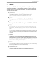
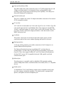
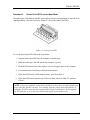
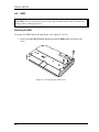
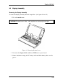
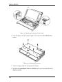
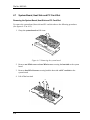
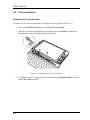
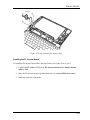
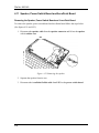
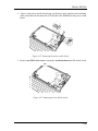
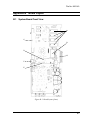
The computer is shown in Figure 1-1. The system unit configuration is shown in Figure 12.
Figure 1-1 Front of the computer
Figure 1-2 System unit configuration
1-4
File No. 960-140
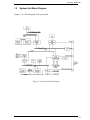
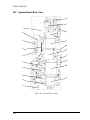
1.2
System Unit Block Diagram
Figure 1-3 is a block diagram of the system unit.
Figure 1-3 System unit block diagram
1-5
File No. 960-140
The system unit is composed of the following major components:
Intel Pentium processor
Intel 166MHz Pentium processor with MMX Technology.
The math co-processor and 32KB cache memory are integrated into the Pentium.
Standard RAM
•
•
•
•
•
32 MB, four 4M x 16-bit EDO DRAM chips
3.3 volt operation
No parity bit
Access time 60 ns
Data transfer is 64-bit width
BIOS ROM (Flash EEPROM)
•
•
•
•
512 KB, one 512K x 8-bit chip
− 256 KB are used for system BIOS
− 64 KB are used for VGA-BIOS
− 8 KB are used for plug and play data area
− 8 KB are used for password security
− 16 KB are used for boot strap
− 288 KB are reserved
5 volt operation
Access time 120 ns
Data transfer is 8-bit width
Optional memory
One expansion memory slot is available for 32MB memory modules. The 32MB
memory modules consist of four 4M x 16-bit EDO DRAM chips.
•
•
•
•
1-6
3.3 volt operation
No parity bit
Access time 60 ns
Data transfer is 64-bit width
File No. 960-140
System Controller Gate Array
•
This gate array has the following functions:
− CPU interface/control
− DRAM control
− PCI master/slave interface
− Write buffer (CPU-DRAM, CPU-PCI, PCI-DRAM)
− Prefetch buffer (CPU-PCI, PCI-DRAM)
− Mobile-PC/PCI support DMA function
− Serial interrupt function
− Power management control
− Suspend/resume control
− CPU stop clock function
− PCI clock stop function
− ACPI support function
I/O & PC Card Controller Gate Array
•
This gate array has the following functions:
− One UARTs 16550A equivalent (One SIO is used for SIR.)
− One parallel port control supported ECP
− mini ISA bus control
− PCI bus front end control
− PC card control
− ZV-port support
− CardBus control
− FIR function
− Universal I/O port
− Beep volume
− Speaker control
− RTC One T9934 chip is used
Video Controller
•
The NeoMagic NM2160 chip is used. The Video controller incorporates
2MB of video memory using a 128-bit data path.
Keyboard Controller (KBC)
•
One M38813S chip is used. This KBC includes the keyboard scan
controller and keyboard interface controller. The KBC controls the internal
keyboard, external keyboard, AccuPoint and PS/2 mouse.
AccuPoint Controller (IPSC)
•
•
One EMEP 010B chip is used.
This controller provides simultaneous control of the Pointing Device.
1-7
File No. 960-140
Sound Controller
•
•
1-8
One OPL3-SA3 is used.
The OPL3-SA3 incorporates OPL3 FM synthesizer, Digital Analog
Converter (DAC) and MPU401 MIDI interface.
File No. 960-140
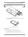
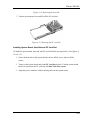
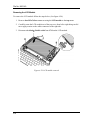
1.3
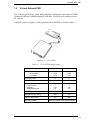
3.5-inch External FDD
The 3.5inch external FDD is a thin, high performance reliable drive that supports 720KB
(formatted) 2DD and 1.44MB (formatted) 2HD disks. The FDD can be connected to the
PC card slot.
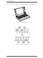
The FDD is shown in Figure 1-4. The specifications for the FDD are listed in Table 1-1.
Figure 1-4 3.5-inch FDD
Table 1-1 3.5-inch FDD specifications
Item
2-MB mode
1-MB mode
2,000
1,440
1,000
720
Number of heads
2
2
Number of cylinders
80
80
Access time (ms)
Track to track
Average
Head settling time
3
181
15
3
181
15
Recording track density (tpi)
135
135
Data transfer rate (Kbps)
500
250
Rotation speed (rpm)
300
300
Storage capacity (KB)
Unformatted
Formatted
Recording method
Modified Frequency Modulation (MFM)
1-9
File No. 960-140
1.4
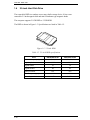
2.5-inch Hard Disk Drive
The removable HDD is a random access non-volatile storage device. It has a nonremovable 2.5-inch magnetic disk and mini-Winchester type magnetic heads.
The computer supports 2.1GB HDD or 3.2GB HDD.
The HDD is shown in Figure 1-5. Specifications are listed in Table 1-2.
Figure 1-5 2.5-inch HDD
Table 1-2 2.5-inch HDD specifications
Items
IBM DYKA-22160
IBM DYKA-23240
2,167,603,200
3,253,469,184
4,200
6,304
Logical heads
16
16
Logical sectors
63
63
Bytes per sector
512
512
4,200
4,200
8-9 RLL
8-9 RLL
Formatted capacity (bytes)
Logical cylinders
Rotation speed (rpm)
Recording method
1-10
File No. 960-140
1.5
Keyboard
The 84-(USA) or 86-(European) key keyboard is mounted on the system unit. The
keyboard is connected to the keyboard controller on the system board through a 24-pin
flat cable. The keyboard is shown in Figure 1-6.
See Appendix E for optional keyboard configurations.
Figure 1-6 Keyboard
1-11
File No. 960-140
1.6
TFT Color LCD
The display panel contains a TFT color LCD module, a fluorescent lamp (FL) andan FL
inverter board.
1.6.1 TFT Color LCD Module
The LCD enables display of up to 256K colors at a resolution 800 x 480 pixels.
The LCD is shown in Figure 1-7. Specifications are listed in Table 1-3.
Figure 1-7 TFT color LCD
Table 1-3 LCD specifications
Items
Number of Pixels
Dot pitch
(mm)
Display area
Contrast
1-12
(pixels)
(mm)
Specifications
800x480
0.192x0.192
153.6(H)x92.16(V)
1:150 (Typ)
File No. 960-140
1.6.2 FL Inverter Board
The FL inverter board supplies high frequency current to light the LCD’s Fluorescent
Lamp.
Specifications for the FL inverter are listed in Table 1-4.
Table 1-4 FL inverter board specifications
Item
Specifications
Input
Voltage
Power
(V)
(W)
Output
Voltage
Current
(Vrms)
(mA)
*NOTE: The FL currents at power on are:
Level 3 : 3.5mA
Level 2 : 2.9mA
5
2.3
800
2.0 to 3.5*
Level 1 : 2.6mA
Level 0 : 2.0mA
1-13
File No. 960-140
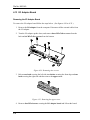
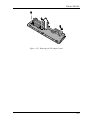
1.7
Power Supply
The power supply supplies ten kinds of voltages to the system board, has one
microprocessor and it operates at 4MHz. It performs the following functions:
1. Determines if the AC adapter or battery is connected to the computer.
2. Detects DC output and circuit malfunctions.
3. Controls the battery icon, and DC IN icon.
4. Turns the battery charging system on and off and detects a fully charged battery.
5. Determines if the power can be turned on and off.
6. Provides more accurate detection of a low battery.
7. Calculates the remaining battery capacity.
The embedded controller operates at 2MHz and has the following functions:
1. Controls ACPI in Windows 98.
2. Monitors the computer’s temperature.
3. Controls power supply to the docking port.
4. General purpose port.
1-14
File No. 960-140
The power supply output rating is specified in Table 1-5.
Table 1-5 Power supply board output rating
Power supplied Yes/No
Use
Name
Voltage(V)
Suspend
Power off
No battery
CPU
+1.8V
1.8
NO
NO
NO
CPU, CLKGEN, System
Controller GA
+2.5V
2.5
NO
NO
NO
CLKGEN
+3.3V
3.3
NO
NO
NO
System Controller GA, PC
Card Slot, VGA Controller,
I/O & PC Card Controller
GA, DRAM
B3V
3.3
YES
NO
NO
VGA Controller, PC Card
Slot
B5V
5.0
YES
NO
NO
Flash Memory, KBC, IPSC,
LCD Panel, HDD, LEDs,
Sound, E2PROM,GA
VCC
5.0
NO
NO
NO
IFVCC
5.0
NO
NO
NO
PSC
MCV
5.0
YES
YES
NO
Embedded Controller
S5V
5.0
YES
YES
NO
RTCV
5.0
YES
YES
YES
KB/Mouse Port
RTC
1-15
File No. 960-140
1.8
Batteries
The computer has tow types of batteries:
Main battery pack
RTC battery
The battery specifications are listed in Table 1-6.
Table 1-6 Battery specifications
Battery name
Material
Output voltage
Capacity
Main battery
Lithium-Ion
10.8 V
1,200 mAh
2,400 mAh (High capacity)
RTC battery
Nickel Metal Hydride
2.4 V
11 mAh
1.8.1 Main Battery
The removable main battery pack is the computer’s main power source when the Universal
AC Adapter is not connected. The main battery pack maintains the state of the computer
when the computer enters in resume mode.
1.8.2 Battery Icon
The icon shows the status of the removable battery pack.
The status of each can be determined by color:
Orange
Green
Blinking orange
No light
1-16
The battery is being charged. (Universal AC Adapter connected)
The battery is full charged. (Universal AC Adapter connected)
The battery is low when the power is on.
Under any other conditions, the LED does not light.
File No. 960-140
1.8.3 Battery Charging Control
Battery charging is controlled by a power supply microprocessor that is mounted on the
system board. The microprocessor controls whether the charge is on or off and detects a
full charge when the Universal AC Adapter and battery are connected to the computer.
The system charges the battery using quick charge or trickle charge.
Quick Battery Charge
The battery quick charges when the Universal AC Adapter is connected and the
system is powered off or in suspend mode.
Table 1-7 Time required for quick charges
Status
Charging time
Quick charge 1(power off)
2 to 3 hours
Quick charge 2(power on)
5 to 6 hours
If any of the following occurs, the Main Battery quick charge process stops.
1. The Main Battery becomes fully charged.
2. The AC adapter or Main Battery is removed.
3. The Main Battery or output voltage is abnormal.
Trickle Battery Charge
When the main battery is fully charged and the AC adapter is attached, the
microprocessor automatically changes quick charge 1 or 2 to trickle charge.
1.8.4 RTC Battery
The RTC battery provides power to keep the current date, time and other setup
information in memory while the computer is turned off. Table 1-8 lists the charging time
and data preservation period of the RTC battery.
Table 1-8 RTC battery charging/data preservation time
Status
Time
Charging Time
48 hours
Data preservation period (full charge)
1 month
1-17
File No. 960-140
1-18
File No. 960-140
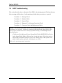
Chapter 2
Troubleshooting Procedures
File No. 960-140
2-ii
File No. 960-140
Chapter 2
Contents
2.1
Troubleshooting......................................................................................................2-1
2.2
Troubleshooting Flowchart.....................................................................................2-2
2.3
Power Supply Troubleshooting...............................................................................2-6
2.4
2.5
2.6
2.7
Procedure 1
Power Status Check.............................................................2-6
Procedure 2
Error Code Check................................................................2-8
Procedure 3
Connection Check..............................................................2-11
Procedure 4
Quick Charge Check ..........................................................2-12
Procedure 5
Replacement Check............................................................2-13
System Board Troubleshooting.............................................................................2-14
Procedure 1
Message Check ..................................................................2-15
Procedure 2
Printer Port LED Check on Boot Mode..............................2-17
Procedure 3
Printer Port LED Check on Resume Mode.........................2-23
Procedure 4
Diagnostic Test Program Execution Check.........................2-24
Procedure 5
Replacement Check............................................................2-24
FDD Troubleshooting...........................................................................................2-25
Procedure 1
FDD Head Cleaning Check ................................................2-25
Procedure 2
Diagnostic Test Program Execution Check.........................2-26
Procedure 3
Connector Check and Replacement Check..........................2-27
HDD Troubleshooting ..........................................................................................2-28
Procedure 1
Message Check ..................................................................2-29
Procedure 2
Partition Check ..................................................................2-30
Procedure 3
Format Check ....................................................................2-31
Procedure 4
Diagnostic Test Program Execution Check.........................2-32
Procedure 5
Connector Check and Replacement Check..........................2-33
Keyboard Troubleshooting....................................................................................2-34
Procedure 1
Diagnostic Test Program Execution Check.........................2-34
Procedure 2
Connector and Replacement Check....................................2-35
2-iii
File No. 960-140
2.8
2.9
Pointing Device Troubleshooting..........................................................................2-36
Procedure 1
Diagnostic Test Program Execution Check.........................2-36
Procedure 2
Connector and Replacement Check ....................................2-36
Display Troubleshooting.......................................................................................2-37
Procedure 1
Diagnostic Test Program Execution Check.........................2-37
Procedure 2
Connector and Replacement Check....................................2-38
Figures
Figure 2-1 Troubleshooting flowchart ...............................................................................2-3
Figure 2-2 Printer port LED............................................................................................2-17
Tables
Table 2-1 Battery icon.......................................................................................................2-6
Table 2-2 DC IN icon........................................................................................................2-7
Table 2-3 Printer port LED boot mode status .................................................................2-18
Table 2-4 Printer port LED Resume mode error status.....................................................2-23
Table 2-5 FDD error code and status...............................................................................2-26
Table 2-6 Hard disk drive error code and status...............................................................2-32
2-iv
File No. 960-140
1
1.1
Troubleshooting
Chapter 2 describes how to determine if a Field Replaceable Unit (FRU) in the computer is
causing the computer to malfunction. The FRUs covered are:
1. System Board
4. Hard Disk Drive
2. FL Inverter Board
5. Keyboard
3. Floppy Disk Drive
6. Display
7. Pointing Board
The Diagnostics Disk operations are described in Chapter 3. Detailed replacement procedures
are given in Chapter 4.
The following tools are necessary for implementing the troubleshooting procedures:
1. Diagnostics Disk
2. Phillips screwdriver (2 mm)
3. Toshiba MS-DOS system disk(s)
(You must install the following onto the disk: SYS.COM, FORMAT.COM,
FDISK.COM and FDISK.EXE)
4. 2DD or 2HD formatted work disk for floppy disk drive testing
5. Cleaning kit for floppy disk drive troubleshooting
6. Printer port LED
7. Printer port wraparound connector
8. Serial port wraparound connector
9. PC card wraparound card
10. Multimeter
11. I/O Adapter
12. External FDD
1-1
File No. 960-140
1.2
Troubleshooting Flowchart
Use the flowchart in Figure 2-1 as a guide for determining which troubleshooting procedures
to execute. Before going through the flowchart steps, verify the following:
Ask the user if a password is registered and, if it is, ask him or her to enter the
password. If the user has forgotten the system password, perform the following
procedure at the appropriate step in the flowchart in Figure 2-1:
Connect the printer port wraparound board (F31PRT), then turn the POWER switch
on. The computer will override the password function by erasing the current
password.
®
Verify with the customer that Toshiba Windows 95 is installed on the hard disk. NonToshiba operating systems can cause the computer to malfunction.
Make sure all optional equipment is removed from the computer.
Make sure the floppy disk drive is empty.
1-2
File No. 960-140
Figure 2-1 Troubleshooting flowchart (1/2)
1-3
File No. 960-140
Figure 2-1 Troubleshooting flowchart (2/2)
If the diagnostics program cannot detect an error, the problem may be intermittent. The
Running Test program should be executed several times to isolate the problem. Check the
Log Utilities function to confirm which diagnostic test detected an error, then perform the
appropriate troubleshooting procedures as follows:
1. If an error is detected on the system test, memory test, display test, async test, printer
test, expansion test, sound test or real timer test, perform the System Board
Troubleshooting Procedures in Section 2.4.
2. If an error is detected on the floppy disk test, perform the FDD Troubleshooting
Procedures in Section 2.5.
3. If an error is detected on the hard disk test, perform the HDD Troubleshooting
Procedures in Section 2.6.
1-4
File No. 960-140
4. If an error is detected on the keyboard test, perform the Keyboard Troubleshooting
Procedures in Section 2.7.
5. If an error is detected on the display test, perform the Display Troubleshooting
Procedures in Section 2.9.
1-5
File No. 960-140
1.3
Power Supply Troubleshooting
The power supply controls many functions and components. To determine if the power supply
is functioning properly, start with Procedure 1 and continue with the other Procedures as
instructed. The procedures described in this section are:
Procedure 1: Power Status Check
Procedure 2: Error Code Check
Procedure 3: Connection Check
Procedure 4: Quick Charge Check
Procedure 5: Replacement Check
Procedure 1
Power Status Check
The following icons indicate the power supply status:
Battery icon
DC IN icon
The power supply controller displays the power supply status through the Battery and the DC
IN icons as listed in the tables below.
Table 2-1 Battery icon
Battery icon
Power supply status
Lights orange
Quick charge
Lights green
Battery is fully charged and AC adapter is connected
Blinks orange
(even intervals)
The battery level becomes low while operating the computer on battery
power.*1
Flashes orange
*2
The power switch is pressed on when the battery level is low.
Doesn’t light
Any condition other than those above.
*1 Auto Hibernation Off will be executed soon.
*2 Auto Hibernation Off has already been executed.
1-6
File No. 960-140
Table 2-2 DC IN icon
DC IN icon
Power supply status
Lights green
DC power is being supplied from the AC adapter.
Blinks orange
Power supply malfunction*3
Doesn’t light
Any condition other than those above.
*3 When the power supply controller detects a malfunction, the DC IN icon blinks
and an error code is displayed.
To check the power supply status, install a battery pack and connect an AC adapter.
Check 1
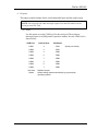
If the DC IN icon blinks orange, go to Procedure 2.
Check 2
If the DC IN icon does not light, go to Procedure 3.
Check 3
If the battery icon does not light orange or green, go to Procedure 4.
CAUTION: Use only an AC adapter manufactured for the Libretto 100CT. If you use
another AC adapter, the computer's power supply may malfunction or a fuse on the
system board may be blown.
1-7
File No. 960-140
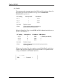
Procedure 2
Error Code Check
If the power supply microprocessor detects a malfunction, the DC IN icon blinks orange. The
blink pattern indicates an error as shown below.
Start
Off for 2 seconds
Error code (8 bit)
“1”
On for one second
“0”
On for half second
Interval between data bits
Off for half second
The error code begins with the least significant digit.
Example: Error code 12h (Error codes are given in hexadecimal format.)
Check 1
Convert the DC IN icon blink pattern into the hexadecimal error code and
compare it to the tables below.
DC power supplied through AC adapter
Error code
1-8
Meaning
10h
AC Adapter voltage is over 16.5V (15V+10%).
12h
Current from the DC power supply is over the limit (3.13A).
13h
Current from the DC power supply is over the limit (0.5A) when there
is no load.
14h
Current sensing IC is not normal.
File No. 960-140
Main Battery
Error code
Meaning
20h
Battery voltage is over the limit (13.46V).
21h
Main battery charge current is over the limit (2.53A).
22h
Mai battery discharge current is over the maximum allowed limit when
there is no load (0.5A).
23h
Main battery charge current is over limit (1.80A) whenthere .
24h
Current sensing IC is not normal.
25h
Main battery charge current is over the limit (0.5A).
S5V output
Error code
40h
Meaning
S5V voltage is under the limit (4.75V).
B5V output
Error code
Meaning
50h
B5V voltage is over the limit (5.5V).
51h
B5V voltage is under the limit (4.5V) when power supply is turned on.
52h
B5V voltage is under the limit (4.5V) when the computer is booting up.
53h
B5V dose not start up when the computer is suspended.
B3V output
Error code
Meaning
60h
B3V voltage is over the limit (3.8V).
61h
B3V voltage is under the limit (2.81V) when power supply is turned on.
62h
B3V voltage is under the limit (2.81V) when the computer is booting
up.
63h
B3V dose not start up when the computer is suspended.
1-9
File No. 960-140
B2V output
Error code
Meaning
70h
B2V voltage is over the limit (2.88V).
71h
B2V voltage is under the limit (2.13V) when power supply is turned on.
72h
B2V voltage is under the limit (2.13V) when the computer is booting
up.
73h
B2V voltage is over the limit (2.13V) when power supply is turned off.
B1V output
Error code
Check 2
Meaning
80h
B1V voltage is over the limit (2.16V).
81h
B1V voltage is under the limit (1.44V) when power supply is turned on.
82h
B1V voltage is under the limit (1.44V) when the computer is booting
up.
83h
B1V voltage is over the limit (1.44V) when power supply is turned off.
In the case of error code 10h:
Make sure the AC adapter is firmly connected to the computer is DC IN
socket and to power source. If this cables are connected correctly, go to the
following step:
Replace the AC adapter with a new one. If the error still exists, go to
Procedure 5.
Check 3
In the case of error code 20h:
Make sure the battery pack is correctly installed in the computer. If the battery
pack is correctly installed, go to the following step:
Replace the battery pack with a new one. If the error still exists, go to
Procedure 5.
Check 4
In the case of error code 21h:
Go to Procedure 3.
Check 5
1-10
When for any other error, go to Procedure 5.
File No. 960-140
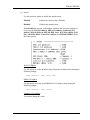
Procedure 3
Connection Check
The power supply wiring diagram is shown below:
Any of the connectors may be disconnected. Perform Check 1.
Check 1
Make sure the Libretto 100's AC adapter is firmly connected to the computer's DC
IN socket and a power source. If these cables are connected correctly, go to
Check 2.
Check 2
Replace the AC adapter with a new one. If the DC IN icon does not glow green,
go to Procedure 5.
1-11
File No. 960-140
Procedure 4
Quick Charge Check
The power supply may not charge the battery pack. Perform the following procedures:
1. Reinstall the battery pack.
2. Attach the AC adapter and turn on the power. If you cannot turn on the power, go to
Procedure 5.
3. Run the Diagnostic test, go to System test and execute subtest 06 (quick charge)
described in Chapter 3.
4. When quick charge is complete, the diagnostics test displays the result code. Check
the result code against the table below and perform any necessary check.
Result code
Contents
Check items
0
The battery is quick charging normally.
Normal
1
The battery is fully charged.
Normal
2
The AC adapter is not attached.
Check 1
3
The AC adapter’s output voltage is not normal.
Check 1
4
The Battery is not installed.
Check 2
5
The battery’s output voltage is not normal.
Check 3
6
The battery’s temperature is not normal.
Check 4
7
A bad battery is installed.
Check 2
8
Any other problems.
Check 5
Check 1
Make sure the AC adapter and AC power cord are firmly plugged into the DC IN
socket and the wall outlet. If these cables are connected correctly, replace the AC
power cord and AC adapter.
Check 2
Make sure the battery is properly installed. If the battery is properly installed,
replace it with a new one.
Check 3
The battery pack may be completely discharged. Wait a few minutes to charge the
battery pack. If the battery pack is still not charged, replace the battery pack with a
new one.
Check 4
The battery’s temperature is too hot or cold. Return the temperature to a normal
operating condition. If the battery pack still is not charged, replace the battery
pack with a new one.
Check 5
Go to Procedure 5.
1-12
File No. 960-140
Procedure 5
Replacement Check
The AC adapter may be disconnected or damaged. Disassemble the computer following the
steps described in Chapter 4, Replacement Procedures. After checking the connection,
perform the following checks:
Check 1
Replace the AC adapter with a new one. If the problem still exists, go to Check 2.
Check 2
Replace the system board with a new one. Refer to Chapter 4 for instructions on
how to remove and replace the system board.
1-13
File No. 960-140
1.4
System Board Troubleshooting
This section describes how to determine if the system board is defective or not functioning
properly. Start with Procedure 1 and continue with the other procedures as instructed. The
procedures described in this section are:
Procedure 1: Message Check
Procedure 2: Printer Port LED Check on Boot Mode
Procedure 3: Printer Port LED Check on Resume Mode
Procedure 4: Diagnostic Test Program Execution Check
Procedure 5: Replacement Check
1-14
File No. 960-140
Procedure 1
Message Check
When the power is turned on, the system performs the Initial Reliability Test (IRT) installed in
the BIOS ROM. The IRT tests each IC on the system board and initializes it.
If an error message is shown on the display, perform Check 1.
If there is no error message, go to Procedure 2.
If Toshiba MS-DOS or Toshiba Windows 95 is properly loaded, go to Procedure 4.
Check 1
If one of the following error messages displays on the screen, press the F1 key as
the message instructs. These errors occur when the system configuration preserved
in the RTC memory (CMOS type memory) is not the same as the actual
configuration or when the data is lost.
If you press the F1 key as the message instructs, the TSETUP screen appears to
set the system configuration. If error message (b) appears often when the power is
turned on, replace the RTC battery. If any other error message displays, perform
Check 2.
(a)
(b)
(c)
(d)
(e)
(f)
(g)
Check 2
*** Bad HDD type ***
Check system. Then press [F1] key
......
*** Bad RTC battery ***
Check system.
Then press [F1] key
......
*** Bad configuration ***
Check system. Then press [F1] key
......
*** Bad memory size ***
Check system. Then press [F1] key
......
*** Bad time function ***
Check system. Then press [F1] key
......
*** Bad check sum (CMOS) ***
Check system. Then press [F1] key
......
*** Bad check sum (ROM) ***
Check system. Then press [F1] key
......
If the following error message displays on the screen, press any key as the message
instructs. If any other error message displays, perform Check 3.
The following error message appears when data stored in RAM under the resume
function is lost because the battery has become discharged or the system board is
damaged. Go to Procedure 3.
WARNING:
RESUME FAILURE.
PRESS ANY KEY TO CONTINUE.
1-15
File No. 960-140
Check 3
The IRT checks the system board. When the IRT detects an error, the system
stops or an error message appears.
If one of the following error messages (1) through (17), (24) or (25) displays, go
to Procedure 5.
If error message (18) displays, go to the Keyboard Troubleshooting Procedures in
Section 2.7.
If error message (19), (20) or (21) displays, go to the HDD Troubleshooting
Procedures in Section 2.6.
If error message (22) or (23) displays, go to the FDD Troubleshooting Procedures
in Section 2.5.
(1)
(2)
(3)
(4)
(5)
(6)
(7)
(8)
(9)
(10)
(11)
(12)
(13)
(14)
(15)
(16)
(17)
(18)
(19)
(20)
(21)
(22)
(23)
(24)
(25)
1-16
PIT ERROR
MEMORY REFRESH ERROR
TIMER CH.2 OUT ERROR
CMOS CHECKSUM ERROR
CMOS BAD BATTERY ERROR
FIRST 64KB MEMORY ERROR
FIRST 64KB MEMORY PARITY ERROR
VRAM ERROR
SYSTEM MEMORY ERROR
SYSTEM MEMORY PARITY ERROR
EXTENDED MEMORY ERROR
EXTENDED MEMORY PARITY ERROR
DMA PAGE REGISTER ERROR
DMAC #1 ERROR
DMAC #2 ERROR
PIC #1 ERROR
PIC #2 ERROR
KBC ERROR
HDC ERROR
HDD #0 ERROR
HDD #1 ERROR
NO FDD ERROR
FDC ERROR
TIMER INTERRUPT ERROR
RTC UPDATE ERROR
File No. 960-140
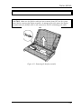
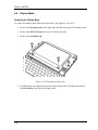
Procedure 2
Printer Port LED Check on Boot Mode
The printer port LED displays the IRT status and test status by turning lights on and off as an
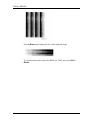
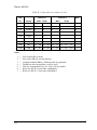
eight-digit binary value for boot mode. Figure 2-2 shows the printer port LED.
Figure 2-2 Printer port LED
To use the printer port LED follow the steps below:
1. Plug the printer port LED into the computer’s parallel port.
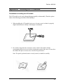
2. Hold down the space bar and turn on the computer’s power.
3. Read the LED status from left to right as you are facing the back of the computer.
4. Convert the status from binary to hexadecimal notation.
5. If the final LED status is FFh (normal status), go to Procedure 4.
6. If the final LED status matches any of the test status values in Table 2-3, perform
Check 1.
NOTE: If an error condition is detected by the IRT test, the printer port LED displays an
error code after the IRT test ends. For example, when the printer port LED displays 1F
and halts, the IRT test has already completed the Display initialization. In this instance,
the IRT indicates an error has been detected during the system memory test.
1-17
File No. 960-140
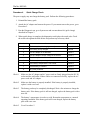
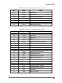
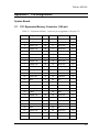
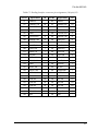
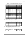
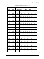
Table 2-3 Printer port LED boot mode status (1/5)
LED Status
Test item
Message
FFh
Start
Register initialization for boot block
B0h
Flash ROM check
PIT ch.0 initialization
BIOS rewrite flag initialization
Transition to protected mode
Boot block checksum
KBC initialization
BIOS (runtime and IRT) checksum
B2h
KBC initialization (1)
KBC initialization
B3h
BIOS rewrite
BIOS rewrite request check
Canceling power down of L2-cache
Enabling CMOS access
Port 25h unlock
00h
Special register initialization
Toshiba register initialization (1)
Toshiba register initialization (2)
01h
Memory check
DRAM size check
Memory structure configuration
SM-RAM stack area test
05h
CMOS check and initialization
Enabling cache
ROM to RAM copy
CMOS access test
CMOS checksum
CMOS data initialization
Set DRAM size
Resume branch check
CMOS error check
Resume status check
SM-RAM checksum
System BIOS checksum
Toshiba register initialization (3)
Set SM-RAM base address
Grant SMI
KBC initialization
1-18
File No. 960-140
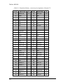
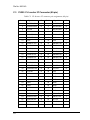
Table 2-3 Printer port LED boot mode status (2/5)
LED Status
Test item
05h
Message
PIT initialization
Start resume sequence
Resume error process
SM-RAM initialization
ROM to RAM copy and enabling shadow RAM
Toshiba register initialization (3)
06h
SMI initialization
SM-RAM base rewrite
KBC initialization (2)
Set SMI handler
Grant SMI
Estimate operation clock speed
Grant all SMIs
Measure for miscellaneous GA
Date check for alarm power on
Canceling HDD hardware reset
Set COMS default configuration when CMOS error
detected
KBC initialization
03h
04h
VGA initialization
VGA controller power off and reset control
Sound initialization
Sound controller initialization
PIT initialization
PIT test and initialization
PIC initialization
PIC initialization
PIC test
CPU type discrimination
Self-test control status initialization
02h
PCI initialization
PCI initialization
Detection of VGA controller on ISA
71h
Set CMOS initialize register
Printer port wraparound connector detection
CMOS data initialization for APM
Set divider control register
Set counter control register
Set configuration number and sleep counter
initialization
1-19
File No. 960-140
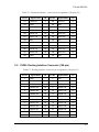
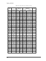
Table 2-3 Printer port LED boot mode status (3/5)
LED Status
Test item
Message
07h
PnP initialization
PnP initialization
73h
Desk station initialization
Initialization of NS Super I/O in desk station
72h
Get PnP information
PnP ISA card separation and get resource
information
74h
Password initialization
Password initialization
76h
TSETUP
TSETUP hardware configuration
Issuing power off grant command
Set CPU speed
Set speaker
Set battery alarm
Set panel close alarm
Set panel power on/off
PnP system resource configuration
79h
Serial port configuration
Serial port configuration
PC card configuration
Modem port configuration
PnP automatic configuration
PC card initialization
PnP automatic configuration
77h
EC and PSC configuration
Grant embedded controller SMI
SLP_TYP setting
Power supply microprocessor configuration
78h
PCI device initialization (1)
Ensure work area for automatic configuration
Initialization of work area
Create reserved resource map
81h
PCI device initialization (2)
Add reserved resource for primary display device to
map
82h
PCI device initialization (3)
Add reserved variable resource to map
83h
PCI device initialization (4)
PCI automatic configuration
Special process after PCI configuration
1-20
File No. 960-140
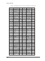
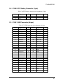
Table 2-3 Printer port LED boot mode status (4/5)
LED Status
7Bh
Test item
Message
HDD initialization
Printer port configuration
FDD initialization
HDD initialization
Serial interrupt control
FDD initialization
Open closing PCI device
7Ch
BIOS RAM update
IRQ routing table update
Copying parameter in IRT BIOS to runtime BIOS
7Ah
VGA initialization
Video card recognition and wait for VGA chip
initialization
08h
Output code generation
Output code generation
09h
First 64 KB memory check
First 64 KB memory check
0Dh
System configuration
Store CMOS error information to SM-RAM
Timer initialization
Get version of embedded controller and PS
microprocessor
Set default value to embedded controller
Toshiba special register initialization
Grant SMI from docking port and Selectable Bay
19h
Display initialization
VGA BIOS initialization
Selectable Bay lock check
Selectable Bay lock check
1Fh
Displaying logo
Displaying logo
20h
PnP configuration
PnP automatic configuration
PnP ISA card isolation
Search assignable resource and card configuration
21h
System memory check
System memory check
25h
Expansion memory check
Expansion memory check
30h
DMA page check
DMA page check
40h
DMAC check
DMAC check
41h
DMAC configuration
DMAC configuration
42h
Printer port check
Printer port check
70h
SIO check
SIO check
80h
NDP configuration
NDP configuration
1-21
File No. 960-140
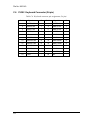
Table 2-3 Printer port LED boot mode status (5/5)
LED Status
Test item
Message
A0h
Boot password
Boot password
C0h
External I/O check
External I/O check
A6h
BIOS information update
Set font address
Set shadow RAM size
Set expansion memory size to CMOS
System resource update
Set extended memory size to runtime BIOS for
INT15h
ACPI table update
Set SCT area to runtime BIOS
Set battery save mode
Send date to PS microprocessor
Close PCI device configuration area
Protect system BIOS
Cache control
FEh
System ROM check
FFh
End
Check 1
System ROM check
If any of the following error codes display, go to Procedure 5.
B0h, B2h, B3h, 00h, 01h, 05h, 06h, 03h, 04h, 02h, 71h, 07h, 73h, 74h, 72h, 76h,
79h, 77h, 78h, 81h, 82h, 7Bh, 7Ch, 7Ah, 08h, 09h, 0Dh, 19h, 1Fh, 20h, 21h, 25h,
30h, 40h, 41h, 42h, 70h, 80h, A0h, C0h, A6h, FEh
Check 2
1-22
If error code 83h is displayed, go to the following sections:
Section 2.5. FDD Troubleshooting
Section 2.6. HDD Troubleshooting
File No. 960-140
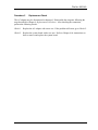
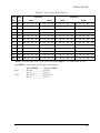
Procedure 3
Printer Port LED Check on Resume Mode
The printer port LED displays the IRT status and test status by turning lights on and off as an
eight-digit binary value for Hibernation mode.
To use the printer port LED follow the steps below:
1. Make sure the computer is in Resume mode.
2. Plug the printer port LED into the computer’s parallel port.
3. Turn on the computer’s power.
4. Read the LED status from left to right as you face the back of the computer.
5. Convert the status from binary to hexadecimal notation.
6. If the final LED status is FFh (normal status), go to Procedure 4.
7. If the final LED status matches any of the test status values in Table 2-4, perform
Procedure 5.
Table 2-4 Printer port LED Resume mode error status
Error status
Meaning of status
F1H
System BIOS RAM checksum error
F2H
External display card is connected.
F3H
HDD was installed.
F4H
SMRAM checksum error or memory error during suspend
F5H
Conventional memory checksum error
F7H
Extended memory checksum error
F8H
PnP RAM checksum error
1-23
File No. 960-140
Procedure 4
Diagnostic Test Program Execution Check
Execute the following tests from the Diagnostic Test Menu. Refer to Chapter 3,Tests and
Diagnostic, for more information on how to perform these tests.
1. System test
2. Memory test
3. Keyboard test
4. Display test
5. Floppy Disk test
6. Printer test
7. ASYNC test
8. Hard Disk test
9. Real Timer test
10. NDP test
11. Expansion test
12. Sound test
If an error is detected during these tests, go to Procedure 5.
Procedure 5
Replacement Check
The system board may be damaged. Disassemble the computer following the steps described
in Chapter 4, Replacement Procedures and replace the system board with a new one.
1-24
File No. 960-140
1.5
FDD Troubleshooting
This section describes how to determine if the FDD is functioning properly. Perform the steps
below starting with Procedure 1 and continuing with the other procedures as required.
Procedure 1: FDD Head Cleaning Check
Procedure 2: Diagnostic Test Program Execution Check
Procedure 3: Connector Check and Replacement Check
Procedure 1
FDD Head Cleaning Check
FDD head cleaning is one option available in the Diagnostic Program. A detailed operation is
given in Chapter 3, Tests and Diagnostics.
Insert the Diagnostics Disk in the computer’s floppy disk drive, turn on the computer and run
the test. Clean the FDD heads using the cleaning kit. If the FDD still does not function
properly after cleaning, go to Procedure 2.
If the test program cannot be executed on the computer, go to Procedure 2.
1-25
File No. 960-140
Procedure 2
Diagnostic Test Program Execution Check
Insert the Diagnostics Disk in the FDD, turn on the computer and run the test. Refer to
Chapter 3, Tests and Diagnostics, for more information about the diagnostics test procedures.
Floppy disk drive test error codes and their status names are listed in Table 2-5. Make sure the
floppy disk is formatted correctly and that the write protect tab is disabled. If any other errors
occur while executing the FDD diagnostics test, go to Check 1.
Table 2-5 FDD error code and status
Code
Check 1
Status
01h
Bad command
02h
Address mark not found
03h
Write protected
04h
Record not found
06h
Media removed on dual attach card
08h
DMA overrun error
09h
DMA boundary error
10h
CRC error
20h
FDC error
40h
Seek error
60h
FDD not drive
80h
Time out error (Not ready)
EEh
Write buffer error
FFh
Data compare error
If the following message displays, disable the write protect tab on the floppy disk.
If any other message appears, perform Check 2.
Write protected
Check 2
1-26
Make sure the floppy disk is formatted correctly. If it is, go to Procedure 3.
File No. 960-140
Procedure 3
Connector Check and Replacement Check
The FDD, cable and PC card is a single unit. Install the FDD's PC card in the computer, then
begin with Check 1 below.
Check 1
Make sure the PC card is properly connected to the system board.
If the connection is loose, reinstall the PC card and repeat Procedure 2. If there is
still an error, go to Check 2.
Check 2
The FDD may be defective or damaged. Replace the FDD with a new one. If the
FDD is still not functioning properly, perform Check 3.
Check 3
Replace the system board with a new one following the steps in Chapter 4,
Replacement Procedures.
1-27
File No. 960-140
1.6
HDD Troubleshooting
This section describes how to determine if the HDD is functioning properly. Perform the steps
below starting with Procedure 1 and continuing with the other procedures as required.
Procedure 1: Message Check
Procedure 2: Partition Check
Procedure 3: Format Check
Procedure 4: Diagnostic Test Program Execution Check
Procedure 5: Connector Check and Replacement Check
NOTE: The contents of the hard disk will be erased when the HDD troubleshooting
procedures are executed. Transfer the contents of the hard disk to floppy disk or other
device. If the customer has not or cannot perform the backup, create backup disks as
described below.
Check to see if the Microsoft Create System Disks Tools (MSCSD.EXE) still exists
in the System Tools Folder. (This tool can be used only once.) If it exists, use it to
back up the preinstalled software, then use the Backup utility in the System Tools
folder to back up the entire disk, including the user's files.
Refer to the operating system instructions.
1-28
File No. 960-140
Procedure 1
Message Check
When the computer’s HDD does not function properly, some of the following error messages
may appear on the display. Start with Check 1 below and perform the other checks as
instructed.
Check 1
If any of the following messages appear, go to Procedure 5. If the following
messages do not appear, perform Check 2.
HDC ERROR (After 5 seconds this message will disappear.)
or
HDD #0 ERROR (After 5 seconds this message will disappear.)
or
HDD #1 ERROR (After 5 seconds this message will disappear.)
Check 2
If either of the following messages appears, go to Procedure 2. If the following
messages do not appear, perform Check 3.
Insert system disk in drive
Press any key when ready .....
or
Non-System disk or disk error
Replace and press any key
Check 3
Check TSETUP to see whether the Hard Disk option is set to Not used. If it is set
to Not used, choose another setting and restart the computer. If the problem still
exists, go to Procedure 2.
1-29
File No. 960-140
Procedure 2
Partition Check
Insert the Toshiba MS-DOS system disk and restart the computer. Perform the following
checks:
Check 1
Type C: and press Enter. If you cannot change to drive C, go to Check 2. If you
can change to drive C, go to Check 3.
Check 2
Type FDISK and press Enter. Choose Display Partition Information from the
FDISK menu. If drive C is listed, go to Check 3. If drive C is not listed, return to
the FDISK menu and choose the option to create a DOS partition on drive C.
Restart the computer from the Toshiba MS-DOS system disk. If the problem still
exists, go to Procedure 3.
Check 3
If drive C is listed as active in the FDISK menu, go to Check 4. If drive C is not
listed as active, return to the FDISK menu and choose the option to set the active
partition for drive C. Restart the computer. If the problem still exists, go to Check
4.
Check 4
Type DIR C: and press Enter. If the following message displays, go to Procedure
3. If contents of drive C are listed on the display, go to Check 5.
Invalid media type reading drive C
Abort, Retry, Fail?
Check 5
Using the SYS command on the Toshiba MS-DOS system disk, install system files
on the HDD.
If the following message appears on the display, the system files have been
transferred to the HDD. Restart the computer. If the problem still exists, go to
Procedure 3.
System transferred
1-30
File No. 960-140
Procedure 3
Format Check
The computer’s HDD is formatted using the low level format program and the MS-DOS
FORMAT program. To format the HDD, start with Check 1 below and perform the other
steps as required.
Check 1
Format the HDD and transfer system files using FORMAT C:/S/U. If the
following message appears on the display, the HDD is formatted.
Format complete
If an error message appears on the display, refer to the Toshiba MS-DOS Manual
for more information and perform Check 2.
Check 2
Using the Diagnostic Disk, format the HDD with a low level format option. Refer
to Chapter 3, Tests and Diagnostics for more information about the diagnostic
program.
If the following message appears on the display, the HDD low level format is
complete. Partition and format the HDD using the MS-DOS FORMAT command.
Format complete
If you cannot format the HDD using the Tests and Diagnostic program, go to
Procedure 4.
1-31
File No. 960-140
Procedure 4
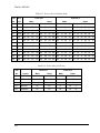
Diagnostic Test Program Execution Check
The HDD test program is stored in the Diagnostics Disk. Perform all of the HDD tests in the
Hard Disk Drive Test. Refer to Chapter 3, Tests and Diagnostics, for more information about
the HDD test program.
If an error is detected during the HDD test, an error code and status will display. The error
codes and statuses are listed in Table 2-6. If an error code is not generated and the problem
still exists, go to Procedure 5.
Table 2-6 Hard disk drive error code and status
Code
1-32
Status
01h
Bad command
02h
Bad address mark
04h
Record not found
05h
HDC not reset
07h
Drive not initialized
08h
HDC overrun (DRQ)
09h
DMA boundary error
0Ah
Bad sector error
0Bh
Bad track error
10h
ECC error
11h
ECC recover enable
20h
HDC error
40h
Seek error
80h
Time out error
AAh
Drive not ready
BBh
Undefined error
CCh
Write fault
E0h
Status error
EEh
Access time out error
DAh
No HDD
File No. 960-140
Procedure 5
Connector Check and Replaceme nt Check
The HDD or system board may be disconnected or damaged. Disassemble the computer
following the steps described in Chapter 4, Replacement Procedures and perform the
following checks:
Check 1
Make sure the HDD is firmly connected to system board.
If any of the connections are loose, reconnect firmly and repeat Procedure 1. If
there is still an error, go to Check 2.
Check 2
The HDD may be damaged. Replace it with a new one following the instructions in
Chapter 4. If the problem still exists, perform Check 3.
Check 3
The system board may be damaged. Replace it with a new one following the
instructions in Chapter 4.
1-33
File No. 960-140
1.7
Keyboard Troubleshooting
To determine if the computer’s keyboard is functioning properly, perform the following
procedures. Start with Procedure 1 and continue with the other procedures as instructed.
Procedure 1: Diagnostic Test Program Execution Check
Procedure 2: Connector and Replacement Check
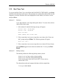
Procedure 1
Diagnostic Test Program Execution Check
Execute the Keyboard Test in the Diagnostic Program. Refer to Chapter 3, Test and
Diagnostics, for more information on how to perform the test program
If an error occurs, go to Procedure 2. If an error does not occur, the keyboard is functioning
properly
If the external keyboard appears to have the same problem as the internal keyboard, the
system board may be damaged. Go to Procedure 2.
1-34
File No. 960-140
Procedure 2
Connector and Replacement Check
The keyboard is connected to the system board by flat cables. These cables or connectors
may be disconnected or damaged. If there is a problem with the keyboard, disassemble the
computer as described in Chapter 4, Replacement Procedures, and perform Check 1.
Check 1
Make sure the following cables are not damaged and are connected to the system
board.
If the cables are damaged, replace the keyboard with a new one. If the cable is
disconnected, firmly connect it. Perform Procedure 1 again. If the error still
exists, perform Check 2.
Check 2
The system board may be damaged. Replace the system board with a new one.
Refer to Chapter 4, Replacement Procedures for more information.
1-35
File No. 960-140
1.8
Pointing Device Troubleshooting
To determine if the computer's pointing device is functioning properly, perform the following
procedures.
Procedure 1: Diagnostic Test Program Execution Check
Procedure 2: Connector and Replacement Check
Procedure 1
Diagnostic Test Program Execution Check
Execute the pointing device Test in the Diagnostic Program of Keyboard Test Program.
Refer to Chapter 3, Test and Diagnostic, for more information on how to perform the test
program. If an error occurs, go to Procedure 2. If an error does not occur, the pointing
device is functioning properly.
Procedure 2
Connector and Replacement Check
The pointing device is connected to the system board by the FLIMC* board (flexible cable).
The FLIMC* board or connectors may be disconnected or damaged. If there is a problem
with the pointing device, disassemble the computer as described in Chapter 4.Replacement
Procedures, and perform Check 1.
Check 1
Make sure the FLIMC* board or the pointing device is not damaged and that both
are connected to the system board. If the FLIMC* board or the pointing device is
damaged, replace the FLIMC* board or the pointing device with a new one. If the
FLIMC* board or the pointing device is disconnected, firmly connect it. Perform
Procedure 1 again. If the error still exists, perform Check 2.
Check 2
The System board may be damaged. Replace the System board with a new one.
Refer to Chapter 4, Replacement Procedures for more information.
1-36
File No. 960-140
1.9
Display Troubleshooting
This section describes how to determine if the computer’s display is functioning properly.
Start with Procedure 1 and continue with the other procedures as instructed.
Procedure 1: Diagnostic Test Program Execution Check
Procedure 2: Connector and Replacement Check
Procedure 1
Diagnostic Test Program Executi on Check
The Display Test program is stored on the computer’s Diagnostics disk. This program checks
the display controller on the system board. Insert the Diagnostics disk in the computer’s
floppy disk drive, turn on the computer and run the test. Refer to Chapter 3, Tests and
Diagnostics for details.
If an error is detected, go to Procedure 2. If an error is not detected, the display is functioning
properly.
1-37
File No. 960-140
Procedure 2
Connector and Replacement Check
The FL, FL inverter board, LCD module, LCD flat cable and system board are connected to
the display circuits. Any of these components may be damaged. Refer to Chapter 4,
Replacement Procedures, for instructions on how to disassemble the computer and then
perform the following checks:
If the FL does not light, perform Check 4.
If characters are not displayed clearly, perform Check 3.
If some screen functions do not operate properly, perform Check 3.
If the FL remains lit when the display is closed, perform Check4.
Check 1
Replace the LCD flat cable with a new one and test the display again. If the
problem still exists, perform Check 2.
Check 2
Replace the LCD module with a new one and test the display again. If the problem
still exists, perform Check 3..
Check 3
Replace the FL inverter board with a new one and test the display again. If the
problem still exists, perform Check 4.
Check 4
Replace the FL with a new one and test the display again. If the problem still
exists, perform Check 5.
Check 5
The system board may be damaged. Replace the system board with a new one.
1-38
File No. 960-140
Chapter 3
Tests and Diagnostics
File No. 960-140
3-ii
File No. 960-140
Chapter 3
Contents
3.1
The Diagnostic Test................................................................................................3-1
3.2
Executing the Diagnostic Test.................................................................................3-3
3.3
Subtest Names........................................................................................................3-7
3.4
System Test............................................................................................................3-9
3.5
Memory Test ........................................................................................................3-10
3.6
Keyboard Test ......................................................................................................3-12
3.7
Display Test..........................................................................................................3-16
3.8
Floppy Disk Test ..................................................................................................3-20
3.9
Printer Test...........................................................................................................3-22
3.10
Async Test............................................................................................................3-24
3.11
Hard Disk Test .....................................................................................................3-26
3.12
Real Timer Test....................................................................................................3-30
3.13
NDP Test .............................................................................................................3-32
3.14
Expansion Test .....................................................................................................3-33
3.15
Sound Test ...........................................................................................................3-35
3.16
Error Code and Error Status Names......................................................................3-36
3.17
Hard Disk Test Detail Status.................................................................................3-39
3.18
Hard Disk Format.................................................................................................3-41
3.19
3.20
3.21
3.18.1
Function Description........................................................................3-42
3.18.2
Operations .......................................................................................3-43
Head Cleaning ......................................................................................................3-46
3.19.1
Function Description........................................................................3-46
3.19.2
Operations .......................................................................................3-46
Log Utilities..........................................................................................................3-47
3.20.1
Function Description........................................................................3-47
3.20.2
Operations .......................................................................................3-47
Running Test ........................................................................................................3-49
3.21.1
Function Description........................................................................3-49
3.21.2
Operations .......................................................................................3-49
3-iii
File No. 960-140
3.22
3.23
3.24
Floppy Disk Drive Utilities....................................................................................3-51
3.22.1
Function Description........................................................................3-51
3.22.2
Operations .......................................................................................3-52
System Configuration............................................................................................3-56
3.23.1
Function Description........................................................................3-56
3.23.2
Operations .......................................................................................3-57
SETUP.................................................................................................................3-58
3.24.1
Function Description........................................................................3-58
3.24.2
Accessing the SETUP Program........................................................3-59
Tables
Table 3-1 Subtest names ....................................................................................................3-7
Table 3-2 Error codes and error status names ..................................................................3-36
Table 3-3 Hard disk controller status register contents......................................................3-39
Table 3-4 Error register contents......................................................................................3-40
Table 3-5 Hard disk formatting sequence..........................................................................3-42
3-iv
File No. 960-140
3
3.1
The Diagnostic Test
This chapter explains how to use the Diagnostic Test program to test the functions of the
computer’s hardware modules. The Diagnostics Program is stored on the Diagnostic Disk.
The Diagnostic Test consists of 12 programs that are grouped into the Service Program
Module (DIAGNOSTIC TEST MENU).
NOTES: To start the diagnostics, follow these steps:
1. Check all cables for loose connections.
2. Exit any application you may be using and close Windows.
The DIAGNOSTIC MENU consists of the following functions:
DIAGNOSTIC TEST
HARD DISK FORMAT
HEAD CLEANING
LOG UTILITIES
RUNNING TEST
FDD UTILITIES
SYSTEM CONFIGURATION
EXIT TO MS-DOS
SETUP
The DIAGNOSTIC TEST MENU contains the following functional tests:
SYSTEM TEST
MEMORY TEST
KEYBOARD TEST
DISPLAY TEST
FLOPPY DISK TEST
PRINTER TEST
ASYNC TEST
HARD DISK TEST
REAL TIMER TEST
NDP TEST
EXPANSION TEST
SOUND TEST
3-1
File No. 960-140
You will need the following equipment to perform some of the Diagnostic test programs.
The Diagnostics Disk (all tests)
A formatted working disk for the floppy disk drive test (all tests)
A cleaning kit to clean the floppy disk drive heads (Head Cleaning)
A PC card wraparound connector for the I/O card test (Expansion test) (Rev.B or
higher)
A printer wraparound connector for the printer wraparound test (Printer test)
External FDD (All tests)
Serial port wraparound connector (ASYNC test)
I/O Adapter
The following sections detail the tests within the Diagnostic Test function of the
DIAGNOSTIC TEST MENU. Refer to Sections 3.18 through 3.24 for detailed information
on the remaining Service Program Module functions.
3-2
File No. 960-140
3.2
Executing the Diagnostic Test
Toshiba MS-DOS is required to run the DIAGNOSTICS PROGRAM. To start the
DIAGNOSTIC PROGRAM, follow these steps:
1. Connect a wraparound connector to the I/O adapter's printer port and RS-232C port.
Connect the I/O adapter to the computer. Next, connect the FDD and insert the
diskette containing the test program
2. Turn on the computer and the test program will execute and the test menu will be
displayed.
The following menu will appear:
TOSHIBA personal computer
xxx DIAGNOSTICS
version X.XX (c) copyright TOSHIBA Corp. 19XX
DIAGNOSTICS
1
2
3
4
5
6
7
8
9
0
-
MENU :
DIAGNOSTIC TEST
HARD DISK FORMAT
HEAD CLEANING
LOG UTILITIES
RUNNING TEST
FDD UTILITIES
SYSTEM CONFIGURATION
EXIT TO MS-DOS
SETUP
NOTE: To exit the DIAGNOSTIC TEST MENU, press the Esc key. If a test program is in
progress, press Ctrl + Break to exit the test program, or press Ctrl + C to stop the test
program.
3-3
File No. 960-140
3. To select the DIAGNOSTIC TEST option from the DIAGNOSTICS MENU, set the
highlight bar to 1 and press Enter. The following DIAGNOSTIC TEST MENU will
appear:
TOSHIBA personal computer
xxx DIAGNOSTICS
version X.XX (c) copyright TOSHIBA Corp. 19XX
DIAGNOSTIC TEST MENU :
1
2
3
4
5
6
7
8
9
10
11
12
88
99
–
-
SYSTEM TEST
MEMORY TEST
KEYBOARD TEST
DISPLAY TEST
FLOPPY DISK TEST
PRINTER TEST
ASYNC TEST
HARD DISK TEST
REAL TIMER TEST
NDP TEST
EXPANSION TEST
SOUND TEST
ERROR RETRY COUNT SET [HDD & FDD]
EXIT TO DIAGNOSTICS MENU
Refer to sections 3.4 through 3.16 for detailed descriptions of each Diagnostic Test 1 through
12. Function 88 sets the floppy disk drive and hard disk drive error retry count. Function 99
exits the submenus of the Diagnostic Test and returns to the Diagnostic Menu.
3-4
File No. 960-140
4. Select the option you want to execute and press Enter. The following message
appears:
SYSTEM TEST
XXXXXXX
SUB- TEST : XX
PASS COUNT: XXXXX
WRITE DATA: XX
ADDRESS : XXXXXX
xxx DIAGNOSTIC TEST VX.XX
[Ctrl]+[Break] ; test end
[Ctrl]+[C] ; key stop
ERROR COUN T: XXXXX
READ DATA : XX
STATUS : XXX
SUB-TEST MENU :
01
02
03
04
05
06
07
08
99
-
ROM checksum
Thermister check
Quick charge
DMI read
DMI write
Exit to DIAGNOSTIC TEST MENU
NOTE: The menu displayed by your computer may be slightly different from the
one shown above.
5. Select the desired subtest number from the subtest menu and press Enter. The
following message will appear:
TEST LOOP : YES
ERROR STOP : YES
Use the arrow keys to move the cursor to the desired option and press Enter.
Selecting YES for TEST LOOP sets the test to run continuously until halted by the
user. Selecting NO returns the subtest menu to the main menu after the test is
complete.
3-5
File No. 960-140
Selecting YES for ERROR STOP stops the test program when an error is found and
displays the operation guide on the right side of the display screen as shown below:
ERROR STATUS NAME
[ [ HALT OPERATION ]]
1: Test end
2: Continue
3: Retry
These three selections have the following functions respectively:
1. Terminates the test program and exits to the subtest menu.
2. Continues the test.
3. Restarts the test from the error.
Selecting NO for ERROR STOP keeps the test running even if an error is found.
Table 3-1 in Section 3.3 lists the function of each test on the subtest menu. Table 3-2 in
Section 3.16 lists the error codes and error status for each error.
3-6
File No. 960-140
3.3
Subtest Names
Table 3-1 lists the subtest names for each test program in the DIAGNOSTIC TEST MENU.
Table 3-1 Subtest names (1/2)
No.
Test Name
Subtest No.
Subtest Name
1
SYSTEM
01
05
06
07
08
ROM checksum
Thermistor check
Quick charge
DMI read (Not used)
DMI write (Not used)
2
MEMORY
01
02
03
04
05
06
RAM constant data
RAM address pattern data
RAM refresh
Protected mode
Memory module
Cache memory
3
KEYBOARD
01
02
03
04
05
Pressed key display
Pressed key code display
PS/2 Mouse connect check
Pointing Stick
USB Warp around test
4
DISPLAY
01
02
03
04
05
VRAM read/write for VGA
Gradation for VGA
Gradation & Mode test for VGA
“H” pattern display
BUS Master Transfaer
5
FDD
01
02
03
04
05
Sequential read
Sequential read/write
Random address/data
Write specified address
Read specified address
6
PRINTER
01
02
03
Ripple pattern
Function
Wraparound
3-7
File No. 960-140
Table 3-1 Subtest names (2/2)
No.
3-8
Test Name
Subtest No.
Subtest Name
7
ASYNC
01
02
03
04
06
07
Wrap around (board)
Point to point (send)
Point to point (receive)
Interrupt test
FIR/SIR point to point (send)
FIR/SIR point to point (receive)
8
HDD
01
02
03
04
05
06
07
08
09
10
Sequential read
Address uniqueness
Random address/data
Cross talk & peak shift
Write/read/compare (CE)
Write specified address
Read specified address
ECC circuit
Sequential write
W-R-C specified address
9
REAL TIMER
01
02
03
Real time
Backup memory
Real time carry
10
NDP
01
NDP test
11
EXPANSION
01
02
03
04
06
PCMCIA wrap around
DS bus wrap around
RGB monitor ID
PCMCIA wrap around (External)
ZV port wrap around
12
SOUND
01
02
03
CODEC (REC/PLAY)
FM Synthesizer
SIN Wave Playback
File No. 960-140
3.4
System Test
To execute the System Test select 1 from the DIAGNOSTIC TEST MENU, press Enter and
follow the directions on the screen. Move the highlight bar to the subtest you want to execute
and press Enter.
Subtest 01
ROM Checksum
This subtest executes a checksum test of the BIOS ROM on the system board.
Subtest 05
Thermistor Check
This subtest reads the thermistor connect check status of the power supply
microprocessor, then compares it with the original data. If the data indicates
the connector is open or shorted, it displays an error message.
Subtest 06
Quick Charge
This subtest determines whether the battery pack can be quick charged. Refer
to the table listing the result codes in Chapter 2.
3-9
File No. 960-140
3.5
Memory Test
To execute the Memory Test, select 2 from the DIAGNOSTIC TEST MENU, press Enter
and follow the directions on the screen. Move the highlight bar to the subtest you want to
execute and press Enter.
Subtest 01
RAM constant data (real mode)
This subtest writes a 256-byte unit of constant data to conventional memory (0
to 640 KB). Then reads the new data and compares the result with the original
data. The constant data is FFFFh, AAAAh, 5555h, 0101h, and 0000h.
Subtest 02
RAM address pattern data (real mode)
This subtest writes address pattern data created by the exclusive-ORing
(XORing), to the address segment and address offset in conventional memory
program end to 640 KB, then reads the new data and compares the result with
the original data.
Subtest 03
RAM refresh (real mode)
This subtest writes a 256-byte unit of constant data to conventional memory (0
to 640 KB) then reads the new data and compares the result with the original
data.
The constant data is AAAAh and 5555h.
NOTE: There is a short delay between write and read operations,
depending on the size of the data.
Subtest 04
Protected mode
NOTE: The CONFIG.SYS file must be configured without expanded
memory manager programs such as EMM386.EXE, EMM386.SYS or
QEMM386.SYS. Also, the HIMEM.SYS must be deleted from the
CONFIG.SYS file.
This subtest writes constant data and address data to extended memory
(maximum address 100000h) then reads the new data and compares the result
with the original data.
The constant data is FFh, AAh, 55h, and 00h.
3-10
File No. 960-140
Subtest 05
Memory module
NOTE: To execute this subtest, an optional memory card must be
installed in the computer.
This subtest functions the same as subtest 04, except it is used for testing an
optional memory card. Memory module capacity is 32MB.
After selecting subtest 05, the following message will appear:
Extended memory size (1:32 MB)?
Select the number that corresponds to the memory card installed in the
computer.
Subtest 06
Cache memory
To test the cache memory, a pass-through write-read comparison of ‘5A’ data
is run repeatedly to the test area (‘7000’:’Program’ size to ‘7000’:’7FFF’ (32
KB)) to check the hit-miss ratio (on/off status) for CPU cache memory. One
test takes 3 seconds.
Number of misses < Number of hits → OK
Number of misses ≥ Number of hits → Fail
3-11
File No. 960-140
3.6
Keyboard Test
To execute the Keyboard Test, select 3 from the DIAGNOSTIC TEST MENU, press Enter
and follow the directions on the screen. The Keyboard test contains four subtests that test the
computer’s keyboard, PS/2 mouse, and Pointing Stick actions. Move the highlight bar to the
subtest you want to execute and press Enter.
Subtest 01
Pressed key display (80/82)
NOTE: The Num Lock and the Overlay mode must be off to execute
this subtest.
When you execute this subtest, the keyboard layout is drawn on the display as
shown below. When any key is pressed, the corresponding key on the screen
changes to the key that was pressed. Holding a key down enables the autorepeat function which causes the key’s display character to blink.
[[[
Press Key Display
]]]
If test OK, Press [Del] [Enter] Key
3-12
File No. 960-140
Subtest 02
Pressed key code display
When a key is pressed, the scan code, character code, and key top name
displays on the screen in the format shown below. The Ins, Caps Lock,
Num Lock, Scroll Lock, Alt, Ctrl, Left Shift, and Right Shift keys
display in reverse screen mode when pressed. The scan codes, character codes,
and key top names are shown in Appendix D.
KEYBOARD TEST
IN PROGRESS
Scan code =
Character code
Keytop
=
302000
=
Ins Caps Lock
Num Lock Scroll Lock
Alt Ctrl Left Shift Right Shift
PRESS [Enter] KEY
Subtest 03
PS/2 Mouse connect check
NOTE: To execute the PS/2 mouse connect check, a PS/2 mouse must be
connected to the computer before the power is turned on.
This subtest checks whether a PS/2 mouse is connected or not.
If this test does not detect an error, it returns to the subtest menu. If it detects
an error, the following message appears:
KBD - MOUSE INTERFACE ERROR
[[ HALT OPERATION ]]
1: Test end
2: Continue
3: Retry
3-13
File No. 960-140
Subtest 04
Pointing stick
This subtest checks the functions of the pointing stick as shown below.
A) IPS stick pressure sensing direction and parameter.
B) IPS switch function check.
This test reports the pointing stick motion response from the IPS and IPS
switch. When the stick is pressed towards the upper left, the <POINTING>
display changes according to the following illustration. If an IPS switch is
pressed, the <BUTTON> display alternates between black and white. The
parameters appear on the right side of the display. If two IPS switches are
pressed at the same time, the subtest menu displays.
3-14
File No. 960-140
Subtest 05
USB Wrap around test
This subtest checks USB. The USB TEST Module (ZD0003P01) and USB
Cable (ZD0003P02) must be connected to the computer.
If the test is completed successfully, OK is displayed. If nothing is displayed,
there may be a problem with the USB port. Check the wraparound connection
and repeat the test.
NOTE: To execute this subtest, the Enhanced Port Replicator must be
connected to the computer.
3-15
File No. 960-140
3.7
Display Test
To execute the Display Test, select 4 from the DIAGNOSTIC TEST MENU, press Enter and
follow the directions on the screen. The Display test contains eight subtests that test the
display in various modes. Move the highlight bar to the subtest you want to execute and press
Enter.
Subtest 01
VRAM read/write for VGA
This subtest writes constant data AAh and 55h and address data to video RAM
(2MB: A0000h-AFFFFh). This data is then read from the video RAM and
compared to the original data.
Subtest 02
Gradation for VGA
This subtest displays four colors: red, green, blue and white from left to right
across the screen from black to maximum brightness. The display below
appears on the screen when this subtest is executed.
To exit this subtest and return to the DISPLAY TEST menu, press Ctrl +
Break.
3-16
File No. 960-140
Subtest 03
Gradation & mode test for VGA
This subtest displays gradations for each mode. Execute the test, then press
Enter to change the mode.
Resolution
Mode
800 x 480
3, 12, 13
NOTE: Mode 52 test can test only an external monitor, it cannot be used
for the internal LCD.
The display below appears on the screen when this subtest is executed.
Pressing Enter changes the size of the displayed image.
Pressing Enter changes the size of the displayed image.
3-17
File No. 960-140
Pressing Enter again changes the size of the displayed image.
To exit this subtest and return to the DISPLAY TEST menu, press Ctrl +
Break.
3-18
File No. 960-140
Subtest 04
“H” pattern display
This subtest displays a full screen of “H” patterns.
HHHHHHHHHHHHHHHHHHHHHHHHHHHHHHHHHHHHHHHHHHHHHHHHHH
HHHHHHHHHHHHHHHHHHHHHHHHHHHHHHHHHHHHHHHHHHHHHHHHHH
HHHHHHHHHHHHHHHHHHHHHHHHHHHHHHHHHHHHHHHHHHHHHHHHHH
HHHHHHHHHHHHHHHHHHHHHHHHHHHHHHHHHHHHHHHHHHHHHHHHHH
HHHHHHHHHHHHHHHHHHHHHHHHHHHHHHHHHHHHHHHHHHHHHHHHHH
HHHHHHHHHHHHHHHHHHHHHHHHHHHHHHHHHHHHHHHHHHHHHHHHHH
HHHHHHHHHHHHHHHHHHHHHHHHHHHHHHHHHHHHHHHHHHHHHHHHHH
HHHHHHHHHHHHHHHHHHHHHHHHHHHHHHHHHHHHHHHHHHHHHHHHHH
HHHHHHHHHHHHHHHHHHHHHHHHHHHHHHHHHHHHHHHHHHHHHHHHHH
HHHHHHHHHHHHHHHHHHHHHHHHHHHHHHHHHHHHHHHHHHHHHHHHHH
HHHHHHHHHHHHHHHHHHHHHHHHHHHHHHHHHHHHHHHHHHHHHHHHHH
HHHHHHHHHHHHHHHHHHHHHHHHHHHHHHHHHHHHHHHHHHHHHHHHHH
HHHHHHHHHHHHHHHHHHHHHHHHHHHHHHHHHHHHHHHHHHHHHHHHHH
HHHHHHHHHHHHHHHHHHHHHHHHHHHHHHHHHHHHHHHHHHHHHHHHHH
HHHHHHHHHHHHHHHHHHHHHHHHHHHHHHHHHHHHHHHHHHHHHHHHHH
To exit this subtest and return to the DISPLAY TEST menu, press Ctrl +
Break.
NOTE: The last row may not be completely filled. This condition does not
indicate on error
Subtest 05
BUS Master Transfer
This subtest PCI BUS MASTER test.
3-19
File No. 960-140
3.8
Floppy Disk Test
NOTE: Before running the floppy disk test, prepare a formatted work disk. Remove the
Diagnostics Disk and insert the work disk into the FDD. The contents of the floppy disk
will be erased.
To execute the Floppy Disk Test, select 5 from the DIAGNOSTIC TEST MENU, press
Enter and follow the directions displayed on the screen. The Floppy Disk test contains five
subtests that test the FDD. The following messages will appear after selecting the Floppy Disk
Test from the DIAGNOSTIC TEST MENU. Answer each question with an appropriate
response to execute the test.
1. Select the test drive number of the floppy disk drive to be tested and press Enter.
Test drive number select (1:FDD#1,2:FDD#2,0:FDD1&2
) ?
2. Select the media type of the floppy disk in the test drive to be tested, and pressEnter.
Media in drive #X mode (0:2DD
,1:2D,2:2D-2HD/2DD,3:2HD) ?
3. Select the track you want the test to start on and press Enter.
Test start track (Enter
:0/dd:00-79) ?
4. The floppy disk test menu will appear after you select. Select the number of thesubtest
you want to execute and press Enter. The following message will appear during the
floppy disk test.
3-20
File No. 960-140
Subtest 01
Sequential read
This subtest performs a Cyclic Redundancy Check (CRC) that continuously
reads all the tracks on a floppy disk. The following tracks are read according to
the media type in the floppy disk drive:
Double-sided, double-density (2D): Tracks 0 to 39.
Double-sided, double-density, double-track (2DD) and doublesided, high-density, double-track (2HD): Tracks 0 to 79.
The start track is specified when the FDD test is started from the Diagnostic
Test Menu. Refer to Step 3 at the beginning of this section to set the start
track.
Subtest 02
Sequential read/write
This subtest continuously writes data pattern B5ADADh to all the specified
tracks selected in subtest 01. The data is then read and compared to the
original data.
Subtest 03
Random Address/Data
This subtest writes random data to random addresses on all tracks defined in
subtest 01. The data is then read and compared to the original data.
Subtest 04
Write Specified Address
This subtest writes specified data to a specified track, head, and address.
Subtest 05
Read Specified Address
This subtest reads data from a specified track, head, and address.
3-21
File No. 960-140
3.9
Printer Test
To execute the Printer Test, select 6 from the DIAGNOSTIC TEST MENU, press Enter and
follow the directions on the screen. The Printer Test contains three subtests that test the
output of the printer connected to the computer. The following messages will appear after
selecting the Printer Test. Answer each of the questions with an appropriate response to
execute the test.
NOTE: An IBM compatible printer must be connected to the system to execute this test.
The following message will appear when the printer test is selected:
channel#2 = XXXXh
channel#3 = XXXXh
Select the channel number (1-3
) ?
The printer I/O port address is specified by the XXXXh number. The computer supports three
printer channels. Select the printer channel number and press Enter to execute the selected
subtest.
Subtest 01
Ripple pattern
This subtest prints characters for codes 20h through 7Eh line-by-line while
shifting one character to the left at the beginning of each new line.
3-22
File No. 960-140
Subtest 02
Function
This subtest is for IBM compatible printers and tests the following functions:
Normal print
Double-width print
Compressed print
Emphasized print
Double-strike print
All characters print
This subtest prints the various print types shown below:
Subtest 03
Wraparound
NOTE: To execute this subtest, a parallel port wraparound connector
must be connected to the computer’s printer port. The connector’s
(34M741986G01) wiring diagram is shown in Appendix F.
This subtest checks the output and bi-directional modes of the data control and
status lines through the parallel port wraparound connector.
3-23
File No. 960-140
3.10
Async Test
To execute the Async Test, select 7 from the DIAGNOSTIC TEST MENU, press Enter and
follow the directions on the screen. The async test contains seven subtests that test the
asynchronous communication functions. Move the highlight bar to the subtest you want to
execute and press Enter.
The Subtests require the following data format:
Method:
Speed:
Asynchronous
9600BPS (Subtests 01 to 04)
38400BPS (Subtests 06, 07)
Data:
8 bits and one parity bit (EVEN)
Data pattern: 20h to 7Eh
The following message will appear at the bottom of the screen when subtests 01, 02, 03, 06,
and 07 are selected:
Channel#1 = XXXXh
Channel#2 = XXXXh
Channel#3 = XXXXh
Select the Channel number (1/2/3)
The serial I/O port address is specified by the XXXXh number. Select the serial port channel
number and press Enter to start the subtest.
Subtest 01
Wrap around (board)
NOTE: To execute this subtest an RS-232C wraparound connector
(34M741621G01) must be connected to the RS-232C port. The RS-232C
wraparound connector wiring diagram is described in Appendix F.
This subtest checks the data send/receive function through the wraparound
connector.
Subtest 02
Point to point (send)
NOTE: To execute this subtest, two machines must be connected with an
RS-232-C direct cable. One machine should be set as “send”(subtest 02)
and the other set as “receive” (subtest 03). The wiring diagram for the
RS-232-C direct cable is shown in Appendix F.
This subtest sends 20h through 7Eh data to the receive side, then receives the
sent data and compares it to the original data.
3-24
File No. 960-140
Subtest 03
Point to point (receive)
This subtest is used with subtest 02 described above. This subtest receives the
data from the send side, then sends the received data.
Subtest 04
Interrupt test
This subtest checks the Interrupt Request Level of IRQ 4, 3 and 5 from the
send side.
Subtest 06
FIR/SIR Point to point (send)
NOTE: To execute subtests 06 and 07, each computer must have access to
the other computer’s infrared port.
This subtest sends 20h through 7Eh data to the receive side, then receives the
sent data and compares it to the original data through the SIR port.
Subtest 07
FIR/SIR Point to point (receive)
This subtest is used with subtest 06 described above. This subtest receives the
data from the send side, then sends the received data through the SIR port.
NOTE: Select subtest numbers ,06 and 07.
The following message will appear:
Select the UIRCC mode (1:FIR /2:SIR)?
1: FIR mode
2: SIR mode
3-25
File No. 960-140
3.11
Hard Disk Test
To execute the Hard Disk Test, select 8 from the DIAGNOSTIC TEST MENU, press Enter,
and follow the directions on the screen. The hard disk test contains ten subtests that test the
hard disk drive functions.
NOTE: The contents of the hard disk will be erased when subtest 02, 03, 04, 05, 06, 08,
09, or 10 is executed. Before running the test, the customer should transfer the
contents of the hard disk to floppy disk. If the customer has not or cannot
perform the back-up, create back-up disks as described below.
Check to see if the Microsoft Create System Disks Tools (MSCSD.EXE) still
exists in the System Tools Folder. (This tool can be used only once.) If it exists,
use it to back up the pre-installed software, then use the Backup utility in the
System Tools folder to back up the entire disk, including the user’s files.
Refer to the operating system instructions.
The following messages will appear after selecting the hard disk test from the DIAGNOSTIC
TEST MENU. Answer each of the questions with an appropriate response to execute the test:
[HDD test parameters]
Test drive number
:#1
HDC F/W error retry
:yes
Data compare error dump
:no
Detail status display
:no
↑↓→←:Select
↑↓→←
items, Enter:Finish, Esc:Exit,F5:Set default
1. Select the hard disk drive number to be tested:
Test drive number
HDD#1
HDD#2
HDD1&2
2. This message is used to select the retry operation when the hard disk controller detects
an error. Select yes or no.
HDC F/W error retry
yes
no
3. This message is used to select the error dump operation when a data compare error is
detected. Select yes or no:
Data compare error dump
3-26
yes
no
File No. 960-140
4. This message is used to select whether or not the HDD status is displayed on the
screen. The HDD status is described in section 3.19. Select yes or no:
Detail status display
yes
no
5. This message is used to select whether or not the HDD status is displayed on the
screen. The HDD status is described in section 3.19. Select 1 or 2 and press Enter.
6. The Hard Disk Test message will appear after you respond to the Detail Status
prompt. Select the number of the subtest you want to execute and press Enter. The
following message will appear during each subtest.
HARD DISK
TEST
XXXXXXX
SUB- TEST : XX
PASS COUNT: XXXXX ERROR COUNT: XXXXX
WRITE DATA: XX READ DATA : XX
ADDRESS : XXXXXX STATUS : XXX
The first three digits of the ADDRESS indicate which cylinder is being tested, the
fourth digit indicates the head and the last two digits indicate the sector.
The first digit of the STATUS number indicates the drive being tested and the last two
digits indicate the error status code as explained in Table 3-2.
Subtest 01
Sequential read
This subtest is a sequential reading of all the tracks on the HDD starting at
track 0. When all the tracks on the HDD have been read, the test starts at the
maximum track and reads the tracks on the HDD sequentially back to track 0.
Subtest 02
Address uniqueness
This subtest writes unique address data to each sector of the HDD track-bytrack. The data written to each sector is then read and compared with the
original data. There are three ways the HDD can be read:
•
•
•
Subtest 03
Forward sequential
Reverse sequential
Random
Random address/data
This subtest writes random data to random addresses on the HDD cylinder,
head and sector. This data is then read and compared to the original data.
3-27
File No. 960-140
Subtest 04
Cross talk & peak shift
This subtest writes eight types of worst pattern data (listed below) to a
cylinder, then reads the data while moving from cylinder to cylinder.
Subtest 05
Worst pattern data
Cylinder
‘B5ADAD’
0 cylinder
‘4A5252’
1 cylinder
‘EB6DB6’
2 cylinder
‘149249’
3 cylinder
’63B63B’
4 cylinder
‘9C49C4’
5 cylinder
‘2DB6DB’
6 cylinder
‘D24924’
7 cylinder
Write/read/compare (CE)
This subtest writes B5ADADh worst pattern data to the CE cylinder on the
HDD, then reads the data from the CE cylinder and compares it with the
original data.
Subtest 06
Write specified address
This subtest writes specified data to a specified cylinder and head on the HDD.
Subtest 07
Read specified address
This subtest reads data which has been written to a specified cylinder and head
on the HDD.
Subtest 08
ECC circuit
This subtest checks the Error Check and Correction (ECC) circuit functions of
the specified cylinder and head on the HDD.
Subtest 09
Sequential write
This subtest writes specified 2-byte data to all of the cylinders on the HDD.
Subtest 10
W-R-C specified address
This subtest writes data to a specified cylinder and head on the HDD, then
reads the data and compares it to the original data.
3-28
File No. 960-140
3
3.12
Real Timer Test
To execute the Real Timer Test, select 9 from the DIAGNOSTIC TEST MENU, press Enter
and follow the directions on the screen. The real timer test contains three subtests that test the
computer’s real timer functions. Move the highlight bar to the subtest you want to execute
and press Enter.
Subtest 01
Real time
A new date and time can be input during this subtest. To execute the real time
subtest follow these steps:
1. Select subtest 01 and the following message will appear:
Current date : XX-XX-XXXX
Current time : XX:XX:XX
Enter new date:
PRESS [ENTER] KEY TO EXIT TEST
2. If the current date is not correct, input the correct date at the “Enter new
date” prompt and press Enter. The following prompt will appear:
Enter new
time :
3. If the current time is not correct, input the correct time in 24-hour format.
Pressing Enter toggles between the time and the date. To exit, press Ctrl +
Break.
Subtest 02
Backup memory
This subtest performs the following backup memory check:
Writes 1-bit of “on” data to address 01h through 80h
Writes 1-bit of “off” data to address 0Eh through 80h
Writes the data pattern AAh and 55h to the RTC 114-byte memory
(address 0Eh to 7Fh)
The subtest then reads and compares this data with the original data.
To exit, press Ctrl + Break.
3-29
File No. 960-140
Subtest 03
Real time carry
CAUTION: When this subtest is executed, the current date and time are erased.
This subtest checks the real time clock increments, making sure the date and
time are displayed in the following format:
Current date
Current time
:
:
12-31-19 95
23:59:58
Pressing Enter displays the following
Current date :
Current time :
01-01-1996
00:00:00
PRESS [Enter] KEY TO EXIT TEST
Press Ctrl + Break to exit.
3-30
File No. 960-140
3.13
NDP Test
To execute the NDP test, select 10 from the DIAGNOSTICS TEST MENU, press Enter and
follow the directions on the screen. The NDP test contains one subtest that tests the
computer’s NDP functions.
Subtest 01
NDP
This test checks the following functions of the coprocessor:
Control word
Status word
Bus
Addition
Multiplication
Press Ctrl + Break to exit.
3-31
File No. 960-140
3.14
Expansion Test
To execute the expansion test, select 11 from the DIAGNOSTICS TEST MENU, press
Enter and follow the directions on the screen.
NOTE:
Subtest 01
To execute this subtest, the PC card wraparound connector is required.
PCMCIA wrap around
This test checks the following signal line of the PC card slot:
Address line
REG#, CE#1, CE#2 line
Data line
Speaker line
Wait line
BSY#, BVD1 line
This subtest is executed in the following order:
Sub#
Address
Good
Bad
Contents
01
00001
00001
nn
nn
xx
xx
Address line
REG#, CE#1, CE#2
nn=A0, 90, 80, 00
02
00002
ww
rr
Data line
ww=write data, rr=read data
03
00003
––
––
Speaker line
04
00004
40,80
xx
Wait line (40<xx<80)
05
00005
nn
xx
Other lines (BSY#, BVD1)
NN=21, 00
NOTE: Select the subtest number01the following message will appear: Test slot number
select (1:slot0, 2:slot1, 0:slot0&1) ?
3-32
File No. 960-140
NOTE: Subtests 02 and 04 are for Enhanced Port Replicator . For procedures on those
subtests, refer to Enhanced Port Replicator manual.
Subtest 03
RGB monitor ID test
Connect a wrap around Board to the external monitor port to test the RGB
monitor ID.
Subtest 06
ZV Port wrap around
Use the PC Card/ZV Test Card (Rev.B or higher) to conduct the test. The
video and audio interfaces will be tested. When the video test is initiated, the
board automatically writes data AAAAh and 5555h alternately to address
A000:0000h. The data written first is determined randomly, and has no effect
on the validity of the test.
After the video test is run the audio interface is tested. The test emits 1kHz
sine wave sound on the left speaker and 2kHz sine wave sound on the right
speaker.
3-33
File No. 960-140
3.15
Sound Test
To execute the sound test, select 12 from the DIAGNOSTICS TEST MENU, press Enter
and follow the directions on the screen. The sound test contains four subtests that test the
computer’s sound functions.
NOTE: To execute this subtest, the internal microphone and internal headphone (or
internal speaker) are required. The system is capable of producing high volume sound, so
when you use the headphones be careful to set the volume low and adjust it as necessary.
Using the headphones at full volume could damage your ears.
Subtest 01
CODEC (REC/PLAY)
Test the functions of the Codec (AD1848) A/D, D/A converter. Test the
microphone terminals and headphone terminals at the same time. When you
execute this subtest the following message displays.
[Quick REC & PLAY for AD1848]
Press any key to *** REC ***
After pressing any key, start recording and immediately play the sound. (It
takes three seconds.)
Subtest 02
FM Synthesizer
Test the OPL3 (YMF262) functions. Connect the headphone and check the
scale on the right and left sides. Also check the sound adjustment volume.
Subtest 03
SIN Wave Playback
This subtest expands the sine wave data table to 64KB and creates sine wave
data. The play data is transferred between DMA and CODEC, and plays the
sound. (It is a long beep.) Also, using the oscilloscope, observe the sine
waveform.
3-34
File No. 960-140
3.16
Error Code and Error Status Names
Table 3-2 lists the error codes and error status names for the Diagnostic Test.
Table 3-2 Error codes and error status names (1/3)
Device name
Error code
Error status name
(Common)
FF
Data Compare Error
System
01
02
03
ROM Checksum Error
Location ID error
Serial ID Write error
Memory
01
02
14
DD
DE
DF
Parity Error
Protected Mode Not Changed
Memory Read/Write Error
Cache Memory Error
2nd Cache Error
TAG-RAM Error
FDD
01
02
03
04
06
08
09
10
20
40
60
80
EE
FF
Bad Command
Address Mark Not Found
Write Protected
Record Not Found
Media Removed
DMA Overrun Error
DMA Boundary Error
CRC Error
FDC Error
Seek Error
Not Drive Error
Time Out Error
Write Buffer Error
Data Compare Error
Keyboard
01
02
03
04
05
06
Mouse interface error
IPS interface error
Interface error
Retransmi error
Mouse handler not support
PS/2 mouse & IPS not support
Printer
01
08
10
20
40
80
Time Out
Fault
Select Line
Out Of Paper
Power Off
Busy Line
3-35
File No. 960-140
Table 3-2 Error codes and error status names (2/3)
Device name
3-36
Error code
Error status name
ASYNC
01
02
04
08
10
20
40
50
60
70
80
88
[DSR On] Time Out
[CTS On] Time Out
[RX READY] Time Out
[TX FULL] Time Out
Parity Error
Framing Error
Overrun Error
Underrun error
Timer time out error
CRC error
Line Status Error
Modem Status Error
HDD
01
02
04
05
07
08
09
0A
0B
10
11
20
40
80
AA
BB
CC
EO
EE
DA
Bad Command Error
Address Mark Not Found
Record Not Found
HDC Not Reset Error
Drive Not Initialized
HDC Overrun (DRQ)
DMA Boundary Error
Bad Sector
Bad Track Error
ECC Error
ECC Recover Enable
HDC Error
Seek Error
Time Out Error
Drive Not Ready
Undefined Error
Write Fault
Status Error
Access Time Out Error
No HDD
Expansion
C1
C2
C3
C4
C5
C6
C7
C8
CB
CD
ADDRESS Line error
REG# Line error
CE#1 Line error
CE#2 Line error
DATA Line error
WAIT Line error
BSY# Line error
BVD1 Line error
ZV Port error
No PCMCIA
NDP
01
02
03
04
05
06
No Co-Processor
Control Word Error
Status Word Error
Bus Error
Addition Error
Multiply Error
File No. 960-140
Table 3-2 Error codes and error status names (3/3)
Device name
PCMCIA
Error code
C1
C2
C3
C4
C5
C6
C7
C8
CB
CD
Error status name
Address Line Error
REG# Line Error
CE#1 Line Error
CE#2 Line Error
DATA Line Error
WAIT Line Error
BSY# Line Error
BVD1 Line Error
ZV Port Error
No PCMCIA
3-37
File No. 960-140
3.17
Hard Disk Test Detail Status
When an error occurs in the hard disk test, the following message displays:
HDC status = XXXXXXXX
Detailed information about the hard disk test error displays on the screen by an eight-digit
number. The first four digits represent the hard disk controller (HDC) error status number and
the last four digits are not used.
The hard disk controller error status is composed of two bytes; the first byte displays the
contents of the HDC status register in hexadecimal form and the second byte displays the
HDC error register.
The contents of the HDC status register and error register are listed in Tables 3-3 and 3-4.
Table 3-3 Hard disk controller status register contents
Bit
Name
Description
7
BSY
(Busy)
“0” HDC is ready.
“1” HDC is busy.
6
DRDY
(Drive ready)
“0” Hard disk drive is not ready to accept any command.
“1” Hard disk drive is ready.
5
DWF
(Drive write fault)
“0” DWF error is not detected.
“1” Write fault condition occurred.
4
DSC
(Drive seek complete)
“0” The hard disk drive heads are not settled over a track.
“1” The hard disk drive heads are settled overa track.
3
DRQ
(Data request)
“0” Drive is not ready for data transfer.
“1” Drive is ready for data transfer.
2
CORR
(Corrected data)
“0” Not used
“1” Correctable data error is corrected.
1
IDX
(Index)
“0” Not used
“1” Index is sensed.
0
ERR
Error
“0” Normal
“1” The previous command was terminated with an error.
3-38
File No. 960-140
Table 3-4 Error register contents
Bit
Name
Description
7
BBK1
(Bad block mark)
“0” Not used
“1” A bad block mark is detected.
6
UNC
(Uncorrectable)
“0” There is no uncorrectable data error.
“1” Uncorrectable data error has been detected.
5
——
Not used
4
IDNF
(Identification)
“0” Not used
“1” There was no ID field in the requested sector.
3
——
Not used
2
ABRT
(Abort)
“0” Not used
“1” Illegal command error or a drive status error occurred.
1
TK00
“0” The hard disk found track 0 during a recalibrate
command.
“1” The hard disk could not find track 0 during a recalibrate
command.
(Track 0)
0
——
Not used.
3-39
File No. 960-140
3.18
Hard Disk Format
This command executes hard disk formatting. There are two types of hard-disk formatting:
Low-level (physical) formatting
MS-DOS (logical) formatting
The hard disk format function performs a low-level format of the hard disk and executes the
following hard disk formats and check:
1.
2.
3.
4.
All track FORMAT
Good track FORMAT
Bad track FORMAT
Bad track CHECK
NOTE:
The contents of the hard disk will be erased when the program executes.
Before running the test, the customer should transfer the contents of the
hard disk onto a floppy disk. If the customer has not or cannot perform the
backup, create backup disks as described below.
Check to see if the Microsoft Create System Disks Tools (MSCSD.EXE)
still exists in the System Tools Folder. (This tool can be used only once.)
If it exists, use it to back up the preinstalled software, then use the Backup
utility in the System Tools folder to back up the entire disk, including the
user’s files.
Refer to the operating system instructions.
3-40
File No. 960-140
3.18.1
Function Description
1. All Track FORMAT
This option performs a low-level format of all the tracks on the hard disk as listed in
Table 3-5 below:
NOTE: Before executing the all track format option, check for bad tracks using the Bad
Track CHECK option or display a list of bad tracks on the HDD.
Table 3-5 Hard disk formatting sequence
Items
IBM DYKA-22160
IBM DYKA-23240
Storage capacity
Formatted (Bytes)
2,167,603,200
3,253,469,184
Cylinders
4,200
6,304
Heads
16
16
Sectors
63
63
Bytes per sector
512
512
Rotation speed (rpm)
4,200
4,200
Recording method
8-9 RLL
8-9 RLL
2. Good Track FORMAT
This option formats a specified cylinder and track as a good track. If a good track is
formatted as a bad track, use this option to change the track to a good track.
3. Bad Track FORMAT
This option formats a specified cylinder and track as a bad track. If a bad track is
detected, use this option to label it as a bad track.
4. Bad Track CHECK
This option searches the hard disk for bad tracks by reading data to all the tracks on
the hard disk. A list of bad tracks displays when the program is complete. If an error
other than a bad track is detected, the program is automatically terminated.
3-41
File No. 960-140
3.18.2
Operations
NOTE: After the HDD has been formatted, execute the Toshiba MS-DOS FDISK
command to partition the HDD. Execute the Toshiba MS-DOS FORMAT command. Refer
to the Toshiba MS-DOS manual for more information about using these commands.
Selecting TEST 2 and pressing Enter in the DIAGNOSTIC MENU, displays the following
messages:
DIAGNOSTICS - HARD DISK
1
2
3
4
9
-
FORMAT : VX.XX
All track FORMAT
Good track FORMAT
Bad track FORMAT
Bad track CHECK
Go to TEST MENU
↑↓→← : Select items, Enter: Finish, Esc: Exit
1. All Track FORMAT
Pressing 1 selects All track FORMAT, which lets you format the entire disk.
[All track FORMAT]
Drive:
Cylinder
Head:
Sector:
#1 = HDD
: XXXX
XX
XX
<<< Model name =
#2 = Non
>>>
The following selections also appear at the bottom of the screen in succession:
Drive number select (1
:#1,2:#2) ?
(a) Select a drive number and press Enter. The following message will appear:
Interleave number (1/1 ~ 8
) ?
(b) Select an interleave number, 1 ~ 8 and press Enter. Pressing only Enter
selects 1.
3-42
File No. 960-140
(c) Bad track register
The Bad Track register prompt will appear as shown below. Enter the cylinder
and head numbers of bad tracks and press Enter. Note that if there are no bad
tracks, pressing Enter alone is the same as executing All Track Format
described in item (d) below.
[ WARNING: Current DISK data will be
completely destroyed ]
Press Bad cylinder number ( dddd)] key ?
Press Bad head number ( dd)] key ?
Enter the cylinder and head number in the format above in decimal notation.
Repeat for each bad track you want to format.
After entering the bad tracks, press Enter to execute the format.
(d) All track format
All tracks are formatted as good tracks except those registered as bad tracks in
item (c) above or those identified as bad tracks in track verification described
in item (e) below.
(e) Track verification
A check is made of all tracks and if an ECC error, ECC-correctable-data error
or record-not-found error is detected at a track, that track is formatted as a bad
track automatically.
2. Good Track FORMAT
If a good track has been erroneously formatted as a bad track, you can use this subtest
to reformat the track as a good track. To format a track as a good track, enter the
number for the drive, interleave, cylinder and head as indicated in the screen prompt
shown below.
Drive number select (1 :#1, 2:#2) ?
Interleave number (1 / 1 - 8 ) ?
Press [Cylinder number ( dddd) ] ?
Press [Head number ( dd) ] ?
Press Enter to return to the Hard Disk Format menu.
3-43
File No. 960-140
3. Bad Track FORMAT
To format a track as a bad track, enter the number for the drive, interleave, cylinder
and head as indicated in the screen prompt shown below.
Drive number select (1 :#1, 2:#2) ?
Interleave number (1 / 1 - 8 ) ?
Press [Cylinder number ( dddd) ] ?
Press [Head number ( dd) ] ?
Press Enter to return to the Hard Disk Format menu.
4. Bad Track CHECK
This subtest reads the entire disk and displays a list of bad tracks. The test is
terminated in case of a bad track check error. To initiate the subtest enter the drive
number at the prompt shown below.
Drive number select (1
:#1, 2:#2) ?
Bad tracks will be displayed in the format shown below.
[[cylinder, head = 0123 03]]
Press Enter to return to the Hard Disk Format menu.
3-44
File No. 960-140
3.19
3.19.1
Head Cleaning
Function Description
This function cleans the heads in the FDD by executing a series of head load/seek and read
operations. A cleaning kit is necessary to perform this program.
3.19.2
Operations
1. Selecting test 4 from the DIAGNOSTIC MENU and pressing Enter displays the
following messages:
DIAGNOSTICS - FLOPPY DISK HEAD
CLEANING : VX.XX
Mount cleaning disk(s) on drive(s).
Press any key when ready.
2. Remove the Diagnostics Disk from the FDD, then insert the cleaning disk and press
Enter.
3. When the cleaning start message appears, the FDD head cleaning has begun.
4. The display automatically returns to the DIAGNOSTIC MENU when the program is
completed.
3-45
File No. 960-140
3.20
3.20.1
Log Utilities
Function Description
This function logs error information generated while a test is in progress and stores the results
in RAM. This function can store data on a floppy disk or output the data to a printer. If the
power switch is turned off, the error information will be lost. The error information displays in
the following order:
1. Error count (CNT)
2. Test name (TS-NAME)
3. Subtest number (TS-NAME)
4. Pass count (PASS)
5. Error status (STS)
6. FDD/HDD or memory address (ADDR)
7. Write data (WD)
8. Read data (RD)
9. HDC status (HSTS)
10. Error status name (ERROR STATUS NAME)
3.20.2
Operations
1. Selecting 5 and pressing Enter in the DIAGNOSTIC MENU logs error information
into RAM or onto a floppy disk. The error information displays in the following
format:
3-46
File No. 960-140
2. The error information displayed on the screen can be manipulated by the following
number keys:
The 1 key scrolls the display to the next page.
The 2 key scrolls the display to the previous page.
The 3 key returns to the Diagnostic Menu.
The 4 key erases all error log information in RAM.
The 5 key out
puts the error log information to a printer.
The 6 key reads the log information from a floppy disk.
The 7 key writes the log information to a floppy disk.
3. In the case of “error retry OK,” a capital “R” will be placed at the beginning of the
error status. However, it is not added to the error count.
3-47
File No. 960-140
3.21
3.21.1
Running Test
Function Description
This function automatically executes the following tests in sequence:
1.
2.
3.
4.
5.
6.
7.
8.
System test (subtest 01)
Memory test (subtests 01, 02, 04, and 06)
Display test (subtest 01 to 05)
FDD test (subtest 02)
HDD test (subtests 01 and 05)
Real timer test (subtest 02)
Printer test (subtest 03) if selected
Async test (subtest 01) if selected
The system automatically detects the number of floppy disk drives connected to the computer
for the FDD test.
3.21.2
Operations
NOTE: Do not forget to load a work disk in the FDD. If a work disk is not loaded, an
error will be generated during the FDD testing.
1. Remove the diagnostics disk from the floppy disk drive and insert the work disk.
2. Select 6 from the Diagnostic Menu and press Enter, the following message displays:
Printer wrap around test (Y/N
) ?
Selecting Y (yes) executes the printer wraparound test. A printer wraparound
connector must be connected to the parallel port of the computer to properly execute
this test.
3. Select Y or N and press Enter. The following message will appear:
Serial #A wrap around test (Y/N
) ?
Selecting Y (yes) executes the ASYNC wraparound test. An RS-232-C wraparound
connector must be connected to the serial port of the computer to properly execute
this test.
3-48
File No. 960-140
4. Select Yes or No and press Enter. The following message will appear :
Mount the work disk(s) on the drive(s),
then press [Enter] key.
[Warning : The contents of the disk(s),
will be destroyed.]
5. This program is executed continuously. To terminate the program, press Ctrl +
Break.
3-49
File No. 960-140
3.22
3.22.1
Floppy Disk Drive Utilities
Function Description
This function formats the FDD, copies the floppy disk and displays the dump list for both the
FDD and HDD.
1. FORMAT
NOTE: This program is only for testing a floppy disk drive. The option is different from
the Toshiba MS-DOS FORMAT command.
This program can format a 5.25-inch or 3.5-inch floppy disk in the following formats:
(a) 2DD: Double-sided, double-density, double-track, 96/135 TPI, MFM mode,
512 bytes, 9 sectors/track.
(b) 2HD: Double-sided, high-density, double-track, 96/135 TPI, MFM mode, 512
bytes, 18 sectors/track.
2. COPY
This program copies data from a source floppy disk to a target floppy disk.
3. DUMP
This program displays the contents of the floppy disk and the designated sectors of the
hard disk on the display.
4. HDD-ID READ
This program reads the hard disk ID and displays the hard disk ID, serial numberand
others hard disk information.
3-50
File No. 960-140
3.22.2
Operations
1. Selecting 7 from the DIAGNOSTIC MENU and pressing Enter displays the
following message:
[ FDD UTILITIES ]
1
2
3
4
9
–
–
-
FORMAT
COPY
DUMP
HDD ID
EXIT TO DIAGNOSTICS MENU
2. FORMAT program
(a) Selecting FORMAT displays the following message:
DIAGNOSTICS - FLOPPY DISK
FORMAT : VX.XX
Drive number select (1:A, 2:B ) ?
(b) Select a drive number to display the following message:
Type select (0:2DD ,3:2HD) ?
(c) Select a media/drive type number and press Enter. A message similar to the
one below will display:
Warning : Disk data will be destroyed.
Insert work disk into drive A:
Press any key when ready.
(d) Remove the Diagnostics Disk from the FDD, insert the work disk and press
any key.
The following message will display when the FDD format is executed:
[ FDD TYPE ] : TRACK = XXX
[ FDD TYPE ] : HEAD = X
[ FDD TYPE ] : SECTOR = XX
Format start
[[track, head = XXX X]]
After the floppy disk is formatted, the following message will appear:
Format complete
Another format (1:Yes/2:No
) ?
(e) Typing 1 displays the message from step (c) above. Typing 2 returns the test
to the DIAGNOSTIC MENU.
3-51
File No. 960-140
3. COPY program
(a) When COPY is selected, the following message appears:
FLOPPY DISK FORMAT &
COPY : VX.XX
Type select (0:2DD ,3:2HD) ?
(b) Selecting a media/drive type number will display a message similar to the one
below:
Insert source disk into drive A:
Press any key when ready.
(c) Remove the Diagnostics Disk from the FDD, insert the source disk and press
any key. The following message will appear, indicating the program has
started.
[ FDD TYPE ] : TRACK = XXX
[ FDD TYPE ] : HEAD = X
[ FDD TYPE ] : SECTOR = XX
Copy start
[[ track,head = XXX X ]]
(d) Remove the source disk from the FDD, insert a formatted work disk and press
any key. The [[ track, head = XXX X ]] message will appear and start copying
to the target disk. When the amount of data is too large to be copied in one
operation, the message from step (b) displays again. After the floppy disk has
been copied, the following message will appear:
Copy complete
Another copy (1:Yes/2:No
) ?
(e) To copy another disk, type 1 and the message from step (a) displays again.
Entering 2 returns the test program to the DIAGNOSTIC MENU.
3-52
File No. 960-140
4. DUMP program
(a) When DUMP is selected, the following message appears:
DIAGNOSTICS-HARD DISK & FLOPPY DISK
Drive type select (1:FDD, 2:HDD ) ?
DUMP : VX.XX
(b) Select a drive type. If 1 is selected in step (a), the following message displays.
Select drive number
(1:A, 2:B ) ?
Select an FDD drive number. The display will go to step (c).
If 2 is selected in step (a), the following message displays:
Select drive number
(1:C, 2:D ) ?
After selecting the HDD, the display will go to step (f).
(c) The following message will display:
Format type select (1:2DD
,3:2HD) ?
(d) Select a format type. The following message will appear:
Insert source disk into drive A:
Press any key when ready.
3-53
File No. 960-140
(e) Insert a source disk and press any key.
(f) The following message will appear:
—— Max.
[Track ]
[ Head ]
[Sector]
address ——
= XXXX
= XX
= XX
Track number ??
Set the track number you want to dump. The system will access the disk and
dump a list.
5. HDD ID program
Selecting HDD ID displays the following HDD ID configuration:
[HDD ID Read (VX.XX)] [Drive #X]
ID code (h)
= XXXX
No. of Cylinders
= XXXX XXXX
Removable Cylinders
= XXXX XXXX
No. of Heads
= XXXX XXXX
Unformat Bytes/Track
= XXXX XXXX
Unformat Bytes/Sector
= XXXX XXXX
Sectors/Track
= XXXX XXXX
Gap Length
= XXXX XXXX
Sync. Bytes
= XXXX XXXX
Reswrved (h)
= XXXX
Serial No.
= YYY...
Controller Type (h)
= XXXX
Sector Buffers
= XXXX XXXX
ECC Bytes
= XXXX XXXX
Firmware Rev.
= YYYYYY..
Model No.
= YYYY...
Reserved (h)
= XXXX
Double Word Capability
= XXXX XXXX
Press [Enter] key
Press Enter to return to the FDD UTILITIES MENU.
3-54
File No. 960-140
3
3.23 System Configuration
3.23.1 Function Description
The System Configuration program contains the following configuration information for the
computer:
1. Processor Type
2. VGA Controller
3. MS-DOS Version
4. BIOS ROM Version (1st ID, 2nd ID)
5. Boot ROM Version
6. KBC Version
7. PS Microprocessor Version
8. Total Memory Size
9. Sound System
10. The number of printer ports
11. The number of ASYNC ports
12. The number of math co-processor
13. PCMCIA Slot
14. Modem Type
15. The number of floppy disk drives
16. The number of hard disk drives
17. Selectbay Unit
18. Date/Time
3-55
File No. 960-140
3.23.2 Operations
Selecting 8 from the DIAGNOSTIC MENU and pressing Enter displays the following system
configuration:
System Configration Display : Ver X.XX [Machine Name ???]
** - Processor Type
= XXXX
** - VGA Controller
= XXXX
* - MS-DOS Version
= VX.XX
* - BIOS ROM Version
= V .XX 1st ID = XXH, 2nd ID = XXH
* - BOOT ROM Version
= VX.XX
* - KBC Version
= VX.XX
* - PS Micom Version
= VX.XX (EC Version = VX.XX)
* - Total Memory Size = XXXXXMB( Converntional Memory = XXXXX KB)
**
*
*
*
*
*
-
Sound System
=
X Prin ter Adapter
X ASYNC Adapter
X Math Co-Processor
X PCMCIA Slot
X Modem + DAA
=
*
*
-
X Floppy Disk Drive(s)
X Hard Dis k Drive(s)
XXXXX
LPT1 = XXXX
COM1 = XXXX
LPT2 = XXXX
COM2 = XXXX
LPT3 = XXXX
COM3 = XXXX
XX
Track = XXXXX, Head = XX, Sector = XX
#1 Cylinder = XXXXX, Head = XX, Sector =XX
#2 Cylinder = XXXXX, Head = XX, Sector =XX
*
-
Selective Bay Unit
Press [Enter] Key
=
XXXX
[Date = XXXX-YY-ZZ, XX :YY:ZZ]
Press Enter to return to the DIAGNOSTIC MENU.
3-56
File No. 960-140
3.24 SETUP
3.24.1 Function Description
This program displays the current system setup information as listed below:
1. Memory
(a) Total
2. Password
3. Peripheral
(a) Pointing Devices
(b) Parallel Port Mode
(c) Hard Disk Mode
4. Boot Priority
5. Display
(a) Power On Display CPU Cache
(b) LCD Display Stretch
6. Others
(a)
(b)
(c)
(d)
(e)
(f)
Power-up Mode
CPU Cache
Auto Power On
Alarm Volume
System Beep
Panel Power On/Off
7. Configuration
8. I/O Ports
(a) Serial
(b) Parallel
(c) Sound
9. Display
10. PCI Bus
11. PC Card
12. Floppy Disk I/O
3-57
File No. 960-140
3.24.2 Accessing the SETUP Program
Selecting 0 from the DIAGNOSTICS MENU and pressing Enter displays the TSETUP
screen. The TSETUP screen is divided into two pages: SYSTEM SETUP (1/2)and
SYSTEM SETUP (2/2) .
NOTE: The Panel Power On/Off item and the System Auto Off item appears when the
computer is in Resume mode and Hibernation mode.
3-58
File No. 960-140
Moving Within the SETUP Menu and Changing Values
1. Press and to move between the two columns. Press PgDn and PgUp to move
between the two pages. Press ↑ and ↓ to move between items in a column.
2. Press either the space bar or BkSp to change the value.
Accepting Changes and Exiting the SETUP Window
1. Press End to accept the changes you made.
If the changed item does not require the system to reboot, the following message
displays:
Are you sure? (Y/N)
If the changed item requires the system to reboot, the following message displays:
Are you sure? (Y/N)
The changes you made will cause the system to reboot.
2. To make other changes, press N. Repeat the steps above.
3. To accept the changes, press Y.
NOTE: You can press Esc to quit at any time without saving changes. SETUP asks you
to confirm that you do not want to save your changes.
The Factory Preset Configuration
When you access SETUP, the current configuration displays.
1. To show the factory preset configuration, press Home.
2. To accept the default settings, press End and then press Y.
NOTE: When you execute the default setting, the following settings are not changed:
HDD Mode
Password
Sound System: I/O Address, Interrupt Level, DMA
Write Policy
3-59
File No. 960-140
SETUP Options
The SETUP screen is divided into functionally related groups. This section describes each
group and its options.
1. Memory
This option displays the computer’s memory.
(a) Total
This field displays the total amount of memory installed and is automatically
calculated by the computer. You cannot change this value.
2. Password
This field enables or disables the internal video controller.
Registered
The user password has been registered.
Not registered
The user password has not been registered.
For details on setting the user password refer to the User's Manual.
3. Peripheral
(a) Pointing Devices
This option enables or disables the AccuPoint.
3-60
Auto-Selected
If a PS/2 mouse is connected to the computer when you
turn on the power, the PS/2 mouse is enabled and the
AccuPoint is disabled. Otherwise, the AccuPoint is
enabled. (Default)
Simultaneous
Enables both the AccuPoint and PS/2 mouse or the
AccuPoint and a mouse connected to USB port.
File No. 960-140
(b) Parallel Port Mode
This option in this tab are ECP and Standard Bi-directional.
ECP
Sets the port mode to Extended Capabilities Port
(ECP). For most printers, the port should be set to ECP.
(Default)
Std. Bi-Direct.
This setting should be used with some other parallel
devices.
(c) Hard Disk Mode
Use this item to select the hard disk mode.
Enhanced IDE
Select this mode when using MS-DOS®.
(Normal)
Windows for Workgroups, Windows 95 or OS/2®.
(Default)
Standard IDE
Select this mode when using Novell® NetWare® or
UNIX®. When this mode is selected, up to 504MB is
logically available even though the disk’s capacity is
larger than 504MB.
NOTE: Formats for Enhanced IDE and Standard IDE are different, so if you
change the setting, you will have to reformat the hard disk for the appropriate
setting.
4. Boot Priority
Use this option to select the disk drive priority for boot up.
FDD→
→ HDD:
The computer looks for bootable files first on
the FDD and next on the HDD. (Default)
HDD→
→ FDD:
The computer looks for bootable files first on
the HDD and on the FDD.
You can reverse the order by holding down the F10 key while the computer is
booting. This procedure alternates the setup setting.
3-61
File No. 960-140
5. Display
(a) Power On Display
This option is used to select the display when booting up.
Auto-Selected
Selects an external monitor if one is connected,
otherwise it selects the internal LCD. (Default)
Simultaneous
Selects both the internal LCD and the external
monitor for simultaneous display.
(b) LCD Display Stretch
LCD Display Stretch enables or disables a larger display area of the screen.
3-62
Enabled
Enables the LCD display stretch feature.
Disabled
Disables the LCD display stretch feature. (Default)
File No. 960-140
6. Others
Whether you need to configure the computer with these options depends primarily on
the kind of software or peripherals you use.
(a) Power-up Modes
Use this option to choose hibernation, resume and boot mode.
Boot
Turns on boot mode. (Default)
Resume
Turns on resume mode.
Hibernation
Turns on hibernation mode.
(b) CPU Cache
Use this option to enable or disable the CPU cache.
Enabled
Enables the CPU cache. (Default)
Disabled
Disables the CPU cache.
When enabled is selected, a subwindow similar to the one below displays to let
you select the cache write policy. The options for this setting are Write-back
(default) and Write-through for CPU cache.
Write-back policy provides better system performance, because main memory
is accessed only when necessary to update the cache contents with changes in
main memory. Write-through policy accesses main memory every time data is
handled by the processor.
3-63
File No. 960-140
(c) Auto Power On
Use this option to set a time and date for automatic power on the Alarm Date
Option displays when Alarm Time is enabled.
Alarm Time is set in the sequence of hours and minutes. Seconds cannot be
changed. Alarm Date Option is set in the sequence of month and day. If
Alarm Date is set to Disabled, the computer will be powered on at the same
time every day. Press ↓ to move the cursor to the right and ↑ to move the
cursor to the left when you set the date and time.
3-64
File No. 960-140
(d) Alarm Volume
This option disables or sets the volume level of the alarm. Setting this option to
off disables the computer’s sound function for alarms.
Off
Disables the alarm.
Low
Sets the alarm volume to low.
Medium
Sets the alarm volume to medium.
High
Sets the alarm volume to high. (Default)
When Alarm Volume is selected, the subwindow below displays to enable or
disable certain functions.
Enabled
Enables the feature. (Default)
Disabled
Disables the feature.
(e) Panel Power On/Off
This option allows you to automatically turn your computer on or off by
opening or closing the display panel. If this feature is enabled when the
computer is in Resume or Hibernation mode, the system is automatically
powered off when the display panel is closed, and powered on when the panel
is opened. This option does not appear when the computer is in boot mode.
Enabled
Enables the feature.
Disabled
Disables the feature. (Default)
3-65
File No. 960-140
(f) System Auto Off
Use this option to disable or set the duration of the system automatic off
function in Resume or Hibernation mode. In Boot mode and Hibernation
mode, it is disabled and does not display.
Disabled
Disables system automatic power off.
xx Min.
Automatically turns off power to the system if it is
not used for the duration set. The duration xx can be
set to 10, 20, 30, 40, 50 or 60 minutes.
7. Configuration
This field displays the configuration method. You cannot change this value.
All Devices
3-66
File No. 960-140
8. I/O ports
This option controls settings for the serial and parallel ports and the sound system.
NOTE: Do not assign the same interrupt request level and I/O address to the
serial port and PC card.
(a) Serial
Use this option to set the COM level for the serial port. The serial port
interrupt request level (IRQ) and I/O port base address for each COM level is
shown below:
COM level
Interrupt level
I/O address
COM1
4
3F8H
COM2
3
2F8H
COM3
4
3E8H
COM3
5
3E8H
COM3
7
3E8H
COM4
3
2E8H
COM4
5
2E8H
COM4
7
2E8H
Not Used
Disables the port
Others
(Serial port default)
Others settings made automatically by plug-and-play
operating systems
3-67
File No. 960-140
(b) Parallel
This option sets the interrupt request level (IRQ) and I/O port base address for
the parallel port. When the Printer Port Type is set to Standard Bidirectional, the options are:
LPT setting
Interrupt level
I/O address
LPT 1
7
378H
LPT 2
5
278H
LPT 3
7
3BCH
Not Used
Disables the port
Others
Others settings made automatically by
plug-and-play operating systems
When the Printer Port Type is set to ECP, the DMA channel can also be set to
1, 2 or 3. The default is 3.
LPT setting
Interrupt level
I/O address
DMA channel
LPT 1
7
378H
3 (Parallel port default)
LPT 2
5
278H
3
LPT 3
7
3BCH
3
Not Used
Disables the port
Others
Others settings made automatically by plug-and-play
operating systems
When you select one of the above options, except for Not Used, a subwindow
similar to the one below appears to let you set the DMA. The options for this
setting are Channel 1 and Channel 3(default).
3-68
File No. 960-140
(c) Sound
Use this option to enable or disable the sound system.
Enabled
Enables the sound system. (Default)
Disabled
Disables the sound system.
When Enabled is selected, a subwindow similar to the one below appears to
let you set the WSS I/O address, SBPro I/O address, Synthesizer I/O
address, WSS & SBPro & MPU401 IRQ Level, WSS (Play) DMA, WSS
(Rec.) & SBPro DMA, Control I/O address, and MPU401 (MIDI I/F) for
the sound system.
WSS I/O address
Use this option to set the Windows Sound System I/O address from among the
following settings:
530h (default), 540h, 550h, 560h
SBPro I/O address
Use this option to set the Sound Blaster Pro I/O address from among the
following settings:
220h (default), 240h, Others
Synthesizer I/O address
You cannot change this value.
3-69
File No. 960-140
WSS & SBPro & MPU401 IRQ level
This option sets the IRQ level for the Windows Sound System, Sound Blaster
Pro and MPU401. The available settings are:
IRQ5 (default), IRQ7, IRQ9, IRQ11, IRQ15
WSS (Play) DMA
This option sets the DMA channel for the Windows Sound System (playback).
The available settings are:
Channel 0, Channel
1 (default), Channel 3
WSS (Rec.) & SBPro DMA
This option sets the DMA channel for the Windows Sound System (recording)
and Sound Blaster Pro. The available settings are:
Channel 0 (default), Channel 1, Channel 3
NOTE: When you set the WSS (Play) DMA and WSS (Rec.) & SBPro
DMA option to the same channel, the WSS (Play) DMA option will display
Same as Playback.
Control I/O Address
You cannot change this value.
MPU401 (MIDI I/F)
You cannot change this value.
9. Display
(a) VGA Segment Address
This option lets you set the VGA Segment Address
C000h (Default)
E400h
3-70
File No. 960-140
10. PCI Bus
This option displays the interrupt request level for the CardBus in the computer. It is
for information only and cannot be changed.
11. PC Card
This option lets you set the PC Card Controller mode.
Auto-Selected
Use this setting for all PC Card if you are using
Windows 95. (Default)
Card Bus/16 bit
If the card does not work properly with the AutoSelected setting, use this setting for Card Bus PC card.
PCIC Compatible
If the card does not work properly with the AutoSelected and CardBus/16 bit setting, use this setting for
16-bit PC Card.
12. Drives I/O
This item display the installed hard disk drives: Built-in HDD or no drive. It appears
only in TSETUP.
Setting for Built-in HDD
Primary IDE (1F0H/IRQ14)
The built-in HDD is ready for use.
Not Used
Disables the built-in HDD.
3-71
File No. 960-140
3-72
File No. 960-140
Chapter 4
Replacement Procedures
File No. 960-140
4-ii
File No. 960-140
Chapter 4
Contents
4.1
Overview................................................................................................................4-1
4.2
HDD.......................................................................................................................4-8
4.3
Optional Memory Module.....................................................................................4-10
4.4
Keyboard..............................................................................................................4-12
4.5
Display Assembly..................................................................................................4-13
4.6
RTC Battery.........................................................................................................4-17
4.7
System Board, Heat Sink and PC Card Slot..........................................................4-18
4.8
Display Mask........................................................................................................4-20
4.9
FL Inverter Board.................................................................................................4-22
4.10
LCD Module ........................................................................................................4-24
4.11
Speaker, Power Switch Board and AccuPoint Board.............................................4-27
4.12
LCD Flexible Cable and Microphone.....................................................................4-30
4.13
I/O Adapter Board................................................................................................4-35
Figures
Figure 4-1
Removing the HDD cover...........................................................................4-8
Figure 4-2
Removing the HDD.....................................................................................4-9
Figure 4-3
Removing the HDD bracket ........................................................................4-9
Figure 4-4
Removing the keyboard brace....................................................................4-10
Figure 4-5
Lifting up the keyboard .............................................................................4-10
Figure 4-6
Removing the optional memory module.....................................................4-11
Figure 4-7
Removing the keyboard.............................................................................4-12
Figure 4-8
Removing the metal cover.........................................................................4-13
Figure 4-9
Removing the display flexible cable............................................................4-14
Figure 4-10
Removing five screws................................................................................4-14
Figure 4-11
Removing the display assembly..................................................................4-15
Figure 4-12
RTC battery removal.................................................................................4-17
Figure 4-13
Removing the system board.......................................................................4-18
Figure 4-14
Removing the heat sink .............................................................................4-19
4-iii
File No. 960-140
Figure 4-15
Removing the PC card slot........................................................................4-19
Figure 4-16
Removing the mask seals...........................................................................4-20
Figure 4-17
Removing the display mask .......................................................................4-21
Figure 4-18
Removing the FL inverter board................................................................4-22
Figure 4-19
Disconnecting the display cable .................................................................4-23
Figure 4-20
LCD module removal................................................................................4-25
Figure 4-21
Removing the speaker ...............................................................................4-27
Figure 4-22
Removing the power switch board.............................................................4-28
Figure 4-23
Removing the AccuPoint board.................................................................4-28
Figure 4-24
Removing the LCD module.......................................................................4-30
Figure 4-25
Removing tape ..........................................................................................4-31
Figure 4-26
Removing one screw and plastic support...................................................4-31
Figure 4-27
Removing the left top cover brace and microphone....................................4-32
Figure 4-28
Removing the LCD flexible cable...............................................................4-32
Figure 4-29
Removing the LCD cable...........................................................................4-33
Figure 4-30
Removing nine screws...............................................................................4-35
Figure 4-31
Removing the upper cover.........................................................................4-36
Figure 4-32
Removing the I/O adapter board................................................................4-36
4-iv
File No. 960-140
4.1
Overview
The disassembly and replacement procedures for units that can be replaced in the field (FRUs)
are described in this section. It may not be necessary to remove all the FRUs in order to
replace one FRU. The chart below shows a guideline on which FRUs are to be removed
before removing a certain FRU. Be sure to remove the battery pack first. In repairing an FRU
suspected to be the cause of a computer malfunction, determine FRUs to be removed
according to the flow of the chart below.
The example at the right
shows FRUs to be removed
for the display assembly and
for the FL inverter board.
The display assembly is
overlapped by the keyboard,
which is overlapped by the
optional memory module,
HDD and battery
pack/optional PC card. The
FL inverter board is
overlapped by the display
mask and battery
pack/optional PC card.
4-1
File No. 960-140
Before Beginning Work
Observe the following before beginning work. All procedures must begin with the removal of
the AC adapter, battery pack and any PC cards.
1. Do not disassemble the computer unless a malfunction occurs.
2. Use the specified tools.
3. Use and storage require a work environment free of the following.
•
•
•
Dust and pollutants
Static electricity
Extremely high or low temperature or humidity
4. Conduct the diagnostic test described in Chapter 2 of this manual to identify which
FRU is the cause of the malfunction.
5. Do not perform unnecessary operations. Observe the disassembly and installation
procedures described in this manual.
6. The parts removed from the computer must be kept at a safe place away from the
computer, free of damage and not impeding the work.
7. Many screws are removed and parts are replaced in disassembling the computer. Keep
the screws in a safe place in such a way that you will be able to easily identify which
screw belongs to which part.
8. Use the specified screws and mount the parts in the specified positions in reassembling
the computer. Screw sizes are shown with explanations in the figures.
9. Be careful not to be injured by the many sharp edges and angles of the screws.
10. After replacing the FRU, check its operation and make sure that the computer
operates normally.
11. Proceed chapter 4.2 or more after removing all items which are described in this
section except otherwise noted.
4-2
File No. 960-140
Disassembly Procedures
There are two basic types of cable connectors.
Pressure plate connector
Normal pin connector
To disconnect the cable from a pressure plate connector, lift the tab on either side of the
plastic pressure plate of the connector, and gently pull the cable out from the connector. To
connect the cable to a pressure plate connector, lift the pressure plate high enough and slide
the cable into the connector. Push the pressure place at both ends so the plate and connector
will be at the same height, then fasten the cable at the correct position. Hold the cable, gently
pull it, and make sure that the cable is securely in place. If the cable slips out of the
connector, make that the pressure plate is lifted high enough, and connect the cable again.
Standard pin connectors are used for all other cables. The cables can be connected to and
disconnected from these connectors by simply pulling or pushing.
Reassembly Procedures
To reassemble the computer after disassembling it and repairing the parts that caused its
malfunction, observe the general instructions given below.
Take time and reassemble it properly as instructed. Hasty work often raises problems.
Check that the cables and connectors are securely fastened.
Before mounting the FRUs and other parts, check that the cables are not caught by
screws or FRUs.
Check that all the latches are correctly closed.
Check that all FRUs have been fastened securely with all the screws. If the wrong
screws are used, it may result in damage to the screw threads and heads or the FRUs
may not be fixed securely.
After repairing, put all items which are removed from target machine.
After mounting the FRUs back in position, check that the computer operates normally.
4-3
File No. 960-140
Tools and Devices
It is important for the safety of the workers and others in the neighborhood to use
electrostatic discharging (ESD) devices. Proper use of these devices will raise the success
rate of repairs and reduce the expenses arising from damage and breakdown of the parts. The
following are necessary for disassembly and reassembly.
2-mm Philips screwdriver
Tweezers (for easy removal of screws)
ESD mat (to be placed on the work bench or floor)
ESD wrist strap or heel grounder
Anti-static carpet or floor
Screw Tightening Torques
Observe the following torques in tightening the screws. Overtightening may cause damage to
the parts or screws, and undertightening may lead to a shortcircuit or other damage from
loose screws or parts.
M2 (2 mm)
M2.5 (2.5 mm)
HDD screw
(M3)
M3 (3 mm)
Thin-head M2.5 screw
Super thin-head M2.5 screw
4-4
0.22 N.m (2.2 kgf.cm)
0.36 N.m (3.5 kgf.cm)
0.3 N.m to 0.28 N.m
(3.1 kgf.cm to 2.9 kg.cm)
0.49 N.m (5.0 kgf.cm)
0.22 N.m (2.2 kgf.cm)
0.22 N.m (2.2 kgf.cm)
File No. 960-140
Removing the Battery Pack
To remove the battery pack follow the steps below.
1. Switch the computer off. Disconnect the AC adapter and any other external devices
from the computer.
2. Turn the computer upside down.
3. Slide the battery release latch to the left to unlock the battery.
4. Slide the battery out.
CAUTION: • Do not short the battery pack terminals or the terminals of the personal
computer to which the battery pack is to be connected. When carrying the
battery pack in a bag, for example, wrap it with vinyl sheet or the like to
prevent the battery pack terminals from contact with metal objects. If the
terminals short, they may become heated or develop a fire.
• Do not heat, disassemble, or short the battery pack. Do not throw it into
fire. Otherwise, the battery pack may explode or cause a fire.
• Before storing the battery pack, cover the terminals with insulation tape
or the like to prevent shorting. Exposed terminals may cause explosion or
fire during storage.
4-5
File No. 960-140
Installing the Battery Pack
To install the battery pack, observe the following instructions.
WARNING: Use only batteries recommended by Toshiba. Installation of the wrong
battery could cause the battery to explode and cause injury or other damage.
1. Switch the computer off. Disconnect the AC adapter and all external devices from the
computer.
2. Align the battery with the guide rails.
3. Push the battery into position. The release latch will automatically lock when the
battery is fully seated.
Removing the Optional PC Card
To remove the optional PC card, check that the computer is in boot mode and observe the
following procedures.
1. Switch the computer off.
2. Slide the PC card release switch to the right. The right switch releases the bottom
card and the left switch releases the top card.
4. The PC card will pop out slightly. Hold it securely and pull it out.
4-6
File No. 960-140
Installing the Optional PC Card
To install the optional PC card follow the steps below.
NOTE: Before installing the PC card, make sure that the computer is in boot mode.
1. Switch the computer off.
3. Insert the PC card. Carefully push it in place.
4. Check that, when the PC card is fully inserted, the PC card release lever moves to the
left. The right lever releases the bottom card and the left lever releases the top card.
4-7
File No. 960-140
4.2
HDD
CAUTION: Be very careful not to press on the top or bottom of the HDD. Pressure can
destroy data or damage the drive.
Removing the HDD
To remove the HDD follow the steps below. (See figures 4-1 to 4-3.)
1. Remove the two M2x14 silver screws securing the HDD cover and remove the
cover.
Figure 4-1 Removing the HDD cover
4-8
File No. 960-140
2.
Pull the HDD bracket straight with your fingernail and pull the HDD out.
NOTE: When pulling the HDD out, be sure to hold both corners of the bracket as shown
below so as not to bend the bracket.
Figure 4-2 Removing the HDD
3.
Remove two thin-flat-head M3 screws from the HDD bracket, and separate the
bracket and the HDD.
Figure 4-3 Removing the HDD bracket
Installing the HDD
To install the HDD follow the steps below. (See figures 4-1 to 4-3.)
1. Secure the HDD bracket to the HDD with two flat-head M3 screws.
2. Insert the HDD into the HDD slot and push it carefully and securely into place.
4-9
File No. 960-140
3. Seat the HDD cover and fasten it with two M2x14 silver screws.
4-10
File No. 960-140
4.3
Optional Memory Module
Removing Optional Memory Module
To remove the optional memory module follow the steps below. (See figures 4-4 to 4-6.)
1. Lift up the right end of the keyboard brace to remove it.
Figure 4-4 Removing the keyboard brace
2.
Lift up the back edge of the keyboard.
Figure 4-5 Lifting up the keyboard
4-10
File No. 960-140
4.
Lift out the keyboard and lay it against the display, being careful not to apply
tension to the cables. Remove the super-thin-head M2.5 screw first, then remove the
memory module.
Figure 4-6 Removing the optional memory module
Installing Optional Memory Module
To install the optional memory module follow the steps below. (See figures 4-4 to 4-6.)
1. Connect the memory module to the connector.
CAUTION: Do not touch the connectors of the memory module or computer. Memory
access trouble may arise from foreign matter adhering to the connectors.
2.
Fasten the memory module with one super-thin-head M2.5 screw.
3. Seat the keyboard. The keyboard has tabs on the front, so install it by inserting from
the front, taking care not to pinch the flexible cable.
4. Secure the keyboard brace.
5. Install removed components.
4-11
File No. 960-140
4.4
Keyboard
Removing the Keyboard
To remove the keyboard follow the steps below. (See figure 4-7.)
1. Remove two M2x3 silver screws securing the keyboard straps and slide each strap
out from under its brace.
2. Disconnect the flexible cable from PJ302 and remove the keyboard.
Figure 4-7 Removing the keyboard
Installing the Keyboard
To install the keyboard follow the steps below. (See figure 4-7.)
1. Slide the keyboard straps under slots in the metal plate and secure them with two
M2x3 silver screws.
2. Connect the flexible cable to PJ302.
3. Seat the keyboard. The keyboard has tabs on the front, so install it by inserting the
front first, taking care not to pinch the flexible cable.
4. Secure the keyboard brace.
5. Install removed components.
4-12
File No. 960-140
4.5
Display Assembly
Removing the Display Assembly
To remove the display assembly follow the steps below. (See figures 4-8 to 4-11.)
1. Lift out the metal cover.
CAUTION: The metal cover is thin, so be careful not to cut yourself on the edge.
Figure 4-8 Removing the metal cover
2. Disconnect the display flexible cable from PJ250 on the system board.
3. Remove insulator covering the RTC battery cable and lift the battery cable out of its
groove.
4-13
File No. 960-140
Figure 4-9 Removing the display flexible cable
4. Close the display, turn the computer upside down, and remove five M2x14 silver
screws.
Figure 4-10 Removing five screws
5. Turn the computer right side up and open the display.
6. Disconnect the microphone cable from PJ470 on the system board and lift off the
display assembly.
4-14
File No. 960-140
CAUTION: Make sure the flexible cable has been removed from PJ470 on the system
board before removing the display assembly. An attempt to forcibly remove the display
assembly when the flexible cable is still connected to PJ470 could damage the cable.
Figure 4-11 Removing the display assembly
4-15
File No. 960-140
Installing the Display Assembly
To install the display assembly follow the steps below. (See figures 4-8 to 4-11.)
1. Seat the display assembly and connect the microphone cable to PJ470 on the
system board.
2. Connect the display flexible cable to PJ250 on the system board (figure 4-9).
3. Lay the metal cover in place, making sure the cover is properly aligned with the edges
of the computer.
4. Route the RTC battery cable in its groove and secure it with insulator.
5. Close the display, turn the computer upside down, and fasten the display withfive
M2x14 silver screws.
6. Install removed components.
4-16
File No. 960-140
4.6
RTC Battery
Removing the RTC Battery
To remove the RTC battery follow the steps below. (See figure 4-12.)
1. Disconnect the RTC battery cable from PJ300 on the system board.
2. Lift out the RTC battery.
Figure 4-12 RTC battery removal
Installing the RTC Battery
To install the RTC battery follow the steps below. (See figure 4-12.)
1. Connect the RTC battery cable to PJ300 on the system board.
2. Seat the RTC battery.
3. Install the removed components.
4-17
File No. 960-140
4.7
System Board, Heat Sink and PC Card Slot
Removing the System Board, Heat Sink and PC Card Slot
To remove the system board, heat sink and PC card slot observe the following procedures.
(See figures 4-13 to 4-15.)
1. Grasp the system board and lift it out.
Figure 4-13 Removing the system board
2. Remove one M2x4 screw and two M2x6 screws securing the heat sink to the system
board.
3. Remove four M2x14 screws securing both the heat sink and PC card slot to the
system board.
4. Lift off the heat sink.
4-18
File No. 960-140
Figure 4-14 Removing the heat sink
5. Turn the system board over and lift off the PC card slot.
Figure 4-15 Removing the PC card slot
Installing System Board, Heat Sink and PC Card Slot
To install the system board, heat sink and PC card slot follow the steps below. (See figures 413 to 4-15.)
1. Secure the heat sink to the system board with one M2x4 screw, and two M2x6
screws.
2. Turn over the system board and set the PC card slot in place. Turn the system board
back over and secure the PC card slot with four 2x14 silver screws.
3. Align the power connector with its housing and seat the system board.
4-19
File No. 960-140
4.8
Display Mask
Removing the Display Mask
To remove the display mask follow the steps below. (See figures 4-16 to 4-17.)
1. Remove the two mask seals on the right and left in the lower part of the display mask.
2. Remove two M2.5x5 screws that were covered by the seals.
3. Remove the AccuPoint cap.
Figure 4-16 Removing the mask seals
4. Carefully insert your fingers between the mask and top of the LCD panel and release
the four latches at the top of the display mask.
4-20
File No. 960-140
5. Continue along the sides (three latches on each side) and the bottom (three latches).
Figure 4-17 Removing the display mask
Installing the Display Mask
To install the display mask follow the steps below. (See figures 4-16 and 4-17.)
1. Set the display mask in place and fasten the latches starting with the three at the
bottom.
2. Continue along the sides (three latches on each side) and the top (four latches).
3. Mount the AccuPoint cap.
4. Secure the display mask with two M2.5x5 screws.
5. Secure the two mask seals.
4-21
File No. 960-140
4.9
FL Inverter Board
Removing the FL Inverter Board
To remove the FL inverter board follow the steps below. (See figures 4-18 to 4-19.)
1. Remove one M2x5 silver screw securing the FL inverter board.
2. Slide the FL inverter board slightly to the right to clear a small latch and lift out the
board, being careful not to apply tension to the cables.
Figure 4-18 Removing the FL inverter board
3. Carefully turn the FL inverter board over and disconnect the display cable from CN1
and the FL cable from CN2.
4-22
File No. 960-140
Figure 4-19 Disconnecting the display cable
Installing the FL Inverter Board
To install the FL inverter board follow the steps below. (See figure 4-18 to 4-19.)
1. Connect the FL cable to CN1 on the FL inverter board and the display flexible
cable to CN2.
2. Place the FL inverter board in position and secure it with one M2x5 silver screw.
3. Install the removed components.
4-23
File No. 960-140
4.10 LCD Module
Caution: Hold the LCD module in one of two ways:
1. Grasp the LCD module lightly as shown in the top left illustration. Do not grip it tightly.
2. Hold it gently between your thumb and fingers. Hold only on the side that does not have
connectors along the edge.
4-24
File No. 960-140
When handling the LCD module, do not touch or apply pressure to the surface of the LCD
panel. Do not touch or apply pressure to the connectors.
LCD panel
Connectors
4-25
File No. 960-140
Removing the LCD Module
To remove the LCD module follow the steps below. (See figure 4-20.)
1. Remove four M2x5 silver screws securing the LCD module to the top cover.
2. Carefully rotate the LCD module out of the top cover from left to right being careful
not to apply tension to the cables connected to the right side.
3. Disconnect the display flexible cable from CN1 on the LCD module.
Figure 4-20 LCD module removal
4-26
File No. 960-140
Installing the LCD Module
To install the LCD module follow the steps below. (See figure 4-20.)
1.
Connect the display flexible cable to CN1 on the LCD module.
2.
Carefully rotate the LCD module into the top cover from right to left.
3.
Secure the LCD module to the top cover with four M2x5 silver screws.
4-27
File No. 960-140
4.11 Speaker, Power Switch Board and AccuPoint Board
Removing the Speaker, Power Switch Board and AccuPoint Board
To remove the speaker, power switch board and AccuPoint board follow the steps below.
(See figures 4-21 and 4-23.)
1. Disconnect the speaker cable from the speaker connector and lift out the speaker
with its rubber case.
Figure 4-21 Removing the speaker
2. Separate the speaker from its case.
3. Disconnect the AccuPoint flexible cable from PJ12 on the power switch board.
4-28
File No. 960-140
4. Turn over the power switch board, being careful not to apply tension to the remaining
cable connection and disconnect the LCD flexible cable from PJ3 on the power switch
board.
Figure 4-22 Removing the power switch board
5. Remove one M2x3 silver screw securing the AccuPoint board and lift out the board.
Figure 4-23 Removing the AccuPoint board
4-29
File No. 960-140
Installing the Speaker, Power Switch Board and AccuPoint Board
To install the speaker, power switch board and AccuPoint board follow the steps below. (See
figures 4-21 to 4-23.)
1. Seat the AccuPoint board and secure it with one M2x3 silver screw.
2. Connect the LCD flexible cable to PJ3 on the power switch board.
3. Connect the AccuPoint flexible cable to PJ12 on the power switch board.
4. Seat the speaker in its case.
5. Connect the speaker cable to the speaker connector and seat the speaker with its
rubber case.
6. Install the removed components.
4-30
File No. 960-140
4.12 LCD Flexible Cable and Microphone
Removing LCD Flexible Cable and Microphone
To remove the LCD flexible cable and microphone follow the steps below. (See figures 4-24
to 4-29.)
1. Remove one M2x5 sliver screw securing the LCD flexible cable and two M2.5x5
screws securing the display hinges.
2. Remove two strips of tape securing the LCD flexible cable.
3. Separate the LCD module from the top cover.
Figure 4-24 Removing the LCD module
4-31
File No. 960-140
4. Remove insulator covering the microphone cable.
Figure 4 -25 Removing tape
5. Remove one M2x4 screw securing the left top cover brace to the top cover and
remove a plastic support for the left top cover brace.
Figure 4-26 Removing one screw and plastic support
4-32
File No. 960-140
6. Remove the left top cover brace and microphone.
Figure 4-27 Removing the left top cover brace and microphone
7. Separate the microphone from its rubber case.
8. Remove one M2x5 silver screw and a brace for the LCD flexible cable.
Figure 4-28 Removing the LCD flexible cable
4-33
File No. 960-140
9. Remove the LCD cable by pulling it through the opening that was covered by the
brace.
Figure 4-29 Removing the LCD cable
4-34
File No. 960-140
Installing LCD Flexible Cable and Microphone
To install the LCD flexible cable and microphone follow the steps below. (See figures 4-24 to
4-29.)
1. Thread the LCD cable through the slot in the top cover.
2. Seat the LCD flexible brace and secure it with one M2x5 screw.
3. Put the microphone in the rubber case and seat the microphone with rubber case in
the top cover.
4. Seat the left top cover brace and plastic support, then secure the brace with one
M2x4 screw.
5. Cover the microphone cable with insulator.
6. Seat the LCD module in the top cover.
7. Secure the LCD flexible cable with two strips of tape.
8. Secure the display hinges with two M2.5x5 screws and secure the LCD flexible cable
with one M2x5 silver screw.
9. Install the removed components.
4-35
File No. 960-140
4.13 I/O Adapter Board
Removing the I/O Adapter Board
To remove the I/O adapter board follow the steps below. (See figures 4-30 to 4-32.)
1. Remove the I/O adapter from the computer. Disconnect all the external cables from
the I/O adapter.
2. Turn the I/O adapter upside down, and remove three M2x5 silver screws from the
back and six M2x5 silver screws from the bottom.
Figure 4-30 Removing nine screws
3. Release one latch securing the left side, two latches securing the front edge and one
latch securing the right side and then remove the upper cover.
Figure 4-31 Removing the upper cover
4. Remove four M2x4 screws securing the I/O adapter board and lift out the board.
4-36
File No. 960-140
Figure 4-32 Removing the I/O adapter board
4-37
File No. 960-140
Installing the I/O Adapter Board
To install the I/O adapter board follow the steps below. (See figures 4-30 to 4-32.)
1. Seat the I/O adapter board and secure it with four M2x4 screws.
2. Seat the top cover on the bottom cover.
3. Turn the I/O adapter upside down, and secure six M2x5 silver screws to the bottom
and three M2x5 silver screws to the back.
4-38
File No. 960-140
Appendices
File No. 960-140
App-ii
File No. 960-140
Appendix
Contents
Appendix A Handling the LCD Module...................................................................... A-1
Appendix B Board Layout ........................................................................................... B-1
B.1
System Board Front View ......................................................................... B-1
B.2
System Board Back View .......................................................................... B-2
Appendix C Pin Assignments .......................................................................................C-1
C.1
PJ1
Expansion Memory Connector (140-pin)........................................ C-1
C.2
PJ200 Docking Interface Connector (140-pin)........................................... C-3
C.3
PJ250 FL Inverter I/F Connector (60-pin)................................................. C-6
C.4
PJ300 RTC Battery Connector (3-pin) ...................................................... C-7
C.5
PJ301 HDD Connector (44-pin)................................................................C-7
C.6
PJ302 Keyboard Connector (24-pin) ......................................................... C-8
C.7
PJ303 PC Card Slot Connector (150-pin).................................................. C-9
C.8
PJ401 Headphone Connector (5-pin)....................................................... C-11
C.9
PJ470 Internal Microphone Connector (2-pin)........................................ C-11
C.10
PJ471 External Microphone Connector (5-pin)........................................ C-12
C.11
PJ500 AC Adapter Connector (2-pin)...................................................... C-12
C.12
PJ510 Main Battery Connector (10-pin) .................................................. C-12
Appendix D Keyboard Scan/Character Codes ............................................................D-1
Appendix E Key Layout............................................................................................... E-1
E.1
United States (US) Keyboard..................................................................... E-1
E.2
United Kingdom (UK) Keyboard................................................................ E-1
E.3
German (GR) Keyboard ............................................................................. E-2
E.4
French (FR) Keyboard................................................................................ E-2
E.5
Spanish (SP) Keyboard............................................................................... E-3
E.6
Italian (IT) Keyboard.................................................................................. E-3
App-iii
File No. 960-140
E.7
Scandinavian (SC) Keyboard...................................................................... E-4
E.8
Swiss-German (SL) Keyboard.................................................................... E-4
Appendix F Wiring Diagrams...................................................................................... F-1
F.1
Parallel Port Wraparound Connector...........................................................F-1
F.2
Serial Port Wraparound Connector..............................................................F-1
F.3
Serial Port Direct Cable (9-Pin to 9-Pin)......................................................F-2
F.4
Serial Port Direct Cable (9-Pin to 25-Pin)....................................................F-2
Appendix G BIOS Rewrite Procedures........................................................................G-1
Appendix H Reliability .................................................................................................H-1
App-iv
File No. 960-140
Figures
Figure B-1
Board layout (front) ................................................................................... B-1
Figure B-2
Board layout (back).................................................................................... B-2
Figure E-1
US keyboard .............................................................................................. E-1
Figure E-2
UK keyboard.............................................................................................. E-1
Figure E-3
GR keyboard.............................................................................................. E-2
Figure E-4
FR keyboard............................................................................................... E-2
Figure E-5
SP keyboard............................................................................................... E-3
Figure E-6
IT keyboard ............................................................................................... E-3
Figure E-7
SC keyboard .............................................................................................. E-4
Figure E-8
SL keyboard............................................................................................... E-4
Figure F-1
Parallel port wraparound connector.............................................................F-1
Figure F-2
Serial port wraparound connector................................................................F-1
Figure F-3
Serial port direct cable (9-pin to 9-pin)........................................................F-2
Figure F-4
Serial port direct cable (9-pin to 25-pin)......................................................F-2
Tables
Table B-1
System board ICs and connectors (front).................................................... B-3
Table B-2
System board ICs and connectors (back) .................................................... B-3
Table C-1
Expansion Memory connector pin assignments (140-pin)...........................C-1
Table C-2
Docking Interface connector pin assignments (140-pin)..............................C-3
Table C-3
FL Inverter I/F connector pin assignments (60-pin)..................................... C-6
Table C-4
RTC Battery connector pin assignments (3-pin).......................................... C-7
Table C-5
HDD connector pin assignments (44-pin)................................................... C-7
Table C-6
Keyboard connector pin assignments (24-pin)............................................. C-8
Table C-7
PC card slot connector pin assignments (150-pin)....................................... C-9
Table C-8
Headphone connector pin assignments (5-pin).......................................... C-11
Table C-9
Internal Microphone connector pin assignments (2-pin)........................... C-11
Table C-10
External Microphone connector pin assignments (5-pin)........................... C-12
App-v
File No. 960-140
Table C-11
AC adapter connector pin assignments 23-pin)......................................... C-12
Table C-12
Main Battery connector pin assignments (10-pin) ..................................... C-12
Table D-1
Scan codes (set 1 and set 2)........................................................................D-1
Table D-2
Scan codes with left Shift key.....................................................................D-5
Table D-3
Scan codes in Numlock mode.....................................................................D-6
Table D-4
Scan codes with Fn key..............................................................................D-6
Table D-5
Scan codes in overlay mode........................................................................D-7
Table D-6
Scan codes with Ctrl key............................................................................D-7
Table D-7
Scan codes with Alt key .............................................................................D-8
Table H-1
MTBF........................................................................................................H-1
App-vi
File No. 960-140
Appendix A
Appendix A Handling the LCD Module
Precautions for handling the LCD module
The LCD module can be easily damaged during assembly or disassembly. Therefore, please
observe the following precautions when handling it:
1. When installing the LCD module in its cover, be sure to seat it so that it is properly
aligned and maximum visibility of the display is maintained.
2. Be careful to align the holes at the four corners of the LCD module with the
corresponding holes in its cover before securing the module with screws. Do not force
the module into place, because stress can affect its performance.
Note: The panel’s polarized surface is easily scarred, so handle it carefully.
A-1
File No. 960-140
3. If the panel’s surface gets dirty, wipe it with cotton or a soft cloth. If it is still dirty, try
breathing on the surface to create a light condensate and wipe it again.
If the surface is very dirty, use a CRT cleaning agent. Apply the agent to a cloth and
then wipe the panel’s surface. Do not apply cleanser directly to the panel.
4. If water or other liquid is left on the panel’s surface for a long period, it can change
the screen’s tint or stain it. Be sure to quickly wipe off any liquid.
A-2
File No. 960-140
5. Glass is used in the panel, so be careful not to drop it or let it strike a hard object,
which could cause breakage or cracks.
6. CMOS-LSI circuits are used in the module, so guard against damage from
electrostatic discharge. Be sure to wear a wrist or ankle ground when handling the
module.
A-3
File No. 960-140
7. Do not expose the module to direct sunlight or strong ultraviolet rays for long periods.
8. Do not store the module at temperatures below specifications. Cold can cause the
liquid crystals to freeze, lose their elasticity or otherwise suffer damage.
9. Do not disassemble the LCD module. Disassembly can cause malfunctions.
A-4
File No. 960-140
10. If you transport the module, do not use packing material that contains epoxy resin
(amine) or silicon glue (alcohol or oxime). These materials can release gas that can
damage the panel’s polarization.
A-5
File No. 960-140
A-6
File No. 960-140
Appendix B
Appendix B Board Layout
B.1
System Board Front View
A
C
B
D
G
F
E
Figure B-1 Board layout (front)
B-1
File No. 960-140
B.2
System Board Back View
Q
I
L
T
N
H
F
B
O
E
C
P
R
J
D
K
M
G
A
S
Figure B-2 Board layout (back)
B-2
File No. 960-140
Table B-1 System board ICs and connectors (front)
Mark
Number
Name
(A)
IC3 to 6
(B)
IC300
BIOS ROM
(C)
PJ200
Docking interface connector
(D)
PJ301
HDD connector
(E)
PJ303
PC card connector
(F)
PJ500
DC-IN connector
(G)
PJ510
Main battery connector
System RAM
Table B-2 System board ICs and connectors (back)
Mark
Number
Name
(A)
F256
FL inverter and LCD fuse
(B)
F500
DC-IN fuse
(C)
F510
Battery fuse
(D)
IC1
CPU
(E)
IC2
System controller GA (Cello-SSP)
(F)
IC7
I/O & PC card controller GA (Petunia3)
(G)
IC250
Video controller
(H)
IC302
KBC
(I)
IC401
Sound controller
(J)
IC545
Power supply microprocessor
(K)
IC550
Embedded controller
(L)
PJ1
(M)
PJ250
FLIMC* board connector
(N)
PJ300
RTC battery connector
(O)
PJ302
Keyboard connector
(P)
PJ401
Headphone connector
(Q)
PJ470
Internal microphone connector
(R)
PJ471
External microphone connector
(S)
S651
Reset switch
(T)
S653
Panel close switch
Expansion memory connector
B-3
File No. 960-140
B-4
File No. 960-140
Appendix C
Appendix C Pin Assignments
System Board
C.1
PJ1 Expansion Memory Connector (140-pin)
Table C-1 Expansion Memory connector pin assignments (140-pin)(1/3)
Pin No.
Signal name
I/O
Pin No.
Signal Name
-
2
GND
I/O
1
GND
-
3
MD00;100
I/O
4
MD32;100
I/O
5
MD01;100
I/O
6
MD33;100
I/O
7
MD02;100
I/O
8
MD34;100
I/O
9
MD03;100
I/O
10
MD35;100
I/O
11
B3V
O
12
B3V
13
MD04;100
I/O
14
MD36;100
I/O
15
MD05;100
I/O
16
MD37;100
I/O
17
MD06;100
I/O
18
MD38;100
I/O
19
MD07;100
I/O
20
MD39;100
I/O
21
GND
-
22
GND
-
23
CAS0;001
O
24
CAS4;011
O
25
CAS1;001
O
26
CAS5;011
O
27
B3V
O
28
B3V
-
29
MA00B;101
O
30
MA03;111
O
31
MA01B;101
O
32
MA04;111
O
33
MA02;111
O
34
MA05;111
O
35
GND
-
36
GND
-
37
MD08;100
I/O
38
MD40;100
I/O
39
MD09;100
I/O
40
MD41;100
I/O
41
MD10;100
I/O
42
MD42;100
I/O
43
MD11;100
I/O
44
MD43;100
I
45
B3V
-
46
B3V
-
47
MD12;100
I/O
48
MD44;100
I/O
49
MD13;100
I/O
50
MD45;100
I/O
51
MD14;100
I/O
52
MD46;100
I/O
I
C-1
File No. 960-140
Table C-1 Expansion Memory connector pin assignments (140-pin)(2/3)
Pin No.
C-2
Signal name
I/O
Pin No.
Signal Name
I/O
54
MD47;100
I/O
53
MD15;100
I/O
55
GND
-
56
GND
-
57
NC
-
58
NC
-
59
NC
-
60
NC
-
61
NC
-
62
NC
-
63
B3V
-
64
B3V
-
65
NC
-
66
WED;001
O
67
WEC;001
O
68
NC
-
69
RAS2;001
O
70
NC
-
71
RAS3;001
O
72
NC
-
73
NC
-
74
NC
-
75
GND
-
76
GND
-
77
NC
-
78
NC
-
79
NC
-
80
NC
-
81
B3V
-
82
B3V
-
83
MD16;100
I/O
84
MD48;100
I/O
85
MD17;100
I/O
86
MD49;100
I/O
87
MD18;100
I/O
88
MD50;100
I/O
89
MD19;100
I/O
90
MD51;100
I/O
91
GND
-
92
GND
93
MD20;100
I/O
94
MD52;100
I/O
95
MD21;100
I/O
96
MD53;100
I/O
97
MD22;100
I/O
98
MD54;100
I/O
99
MD23;100
I/O
100
MD55;100
I/O
101
B3V
-
102
B3V
-
103
MA06;111
O
104
MA07;111
O
105
MA08;111
O
106
MA11;111
O
107
GND
-
108
GND
-
109
MA09;111
O
110
MA00C;101
O
111
MA10;111
O
112
MA01C;101
O
113
B3V
-
114
B3V
-
115
CAS2;011
O
116
CAS6;011
O
-
File No.960-140
Table C-1 Expansion Memory connector pin assignments (140-pin)(3/3)
Pin No.
C.2
Signal name
I/O
Pin No.
Signal Name
I/O
117
CAS3;011
O
118
CAS7;011
O
119
GND
-
120
GND
-
121
MD20;100
I/O
122
MD56;100
I/O
123
MD25;100
I/O
124
MD57;100
I/O
125
MD26;100
I/O
126
MD58;100
I/O
127
MD27;100
I/O
128
MD59;100
I/O
129
B3V
-
130
B3V
131
MD28;100
I/O
132
MD60;100
I/O
133
MD29;100
I/O
134
MD61;100
I/O
135
MD30;100
I/O
136
MD62;100
I/O
137
MD31;100
I/O
138
MD63;100
I/O
139
GND
-
140
GND
-
-
PJ200 Docking Interface Connector (140-pin)
Table C-2 Docking Interface connector pin assignments (140-pin)(1/3)
Pin No.
Signal Name
I/O
Pin No.
Signal Name
-
2
GND
I/O
1
GND
-
3
DAD00;100
I/O
4
DAD01;100
I/O
5
DAD02;100
I/O
6
DAD03;100
I/O
7
DAD04;100
I/O
8
DAD05;100
I/O
9
DAD06;100
I/O
10
DAD07;100
I/O
11
DAD08;100
I/O
12
DAD09;100
I/O
13
DAD10;100
I/O
14
DAD11;100
I/O
15
DAD12;100
I/O
16
DAD13;100
I/O
17
DAD14;100
I/O
18
DAD15;100
I/O
19
DAD16;100
I/O
20
DAD17;100
I/O
21
DAD18;100
I/O
22
DAD19;100
I/O
23
DAD20;100
I/O
24
DAD21;100
I/O
25
DAD22;100
I/O
26
DAD23;100
I/O
C-3
File No. 960-140
Table C-2 Docking Interface connector pin assignments (140-pin)(2/3)
Pin No.
C-4
Signal Name
I/O
Pin No.
Signal Name
I/O
27
DAD24;100
I/O
28
DAD25;100
I/O
29
DAD26;100
I/O
30
DAD27;100
I/O
31
DAD28;100
I/O
32
DAD29;100
I/O
33
DAD30;100
I/O
34
DAD31;100
I/O
35
ECGPI1;100
I
36
DPGNTH;000
O
37
GND
-
38
DCKRUN;000
O
39
DDEVSL;000
I/O
40
DTRDY;000
I/O
41
DSPOT;000
I/O
42
DINT3;000
I
43
DINT4;000
I
44
DAUDIO;100
I
45
DCDSPK;110
I
46
DCDSMI;000
I
47
DEJREQ;100
I/O
48
ECGPO0;100
O
49
QSWON;100
O
50
DPREQH;000
I
51
DOCPWN;100
O
52
DCPCLR;000
O
53
S5V
-
54
IFVCC
-
55
IFVCC
-
56
IFVCC
-
57
IFVCC
-
58
VCC
-
59
VCC
-
60
NC
-
61
PRDCIN
-
62
PRDCIN
-
63
PRDCIN
-
64
PRDCIN
-
65
PRDCIN
-
66
PRDCIN
-
67
NC
-
68
DOCDET;000
69
GND
-
70
GND
-
71
GND
-
72
GND
-
73
GND
-
74
DPREQG;000
I
75
DPGNTG;000
O
76
DCBE0;000
I/O
77
DCBE1;000
I/O
78
DCBE2;000
I/O
79
DCBE3;000
I/O
80
DFRAM;000
I/O
81
DIRDY;000
I/O
82
DPAR;100
I/O
83
DPCLK4;100
O
84
DIRQCK;100
O
85
DIRQD;000
I/O
86
+3.3V
-
87
CK32K;100
O
88
RCLR;100
O
89
+3.3V
-
90
PCONF;100
I/O
I/O
File No.960-140
Table C-2 Docking Interface connector pin assignments (140-pin)(3/3)
Pin No.
Signal Name
I/O
Pin No.
Signal Name
-
92
USBVC1
I/O
91
USBVC1
-
93
USBDP1;100
I/O
94
USBDN1;000
I/O
95
MOUSDT;120
I/O
96
MOUSCK;120
I/O
97
EXKBCK;101
I/O
98
EXKBDT;101
I/O
99
GND
-
100
CVSYNC;100
O
101
CRTEN;000
O
102
CHSYNC;100
O
103
MONID1;000
O
104
CRED;100
O
105
CGREEN;100
O
106
CBLUE;100
O
107
PNLST;100
I
108
MONID3;000
O
109
DCD1;010
I
110
DSR1;010
I
111
RXD1;110
I
112
CTS1;010
I
113
RI1;010
I
114
RTS1;000
O
115
TXD1;100
O
116
DTR1;000
O
117
E232C;100
O
118
RIOUT;000
I
119
GND
-
120
ACK;000
I
121
BUSY;100
I
122
PE;100
I
123
SELCT;100
I
124
ERROR;000
I
125
STROB;000
O
126
AUTFD;000
O
127
SLIN;000
O
128
PINT;000
O
129
PD0;100
I/O
130
PD1;100
I/O
131
PD2;100
I/O
132
PD3;100
I/O
133
PD4;100
I/O
134
PD5;100
I/O
135
PD6;100
I/O
136
PD7;100
I/O
137
SCL;100
I/O
138
SDA;100
I/O
139
B5V
-
140
GND
-
C-5
File No. 960-140
C.3
PJ250 FL Inverter I/F Connector (60-pin)
Table C-3 FL Inverter I/F connector pin assignments (60-pin)
Pin No.
C-6
Signal name
I/O
Pin No.
Signal Name
I/O
1
PWRSW;000
I
2
CHGGRN;000
O
3
CHGDRG;000
O
4
DCGRN;000
O
5
PVLED
-
6
DCORG;000
O
7
VCC
-
8
VCC
-
9
ISARST;000
I
10
IPSCLK;000
O
11
IPSDAT;100
O
12
VCC
-
13
VCC
-
14
VCC
-
15
ENDATA;120
O
16
PNLD05;120
O
17
PNLD04;120
O
18
PNLD03;120
O
19
PNLD02;120
O
20
PNLD01;120
O
21
PNLD00;120
O
22
PNLD11;120
O
23
PNLD10;120
O
24
PNLD09;120
O
25
PNLD08;120
O
26
PNLD07;120
O
27
PNLD06;120
O
28
PNLD17;120
O
29
PNLD16;120
O
30
PNLD15;120
O
31
HDDLED;000
O
32
PWLEDO;100
O
33
PWLEDG;100
O
34
FL1;100
O
35
FL0;100
O
36
VCC
-
37
VCC
-
38
VCC
-
39
GND
-
40
GND
-
41
GND
-
42
GND
-
43
GND
-
44
GND
-
45
GND
-
46
GND
-
47
GND
-
48
GND
-
49
GND
-
50
GND
-
51
GND
-
52
SPKOUT;100
O
53
SPKRTN;100
O
54
PNLST;100
I
55
SHFCLK;120
O
56
LP;120
O
57
FP;120
O
58
PNLD12;120
O
59
PNLD13;120
O
60
PNLD14;120
O
File No.960-140
C.4
PJ300 RTC Battery Connector (3-pin)
Table C-4 RTC Battery connector pin assignments (3-pin)
Pin No.
C.5
Signal name
I/O
Pin No.
2
1
RTCVDD;100
-
3
GND
-
Signal Name
NC
I/O
-
PJ301 HDD Connector (44-pin)
Table C-5 HDD connector pin assignments (44-pin)
Pin No.
Signal name
I/O
Pin No.
Signal Name
I/O
1
HDDRST;000
O
2
GND
3
SD7;100
I/O
4
SA8;100
I/O
5
SD6;100
I/O
6
SA9;100
I/O
7
SD5;100
I/O
8
SA10;100
I/O
9
SD4;100
I/O
10
SA11;100
I/O
11
SD3;100
I/O
12
SA12;100
I/O
13
SD2;100
I/O
14
SA13;100
I/O
15
SD1;100
I/O
16
SA14;100
I/O
17
SD0;100
I/O
18
SA15;100
I/O
19
GND
-
20
NC
-
21
NC
-
22
GND
-
23
FIOW;010
O
24
GND
-
25
FIOR;010
O
26
GND
-
27
IOCRDY;100
I
28
NC
-
29
NC
-
30
GND
-
31
IRQ14;100
I
32
IOCS16;000
O
33
SA1;100
O
34
NC
-
35
SA0;100
O
36
SA2;100
I
37
HDCS0;000
O
38
HDCS1;000
I
39
HDDLED;000
I
40
GND
-
41
VCC
-
42
VCC
-
43
GND
-
44
NC
-
-
C-7
File No. 960-140
C.6
PJ302 Keyboard Connector (24-pin)
Table C-6 Keyboard connector pin assignments (24-pin)
Pin No.
C-8
Signal name
I/O
Pin No.
Signal Name
I/O
1
KBRT6;100
I
2
KBRT5;100
I
3
KBRT4;100
I
4
KBRT3;100
I
5
KBRT1;100
I
6
KBRT2;100
I
7
KBRT0;100
I
8
KBRT7;100
I
9
NC
-
10
KBOT05;000
O
11
KBOT06;000
O
12
KBOT09;000
O
13
KBOT02;000
O
14
KBOT08;000
O
15
KBOT07;000
O
16
KBOT10;000
O
17
KBOT03;000
O
18
KBOT04;000
O
19
KBOT01;000
O
20
KBOT00;000
O
21
KBOT11;000
O
22
JMODEL;000
I
23
GND
-
24
NC
-
File No.960-140
C.7
PJ303 PC Card Slot Connector (150-pin)
Table C-7 PC card slot connector pin assignments (150-pin) (1/3)
Pin No.
Signal name
I/O
Pin No.
Signal Name
I/O
1
GND
-
2
GND
-
3
ACCD1;000
I
4
ACAD00;000
I/O
5
ACAD02;100
I/O
6
ACAD01;100
I/O
7
ACAD04;100
I/O
8
ACAD03;100
I/O
9
GND
-
10
ACAD06;100
I/O
11
ACAD05;100
I/O
12
ACD14;100
I/O
13
ACAD07;100
I/O
14
ACAD08;100
I/O
15
ACCBE0;000
I/O
16
ACAD10;100
I/O
17
GND
-
18
ACAD09;100
I/O
19
ACAVS1;100
I/O
20
ACAD11;100
I/O
21
ACAD13;100
I/O
22
ACAD12;100
I/O
23
ACAD15;100
I/O
24
ACAD14;100
I/O
25
GND
-
26
ACAD16;100
I/O
27
ACCBE1;000
I/O
28
ACA18;100
O
29
ACPAR;100
I/O
30
ACLOCK;000
I/O
31
ACPERR;000
I/O
32
ACSTOP;000
I/O
33
GND
-
34
ACGNT;000
O
35
ACDEVS;000
I/O
36
ACINT;000
I
37
MCVCCA
-
38
39
MCVP1A
-
40
ACCLK;100
O
41
ACTRDY;000
I/O
42
ACIRDY;000
I/O
43
GND
-
44
ACFRAM;000
I/O
45
ACCBE2;000
I/O
46
ACAD17;100
I/O
47
ACAD18;100
I/O
48
ACAD19;100
I/O
49
ACAD20;100
I/O
50
ACVS2;100
I/O
51
GND
-
52
ACAD21;100
I/O
53
ACRST;000
O
54
ACAD22;100
I/O
55
ACSERR;000
I
56
ACAD23;100
I/O
57
ACREQ;000
I
58
ACAD24;100
I/O
59
GND
-
60
ACCBE3;000
I/O
C-9
File No. 960-140
Table C-7 PC card slot connector pin assignments (150-pin) (2/3)
Pin No.
Signal name
I/O
Pin No.
I/O
61
ACAD25;100
I/O
62
ACAUDI;100
I
63
ACAD26;100
I/O
64
ACSTSC;100
I
65
ACAD27;100
I/O
66
ACAD28;100
I/O
67
GND
-
68
ACAD29;100
I/O
69
ACAD30;100
I/O
70
ACD02;100
I/O
71
ACAD31;100
I/O
72
ACCLKR;000
I/O
73
ACCD2;000
I
74
GND
-
75
GND
-
76
GND
-
77
GND
-
78
BCCD1;000
I
79
BCAD00;100
I/O
80
BCAD02;100
I/O
81
BCAD01;100
I/O
82
BCAD04;100
I/O
83
BCAD03;100
I/O
84
GND
85
BCAD06;100
I/O
86
BCAD05;100
I/O
87
BCD14;100
I/O
88
BCAD07;100
I/O
89
BCAD08;100
I/O
90
BCCBE0;000
I/O
91
BCAD10;100
I/O
92
GND
93
BCAD09;100
I/O
94
BCVS1;100
I/O
95
BCAD11;100
I/O
96
BCAD13;100
I/O
97
BCAD12;100
I/O
98
BCAD15;100
I/O
99
BCAD14;100
I/O
100
GND
101
BCAD16;100
I/O
102
BCCBE1;000
I/O
103
BCA18;100
I/O
104
BCPAR;100
I/O
105
BCLOCK;000
I/O
106
BCPERR;000
I/O
107
BCSTOP;000
I/O
108
GND
109
BCGNT;000
I
110
BCDEVS;000
111
BCINT;000
O
112
MCVCCB
114
MCVP1B
113
C-10
Signal Name
115
BCCLK;100
I
116
BCTRDY;000
117
BCIRDY;000
I/O
118
GND
119
BCFRAM;000
I/O
120
BCCBE2;000
-
-
-
I/O
I/O
I/O
File No.960-140
Table C-7 PC card slot connector pin assignments (150-pin) (3/3)
Pin No.
C.8
Signal name
I/O
Pin No.
Signal Name
I/O
121
BCAD17;100
I/O
122
BCAD18;100
I/O
123
BCAD19;100
I/O
124
BCAD20;100
I/O
125
BCVS2;100
I/O
126
GND
-
127
BCAD21;100
I/O
128
BCRST;000
I
129
BCAD22;100
I/O
130
BCSERR;000
O
131
BCAD23;100
I/O
132
BCREQ;000
O
133
BCAD24;100
I/O
134
GND
-
135
BCCBE3;000
I/O
136
BCAD25;100
I/O
137
BCAUDI;100
I
138
BCAD26;100
I/O
139
BCSTSC;100
I
140
BCAD27;100
I/O
141
BCAD28;100
I/O
142
GND
143
BCAD29;100
I/O
144
BCAD30;100
I/O
145
BCD02;100
I/O
146
BCAD31;100
I/O
147
BCCLKR;000
I/O
148
BCCD2;000
O
149
GND
-
150
GND
-
-
PJ401 Headphone Connector (5-pin)
Table C-8 Headphone connector pin assignments (5-pin)
Pin No.
C.9
Signal name
I/O
Pin No.
Signal Name
I/O
1
GND
-
2
LOUT
O
3
ROUT
O
10
SPKL
I
11
SPKR
I
PJ470 Internal Microphone Connector (2-pin)
Table C-9 Internal Microphone connector pin assignments (2-pin)
Pin No.
1
Signal name
MIC
I/O
Pin No.
I
2
Signal Name
GND
I/O
-
C-11
File No. 960-140
C.10 PJ471 External Microphone Connector (5-pin)
Table C-10 External Microphone connector pin assignments (5-pin)
Pin No.
Signal name
I/O
Pin No.
Signal Name
I/O
1
GND
-
2
MIC
I
3
NC
-
10
MIC
O
11
NC
-
C.11 PJ500 AC Adapter Connector (2-pin)
Table C-11 AC adapter connector pin assignments 23-pin)
Pin No.
1
Signal name
DCIN
I/O
Pin No.
-
2
Signal Name
GND
I/O
-
C.12 PJ510 Main Battery Connector (10-pin)
Table C-12 Main Battery connector pin assignments (10-pin)
Pin No.
C-12
Signal name
I/O
Pin No.
Signal Name
I/O
1
(+)
-
2
BTMP1
I
3
DCHG
I
4
S5V
-
5
SCL;100
I/O
6
SDA;100
7
GND
-
8
BAT1OV;000
I
9
GND
-
10
(-)
-
I/O
File No. 960-140
Appendix D
Appendix D Keyboard Scan/Character Codes
Table D-1 Scan codes (set 1 and set 2) (1/4)
Cap
Code set 1
Make
Break
Code set 2
Make
Note
No.
Keytop
Break
01
‘ ~
29
A9
0E
F0
0E
02
1 !
02
82
16
F0
16
03
2 @
03
83
1E
F0
1E
04
3 #
04
84
26
F0
26
05
4 $
05
85
25
F0
25
06
5 %
06
86
2E
F0
2E
07
6 ^
07
87
36
F0
36
08
7 &
08
88
3D
F0
3D
*2
09
8 *
09
89
3E
F0
3E
*2
10
9 (
0A
8A
46
F0
46
*2
11
0 )
0B
8B
45
F0
45
12
- _
0C
8C
4E
F0
4E
13
= +
0D
8D
55
F0
55
15
BkSp
0E
8E
66
F0
66
16
Tab
0F
8F
0D
F0
0D
17
Q
10
90
15
F0
15
18
W
11
91
1D
F0
1D
19
E
12
92
24
F0
24
20
R
13
93
2D
F0
2D
21
T
14
94
2C
F0
2C
22
Y
15
95
35
F0
35
23
U
16
96
3C
F0
3C
*2
24
I
17
97
43
F0
43
*2
25
O
13
98
44
F0
44
*2
26
P
19
99
4D
F0
4D
*2
27
[ {
1A
9A
54
F0
54
28
] }
1B
9B
5B
F0
5B
D-1
File No. 960-140
Table D-1 Scan codes (set 1 and set 2) (2/4)
Cap
D-2
Code set 1
Break
Code set 2
Make
Note
No.
Keytop
Make
Break
29 (42)
\ |
2B
AB
5D
F0
5D
30
Caps Lock
3A
BA
58
F0
58
31
A
1E
9E
1C
F0
1C
32
S
1F
9F
1B
F0
1B
33
D
20
A0
23
F0
23
34
F
21
A1
2B
F0
2B
35
G
22
A2
34
F0
34
36
H
23
A3
33
F0
33
37
J
24
A4
3B
F0
3B
*2
38
K
25
A5
42
F0
42
*2
39
L
26
A6
4B
F0
4B
*2
40
; :
27
A7
4C
F0
4C
*2
41
‘ “
28
A8
52
F0
52
43
Enter
1C
9C
5A
F0
5A
44
Shift (L)
2A
AA
12
F0
12
45
No.102
key
56
D6
61
F0
61
46
Z
2C
AC
1A
F0
1A
47
X
2D
AD
22
F0
22
48
C
2E
AE
21
F0
21
49
V
2F
AF
2A
F0
2A
50
B
30
B0
32
F0
32
51
N
31
B1
31
F0
31
52
M
32
B2
3A
F0
3A
*2
53
, <
33
B3
41
F0
41
*2
54
. >
34
B4
49
F0
49
*2
55
/ ?
35
B5
4A
F0
4A
*2
57
Shift (R)
36
B6
59
F0
59
*5
File No. 960-140
Table D-1 Scan codes (set 1 and set 2) (3/4)
Cap
Code set 1
Make
Code set 2
Break
Make
Note
No.
Keytop
Break
58
Ctrl
1D
9D
14
F0
14
*3
60
Alt (L)
38
B8
11
F0
11
*3
61
Space
39
B9
29
F0
29
62
ALT (R)
E0
38
E0
B8
E0
11
E0
F0
11
75
Ins
E0
52
E0
D2
E0
70
E0
F0
70
*1
76
Del
E0
53
E0
D3
E0
71
E0
F0
71
*1
79
←
E0
4B
E0
CB
E0
6B
E0
F0
6B
*1
80
Home
E0
47
E0
C7
E0
6C
E0
F0
6C
*1
81
End
E0
4F
E0
CF
E0
69
E0
F0
69
*1
83
↑
E0
48
E0
C8
E0
75
E0
F0
75
*1
84
↓
E0
50
E0
D0
E0
72
E0
F0
72
*1
85
PgUp
E0
49
E0
C9
E0
7D
E0
F0
7D
*1
86
PgDn
E0
51
E0
D1
E0
7A
E0
F0
7A
*1
89
→
E0
4D
E0
CD
E0
74
E0
F0
74
*1
110
Esc
01
81
76
F0
76
112
F1
3B
3B
05
F0
05
113
F2
3C
BC
06
F0
06
114
F3
3D
BD
04
F0
04
115
F4
3E
BE
0C
F0
0C
116
F5
3F
BF
03
F0
03
117
F6
40
C0
0B
F0
0B
118
F7
41
C1
83
F0
83
119
F8
42
C2
0A
F0
0A
120
F9
43
C3
01
F0
01
121
F10
44
C4
09
F0
09
D-3
File No. 960-140
Table D-1 Scan codes (set 1 and set 2) (4/4)
Cap
Code set 1
Make
Code set 2
Break
Make
No.
Keytop
Break
122
F11
57
D7
78
F0
78
*3
123
F12
58
D8
07
F0
07
*3
124
PrintSc
*6
*6
*6
*6
*6
126
Pause
*7
*7
*7
*7
*7
202
Fn
—
—
—
—
*4
203
Win
E0
5B
E0
DB
E0
1F
E0
F0
1F
204
App
E0
5D
E0
DD
E0
2F
E0
F0
2F
Notes:
1.
2.
3.
4.
5.
6.
7.
D-4
Note
*
*
*
*
*
*
*
Scan codes differ by mode.
Scan codes differ by overlay function.
Combined with the Fn key, different codes are generated.
The Fn key does not generate a code by itself.
This key corresponds to key No. 42 in a 102-key model.
Refer to Table D-6, Scan codes with Ctrl key.
Refer to Table D-7, Scan codes with Alt key.
File No. 960-140
Table D-2 Scan codes with left Shift key
Cap
Key
No
top
Code set 1
Code set 2
Make
Break
Make
Break
75
INS
E0
AA
E0 52
E0
D2
E0 2A E0
F0 12
E0
70
E0
F0 70
E0
12
76
DEL
E0
AA
E0 53
E0
D3
E0 2A E0
F0 12
E0
71
E0
F0 71
E0
12
79
←
E0
AA
E0 4B
E0
CB
E0 2A E0
F0 12
E0
6B
E0
F0 6B
E0
12
80
Home
E0
AA
E0 47
E0
C7
E0 2A E0
F0 12
E0
6C
E0
F0 6C
E0
12
81
End
E0
AA
E0 4F
E0
CF
E0 2A E0
F0 12
E0
69
E0
F0 69
E0
12
83
↑
E0
AA
E0 48
E0
C8
E0 2A E0
F0 12
E0
75
E0
F0 75
E0
12
84
↓
E0
AA
E0 50
E0
D0
E0 2A E0
F0 12
E0
72
E0
F0 72
E0
12
85
PgUp
E0
AA
E0 49
E0
C9
E0 2A E0
F0 12
E0
7D
E0
F0 7D
E0
12
86
PgDn
E0
AA
E0 51
E0
D1
E0 2A E0
F0 12
E0
7A
E0
F0 7A
E0
12
89
→
E0
AA
E0 4D
E0
CD
E0 2A E0
F0 12
E0
74
E0
F0 74
E0
12
203
Win
E0
AA
E0 5B
E0
DB
E0 2A E0
F0 12
E0
1F
E0
F0 1F
E0
12
204
App
E0
AA
E0 5D
E0
DD
E0 2A E0
F0 12
E0
2F
E0
F0 2F
E0
12
NOTE: The table above shows scan codes with the left Shift key. In combination with the
right Shift key, scan codes are changed as listed below:
Set 1
Set 2
With left Shift
With right Shift
E0 AA ___________E0 B6
E0 2A____________E0 36
E0 F0 12 _________E0 F0 59
E0 12 ____________E0 59
D-5
File No. 960-140
Table D-3 Scan codes in Numlock mode
Cap
Key
No
top
Code set 1
Code set 2
Make
Break
Make
Break
75
INS
E0
2A
E0
52
E0
02
E0 AA
E0
12
E0
70
E0
F0
70
E0 F0
12
76
DEL
E0
2A
E0
53
E0
D3
E0 AA
E0
12
E0
71
E0
F0
71
E0 F0
12
79
←
E0
2A
E0
4B
E0
CB
E0 AA
E0
12
E0
6B
E0
F0
6B E0 F0
12
80
Home
E0
2A
E0
47
E0
C7
E0 AA
E0
12
E0
6C
E0
F0
6C E0 F0
12
81
End
E0
2A
E0
4F
E0
CF
E0 AA
E0
12
E0
69
E0
F0
69
E0 F0
12
83
↑
E0
2A
E0
48
E0
C8
E0 AA
E0
12
E0
75
E0
F0
75
E0 F0
12
84
↓
E0
2A
E0
50
E0
D0
E0 AA
E0
12
E0
72
E0
F0
72
E0 F0
12
85
PgUp
E0
2A
E0
49
E0
C9
E0 AA
E0
12
E0
7D
E0
F0
7D E0 F0
12
86
PgDn
E0
2A
E0
51
E0
D1
E0 AA
E0
12
E0
7A
E0
F0
7A E0 F0
12
89
→
E0
2A
E0
4D
E0
CD E0 AA
E0
12
E0
74
E0
F0
74
E0 F0
12
203
Win
E0
2A
E0
5B
E0
DB
E0 AA
E0
12
E0
1F
E0
F0
1F
E0 F0
12
204
App
E0
2A
E0
5D
E0
DD E0 AA
E0
12
E0
2F
E0
F0
2F
E0 F0
12
Table D-4 Scan codes with Fn key
Cap
No
Code set 1
Keytop
Make
Code set 2
Break
Make
Break
43
ENT
E0
1C
E0
9C
E0
5A
E0
F0
5A
58
CTRL
E0
1D
E0
9D
E0
14
E0
F0
14
60
LALT
E0
38
E0
B8
E0
11
E0
F0
11
121
ARROW
05
C5
77
F0
77
122
NUMERIC
05
C5
7E
F0
7E
D-6
File No. 960-140
Table D-5 Scan codes in overlay mode
Cap
No.
Keytop
Code set 1
Make
Break
Make
Code set 2
Break
08
7
(7)
47
C7
6C
F0
6C
09
8
(8)
48
C8
75
F0
75
10
9
(9)
49
C9
7D
F0
7D
11
0
(•)
37
B7
7C
F0
7C
23
U
(4)
4B
CB
6B
F0
6B
24
I
(5)
4C
CC
73
F0
73
25
O
(6)
4D
CD
74
F0
74
26
P
(–)
4A
CA
7B
F0
7B
37
J
(1)
4F
CF
69
F0
69
38
K
(2)
50
D0
72
F0
72
39
L
(3)
51
D1
7A
F0
7A
40
;
(+)
4E
CE
79
F0
79
52
M
(0)
52
D2
70
F0
70
53
,
(,)
33
B3
41
F0
41
(.)
53
D3
71
F0
71
54
55
/
(/)
E0
35
E0
B5
40
4A
E0
F0
4A
Table D-6 Scan codes with Ctrl key
Key
Shift
Code set 1
top
Prt Sc
Code set 2
Make
Common
Break
E0 B7 E0 AA
E0 12
Break
E0 2A
E0
Ctrl*
E0
37
E0 B7
E0 7C
E0 F0
7C
Shift*
E0
37
E0 B7
E0 7C
E0 F0
7C
54
D4
Alt*
37
Make
E0 7C E0 F0
84
F0
7C E0
F0
B4
D-7
12
File No. 960-140
Table D-7 Scan codes with Alt key
Key
Shift
top
Pause
Code set 1
Code set 2
Make
Break
Common
E1 1D
45
E1 SD
Ctrl*
E0 46
E0
C6
*: This key generates only make codes.
D-8
C5
E1
14
77
E1 F0
E0
7E E0 F0
7E
14
F0
77
File No. 960-140
Appendix E
Appendix E
E.1
Key Layout
United States (US) Keyboard
Figure E-1 US keyboard
E.2
United Kingdom (UK) Keyboard
Figure E-2 UK keyboard
E-1
File No. 960-140
E.3
German (GR) Keyboard
Figure E-3 GR keyboard
E.4
French (FR) Keyboard
Figure E-4 FR keyboard
E-2
File No. 960-140
E.5
Spanish (SP) Keyboard
Figure E-5 SP keyboard
E.6
Italian (IT) Keyboard
Figure E-6 IT keyboard
E-3
File No. 960-140
E.7
Scandinavian (SC) Keyboard
Figure E-7 SC keyboard
E.8
Swiss-German (SL) Keyboard
Figure E-8 SL keyboard
E-4
File No. 960-140
Appendix F
Appendix F
F.1
Wiring Diagrams
Parallel Port Wraparound Connector
Figure F-1 Parallel port wraparound connector
F.2
Serial Port Wraparound Connector
Figure F-2 Serial port wraparound connector
F-1
File No. 960-140
F.3
Serial Port Direct Cable (9-Pin to 9-Pin)
Figure F-3 Serial port direct cable (9-pin to 9-pin)
F.4
Serial Port Direct Cable (9-Pin to 25-Pin)
Figure F-4 Serial port direct cable (9-pin to 25-pin)
F-2
File No. 960-140
Appendix G
Appendix G BIOS Rewrite Procedures
This Appendix explains how to rewrite the system BIOS program when you update the
system BIOS.
Tools
To rewrite the BIOS, you need the following tool:
Diagnostics disk for the computer
Rewriting the BIOS
1. Set the system to boot mode.
2. Turn off the power to the computer.
3. Remove the external cable and any optional memory or PC card.
4. Turn on the power while holding down the F12 key. (Keep holding down the key until
the system speaker sounds a beep.)
5. When the BIOS message displays, insert the diagnostics disk into the FDD, then press
Enter to start the BIOS rewrite program.
6. When the process is completed, eject the diagnostics disk and press the reset switch to
restart the system.
G-1
File No. 960-140
G-2
File No. 960-140
Appendix H
Appendix H Reliability
The following table shows MTBF (Mean Time Between Failures) for each component.
Table H-1 MTBF
Component
Time (hours)
LCD
50,000
Keyboard
37,000
HDD
300,000
FDD
30,000
Pointing Device
37,000
AC adapter
50,000
H-1
File No. 960-140
H-2