1
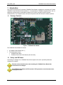
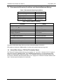
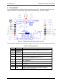
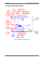
Simplifying System IntegrationTM
73S8009C
Demo Board User Manual
February 10, 2010
Rev. 1.3
UM_8009C_059
73S8009C Demo Board User Manual
UM_8009C_059
© 2010 Teridian Semiconductor Corporation. All rights reserved.
Teridian Semiconductor Corporation is a registered trademark of Teridian Semiconductor Corporation.
Simplifying System Integration is a trademark of Teridian Semiconductor Corporation.
All other trademarks are the property of their respective owners.
Teridian Semiconductor Corporation makes no warranty for the use of its products, other than expressly
contained in the Company’s warranty detailed in the Teridian Semiconductor Corporation standard Terms
and Conditions. The company assumes no responsibility for any errors which may appear in this
document, reserves the right to change devices or specifications detailed herein at any time without
notice and does not make any commitment to update the information contained herein. Accordingly, the
reader is cautioned to verify that this document is current by comparing it to the latest version on
http://www.teridian.com or by checking with your sales representative.
Teridian Semiconductor Corp., 6440 Oak Canyon, Suite 100, Irvine, CA 92618
TEL (714) 508-8800, FAX (714) 508-8877, http://www.teridian.com
2
Rev. 1.3
UM_8009C_059
73S8009C Demo Board User Manual
Table of Contents
1
Introduction ................................................................................................................................... 5
1.1 Package Contents.................................................................................................................... 5
1.2 Safety and ESD Notes ............................................................................................................. 5
1.3 Recommended Operating Conditions and Absolute Maximum Ratings ..................................... 6
1.4 Notes When Using a 73S12xxF Evaluation Board .................................................................... 6
2
Connections................................................................................................................................... 7
3
Jumpers, Switches and Test Points ............................................................................................. 9
4
Design Considerations ................................................................................................................ 12
4.1 General Layout Rules ............................................................................................................ 12
4.2 Optimization for Compliance with EMV................................................................................... 12
4.3 Power Supply Input Configurations ........................................................................................ 12
4.3.1 USB Power ................................................................................................................. 12
4.3.2 Single Supply Power ................................................................................................... 12
4.4 ON/OFF Switch Operation ..................................................................................................... 13
5
73S8009C Demo Board Schematics, PCB Layouts and Bill of Materials .................................. 14
5.1 Schematics ............................................................................................................................ 14
5.2 73S8009C PCB Layouts ........................................................................................................ 15
5.3 73S8009C Demo Board Bill of Materials................................................................................. 18
6
Errata............................................................................................................................................ 18
7
Ordering Information ................................................................................................................... 19
8
Related Documentation ............................................................................................................... 19
9
Contact Information..................................................................................................................... 19
Revision History .................................................................................................................................. 20
Rev. 1.3
3
73S8009C Demo Board User Manual
UM_8009C_059
Figures
Figure 1: 73S8009C Demo Board ............................................................................................................ 5
Figure 2: 73S8009C Demo Board External Connectors ............................................................................ 7
Figure 3: 73S8009C Demo Board Description.......................................................................................... 9
Figure 4: 73S8009C Electrical Schematic .............................................................................................. 14
Figure 5: 73S8009C Demo Board: Top View.......................................................................................... 15
Figure 6: 73S8009C Demo Board: Bottom View..................................................................................... 15
Figure 7: 73S8009C Demo Board: Top Signal Layer .............................................................................. 16
Figure 8: 73S8009C Demo Board: Middle Layer 1, Ground Plane .......................................................... 16
Figure 9: 73S8009C Demo Board: Middle Layer 2, Supply Plane ........................................................... 17
Figure 10: 73S8009C Demo Board: Bottom Signal Layer ....................................................................... 17
Tables
Table 1: Recommended Operating Conditions ......................................................................................... 6
Table 2: Absolute Maximum Ratings ........................................................................................................ 6
Table 3: J4 Pin Descriptions .................................................................................................................... 7
Table 4: J2 Pin Descriptions .................................................................................................................... 8
Table 5: 73S8009C Demo Board Description ......................................................................................... 10
Table 6: 73S8009C Demo Board Bill of Materials ................................................................................... 18
Table 7: 73S8009C Demo Board Order Number .................................................................................... 19
4
Rev. 1.3
UM_8009C_059
73S8009C Demo Board User Manual
1 Introduction
The Teridian Semiconductor Corporation 73S8009C Demo Board is a platform for evaluating the Teridian
73S8009C 32-pin QFN Smart Card Interface IC. It incorporates the 73S8009C integrated circuit, and it is
designed to operate either as a standalone platform (to be used in conjunction with an external
microcontroller) or as a daughter card to be used in conjunction with the 73S12xxF evaluation platform.
1.1
Package Contents
Figure 1: 73S8009C Demo Board
The 73S8009C Demo Board Kit includes:
•
•
1.2
A 73S8009C Demo Board (Rev. 1)
The following documents:
• 73S8009C Data Sheet
• 73S8009C Demo Board User Manual (this document)
Safety and ESD Notes
Connecting live voltages to the 73S8009C Demo Board system will result in potentially hazardous
voltages on the boards.
Extreme caution should be taken when handling the 73S8009C Demo Board after
connection to live voltages!
The 73S8009C Demo Board is ESD sensitive! ESD precautions should be taken when
handling this board!
Rev. 1.3
5
73S8009C Demo Board User Manual
1.3
UM_8009C_059
Recommended Operating Conditions and Absolute Maximum Ratings
Table 1: Recommended Operating Conditions
Parameter
Rating
Supply Voltage VPC
2.7 to 6.5 VDC
Supply Voltage VBUS
4.4 to 5.5 VDC
Supply Voltage VBAT
4.0 to 6.5 °C
Ambient Operating Temperature
-40 °C to +85 °C
Table 2: Absolute Maximum Ratings
Parameter
Rating
Supply Voltage VBUS
-0.5 to 6.6 VDC
Supply Voltage VBAT
-0.5 to 6.6 VDC
Supply Voltage VPC
-0.5 to 6.6 VDC
Input Voltage for Digital Inputs
-0.3 to (VDD+0.5) VDC
Storage Temperature
-60 to 150 °C
Pin Voltage (except card interface)
-0.3 to (VDD+0.5) VDC
Pin Voltage (card interface)
-0.3 to (VCC+0.3) VDC
Pin Voltage, LIN pin
0.3 to 6.5 VDC
ESD Tolerance – Card interface pins
± 6 kV
ESD Tolerance – Other pins
± 2 kV
Pin Current
± 200 mA
Operation outside these rating limits may cause permanent damage to the device.
ESD testing on Card pins is HBM condition, 3 pulses, each polarity referenced to ground.
1.4
Notes When Using a 73S12xxF Evaluation Board
The 73S12xxF Evaluation Board has two power supplies; 3.3 V and 5.0 V. Normally, the 5.0 V supply is
tied to VPC IN on the 73S8009C board. The 73S8009C can supply the 3.3 V to the remainder of the
system by configuring the jumpers accordingly. The 73S8009C VDD output can be disconnected from
the rest of the evaluation board if desired and the 3.3 V supply on the 73S12xxF Evaluation Board can be
used. See the jumper descriptions for more details.
6
Rev. 1.3
UM_8009C_059
73S8009C Demo Board User Manual
2 Connections
This section describes the 73S8009C Demo Board external connectors. All the digital signals and power
supply connections are made through 10-pin header connectors labeled J2 and J4 in Figure 2.
Figure 2: 73S8009C Demo Board External Connectors
Table 3 describes the pins for the J4 connector. There is one power pin (Pin 1) and one ground pin (Pin 9).
Table 3: J4 Pin Descriptions
Rev. 1.3
Pin
Pin Name
1
CMDVCC%
2
CMDVCC#
3
RSTIN
Controls the card reset signal.
4
RDY
Indicates when smart card power supply is stable and ready.
5
OFF_ACK
Setting OFF_ACK high powers “off” all analog functions and
disconnects the 73S8009C from VBAT or VPC.
6
OFF_REQ
Digital output. Request to the host system controller to turn
the 73S8009C off.
7
CS
Chip Select – active high.
8
N/C
No Connect.
9
GND
Ground.
10
VDD
System interface supply voltage and supply voltage for
companion controller circuitry.
Function
Controls the turn-on, output voltage value, and turn-off of VCC.
7
73S8009C Demo Board User Manual
UM_8009C_059
Table 4 describes the J2 connector pins.
Table 4: J2 Pin Descriptions
Pin
Pin Name
Function
1
SCLK
Clock source input.
2
I/OUC
System controller data I/O to/from the card.
3
SC4
System controller auxiliary data C4 to/from the card.
4
SC8
System controller auxiliary data C8 to/from the card.
5
OFF
Interrupt signal to the processor. Indicator of card presence
and any card fault conditions.
6
GND
Ground.
7
GND
Ground.
8
GND
Ground.
9
VPC IN
Must be between 2.7 V and 6.5 V.
10
VPC IN
Must be between 2.7 V and 6.5 V.
Connections should be made in this order:
• Power Supplies: Apply 3.3 V to pin 10 of J4 or 5 V to pins 9 and 10 of J2 depending on the setting of
JP2.
• Press the ON/OFF button.
• Control signals to the device can be connected through J2 and J4. See Figure 2 and Figure 4.
• Apply the clock signal.
8
Rev. 1.3
UM_8009C_059
73S8009C Demo Board User Manual
3 Jumpers, Switches and Test Points
The items marked in Figure 3 are described in Table 5.
Figure 3: 73S8009C Demo Board Description
Rev. 1.3
9
73S8009C Demo Board User Manual
UM_8009C_059
Table 5: 73S8009C Demo Board Description
Item #
(Figure 3)
10
Electrical
Schematic &
PCB Silkprint
Reference
Name
1
S1
ON/OFF switch
Push-button switch to turn on/off the 73S8009C.
Note: OFF_ACK must be set high to turn off.
2
JP3
ON_OFF Jumper
When set to 1-2, the ON_OFF input is set to ground
which turns on the 73S8009C when power is
applied. When set to 2-3, the push button switch is
connected to the ON_OFF pin.
When using VBUS as an always on configuration,
JP3 must be set to the 1-2 position and the
OFF_ACK input must be grounded.
3
JP2
VPC Select
The VPC input can select between the VPC_IN and
the 3.3 V inputs. When selecting the VPC_IN, the
VDD output can source the 3.3 V supply on the
evaluation board. See the description for JP4.
4
5
6
7
8
9
12
13
TP1
TP2
TP8
TP7
TP5
TP3
TP4
TP6
Test Points:
VBAT Test point
VBUS Test point
C4
CLK
RST
VCC
I/O
C8
10
J4
Board 3.3 V
supply and digital
control signals
Connector that either gathers or supplies the 3.3 V
supply. It includes the 73S8009C host control
signal pins RDY, CS, OFF_REQ, OFF_ACK,
CMDVCC%, CMDVCC#, and RSTIN.
11
J6
Smart Card
Connector
SIM/SAM smart card format connector.
Note that J6 is wired in parallel to the smart card
connector J5 (underneath the PCB). J5 and J6 are
never to be used at the same time.
14
JP4
VDD Select
When the jumper is inserted, the 73S8009C VDD
output is connected to the 3.3 V power plane.
When using in conjunction with a 73S12xxF
Evaluation Board or other host, it supplies the 3.3 V
source on the on that platform if it is so configured.
Caution must be taken as damage could occur if the
73S12xxF Evaluation Board or host is sourcing
3.3 V with this jumper inserted. Removal of the
jumper provides proper isolation with any host
platform.
Use
VBAT Input
VBUS Input
Two-pin test points for each respective smart card
signal. The pin label name is the respective signal
(i.e. VCC, CLK) and the other pin is GND.
Rev. 1.3
UM_8009C_059
Item #
(Figure 3)
73S8009C Demo Board User Manual
Electrical
Schematic &
PCB Silkprint
Reference
Name
15
18
JP6
JP5
Card Polarity
detect select
The setting of these two jumpers depends on the
type of smart card connector used (whether switch
is nominally open or closed), and which of the card
presence switch input of the 73S8009C is used. In
this demo board, the switch is nominally open. The
jumpers can be set in one of two ways:
1. Default setting: Use of PRES: JP5 must be
set to PRES, and JP6 set to VDD
2. Alternative use: Use of PRES: JP5 must be
set to PREB, and JP6 set to GND
Note: see board errata in the appendix for JP6
16
J5
Smart Card
Connector
Smart card connector.
When inserting a card (credit card size format),
contacts must face up.
17
JP7
CS Disable
CS Disable Jumper. Insertion of jumper disables
the 73S8009CN. The state of the CMDVCC#,
CMDVCC% and RSTIN inputs will be latched and
the I/OUC, AUX1UC and AUX2UC are tri-stated.
The OFF and RDY outputs are also tri-stated.
19
TP9
Vp Test Point
Test point to monitor the internal intermediate
voltage regulator. This regulator output takes the
VPC voltage and step it up to more than 5 V (if
necessary) as the input source for the VCC and
VDD output regulators.
20
J3
Board VPC_IN
supply, smart
card data signals
and OFF
Connector that supplies the VPC input supply
voltage, the smart card data interface signals and
the OFF interrupt output.
Rev. 1.3
Use
11
73S8009C Demo Board User Manual
UM_8009C_059
4 Design Considerations
4.1
General Layout Rules
Follow these layout rules:
•
•
•
Route I/O and auxiliary signals away from card interface signals.
Keep CLK trace as short as possible and with minimal bends in the trace. If possible, keep routing of
the CLK trace to one layer (avoid vias to other layers). Keep CLK trace away from other traces
especially RST, I/O and VCC. Filtering of the CLK trace is allowed for noise purposes. Up to 30 pF
to ground is allowed at the CLK pin of the smart card connector. Also, the zero Ω series resistor (R7)
can be replaced with a small resistor for additional filtering (no more than 100 Ω).
Keep VCC trace as short as possible. Make trace a minimum of 0.5 mm thick. Also, keep VCC away
from other traces especially RST and CLK.
•
•
•
Keep RST trace away from VCC and CLK traces. Up to 30 pF to ground is allowed for filtering.
Keep 0.1 µF close to VDD pin of the device and directly take other end to ground.
Keep 0.1 µF and 10 µF close to VPC pin of the device and directly take other end to ground.
•
Keep 4.7 µF close to VP pin of the device and directly take other end to ground.
•
Keep 0.47 µF close to VCC pin of the smart card connector and directly take other end to ground.
4.2
Optimization for Compliance with EMV
Default configuration of the Demo board contains a 27 pF capacitor (C12) from the CLK pin of the smart
connector to ground and a 27 pF capacitor (C13) from the RST pin of the smart connector to ground.
These capacitors serve as filters for CLK and RST signals in the case of long traces or test equipment
perturbations. The capacitor on CLK reduces ringing on the trace, reduces coupling to other traces and
slows down the edge of the CLK signal. The capacitor on RST helps the perturbation specification in a
noisy environment. The filter capacitors can be useful in the EMV test environment and have no effect on
NDS testing
C12 and C13 are represented on both schematic and BOM. These capacitors are optional filter
capacitors on the smart card lines CLK and RST, respectively for each card interface. These capacitors
may be adjusted (value, not to exceed 30 pF) or removed to optimize performance in each specific
application (PCB, card clock frequency, compliance with applicable standards etc).
4.3
Power Supply Input Configurations
4.3.1 USB Power
The USB configuration uses the power supplied by the VBUS (4.4 to 5.5 V) and an optional VBAT input
that automatically switches from the VBUS to VBAT when the VBUS power is removed. This switch over
is done smoothly and does not cause any disruption of the operation of the 73S8009C and the VDD
output supply. The operation of the ON/OFF switch is overridden when VBUS is applied. The 73S8009C
and VDD output will always be active while the VBUS voltage is applied. The ON/OFF switch is enabled
when running off VBAT. When using this configuration, the VPC input should not be connected to any
other power source.
4.3.2 Single Supply Power
The single supply configuration should leave the VBUS and VBAT pins unconnected and only connect
the power supply to VPC (2.7 to 6.0 V).
12
Rev. 1.3
UM_8009C_059
4.4
73S8009C Demo Board User Manual
ON/OFF Switch Operation
The ON/OFF switch uses a pushbutton to toggle between turning the 73S8009C on and off. The switch
input contains a debounce circuit for protection. The 73S8009C defaults to the OFF state when the
power source is applied. When the 8009C is in the OFF state, a switch closure turns on the 73S8009C.
When the 73S8009C is ON, a switch closure does not turn off the 73S8009C by itself, but it activates the
OFF_REQ signal by setting it high. The 73S8009C does not shut off until the OFF_ACK is set high. The
purpose of this sequence is to allow the host processor to perform any necessary shut down tasks before
losing power. When the host is finished, it can set the OFF_ACK signal high to shut off the 73S8009C. If
there is no need for the host to perform any shutdown tasks, the OFF_ACK pin can be left open and it
follows the state of the OFF_REQ output by means of an internal resistor connection between the
OFF_REQ and OFF_ACK pins.
When power is applied to VBUS, the 73S8009C automatically turns on and the ON/OFF switch is
overidden. However, care must be taken as the ON_OFF input is internally latched while the VBUS
is applied. When VBUS is removed, the latched state of the ON/OFF switch input dictates the state
of the 73S8009C. If the switch input was not closed, the state of this latch will not change. It will be
in the same state before the VBUS power was applied. If it has changed it holds the last toggled
state. The OFF_REQ output follows this toggling. If the OFF_REQ output is high when VBUS
power is removed and the OFF_ACK is high, the 73S8009C shuts off.
Rev. 1.3
13
73S8009C Demo Board User Manual
UM_8009C_059
5 73S8009C Demo Board Schematics, PCB Layouts and Bill of Materials
Schematics
L1
1
1
2
3
4
5
6
7
8
IOUC
AUX1UC
AUX2UC
CMDVCC5
CMDVCC3
RSTIN
CLKIN
RDY
73S8009C
TP1
1
ON/OFF
VBUS
IO
AUX1
AUX2
VCC
RST
GND
TP2
1
2
3
JP3
OFF
GND
TEST2
VDD
GND
LIN
VPC
VBAT
33
U1
OFF_ACK
TEST1
OFF_REQ
CS
PRES
PRES
VP
CLK
1
2
3
4
5
6
7
8
9
10
C1, C2, C3 and L1 must be placed
within 5mm of the U1 pins and
connected by thick track (wider
than 0.5mm)
OFF
C3
0.1uF
SLUG
J3
0.1uF
VDD
1
2
VPCIN
IOUC
AUX1UC
AUX2UC
CMDVCC%
CMDVCC#
RSTIN
CLKIN
RDY
10uF
C2
32
31
30
29
28
27
26
25
Note: JP4 pins 1
and 2 should only
be connected when
3.3V is not sourced
from the mating
board (if
applicable)
C1
3.3V
JP4
S1
SW
1
24
23
22
21
20
19
18
17
2
IO
AUX1
AUX2
VCC
RST
R8
Ru
DNI
R9
Ru
DNI
9
10
11
12
13
14
15
16
Note: JP4 pins 1
and 2 must not be
connected with JP2
pins 1 and 2 at the
same time.
TSM_110_01_L_SV
CMDVCC5
CMDVCC3
RSTIN
RDY
OFF_ACK
OFF_REQ
CS
USR7
GND
+3.3V
VPC
SELECT
3.3V
J2
1
2
3
4
5
6
7
8
9
10
VPCIN
1
2
3
1
2
3
4
5
6
7
8
9
10
SSM_110_L_SV
Note: VPCIN
must be
between 2.7
and 6.5V
JP2
3.3V
J1
SCLK
SIO
SC4
SC8
OFF
GND
GND
GND
VPCIN
VPCIN
+
5.1
SSM_110_L_SV
R7 0
R8 to R13 and C36 to be
placed within 1cm of
J7.
CLK
J4
TP9
1
C4
OFF_ACK
OFF_REQ
CS
R12
Rd
DNI
JP7
3.3V
CS
Disable
TSM_110_01_L_SV
1
2
R10
Ru
DNI
TP3
1
2
J2 and J4
TP4
R13
Rd
DNI
J1 and J3 must be aligned with J8 and J9 on the
1121 evaluation board (E1121T8) respectivly in
order for this board to be stacked on it.
I/O
1
2
TP6
C8
J1 must be aligned with J2 and J3 must be
aligned with J4 in order for this daughter
board to be stacked on another.
PRES
JP5
CARD DETECT
POLARITY
SELECT
RST
TP7
1
2
1
2
PRES
PRES
1
2
3
VCC
TP5
1
2
CLK
TP8
1
2
C4
TP3 to TP8, C9, C11 and
C12 are to be placed
very close to the pads
of J5
PRES
JP6
VDD
VDD
1
2
3
C9
C11
30pF
30pF
0.47uF
J5
Smart Card Connector
SW2
SW1
C7
C6
C5
C3
C2
C1
C8
I/O
VPP
GND
C4
CLK
RST
VCC
SW-2
SW-1
8
7
6
5
4
3
2
1
GND
C12
8
7
6
5
4
3
2
1
J1 and J3 are placed on the bottom.
are placed on the top side.
R11
Rd
DNI
4.7uF
10
9
1
2
3
4
5
6
7
8
9
10
J6
SIM/SAM Connector
Figure 4: 73S8009C Electrical Schematic
14
Rev. 1.3
UM_8009C_059
5.2
73S8009C Demo Board User Manual
73S8009C PCB Layouts
Figure 5: 73S8009C Demo Board: Top View
Figure 6: 73S8009C Demo Board: Bottom View
Rev. 1.3
15
73S8009C Demo Board User Manual
UM_8009C_059
Figure 7: 73S8009C Demo Board: Top Signal Layer
Figure 8: 73S8009C Demo Board: Middle Layer 1, Ground Plane
16
Rev. 1.3
UM_8009C_059
73S8009C Demo Board User Manual
Figure 9: 73S8009C Demo Board: Middle Layer 2, Supply Plane
Figure 10: 73S8009C Demo Board: Bottom Signal Layer
Rev. 1.3
17
73S8009C Demo Board User Manual
5.3
UM_8009C_059
73S8009C Demo Board Bill of Materials
Table 6: 73S8009C Demo Board Bill of Materials
Qnt Reference
Part
PCB Footprint
Digikey Part
Number
Part Number
Manufacturer
1
C1
10 µF
805
PCC2225CT-ND
ECJ-2FB0J106M
Panasonic
2
C2, C3
0.1 µF
603
PCC1762CT-ND
ECJ-1VB1C104K
Panasonic
1
C4
4.7 µF
603
PCC2396CT-ND
ECJ-1VB0J475K
Panasonic
2
C9, C12
27 pF
603
PCC270ACVCTND
ECJ-1VC1H270J
Panasonic
1
C11
0.47 µF
603
PCC2275CT-ND
ECJ-1VB0J475K
Panasonic
4
JP2, JP3,
JP5, JP6
Header 3
3pins, 2.54mm pitch S1011E-36-ND
PBC36SAAN
Sullins
2
JP4, JP7
Header 2
2pins, 2.54mm pitch S1011E-36-ND
PBC36SAAN
Sullins
2
J1, J3
SSM_110_L_SV
SSM_110_L_SV
X
SSM_110_L_SV
Samtec
2
J2, J4
TSM_110_01_L_SV
TSM_110_01_L_SV
X
TSM_110_01_L_SV
Samtec
1
J5
Smart Card Connector
ITT_CCM02-2504
401-1715-ND
CCM02-2504LFT
ITTCannon
1
J6
SIM/SAM Connector
CCM03-3754
ITTCannon
1
L1
Inductor
445-1998-1-ND
SLF7032T100M1R4-2-PF
TDK
2
R7
0
603
P0.0GCT-ND
ERJ-3GEY0R00V
Panasonic
1
S1
Switch
Panasonic EVQ
P8051SCT
EVQ-PJX05M
Panasonic
8
TP1, TP2,
TP3, TP4,
TP5, TP6,
TP7, TP8
TP
2X1_Header
S1011E-36-ND
PBC36SAAN
Sullins
1
U1
73S8009C
32QFN
X
73S8009C
Teridian
ITT_CCM03-3754 CCM03-3754CTND
Note: The resistors noted Ru and Rd in the schematic are not populated on the board. They can be
implemented to adjust the features of the smart card reader.
6 Errata
The 73S8009C Demo Board contains a silk screen error on JP6. The VDD and GND are reversed and
have corrective decals attached to show the proper labeling.
18
Rev. 1.3
UM_8009C_059
73S8009C Demo Board User Manual
7 Ordering Information
Table 7 lists the order number used to identify the 73S8009C Demo Board.
Table 7: 73S8009C Demo Board Order Number
Part Description
Order Number
73S8009C 32-Pin QFN Demo Board
73S8009C-DB
8 Related Documentation
The following 73S8009C documents are available from Teridian Semiconductor Corporation:
73S8009C Data Sheet
73S8009C Demo Board User Manual
9 Contact Information
For more information about Teridian Semiconductor products or to check the availability of the
73S8009C, contact us at:
6440 Oak Canyon Road
Suite 100
Irvine, CA 92618-5201
Telephone: (714) 508-8800
FAX: (714) 508-8878
Email: [email protected]
For a complete list of worldwide sales offices, go to http://www.teridian.com.
Rev. 1.3
19
73S8009C Demo Board User Manual
UM_8009C_059
Revision History
Revision
Date
Description
1.0
5/22/2007
First publication.
1.1
8/9/2007
Corrected schematic error.
1.2
9/6/2007
Corrected pin number for OFF_ACK in pin description.
1.3
2/10/2010
Formatted in the new Teridian style.
Added Section 1.1, Package Contents.
Added Section 1.2, Safety and ESD Notes.
Added Table 3: J4 Pin Descriptions.
Added Table 4: J2 Pin Descriptions.
Added Section 7, Ordering Information.
Added Section 8, Related Documentation.
Added Section 9, Contact Information.
Miscellaneous editorial corrections.
20
Rev. 1.3