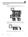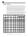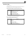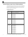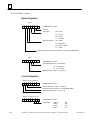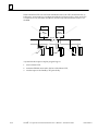
1
ÎÎ
GE Fanuc Automation
Programmable Control Products
t
Genius I/O
System and Communications
User’s Manual
GEK-90486F -1
November 1994
GFL–002
Warnings, Cautions, and Notes
as Used in this Publication
Warning
Warning notices are used in this publication to emphasize that hazardous voltages, currents, temperatures, or other conditions that could cause personal injury exist in this
equipment or may be associated with its use.
In situations where inattention could cause either personal injury or damage to equipment, a Warning notice is used.
Caution
Caution notices are used where equipment might be damaged if care is not taken.
Note
Notes merely call attention to information that is especially significant to understanding
and operating the equipment.
This document is based on information available at the time of its publication. While efforts have been made to be accurate, the information contained herein does not purport
to cover all details or variations in hardware or software, nor to provide for every possible contingency in connection with installation, operation, or maintenance. Features
may be described herein which are not present in all hardware and software systems.
GE Fanuc Automation assumes no obligation of notice to holders of this document with
respect to changes subsequently made.
GE Fanuc Automation makes no representation or warranty, expressed, implied, or statutory with respect to, and assumes no responsibility for the accuracy, completeness, sufficiency, or usefulness of the information contained herein. No warranties of merchantability or fitness for purpose shall apply.
The following are trademarks of GE Fanuc Automation North America, Inc.
Alarm Master
CIMSTAR
Helpmate
PROMACRO
Series Six
CIMPLICITY
Field Control
GEnet
Logicmaster
Series One
Series 90
CIMPLICITY
90–ADS
Genius
Modelmaster
Series Three
VuMaster
CIMPLICITY PowerTRAC
Copyright 1986 – 1994 GE Fanuc Automation North America, Inc.
All Rights Reserved
Genius PowerTRAC
ProLoop
Series Five
Workmaster
Preface
The Genius I/O System User’s Manual is Volume 1 of a two–book set. It is a reference to
the features, installation, communications capabilities, and operation of systems using
Genius products.
Volume 2 of the set, the Genius Discrete and Analog Blocks User’s Manual describes the
features, installation, configuration, and operation of discrete and analog blocks.
Content of this Volume
This Volume covers the following topics:
Chapter 1. Introduction: provides basic information about the elements of a Genius
system.
Chapter 2. The Communications Bus: describes the selection and installation of the bus
cable that links Genius devices. It also explains how fiber optics cable and modems can
be utilized in certain applications.
Chapter 3. Datagrams: describes datagram messages that may be sent or received by a
bus controller.
Chapter 4. Configuration Data Formats: shows the formats of configuration data for all
Genius blocks, and for Series Six bus controllers.
Chapter 5. Diagnostics Data Formats: shows the formats of diagnostics data for all
Genius blocks, for Series Six bus controllers, and for Series 90 bus controllers.
Chapter 6. Read Block I/O Reply Data Formats: shows the formats of data returned by
some Genius blocks in response to a Read Block I/O datagram.
Chapter 7. Global Data: describes how Global Data works, and explains basic
differences between Global Data and datagrams.
Chapter 8. Data Monitoring, Redundant Control, and Distributed Control: describes
advanced systems that can be set up.
Chapter 9. Timing Considerations: explains how to determine bus scan time and how
to calculate I/O response time, and describes the relationship between bus scan time and
CPU sweep time.
Chapter 10. Troubleshooting: contains basic fault–isolation and correction procedures.
Appendix A. Product Compatibility, Catalog Numbers, and Publication Numbers: is a
reference to currently–available Genius products, previously–available products, and
device compatibilities.
GEK-90486F-1
iii
Preface
Related Publications
Series 90–70 Bus Controller User’s Manual (GFK–0398)
Series 90–30 Bus Controller User’s Manual (GFK–1034)
Series 90–30 Enhanced Genius Communications Module User’s Manual (GFK–0695)
Series 90–30 Genius Communications Module User’s Manual (GFK–0412)
Series Six Bus Controller User’s Manual (GFK–0171)
Series Five Bus Controller User’s Manual (GFK–0248)
PCIM User’s Manual (GFK–0074)
Genius PowerTRAC Block User’s Manual (GFK–0450)
Genius High–speed Counter Block User’s Manual (GFK–0415)
Logicmaster 90–70 User’s Manual (GFK–0263)
Series 90–70 Remote I/O Scanner User’s Manual (GFK–0579)
Refer to appendix A for a complete listing of Genius product manuals and data sheets.
We Welcome Your Comments and Suggestions
At GE Fanuc automation, we strive to produce quality technical documentation. After
you have used this manual, please take a few moments to complete and return the
Reader ’s Comment Card located on the next page.
Jeanne L. Grimsby
Senior Technical Writer
iv
t I/O System and Communications User’s Manual
Genius
GEK-90486F-1
Contents
Chapter 1
Chapter 2
GEK-90486F-1
Introduction . . . . . . . . . . . . . . . . . . . . . . . . . . . . . . . . . . . . . . . . . . . . . . .
1-1
CPUs and Bus Controllers . . . . . . . . . . . . . . . . . . . . . . . . . . . . . . . . . . . . . . . . . .
1-2
The Hand-held Monitor . . . . . . . . . . . . . . . . . . . . . . . . . . . . . . . . . . . . . . . . . . .
1-4
Genius Blocks . . . . . . . . . . . . . . . . . . . . . . . . . . . . . . . . . . . . . . . . . . . . . . . . . . . .
1-6
Bus and Communications Overview . . . . . . . . . . . . . . . . . . . . . . . . . . . . . . . .
1-13
System Operation . . . . . . . . . . . . . . . . . . . . . . . . . . . . . . . . . . . . . . . . . . . . . . . .
1-15
I/OService and Diagnostics . . . . . . . . . . . . . . . . . . . . . . . . . . . . . . . . . . . . . . . .
1-16
Datagrams and Global Data . . . . . . . . . . . . . . . . . . . . . . . . . . . . . . . . . . . . . . . .
1-18
Features and Benefits . . . . . . . . . . . . . . . . . . . . . . . . . . . . . . . . . . . . . . . . . . . . .
1-19
Planning Guidelines . . . . . . . . . . . . . . . . . . . . . . . . . . . . . . . . . . . . . . . . . . . . . .
1-20
The Communications Bus . . . . . . . . . . . . . . . . . . . . . . . . . . . . . . . . . . .
2-1
Wiring Guidelines . . . . . . . . . . . . . . . . . . . . . . . . . . . . . . . . . . . . . . . . . . . . . . . .
2-1
Selecting a Cable Type . . . . . . . . . . . . . . . . . . . . . . . . . . . . . . . . . . . . . . . . . . . . .
2-2
Bus Length . . . . . . . . . . . . . . . . . . . . . . . . . . . . . . . . . . . . . . . . . . . . . . . . . . . . . .
2-4
Baud Rate Selection . . . . . . . . . . . . . . . . . . . . . . . . . . . . . . . . . . . . . . . . . . . . . . .
2-4
Connecting Devices to the Bus . . . . . . . . . . . . . . . . . . . . . . . . . . . . . . . . . . . . . .
2-5
Bus Ambient Electrical Information . . . . . . . . . . . . . . . . . . . . . . . . . . . . . . . . .
2-9
Using a Dual Bus . . . . . . . . . . . . . . . . . . . . . . . . . . . . . . . . . . . . . . . . . . . . . . . . .
2-9
Using Fiber Optics . . . . . . . . . . . . . . . . . . . . . . . . . . . . . . . . . . . . . . . . . . . . . . . .
2-10
Genius I/O System and Communications User’s Manual – November 1994
v
Contents
Chapter 3
GEK-90486F-1
Datagrams . . . . . . . . . . . . . . . . . . . . . . . . . . . . . . . . . . . . . . . . . . . . . . . .
3-1
Types of Datagrams . . . . . . . . . . . . . . . . . . . . . . . . . . . . . . . . . . . . . . . . . . . . . . .
3-2
Datagram Operation . . . . . . . . . . . . . . . . . . . . . . . . . . . . . . . . . . . . . . . . . . . . . .
3-3
Application Programming for Datagrams . . . . . . . . . . . . . . . . . . . . . . . . . . . .
3-6
Read Identification . . . . . . . . . . . . . . . . . . . . . . . . . . . . . . . . . . . . . . . . . . . . . . . .
3-8
Read Identification Reply . . . . . . . . . . . . . . . . . . . . . . . . . . . . . . . . . . . . . . . . . .
3-8
Read Configuration . . . . . . . . . . . . . . . . . . . . . . . . . . . . . . . . . . . . . . . . . . . . . . .
3-11
Read Configuration Reply . . . . . . . . . . . . . . . . . . . . . . . . . . . . . . . . . . . . . . . . .
3-11
Write Configuration . . . . . . . . . . . . . . . . . . . . . . . . . . . . . . . . . . . . . . . . . . . . . . .
3-11
Assign Monitor . . . . . . . . . . . . . . . . . . . . . . . . . . . . . . . . . . . . . . . . . . . . . . . . . . .
3-12
Begin Packet Sequence . . . . . . . . . . . . . . . . . . . . . . . . . . . . . . . . . . . . . . . . . . . .
3-13
End Packet Sequence . . . . . . . . . . . . . . . . . . . . . . . . . . . . . . . . . . . . . . . . . . . . . .
3-13
Read Diagnostics . . . . . . . . . . . . . . . . . . . . . . . . . . . . . . . . . . . . . . . . . . . . . . . . .
3-14
Read Diagnostics Reply . . . . . . . . . . . . . . . . . . . . . . . . . . . . . . . . . . . . . . . . . . . .
3-14
Write Point . . . . . . . . . . . . . . . . . . . . . . . . . . . . . . . . . . . . . . . . . . . . . . . . . . . . . . .
3-15
Read Block I/O . . . . . . . . . . . . . . . . . . . . . . . . . . . . . . . . . . . . . . . . . . . . . . . . . . .
3-16
Read Block I/O Reply . . . . . . . . . . . . . . . . . . . . . . . . . . . . . . . . . . . . . . . . . . . . .
3-16
Report Fault . . . . . . . . . . . . . . . . . . . . . . . . . . . . . . . . . . . . . . . . . . . . . . . . . . . . .
3-17
Pulse Test . . . . . . . . . . . . . . . . . . . . . . . . . . . . . . . . . . . . . . . . . . . . . . . . . . . . . . . .
3-27
Pulse Test Complete . . . . . . . . . . . . . . . . . . . . . . . . . . . . . . . . . . . . . . . . . . . . . . .
3-27
Clear Circuit Fault . . . . . . . . . . . . . . . . . . . . . . . . . . . . . . . . . . . . . . . . . . . . . . . .
3-28
Clear All Circuit Faults . . . . . . . . . . . . . . . . . . . . . . . . . . . . . . . . . . . . . . . . . . . . .
3-28
Switch BSM . . . . . . . . . . . . . . . . . . . . . . . . . . . . . . . . . . . . . . . . . . . . . . . . . . . . . .
3-29
Read Device . . . . . . . . . . . . . . . . . . . . . . . . . . . . . . . . . . . . . . . . . . . . . . . . . . . . .
3-30
Read Device Reply . . . . . . . . . . . . . . . . . . . . . . . . . . . . . . . . . . . . . . . . . . . . . . . .
3-39
Write Device . . . . . . . . . . . . . . . . . . . . . . . . . . . . . . . . . . . . . . . . . . . . . . . . . . . . .
3-40
Configuration Change . . . . . . . . . . . . . . . . . . . . . . . . . . . . . . . . . . . . . . . . . . . . .
3-42
Read Data . . . . . . . . . . . . . . . . . . . . . . . . . . . . . . . . . . . . . . . . . . . . . . . . . . . . . . .
3-43
Read Data Reply . . . . . . . . . . . . . . . . . . . . . . . . . . . . . . . . . . . . . . . . . . . . . . . . .
3-43
Write Data . . . . . . . . . . . . . . . . . . . . . . . . . . . . . . . . . . . . . . . . . . . . . . . . . . . . . . .
3-44
Read Map . . . . . . . . . . . . . . . . . . . . . . . . . . . . . . . . . . . . . . . . . . . . . . . . . . . . . . .
3-45
Read Map Reply . . . . . . . . . . . . . . . . . . . . . . . . . . . . . . . . . . . . . . . . . . . . . . . . . .
3-45
Write Map . . . . . . . . . . . . . . . . . . . . . . . . . . . . . . . . . . . . . . . . . . . . . . . . . . . . . . .
3-45
Assign SBA #29 to Hot Standby Operation . . . . . . . . . . . . . . . . . . . . . . . . . . .
3-46
Genius I/O System and Communications User’s Manual – November 1994
vi
Contents
Chapter 4
Chapter 5
Chapter 6
Chapter 7
GEK-90486F-1
Configuration Data Formats . . . . . . . . . . . . . . . . . . . . . . . . . . . . . . . . .
4-1
Discrete I/O Blocks (except 16-Circuit 115VAC Input Blocks) . . . . . . . . . . . .
4-2
16 Circuit 115VAC Input Block . . . . . . . . . . . . . . . . . . . . . . . . . . . . . . . . . . . . . .
Voltage/Current 4 Input/2 Output Analog Blocks . . . . . . . . . . . . . . . . . . . . . .
Current-source Analog 4 Input/2 Output Blocks . . . . . . . . . . . . . . . . . . . . . . .
4-5
4-7
4-10
Current-source Analog 6-Output Blocks . . . . . . . . . . . . . . . . . . . . . . . . . . . . .
Current-source Analog 6-Input Blocks . . . . . . . . . . . . . . . . . . . . . . . . . . . . . . .
Thermocouple 6-Input Blocks . . . . . . . . . . . . . . . . . . . . . . . . . . . . . . . . . . . . . .
RTD 6-Input Blocks . . . . . . . . . . . . . . . . . . . . . . . . . . . . . . . . . . . . . . . . . . . . . . .
4-13
4-15
4-17
4-19
High-speed Counter Block, Configured as Type A . . . . . . . . . . . . . . . . . . . . .
High-speed Counter Block, Configured as Type B . . . . . . . . . . . . . . . . . . . . .
High-speed Counter Block, Configured as Type C . . . . . . . . . . . . . . . . . . . . .
PowerTRAC Block . . . . . . . . . . . . . . . . . . . . . . . . . . . . . . . . . . . . . . . . . . . . . . . .
4-21
4-24
4-27
4-30
Series Six Bus Controller . . . . . . . . . . . . . . . . . . . . . . . . . . . . . . . . . . . . . . . . . . .
4-32
Diagnostics Data Formats . . . . . . . . . . . . . . . . . . . . . . . . . . . . . . . . . . .
5-1
Differences Between Report Fault and Read Diagnostics Reply Datagrams
5-1
Discrete Blocks . . . . . . . . . . . . . . . . . . . . . . . . . . . . . . . . . . . . . . . . . . . . . . . . . . .
Analog, RTD, and Thermocouple Blocks . . . . . . . . . . . . . . . . . . . . . . . . . . . . .
High-speed Counter Block . . . . . . . . . . . . . . . . . . . . . . . . . . . . . . . . . . . . . . . . .
5-2
5-4
5-6
Series Six Bus Controller . . . . . . . . . . . . . . . . . . . . . . . . . . . . . . . . . . . . . . . . . . .
Series 90 Bus Controller . . . . . . . . . . . . . . . . . . . . . . . . . . . . . . . . . . . . . . . . . . .
5-7
5-9
Read Block I/O Reply Data Formats . . . . . . . . . . . . . . . . . . . . . . . . . .
6-1
Reading Block I/O Data . . . . . . . . . . . . . . . . . . . . . . . . . . . . . . . . . . . . . . . . . . . .
Voltage/Current 4 Input/2 Output Analog Blocks . . . . . . . . . . . . . . . . . . . . . .
Current-source Analog 4 Input/2 Output Blocks . . . . . . . . . . . . . . . . . . . . . . .
Current-source Analog 6-Output Blocks . . . . . . . . . . . . . . . . . . . . . . . . . . . . .
6-1
6-2
6-3
6-4
Current-source Analog 6-Input Blocks . . . . . . . . . . . . . . . . . . . . . . . . . . . . . . .
Thermocouple 6-Input Blocks . . . . . . . . . . . . . . . . . . . . . . . . . . . . . . . . . . . . . .
PowerTRAC Block . . . . . . . . . . . . . . . . . . . . . . . . . . . . . . . . . . . . . . . . . . . . . . . .
6-4
6-5
6-6
Global Data . . . . . . . . . . . . . . . . . . . . . . . . . . . . . . . . . . . . . . . . . . . . . . .
7-1
Global Data Devices . . . . . . . . . . . . . . . . . . . . . . . . . . . . . . . . . . . . . . . . . . . . . . .
Global Data Setup and Operation . . . . . . . . . . . . . . . . . . . . . . . . . . . . . . . . . . .
Global Data for the Series 90-70 PLC . . . . . . . . . . . . . . . . . . . . . . . . . . . . . . . . .
7-1
7-2
7-3
Global Data for the Series 90-30 PLC . . . . . . . . . . . . . . . . . . . . . . . . . . . . . . . . .
Global Data for the Series Six PLC . . . . . . . . . . . . . . . . . . . . . . . . . . . . . . . . . . .
Global Data for the Series Five PLC . . . . . . . . . . . . . . . . . . . . . . . . . . . . . . . . . .
7-5
7-9
7-11
Global Data for a Computer . . . . . . . . . . . . . . . . . . . . . . . . . . . . . . . . . . . . . . . .
Using Datagrams or Global Data . . . . . . . . . . . . . . . . . . . . . . . . . . . . . . . . . . . .
Timing Considerations . . . . . . . . . . . . . . . . . . . . . . . . . . . . . . . . . . . . . . . . . . . .
7-12
7-14
7-15
Genius I/O System and Communications User’s Manual – November 1994
vii
Contents
Chapter 8
Chapter 9
Chapter 10
Appendix A
GEK-90486F-1
Data Monitoring, Redundant Control, and Distributed Control . .
8-1
Data Monitoring . . . . . . . . . . . . . . . . . . . . . . . . . . . . . . . . . . . . . . . . . . . . . . . . . .
8-2
Bus and Bus Controller Redundancy . . . . . . . . . . . . . . . . . . . . . . . . . . . . . . . .
8-3
CPU Redundancy . . . . . . . . . . . . . . . . . . . . . . . . . . . . . . . . . . . . . . . . . . . . . . . .
8-9
Combining CPU Redundancy and Bus Cable Redundancy . . . . . . . . . . . . .
8-13
Shared Standby CPU . . . . . . . . . . . . . . . . . . . . . . . . . . . . . . . . . . . . . . . . . . . . . .
8-15
Distributed Control . . . . . . . . . . . . . . . . . . . . . . . . . . . . . . . . . . . . . . . . . . . . . . .
8-17
Timing Considerations . . . . . . . . . . . . . . . . . . . . . . . . . . . . . . . . . . . . .
9-1
Bus Scan Time . . . . . . . . . . . . . . . . . . . . . . . . . . . . . . . . . . . . . . . . . . . . . . . . . . . .
9-1
Displaying Bus Scan Time with a Hand-held Monitor . . . . . . . . . . . . . . . . . .
9-2
Estimating Bus Scan Time . . . . . . . . . . . . . . . . . . . . . . . . . . . . . . . . . . . . . . . . . .
9-3
Bus Scan Time for a Remote I/O Drop . . . . . . . . . . . . . . . . . . . . . . . . . . . . . . .
9-12
Estimating I/O Response Time for Blocks . . . . . . . . . . . . . . . . . . . . . . . . . . . . .
9-13
Relationship Between Bus Scan Time and Program Execution Time . . . . . .
9-16
Troubleshooting . . . . . . . . . . . . . . . . . . . . . . . . . . . . . . . . . . . . . . . . . . .
10-1
Replacement Modules . . . . . . . . . . . . . . . . . . . . . . . . . . . . . . . . . . . . . . . . . . . . .
10-1
To Begin: . . . . . . . . . . . . . . . . . . . . . . . . . . . . . . . . . . . . . . . . . . . . . . . . . . . . . . . .
10-1
Checking Cabling . . . . . . . . . . . . . . . . . . . . . . . . . . . . . . . . . . . . . . . . . . . . . . . . .
10-2
Bus and Bus Controller Troubleshooting . . . . . . . . . . . . . . . . . . . . . . . . . . . . .
10-2
I/O Block Troubleshooting . . . . . . . . . . . . . . . . . . . . . . . . . . . . . . . . . . . . . . . . .
10-4
Redundancy, Datagram, and Global Data Troubleshooting . . . . . . . . . . . . .
10-5
Hand-held Monitor Troubleshooting . . . . . . . . . . . . . . . . . . . . . . . . . . . . . . . .
10-6
Product Compatibility, Catalog Numbers, and Publications . . . . .
A-1
Phase A and Phase B Genius I/O Products . . . . . . . . . . . . . . . . . . . . . . . . . . . .
A-1
Catalog Numbers and Publication Numbers for Phase A Products . . . . . . .
A-2
Catalog Numbers and Publication Numbers for Phase B Products . . . . . . .
A-3
Catalog Numbers of Miscellaneous Accessories . . . . . . . . . . . . . . . . . . . . . . .
A-6
Product Compatibility . . . . . . . . . . . . . . . . . . . . . . . . . . . . . . . . . . . . . . . . . . . . .
A-8
Genius I/O System and Communications User’s Manual – November 1994
viii
Restarts for autonumbers that do not restart in each
chapter.
figure bi level 1, reset
table_big level 1, reset
chap_big level 1, reset1
app_big level 1, resetA
figure_ap level 1, reset
table_ap level 1, reset
figure level 1, reset
table level 1, reset
Chapter
these restarts must be in the header frame of chapter 1.
a:ebx, l 1 resetA
a:obx:l 1, resetA
a:bigbx level 1 resetA
a:ftr level 1 resetA
c:ebx, l 1 reset1
c:obx:l 1, reset1
c:bigbx level 1 reset1
c:ftr level 1 reset1
Reminders for autonumbers that need to be restarted
manually (first instance will always be 4)
let_in level 1: A. B. C.
letter level 1:A.B.C.
num level 1: 1. 2. 3.
num_in level 1: 1. 2. 3.
rom_in level 1: I. II. III.
roman level 1: I. II. III.
steps level 1: 1. 2. 3.
1 Introduction
1
This chapter contains basic information about elements of a Geniust system:
Hand-held Monitor
CPU
Bus
Controller
Communications Bus
Field Control
I/O Station
Rack-Mounted
Series 90-70 I/O
Scanner
Up to 8
Field Control
modules
(4 shown).
Genius I/O Blocks
These include:
H
H
H
H
H
H
GEK-90486F-1
Genius blocks, which interface to a broad range of discrete, analog, and
special–purpose devices. Genius blocks are self–contained, configurable modules
with advanced diagnostics capabilities and many software–configurable features.
The Series 90-70t Remote I/O Scanner, a rack-mounted module that can be used to
interface a Series 90-70 remote drop to a Genius bus.
Field Control I/O Station, consisting a Bus Interface Unit (BIU) and up to 8 additional
Field Control modules. The BIU provides intelligent processing, I/O scanning, and
feature configuration for the I/O Station.
The communications bus, which links up to 32 devices, transferring data among
them in the form of serial communications. Communications on a bus can include
input and output data messages, “global” messages and diagnostic messages.
Bus controllers, residing in a PLC or computer, which control the transfer of data
between a CPU and a communications bus.
The Hand-held Monitor, which provides a convenient operator interface for block
setup, data monitoring, and diagnostics.
1-1
1
CPUs and Bus Controllers
The following types of CPU can interface to a Genius bus:
H
H
H
H
H
the Series 90-70 PLC.
the Series 90-30 PLC.
the Series Sixt and Series Six Plus PLC.
the Series Fivet PLC.
some personal or industrial computers.
In the PLC or computer, a bus controller manages data transfer between the CPU and
the bus. The PLC or computer’s application program utilizes data received from the bus
controller, and provides any data that should be sent back on the bus. Application
programming requirements and techniques vary to suit the host. They are detailed in
the User’s Manual that comes with the corresponding bus controller.
A bus may feature I/O control enhanced by communications commands in the program.
Or a bus may be used entirely for I/O control, with many I/O devices and no additional
communications. Or a bus may be dedicated to CPU communications, with multiple
CPUs and no I/O devices.
More complex systems can also be developed, with dual busses, dual CPUs, and one or
more additional CPUs for data monitoring. For more information about these advanced
systems, see chapter 8.
PLC Bus Controllers
In a PLC, the bus controller automatically transfers I/O data between the CPU and the
bus. No special programming is needed for routine I/O service. Diagnostics available
from the bus controller are automatically handled by Series 90, Series Six Plus, and Series
Five PLCs, and displayed in a fault table as part of the Logicmaster software’s operator
interface.
Computer Bus Controllers
There are three types of computer-host bus controller available from GE Fanuc. All are
suitable for use in IBMt
PC/XT/AT or equivalent personal computers. All three can be
used in ISA-compatible and EISA-compatible computers (However, they are not
compliant with the extensions of the EISA backplane).
The Single-slot PCIM (Personal Computer Interface Module) version IC660ELB921
interfaces to one Genius bus. PCIM version IC660ELB922 interfaces to two independent
Genius busses.
PCIM version IC660ELB906 installs in an XT-type slot in the computer. It interfaces to
one bus only.
PCIM Software: For a computer, the routine handling of I/O and diagnostics messages
must be included in the application program. A computer does not have built-in logic to
handle these functions automatically, as a PLC does. A software interface is provided
with the PCIM. It consists of easy to use macro-oriented function calls that can be
included in BASIC or C language application routines.
1-2
Geniust I/O System and Communications User’s Manual – November 1994
GEK-90486F-1
1
Number of Bus Controllers
The CPU can oversee the operation of several bus controllers. This allows the same host
to control or monitor the operation of multiple busses simultaneously.
CPU
Bus
Controller
Bus
Bus
Bus
Controller Controller Controller
Hand-held
Monitor
Rack-Mounted
Series 90-70 I/O
Scanner
Hand-held
Monitor
The number of busses that may be used depends on the ability of the CPU to support
multiple bus controllers (some computers can’t), and on its capacity for I/O references.
The way devices are distributed on multiple busses may depend on the timing needs of
the application. Chapter 9 describes timing for I/O devices, optional messages, and other
considerations.
GEK-90486F-1
Chapter 1 Introduction
1-3
1
The Hand-held Monitor
The Hand-held Monitor (HHM) is a convenient operator interface device that can be used
to set up and monitor a Genius I/O and communications system. The HHM features:
H
H
H
H
H
H
An LCD display with four lines of 16 characters each.
Four display-labeled soft keys.
A decimal keypad, including sign and decimal point keys.
Four fixed-function keys.
A rugged carrying case that can be mounted on a belt or stood upright on a table.
A keyswitch that can be used to restrict operator access to certain functions, as
selected for the application.
The HHM’s display shows messages and prompts, and is easily set up to use any of four
languages (English, German, French, or Italian). A key feature of the Hand-held Monitor
is its ability to communicate with I/O blocks and to force discrete and analog I/O,
whether or not there is a PLC or computer connected to the bus. This greatly simplifies
system checkout prior to full-scale system operation.
Mode Select Keyswitch
GENIUS
mon
Hand Held Monitor
cfg
GE Fanuc
LCD Display
HHM Cable
F1
F2
F3
F4
7
8
9
Home
4
5
6
Y
Menu
1
2
3
Clear
+
–
0
D
On
Off
Function Keys
Decimal Keys
Operation Keys
Connection for
Charger/Adapter
Hand-held Monitor Functions
A Hand-held Monitor is used for:
H
H
H
H
H
H
H
H
1-4
Configuring Genius blocks.
Mapping and monitoring Series 90-70 Remote I/O racks.
Displaying identifying information about each device on the bus.
Displaying the current input and output values.
Displaying the current bus scan time.
Displaying and clearing faults.
Forcing I/O circuits.
Displaying the additional data from High-speed Counter and PowerTRAC blocks.
Geniust I/O System and Communications User’s Manual – November 1994
GEK-90486F-1
1
A Portable Hand-held Monitor
A Hand-held Monitor can be used as a portable operator device; it attaches easily to any
device on the bus. Additional HHM connectors can be mounted on panels for operator
convenience. Each HHM connection point provides equal access to any device on the
bus. A portable HHM can be powered by its internal battery pack or directly by 115 VAC
or 230 VAC.
CPU
Bus
Controller
Hand-held
Monitor
Panel-Mounted
Connector
A Permanent HHM Operator Workstation
An HHM may be panel-mounted, using its mounting kit, for use as an operator
workstation. The location must provide access to either 115 VAC or 230 VAC power.
CPU
Bus
Controller
GEK-90486F-1
Chapter 1 Introduction
Operator Workstation
with Permanently
Mounted HHM
1-5
1
Genius Blocks
Genius blocks are intelligent, self-contained, configurable I/O modules. Each block has its
own communications capability and microprocessors, and provides a number of circuits
for connecting input and/or output devices. Analog, discrete, and special-purpose blocks
can be used on the same bus.
Î
Î
Î
Î
Î
Î
Î
Î
Î
Î
Î
Î
Î
Î
Î
Î
a44485
GENIUS
24/48 VDC
Source In/Out
GE Fanuc
Î
Î
Î
ÎÎ
ÎÎ
ÎÎ
a44486
GENIUS
5/12/24 VDC
Sink In/Out
GE Fanuc
ÎÎ
ÎÎ
ÎÎ
Î
Î
Î
a44491
GENIUS
Thermocouple
Input
(24/48 VDC
.4A Max)
GE Fanuc
DC
DC
BSM
BSM
XJV
XJV
XJI
XJI
TC1
TC1
TC2
TC2
XJV
XJV
XJI
XJI
TC3
TC3
TC4
TC4
XJV
XJV
XJI
XJI
TC5
TC5
TC6
2A/Pt Max 15A Max Total
.5A Max/Pt 16A Max Total
TC6
A Genius block is made of cast aluminum, and weighs about 4 pounds (1.8 Kg). Block
size is approximately 9” x4” x 3”. (Only the PowerTRAC Block is larger, and different in
appearance from the three blocks illustrated above).
A Genius block consists of a matching Terminal Assembly and Electronics Assembly. The
Terminal Assembly forms the base of the block. It provides connections for field devices,
the bus cable, and a Hand-held Monitor. The block’s configuration is stored in EEPROM
in the Terminal Assembly. The Electronics Assembly contains the block’s
microprocessors, and performs all the block’s communications, computation, data
storage, and similar functions.
Locations for Genius I/O Blocks
Unlike conventional rack-mounted I/O modules, Genius blocks can be installed virtually
anywhere, up to 7500 feet from the PLC or computer. Greater distances are possible
using fiber optics cable and modems. Blocks can be mounted on equipment, in junction
boxes, inside panels, behind operator stations, and in other locations where space is
limited. They should be located in an area which is clean and free of airborne
contaminants, and which has adequate cooling airflow.
In many applications, Genius I/O blocks are installed in NEMA enclosures*. The I/O
Modules User’s Manual (GEK-90486-2) gives guidelines for determining enclosure sizes.
*
1-6
The 24VDC Source I/O Block is available pre-installed and pre-wired in an aluminum NEMA4
housing, as product catalog number IC660BDX022. Its datasheet number is GFK-0832.
t I/O System and Communications User’s Manual – November 1994
Genius
GEK-90486F-1
1
Types of Discrete and Analog Blocks
Many types of discrete and analog Genius blocks are available, to interface a wide range
of field devices to a Genius communications bus.
Block Types
115 VAC Grouped I/O Block
I/O Circuits
For information, see:
8discrete,I/O
configurable
Volume 2, chapter 4
8discrete,I/O
configurable
Volume 2, chapter 5
115 VAC 16-circuit Input Block
16 discrete inputs
Volume 2, chapter 6
115VAC/230V
AC Relay Output Block, Normally-Closed
16 relay outputs
Volume 2, chapter 7
16discrete,I/O
configurable
Volume 2, chapter 8
32discrete,I/O
configurable
Volume 2, chapter 9
4 analog inputs, 2 analog
outputs
Volume 2, chapter 10
4 analog inputs, 2 analog
outputs
Volume 2, chapter 11
6 analog outputs
Volume 2, chapter 12
6 analog inputs
Volume 2, chapter 13
6 RTD inputs
Volume 2, chapter 14
6 thermocouple inputs
Volume 2, chapter 15
115 VAC Grouped I/O Block, Low-leakage version
115VAC/125VDC Isolated I/O Block with output Failed Switch diagnostic
115VAC/125VDC Isolated I/O Block, no output Failed Switch diagnostic
115VAC/125VDC Isolated I/O Block with output Failed Switch diagnostic,
Low-leakage version
115VAC/125VDC Isolated I/O Block, no output Failed Switch diagnostic,
Low-leakage version
115VAC/230V
AC Relay Output Block, Normally-Open
24 VDC Source I/O Block, 16 Circuit
24/48 VDC Source I/O Block, 16 Circuit
24 VDC Sink I/O Block, 16 Circuit
24/48 VDC Sink I/O Block, 16 Circuit
12/24 VDC Source I/O Block, 32 Circuit
5/12/24VDCSinkI/OBlock,32Circuit
115 VAC/125VDCAnalogI/OBlock
24/48VDCAnalogI/OBlock
115 VAC/125VDCCurrent-source Analog I/O Block
24/48VDCCurrent-source Analog I/O Block
115VAC/125VDCCurrent-source Analog Output Block
24/48VDCCurrent-source Analog Output Block
115VAC/125VDCCurrent-source Analog Input Block
24/48VDCCurrent-source Analog Input Block
115 VAC/125VDCRTD Input Block
24/48VDCRTD Input Block
115 VAC/125VDCThermocouple Input Block
24/48VDCThermocouple Input Block
Additional, special-purpose devices are described on the following pages.
For More Information about Discrete and Analog Genius I/O Blocks:
Refer to the Discrete and Analog I/O Blocks User’s Manual (GEK-90486-2). It includes
detailed descriptions and configuration instructions for these basic I/O blocks.
GEK-90486F-1
Chapter 1 Introduction
1-7
1
Special-purpose Devices:
Genius High-speed Counter Block
The Genius I/O High-speed Counter block
provides direct processing of rapid pulse signals
up to 200kHz.
Typical applications for a High-speed Counter
block include:
H
H
H
H
H
H
Turbine flowmeter
Meter proving
Velocity measurement
Material handling
Motion control
Process control
The block’s two topmost LEDs indicate the status
of the block and the status of communications
with the CPU. Four smaller LEDs indicate the
on/off status of each output.
Î
Î
The Genius High-speed Counter block provides 1,
2, or 4 counters of different complexity. It has four
control outputs, plus a +5 volt DC output, and a
square–wave oscillator output that can be used
as a timing reference.
Î
Î
Î
Î
Î
Î
The block has its own communications capability
and microprocessor. It can count and control its
outputs without the need to communicate with a CPU.
A Genius Hand-held Monitor can used for
operator displays of count, strobe, preload, and
other data.
A High-speed Counter block may be powered by
115VAC and/or 10 to 30VDC. If the main power
supply to the block is 115 VAC, a 10VDC–30VDC
power source can be used as a backup. Both 115
VAC and DC power may be supplied
simultaneously; if the 115 VAC source fails, the
block will continue to operate on the DC backup
power. Any DC source that can provide an output
in the range of 10 VDC to 30 VDC can be used.
The source must meet the specifications listed in
this chapter. With both AC and DC power applied,
block power will be taken from the AC input as
long as the DC voltage is less than 20 volts.
a44729
GENIUS
High Speed Counter
12 / 24 VDC or
115VAC 50/60 Hz
GE Fanuc
OUTPUTS:
COUNTER TYPE:
COUNT INPUTS:
CONTROL INPUTS:
OSCILLATOR:
.5A Max/Output,2A Max Total
For More Information about the High-Speed Counter Block:
Setup, operation, and applications for this block are described in the High-speed Counter
User’s Manual (GFK-0415).
1-8
t I/O System and Communications User’s Manual – November 1994
Genius
GEK-90486F-1
1
Special-purpose Devices:
Genius PowerTRAC Block
t
The Genius PowerTRAC Block is designed for
use in many types of power monitoring and
industrial applications. The PowerTRAC Block
monitors current and voltage inputs and stores
digitized waveform values for each input. From
these values, the block calculates RMS voltage,
current, active power, reactive power, KWH, and
power factor. The block automatically sends this
calculated data to a host PLC or computer
approximately twice per second. The same data
can be displayed on a Genius Hand-held
Monitor, either locally or from any connection
point the bus.
A PowerTRAC Block can operate alone without
the need to communicate with a CPU. It can be used
in stand–alone applications, automatically
providing operator displays on a Hand-held
Monitor.
A PowerTRAC Block can be used with a wye- or
delta-configured three-phase power system or
with a single-phase power system. It accepts
voltage inputs from as many as three potential
transformers, and current inputs from one to
three line current transformers, plus a neutral
current transformer.
The PowerTRAC Block:
H Accurately measures RMS voltage, current,
power, VARs, power factor, watt-hours, and
line frequency, even with distorted
waveforms.
H Provides simple user connections.
H Has low current transformer burden (less
than 0.5VA).
H Indicates magnitude of system harmonic
content.
H Detects and captures overcurrent transients.
Overcurrent threshold is user-configurable.
H Can be mounted in distribution or process
equipment.
H
Is software configurable from the host or
from a Hand-held Monitor.
Î
ÎÎ
Î
ÎÎ
ÎÎ
Î
Î
Î
Î
Î
Î
Î
Î
Î
Î
Î
Î
Î
Î
Î
Î
a43592
ÎÎÎÎÎÎÎÎ
ÎÎÎÎÎÎÎÎ
GE Fanuc
GENIUS
POWER
TRAC
UNIT
OK
I/O
ENABLED
HHM
The block has two parts: a Terminal Assembly, to
which all fixed wiring is attached, and an
Electronics Assembly. The Electronics Assembly
may be inserted or removed without disturbing
field wiring or block configuration. Inputs from
current transformers and potential transformers
are wired to the Terminal Assembly. The block is
larger than other Genius I/O Blocks and has a
different appearance, as shown above.
The PowerTRAC Block’s universal-input type
power supply allows it to be powered from
either 115/230 VAC (90–265 VAC) at 47 to 63 Hz,
or 125 VDC (100–150 VDC) at 1 amp, maximum.
For More Information about the PowerTRAC Block:
Installation, configuration, and applications for this block are described in the
PowerTRAC Block User’s Manual (GFK-0450).
GEK-90486F-1
Chapter 1 Introduction
1-9
1
Special-purpose Devices:
Remote I/O Scanner
The Series 90-70 Remote I/O Scanner is a rack-mounted module that can be used to
interface a Series 90-70 remote drop to a Genius bus.
90-70 Remote Drop
I/O
I/O
I/O
I/O
I/O
I/O
I/O
I/O
I/O
I/O
Scanner
Bus Controller
CPU
PS
90-70 Remote Drop
I/O
I/O
I/O
I/O
I/O
I/O
Scanner
Maximum Bus Length
7500 feet with 16 devices at 38.4 Kbaud
3500 feet with 32 devices at 153.6 Kbaud ext.
The remote drop contains the Series 90-70 Remote I/O Scanner and Series 90-70 I/O
modules. There may be up to 1024 discrete inputs and 1024 discrete outputs, or up to 64
analog input channels and 64 analog output channels in a remote drop. Discrete and
analog I/O modules can be mixed in a remote drop; one Remote I/O Scanner can handle
up to 128 bytes of input data and 128 bytes of output data. The remote drop cannot have
any I/O module interrupts, bus controller modules, communications modules, or any
other modules that depend on Series 90-70 COMREQ instructions for their operations.
The Remote I/O Scanner automatically sends inputs from all input boards in its drop to
the CPU, and provides outputs from the CPU to output boards located in the remote
drop.
Individual I/O circuits can be:
H
H
H
H
Controlled by the application program in the host PLC.
Forced and unforced from a Genius Hand-held Monitor.
Overridden from a PLC application program.
Toggled from using Logicmaster 90-70.
The Remote I/O Scanner also passes diagnostics to the CPU. Faults can be displayed in a
fault table, and cleared as a group from the Hand-held Monitor or programmer.
The remote drop is considered to be one “device” on the bus. Genius blocks, bus controllers,
and Hand-held Monitors can also be attached to the same bus.
The Remote I/O Scanner has three status LEDs, a Hand-held Monitor connector, bus
wiring terminals, and a serial computer-interface port for connecting the Series 90-70
programmer.
1-10
t I/O System and Communications User’s Manual – November 1994
Genius
GEK-90486F-1
1
Special-purpose Devices:
Field Control I/O Station
t
Field Control is a family of highly-modular distributed I/O and control products. Field
Control products are suitable for use in a wide range of host architectures.
The Genius bus attaches to a module called the Bus Interface Unit (BIU). One Bus Interface
Unit provides intelligent processing, I/O scanning, and feature configuration for up to eight
I/O modules. Together, the Bus Interface Unit and its modules make up a Field Control
station.
Other devices on the same bus may be additional Field Control I/O stations, remote
drops, I/O blocks, Bus Controllers and Hand-held Monitors. The illustration below
shows a Series 90-70 PLC connected to a Genius bus with I/O blocks and two Field
Control I/O stations.
Series 90-70 PLC
46447
Bus Controller
Hand-held
Monitor
Genius Bus
Field Control I/O Stations
The Bus Interface Unit and I/O modules are enclosed in sturdy, compact aluminum
housings. Bus Interface Unit and I/O modules bolt securely to Terminal Blocks, which
provide all field wiring terminals. The I/O Terminal blocks are generic and accept
different I/O module types.
Using Field Control modules on a Genius bus combines the low cost, small size, and
flexibility of Field Control with the versatility, power, and communications features of
the Genius system.
GEK-90486F-1
Chapter 1 Introduction
1-11
1
Open Architecture
A wide range of Genius-compatible devices have been developed by other companies,
providing even greater potential and flexibility for Genius systems.
Among the Genius-compatible products that have been developed are:
H
H
H
H
A Micro Channelt Personal Computer Interface Module (PCIM) that can be used
in the PS/2 personal computer and in IBM industrial computers. It uses the same
software library as the GE Fanuc PCIM.
Valve/Sensor Manifolds that connect to the Genius bus. These devices, which
eliminate the need to wire individual valve solenoids, are easily configured and
monitored from a Genius Hand-held Monitor.
Digital DC Drives that connect directly to the Genius bus. These adjustable-speed
motor drives communicate with the PLC and can communicate with each other over
the bus.
An RTU Modbus Protocol Gateway Module for SCADA and Batch Process control
applications.
GE Fanuc does not sell these products directly. However, your GE Fanuc sales
representative can provide information about these and other new open architecture
products for Genius systems.
1-12
t I/O System and Communications User’s Manual – November 1994
Genius
GEK-90486F-1
1
Bus and Communications Overview
Each Genius device has a custom communications interface integrated circuit that
performs all communications protocol and error-checking.
A device tests each incoming signal for cycle sequence and timing, then performs a
majority vote for automatic correction of single-pulse errors. Finally, the device performs
a CRC-6 (Cyclic Redundancy Check) on the complete message. If the CRC code is
invalid, the device rejects the message. If the message is one which requires an
acknowledgement, the sending device automatically repeats the message until an
acknowledgement is received.
GEK-90486F-1
Bus Type
Daisy-chained bus cable; single twisted pair plus shield or Twinax. Fiber optics cable and modems can also be used
Bus Termination
75, 100, 120, or 150 ohm resistor at both ends of electrical bus cable.
Baud Rate
Configurable. 153.6 Kbaud standard, 153.6 Kbaud extended, 76.8 Kbaud, or
38.4 Kbaud.
MaximumBus
Length
7500 feet at 38.4 Kbaud, 4500 feet at 76.8 Kbaud, 3500 feet at 153.6 Kbaud extended, 2000 feet at 153.6 Kbaud, standard. Maximum length at each baud
rate also depends on cable type. Chapter 2 provides a complete list of cable
types, showing corresponding bus lengths and baud rates.
Greater bus lengths are possible using sections of fiber optics cable with modems.
MaximumNumber of Devices
32 devices at 153.6 Kbaud standard, 153.6 Kbaud extended, or 76.8 Kbaud. 16
devices at 38.4 Kbaud. Includes bus controller and typically a Hand-held
Monitor.
DataEncoding
Each bit is encoded into three dipulses, majority voted at the receiver to correct any single dipulse errors. A dipulse is an AC code consisting of a positive
then negative excursion of voltage. Dipulses are individually sampled to reject low and high frequency interference.
ModulationTechnique
Frequency Shift Keying (FSK) 0 to 460.8 KHz max. (153.6 Kilobaud)
Isolation
2000 volts Hi-Pot, 1500 volts transient common mode rejection.
Signal/noiseRatio
60 db
Chapter 1 Introduction
1-13
1
Genius Bus Protocol
H
H
H
Network access – token passing with “implicit token” and “fast token recovery”
algorithms. Implicit token insures that devices transitioning online or offline do not
disturb the operation of other nodes. Fast token recovery restores device access
following system transients.
Cyclic redundancy checksum for each message provides high reliability.
Log-in – automatic message sequence which relays critical parameters such as data
length, I/O mix, reference address, and device number between nodes at
initialization or after user-programmed changes of these critical parameters. All
devices automatically perform a serial bus address conflict test before commencing
operations.
Communications Services
Communications that may occur on the bus include I/O service, datagrams, and Global
Data.
I/O Service
H
H
Inputs are broadcast every bus scan to all CPUs on the bus.
Outputs are selectively sent every bus scan to each block from CPUs on the bus
using the Outputs Enabled/Disabled feature of the bus interface module.
Datagrams
H
H
H
H
H
One datagram can be sent per bus scan.
Acknowledgement and retransmission.
May be automatically sent from one device to another.
May be sent from the application program to a block, or to another CPU on the bus.
When sent from one CPU to another, can include up to 128 bytes of data.
Chapters 3 through 6 describe the uses of Datagrams, and the data that can be
transferred.
Global Data
H
H
H
H
H
Does not require application program logic to send or receive.
Data automatically broadcast every scan.
Each CPU can transmit up to 128 bytes of data.
All CPUs receive all broadcasts.
No acknowledgement to initiating CPU.
Chapter 7 explains Global Data in detail.
1-14
t I/O System and Communications User’s Manual – November 1994
Genius
GEK-90486F-1
1
System Operation
A bus has 32 potential Device Numbers (also called Block Numbers or serial bus
addresses). They are assigned when devices are configured. (Devices do not have to be
located on the bus in Device Number sequence).
Bus
Controller
(Device 31)
30
29
28
27
26
21
22
23
24
25
20
19
2
1
Hand-held
Monitor
Communications on a bus occur by a method called “token passing”. The devices pass
an implicit token, which rotates among them in sequence from device 0 to device 31.
This sequence is called a bus scan. After device 31 has completed its turn on the bus, the
scan restarts at device 0.
Bus
Controller
(Device 31)
Token Path
1
2
3
30
While a device has the token, it can send messages. To end its turn, the sending device
sends a sign–off message and the token passes to the next device.
GEK-90486F-1
Chapter 1 Introduction
1-15
1
I/O Service and Diagnostics
Each time a block receives the communications token, it broadcasts all its inputs.
Bus
Controller
Inputs from Block 4
1
2
3
4
D
D = token
If a fault has occurred, the block may also send a diagnostic message providing another
background message has not already been sent during the current bus scan.
Bus
Controller
Inputs and Fault Message
from Block 3
1
D = token
2
3
4
F
F
D
F = fault
Only one diagnostic message can be sent during any bus scan. If a fault message has
already been sent (by another device) during that scan, the block saves its own
diagnostic message until the next available bus scan. For example, if the token is
currently at block 2 and faults occur at both blocks 3 and 4 at the same time, block 3 can
send its diagnostic message if another message has not already been sent. Block 4 must
wait at least one more scan to send its diagnostic message.
1-16
t I/O System and Communications User’s Manual – November 1994
Genius
GEK-90486F-1
1
Bus controllers receive all the inputs that have been broadcast by the blocks, and any
diagnostic message on the bus. A PLC CPU automatically reads this data from the bus
controller. A computer must use program logic to read I/O data and fault reports from its
PCIM or QBIM.
As the application program executes, the CPU sends outputs and any commands to the
bus controller. Again, this happens automatically in a PLC, but requires program logic in
a computer.
When the bus controller receives the token, it transmits its current output and command
data. Outputs are directed to each block in turn; they are not broadcast. If the
application program includes any command to another device on the bus, the bus
controller sends it. Then, the token passes to the device with the next Device Number.
Outputs
Bus
Controller
D
1
2
3
4
D = token
The Hand-held Monitor is usually the lowest-numbered device on the bus. The
Hand-held Monitor may send a message to another device on the bus, then sign off. The
token then passes to the first I/O block.
The amount of time needed for a complete bus scan depends on the number of devices
on the bus, and the type of messages being sent. The minimum amount of time for a bus
scan is 3mS. This minimum is enforced by the bus interface module, which pads the bus
with enough null characters to ensure the 3mS. Bus scan time can be displayed with a
Hand-held Monitor, or calculated as shown in chapter 9.
GEK-90486F-1
Chapter 1 Introduction
1-17
1
Datagrams and Global Data
A Genius bus can also be used for communication of:
H
H
Individual datagrams.
Global Data.
Datagrams can be sent from the PLC or computer to I/O blocks, or to one or more
additional CPUs on the same bus. For example, datagrams can be used to change the
configuration of I/O blocks, read their diagnostics status, or obtain more detailed input
information from some blocks. Datagrams can also be used to read up to 128 bytes of
information from another CPU, or to send up to 128 bytes of information to one or more
CPUs. Chapter 3 describes all the datagrams that can be sent on a Genius bus.
When a bus serves more than one PLC or computer, Global Data can be used to
broadcast up to 128 bytes of data each bus scan. Unlike datagrams, Global Data is:
H
H
H
Automatically sent each bus scan.
Broadcast to all other CPUs.
Able to access a wider range of memory types in the sending and receiving CPUs.
Chapter 7 describes the use of Global Data in a Genius I/O and communications system.
Use of datagrams or Global Data lengthens the bus scan time (as detailed in chapter 9).
Depending on the needs of the application, the same bus may be used for both I/O
control and communications, or I/O service and communications may be performed on
separate busses.
PLC 1
Bus
Controller
Bus
Controller
Communications
Bus
PLC 2
Bus
Controller
1-18
Bus
Controller
t I/O System and Communications User’s Manual – November 1994
Genius
GEK-90486F-1
1
Features and Benefits
The potential benefits to be derived from a Genius system are of four major types:
H
H
H
H
H
Reduced software engineering
Faster startup
Installation cost savings
Reduction in costly downtime
OptimizedI/O
Genius I/O provides these cost savings through:
Configuration Flexibility: Genius blocks have many software-configurable features,
depending on the block type. Typical configurable features include automatic fault
reporting, input filter time, overload detection, and I/O mix. For example, many discrete
Genius I/O blocks have programmable inputs and outputs, allowing any circuit to be set
up as an input or an output. That means a single 8-circuit block is field-configurable to
any of 256 distinct combinations of inputs and outputs.
The cost and productivity benefits are reduction in initial custom engineering and
improved use of equipment.
Reduced installation costs: for wiring, terminal blocks, conduit, and junction boxes.
Reduced installation cost comes from the simpler wiring and reduction in custom panels
and ducting – saving both materials and labor. Before programming begins, the entire
I/O system can be tested and possible malfunctions can be prevented. Blocks can be
removed and inserted without disturbing field wiring, which is connected to the
separate Terminal Assembly.
Advanced Diagnostics: System devices can detect both internal faults and a variety of
other faults in the attached devices. Many faults can be detected before they cause a
malfunction in equipment. The system can specifically isolate and identify faults to the
circuit level for prompt and accurate maintenance.
The Hand-held Monitor can force I/O on and off and perform wiring diagnostics with or
without the CPU connected. A system can be wired and debugged in stages without a
program ever having been written.
Beyond these benefits, the flexibility, power, and intelligence built into the Genius I/O
system can make production and equipment design engineering easier; Genius I/O
systems will monitor, control and diagnose the next generation of devices in tomorrow’s
factories.
Optimized I/O: With the introduction of the Series 90–70 Remote I/O Scanner, the
Genius bus supports both the stand-alone Genius blocks and rack mounted I/O. Varying
requirements may favor the traditional rack mounted I/O modules in some instances,
and the Genius blocks in other cases – sometimes a combination will prove to be
optimal.
GEK-90486F-1
Chapter 1 Introduction
1-19
1
Planning Guidelines
Consider the factors below when planning a Genius I/O and communications system.
You will find more information elsewhere in this book, and in the other Genius manuals
and datasheets.
Planning for the PLC/computer:
1.
Decide on the use of I/O blocks, remote racks and bus controllers. If the system will
use datagrams and/or Global Data, remember that this added communications time
will slow the I/O response. Decide whether separate busses may be required for I/O
and communications.
2.
Note whether the PLC will be required to communicate with another PLC or
computer, or use some kind of redundancy.
3.
Determine how many Hand-held Monitors will be needed. If an HHM will be
operated using its battery pack instead of AC power, extra battery packs or HHMs
may be needed to allow time for recharging. Decide whether to permanently install
a Hand-held Monitor as an operator workstation.
Planning for each bus:
1.
Plan the cable type and length for each bus in the system as described in chapter 2.
2.
Depending on the cable type and length, select the baud rate for each bus. Consider
using a lower baud rate if ambient electrical noise will be significant.
3.
Estimate the response times of the blocks on the bus. Based on I/O usage and
communications on the bus, calculate the scan time of each bus.
4.
Decide whether to redistribute I/O blocks or communications tasks or add more
busses. If a bus will service fast-response I/O, load it lightly. Chapter 9 explains how
to calculate bus scan time based on the number and types of devices on the bus.
Planning for Genius I/O blocks:
1-20
1.
Select Genius blocks that are appropriate for the system. Plan their installations,
grouping blocks where it is convenient. Consider heat generation when planning
block enclosures.
2.
Determine which blocks will require fast responses. Locate them on a bus with a
short bus scan time.
3.
Determine which blocks will have high current loads. For these blocks, review the
load, output current capacity, and ambient temperature. If a block has loads that
should operate above 2 amps, underpopulate the block.
4.
For blocks with inputs, plan for required input filter delays. Input filter times can be
selected during I/O block configuration.
5.
For blocks with outputs, determine what state or value each output should assume
during a CPU failure or loss of communications.
t I/O System and Communications User’s Manual – November 1994
Genius
GEK-90486F-1
1
6.
Decide which I/O block diagnostics should be enabled or disabled. For example, you
can select inputs for tri-stating and outputs for no load and pulse testing. If
diagnostics are not required, they can be disabled.
7.
Record intended block configurations on copies of the block Configuration Worksheets.
Additional planning for analog blocks:
1.
Analyze analog I/O and select desired signal ranges, scaling factors, and alarm levels.
2.
Locate an analog block as close to the sensor as practical. Longer communications
cable is better than longer lines to analog inputs.
3.
Minimize repeaters. Voltage to current and current to voltage converters introduce
errors.
4.
Shield input lines and minimize common mode voltages.
5.
Match the range to the signal. For example, don’t use the 10 volt range if the signal
only goes to 5 volts.
6.
Scale the engineering units to the application.
7.
Use unipolar scales where possible.
8.
Use the maximum tolerable filter time.
9.
If the process sensors drift, rescale periodically.
10. Where possible, keep the block and sensors at a stable temperature.
11. Keep the block powered up instead of turning it on and off.
GEK-90486F-1
Chapter 1 Introduction
1-21
Chapter
2 The Communications Bus
2
section level 1 1
figure bi level 1
table_big level 1
This chapter describes the selection and installation of the bus cable that links Genius devices.
It also explains how fiber optics cable and modems can be utilized in applications requiring
immunity to higher levels of interference or lightning strikes, freedom from ground loops, or
greater distance between devices.
A communications bus consists of two or more Genius devices, and (usually) the serial bus
cable that connects them. A single block or bus controller with a Hand-held Monitor directly
attached, properly terminated with a 75Ω resistor, are considered the smallest possible Genius
communications bus.
Wiring Guidelines
Four types of wiring may be encountered in a typical factory installation:
1.
Power wiring – the plant power distribution, and high power loads such as high horsepower motors. These circuits may be rated from tens to thousands of KVA at 220 VAC or
higher.
2.
Control wiring – usually either low voltage DC or 120 VAC of limited energy rating.
Examples are wiring to start/stop switches, contactor coils, and machine limit switches.
This is generally the interface level of the Genius discrete I/O.
3.
Analog wiring – transducer outputs and analog control voltages. This is the interface
level to Genius I/O analog blocks.
4.
Communications and signal wiring – the communications network that ties everything
together, including computer LANs, MAP, and Genius I/O and communications bus.
These four types of wiring should be separated as much as possible to reduce the hazards
from insulation failure, miswiring, and interaction (noise) between signals. A typical PLC
system with Genius I/O may require some mixing of the latter three types of wiring,
particularly in cramped areas inside motor control centers and on control panels. In general, it
is acceptable to mix the communications bus cable with the I/O wiring from the blocks, as
well as associated control level wiring. All noise pickup is cumulative, depending on both the
spacing between wires, and the distance span they run together. I/O wires and
communications bus cable can be placed randomly in a wiring trough for lengths of up to 50
feet. If wiring is cord-tied (harnessed), do not include the bus cable in the harness, since
binding wires tightly together increases the coupling and mechanical stress that can damage
the relatively soft insulation of some serial cable types like 9182.
Wiring which is external to equipment, and in cable trays, should be separated following NEC
practices. The pickup over long-distance runs with adequate spacing consists of common
mode and ground voltage differences. These are rejected due to the differential transmission
mode of the communications bus and the bus isolation transformers built into each Genius
I/Oblock.
GEK-90486F-1
2-1
2
Selecting a Cable Type
The Genius bus is a shielded twisted-pair wire, daisy-chained from block to block and terminated at both ends. Proper cable selection is critical to successful operation of the system.
Each bus in the system can be any cable type listed in the table below. The 89182, 89207, 4794,
89696, and 89855 types are high temperature cables for use in severe environments, and are
qualified for use in air plenums. The 9815 type is water resistant, and can be used where
direct burial is required. Similar cables of equivalent terminating resistance such as 9207,
89207, and 9815 can be mixed. Do not mix cables of different impedance, regardless of cable
run length. The maximum run for mixed cable type equals the shortest length recommended
for any of the types used. Other, small-size twisted pair shielded wire of unspecified
impedance can be used for short runs of 50 feet or less, using 75 ohm terminations.
The excellent noise reduction of these cable types, and of the Genius communications system,
allow the communications bus to be mixed with other signalling systems and 120 volt AC control circuits without needing added shielding or conduits. Conservative wiring practices, and
national and local codes, require physical separation between control circuits and power distribution or motor power. Refer to sections 430 and 725 of the National Electric Code.
Cable #
& Make
Terminating
Resistor*
–10%to+20%
1/2 Watt
Numberof Dielectric Ambient
Conductors/ Voltage
Temp
Rating
Rating
AWG
Maximum Length Cable Run,
feet/meters at baud rate
153.6s
153.6e
76.8
38.4 D
(A)9823
(B)9182
(C)4596
(M)M39240
.350in
8.89mm
150 ohms
2 / #22
30v
60C
2000ft
606m
3500ft
1061m
4500ft
1364m
7500ft
2283m
(B)89182
.322in
8.18mm
150 ohms
2 / #22
150v
200C
2000ft
606m
3500ft
1061m
4500ft
1364m
7500ft
2283m
(B)9841
(M)M3993
.270in
6.86mm
*120 ohms
2 / #24
30v
80C
1000ft
303m
1500ft
455m
2500ft
758m
3500ft
1061m
(A)9818C
(B)9207
(M)M4270
.330in
8.38mm
100 ohms
2 / #20
300v
80C
1500ft
455m
2500ft
758m
3500ft
1061m
6000ft
1818m
(A)9109
(B)89207
(C)4798
(M)M44270
.282in
7.16mm
100 ohms
2 / #20
150v
200C
1500ft
455m
2500ft
758m
3500ft
1061m
6000ft
1818m
(A)9818D
(B)9815
.330in
8.38mm
100 ohms
2 / #20
1500ft
455m
2500ft
758m
3500ft
1061m
6000ft
1818m
(A)9818
(B)9855
(M)M4230
.315in
8.00mm
100 ohms
4 (two pair)
#22
150v
60C
1200ft
364m
1700ft
516m
3000ft
909m
4500ft
1364m
(A)9110
(B)89696
(B)89855
(M)M64230
.274in
6.96mm
100 ohms
4 (two pair)
#22
150v
200C
1200ft
364m
1700ft
516m
3000ft
909m
4500ft
1364m
(A)9814C)
(B)9463
(M)M4154
.243in
6.17mm
75 ohms
2 / #20
150v
60C
800ft
242m
1500ft
455m
2500ft
758m
3500ft
1061m
(A)5902C
(B)9302
(M)M17002
.244in
6.20mm
75 ohms
4 (two pair)
#22
300v
80C
200ft
60m
500ft
152m
1200ft
333m
2500ft
758m
Notes:
2-2
Outer
Diameter
A = Alpha, B = Belden, C = Consolidated, M = Manhattan
D = Limited to 16 taps at 38.4 Kbaud
t I/O System and Communications User’s Manual – November 1994
Genius
GEK-90486F-1
2
Using Other Cable Types
The cable types listed in the preceding table are recommended for use. If the cable types
listed above are not available, the cable selected must meet the following guidelines.
1.
High quality construction. Most important is uniformity of cross section along the
length of the cable. Poor quality cable may cause signal distortion, and increase the
possibility of damage during installation.
2.
Precision-twisted shielded wire of EIA RS422 standard type, having a uniform
number of twists per unit of length. In a catalog, this type of cable may also be listed
as twinaxial cable, data cable, or computer cable.
3.
Relatively high characteristic impedance; 100 to 150 ohms is best; 75 ohms is the
minimum recommended.
4.
Low capacitance between wires, typically less than 20pF/foot (60pF/meter). This
may be accomplished by inner dielectrics of foamed type, usually polypropylene or
polyethylene, having a low dielectric constant. Alternatively, the conductors may be
spaced relatively far apart. Lower impedance types have smaller cross–sections, and
provide easier wiring for shorter total transmission distances.
5.
Shield coverage of 95% or more. Solid foil with an overlapped folded seam and drain
wire is best. Braided copper is less desirable; spiral wound foil is least desirable.
6.
An outer jacket that provides appropriate protection, such as water, oil, or chemical
resistance. While PVC materials can be used in many installations, Teflon,
polyethelene, or polypropylene are usually more durable.
7.
Electrical characteristics: cable manufacturers’ information about pulse rise time and
NRZ data rate is useful for comparing cable types. The Genius bit consists of three
AC pulses; the equivalent NRZ bit rate is about three times as great.
For assistance in selecting a specific cable type, please consult your local GE Fanuc application
engineer.
Prefabricated Cables
For applications using 150 ohm cables such as Belden 9182, prefabricated cables are
available in 15” (IC660BLC001) and 36” (IC660BLC003) lengths. These cables terminate
in mating connectors that simplify wiring between I/O blocks. The 36” cable is
recommended for Field Control installations.
SER 2
SER 1
SHD IN
SHD OUT
SHD SHD SER SER
OUT IN
2
1
GEK-90486F-1
Chapter 2 The Communications Bus
2-3
2
Bus Length
The maximum bus length for shielded, twisted-pair cable is 7500 feet. Some cable types
are restricted to shorter bus lengths. For example, for buses with a total cable length of
100 feet to 2000 feet Belden 9182 or Alpha 9823 or Belden 89182 can be used. In turn, the
bus length determines which baud rate may be selected.
If the application requires greater bus length, fiber optics cable and modems can be used,
as explained later in this chapter.
Bus Length and Baud Rate for Busses with Phase A Devices
If a bus has any Phase A Genius products (catalog numbers IC660CBDnnn, IC660CBSnnn,
IC660CBAnnn, IC660HHM500, or IC660CBB900/901), the bus must use 153.6 Kbaud
“standard” and the maximum bus length is 2000 feet. Therefore, only the cable lengths listed
under “153.6s” are permitted (“153.6e” refers to 153.6 Kbaud extended, which is not
compatible with 153.6 Kbaud standard).
Baud Rate Selection
A Genius I/O or communications bus can operate at one of four baud rates:
153.6 Kbaud standard, 153.6 Kbaud extended, 76.8 Kbaud, or 38.4 Kbaud.
Follow these guidelines when selecting the baud rate for a bus:
1.
All devices on a bus must operate at the same baud rate (other busses in the system
may operate at different baud rates).
2.
If there are any older Genius products on the bus (catalog numbers IC660CBDnnn,
IC660CBSnnn, IC660CBAnnn, IC660HHM500, or IC660CBB900/901), the bus must
be set up to use 153.6 Kbaud standard.
3.
If the cable length is between 4500 and 7500 feet, you must select 38.4 Kbaud. This
data rate only supports a maximum of 16 device on the bus.
4.
If the cable length is between 3500 and 4500 feet, select 76.8 Kbaud.
5.
If cable length is between 2000 and 3500 feet, select 153.6 Kbaud extended.
6.
If the cable length is less than 2000 feet, either 153.6 Kbaud standard or 153.6 Kbaud
extended can be used. The products are set to operate at 153.6 Kbaud standard
when shipped from the factory. The use of 153.6 Kbaud extended is recommended,
especially if the system will include a dual bus with Bus Switching Modules.
In noisy environments, 153.6 Kbaud extended provides improved noise immunity with
little effect on bus scan time. If a system is experiencing excessive blinking of the bus
controller’s COMM OK light, or if the I/O blocks’ I/O Enabled LEDs go off frequently,
153.6 Kbaud extended should be used.
The baud rate selected should be indicated on all blocks, especially if different busses in the
facility use different baud rates. Before connecting a Hand-held Monitor to a functioning bus,
check that it has been configured to the correct baud rate. If not, change the HHM baud rate
selection, turn off the HHM, connect it to the bus, then turn the HHM on.
2-4
t I/O System and Communications User’s Manual – November 1994
Genius
GEK-90486F-1
2
Connecting Devices to the Bus
Devices can be placed in any physical sequence on the bus, however, communications
will be most efficient if devices are placed in the same sequence as their Device Numbers
(Block Numbers).
Each device has four terminals for the serial bus cable (Serial 1, Serial 2, Shield In, and
Shield Out). Connect the Serial 1 terminal of each block to the Serial 1 terminals of the
previous device and the next device. Connect the Serial 2 terminal of each block to the
Serial 2 terminals of the previous device and the next device.
Shield In of each block must be connected to Shield Out of the preceding device. For the
first device on the bus, Shield In can be left unconnected. For the last device on the bus,
Shield Out can be left unconnected.
When making bus connections, the maximum exposed length of bare wires should be
two inches. For added protection, each shield drain wire should be insulated with
spaghetti tubing to prevent the Shield In and Shield Out wires from touching each other.
Start
of Bus
End
of Bus
Terminating
Resistor
Terminating
Resistor
Serial 1
Serial 2
Shield In
Shield Out
Serial 1
Serial 2
Shield In
Shield Out
Because of reflections caused by the high speed of the bus, taps from a single bus should
not be made. Neither “T” nor “star” configurations, as shown below, are supported.
“T” Configuration
“STAR” Configuration
Exceptions to the “T” restriction are dual bus redundant systems, where short stubs are
permitted with Bus Switching Modules (Chapter 8), and fiber optic links, where fiber forms
the trunk line, and fiber optic modems link the fiber trunk line to Genius wire bus branches.
GEK-90486F-1
Chapter 2 The Communications Bus
2-5
2
Bus Termination
A bus must be terminated at each end by impedance that is correct for that cable type.
Impedance will be 75, 100, 120, or 150 ohms. The method used to terminate a bus
depends on the type of device at the end of the bus, as explained on the next page.
Using Prefabricated Terminating Resistors
Prefabricated molded connectors with terminating resistors are available for 75 ohms
(catalog number IC660BLM508) and 150 ohms (IC660BLM506).
They can be used with conventional bus cable and with the cables with pre-molded
connectors. With pre-molded cables., attach the prefabricated resistor to the female cable
end as shown below.
46493
Underside of prefabricated
resistor, showing projection
Slide prefabricated resistor onto
female cable end
Where two prefabricated cable ends meet, join the male and female ends (see below). If
a prefabricated cable will be at the end of the bus and you want to use a prefabricated
terminating resistor, make the cable installation so that a female connector will be
located at the device where the cable will be terminated.
464
Connect to
Last Device
male
connector
2-6
female
male
connector
connector
Mating
connectors
female
terminating reconnector
sistor (male)
Mating
connectors
t I/O System and Communications User’s Manual – November 1994
Genius
GEK-90486F-1
2
Terminating the Bus at an I/O Block
Connect the bus cable to each device on the bus. For the first device on the bus, Shield In
can be left unconnected. For the last device on the bus, Shield Out can be left
unconnected. For devices on either end of the bus, install the appropriate terminating
resistor across the Serial 1 and Serial 2 terminals.
'
S1
S2
SHLD IN
SHLD OUT
Terminating a Dual Bus at a Bus Switching Module
Each cable of a redundant bus pair must be terminated independently. If either cable of
a redundant bus ends at a Bus Switching Module (ignoring any bus stubs), install its
terminating resistor across the Serial 1 and Serial 2 terminals where the cable attaches to
the BSM. No terminating resistor is used at the end of the bus stub.
Terminating the Bus at a Bus Controller or PCIM
For some bus controllers at the end of a bus, the correct terminating impedance must be
set using on-board jumpers before installing the module. The Series 90-70 Genius Bus
Controller, if terminated, must use an external resistor.
If a bus controller is at the end of a redundant bus, do not set the on-board terminating
resistors. Instead, install a resistor of the appropriate value across the Serial 1 and Serial 2
connectors on the Bus Controller. This technique enables boards to be replaced, if
needed, without disrupting the entire bus, since the busses always remain terminated.
GEK-90486F-1
Chapter 2 The Communications Bus
2-7
2
Bus Connection for Critical Processes
The recommended method of connecting the bus to an I/O block is to wire it directly to
the block’s Terminal Assembly. Such bus connections are normally considered
permanent. They should never be removed while the bus is in operation; the resulting
unreliable data on the bus could cause hazardous control conditions. If the possible
removal or replacement of a block’s Terminal Assembly would result in breaking the
continuity of the bus, the bus should first be turned off.
If the bus controls critical processes that cannot be shut down, blocks can be wired to the
bus via an intermediate connector, as shown below.
I
N
O
U
T
S1
S2
SHLD IN
SHLD OUT
'
S1
S2
SHLD IN
SHLD OUT
The connector shown is #A107204NL from Control Design, 458 Crompton Street,
Charlotte NC, 28134.
Alternatively, the wire ends can be soldered together before inserting them into the
terminals. When removing the Terminal Assembly, cover the ends of the wires with tape
to prevent shorting the signal wires to one another or to ground.
Both of these methods allow the block’s Terminal Assembly to be removed while
maintaining data integrity on the bus. If blocks are connected to the bus in this way, field
wiring to the blocks should also provide a means of disconnecting power to individual
blocks.
2-8
t I/O System and Communications User’s Manual – November 1994
Genius
GEK-90486F-1
2
Bus Ambient Electrical Information
Most capacitively- and magnetically-coupled noise shows up as common mode voltage
on the bus. The bus provides a 60 dB common mode rejection ratio. A noise spike above
1000 volts would be required to corrupt the data. The bus receivers filter out corrupted
data and perform a 6-bit cyclic redundancy check to reject bad data. Corrupted signals
due to noise show up as missed data rather than incorrect data. The bus continues
operating to the maximum extent possible when bus errors are detected; random bus
errors do not shut down communications. Bad data is rejected by the receiving device
and excessive errors are reported to the controller. Bus errors are indicated by flickering
of I/O block and bus controller LEDs. If excessive bus errors occur, the problem should be
found and corrected.
Lightning Transient Suppression
Running the bus cable outdoors or between buildings may subject it to lightning
transients beyond the 1,500 volt transient rating of the system. Installing cable
underground reduces the probability of a direct lightning strike. However, buried cables
can pick up hundreds of amperes of current when lightning contacts the ground nearby.
Therefore, it is important to protect the installation by including surge protectors on
underground data lines. The cable shields should be grounded directly. Surge
suppressors and spark gaps should be used to limit the voltage that might appear on the
signal lines. It is recommended to install two (only) silicon surge suppressors or spark
gaps to control transients of 1 to 25 Kilovolts from 100 to 1000 amps or more. These
devices should be installed close to the entrance of the bus to the outdoors.
Silicon Surge Suppressors are available many sources, including Clare/General
Instruments, Motorola, and Ledex/Lucas. Ledex type DFPO27 is one such device. For
information about this product, in the US contact Lucas Industries Incorporated, 5500
New King Street, Troy, Michigan 48098 (tel: 313 879-1920, fax: 313 552-1020). Spark gaps
are available from Clare. Refer to the vendor’s literature for installation details.
In extreme situations, such as totally-isolated power systems, additional protection
against lightning damage should be provided by adding surge suppressors for groups of
I/O blocks. Such suppressors should be installed from incoming power leads to ground
(enclosure baseplate/block case where leads enter the enclosure).
Alternatively, fiber optics cable and modems, described on the next page, can be used to
provide immunity against lightning-induced transients.
Using a Dual Bus
For applications where communications between the controller and I/O blocks must be
maintained even if a cable break should occur, a dual bus can be used. (Genius I/O blocks
are interfaced to such a dual bus via one or more Bus Switching Modules). Each bus
cable of the pair requires its own bus controller.
A dual bus can provide the same types of functions as a single bus. If cable breaks are not
a problem, or if it is not necessary to maintain communications if a break should occur,
dual cables are not needed. Chapter 8 describes the use of dual busses and bus
controllers for different types of CPU.
Belden 9855 and 9302 are 4-conductor cables, and can be used for dual busses. Identify
the separate twisted pairs on these types, and do not use extra pairs for any other
purpose.
GEK-90486F-1
Chapter 2 The Communications Bus
2-9
2
Using Fiber Optics
If the installation requires immunity to higher levels of interference or lightning strikes,
freedom from ground loops, or greater distance between devices, fiber optics cable can
be used. GE Fanuc does not supply fiber optics products directly. The products described
on the following pages have been used successfully with GE Fanuc systems.
Pheonix Digital
Pheonix Digital, 7650 East Evans Rd. Bldg. A, Scottsdale, AZ 85260 (phone 602 483-7393
or FAX 602 483-7391) provides a full line of fiber optic communication products and
services. They can provide modems that install directly in a Series 90-70 PLC as well as
stand-alone modems in rackmount/panelmount industrial enclosures with integral
power supplies. Fiber optic cables are available for industrial, aerial, direct burial, riser
and plenum installations. Pheonix Digital also supplies modems for SNP applications, for
controller/programmercommunications.
Product features include:
H
H
H
H
H
Online error checking
Fault prediction, fault location, fault tolerance
Redundant fiber media
Distances from 6 feet (1.8 Meters) to 6 miles (9.6 Km)
Selectable wavelengths: 850 nanometers, 1300 nanometers
The following example shows three Series 90-70 PLCs connected to both Genius and
SNP fiber optic busses using rack-mounted and stand-alone modems. Genius Bus
Controllers and I/O blocks can be cabled directly to modems using standard twisted pair
wire. PLCs and programmer computers can be cabled directly to modems using Pheonix
Digital’s interconnection cables.
Genius Bus
SNP Bus
Modem
Fiber Optic
SNP Bus
Fiber Optic
Genius Bus
Bus Controller
CPU
Modem
Modem
2-10
Modem
Modem
Modem
Í
Í
ÍÍÍÍÍÍ
Í
Í
ÍÍÍÍÍÍ
Í
Í
Í
Í
ÍÍÍÍÍÍÍ
Í
ÍÍ
ÍÍ
Í
Í
Í
Í
Í
Í
Í
Í
Í
Í
Í
Í
Í
Í
ÍÍÍ
Í
Í
ÍÍÍ
Í
ÍÍ
Í
Í
Í
ÍÍ
ÍÍÍÍÍÍ
ÍÍÍÍ
ÍÍ
t I/O System and Communications User’s Manual – November 1994
Genius
GEK-90486F-1
2
Specifications
Fiber optic cable type
Mating connector
Transmit launch power
Receive sensitivity
Environmental:
Operating temperature
Storage temperature
Relative humidity
Modem dimensions:
Series 90-70 plug-in
Stand-alone modem
GEK-90486F-1
Chapter 2 The Communications Bus
Multimode
SMA stype 906 (ST option available)
–15dbm
–32dbm
0C to 60C
–40C to 80C
0 to 95%, non-condensing
Standard Series 90-70 module
3.5” (8.89cm) H x 17.0” (43.18cm) W x 7.0” (17.78cm) D
2-11
2
3M Fiber Optics Products
Modems for use with fiber optics cable are also available from 3M Fiber Optics Products,
10 Industrial Way East, PO Box 90, Eatontown, NJ 07724 (908/389-6822). 3M can also
supply fiber optic cable for plenum, indoor, or outdoor installation, as well as the
connectors needed to interface the fiber optic cables to the modems.
Bus Controller
Modem
Modem
IN
IN
OUT
OUT
IN
OUT
Modem
Modem
Modem
IN
IN
IN
OUT
OUT
OUT
IN
IN
IN
IN
OUT
OUT
OUT
OUT
SER 2
RED
BLK
SER 1
to Genius
Blocks
to Genius
Blocks
to Genius
Blocks
to Genius
Blocks
At least two modems are required. The first is connected to the bus controller by
standard electrical bus cable. Each additional modem is at the end of a fiber optic link.
The female BNC connector at the bottom of the first modem should be connected to the
electrical cable from the bus controller with Serial 2 to the center and Serial 1 to the
outside. A recommended method of connection is described on the next page. Both ends
of an electrical bus cable must be properly terminated. If the modem is the last device on
the electrical bus cable, a suitable resistor should be installed across Serial 1 and Serial 2,
at the modem.
Shield Out on the bus controller can be connected to the ground screw on the modem.
The grounding method used will depend on the needs of the application. Remember
that Shield Out on each block and bus controller is chassis ground. Shield In is isolated
from Shield Out by a capacitor in each Genius device.
The length of the fiber optic link between any two modems can be up to 10,000 feet. A
conventional electrical bus cable with up to 8 to 10 blocks can be attached to each remote
modem (of course, the maximum number of blocks on the bus is still 30). The sum of all
wire cable lengths on all modems must be less than the cable run lengths in the table on
page 2–2.
As many as 12 modems can be linked in series. Total maximum bus length using
multiple modems is 50,000 feet, provided devices are numbered in sequence, as
described below. Otherwise, the maximum total bus length is about 10,000 feet. As the
length of the fiber optic link increases, fewer blocks should be used.
The recommended baud rate is 153.6 Kbaud EXTENDED. If Phase A blocks will be used
on the bus, the baud rate must be 153.6 Kbaud, STANDARD. At that baud rate, the
maximum total length is 20,000 feet, and two links (three modems).
2-12
t I/O System and Communications User’s Manual – November 1994
Genius
GEK-90486F-1
2
The electrical cable used to attach blocks to a modem can be any of the types listed in the
table at the beginning of this chapter. A recommended connection is shown below.
Modem
*
IN
OUT
IN
OUT
SER 1
8–10 blocks per modem
RED BLK
* Install terminating resistor
SER 2
The electrical cable is attached to the BNC female connector on the bottom of the
modem using a BNC Male to Binding Posts adapter. The adapter shown is a #PE9006
from Pasternack Enterprises, PO Box 16759, Irvine CA. 92713-6759. However, any
suitable male BNC adapter can be used.
User-supplied
Connector
Red
terminal
SER 1
SER 2
Black
terminal
Terminating Resistor
The electrical bus cable attaches to the adapter with Serial 2 to the center of the BNC
connector, and Serial 1 to the outside. The electrical bus cable must be properly
terminated. Resistors suitable for the electrical cable type (as listed in the table at the
beginning of this chapter), must be installed across Serial 1 and Serial 2 at the modem
end, and at the last block in each cluster.
Timing Considerations
There is approximately 15µS delay for one-way communications per 10,000 feet of fiber
optic bus. For two-way communications, the delay is twice as long. These delays place
restrictions on device locations and sequence.
Devices should be configured to use Device Numbers that have the same sequence as
the relative positions of the devices on the bus. If this is not done, transmission delays
may cause blocks to miss the token and transmit out of turn, causing errors. The
alternatives are: 1) skip one device number between adjacent blocks for each 10,000 feet
length between them, and 2) lower the baud rate. If a Hand-held Monitor will be used at
the end of the fiber optic link, it should be configured to use a Device Number other
than 0 (its default Device Number).
GEK-90486F-1
Chapter 2 The Communications Bus
2-13
Chapter
3 Datagrams
3
section level 1 1
figure bi level 1
table_big level 1
This chapter describes datagram messages that may be sent or received by a bus
controller. Your primary reference for programming information should be the Bus
Controller User’s Manual for the PLC or computer.
Note
Most applications do not include datagram communications. The
Genius system automatically provides access to a wide range of
communications features through the Genius Hand-held Monitor, and
the PLC programming software.
This chapter explains:
H
H
H
H
Types of datagrams
Datagram operation
Application programming for datagrams
Descriptions of datagrams
Subsequent chapters of this book describe data formats associated with certain types of
datagrams.
Configuration data: Configuration datagrams are described in this chapter. The
associated configuration data formats are given in chapter 4.
Diagnostics data: Diagnostics datagrams are described in this chapter. The associated
diagnostics data formats are given in chapter 5.
I/O data: Read I/O datagrams are described in this chapter. The associated I/O data
formats are given in chapter 6.
GEK-90486F-1
3-1
3
Types of Datagrams
The table below lists datagrams that may be sent or received by a bus controller. It shows
the types of device that can send and receive each datagram.
Datagram Type
SubfunctionCode
(Hex)
Sent From
Sent To
Read Identification
00
BC, HHM
BC, HHM, Block
Read ID Reply
01
BC, Block
BC, HHM
Read Configuration
02
BC, HHM
Block
Read Config. Reply
03
Block
BC, HHM
Write Configuration
04
BC, HHM
Block
Assign Monitor
05
BC
Block
Begin Packet Sequence
06
BC
Block
End Packet Sequence
07
BC
Block
Read Diagnostics
08
Block, HHM
Block
Read Diagnos. Reply
09
Block
BC, HHM
Write Point
0B
BC
BC
ReadBlockI/O
0C
BC, HHM
Block
Read Block I/O Reply
0D
Block
BC, HHM
Report Fault
0F
Block
BC
Pulse Test
10
BC, HHM
Discrete Block
Pulse Test Complete
11
Discrete block
BC, HHM
Clear Circuit Fault
12
BC, HHM
Block
Clear All Ckt Faults
13
BC, HHM
Block
Switch BSM
1C
BC
Block
Read Device
1E
HHM, BC
BC
Read Device Reply
1F
BC
HHM, BC
Write Device
20
HHM, BC
BC
Configuration Change
22
Block
BC
Read Data
27
BC, HHM
Block
Read Data Reply
28
Block
BC, HHM
Read Map
2A
BC, HHM
Remote drop
Read Map Reply
2B
Remote drop
BC, HHM
Write Map
2C
BC, HHM
Remote Drop
Assign SBA #29 to Hot Standby
2D
BC
Block(s)
Subfunction Code
Each datagram has a unique Subfunction Code, which identifies it during communications.
In this chapter, datagrams are listed in the order of their Subfunction Codes.
3-2
t I/O System and Communications User’s Manual – November 1994
Genius
GEK-90486F-1
3
Datagram Operation
A datagram is a message from one device on the bus to one or more other devices.
As the list on the previous page shows, some datagrams can be sent by more than one
type of device. For example, a Write Configuration datagram can be sent to a block by:
1.
a Hand-held Monitor, in response to operator input, or
2.
a bus controller, in response to a command from the application program..
Regardless of how the datagram is sent, its content is the same. It is important to
remember that each message on the bus is nothing more than a string of data bits.
Therefore, when a device sends a datagram it must supply information that identifies
the data string that follows as a datagram of a specific type, length and priority.
Format of Datagram Messages
The format of the complete datagram message, including the extra information added
by the device that sends it, is shown below. For most devices, everything except the
“Datagram Content” is added automatically by the sending device.
Start of Block
Function Code
Source Address
(omitted if broadcast)
Subfunction Code
Datagram Content
Defined in this chapter.
End of Block
This same message format can be used to send any type of datagram. Contents of the
different types of datagrams that may be sent or received using this message format are
defined in this chapter.
Within a datagram message, the least significant byte (LSB) is first and the most
significant byte (MSB) is last. Within a data word, bit 0 is the least significant bit and bit
15 is the most significant bit.
GEK-90486F-1
Chapter 3 Datagrams
3-3
3
For reference, bit definitions for the added message information are shown below. Bit 8
is always controlled internally by the Genius protocol.
8
7
6
5
4
3
2
1
0
Bit 0 must be 0 (indicates SOB character)
Message type: must be 1 for datagrams
Directed (1) or Broadcast (0)
Device Number of target device (0 – 31) if directed
Control bit = 1
Device Number of sending device (0 – 31) if broadcast
A message may be “directed” to a specific device on the bus, or “broadcast” to all devices.
Datagrams are usually directed.
Function Code
8
7
6
5
4
3
2
1
0
Datagram Function Code (normally 20H)
Sequence Number (provided internally by Genius protocol)
Control Bit = 0
All datagrams listed in this chapter use the function code 20 Hex. This function code
identifies the message as using the protocol for GE Fanuc Programmable Controllers. It is
not normally necessary to include a function code when programming any of these
datagrams. Third party vendors must consult GE Fanuc Product Development before
utilizing Function Codes in a reserved fashion.
8
7
6
5
4
3
2
1
0
unlabelled bits are 0
Device Number of sending device (0–31): directed messages only
Control bit = 0
3-4
t I/O System and Communications User’s Manual – November 1994
Genius
GEK-90486F-1
3
Sub–F unction Code
8
7
6
5
4
3
2
1
0
Subfunction code (see list on page 3-2)
Control Bit = 0
End of Block/End of Transmission
8
7
6
5
4
3
2
1
0
unlabelled bits not used
Bit 0 must be 1 (indicates EOB/EOT character)
0 = EOB, 1 = EOT
0 = CRC okay, 1 = CRC error
Control bit = 1
GEK-90486F-1
Chapter 3 Datagrams
3-5
3
Application Programming for Datagrams
Any PLC or computer on the Genius bus can send datagrams to any other device on the
bus. Note that older “phase A” Genius I/O blocks do not support application program
datagrams. Programming details are given in the Bus Controller User’s Manual for the
type of CPU sending or receiving the datagram.
Sending Datagrams
To send a datagram, the application program must supply the bus controller with the
content of the datagram it wants to send, plus additional information about how the
datagram should be sent, and to whom.
Application Program Commands:
Send To,
Length,
Priority,
etc...
Datagram
Defined in this chapter.
A Note about Datagram Priority: Datagrams may be sent as either High Priority or
Normal Priority (this selection is described in the Bus Controller User’s Manual). High
Priority datagrams should be used sparingly. High Priority datagram traffic on the bus
will delay transmission of fault reports by I/O blocks, and will interfere with bus
communications by the Hand-held Monitor.
Receiving Datagrams
A bus controller receives datagrams from I/O blocks, Hand-held Monitors, other CPUs,
and Remote I/O Scanners.
PLC bus controllers automatically supply to the CPU all appropriate datagrams that result
from the normal system interaction that occurs among devices on the bus. A PCIM or QBIM
must use application program commands to de-queue incoming datagrams. For both PLCs
and computers, the application program must send commands to the bus controller to read
incoming datagrams that have been sent by other CPUs. The format of this data also
depends on the CPU type, and is explained in the Bus Controller User’s Manual.
Identifying Information:
Length,
Datagram Type,
etc...
Datagram
3-6
Defined in this chapter.
t I/O System and Communications User’s Manual – November 1994
Genius
GEK-90486F-1
3
The following table summarizes datagram programming for different CPU types.
CPU Type
SendingDatagrams
Receiving Datagrams
Series
90-70 PLC
Use a COMREQ instruction to send a
command to bus controller. Command
can generate a specific datagram, such
as Pulse Test or Write Configuration. Or
COMREQ can use Send Datagram to
generate an otherwise unsupported datagram. Or Request Datagram reply to
solicit a specific response from the target
device.
Use a COMREQ instruction to send a
Dequeue Datagram command to bus
controller.
Series
90-30 PLC
Use a COMREQ instruction to send a
Send Datagram command to bus controller. Use Request Datagram to solicit
a specific response from the target device.
Use a COMREQ instruction to send a
Dequeue Datagram command to bus
controller.
Series Six
PLC
Use a DPREQ or WINDOW instruction
to send a command to bus controller.
The command can request a specific datagram, such as Write Configuration or
Read Diagnostics. Or it can use Send
Datagram to send any datagram listed in
this chapter which is otherwise unsupported. Or it can use Receive Datagram
to solicit a specific response from the target device.
Use a DPREQ or WINDOW instruction
to open a window to the bus controller.
Series Five
PLC
To send a datagram to another Series
Five PLC, use a WRITE CCM instruction.
To read a datagram received from another Series Five PLC, use a Read CCM
instruction.
To send a datagram to another CPU
type, use TRANSFER instructions to
send a Transmit Datagram or Transmit
Datagram with Reply command to the
bus controller.
To read a datagram received from another CPU type, use TRANSFER instructions to send a Read Datagram command to the bus controller.
Using appropriate instruction, (for example, SendMsg) send the datagram via
the PCIM or QBIM. The PCIM or QBIM
will automatically send the datagram to
the target device.
Using appropriate program instruction,
(for example, GetMsg) read incoming
datagrams that have been received by
the PCIM or QBIM.
Computer
Although the programming instructions for each CPU type are different, the actions are
similar:
1.
The CPU sends a message to the bus controller describing the action to be performed.
2.
The bus controller automatically performs the requested action, which may be:
A. sending the datagram provided by the CPU to the specified device.
B. supplying a datagram it has received to the CPU.
As the table indicates, for Series 90 and Series Six PLCs, specific commands have been
defined that make programming many datagrams easier.
GEK-90486F-1
Chapter 3 Datagrams
3-7
3
Read Identification
Subfunction Code: 00 hex
A bus controller sends a Read ID datagram at startup to learn the identity of the other
devices on the bus. The Hand-held Monitor also uses it to determine and display the
device type. It is usually not necessary to include Read ID datagrams in an application
program.
Data Field Format: none
Read Identification Reply
Subfunction Code: 01 hex
This datagram is a reply to the Read ID datagram.
Byte #
Description
0
1
2
3
4
5, 6
7
8
9
Input data length, bytes
Output data length, bytes
Configuration data length, bytes
Diagnostic data length, bytes
Device configuration data (see below)
Reference address
Baseline Model Number or GENA application ID (see list on next page)
Firmware revision number
(see page 3-10) Device Number of the host controller OR
Series Six Bus Controller DIP switch references OR
GENA application revision number
Model Number (see list on next page)
Baud rate (see page 3-10)
10
11
Read ID Reply, byte 4: Device Configuration Data
In byte 4, bits 6 and 7 are meaningful only if bit 6 = 1.
byte 4
7
6
5
4
3
2
1
0
Device Forced (0 = not forced, 1 = forced)
Device I/O configuration (00 = inputs only,
10 = outputs only, 11 = combination )
Hand-held Monitor present (0 = not present, 1 = present)
Bus Switching Module present (0 = not present, 1 = present)
BSM Controller (0 = not controller, 1 = BSM controller)
BSM actual state (0 = bus A, 1 = bus B)
BSM Forced (0 = not forced, 1 = forced)
3-8
t I/O System and Communications User’s Manual – November 1994
Genius
GEK-90486F-1
3
Read ID Reply, Byte 7: Baseline Model Number, or Byte 10: Model Number
Device Type
S6 Bus Controller w diagnostics (phase A)
Series Six Bus Controller w diagnostics
Hand-held Monitor (phase A)
Hand-held Monitor
Bus Controller w/o diagnostics (phase A)
Series Six Bus Controller w/o diagnostics
GENI
PCIM
Series 90-70 Bus Controller
Series 90-30 Genius Communications Module
Series 90-30 Enhanced Genius Comms Module
Series 90-30 Bus Controller
High-speed Counter Block
115VAC 8 Ckt Grouped I/O Block (phase A)
115VAC Low-Leakage 8 Ckt Grouped Block
1115VAC 2A 8 Ckt Discrete I/O Block
115VAC/125VDC 8 Ckt Isolated I/O Block (phase A)
115VAC/125VDC 8 Ckt Isolated Block w/o Failed Switch
115VAC/125VDC 8 Ckt Isolated Block
24/48VDC 16 Ckt Grouped Sink Block (phase A)
24 VDC 16 Ckt Sink I/O Block
24/48VDC 16 Ckt Sink I/O Block
24/48VDC 16 Ckt Grouped Source Block (phaseA)
24/48VDC 16 Ckt Source I/O Block
24 VDC 16 Ckt Source I/O Block
24/48VDC 16 Ckt Source I/O Block
24 VDC 16 Ckt Source I/O Block
5/12/24VDC32CktSinkI/OBlock
12/24VDC 32 Ckt Source I/O Block
16-Ckt Normally-open Relay Block
16-Ckt Normally-closed Relay Block
115VAC 16 Ckt AC Input Block
GENA Module
115 VAC 4In/2Out Analog Block (phase A)
115 VAC 4In/2Out Analog Block
24/48VDC4In/2OutAnalogBlock
24 VDC 4In/2Out Analog Block (phase A)
PowerTRAC Block, 115VAC/230V
AC/125VDC
115 VAC/125VDCThermocouple Input Block
24/48VDCThermocouple Input Block
115VAC/125VDCRTD Input Block
24/48VDCRTD Input Block
115VAC/125VDCCurrent-source Analog I/O Block
24/48VDCCurrent-sourceAnalog I/O Block
115VAC/125VDCCurrent-source Analog 6-Out. Block
24/48VDCCurrent-source Analog 6-Output Block
115VAC/125VDCCurrent-source Analog 6-In. Block
24/48VDCCurrent-source Analog 6-Input Block
Series 90-70 Remote I/O Scanner
Genius Bus Interface Unit
Byte 7
Byte 10
IC660CBB900
IC660CBB902
IC660HHM500
IC660HHM501
IC660CBB901
IC660CBB903
IC660ELB905
IC660ELB906
IC697BEM731
IC693CMM301
IC693CMM302
IC693BEM331
IC660BBD120
IC660CBD100
IC660BBD101
IC660BBD100
IC660CBS100
IC660BBS101
IC660BBS100
IC660CBD021
IC660BBD023
IC660BBD021
IC660CBD020
IC660BBD020
IC660BBD022
IC660BBD020
IC660BBD022
IC660BBD025
IC660BBD024
IC660BBR101
IC660BBR100
IC660BBD110
IC660ELB904
IC660CBA100
IC660BBA100
IC660BBA020
IC660CBA020
IC660BPM100
IC660BBA103
IC660BBA023
IC660BBA101
IC660BBA021
IC660BBA104
IC660BBA024
1
1
2
2
3
3
4
4
10
13
14
15
32
64
64
64
65
65
65
67
67
67
68
68
68
68
68
74
75
79
80
81
127
128
128
129
129
131
134
135
136
137
140
141
**
6
**
5
**
7
4
10
13
14
15
32
**
82
69
**
70
70
**
72
72
**
73
73
73
73
74
75
79
80
81
127
**
131
132
**
127
134
135
136
137
140
141
IC660BBA105
IC660BBA025
IC660BBA106
IC660BBA026
IC697BEM733
IC670GBI001
142
143
144
145
160
160
142
143
144
145
127
160
** = not available in Phase A device message
GEK-90486F-1
Chapter 3 Datagrams
3-9
3
Read ID Reply, Byte 9
The meaning of byte 9 of the Read ID Reply datagram depends on the device type, as
identified by the Model Number provided in byte 10 (see the previous list).
Host Controller Number
Unless the reply is sent by a Series Six PLC bus controller or one of the specific devices
listed below, byte 9 of the Read ID Reply datagram contains the Device Number (serial
bus address ) of the bus controller currently providing outputs to the device.
Series Six Bus Controller DIP Switch References
If the device that sends the reply is a Series Six PLC bus controller (byte 10 of the Read
ID Reply is either 6 or 7), then byte 9 of the Read ID Reply datagram contains the
backplane DIP switch settings for that bus controller.
GENA Application Revision
If the device that sends the reply is a “GENA”-based device (byte 10 of the Read ID Reply
is 127), then byte 9 of the Read ID Reply datagram identifies the GENA application
revision.
Read ID Reply, Byte 11: Baud Rate
byte 11
7
6
5
4
3
2
1
0
Future Baud Rate (after next power cycle)
Present Baud Rate:
3-10
hex
binary
153.6 Kb ext.
0
0000
153.6 Kb st.
3
0011
76.8 Kb
2
0010
38.4 Kb
1
0001
t I/O System and Communications User’s Manual – November 1994
Genius
GEK-90486F-1
3
Read Configuration
Subfunction Code: 02 hex
The Read Configuration datagram is used to read up to 128 bytes of configuration data
from a device on the bus. When communicating with I/O blocks, the maximum number
of bytes per message is 16. By specifying an offset and length, part or all of the
configuration data can be read.
Byte #
Description
0
Offset (first offset is 0)
1
Length (maximum = 128 bytes per message, limited to 16 bytes for an
I/Oblock)
Read Configuration Reply
Subfunction Code: 03 hex
This datagram is a reply to the Read Configuration datagram. Chapter 4 shows the
formats of configuration data for all devices (including configuration data for a Series Six
PLC bus controller, which is available only to its own PLC, and does not involve the use
of datagrams).
Byte #
0
1
2–N
Description
Offset (corresponds to offset supplied in Read Configuration message
Length (maximum = 16 bytes per message, corresponds to length in
Read Configuration message)
Data format shown in chapter 4
Write Configuration
Subfunction Code: 04 hex
The Write Configuration datagram is used to write up to 16 bytes of configuration data
to any I/O block on the bus. Content of the data is the same as the Read Configuration
Reply. When using Write Configuration to an Analog, RTD, Thermocouple, or
Current-source Analog block, do not send partial channel data. Send all configuration
data for each channel as individual Write Configuration messages, or use the Begin and
End Packet sequence messages to ensure that a sequence of Write Configuration
messages is treated as a single entity.
Byte #
0
1
2–N
GEK-90486F-1
Chapter 3 Datagrams
Description
Offset (first offset is 0)
Length (maximum = 16 bytes per message, corresponds to length in
Read Configuration message)
Data format shown in chapter 4
3-11
3
Assign Monitor
Subfunction Code: 05 hex
If a fault occurs, a Genius block ordinarily directs one Report Fault datagram to its
Genius bus controller which, in turn, notifies the host PLC or computer. A block also
directs one Configuration Change datagram to its controller if its configuration data is
changed. A block configured for CPU redundancy directs two copies of those datagrams:
one to Device Number 30 and the other to Device Number 31.
Using an Assign Monitor datagram, blocks can be set up to send an extra copy of any
Report Fault or Configuration Change datagrams to a monitoring CPU.
Byte #
0
Description
Assigned Monitor Block Number (1–29 recommended)
Any block that receives the Assign Monitor datagram will send an extra copy of any
Configuration Change and Report Fault datagrams to the Device Number supplied in
byte 0.
The monitoring device must have all outputs are disabled, as it is just monitoring, not
controllingI/O. All bus controllers should also disable outputs to the Device Number
used by the monitor.
Controller
Monitor
CPU
CPU
Bus
Controller
(Device 31)
Bus
Controller
(Device 29)
1
2
28
Hand-held
Monitor
(device 0)
Note
The Hand-Held Monitor should never be designated as the “Assigned
Monitor”. It has its own mechanisms for acquiring the information it
requires at any given time.
3-12
t I/O System and Communications User’s Manual – November 1994
Genius
GEK-90486F-1
3
Begin Packet Sequence
Subfunction Code: 06
The Begin and End Packet Sequence datagrams may be used by bus controllers like the
PCIM or QBIM when block configuration data is downloaded from a host CPU. A block
will begin processing newly-received configuration data that follows a Begin Packet
Sequence message only after the End Packet Sequence message arrives. The intervening
sequence of Write Configuration messages are thereby treated as a single download.
Byte #
0
Description
Subfunction code of messages in the sequence (for example, 04h for
WriteConfiguration)
The sequence for Write Configuration is:
Begin Packet Sequence
Write Configuration (part 1)
Write Configuration (part 2)
D
D
D
Write Configuration (part n)
End Packet Sequence
If all of the End Packet Sequence data is not received in 5 seconds after the Begin Packet
Sequence message, the block discards the sequence. This would result in no change of
configuration. The Begin/End Packet Sequence pair permit rapid download and force the
receiving block to wait for the entire message sequence to complete before trying to
analyze and/or accept the new configuration.
End Packet Sequence
Subfunction Code: 07
Byte #
0
GEK-90486F-1
Chapter 3 Datagrams
Description
Total number of data field bytes between Begin and End Packet Sequence messages.
3-13
3
Read Diagnostics
Subfunction Code: 08 hex
This datagram queries a device for its diagnostics. Diagnostics may be read (polled) from
a block even if it has been configured not to automatically report faults to the CPU.
When sent to a bus controller, the Read Diagnostics message has a maximum length of
128 bytes. For I/O blocks, the maximum message length is 16 bytes.
Byte #
0
1
Description
Offset (first offset is 0)
Length (maximum = 128 per message, limited to 16 for an I/O Block)
The requested data is returned in a Read Diagnostics Reply datagram. Diagnostics data
formats for all devices are shown in chapter 5.
A program instruction is not required for diagnostic information to be automatically sent
to the CPU. If fault reporting is enabled at the block, it automatically sends Report Fault
datagrams (described in this chapter) to one or two PLCs, and to a monitoring device, if
any, at the time the fault occurs, or following a Clear if the fault still exists.
When a Read Diagnostics datagram is received by a block, the diagnostic data returned
to the CPU indicates the faults which have occurred since the block was powered up, or
since the last Clear Circuit Fault or Clear All Faults message was received by the block.
The number of bytes required varies from block to block. The current diagnostic state
may be found by first issuing a Clear Faults message to the circuit(s) or channel(s), which
clears the fault history, then issuing a Read Diagnostics command.
Read Diagnostics Reply
Subfunction Code: 09 hex
This datagram is the reply from the bus device to a Read Diagnostics query.
Byte #
0
1
2–N
3-14
Description
Offset (corresponds to offset supplied in Read Diagnostics message)
Length corresponds to length of Read Diagnostics message)
Data format shown in chapter 5
t I/O System and Communications User’s Manual – November 1994
Genius
GEK-90486F-1
3
Write Point
Subfunction Code: 0B hex
The Write Point datagram is used to set or reset up to 16 individual bits of data in
another CPU. The target address must be specified in terms of absolute memory (see
Read Device). Do not send a Write Point datagram to a Series 90-70 PLC. Use a Write
Device datagram to bit memory instead.
Byte #
Description
0
1
2
3
4
5
6
7
8
Reserved for system use
Device Absolute Address byte 1 Binary (LSB)
Device Absolute Address byte 2 Binary
Device Absolute Address byte 3 Binary
Device Absolute Address byte 4 Binary (MSB)
AND Mask (for b0–b7)
OR Mask (for b0–b7)
AND Mask (for b8–b15) *
OR Mask (for b8–b15) *
Setting the Mask Bits
Changes are made to the specified 16 bits by setting the corresponding bits in the AND
mask and the OR mask (see above).
A. To set a bit to 0:
1.
set the corresponding AND bit to 0, and
2.
set the corresponding OR bit to 0.
B. To set a bit to 1:
1.
the corresponding AND bit may be either 0 or 1,
2.
the corresponding OR bit MUST be 1.
C. To keep a bit the same (no change):
1.
set the corresponding AND bit to 1, and
2.
set the corresponding OR bit to 0.
Example
1010
0000
1
1111
0000
1101
0010
0101
0
1110
0000
0000
1
1111
0010
original data
intended bit changes
AND mask
OR mask
Notice that the AND mask bits for bits 7 and 15 are not the same. When setting a bit
to 1, its AND mask bit can be either 0 or 1.
GEK-90486F-1
Chapter 3 Datagrams
3-15
3
Read Block I/O
Subfunction Code: 0C hex
The Read Block I/O datagram is used to read input and output data from these Genius
blocks:
H
H
H
H
H
4 Input/2 Output Analog Blocks
Current-source Analog Input/Output Blocks
Current-source Analog Output Blocks
Thermocouple Input Blocks
PowerTRAC Blocks
The data available to this datagram includes the I/O data that is part of the block’s
automatic I/O update. In addition, this datagram gives access to data that is not
automatically provided to the CPU (but which can be read with a Genius Hand-held
Monitor). For example, a 4 Input/2 Output Analog Block automatically provides an
engineering units value from each of its four inputs as part of its regular input data, and
receives two engineering units outputs from the CPU. Using a Read Block I/O datagram,
the CPU can read the block’s engineering units inputs and outputs, plus the
corresponding counts value of each.
Using the offset and length parameters, the Read Block I/O datagram can request all of
the available data, or any part of it. If more than 16 bytes are requested, the block
automatically returns the data in multiple bus scans, until all the data has been sent.
Byte #
0
1
Description
Offset (first offset is 0)
Length (maximum = 128 bytes per message, limited to 16 for an I/O
Block)
Obtaining I/O information using application program datagrams is not as fast as
obtaining it via the normal I/O update process. However, these datagrams can be useful
for obtaining specific data on demand, and for obtaining the additional data available
from some blocks.
Read Block I/O Reply
Subfunction Code: 0D hex
This datagram is the reply to the Read Block I/O query, and contains the requested data.
Chapter 6 shows this data.
Byte #
0
1
2–n
3-16
Description
Offset (corresponds to offset supplied in Read Block I/O message)
Length (corresponds to length supplied in Read Block I/O message)
Data format shown in chapter 6
t I/O System and Communications User’s Manual – November 1994
Genius
GEK-90486F-1
3
Report Fault
Subfunction Code: 0F hex
The Report Fault datagram is automatically sent by a block if a fault occurs on the block
or on any of its circuits configured to send CPU Fault Reports. The block may send this
datagram to up to two controllers and the block’s optional assigned monitor. (See the
description of the “Assign Monitor” datagram for instructions if this datagram should
also be sent to a monitoring device).
Report Fault Data Displayed by a PLC
When a Series 90, Series Six, or Series Five PLC receives a Report Fault datagram, the
information it provides can be displayed on the Logicmaster programmer operator
displays, like this example Logicmaster 90-70 operator screen.
|PROGRM |TABLES |STATUS
|
|LIB
|SETUP |FOLDER |UTILTY |PRINT
STATUS |
plcflt 4io
1plcrun
10clear
plcrun 2passwd
passwd 3plcflt
io flt
flt 5plcmem
plcmem 6prgmem
prgmem 7refsiz
refsiz8sweep
sweep 9oem
oem
clear
>
I / O
F A U L T
T A B L E
TOP FAULT DISPLAYED: 0001
TOTAL FAULTS: 0007
FAULT DESCRIPTION: OPEN WIRE
TABLE LAST CLEARED: 09–21 08:00:00
ENTRIES OVERFLOWED: 0000
PLC DATE/TIME: 10–14 10:05:13
FAULT
CIRC REFERENCE
FAULT
FAULT
DATE
TIME
LOCATION
NO.
ADDR.
CATEGORY
TYPE
M–D H: M: S
___________ _____ _________ ___________________ ________________ _____ ________
3.1.1.11
15 %I 00065
CIRCUIT FAULT
DISCRETE 10–13 08:12:22
3.1.1.2
8 %I 01017
CIRCUIT FAULT
DISCRETE 10–13 08:30:31
3.1.1.2
8 %I 01017
CIRCUIT FAULT
DISCRETE 10–13 08:30:32
3.1.2.8
10 %AQ 00017
CIRCUIT FAULT
ANALOG 10–13 09:10:07
3.1.1.4
LOSS OF BLOCK
10–13 09:30:01
3.1.2
I/O BUS FAULT
BUS FAULT 10–13 09:45:55
3.1
29
GENA 10–13 09:50:14
3.1.2.7
LOSS_OF_BLOCK
10–13 09:59:59
PLC
PLC
C:\LESSON
C:\LESSON
REPLACE
REPLACE
RUN/ENABLE
RUN/ENABLE
7MS
SCAN ONLINE
ONLINE L4L4:
ACC:
WRITE
CONFIG
7MS
SCAN
ACC:
WRITE
CONFIG
PRG:
LESSON
PRG:
LESSON
EQUAL
PLC
EQUAL
PLC
The Report Fault datagram supplies the Fault Type, Fault Description, and Block I/O
Configuration or Circuit I/O Configuration (if applicable).
Report Fault data formats for block and circuit faults are shown on the following pages.
GEK-90486F-1
Chapter 3 Datagrams
3-17
3
Fault Report Data for Block Faults
Fault reports for block faults have the format shown below.
Byte #
Description
0
1
2
Fault Type
Fault Description
BlockI/OConfiguration
Fault Type
byte 0
7
6
5
4
3
2
1
0
unlabelled bits not used
Fault Type, always: 0 0 0 0
Fault Description
byte 1
7
6
5
4
3
2
1
0
unlabelled bits not used
Terminal Assembly EEROM fault
Electronics Assembly EEPROM fault
RAM fault
Internal Circuit fault
Block I/O Configuration
byte 2
7
6
5
4
3
2
1
0
unlabelled bits not used
Block I/O Configuration:
3-18
01 = inputs only
10 = outputs only
11 = combination
t I/O System and Communications User’s Manual – November 1994
Genius
GEK-90486F-1
3
Fault Report Data for Discrete Blocks and High-speed Counter Blocks
If the fault report is from a discrete block or High-speed Counter, the data will have the
format shown below. The High-speed Counter block generates only the Failed Switch
diagnostic.
Byte #
Description
0
Fault Type
1
Fault Description
2
CircuitI/OConfiguration
Fault Type
byte 0
7
6
5
4
3
2
1
0
unlabelled bits not used
0
0
0
1
fault on circuits 1 – 16
1
0
0
1
fault on circuits 17 – 32
Relative circuit number less 1
Add 16 for circuits 17 – 32 (bits 0 – 3 are: 1 0 0 1 )
Fault Description
byte 1
7
6
5
4
3
2
1
0
unlabelled bits not used
Loss of I/O Power (Isolated block only)
Short Circuit
Overload
No Load (output circuit) or Input Open Wire
Overtemperature
Failed Switch
Circuit I/O Configuration
byte 2
7
6
5
4
3
2
1
0
unlabelled bits not used
Block I/O Configuration:
GEK-90486F-1
Chapter 3 Datagrams
01 = input circuit
10 = output circuit
00, 11 = not used
3-19
3
Fault Report Data for 4 Input/2 Output Analog Blocks,
Current-source Analog I/O, and Current-source Analog Output Blocks
If the fault report is from a 4 Input/2 Output or Current-source block, the data will have
the format shown below.
Byte #
Description
0
1
2
Fault Type
Fault Description
Circuit I/O Configuration
Fault Type
byte 0
7
6
5
4
3
2
1
0
unlabelled bits not used
0
0
1
0
fault on analog block
Relative circuit number: 0–3 for input circuits on an I/O type block
0–1 for output circuits on an I/O type block
0–5 for a Current-source Output block
0–5 for a Current-source Input block
Fault Description
byte 1
7
6
5
4
3
2
1
0
Input low alarm [
Input high alarm [
Input underrange [
Input overrange [
Input open wire [
Output underrange G
Output overrange G
Feedback error *
Items marked ([) are not used for Current-source Analog Output blocks. Items marked
(G) are not used for Current-source Analog Input blocks. The Feedback Error fault (*) is
used only for Current-source Analog I/O and Output blocks.
Circuit I/O Configuration
byte 2
7
6
5
4
3
2
1
0
unlabelled bits not used
Block I/O Configuration:
3-20
01 = input circuit
10 = output circuit
00, 11 = not used
t I/O System and Communications User’s Manual – November 1994
Genius
GEK-90486F-1
3
Fault Report Data for RTD and Thermocouple Blocks
If the fault report is from an RTD or Thermocouple block, the data will have the format
shown below.
Byte #
Description
0
1
2
Fault Type
Fault Description
Circuit I/O Configuration (bits 0 and 1 must be 01: input circuits)
Fault Type
byte 0
7
6
5
4
3
2
1
0
unlabelled bits not used
0
1
0
0
fault on RTD or thermocouple block
Relative circuit number: 0–5
Fault Description
byte 1
7
6
5
4
3
2
1
0
input low alarm
input high alarm
input underrange
input overrange
input open wire
input wiring error
internal channel fault
input shorted (RTD blocks only)
GEK-90486F-1
Chapter 3 Datagrams
3-21
3
Fault Report Data for GENA-based Devices
If the fault report is from a GENA-based device (such as a PowerTRAC block), the data
will have the format shown below.
Byte #
Description
0
1
2
Fault Type
Fault Description
Alwayszero
Fault Type
byte 0
7
6
5
4
3
2
1
0
unlabelled bits not used, always 0
0
0
1
1
fault on GENA-based device
Fault Description
The contents of the GENA diagnostics table are defined for the application. Byte 1 of the
Fault Report indicates the location of the GENA diagnostics table where the fault is
located. It does not explain the fault content.
byte 1
7
6
5
4
3
2
1
0
GENA diagnostics table byte number (0–63)
3-22
t I/O System and Communications User’s Manual – November 1994
Genius
GEK-90486F-1
3
Report Fault Data for a Series 90-70 Remote I/O Scanner
The format of Report Fault datagrams sent by a Remote I/O Scanner is shown below.
The Series 90 Bus Controller interprets this information automatically; no datagram
programming is required.
If the host is a Series Six or Series Five PLC, this information is ignored. If the host is a
computer, this information can be retrieved from the unsolicited datagram queue, and
interpreted as needed for the application.
Byte #
0
1
2
3
4
5
6
Description
Fault Byte 1
Fault Byte 2
Fault byte 3
Fault byte 4
Fault byte 5
Fault byte 6
Fault byte 7
Byte 0 (Fault Byte 1)
7 6
5 4
3 2
1 0
Fault type, always: 0 0 1 1
Type of module reporting fault:
00 = discrete output
01 = discrete input
10 = analog output
11 = analog input
Suppress alarm (short fault only)
Long=1, short=0 (always 0 for IC697BEM733A)
Byte 1 (Fault Byte 2)
7 6
5 4
3 2
1 0
Diagnostic table byte number (0 – 63)
This value points to an internal table where the
Remote I/O Scanner stores the English ASCII
text used by the Hand-held Monitor to create
its fault message displays.
Byte 2 (Fault Byte 3)
7 6
5 4
3 2
1 0
Fault record number (always 1)
Number of fault records (always 1)
GEK-90486F-1
Chapter 3 Datagrams
3-23
3
Bytes 3 and 4 (Fault Bytes 4 and 5)
Fault bytes 4 and 5 (bytes 3 and 4 of the datagram) identify the reference offset (within
the Remote I/O Scanner itself) assigned to the faulted module. This is an internal
reference, not a Series 90-70 reference.
byte 3
7 6
5 4
3 2
1 0
Diagnostic reference address, LSB
byte 4
7 6
5 4
3 2
1 0
Diagnostic reference address, MSB
Bytes 5 and 6 (Fault Bytes 6 and 7)
Fault bytes 6 and 7 (datagram bytes 5 and 6) are interpreted by the Series 90-70 Bus
Controller automatically. They are not relevant to other types of host.
byte 5
7 6
5 4
3 2
1 0
Number of Series 90-70 fault entries to set (bit 7 = 1)
OR: Fault byte mask for S90-70 Bus Controller dual
port (bit 7 = 0).
Fault entire I/O module
byte 6
7 6
5 4
3 2
1 0
Entity offset into diagnostic table
Fault entire Remote I/O Scanner
3-24
t I/O System and Communications User’s Manual – November 1994
Genius
GEK-90486F-1
3
Report Fault Data for a Field Control Bus Interface Unit
The format of Report Fault datagrams sent by a Bus Interface Unit is shown below. A
Series 90 Bus Controller interprets this information automatically; no datagram
programming is required.
If the host is a Series Six or Series Five PLC, this information is ignored. If the host is a
computer, this information can be retrieved from the unsolicited datagram queue, and
interpreted as needed for the application.
Byte #
0
1
2
3
4
5
6
Description
Fault Byte 1
Fault Byte 2
Fault byte 3
Fault byte 4
Fault byte 5
Fault byte 6
Fault byte 7
Byte 0 (Fault Byte 1)
7 6
5 4
3 2
1 0
Fault type, always: 0 0 1 1
Type of module reporting fault:
00 = discrete output
01 = discrete input
10 = analog output
11 = analog input
Suppress alarm (short fault only)
Long=1, short=0 (always 0 for IC697BEM733A)
Byte 1 (Fault Byte 2)
byte 1
7 6
5 4
3 2
1 0
Always 0
Byte 2 (Fault Byte 3)
7 6
5 4
3 2
1 0
Fault record number (always 1)
Number of fault records (always 1)
GEK-90486F-1
Chapter 3 Datagrams
3-25
3
Bytes 3 and 4 (Fault Bytes 4 and 5)
Fault bytes 4 and 5 (bytes 3 and 4 of the datagram) identify the starting reference of the
slot with the fault.
byte 3
7 6
5 4
3 2
1 0
Diagnostic reference address, LSB
byte 4
7 6
5 4
3 2
1 0
Diagnostic reference address, MSB
Bytes 5 and 6 (Fault Bytes 6 and 7)
Fault bytes 6 and 7 (datagram bytes 5 and 6) are interpreted by the Series 90-70 Bus
Controller automatically. They are not relevant to other types of host.
byte 5
7 6
5 4
3 2
1 0
Number of Series 90-70 fault entries to set (bit 7 = 1)
OR: Fault byte mask for S90-70 Bus Controller dual
port (bit 7 = 0).
Fault entire I/O module
byte 6
7 6
5 4
3 2
1 0
Entity offset into diagnostic table
Fault entire Remote I/O Scanner
3-26
t I/O System and Communications User’s Manual – November 1994
Genius
GEK-90486F-1
3
Pulse Test
Subfunction Code: 10 hex
This datagram causes selected discrete I/O blocks to pulse test all output circuits,
providing Pulse Test Override is not enabled. Any circuit faults generated by pulse tests
are reported through the normal Report Fault message. When sent to an Isolated Block,
it releases any “Loss of I/O Power ” diagnostics which have not been previously
reported. See the description of Pulse Test in Volume 2.
Data Field Format: None
Pulse Test Complete
Subfunction Code: 11 hex
This datagram is sent by the block to the device through which the pulse test was
initiated, once a pulse test of all output circuits on the block has been completed.
Data Field Format: None
GEK-90486F-1
Chapter 3 Datagrams
3-27
3
Clear Circuit Fault
Subfunction Code: 12 hex
This datagram causes a block that receives it to clear any faults on the indicated relative
circuit number. If the physical condition creating the fault has not been corrected, a new
Fault Report will be generated.
Byte #
0
Description
Circuit Number to be cleared (0 – N) *
* N = the number of circuits on the block, minus 1. For example, N = 15 for a 16-point
block).
Note 1: For a 4 Input/2 Output Analog or a Current-source Analog I/O Block, the circuit
number number may be 0 to 5 for this message. 0–3 represent the analog
block’s input circuits; 4 and 5 represent the block’s output circuits.
Note 2: This message has no effect on a Series 90-70 Remote I/O Scanner. Use the Clear
All Circuit Faults message described below.
Clear All Circuit Faults
Subfunction Code: 13 hex
This datagram causes the device that receives it to clear all faults, including trying to
rewrite the block’s current configuration into the EEPROM, if an EEPROM fault has
previously been found. If the physical condition creating the fault has not been corrected
or the EEPROM rewrite is unsuccessful, the corresponding Report Fault message will be
regenerated.
Data Field Format: None
3-28
t I/O System and Communications User’s Manual – November 1994
Genius
GEK-90486F-1
3
Switch BSM
Subfunction Code: 1C hex
The Switch BSM datagram can be used to switch the Bus Switching Module to the
specified bus in a dual bus system. The CPU may issue the Switch BSM message at
intervals to ensure continued proper bus switching capability. This datagram should
only be sent to BSM controllers (devices that control bus selection).
Byte #
0
Description
BSM Position 0 = Bus A, 1 = Bus B
If not 0 or 1, block ignores the message.
To be useful, the program must know the currently-active bus, then issue the Switch
BSM message with the alternate bus position supplied. If the BSM position is currently
forced by a Hand-held Monitor, the datagram is has no effect. If the switch is successful,
the bus controller that sent the datagram reports a Loss of Block diagnostic for the BSM
controller and for any other devices connected downstream. The bus controller on the
alternate bus should report an Addition of Block diagnostic for each of those devices.
GEK-90486F-1
Chapter 3 Datagrams
3-29
3
Read Device
Subfunction Code: 1E hex
This datagram can be used to read data from the memory of another CPU on the bus.
The target device’s memory map must be known in order to access its memory.
Datagram structures are shown below for different target CPUs:
H
H
H
H
All CPUs except the Series 90 PLCs.
Series 90 PLCs for all memory types except %P and %L.
Series 90-70 PLC, %P memory.
Series 90-70 PLC, %L memory.
In the Series Six PLC, a DEPREQ or WINDOW instruction must open a window to the
bus controller for message to be replied to.
Read Device Datagram to Read All Suitable CPUs Except Series 90 PLCs
Byte #
0
1
2
3
4
5
Description
Reserved (0)
Device Absolute Address byte 1 (LSB)
Device Absolute Address byte 2
Device Absolute Address byte 3
Device Absolute Address byte 4 (MSB) *
Length (maximum = 128 per message)
* For Series Six, always 80.
Read Device Datagram to Read Series 90 PLCs, Except %P or %L Memory
Use this datagram structure to read data from %R, %AI, %AQ, %I, %Q, %T, %M, %SA,
%SB, %SC, %S, or %G memory in a Series 90 PLC.
Byte #
0
1
2
3
4
5
3-30
Description
Reserved (0)
Memory Type
Always 0
Memory Offset, less 1 (LSB)
Memory Offset, less 1 (MSB)
Length (maximum = 128 bits, 128 bytes, or 64 words per message)
t I/O System and Communications User’s Manual – November 1994
Genius
GEK-90486F-1
3
Read Device Datagram to Read Series 90-70 PLC, %P Memory
Use this datagram structure to read data from %P memory in a Series 90-70 PLC. For
more information about the Memory Type, Memory Offset, entering a Program or Block
Name, and Length, see page 3-32.
Byte #
0
1
2
3
4
5
6
7
8
9
10
11
12
13
Description
Reserved (0)
Memory Type, must be 4 (decimal) for %P
Always 0
Memory offset, less 1 (LSB)
Memory offset, less 1 (MSB)
Program Name ASCII character 1 (leading)
Program Name ASCII character 2
Program Name ASCII character 3
Program Name ASCII character 4
Program Name ASCII character 5
Program Name ASCII character 6
Program Name ASCII character 7
Program Name ASCII character 8 (ASCII null)
Length (maximum = 64 words per message)
Read Device Datagram to Read Series 90-70 PLC, %L Memory
Byte #
0
1
2
3
4
5
6
7
8
9
10
11
12
13
14
15
16
17
18
19
20
21
GEK-90486F-1
Chapter 3 Datagrams
Description
Reserved (0)
Memory Type, must be 0 for %L
Always 0
Memory Offset, less 1 (LSB)
Memory Offset. less 1 (MSB)
Program Name ASCII character 1 (leading)
Program Name ASCII character 2
Program Name ASCII character 3
Program Name ASCII character 4
Program Name ASCII character 5
Program Name ASCII character 6
Program Name ASCII character 7
Program Name ASCII character 8 (ASCII null)
Block Name ASCII character 1 (leading)
Block Name ASCII character 2
Block Name ASCII character 3
Block Name ASCII character 4
Block Name ASCII character 5
Block Name ASCII character 6
Block Name ASCII character 7
Block Name ASCII character 8 (ASCII null)
Length (maximum = 64 words per message)
3-31
3
Read Device, Read Device Reply, and Write Device Datagram Content:
Series 90 PLCs
Read Device, Read Device Reply, or Write Device datagrams for a Series 90 PLC specify a
Memory Type and Memory Offset, and Length.
Memor y Type for Series 90 PLCs
Byte 1 of a Read Device, Read Device Reply, or Write Device datagram always contains a
number representing the Memory Type, as listed below.
Target
Memory
Type
Value
(decimal)
%L *
0
Local register memory (each subroutine)
16
%P *
4
Program register memory
16
%R
8
Registermemory
16
%AI
10
Analog input memory
16
%AQ
12
Analog output memory
16
%I
16
Discrete input memory (byte mode)
8
70
Discrete input memory (bit mode)
1
18
Discrete output memory (byte mode)
8
72
Discrete output memory (bit mode)
1
20
Discretetemporary memory (byte mode)
8
74
Discretetemporary memory (bit mode)
1
22
Discrete momentary internal memory (byte mode)
8
76
Discrete momentary internal memory (bit mode)
1
24
Discrete system memory group A (byte mode)
8
78
Discrete system memory group A (bit mode)
1
26
Discrete system memory group B (byte mode)
8
80
Discrete system memory group B (bit mode)
1
28
Discrete system memory group C (byte mode)
8
82
Discrete system memory group C (bit mode)
1
30
Discrete system memory (byte mode)
8
84
Discrete system memory (bit mode)
1
56
Discrete Genius automatic global data table (byte mode)
8
86
Discrete Genius automatic global data table (bit mode)
1
%Q
%T
%M
%SA
%SB
%SC
%S
%G
*
3-32
Description
Bits per
Reference
the Series 90-30 PLC does NOT have the %L or %P memory types.
t I/O System and Communications User’s Manual – November 1994
Genius
GEK-90486F-1
3
Memor y Offset for Series 90 PLC
Bytes 3 and 4 of a Read Device, Read Device Reply, or Write Device datagram contain
the numerical offset within the selected memory type, for the beginning of the data.
Memory offsets start at 0; thus %R1 and %I1 are both accessed using a Memory Offset
of 0.
For example, to write data to a Series 90-70 PLC beginning at %R100, you would enter
the Memory Type 8 (decimal) and the Memory Offset 99 (decimal).
Bit Mode or Byte Mode for Series 90 PLC
With Read Device and Write Device datagrams, bit–oriented memories (%I and %Q)
can be accessed either on byte boundaries (byte mode) or as a string of bits (bit mode).
Bit mode is used to access a single point within a discrete memory, or a collection of
points within a discrete memory which need not start or end on a byte boundary. Byte
mode is used to access one or more groups of 8 contiguous points within a discrete
memory, and must start on a byte boundary.
In byte mode, the Message Offset reflects the byte being read or written. Offset 0
corresponds to bits 1–8, offset 1 to bits 9–16, and so on.
In bit mode, the Message Offset reflects the bit being read or written, offset 0
corresponds to bit 1, offset 1 to bit 2, and so on.
In bit mode, one or more bytes of data are read or written, even though some of the bits
within the bytes might be ignored. The bit or bits will be in the correct offset position
within the byte. For example, if three bits starting a %I0020 are requested, they will
appear in the middle of the returned data byte. The “–” indicates unused bits. On
READ, they are guaranteed to be 0. On WRITE, the unused bits are ignored.
–
–
I22
I21
I20
–
–
–
b7
b6
b5
b4
b3
b2
b1
b0
If four bits starting at %I00007 are requested, two bytes are transferred.
–
–
–
–
b15 b14 b13 b12
byte boundary
–
–
I10
I9
I8
I7
–
–
–
–
–
–
b11
b10
b9
b8
b7
b6
b5
b4
b3
b2
b1
b0
byte boundary
Length of Read Device or Write Device Data for Series 90 PLC
In a Read Device, Read Device Reply, or Write Device datagram, the length parameter is
given in the type of units (bits, bytes or words) suitable for the chosen Memory Type. See
“bits per reference” column in the table on page 3-32.
GEK-90486F-1
Chapter 3 Datagrams
3-33
3
Program Name or Block Name (Series 90-70 PLC Only)
Read Device, Read Device Reply, and Write Device datagrams include a Program Name in
%P memory, and a Program Name and Block Name in %L memory. These names are in
ASCII and hex formats, as shown below. The required trailing characters are ASCII nulls.
TEST1
(nul) (nul)
00
02
%R4
(nul)
00
31
%R3
Program Name
1
T
54
%R2
S
E
53
45
T
Sequence is reversed in
Logicmaster reference table
54
Hex equivalents entered in
Command Block
%R1
Hex equivalents are listed in appendix C of the Series 90-70 Bus Controller User’s Manual
(GFK–0398). Lowercase letters are not valid in names.
Program and sub-block names are limited to seven characters, so the eighth character is
always null. If the block name is less than 7 characters, all trailing characters must be
null.
Remember, your primary reference for programming information should be the Bus
Controller Reference Manual. It contains information about sending datagrams from a
Series 90 PLC that is not included here.
3-34
t I/O System and Communications User’s Manual – November 1994
Genius
GEK-90486F-1
3
Read Device, Read Device Reply, and Write Device Datagram Content:
Series Six PLC
For a Series Six PLC, Read Device, Read Device Reply, and Write Device datagrams
include an absolute memory location in either Register memory or I/O Status Table
memory. Byte 4 of the address must be 80 hex.
Absolute Address
Series Six Memory Type
I/OStatus Table
Register Memory
Decimal
Hexadecimal
Outputs
08192 – 08319
2000 – 207F
Inputs
08320 – 08447
2080 – 20FF
R00001–R16384
16384 – 32767
4000 – 7FFF
Caution
When sending a Write Device datagram to a Series Six PLC, be sure the
CPU address specified is for the register table (first hex digit is 4–7) or
the I/O Status Table (first hex digit is 2). Writing CPU data to any other
absolute memory location may cause potentially hazardous control
conditions.
The absolute address in decimal for any register is equal to 16383 plus the register
number. For example:
Register number (R3000)
Add 16383
Decimal absolute address
3000
+16383
19383
To find the hexadecimal equivalent of this number using the Logicmaster 6 software:
1.
When entering the command block, place the work area in decimal format by
pressing the Shift and Dec keys. Then, enter the value you want to convert to hex.
For example:
DEC 19383
2.
Convert the work area to hex format by pressing the Shift and Hex keys. The screen
displays the hex equivalent of the number:
HEX 4BB7
GEK-90486F-1
Chapter 3 Datagrams
3-35
3
Read Device, Read Device Reply, and Write Device Datagram Content:
Series Five PLC
Read Device, Read Device Reply, and Write Device datagrams for a Series Five PLC have
the following content:
Byte #
Description
0
Reserved for system use
1
Memory Offset, LSB
2
Memory Offset, MSB
3
Memory segment: must be 85
4
Memory segment: must be 00
5
Length (maximum = 128 per message)
6–N
Data bytes to be written to device
Memor y Offset, Series Five PLC
The Memory Offset is the beginning location for the data. Offset ranges for register
memory and I/O memory are:
Series Five Memory Type
Offset (hex)
Register Memory
R00001 to R16384
0000 – 7FFF
I/OMemory
I1+0001 to I1+1024
8000 – 807F
I2+0001 to I2+1024
8080 – 80FF
O1+0001 to O1+1024
8100 – 817F
O2+0001 to O2+1024
8180 – 81FF
I0001 to I1024
8200 – 827F
O0001 to O1024
8280 – 82FF
O1–0001 to O1–1024
8300 – 837F
O2–0001 to O2–1024
8380 – 83FF
I1–0001 to I1–0512
8500 – 853F
To find the exact offset in the register table, follow these steps:
1.
Subtract 1 from the register number.
2.
Multiply the result by 2 to find the decimal byte offset.
3.
Continue as described below.
For a decimal offset in the register or I/O tables:
3-36
1.
Convert the decimal number to hex.
2.
Add the hex number to the beginning offset for that memory type.
t I/O System and Communications User’s Manual – November 1994
Genius
GEK-90486F-1
3
Read Device, Read Device Reply, and Write Device Datagram Content:
Computer
Read Device, Read Device Reply, and Write Device datagrams for a computer have the
following content:
Byte #
Description
0
1
2
3
4
5
6–N
Reserved for system use
can be defined for application
”
”
”
Length (maximum = 128 per message)
Data bytes to be written to device
It is NOT necessary to specify a memory address when sending a Read Device or Write
Device datagram to a computer. The datagram’s memory address bytes can either be
ignored by the host, or can be used for any purpose that is meaningful to the application.
This is shown in the examples below.
Example 1
In this application, a Series 90-70 PLC regularly sends a Write Device datagram
containing a group of 10 register words to a host computer. The host expects this data. It
knows where the data comes from, and how to handle the data when it arrives.
PLC
Computer
Bus Controller
PCIM or QBIM
'
10 data
registers
(words)
Following instructions in the Series 90-70 Bus Controller User’s Manual, the Series 90-70
PLC application program uses COMREQ #14 (Send Datagram) to send Write Device
datagrams to the computer. Because this is the only datagram of its type being received
by the computer, it is not necessary to provide any additional information in the
memory address bytes of the datagram. The computer therefore ignores these bytes.
GEK-90486F-1
Chapter 3 Datagrams
3-37
3
Example 2
In this application, a Series 90-70 PLC regularly sends 2 different groups of 128 register
words to a host computer. Because the largest amount of data that can be sent in one
datagram is 64 words (128 bytes), each group of 128 words requires 2 Write Device
datagrams. By design, the memory address bytes of the datagram are used to identify
the data as part 1 or 2 of a group, and as group 1 or 2. In this case, the computer reads
the memory address bytes, and stores the data in memory according to the information
they contain.
PLC
Computer
Bus Controller
PCIM or QBIM
'
'
'
'
64 words
64 words
64 words
64 words
2
1
2
1
Group 2
Group 1
As in example 1, the Series 90-70 PLC application program uses COMREQ #14 (Send
Datagram) to send Write Device datagrams to the computer. In one of the memory
address bytes, it uses the number 1 or 2 to identify the message within a group. In
another memory addess byte, it also uses the number 1 or 2 to identify the group.
Another way of handling this application would be for the computer to request the data
from the Series 90-70 PLC using individual datagrams for each 64 words. Because the
computer initiated the transfer, it would know what data to expect in return.
3-38
t I/O System and Communications User’s Manual – November 1994
Genius
GEK-90486F-1
3
Read Device Reply
Subfunction Code: 1F hex
This datagram is a reply to the Read Device query and contains the requested data. For
more information about the content of this datagram, see page 3–24.
Format of Read Device Reply from all Targets Except Series 90 PLCs9
Byte #
0
1
2
3
4
5
6–N
Description
Reserved (0)
Device Absolute Address byte 1 (LSB)
Device Absolute Address byte 2
Device Absolute Address byte 3
Device Absolute Address byte 4 (MSB)
Length (maximum = 128 per message)
Data bytes requested in Read Device message
Bytes 1–5 are duplicated from the Read Device message sent.
Format of Read Device Reply from Series 90 PLC
Byte #
0
1
2
3
4
5
6–N
GEK-90486F-1
Chapter 3 Datagrams
Description
Reserved (0)
Memory Type
Always 0
Memory Offset, less 1 (LSB)
Memory Offset, less 1 (MSB)
Length (maximum = 128 per message)
Data bytes requested in Read Device message
3-39
3
Write Device
Subfunction Code: 20 hex
This datagram allows a PLC or computer to write to the memory of another CPU on the
bus. The target CPU must read the memory access request from its bus controller, and
return the requested data to its bus controller.
Content of this datagram is described under “Read Device”.
Before using this message, carefully verify that the transmitted data will be placed at the expected
destination.
Write Device Datagram to Send Data to All Suitable CPUs
Except Series 90-70 PLC
Byte #
0
1
2
3
4
5
6–N
Description
Reserved (0)
Device Absolute Address byte 1 (LSB)
Device Absolute Address byte 2
Device Absolute Address byte 3
Device Absolute Address byte 4 (MSB)
Length (maximum = 128 per message)
Data bytes to be written to device
In a Series Six PLC a DPREQ or WINDOW instruction must be used to open a window
to the bus controller to receive message.
Write Device Datagram to Send Data to Series 90 PLC,
All Memory Types Except %P and %L
Byte #
0
1
2
3
4
5
6–N
3-40
Description
Reserved (0)
Memory Type
Always 0
Memory Offset, less 1 (LSB)
Memory Offset, less 1 (MSB)
Length (maximum = 128 bits, 128 bytes, or 64 words per message)
Data bytes to be written to device
t I/O System and Communications User’s Manual – November 1994
Genius
GEK-90486F-1
3
Write Device Datagram to Send Data to a Series 90-70 PLC, %P Memory
Byte #
0
1
2
3
4
5
6
7
8
9
10
11
12
13
14–N
Description
Reserved (0)
Memory Type (must be 4 decimal for %P)
Always 0
Memory Offset, less 1 (LSB)
Memory Offset, less 1 (MSB)
Program Name ASCII character 1
Program Name ASCII character 2
Program Name ASCII character 3
Program Name ASCII character 4
Program Name ASCII character 5
Program Name ASCII character 6
Program Name ASCII character 7
Program Name ASCII character 8 (ASCII null)
Length (maximum = 64 words per message)
Data bytes to be written to device
Write Device Datagram to Send Data to a Series 90-70 PLC, %L Memory
Byte #
0
1
2
3
4
5
6
7
8
9
10
11
12
13
14
15
16
17
18
19
20
21
22–N
GEK-90486F-1
Chapter 3 Datagrams
Description
Reserved (0)
Memory Type (must be 0 for %L)
Always 0
Memory Offset, less 1 (LSB)
Memory Offset, less (MSB)
Program Name ASCII character 1
Program Name ASCII character 2
Program Name ASCII character 3
Program Name ASCII character 4
Program Name ASCII character 5
Program Name ASCII character 6
Program Name ASCII character 7
Program Name ASCII character 8 (ASCII null)
Block Name ASCII character 1
Block Name ASCII character 2
Block Name ASCII character 3
Block Name ASCII character 4
Block Name ASCII character 5
Block Name ASCII character 6
Block Name ASCII character 7
Block Name ASCII character 8 (ASCII null)
Length (maximum = 64 words per message)
Data bytes to be written to device
3-41
3
Configuration Change
Subfunction Code: 22 hex
A Genius I/O block automatically sends a Configuration change datagram if one of its
critical configuration parameters is changed.
The block sends this datagram to its CPU, or to two CPUs if the block is configured for
CPU redundancy. In addition, a block will send this datagram to an optional monitoring
device if the block has been sent an Assign Monitor datagram (See “Assign Monitor” for
more information).
PLC bus controllers automatically make adjustments in response to this information, and
no action is required of the PLC. A PCIM or QBIM may need to alter its system
configuration in response to this message.
Byte #
Description
0
1
Reference Address of Device (LSB)
Reference Address of Device (MSB)
Device Forced ((b0),
), Device I/O Configuration
g
b1,b2
b1 b2 – (10=Input/01=Output/11=Combo)
(10 Input/01 Output/11 Combo)
2
HHM Present (b3), BSM Present (b4)#,
BSM Controller (b5)#
BSM Actual State (b6)#, BSM Forced (b7)*#
*Meaningful only if device is BSM controller
#Phase B devices only
3-42
t I/O System and Communications User’s Manual – November 1994
Genius
GEK-90486F-1
3
Read Data
Subfunction Code: 27 hex
An application program can use this datagram to read specific data from a High-speed
Counter block’s RAM memory.
Byte #
Description
0
1
Data type code (see list below)
Counter number (1–4) or 0 if not counter data
Data Type Codes
The value in byte #0 of the message will be one of the following numbers. The number
identifies the type of data to be returned in the Read Data Reply:
Hex
Dec
Content
Hex
Dec
00
01
02
03
05
06
08
0B
0C
0D
0E
00
01
02
03
05
06
08
11
12
13
14
null
read Accumulatorvalue
read counter high limit
read counter low limit
read counter dir. (type A only)
read counter timebase
read home position
read counter ON Preset #1
read counter ON Preset #2
read counter ON Preset #3
read counter ON Preset #4
15
16
17
18
1F
20
21
22
32
21
22
23
24
31
32
33
34
50
Example
Content
read counter OFF Preset #1
read counter OFF Preset #2
read counter OFF Preset #3
read counter OFF Preset #4
read counter Preload #1
read counter Preload #2
read counter Preload #3
read counter Preload #4
read divisor (N) of osc. output
To read ON Preset #1 for counter 1, the Read Data datagram is:
01 0B
Read Data Reply
Subfunction Code: 28 hex
The High-speed Counter sends a Read Data Reply datagram when it receives a Read
Data datagram.
Byte #
Description
0
Data type code (see list above)
1
Counter number (1–4) or 0 if not counter data
2–5
Data value (LSB in byte 2) bytes 4 and 5 not used for type A counter
For data type code 05, a 0 is returned in byte 2 for up direction and a 1 is returned in byte
2 for down direction.
GEK-90486F-1
Chapter 3 Datagrams
3-43
3
Write Data
Subfunction Code: 29 hex
The application program can use this datagram to send temporary data to a High-speed
Counter block’s RAM memory. The block does not store this data in EEPROM, or display
it on a Hand-held Monitor.
Data sent to the block with this datagram is not retained through a power cycle. If any
parameter of the counter’s configuration is changed from a Hand-held Monitor or a
Write Configuration datagram, all of the Write Data changes for that counter are lost,
and its parameters all revert back to the EEPROM values.
Byte #
0
1
2–5
Description
Data type code (see list below)
Counter number (1–4) or 0 if not counter data
Load value (LSB of byte 2) bytes 4 and 5 not used for type A counter
Data Type Codes
The value in byte #0 of the message will be one of the following numbers, which
identifies the type of data to identify the content of the data that follows:
Hex
Dec
00
00
null
Content
15
21
write counter OFF Preset #1
01
01
write Accumulator value
16
22
write counter OFF Preset #2
02
02
write counter high limit
17
23
write counter OFF Preset #3
03
03
write counter low limit
18
24
write counter OFF Preset #4
04
04
write counter Accum. adjust increment
1F
31
write counter Preload #1
05
05
write counter direction (type A only)
20
32
write counter Preload #2
06
06
write counter timebase
21
33
write counter Preload #3
08
08
write home position
22
34
write counter Preload #4
0B
11
write counter ON Preset #1
32
50*
write divisor (N) of oscillator output
0C
12
write counter ON Preset #2
0D
13
write counter ON Preset #3
0E
14
write counter ON Preset #4
*
Hex
Dec
Content
This command can only be used to send the oscillator divisor. To change the range, it
is necessary to use a Hand-held Monitor or a Write Configuration command.
The value in byte #1 defines the counter number for which the data is intended. Use 0
for data type 50 (hex).
Bytes #2 – 5 must contain the new data to be inserted. Data types not requiring all 4
bytes always start with byte #2 as the least significant byte of data. For data type 05, byte
#2 should be 0 for up count direction and 1 for down count direction.
3-44
t I/O System and Communications User’s Manual – November 1994
Genius
GEK-90486F-1
3
Read Map
Subfunction Code: 2A hex
This datagram is used to read the Series 90-70 I/O references assigned to a Remote I/O
Scanner, and its SNP ID.
Data Field Format: none
Read Map Reply
Subfunction Code: 2B hex
A Remote I/O Scanner sends this reply datagram after receiving a Read Map datagram.
It contains the Series 90-70 I/O references assigned to the Remote I/O Scanner, and its
SNP ID. It provides no information about the I/O assignments of individual I/O modules
in the remote drop. However, the checksum supplied indicates that the overall
configuration remains unchanged.
Byte #
0
1
2
3
4, 5
6
7, 8
9
10,11
12
13
14, 15
Description
Remote rack ID
Starting reference %I (LSB)
Starting reference %I (MSB)
Length of %I data (in bytes)
Starting reference %AI
Length of %AI data (in bytes)
Starting reference %Q
Length of %Q data (in bytes)
Starting reference %AQ
Length of %AQ data (in bytes)
8–bit Additive Checksum READ ONLY
16–bit LRC Checksum (lsb in 14, msb in 15) READ ONLY
The Remote Rack ID is the a unique number between 16 and 254 that identifies the
remote drop.
Starting references in %I, %AI, %Q, and %AQ memory may be returned. For each
memory type, a data length is also supplied. If zero, the associated starting reference can
be ignored; it is not meaningful.
Write Map
Subfunction Code: 2C hex
This datagram allows a CPU to send Series 90-70 I/O addresses and an SNP ID to a
Remote I/O Scanner. Assignment of I/O references to individual modules in the remote
drop will be made automatically by the Remote I/O Scanner, or through configuration
using the Logicmaster 90-70 software. Data format is the same as the Read Map Reply.
The checksum must be included in the message, even though its values are ignored.
GEK-90486F-1
Chapter 3 Datagrams
3-45
3
Assign SBA #29 to Hot Standby Operation
Subfunction Code: 2D hex
Data Field Format: none
This datagram has no effect on non-GMR blocks, or on GMR blocks that are not
configured for Hot Standby Redundancy.
Normally, blocks configured for Hot Standby redundancy receive outputs from, and
send fault reports and Configuration Change datagrams to, SBA numbers 30 and 31.
This datagram must be sent to any block(s) for which SBA #29 should have Hot Standby
redundancy control. It causes the blocks to recognize outputs from SBA #29, and to send
extra fault report and Configuration Change datagrams to SBA #29.
If SBA #29 is used in Hot Standby mode, outputs from SBA #31 take precedence over
outputs from SBA #30, which take precedence over outputs from SBA #29. The bus
controller with the highest SBA (31, 30, or 29) acts as (or takes over as) the primary
controller. The bus controller with the next highest SBA acts as the secondary controller;
it assumes control of blocks whenever the primary controller is removed from the bus.
Note: For Series 90-70 PLCs used with Logicmaster software version 4.0 or later, it is
possible to set up redundant bus controllers in the same PLC with the same SBA number;
either 30 or 31, to control identically-mapped blocks. However, it is not possible to set do
this SBA #29. That is, you cannot set up two bus controllers with SBA #29 in the same
PLC, and use them to control identically-mapped blocks via a bus switching module.
3-46
t I/O System and Communications User’s Manual – November 1994
Genius
GEK-90486F-1
Chapter
4
4
Configuration Data Formats
section level 1 1
figure bi level 1
table_big level 1
This chapter shows the formats of configuration data for:
H
H
H
H
H
H
H
H
H
H
H
Discrete I/O Blocks, except 16-Circuit 115VAC Input Blocks
16-circuit 115VAC Input Blocks
Voltage/Current 4 Input/2 Output Analog Blocks
Current-source Analog 4 Input/2 Output Blocks
Current-source Analog 6-Output Blocks
Current-source Analog 6-Input Blocks
Thermocouple 6-Input Blocks
RTD 6-Input Blocks
High-speed Counter Blocks, Type A, B, and C configurations
PowerTRAC Blocks
Series Six PLC Bus Controllers –
Note: Configuration data formats for Field Control modules are included in the Genius
Bus Interface Unit User’s Manual (GFK-0825).
Configuration data for Genius I/O blocks may be transmitted:
1.
In response to a Read Configuration datagram from a CPU or Hand-held Monitor.
The block transmits the requested information in a Read Configuration Reply
datagram.
2.
As part of a Write Configuration message from a CPU or Hand-held Monitor. Data
marked READ ONLY in the text cannot be overwritten.
Configuration data for the Series Six bus controller can be read or written only by its host
Series Six application program, using commands to the bus controller; it does not involve
any datagrams.
All configurations may be protected, or have their protection disabled. The present
protection status may be read via the Read Configuration Reply datagram. It cannot be
altered via the Write Configuration datagram.
Circuits may be forced and unforced using a Hand-held Monitor. The present forced
status may be read via the Read Configuration Reply datagram. It cannot be altered via
the Write Configuration datagram.
GEK-90486F-1
4-1
4
Discrete I/O Blocks (except 16-Circuit 115VAC Input Blocks)
Configuration data format for discrete blocks (except the 16-Circuit 115VAC Input block)
is shown below. By specifying an offset, as listed in the left column, and a length in bytes,
any portion of the configuration data can be read or written. If more than 16 bytes are
being read or written, data is transmitted in multiple bus scans up to 16 bytes at a time.
Data content is detailed in the following pages.
Configuration Data Format
Offset (Byte #)
0
1
Byte Description
Block type (see below) READ ONLY
Software revision number READ ONLY
2, 3
BlockConfiguration
4
5
6
7
8
9
10
11
Circuit 1 Configuration
Circuit 2 Configuration
Circuit 3 Configuration
Circuit 4 Configuration
Circuit 5 Configuration
Circuit 6 Configuration
Circuit 7 Configuration
Circuit 8 Configuration
Bytes 12 – 35 not used for 8-circuit blocks
12
13
14
15
16
17
18
19
Circuit 9 Configuration
Circuit 10 Configuration
Circuit 11 Configuration
Circuit 12 Configuration
Circuit 13 Configuration
Circuit 14 Configuration
Circuit 15 Configuration
Circuit 16 Configuration
Bytes 20 – 35 not used for 16-circuit blocks
20
21
22
23
24
25
26
27
28
29
30
31
32
33
34
35
4-2
Circuit 17 Configuration
Circuit 18 Configuration
Circuit 19 Configuration
Circuit 20 Configuration
Circuit 21 Configuration
Circuit 22 Configuration
Circuit 23 Configuration
Circuit 24 Configuration
Circuit 25 Configuration
Circuit 26 Configuration
Circuit 27 Configuration
Circuit 28 Configuration
Circuit 29 Configuration
Circuit 30 Configuration
Circuit 31 Configuration
Circuit 32 Configuration
t I/O System and Communications User’s Manual – November 1994
Genius
GEK-90486F-1
4
Discrete Blocks (except 16-Circuit 115VAC Input Blocks), continued
Block Type (Byte 0)
Block Type
CatalogNumber
Decimal
Binary
(IC660CBD100)
(IC660CBS100)
(IC660CBD021)
(IC660CBD020)
(IC660BBD100)
IC660BBS101
64
65
67
68
69
70
01000000
01000001
01000111
01000100
01000101
00101110
(IC660BBS100)
(IC660BBD020)
(IC660BBD023)
(IC660BBD021)
(IC660BBD022)
(IC660BBD025)
(IC660BBD024)
(IC660BBR101)
(IC660BBR100)
(IC660BBD101)
70
72
72
73
73
74
75
79
80
82
01000110
01001000
01001000
01001001
01001001
01001010
01001011
01001111
01010000
01010010
115VAC 8 Ckt Grouped I/O Block
115VAC/125VDC 8 Ckt Isolated I/O Block
24/48VDC 16 Ckt Sink I/O Block
24/48VDC 16 Ckt Source I/O Block
115VAC 2A 8 Ckt Grouped I/O Block (Phase B)
115VAC/125VDC 8 Ckt Isolated Block without Failed
Switch Diagnostic
115VAC/125VDC 8 Ckt Isolated Block (Phase B)
24/48VDC 16 Ckt Sink I/O Block (Phase B)
24VDC 16 Ckt Sink I/O Block (Phase B)
24/48VDC 16 Ckt Source I/O Block (Phase B)
12/24VDC 16 Ckt Source I/O Block (Phase B)
5/12/24VDC32CktSinkI/OBlock
12/24VDC 32 Ckt Source I/O Block
Normally-open Relay Block
Normally-closed Relay Block
115VAC Low-Leakage 8 Ckt Grouped Block
Block Configuration (byte 2)
Items marked ([) do not apply to Relay Blocks.
byte 2
7
6
5
4
3
2
1
0
[ Pulse Test
(0 = not disabled, 1 = disabled)
reserved
[ Input Filter Time code (see table below)
Configuration protected (0 = not protected, 1 = protected)
AC/DC Selected (Isolated block only) (0 = DC, 1 = AC)
Input Filter Times (times for 32-Circuit DC blocks are shown in parentheses):
CODE
hex
binary
TIME
5 ms
10 ms
20 ms
30 ms
40 ms
50 ms
60 ms
GEK-90486F-1
(1 ms)
(2 ms)
(3 ms)
(4 ms)
(5 ms)
(10 ms)
(20 ms)
1
2
3
4
5
6
7
Chapter 4 Configuration Data Formats
0001
0010
0011
0100
0101
0110
0111
CODE
hex
binary
TIME
70 ms
80 ms
90 ms
100 ms
(30 ms)
(40 ms)
(50 ms)
(60 ms)
(70 ms)
(80 ms)
(90 ms)
(100 ms)
8
9
A
B
C
D
E
F
1000
1001
1010
1011
1100
1101
1110
1111
4-3
4
Discrete Blocks (except 16-Circuit 115VAC Input Blocks), continued
Block Configuration (byte 3)
If the Block Type is 64, 65, 67, or 68, byte 3 is not used.
byte 3
7
6
5
4
3
2
1
0
Duplex default state (0 = off, 1 = on)
Output default time (0 = 2.5sec, 1 = 10sec)
CPU redundancy: 00 = no redundancy
01 = Hot standby
10 = Duplex redundancy
11 = GMR[
BSM Present (0 = absent, 1 = present)
BSM Controller (0 = no, 1 = yes)
BSM actual state (0 = bus A, 1 = bus B) READ ONLY
BSM Forced (0 = unforced, 1 = forced) READ ONLY
[
Only certain 16-circuit and 32-circuit discrete DC block versions can be configured for GMR
operation. Details are given in the Genius Modular RedundancyUser’s Manual (GFK-0787).
Circuit Configuration
This data is not used for Relay Blocks, which have no options for circuit configuration.
Items marked with an (*) are not used for 32-circuit DC Blocks.
bytes 4 – 35
7
6
5
4
3
2
1
0
Circuit type:
00 = Tristate input*
01 = Input
10 = Output
11 = not used
Overload Shutdown * (0 = enabled, 1 = disabled)
Output Hold Last State (
0 = output defaults
1 = output holds last state)
Output default state (0 = off, 1 = on)
No Load detection * (0 = enabled, 1 = disabled)
Point forced (0 = no, 1 = yes) READ ONLY
Report Faults to CPU (0 = yes, 1 = no)
4-4
t I/O System and Communications User’s Manual – November 1994
Genius
GEK-90486F-1
4
16 Circuit 115VAC Input Block
Configuration data format of the 16 Circuit 115VAC Input Block is shown below. Data
content is detailed on the next page.
By specifying an offset, as listed in the left column, and a length in bytes, any portion of
the configuration data can be read or written. If more than 16 bytes are being read or
written, data is transmitted in multiple bus scans, up to 16 bytes at a time.
Configuration Data Format
Offset (Byte #)
0
1
Byte Description
Block type READ ONLY
Software revision number READ ONLY
2,3
BlockConfiguration
4
5
6
7
8
9
10
11
12
13
14
15
16
17
18
19
Circuit 1 Configuration
Circuit 2 Configuration
Circuit 3 Configuration
Circuit 4 Configuration
Circuit 5 Configuration
Circuit 6 Configuration
Circuit 7 Configuration
Circuit 8 Configuration
Circuit 9 Configuration
Circuit 10 Configuration
Circuit 11 Configuration
Circuit 12 Configuration
Circuit 13 Configuration
Circuit 14 Configuration
Circuit 15 Configuration
Circuit 16 Configuration
20
21
Points 1–8 Input Filter Time Code
Points 9–16-Input Filter Time Code
22
23
24
25
Points 1–8 Open/Off Threshold % (Thresholds are binary values
Points 1–8 On/Off Threshold %
in 1% increments)
Points 9–16 Open/Off Threshold %
Points 9–16 On/Off Threshold %
Block Type (byte 0)
GEK-90486F-1
Block Type
Catalog Number
Decimal
Binary
115VAC 16 Ckt AC Input Block
(IC660BBD110)
81
01010001
Chapter 4 Configuration Data Formats
4-5
4
16-Circuit AC Input Blocks, continued
Block Configuration
byte 2
7
6
5
4
3
2
1
0
unlabelled bits not used
reserved
Configuration protected
(0 = not protected, 1 = protected) READ ONLY
byte 3
7
6
5
4
3
2
1
0
unlabelled bits not used
CPU redundancy: 00 = no redundancy
01 = Hot standby
01 = Duplex redundancy
11 = not used
BSM Present (0 = absent, 1 = present)
Circuit Configuration
bytes 4 – 19
7
6
5
4
3
2
1
0
unlabelled bits not used
Short detection (0 = enabled, 1 = disabled)
Open Wire detection (0 = enabled, 1 = disabled)
Point forced (0 = no, 1 = yes) READ ONLY
Report Faults to CPU (0 = yes, 1 = no)
Input Filter Times
byte 20 (circuits 1 – 8)
byte 21 (circuits 9 – 16)
7
6
5
4
3
2
1
0
Thresholds
bytes 22, 23, 24, 25
7
6
5
4
3
2
1
0
unlabelled bits not used
Input Filter Time code: Time
10mS
20mS
30mS
40mS
50mS
60mS
70mS
80mS
90mS
100mS
Code
Binary Hex bits 2–5 Hex bits 0–7
0010
2
08
0011
3
0C
0100
4
10
0101
5
14
0110
6
18
0111
7
1C
1000
8
20
1001
9
24
1010
A
28
1011
B
2C
Threshold value + 1%
4-6
t I/O System and Communications User’s Manual – November 1994
Genius
GEK-90486F-1
4
Voltage/Current 4 Input/2 Output Analog Blocks
Configuration data format for 4 Input/2 Output Analog Blocks is shown below. Data
content is detailed on the following pages.
By specifying an offset, as listed in the left column, and a length in bytes, any portion of
the configuration data can be read or written. If more than 16 bytes are being read or
written, data is transmitted in multiple bus scans up to 16 bytes at a time. For Analog
blocks, it is advisable to download configurations for each channel in individual,
separate datagrams, or else download the entire configuration using the Begin/End
Packet sequence datagrams.
Configuration Data Format
Offset
(Byte
#)
0
1
ByteDescription
Block type (see below) READ ONLY
Block software revision READ ONLY
2, 3
Offset
(Byte
#)
ByteDescription
Block configuration
4, 5
6, 7
8, 9
10, 11
12, 13
14, 15
16, 17
Input 1: circuit configuration
18, 19
20, 21
22, 23
24, 25
26, 27
28, 29
30, 31
Input 2: circuit configuration
32, 33
34, 35
36, 37
38, 39
40, 41
42, 43
44, 45
Input 3: circuit configuration
high alarm (lsb in byte 6)
low alarm (lsb in byte 8)
high scaling point, eng. units (lsb in byte 10)
high scaling point, counts (lsb in byte 12)
low scaling point, eng. units (lsb in byte 14)
low scaling point, counts (lsb in byte 16)
high alarm (lsb in byte 20)
low alarm (lsb in byte 22)
high scaling point, eng. units (lsb in byte 24)
high scaling point, counts (lsb in byte 26)
low scaling point, eng. units (lsb in byte 28)
low scaling point, counts (lsb in byte 30)
high alarm (lsb in byte 34)
low alarm (lsb in byte 36)
high scaling point, eng. units (lsb in byte 38)
high scaling point, counts (lsb in byte 40)
low scaling point, eng. units (lsb in byte 42)
low scaling point, counts (lsb in byte 44)
46, 47
48, 49
50, 51
52, 53
54, 55
56, 57
58, 59
Input 4: circuit configuration
60, 61
62, 63
64, 65
66, 67
68, 69
70, 71
Output 1: circuit configuration
72, 73
74, 75
76, 77
78, 79
80, 81
82, 83
Output 2: circuit configuration
high alarm (lsb in byte 48)
low alarm (lsb in byte 50)
high scaling point, eng. units (lsb in byte 52)
high scaling point, counts (lsb in byte 54)
low scaling point, eng. units (lsb in byte 56)
low scaling point, counts (lsb in byte 58)
default value (lsb in byte 62)
high scaling point, eng. units (lsb in byte 64)
high scaling point, counts (lsb in byte 66)
low scaling point, eng. units (lsb in byte 68)
low scaling point, counts (lsb in byte 70)
default value (lsb in byte 74)
high scaling point, eng. units (lsb in byte 76)
high scaling point, counts (lsb in byte 78)
low scaling point, eng. units (lsb in byte 80)
low scaling point, counts (lsb in byte 82)
Block Type (byte 0)
Block Type
Catalog Number
Decimal
Binary
115VAC 4 In/2 Out Voltage/Current Analog Block (Phase B)
(IC660BBA100)
131
10000011
24/48VDC4In/2OutVoltage/Current Analog Block (Phase B)
(IC660BBA020)
132
10000100
115VAC 4 In/2 Out Voltage/Current Analog Block
(IC660CBA100)
128
10000000
24/48VDC4In/2OutVoltage/Current Analog Block
(IC660CBA020)
129
10000001
GEK-90486F-1
Chapter 4 Configuration Data Formats
4-7
4
Voltage/Cur rent 4 Input/2 Output Analog Blocks, continued
Block Configuration
byte 2
7
6
5
4
3
2
1
0
unlabelled bits not used
reserved
Configuration protected (0 = not protected, 1 = protected)
Byte 3 is not used for block types 128 and 129.
byte 3
7
6
5
4
3
2
1
0
unlabelled bits not used
Outputs timeout (0 = 2.5 sec, 1 = 10 sec)
CPU redundancy: 00 = no redundancy
01 = Hot standby
01, 11 = not used
BSM Present (0 = absent, 1 = present)
Input Circuit Configuration
bytes 4, 18, 32, 46
7
6
5
4
3
2
1
0
bit 3 not used
Voltage/current range:
decimal
binary
–10V to +10V
0
000
0V to +10V
1
001
0V to +5V
2
010
1V to +5V (4–20mA)
3
011
–5V to +5V
4
100
Input Mode (0 = normal, 1 = Alarm Input Mode) READ ONLY
reserved
Circuit forced (0 = unforced, 1 = forced) READ ONLY
Report Faults to CPU (0 = yes, 1 = no)
4-8
t I/O System and Communications User’s Manual – November 1994
Genius
GEK-90486F-1
4
Voltage/Cur rent 4 Input/2 Output Analog Blocks, continued
bytes 5, 19, 33, 47
7
6
5
4
3
2
1
0
unlabelled bits not used
Input Filter Time:
decimal
binary
none
0
0000
8mS
1
0001
16mS
2
0010
32mS
3
0011
64mS
4
0100
128mS
5
0101
256mS
6
0110
512mS
7
0111
1024mS
8
1000
Voltage/current range:
decimal
binary
–10V to +10V
0
000
0V to +10V
1
001
0V to +5V
2
010
1V to +5V (4–20mA)
3
011
–5V to +5V
4
100
Output Circuit Configuration
Bytes 61 and 73 are not used.
bytes 60, 72
7
6
5
4
3
2
1
0
bit 3 not used
Hold Last State (0 = go to default *, 1 = hold last state)
reserved
Circuit forced (0 = unforced, 1 = forced) READ ONLY
Report Faults to CPU (0 = yes, 1 = no)
* The default values are specified in bytes 62, 63 and 74, 75 of the Write Configuration
datagram.
GEK-90486F-1
Chapter 4 Configuration Data Formats
4-9
4
Current-source Analog 4 Input/2 Output Blocks
Configuration data format for Current-source Analog I/O Blocks is shown below. Data
content is detailed on the following pages.
By specifying an offset, as listed in the left column, and a length in bytes, any portion of
the configuration data can be read or written. If more than 16 bytes are being read or
written, data is transmitted in multiple bus scans up to 16 bytes at a time. For Analog
blocks, it is advisable to download configurations for each channel in individual,
separate datagrams, or else download the entire configuration using the Begin/End
Packet sequence datagrams.
Configuration Data Format
Offset
(Byte #)
0
1
2, 3
ByteDescription
Block type READ ONLY
Block software revision READ ONLY
Offset
(Byte #)
ByteDescription
Block configuration
4, 5
6, 7
8, 9
10, 11
12, 13
14, 15
16, 17
Input 1, circuit configuration
high alarm (lsb in byte 6)
low alarm (lsb in byte 8)
high scaling point, eng. units (lsb in byte 10)
high scaling point, counts (lsb in byte 12)
low scaling point, eng. units (lsb in byte 14)
low scaling point, counts (lsb in byte 16)
46, 47
48, 49
50, 51
52, 53
54, 55
56, 57
58, 59
Input 4, circuit configuration
high alarm (lsb in byte 48)
low alarm (lsb in byte 50)
high scaling point, eng. units (lsb in byte 52)
high scaling point, counts (lsb in byte 54)
low scaling point, eng. units (lsb in byte 56)
low scaling point, counts (lsb in byte 58)
18, 19
20, 21
22, 23
24, 25
26, 27
28, 29
30, 31
Input 2, circuit configuration
high alarm (lsb in byte 20)
low alarm (lsb in byte 22)
high scaling point, eng. units (lsb in byte 24)
high scaling point, counts (lsb in byte 26)
low scaling point, eng. units (lsb in byte 28)
low scaling point, counts (lsb in byte 30)
60, 61
62, 63
64, 65
66, 67
68, 69
70, 71
Output 1, circuit configuration
default value (lsb in byte 62)
high scaling point, eng. units (lsb in byte 64)
high scaling point, counts (lsb in byte 66)
low scaling point, eng. units (lsb in byte 68)
low scaling point, counts (lsb in byte 70)
32, 33
34, 35
36, 37
38, 39
40, 41
42, 43
44, 45
Input 3, circuit configuration
high alarm (lsb in byte 34)
low alarm (lsb in byte 36)
high scaling point, eng. units (lsb in byte 38)
high scaling point, counts (lsb in byte 40)
low scaling point, eng. units (lsb in byte 42)
low scaling point, counts (lsb in byte 44)
72, 73
74, 75
76, 77
78, 79
80, 81
82, 83
Output 2, circuit configuration
default value (lsb in byte 74)
high scaling point, eng. units (lsb in byte 76)
high scaling point, counts (lsb in byte 78)
low scaling point, eng. units (lsb in byte 80)
low scaling point, counts (lsb in byte 82)
Block Type (byte 0)
Block Type
Catalog Number
Decimal
Binary
115VAC/125VDCCurrent-source Analog 4 In/2 Out Block
(IC660BBA104)
140
10001100
24/48VDCCurrent-source Analog 4 In/2 Out Block
(IC660BBA024)
141
10001101
4-10
t I/O System and Communications User’s Manual – November 1994
Genius
GEK-90486F-1
4
Current-source Analog 4 Input/2 Output Blocks, continued
Block Configuration
byte 2
7
6
5
4
3
2
1
0
unlabelled bits not used
reserved
Input Filter Time:
decimal
binary
16mS
0
0000
20mS
1
0001
33mS
2
0010
40mS
3
0011
67mS
4
0100
80mS
5
0101
100mS
6
0110
200mS
7
0111
400mS
8
1000
Configuration Protected (0 = not protected, 1 = protected) READ ONLY
byte 3
7
6
5
4
3
2
1
0
bit 0 not used
Outputs timeout (0 = 2.5 sec, 1 = 10 sec)
CPU redundancy: 00 = no redundancy
01 = Hot standby
10, 11 = not used
BSM Present (0 = absent, 1 = present)
BSM Controller (0 = no, 1 = yes)
BSM actual state (0 = bus A, 1 = bus B)
BSM Forced (0 = unforced, 1 = forced)
Input Circuit Configuration
bytes 4, 18, 32, 46
7
6
5
4
3
2
1
0
bit 4 not used
Voltage/current range: must be 4-to-20mA (3 decimal, 011 bin.)
reserved
Channel Active (0 = active, 1 = inactive)
Circuit forced (0 = unforced, 1 = forced) READ ONLY
Report Faults to CPU (1 = no, 0 = yes)
Bytes 5, 19, 33, 47 are not used.
GEK-90486F-1
Chapter 4 Configuration Data Formats
4-11
4
Current-source Analog 4 Input/2 Output Blocks, continued
Output Circuit Configuration
bytes 60, 72
7
6
5
4
3
2
1
0
Voltage/current range: must be 4-20mA (3 decimal, 011 binary)
Feedback testing (0 = disabled, 1 = enabled)
Hold Last State (0 = default *, 1 = hold last state)
Circuit active (0 = no, 1 = yes)
Circuit forced (0 = no, 1 = yes) READ ONLY
Report Faults to CPU (0 = yes, 1 = no)
* The default values are specified in bytes 62, 63 and 74, 75 of the Write Configuration
datagram.
bytes 61, 73
7
6
5
4
3
2
1
0
Output settling time (mS)
4-12
t I/O System and Communications User’s Manual – November 1994
Genius
GEK-90486F-1
4
Current-source Analog 6-OutputBlocks
Configuration data format for Current-source Analog 6-Output Blocks is shown below.
Data content is detailed on the next page.
By specifying an offset, as listed in the left column, and a length in bytes, any portion of
the configuration data can be read or written. If more than 16 bytes are being read or
written, data is transmitted in multiple bus scans up to 16 bytes at a time. For Analog
blocks, it is advisable to download configurations for each channel in individual,
separate datagrams, or else download the entire configuration using the Begin/End
Packet sequence datagrams.
Configuration Data Format
Offset
(Byte
#)
0
1
2, 3
ByteDescription
Offset
(Byte
#)
ByteDescription
Block type READ ONLY
Block software revision READ ONLY
Block configuration
4, 5
6, 7
8, 9
10, 11
12, 13
14, 15
16, 17
Output 1, circuit configuration
default value (lsb in byte 6)
high scaling point, eng. units (lsb in byte 8)
high scaling point, counts (lsb in byte 10)
low scaling point, eng. units (lsb in byte 12)
low scaling point, counts (lsb in byte 14)
not used
46, 47
48, 49
50, 51
52, 53
54, 55
56, 57
58, 59
Output 4, circuit configuration
default value (lsb in byte 48)
high scaling point, eng. units (lsb in byte 50)
high scaling point, counts (lsb in byte 52)
low scaling point, eng. units (lsb in byte 54)
low scaling point, counts (lsb in byte 56)
not used
18, 19
20, 21
22, 23
24, 25
26, 27
28, 29
30, 31
Output 2, circuit configuration
default value (lsb in byte 20)
high scaling point, eng. units (lsb in byte 22)
high scaling point, counts (lsb in byte 24)
low scaling point, eng. units (lsb in byte 26)
low scaling point, counts (lsb in byte 28)
not used
60, 61
62, 63
64, 65
66, 67
68, 69
70, 71
Output 5, circuit configuration (see below)
default value (lsb in byte 62)
high scaling point, eng. units (lsb in byte 64)
high scaling point, counts (lsb in byte 66)
low scaling point, eng. units (lsb in byte 68)
low scaling point, counts (lsb in byte 70)
32, 33
34, 35
36, 37
38, 39
40, 41
42, 43
44, 45
Output 3, circuit configuration
default value (lsb in byte 34)
high scaling point, eng. units (lsb in byte 36)
high scaling point, counts (lsb in byte 38)
low scaling point, eng. units (lsb in byte 40)
low scaling point, counts (lsb in byte 42)
not used
72, 73
74, 75
76, 77
78, 79
80, 81
82, 83
Output 6, circuit configuration (see below)
default value (lsb in byte 74)
high scaling point, eng. units (lsb in byte 76)
high scaling point, counts (lsb in byte 78)
low scaling point, eng. units (lsb in byte 80)
low scaling point, counts (lsb in byte 82)
Block Type (byte 0)
Block Type
GEK-90486F-1
Catalog
Number
Decimal
Binary
115VAC/125VDCCurrent-source Analog 6-Output Block
(IC660BBA105)
142
10001110
24/48VDCCurrent-source Analog 6-Output Block
(IC660BBA025)
143
10001111
Chapter 4 Configuration Data Formats
4-13
4
Current-source Analog 6-Output Blocks, continued
Block Configuration
byte 2
7
6
5
4
3
2
1
0
unlabelled bits not used
reserved
Configuration Protected (0 = not protected, 1 = protected) READ ONLY
byte 3
7
6
5
4
3
2
1
0
bit 0 not used
Outputs timeout (0 = 2.5 sec, 1 = 10 sec)
CPU redundancy: 00 = no redundancy
01 = Hot standby
10, 11 = not used
BSM Present (0 = absent, 1 = present)
BSM Controller (0 = no, 1 = yes)
BSM actual state (0 = bus A, 1 = bus B)
BSM Forced (0 = unforced, 1 = forced)
Output Circuit Configuration
bytes 4, 18, 32, 46, 60, 72
7
6
5
4
3
2
1
0
Voltage/current range: must be 4-20mA (3 decimal, 011 binary)
Feedback testing (0 = disabled, 1 = enabled)
Hold Last State (0 = default *, 1 = hold last state)
Circuit active (0 = active, 1 = inactive)
Circuit forced (0 = unforced, 1 = forced) READ ONLY
Report Faults to CPU (0 = yes, 1 = no)
* The default values are specified in bytes 6, 7; 20, 21; 34, 35; 48, 49; 62, 63; and 74, 75 of
the Write Configuration datagram.
bytes 5, 19, 33, 47, 61, 73
7
6
5
4
3
2
1
0
Output settling time (mS)
4-14
t I/O System and Communications User’s Manual – November 1994
Genius
GEK-90486F-1
4
Current-source Analog 6-Input Blocks
Configuration data format for Current-source Analog 6-Input Blocks is shown below.
Data content is detailed on the next page.
By specifying an offset, as listed in the left column, and a length in bytes, any portion of
the configuration data can be read or written. If more than 16 bytes are being read or
written, data is transmitted in multiple bus scans up to 16 bytes at a time. For Analog
blocks, it is advisable to download configurations for each channel in individual,
separate datagrams, or else download the entire configuration using the Begin/End
Packet sequence datagrams.
Configuration Data Format
Offset
(Byte
#)
0
1
2, 3
ByteDescription
Offset
(Byte
#)
ByteDescription
Block type READ ONLY
Block software revision READ ONLY
Block configuration
4, 5
6, 7
8, 9
10, 11
12, 13
14, 15
16, 17
Output 1, circuit configuration
high alarm (lsb in byte 6)
low alarm (lsb in byte 8)
high scaling point, eng units (lsb in byte 10)
high scaling point, counts (lsb in byte 12)
low scaling point, eng units (lsb in byte 14)
low scaling point, counts (lsb in byte 16)
46, 47
48, 49
50, 51
52, 53
54, 55
56, 57
58, 59
Output 4, circuit configuration
high alarm (lsb in byte 48)
low alarm (lsb in byte 50)
high scaling point, eng units (lsb in byte 52)
high scaling point, counts (lsb in byte 54)
low scaling point, eng units (lsb in byte 56)
low scaling point, counts (lsb in byte 58)
18, 19
20, 21
22, 23
24, 25
26, 27
28, 29
30, 31
Output 2, circuit configuration
high alarm (lsb in byte 20)
low alarm (lsb in byte 22)
high scaling point, eng units (lsb in byte 24)
high scaling point, counts (lsb in byte 26)
low scaling point, eng units (lsb in byte 28)
low scaling point, counts (lsb in byte 30)
60, 61
62, 63
64, 65
66, 67
68, 69
70, 71
72, 73
Output 5, circuit configuration (see below)
high alarm (lsb in byte 62)
low alarm (lsb in byte 64)
high scaling point, eng units (lsb in byte 66)
high scaling point, counts (lsb in byte 68)
low scaling point, eng units (lsb in byte 70)
low scaling point, counts (lsb in byte 72)
32, 33
34, 35
36, 37
38, 39
40, 41
42, 43
44, 45
Output 3, circuit configuration
high alarm (lsb in byte 34)
low alarm (lsb in byte 36)
high scaling point, eng units (lsb in byte 38)
high scaling point, counts (lsb in byte 40)
low scaling point, eng units (lsb in byte 42)
low scaling point, counts (lsb in byte 44)
74, 75
76, 77
78, 79
80, 81
82, 83
84, 85
86, 87
Output 6, circuit configuration (see below)
high alarm (lsb in byte 76)
low alarm (lsb in byte 78)
high scaling point, eng units (lsb in byte 80)
high scaling point, counts (lsb in byte 82)
low scaling point, eng units (lsb in byte 84)
low scaling point, counts (lsb in byte 86)
Block Type (byte 0)
Block Type
GEK-90486F-1
Catalog
Number
Decimal
Binary
115VAC/125VDCCurrent-source Analog 6-Input Block
(IC660BBA106)
144
10010000
24/48VDCCurrent-source Analog 6-Input Block
(IC660BBA026)
145
10010001
Chapter 4 Configuration Data Formats
4-15
4
Current-source Analog 6-Input Blocks, continued
Block Configuration
byte 2
7
6
5
4
3
2
1
0
unlabelled bits not used
reserved
Input Filter Time:
decimal
binary
16mS
0
0000
20mS
1
0001
33mS
2
0010
40mS
3
0011
67mS
4
0100
80mS
5
0101
100mS
6
0110
200mS
7
0111
400mS
8
1000
Configuration Protected (0 = not protected, 1 = protected) READ ONLY
byte 3
7
6
5
4
3
2
1
0
bit 0 not used
Outputs timeout (0 = 2.5sec, 1 = 10sec)
CPU redundancy: 00 = no redundancy
01 = Hot standby
10, 11 = not used
BSM Present (0 = absent, 1 = present)
BSM Controller (0 = no, 1 = yes)
BSM actual state (0 = bus A, 1 = bus B)
BSM Forced (0 = unforced, 1 = forced)
Input Circuit Configuration
bytes 4, 18, 32, 46, 60, 74
7
6
5
4
3
2
1
0
Voltage/current range: must be 4-to-20mA (3 decimal, 011 bin.)
reserved
Normal input mode (must be 0)
Channel Active (0 = active, 1 = inactive)
Circuit forced (0 = unforced, 1 = forced) READ ONLY
Report Faults to CPU (1 = no, 0 = yes)
Bytes 5, 19, 33, 47, 61, 75 are not used.
4-16
t I/O System and Communications User’s Manual – November 1994
Genius
GEK-90486F-1
4
Thermocouple 6-Input Blocks
Configuration data format for Thermocouple Input Blocks is shown below. Data content
is detailed on the next page.
By specifying an offset, as listed in the left column, and a length in bytes, any portion of
the configuration data can be read or written. If more than 16 bytes are being read or
written, data is transmitted in multiple bus scans up to 16 bytes at a time. For
Thermocouple blocks, it is advisable to download configurations for each channel in
individual, separate datagrams, or else download the entire configuration using the
Begin/EndPacket sequence datagrams.
Configuration Data Format
Offset
(Byte #)
0
1
ByteDescription
Block type READ ONLY
Block software revision READ ONLY
2, 3
Block configuration
4, 5
6, 7
Input 1, circuit configuration
high alarm, eng. units, (lsb in byte 6)
8, 9
10, 11
12, 13
14 – 17
18, 19
20, 21
low alarm, eng. units (lsb in byte 8)
user-def. cold-junction compensation,
hundredths of mV (lsb in byte 10)
field offset, hundredths of deg. (lsb in byte 12)
not used
Offset
(Byte #)
46, 47
48, 49
50, 51
52, 53
54, 55
56 – 59
ByteDescription
Input 4, circuit configuration
high alarm, eng. units, (lsb in byte 48)
low alarm, eng. units (lsb in byte 50)
user-def. cold-junction compensation,
hundredths of mV (lsb in byte 52)
field offset, hundredths of deg. (lsb in byte 54)
not used
Input 2, circuit configuration
high alarm, eng. units, (lsb in byte 20)
60, 61
62, 63
Input 5, circuit configuration
high alarm, eng. units, (lsb in byte 62)
22, 23
24, 25
26, 27
28 – 31
low alarm, eng. units (lsb in byte 22)
user-def. cold-junction compensation,
hundredths of mV (lsb in byte 24)
field offset, hundredths of deg. (lsb in byte 26)
not used
64, 65
66, 67
68, 69
70, 71
low alarm, eng. units (lsb in byte 64)
user-def. cold-junction compensation,
hundredths of mV (lsb in byte 66)
field offset, hundredths of deg. (lsb in byte 68)
not used
32, 33
34, 35
36, 37
38, 39
40, 41
42 – 45
Input 3, circuit configuration
high alarm, eng. units, (lsb in byte 34)
low alarm, eng. units (lsb in byte 36)
user-def. cold-junction compensation,
hundredths of mV (lsb in byte 38)
field offset, hundredths of deg. (lsb in byte 40)
not used
72, 73
74, 75
76, 77
78, 79
80, 81
82, 83
Input 6, circuit configuration
high alarm, eng. units, (lsb in byte 74)
low alarm, eng. units (lsb in byte 76)
user-def. cold-junction compensation,
hundredths of mV (lsb in byte 78)
field offset, hundredths of deg. (lsb in byte 80)
not used
Block Type (byte 0)
Block Type
GEK-90486F-1
CatalogNumber
Decimal
Binary
115VAC/125VDCThermocouple 6-Input Block
(IC660BBA103)
134
10000110
24/48VDCThermocouple 6-Input Block
(IC660BBA023)
135
10000111
Chapter 4 Configuration Data Formats
4-17
4
Thermocouple 6-Input Blocks, continued
Block Configuration
byte 2
7
6
5
4
3
2
1
0
unlabelled bits not used
reserved
Engineering units:
00 = celsius
01 = Fehrenheit
10 = hundredths of mV
11 = counts
Configuration Protected (0 = not protected, 1 = protected) READ ONLY
byte 3
7
6
5
4
3
2
1
0
unlabelled bits not used
CPU redundancy: 00 = no redundancy
01 = Hot standby
10, 11 = not used
BSM Present (0 = absent, 1 = present)
BSM Controller (0 = no, 1 = yes)
BSM actual state (0 = bus A, 1 = bus B) READ ONLY
BSM Forced (0 = unforced, 1 = forced) READ ONLY
Circuit Configuration
bytes 4, 18, 32, 46, 60, 72
7
6
5
4
3
2
1
0
unlabelled bits not used
Channel Active (0 = active, 1 = inactive)
Circuit forced (0 = unforced, 1 = forced) READ ONLY
Report Faults to CPU (1 = no, 0 = yes)
bytes 5, 19, 33, 47, 61, 73
7
6
5
4
3
2
1
0
unlabelled bits not used
Thermocouple Type:
Cold Junction Compensation:
00 = internal
01 = external voltage
10 = user-defined voltage
11 = external voltage
4-18
type
J
K
T
E
B
R
S
N
Linear
dec/hex
0
1
2
3
4
5
7
8
t I/O System and Communications User’s Manual – November 1994
Genius
binary
0000
0001
0010
0011
0100
0101
0110
0111
GEK-90486F-1
4
RTD 6-Input Blocks
Configuration data format for RTD Input Blocks is shown below. Data content is detailed
on the next page.
By specifying an offset, as listed in the left column, and a length in bytes, any portion of
the configuration data can be read or written. If more than 16 bytes are being read or
written, data is transmitted in multiple bus scans up to 16 bytes at a time. For RTD
blocks, it is advisable to download configurations for each channel in individual,
separate datagrams, or else download the entire configuration using the Begin/End
Packet sequence datagrams.
Configuration Data Format
Offset
(Byte
#)
0
1
2, 3
Byte Description
Offset
(Byte
#)
Block type READ ONLY
Block software revision READ ONLY
Block configuration
4, 5
6, 7
8, 9
10, 11
12, 13
14, 15
16, 17
Input 1, circuit configuration
high alarm (lsb in byte 6)
low alarm (lsb in byte 8)
nom. RTD resistance, tenths of Ω (lsb in byte 10)
alpha, µΩ per ΩC
C (lsb in byte 12)
offset, hundredths of Ω (lsb in byte 14)
not used
18, 19
20, 21
22, 23
24, 25
26, 27
28, 29
30, 31
Input 2, circuit configuration
high alarm (lsb in byte 20)
low alarm (lsb in byte 22)
nom. RTD resistance, tenths of Ω (lsb in byte 24)
alpha, µΩ per ΩC
C (lsb in byte 26)
offset, hundredths of Ω (lsb in byte 28)
not used
32, 33
34, 35
36, 37
38, 39
40, 41
42, 43
44, 45
Input 3, circuit configuration
high alarm (lsb in byte 34)
low alarm (lsb in byte 36)
nom. RTD resistance, tenths of Ω (lsb in byte 38)
alpha, µΩ per ΩC (lsb in byte 40)
offset, hundredths of Ω (lsb in byte 42)
not used
Byte Description
46, 47
48, 49
50, 51
52, 53
54, 55
56, 57
58, 59
Input 4, circuit configuration
high alarm (lsb in byte 48)
low alarm (lsb in byte 50)
nom. RTD resistance, tenths of Ω (lsb in byte 52)
alpha, µΩ per ΩC (lsb in byte 54)
offset, hundredths of Ω (lsb in byte 56)
not used
60, 61
62, 63
64, 65
66, 67
68, 69
70, 71
Input 5, circuit configuration
high alarm (lsb in byte 62)
low alarm (lsb in byte 64)
nom. RTD resistance, tenths of Ω (lsb in byte 66)
alpha, µΩ
Ω per ΩC (lsb in byte 68)
offset, hundredths of Ω (lsb in byte 70)
72, 73
74, 75
76, 77
78, 79
80, 81
82, 83
Input 6, circuit configuration
Input 6, high alarm (lsb in byte 74)
low alarm (lsb in byte 76)
nom. RTD resistance, tenths of Ω (lsb in byte 78)
alpha, µΩ per ΩC (lsb in byte 80)
offset, hundredths of Ω (lsb in byte 82)
Block Type (byte 0)
GEK-90486F-1
Block Type
CatalogNumber
Decimal
Binary
115VAC/125VDCRTD 6-Input Block
(IC660BBA101)
136
10001000
24/48VDCRTD 6-Input Block
(IC660BBA021)
137
10001001
Chapter 4 Configuration Data Formats
4-19
4
RTD 6-Input Blocks, continued
Block Configuration
byte 2
7
6
5
4
3
2
1
0
unlabelled bits not used
reserved
Input Filter:
00 = 14 bits
01 = 15 bits
10 = 16 bits
11 = not used
Engineering units:
00 = celsius
01 = Fehrenheit
10 = tenths of ohms
11 = counts
Configuration Protected (0 = not protected, 1 = protected) READ ONLY
byte 3
7
6
5
4
3
2
1
0
unlabelled bits not used
CPU redundancy: 00 = no redundancy
01 = Hot standby
10, 11 = not used
BSM Present (0 = absent, 1 = present)
Circuit Configuration
bytes 4, 18, 32, 46, 60, 72
7
6
5
4
3
2
1
0
unlabelled bits not used
Channel Active (0 = active, 1 = inactive)
Circuit forced (0 = unforced, 1 = forced) READ ONLY
Report Faults to CPU (1 = no, 0 = yes)
bytes 5, 19, 33, 47, 61, 73
7
6
5
4
3
2
1
0
unlabelled bits not used
Linearization:
4-20
platinum
nickel
copper
linear
000
001
010
011
t I/O System and Communications User’s Manual – November 1994
Genius
GEK-90486F-1
4
High-speed Counter Block, Configured as Type A
Configuration data format for a High-speed Counter block configured for Type A
(4-counter) operation is listed below. By specifying an offset, as listed in the left column,
and a length in bytes, any portion of the configuration data can be read or written. If
more than 16 bytes are being read or written, data is transmitted in multiple bus scans
up to 16 bytes at a time.
Configuration Data Format
Offset
(Byte #)
0
1
2, 3
4
5
6
7
8, 9
10, 11
12, 13
14, 15
16, 17
18, 19
Byte Description
Block type (see below) READ ONLY
Software revision number READ
ONLY
Block Configuration
Forced output states READ ONLY
Oscillator Frequency Divider (1–255)
Counter 1 Configuration
Counter 1 filter selection
Counter 1 timebase (1 – 65535mS)
Counter 1 high count limit
Counter 1 low count limit
Counter 1 On Preset
Counter 1 Off Preset
Counter 1 preload value
Offset
(Byte #)
Byte Description
20
21
22, 23
24, 25
26, 27
28, 29
30, 31
32, 33
Counter 2 Configuration
Counter 2 filter selection
Counter 2 timebase (1 – 65535mS)
Counter 2 high count limit
Counter 2 low count limit
Counter 2 On Preset
Counter 2 Off Preset
Counter 2 preload value
34
35
36, 37
38, 39
40, 41
42, 43
44, 45
46, 47
Counter 3 Configuration
Counter 3 filter selection
Counter 3 timebase (1 – 65535mS)
Counter 3 high count limit
Counter 3 low count limit
Counter 3 On Preset
Counter 3 Off Preset
Counter 3 preload value
48
49
50, 51
52, 53
54, 55
56, 57
58, 59
60, 61
62 – 69
Counter 4 Configuration
Counter 4 filter selection
Counter 4 timebase (1 – 65535mS)
Counter 4 high count limit
Counter 4 low count limit
Counter 4 On Preset
Counter 4 Off Preset
Counter 4 preload value
not used
Block Type (byte 0)
GEK-90486F-1
Block Type
CatalogNumber
Decimal
High-speed Counter Block
(IC660BBD120)
32
Chapter 4 Configuration Data Formats
Binary
00100000
4-21
4
High-speed Counter Block (Type A configuration), continued
Block Configuration
byte 2
7
6
5
4
3
2
1
0
Pulse Test outputs at powerup (0 = enabled, 1 = disabled)
reserved
Output 1 faults reported (1 = no, 0 = yes)
Output 2 faults reported (1 = no, 0 = yes)
Output 3 faults reported (1 = no, 0 = yes)
Output 4 faults reported (1 = no, 0 = yes)
Configuration Protected (0 = not prot., 1 = prot.) READ ONLY
Enable Outputs at powerup (0 = disable, 1 = enable)
byte 3
7
6
5
4
3
2
1
0
Frequency Divider:
00 = 1360/N Frequency Range
Range Select:
01 = 170/N Frequency Range
10 = 10.625/N Frequency Range
11 = not used
CPU redundancy:
00 = no redundancy
01 = Hot standby
10, 11 = not used
Counter Input Threshold
(0 = not TTL, 1 = TTL)
Control Input Threshold
(0 = not TTL, 1 = TTL)
Counter Type*
00 = Type A
READ ONLY
01 = Type B
10 = Type C
*
4-22
Counter type is defined in the Set Status Table datagram. It can be read by a Read Configuration
Reply datagram. It cannot be changed by a Write Configuration datagram.
t I/O System and Communications User’s Manual – November 1994
Genius
GEK-90486F-1
4
High-speed Counter Block (Type A configuration), continued
Forced Output States (Read only)
Hand-held Monitor sets/unsets forced state. Read Configuration Reply provides present
“forced” status. Write Configuration cannot change.
byte 4
7
6
5
4
3
2
1
0
Output 1 forced (0 = no, 1 = yes)
Output 2 forced (0 = no, 1 = yes)
Output 3 forced (0 = no, 1 = yes)
Output 4 forced (0 = no, 1 = yes)
Output 1 forced state (0 = off, 1 = on)
Output 2 forced state (0 = off, 1 = on)
Output 3 forced state (0 = off, 1 = on)
Output 4 forced state (0 = off, 1 = on)
Counter Configuration
bytes 6, 20, 34, 48
7
6
5
4
3
2
1
0
unlabelled bits not used
Strobe edge (0 = positive, 1 = negative)
Count mode (0 = continuous, 1 = single shot)
Count direction (0 = up, 1 = down)
Count Input Filter
bytes 7, 21, 35, 49
7
6
5
4
3
2
1
0
unlabelled bits not used
Count Input Filter (0 = high frequency, 1 = low frequency)
Preload Input Filter (0 = high frequency, 1 = low frequency)
Strobe Effect (0 = Strobe only, 1 = Strobe then Preload)
Strobe Mode (0 = last, 1 = first)
GEK-90486F-1
Chapter 4 Configuration Data Formats
4-23
4
High-speed Counter Block, Configured as Type B
Configuration data format for a High-speed Counter block configured for Type B
(2-counter) operation is listed below. Data content is detailed on the next page.
By specifying an offset, as listed in the left column, and a length in bytes, any portion of
the configuration data can be read or written. If more than 16 bytes are being read or
written, data is transmitted in multiple bus scans up to 16 bytes at a time.
Configuration Data Format
Offset
(Byte #)
Byte Description
Offset
(Byte #)
0
Block type (see below) READ ONLY
38
1
Software revision number READ ONLY
39
2, 3
4
40, 41
Block Configuration
Forced output states READ ONLY
5
Oscillator Frequency Divider (1–255)
6
Counter 1 Configuration
7
Counter 1 filter selection
8, 9
Counter 1 timebase (1 – 65535mS)
10 – 13
Counter 1 high count limit
14 – 17
Counter 1 low count limit
18 – 21
Counter 1 On Preset #1
22 – 25
Counter 1 Off Preset #1
26 – 29
Counter 1 On Preset #2
30 – 33
Counter 1 Off Preset #2
34 – 37
Counter 1 preload value
Byte Description
Counter 2 Configuration
Counter 2 filter selection
Counter 2 timebase (1 – 65535mS)
42 – 45
Counter 2 high count limit
46 – 49
Counter 2 low count limit
50 – 53
Counter 2 On Preset #1
54 – 57
Counter 2 Off Preset #1
58 – 61
Counter 2 On Preset #2
62 – 65
Counter 2 Off Preset #2
66 – 69
Counter 2 preload value
Block Type (byte 0)
4-24
Block Type
CatalogNumber
Decimal
High-speed Counter Block
(IC660BBD120)
32
t I/O System and Communications User’s Manual – November 1994
Genius
Binary
00100000
GEK-90486F-1
4
High-speed Counter Block (Type B configuration), continued
Block Configuration
byte 2
7
6
5
4
3
2
1
0
Pulse Test outputs at powerup (0 = enabled, 1 = disabled)
reserved
Output 1 faults reported (1 = no, 0 = yes)
Output 2 faults reported (1 = no, 0 = yes)
Output 3 faults reported (1 = no, 0 = yes)
Output 4 faults reported (1 = no, 0 = yes)
Configuration Protected (0 = not prot., 1 = prot.) READ ONLY
Enable Outputs at powerup (0 = disable, 1 = enable)
byte 3
7
6
5
4
3
2
1
0
Frequency Divider:
00 = 1360/N Frequency Range
Range Select:
01 = 170/N Frequency Range
10 = 10.625/N Frequency Range
11 = not used
CPU redundancy:
00 = no redundancy
01 = Hot standby
10, 11 = not used
Counter Input Threshold
(0 = not TTL, 1 = TTL)
Control Input Threshold
(0 = not TTL, 1 = TTL)
Counter Type*
00 = Type A
READ ONLY
01 = Type B
10 = Type C
*
GEK-90486F-1
Counter type is defined in the Set Status Table datagram. It can be read by a Read Configuration
Reply datagram. It cannot be changed by a Write Configuration datagram.
Chapter 4 Configuration Data Formats
4-25
4
High-speed Counter Block (Type B configuration), continued
Forced Output States (Read only)
Hand-held Monitor sets/unsets forced state. Read Configuration Reply provides present
“forced” status. Write Configuration cannot change.
byte 4
7
6
5
4
3
2
1
0
Output 1 forced (0 = no, 1 = yes)
Output 2 forced (0 = no, 1 = yes)
Output 3 forced (0 = no, 1 = yes)
Output 4 forced (0 = no, 1 = yes)
Output 1 forced state (0 = off, 1 = on)
Output 2 forced state (0 = off, 1 = on)
Output 3 forced state (0 = off, 1 = on)
Output 4 forced state (0 = off, 1 = on)
Counter Configuration
bytes 6, 38
7
6
5
4
3
2
1
0
unlabelled bits not used
Strobe #1 edge (0 = positive, 1 = negative)
Strobe #2 edge (0 = positive, 1 = negative)
Strobe 1.1 and 2.1 linkage:
0 = independent
1 = linked to accumulator 2
Count mode (0 = continuous, 1 = single shot)
Count signals:
00 = Pulse/direction
01 = Up/Down
10 = A quad B
11 = illegal
Count Input Filter
bytes 7, 39
7
6
5
4
3
2
1
0
unlabelled bits not used
Count Input Filter (0 = high frequency, 1 = low frequency)
Preload Input Filter (0 = high frequency, 1 = low frequency)
‘Disable’ Input Filter (0 = high frequency, 1 = low frequency)
Strobe Mode (0 = last, 1 = first)
4-26
t I/O System and Communications User’s Manual – November 1994
Genius
GEK-90486F-1
4
High-speed Counter Block, Configured as Type C
Configuration data format for a High-speed Counter block configured for Type C
(one counter) operation is listed below. Data content is detailed on the following pages.
By specifying an offset, as listed in the left column, and a length in bytes, any portion of
the configuration data can be read or written. If more than 16 bytes are being read or
written, data is transmitted in multiple bus scans up to 16 bytes at a time.
Configuration Data Format
Offset (Byte #)
0
1
2, 3
ByteDescription
Block type (see below) READ ONLY
Software revision number READ ONLY
BlockConfiguration
4
5
Forced output states READ ONLY
Oscillator Frequency Divider (1–255)
6
7
8, 9
10 – 13
14 – 17
18 – 21
22 – 25
26 – 29
30 – 33
34 – 37
38 – 41
42 – 45
46 – 49
50 – 53
54 – 57
58 – 61
62 – 69
Counter 1 Configuration
Counter 1 filter selection
Counter 1 timebase (1 – 65535mS)
Counter 1 high count limit
Counter 1 low count limit
Counter 1 On Preset #1
Counter 1 Off Preset #1
Counter 1 On Preset #2
Counter 1 Off Preset #2
Counter 1 On Preset #3
Counter 1 Off Preset #3
Counter 1 On Preset #4
Counter 1 Off Preset #4
Counter 1 preload value #1
Counter 1 preload value #2
Counter 1 Home position
not used
Block Type (byte 0)
GEK-90486F-1
Block Type
CatalogNumber
Decimal
High-speed Counter Block
(IC660BBD120)
32
Chapter 4 Configuration Data Formats
Binary
00100000
4-27
4
High-speed Counter Block (Type C configuration), continued
Block Configuration
byte 2
7
6
5
4
3
2
1
0
Pulse Test outputs at powerup (0 = enabled, 1 = disabled)
reserved
Output 1 faults reported (1 = no, 0 = yes)
Output 2 faults reported (1 = no, 0 = yes)
Output 3 faults reported (1 = no, 0 = yes)
Output 4 faults reported (1 = no, 0 = yes)
Configuration Protected (0 = not prot., 1 = prot.) READ ONLY
Enable Outputs at powerup (0 = disable, 1 = enable)
byte 3
7
6
5
4
3
2
1
0
Frequency Divider:
00 = 1360/N Frequency Range
Range Select:
01 = 170/N Frequency Range
10 = 10.625/N Frequency Range
11 = not used
CPU redundancy:
00 = no redundancy
01 = Hot standby
10, 11 = not used
Counter Input Threshold
(0 = not TTL, 1 = TTL)
Control Input Threshold
(0 = not TTL, 1 = TTL)
Counter Type*
00 = Type A
READ ONLY
01 = Type B
10 = Type C
*
4-28
Counter type is defined in the Set Status Table datagram. It can be read by a Read Configuration
Reply datagram. It cannot be changed by a Write Configuration datagram.
t I/O System and Communications User’s Manual – November 1994
Genius
GEK-90486F-1
4
High-speed Counter Block (Type C configuration), continued
Forced Output States (Read only)
Hand-held Monitor sets/unsets forced state. Read Configuration Reply provides present
“forced” status. Write Configuration cannot change.
byte 4
7
6
5
4
3
2
1
0
Output 1 forced (0 = no, 1 = yes)
Output 2 forced (0 = no, 1 = yes)
Output 3 forced (0 = no, 1 = yes)
Output 4 forced (0 = no, 1 = yes)
Output 1 forced state (0 = off, 1 = on)
Output 2 forced state (0 = off, 1 = on)
Output 3 forced state (0 = off, 1 = on)
Output 4 forced state (0 = off, 1 = on)
Counter Configuration
byte 6
7
6
5
4
3
2
1
0
Strobe #1 edge (0 = positive, 1 = negative)
Strobe #2 edge (0 = positive, 1 = negative)
Strobe #3 edge (0 = positive, 1 = negative)
Count mode (0 = continuous, 1 = single shot)
Count signals #1: 00 = Pulse/direction
Count signals #2: 01 = Up/Down
10 = A quad B
11 = illegal
Count Input Filter
byte 7
7
6
5
4
3
2
1
0
unlabelled bits not used
Count Input #1 Filter (0 = high frequency, 1 = low frequency)
Count Input #2 Filter (0 = high frequency, 1 = low frequency)
Preload Input #1 Filter (0 = high frequency, 1 = low frequency)
Preload Input #2 Filter (0 = high frequency, 1 = low frequency)
‘Disable’ Input Filter (0 = high frequency, 1 = low frequency)
Strobe Mode (0 = last, 1 = first)
GEK-90486F-1
Chapter 4 Configuration Data Formats
4-29
4
PowerTRAC Block
Configuration data format for PowerTRAC blocks is listed below. Data content is detailed
on the next page.
By specifying an offset, as listed in the left column, and a length in bytes, any portion of
the configuration data can be read or written. If more than 16 bytes are being read or
written, data is transmitted in multiple bus scans up to 16 bytes at a time.
Configuration Data Format
Offset (Byte #)
0
1
2, 3
Byte Description
Block type (see below) READ ONLY
Software revision number READ ONLY
BlockConfiguration
4
5
Input Data length in bytes (always 38)
Output Data length in bytes (always 2)
6
7
Configuration Data length in bytes (always 26)
Diagnostic Data length in bytes (always 4)
8
9
Potential Transformer Connection (0=line-to-line, 1=line-to-neutral)
not used
10
11
Number of Potential Transformers (1–3)
not used
12
13
Number of Current Transformers (1–3)
not used
14
15
Power Units (0 = Watts, 1 = kW, 2 = MW)
not used
16, 17
PT Turns Ratio (1.0 to 2730.0 (:1)). (Lsb in byte 16, msb in byte 17)
18, 19
CT Turns Ratio (1 to 655 (:1))
20, 21
NCT Turns Ratio (1 to 65 (:1))
22, 23
Overcurrent Level (1 to 4500A)
24, 25
Aux. Overcurrent Level (1 to 450A)
Block Type (byte 0)
4-30
Block Type
CatalogNumber
Decimal
PowerTRAC Block
(IC660BPM100)
127
t I/O System and Communications User’s Manual – November 1994
Genius
GEK-90486F-1
4
PowerTRAC Block, continued
Block Configuration
byte 2
7
6
5
4
3
2
1
0
unlabelled bits not used
reserved
Configuration Protected (0 = not protected, 1 = protected) READ ONLY
byte 3
7
6
5
4
3
2
1
0
Duplex Default State (0 = off, 1 = on)
Outputs Default Time (0 = 2.5 sec, 1 = 10 sec)
CPU redundancy: 00 = no redundancy
01 = Hot standby
10 = Duplex redundancy
not used
BSM Present (0 = absent, 1 = present)
BSM Controller (0 = no, 1 = yes)
BSM actual state (0 = bus A, 1 = bus B) READ ONLY
BSM Forced (0 – unforced, 1 = forced) READ ONLY
GEK-90486F-1
Chapter 4 Configuration Data Formats
4-31
4
Series Six Bus Controller
A Series Six PLC can read or write configuration data for one of its own bus controllers
without using datagrams (no bus communications are involved). The Series Six Bus
Controller User’s Manual (GFK-0171) explains how this is done. However, for a CPU to
obtain bus controller configuration data from another CPU, the second CPU must read
its bus controller’s configuration data into memory. From there, the data can be accessed
by the first CPU with a Read Device message.
Configuration Data Format
Byte
*
4-32
Description
0
Bus Controller Type (see Bit Assignments)
1
Software revision number
2
No. of devices on bus (1–32)
3
Bus Controller Device Number (0–31)
4
Serial bus baud rate (see Bit Assignments)
5
not used
6, 7
Bit map of input points 1–128 (bit maps for I/O
points are on page 4-34)
8, 9
Bit map of input points 129–256
10, 11
Bit map of input points 257–384
12, 13
Bit map of input points 385–512
14, 15
Bit map of input points 513–640
16, 17
Bit map of input points 641–768
18, 19
Bit map of input points 769–896
20, 21
Bit map of input points 897–1000
22, 23
Bit map of output points 1–128
24, 25
Bit map of output points 129–256
26, 27
Bit map of output points 257–384
28, 29
Bit map of output points 385–512
30, 31
Bit map of output points 513–640
32, 33
Bit map of output points 641–768
34, 35
Bit map of output points 769–896
36, 37
Bit map of output points 897–1000
38, 39
Outputs Disable flags for devices 0–15 (Output Disable flags are on page 4-35)
40, 41
Outputs Disable flags for devices 16-31
42, 43
Global Data starting address
44, 45
Global Data/message length (in bytes)
READ
ONLY
Phase B Bus Controller only
t I/O System and Communications User’s Manual – November 1994
Genius
GEK-90486F-1
4
Series Six Bus Controller, continued
Bus Controller Type (byte 0)
Block Type
CatalogNumber
Decimal
Binary
Bus Controller w diagnostics
(IC660CBB900)
1
00000001
BusControllerw/odiagnostics
(IC660CBB901)
3
00000011
Bus Controller w diagnostics
(IC660CBB902)
6
00000110
BusControllerw/odiagnostics
(IC660CBB903)
7
00000111
Devices on the Bus
Bytes 2 and 3 indicate the number of active devices on the bus, and the Device Number
assigned to the bus controller. Both bytes are read-only data.
byte 2
7
6
5
4
3
2
1
0
unlabelled bits not used
Number of Active Devices (1 – 32) READ ONLY
byte 3
7
6
5
4
3
2
1
0
unlabelled bits not used
Device Number (1 – 31) READ ONLY
Baud Rate
byte 4
7
6
5
4
3
2
1
0
unlabelled bits not used
Baud Rate READ ONLY
GEK-90486F-1
hex
binary
153.6 Kb ext.
0
000
153.6 Kb st.
3
011
76.8 Kb
2
010
38.4 Kb
1
001
Chapter 4 Configuration Data Formats
4-33
4
Series Six Bus Controller, continued
I/O Table Memory Used (Read Only)
Bytes 6 through 37 of the configuration data indicate which references in the CPU’s
Input Table and Output Table have been assigned to devices on the bus (and which are
still available). This table does not show references for blocks assigned to register
memory.
In each bit of bytes 6 through 37, a 1 indicates that the 8 Input Table or Output Table
references shown in the table below are assigned to a block. This data does not show
which devices are assigned to the references.
Bit #
4-34
Bytes
Bytes
Bytes
Bytes
Bytes
Bytes
Bytes
Bytes
6 & 22
8 & 24
10 & 26
12 & 28
14 & 30
16 & 32
18 & 34
20 & 36
bit 0
001–008
129–136
257–264
385–392
513–520
641–648
769–776
897–904
bit 1
009–016
137–144
265–272
393–400
521–528
649–656
777–784
905–912
bit 2
017–024
145–152
273–280
401–408
529–536
657–664
785–792
913–920
bit 3
025–032
153–160
281–288
409–416
537–544
665–672
793–800
921–928
bit 4
033–040
161–168
289–296
417–424
545–552
673–680
801–808
929–936
bit 5
041–048
169–176
297–304
425–432
553–560
681–688
809–816
937–944
bit 6
049–056
177–184
305–312
433–440
561–568
689–696
817–824
945–952
bit 7
057–064
185–192
313–320
441–448
569–576
697–704
825–832
953–960
Bytes
Bytes
Bytes
Bytes
Bytes
Bytes
Bytes
Bytes
7 & 23
9 & 25
11 & 27
13 & 29
15 & 31
17 & 33
19 & 35
21 & 37
bit 0
065–072
193–200
321–328
449–456
577–584
705–712
833–840
961–968
bit 1
073–080
201–208
329–336
457–464
585–592
713–720
841–848
969–976
bit 2
081–088
209–216
337–344
465–472
593–600
721–728
849–856
977–984
bit 3
089–096
217–224
345–352
473–480
601–608
729–736
857–864
985–992
bit 4
097–104
225–232
353–360
481–488
609–616
737–744
865–872
993–1000
bit 5
105–112
233–240
361–368
489–496
617–624
745–752
873–880
bit 6
113–120
241–248
369–376
497–504
625–632
753–760
881–888
bit 7
121–128
249–256
377–384
505–512
633–640
761–768
889–896
t I/O System and Communications User’s Manual – November 1994
Genius
GEK-90486F-1
4
Series Six Bus Controller, continued
Output Disable Flags
For Bus Controllers IC660CBB902 and 903 only, bytes 38 – 41 are used as Output Disable
flags, with one bit for each device on the bus. For each bit, a 1 causes the CPU not to send
outputs to the block and 0 causes the CPU to send outputs to the device, if the device is
present. This table can be initialized to all 0 or all 1 at powerup using the Disable
Outputs DIP switch on the Bus Controller.
Byte 41
Byte 40
Byte 39
Byte 38
7 6 5 4 3 2 1 0 7 6 5 4 3 2 1 0
7 6 5 4 3 2 1 0 7 6 5 4 3 2 1 0
31 30 29 28 27 26 25 24 23 22 21 20 19 18 17 16
15 14 13 12 11 10 9 8 7 6 5 4 3 2 1 0
Device Numbers
Device Numbers
The least significant bit of byte 38 represents Device Number 0 and the most significant
bit of byte 41 represents Device Number 31.
Global Data Address
For Bus Controllers IC660CBB902 and 903 only, bytes 42 and 43 contains the starting
register address for the Global Data in the resident CPU. The Bus Controller defaults
bytes 42 and 43 to FFFF hexadecimal, indicating no Global Data to be sent.
Global Data Length
For Bus Controllers IC660CBB902 and 903 only, bytes 44 and 45 contains the global data
length (in bytes). Maximum is 128 bytes (64 registers). At powerup, the Bus Controller
defaults configuration bytes 44 and 45 to 0.
GEK-90486F-1
Chapter 4 Configuration Data Formats
4-35
Chapter
5
5
Diagnostics Data Formats
section level 1 1
figure bi level 1
table_big level 1
This chapter shows the formats of diagnostics data for:
H
H
H
H
H
Discrete I/O Blocks
Analog, RTD, and Thermocouple Blocks
High-speed Counter Blocks
Series Six Bus Controllers
Series 90 Bus Controllers
Genius I/O block diagnostics data is transmitted in response to a Read Diagnostics
datagram.
A Series 90 or Series Six PLC can read data from one of its own bus controllers by issuing
a command from the application program. It does not involve any datagrams.
Differences Between Report Fault and Read Diagnostics Reply
Datagrams
Unless a block is configured to send no CPU fault reports for some or all of its circuits, it
will automatically send a Fault Report datagrams to the CPU that sends it outputs. These
fault reports will contain the data shown in chapter 3 (see Report Faults). If the host is a
Series 90, Series Six, or Series Five PLC, the fault report data is automatically made
available for display on the Logicmaster fault screen. The Report Fault datagram is
triggered by a specific fault, and contains information only about that fault. The fault
indication can be cleared from the CPU or from a Hand-held Monitor. If the cause of the
fault has not been physically corrected, the fault indication will be restored; if enabled, a
fault report will then be sent to the bus controller(s).
A Read Diagnostics datagram can be used to read fault data at any time (whether there
are faults present or not). By specifying a length and offset, this datagram can read
diagnostics from any or all circuits on a block.
GEK-90486F-1
5-1
5
Discrete Blocks
Diagnostic data for discrete blocks is shown below. Data contents are detailed on the
next page. By specifying an offset, as listed in the left column, and a length in bytes, any
portion of the diagnostics data can be read. If more than 16 bytes are requested, the data
is transmitted in multiple bus scans up to 16 bytes at a time.
Diagnostics Data Format
Offset (Byte #)
4
6
8
10
12
14
16
18
Byte Description
0
1
Block type
Software revision number
2
3
Block–level Diagnostics
not used (0)
–
–
–
–
–
–
–
–
5
7
9
11
13
15
17
19
Circuit 1 Diagnostics (byte 5 is zero)
Circuit 2 Diagnostics (byte 7 is zero)
Circuit 3 Diagnostics (byte 9 is zero)
Circuit 4 Diagnostics (byte 11 is zero)
Circuit 5 Diagnostics (byte 13 is zero)
Circuit 6 Diagnostics (byte 15 is zero)
Circuit 7 Diagnostics (byte 17 is zero)
Circuit 8 Diagnostics (byte 19 is zero)
Bytes 20 – 67 not used for 8–circuit blocks
20
22
24
26
28
30
32
34
–
–
–
–
–
–
–
–
21
23
25
27
28
31
33
35
Circuit 9 Diagnostics (byte 21 is zero)
Circuit 10 Diagnostics (byte 23 is zero)
Circuit 11 Diagnostics (byte 25 is zero)
Circuit 12 Diagnostics (byte 27 is zero)
Circuit 13 Diagnostics (byte 29 is zero)
Circuit 14 Diagnostics (byte 31 is zero)
Circuit 15 Diagnostics (byte 33 is zero)
Circuit 16 Diagnostics (byte 35 is zero)
Bytes 36 – 67 not used for 16–circuit blocks
36
38
40
42
44
46
48
50
52
54
56
58
60
62
64
66
5-2
–
–
–
–
–
–
–
–
–
–
–
–
–
–
–
–
37
39
41
43
45
47
49
51
53
55
57
59
61
63
65
67
Circuit 17 Diagnostics (byte 37 is zero)
Circuit 18 Diagnostics (byte 39 is zero)
Circuit 19 Diagnostics (byte 41 is zero)
Circuit 20 Diagnostics (byte 43 is zero)
Circuit 21 Diagnostics (byte 45 is zero)
Circuit 22 Diagnostics (byte 47 is zero)
Circuit 23 Diagnostics (byte 59 is zero)
Circuit 24 Diagnostics (byte 51 is zero)
Circuit 25 Diagnostics (byte 53 is zero)
Circuit 26 Diagnostics (byte 55 is zero)
Circuit 27 Diagnostics (byte 57 is zero)
Circuit 28 Diagnostics (byte 69 is zero)
Circuit 29 Diagnostics (byte 61 is zero)
Circuit 30 Diagnostics (byte 63 is zero)
Circuit 31 Diagnostics (byte 65 is zero)
Circuit 32 Diagnostics (byte 67 is zero)
t I/O System and Communications User’s Manual – November 1994
Genius
GEK-90486F-1
5
Discrete Blocks, continued
Block Type (byte 0)
Block Type
Catalog
Number
Decimal
Binary
115VAC 8 Ckt Grouped I/O Block
(IC660CBD100)
64
01000000
115VAC/125VDC 8 Ckt Isolated I/O Block
(IC660CBS100)
65
01000001
24/48VDC 16 Ckt Sink I/O Block
(IC660CBD021)
67
01000111
24/48VDC 16 Ckt Source I/O Block
(IC660CBD020)
68
01000100
115VAC 2A 8 Ckt Grouped I/O Block (Phase B)
(IC660BBD100)
69
01000101
115VAC/125VDC 8 Ckt Isolated Block (Phase B)
(IC660BBS100)
70
01000110
115VAC/125VDC 8 Ckt Isolated Block without
Failed Switch Diagnostic
(IC660BBS101)
70
00101110
24/48VDC 16 Ckt Sink I/O Block (Phase B)
(IC660BBD020)
72
01001000
24 VDC 16 Ckt Sink I/O Block (Phase B)
(IC660BBD023)
72
01001000
24/48VDC 16 Ckt Source I/O Block (Phase B)
(IC660BBD021)
73
01001001
12/24 VDC 16 Ckt Source I/O Block (Phase B)
(IC660BBD022)
73
01001001
5/12/24VDC32CktSinkI/OBlock
(IC660BBD025)
74
01001010
12/24VDC 32 Ckt Source I/O Block
(IC660BBD024)
75
01001011
Normally-open Relay Block
(IC660BBR101)
79
01001111
Normally-closed Relay Block
(IC660BBR100)
80
01010000
115VAC 16 Ckt AC Input Block
(IC660BBD110)
81
01010001
115VAC Low-Leakage 8 Ckt Grouped Block
(IC660BBD101)
82
01010010
Block Diagnostics
byte 2
7
6
5
4
3
2
1
0
unlabelled bits are reserved
Terminal Assembly EPROM fault
Circuit Diagnostics
Circuit Diagnostics information begins at byte 4. Diagnostics for each circuit occupy the least
significant of 2 bytes, with the most significant byte not used. For each bit, a 1 indicates the
presence of the fault. Not all blocks provide all of the diagnostics data shown here.
7
6
5
4
3
2
1
0
unlabelled bits not used
Loss of I/O Power
Short Circuit
Overload
No Load (output circuit ), or Input Open Wire
Overtemperature
Failed Switch
GEK-90486F-1
Chapter 5 Diagnostics Data Formats
5-3
5
Analog, RTD, and Thermocouple Blocks
Diagnostic data for Analog, RTD, and Thermocouple blocks is shown below. Data
contents are detailed on the next page. By specifying an offset, as listed in the left
column, and a length in bytes, any portion of the diagnostics data can be read. All of the
fault data for these blocks may be sent in a single bus scan.
Diagnostics Data Format
Offset (Byte #)
*
Byte Description
0
1
Block type
Software revision number
2
3
Block–level Diagnostics
not used, always 0
4
5
Circuit 1 diagnostics
not used, always 0
6
7
Circuit 2 diagnostics
not used, always 0
8
9
Circuit 3 diagnostics
not used, always 0
10
11
Circuit 4 diagnostics
not used, always 0
12
13
Circuit 5 diagnostic*
not used, always 0
14
Circuit 6 diagnostics*
Output circuits 1 and 2 respectively for 4 Input/2 Output blocks.
Block Type (byte 0)
5-4
Block Type
CatalogNumber
Decimal
115VAC 4 In/2 Out Analog Block
(IC660CBA100)
128
10000000
24/48VDC4In/2OutAnalogBlock
(IC660CBA020)
129
10000001
115VAC 4 In/2 Out Analog Block (Phase B)
(IC660BBA100)
131
10000011
24/48VDC 4 In/2 Out Analog Block (Phase B)
(IC660BBA020)
132
10000100
115VAC/125VDC6-InputThermocouple Block
(IC660BBA103)
134
10000110
24/48VDC6-InputThermocouple Block
(IC660BBA023)
135
10000111
115VAC/125VDCRTD 6-Input Block
(IC660BBA101)
136
10001000
24/48VDCRTD 6-Input Block
(IC660BBA021)
137
10001001
115 VAC/124VDC4In/2OutCurrent-source Analog Block
(IC660BBA104)
140
10001100
24/48VDCCurrent-sourceAnalogI/OBlock
(IC660BBA024)
141
10001101
115VAC/125VDCCurrent-source Analog 6-Output Block
(IC660BBA105)
142
10001110
24/48VDCCurrent-source Analog 6-Output Block
(IC660BBA025)
143
10001111
115VAC/125VDCCurrent-source Analog 6-Input Block
(IC660BBA106)
144
10010000
24/48VDCCurrent-source Analog 6-Input Block
(IC660BBA026)
145
10010001
t I/O System and Communications User’s Manual – November 1994
Genius
Binary
GEK-90486F-1
5
Analog, RTD, and Thermocouple Blocks, continued
Block Diagnostics
byte 2
7
6
5
4
3
2
1
0
unlabelled bits are reserved
Terminal Assembly EPROM fault
Electronics Assembly EEPROM fault (calibration error)
Internal circuit fault
Circuit Diagnostics (Voltage-Current Analog Input/Output Blocks, Currentsource Analog Input/Output, and Current-source Analog Output Blocks)
bytes 4, 6, 8, 10, 12, 14
7
6
5
4
3
2
1
0
Input low alarm [
Input high alarm [
Input underrange [
Input overrange [
Input open wire [
Output underrange
Output overrange
Feedback error *
Items marked ([) are not used for Current-source Analog Output blocks. The Feedback
Error fault (*) is used only for Current-source Analog 4 Input/2 Output and Output blocks.
Circuit Diagnostics (Current-source Input, RTD and Thermocouple Blocks)
bytes 4, 6, 8, 10, 12, 14
7
6
5
4
3
2
1
0
Input low alarm
Input high alarm
Input underrange
Input overrange
Input open wire
Input wiring error G
Internal channel fault G
Input shorted *
Items marked G are not used for Current-source Input blocks. Input shorted (*) is for RTD
blocks only.
GEK-90486F-1
Chapter 5 Diagnostics Data Formats
5-5
5
High-speed Counter Block
Diagnostic data for High-speed Counter blocks is listed below. By specifying an offset, as
listed in the left column, and a length in bytes, any portion of the diagnostics data can be
read.
Diagnostics Data Format
Offset (Byte #)
4
6
8
10
Byte Description
0
1
Block type
Software revision number
2
3
BlockDiagnostics
not used (0)
–
–
–
–
5
7
9
11
Output 1 Diagnostics (byte 5 is zero)
Output 2 Diagnostics (byte 7 is zero)
Output 3 Diagnostics (byte 9 is zero)
Output 4 Diagnostics (byte 11 is zero)
Block Type (byte 0)
Block Type
CatalogNumber
Decimal
High-speed Counter Block
(IC660BBD120)
32
Binary
00100000
Block Diagnostics
byte 2
7
6
5
4
3
2
1
0
unlabelled bits are reserved
Terminal Assembly EPROM fault
Internal circuit fault
Circuit Diagnostics
The High-speed Counter provides Failed Switch diagnostics for each output, O1 – O4.
Bit 4 = 1 indicates the presence of the fault.
7
6
5
4
3
2
1
0
unlabelled bits are reserved
Failed Switch
5-6
t I/O System and Communications User’s Manual – November 1994
Genius
GEK-90486F-1
5
Series Six Bus Controller
Diagnostics data for a Series Six bus controller is available to the host PLC only. If
another device on the bus requires this data, it must read the data from the host using a
Read Device datagram.
Diagnostic Data Format
Offset (Byte #)
0
1
2
3
4–5
6–7
8
Byte Description
Block type
Software revision number
Self–test Diagnostics
not used, always 0
Cumulative bus error count
Bus scan time in milliseconds (3–400 decimal)
Number of active devices (1–32)
Block Type (byte 0)
Block Type
CatalogNumber
Decimal
Binary
Bus Controller w diagnostics
(IC660CBB900)
1
00000001
Bus Controller w diagnostics (Phase B)
(IC660CBB902)
6
00000110
Self-test Diagnostics
byte 2
7
6
5
4
3
2
1
0
unlabelled bits not used
80186 microprocessor fault
80186 EPROM failure
80186 RAM failure
Shared RAM failure
Communications port shared RAM failure
Communications port microprocessor failure
GEK-90486F-1
Chapter 5 Diagnostics Data Formats
5-7
5
Series Six Bus Controller, continued
Cumulative Bus Error Count (bytes 4 and 5)
Error Count is a sixteen-bit rollover count of the number of CRC receive errors detected
on the serial bus. The count will roll over from 65,535 to 0; it may not be reset.
Bus Scan Time (bytes 6 and 7)
Bytes 6 and 7 contain the current bus scan time. An FFFF value indicates that bus scan
time has exceeded 400mS which means that the Bus Controller has missed its turn on
the bus for 400mS or more.
Number of Active Devices
byte 8
7
6
5
4
3
2
1
0
unlabelled bits not used
Number of active devices (1 – 32 ) READ ONLY
5-8
t I/O System and Communications User’s Manual – November 1994
Genius
GEK-90486F-1
5
Series 90 Bus Controller
Diagnostics data for a Series 90 bus controller is available to the host PLC only. If another
device on the bus requires this data, it must read the data from the host using a Read
Device datagram.
Diagnostic Data Format
Offset (Byte #)
Byte Description
0
Block type
1
Software revision number
2–3
not used, always 0
4–5
Current 10–second bus error count
6–7
Bus scan time in milliseconds (3–400 decimal)
8
Number of active devices (1–32)
9 – 10
Number of bus suspensions, low word
11 – 12
Number of bus suspensions, high word
Block Type (byte 0)
Block Type
CatalogNumber
Decimal
90-70 Bus Controller
90-30 Bus Controller
(IC697BEM731)
(IC697BEM331)
10
15
Binary
00001010
00001111
Current 10–second Bus Error Count (bytes 4 and 5)
Bytes 4 and 5 contain the number of bus communications errors which have been
detected during the last 10 seconds.
Bus Scan Time (bytes 6 and 7)
Bytes 6 and 7 contain the current bus scan time. An FFFF value indicates that bus scan
time has exceeded 400mS which means that the Bus Controller has missed its turn on
the bus for 400mS or more.
Number of Active Devices
byte 8
7
6
5
4
3
2
1
0
unlabelled bits not used
Number of active devices (1 – 32 ) READ ONLY
Number of Bus Suspensions (Series 90-70 PLC Only)
This indicates the number of times, since last powerup, the bus controller has detected a
bus error rate in excess of the configured threshold and consequently reset the Genius
communications processor.
GEK-90486F-1
Chapter 5 Diagnostics Data Formats
5-9
Chapter
6
6
Read Block I/O Reply Data Formats
section level 1 1
figure bi level 1
table_big level 1
This chapter shows the format of data returned in response to a Read Block I/O
datagram. This datagram may be sent to the following devices.
H
H
H
H
H
H
Voltage/Current 4 Input/2 Output Analog Blocks
Current-source Analog 4 Input/2 Output Blocks
Current-source Analog 6-Output Blocks
Current-source Analog 6-Input Blocks
Thermocouple 6-Input Blocks
PowerTRAC Blocks
Reading Block I/O Data
The data available to a Read Block I/O datagram includes the I/O data that is normally
part of the block’s automatic I/O update. It also includes additional data that is not
normally provided to the CPU (but which can be read with a Genius Hand-held
Monitor). For example, a 4 Input/2 Output Analog Block normally provides an
engineering units value from each of its four inputs as its regular input data, and
receives two engineering units outputs from the CPU. Using a Read Block I/O datagram,
the CPU can read all of this data, both inputs and outputs, plus the corresponding
counts value for each input and output. The other blocks listed above provide different
kinds of data, as detailed in this chapter.
The datagram can specify any part of the I/O data, or all of it. Obtaining I/O information
using application program datagrams is not as fast as obtaining it via the normalI/O
update process. However, these datagrams can be useful for obtaining specific data on
demand, and for obtaining the additional data available from some blocks. Care should
be taken to obtain all bytes of any multi-byte data.
GEK-90486F-1
6-1
6
Voltage/Current 4 Input/2 Output Analog Blocks
Read Block I/O Reply data for Voltage/Current 4 Input/2 Output Analog Blocks is listed
below. The Read Block I/O datagram specifies the byte offset, and length in bytes of the
data to be read. If more than 16 bytes are requested, the data will be returned in multiple
bus scans. As part of its normal I/O update, the block automatically supplies engineering
units inputs and receives engineering units outputs. However, the block’s count inputs
and count outputs can only be read by the controller using Read Block I/O datagrams
(although the block can be configured to normally send and receive counts INSTEAD of
engineering units values).
Read Block I/O Reply Data Format
Offset
(Byte #)
Regular
I/O Data
( )
Description
n
0
Block type
1
Software revision number
2
Input 1 counts value (LSB)
3
Input 1 counts value (MSB)
4, 5
Input 2 counts value
6, 7
Input 3 counts value
8, 9
Input 4 counts value
10
Output 1 counts value (LSB)
11
Output 1 counts value (MSB)
12, 13
14
15
16, 17
18, 19
20, 21
22
23
24, 25
n
n
n
n
n
n
n
n
Output 2 counts value
Input 1 engineering units value (LSB)
Input 1 engineering units value (MSB)
Input 2 engineering units value
Input 3 engineering units value
Input 4 engineering units value
Output 1 engineering units value (LSB)
Output 1 engineering units value (MSB)
Output 2 engineering units value
Block Type (byte 0)
6-2
Block Type
CatalogNumber
Decimal
115 VAC 4In/2Out Analog Block (Phase B)
(IC660BBA100)
131
10000011
24/48 VDC 4In/2Out Analog Block (Phase B)
(IC660BBA020)
132
10000100
t I/O System and Communications User’s Manual – November 1994
Genius
Binary
GEK-90486F-1
6
Current-source Analog 4 Input/2 Output Blocks
Read Block I/O Reply data for Current-source Analog Input/Output Blocks is listed
below. The Read Block I/O datagram specifies the byte offset and length in bytes of the
data to be read. If more than 16 bytes are requested, the data will be returned in multiple
bus scans. As part of its normal I/O update, the block automatically supplies engineering
units inputs and receives engineering units outputs. The µA equivalents of these
engineering units values, and the feedback data, can only be read by the controller using
Read Block I/O datagrams (although the block can be configured to normally send and
receive µA values INSTEAD of engineering units values).
Read Block I/O Reply Data Format
Offset
(Byte #)
Regular
I/O Data
( )
n
0
1
Block type
Software revision number
Input 1 µA value (LSB)
Input 1 µA value (MSB)
Input 2 µA value
Input 3 µA value
Input 4 µA value
2
3
4, 5
6, 7
8, 9
10
11
12, 13
14
15
16, 17
18, 19
20, 21
22
23
24, 25
26
27
28, 29
30
31
32, 33
Description
n
n
n
n
n
n
n
n
Output 1 µA value (LSB)
Output 1 µA value (MSB)
Output 2 µA value
Input 1 engineering units value (LSB)
Input 1 engineering units value (MSB)
Input 2 engineering units value
Input 3 engineering units value
Input 4 engineering units value
Output 1 engineering units value (LSB)
Output 1 engineering units value (MSB)
Output 2 engineering units value
mA feedback value for output 1 (LSB)
mA feedback value for output 1 (MSB)
mA feedback value for output 2
Engineering units feedback value for output 1 (LSB)
Engineering units feedback value for output 1 (MSB)
Engineering units feedback value for output 2
Block Type (byte 0)
GEK-90486F-1
Block Type
CatalogNumber
Decimal
115VAC/125VDCCurrent-source Analog
4 In/2 Out Block
(IC660BBA104)
140
10001100
24/48VDCCurrent-source Analog
4 In/2 Out Block
(IC660BBA024)
141
10001101
Chapter 6 Read Block I/O Reply Data Formats
Binary
6-3
6
Current-source Analog 6-OutputBlocks
Current-source Analog 6-Input Blocks
Read Block I/O Reply data for Current-source Analog 6-Output Blocks and
Current-source 6-Input blocks is listed below. The Read Block I/O datagram specifies the
byte offset, and length in bytes of the data to be read. If more than 16 bytes are
requested, the data will be returned in multiple bus scans.
As part of the normal output update, the block automatically receives or sends
engineering units values. The µA equivalents of these engineering units values can only
be read by the controller using Read Block I/O Datagrams (although the block can be
configured to normally use µA values INSTEAD of engineering units values).
Read Block I/O Reply Data Format
Offset (Byte #)
n
RegularOutput
Data ( )
Description
0
Block type
1
Software revision number
2
Circuit 1 µA value (LSB)
3
Circuit 1 µA value (MSB)
4, 5
Circuit 2 µA
A value
6, 7
Circuit 3 µA
A value
8, 9
Circuit 4 µA
A value
10, 11
Circuit 5 µA
A value
12, 13
Circuit 6 µA
A value
14
15
16, 17
18, 19
20, 21
22, 23
24, 25
n
n
n
n
n
n
n
Circuit 1 engineering units value (LSB)
Circuit 1 engineering units value (MSB)
Circuit 2 engineering units value
Circuit 3 engineering units value
Circuit 4 engineering units value
Circuit 5 engineering units value
Circuit 6 engineering units value
Block Type (byte 0)
Block Type
6-4
CatalogNumber
Decimal
Binary
24/48VDCCurrent-source Analog 6-Output Block
(IC660BBA025)
143
10001111
115VAC/125VDCCurrent-source Analog 6-Output Block
(IC660BBA105)
142
10001110
24/48VDCCurrent-source Analog 6-Input Block
(IC660BBA026)
145
10010001
115VAC/125VDCCurrent-Source Analog 6-Input Block
(IC660BBA106)
144
10010000
t I/O System and Communications User’s Manual – November 1994
Genius
GEK-90486F-1
6
Thermocouple 6-Input Blocks
Read Block I/O Reply data for Thermocouple Input Blocks is listed below. The Read
Block I/O datagram specifies the byte offset, and length in bytes of the data to be read. If
more than 16 bytes are requested, the data will be returned in multiple bus scans.
As part of the normal input update, the block automatically sends engineering units
inputs. The additional data listed below can only be read by the controller using Read
Block I/O Datagrams (although the block can be configured to normally send
thermocouple input voltage values INSTEAD of engineering units values).
Offset
(Byte
#)
Reg.
Input
Data
( )
n
0
1
Block type
Software revision number
2, 3
4, 5
6, 7
8, 9
10, 11
12, 13
14, 15
16, 17
18, 19
20, 21
22, 23
24, 25
Description
Input 1 t’cpl input voltage (mV/100)
Input 2 t’cpl input voltage (mV/100)
Input 3 t’cpl input voltage (mV/100)
Input 4 t’cpl input voltage (mV/100)
Input 5 t’cpl input voltage (mV/100)
Input 6 t’cpl input voltage (mV/100)
n
n
n
n
n
n
Input 1 t’cpl input eng. units
Input 2 t’cpl input eng. units
Input 3 t’cpl input eng. units
Input 4 t’cpl input eng. units
Input 5 t’cpl input eng. units
Input 6 t’cpl input eng. units
26, 27
28, 29
30, 31
Inputs1/2,XJVvoltage(mV/100)
Inputs3/4,XJVvoltage(mV/100)
Inputs5/6,XJVvoltage(mV/100)
32, 33
34, 35
36, 37
Inputs 1/2 XJV temp. (C/10)
Inputs 3/4 XJV temp. (C/10)
Inputs 5/6 XJV temp. (C/10)
Offset
(Byte
#)
Reg.
Input
Data
( )
Description
n
38, 39
40, 41
42, 43
Inputs 1/2, XJI current (µA/10)
Inputs 3/4, XJI current (µA/10)
( A/10)
Inputs 5/6, XJI current (µA/10)
44, 45
46, 47
48, 49
Inputs 1/2 XJI temp. (C/10)
Inputs 3/4 XJI temp. (C/10)
Inputs 5/6 XJI temp. (C/10)
50, 51
52, 53
54, 55
Inputs1/2internal CJS current (µA/10)
Inputs3/4internal CJS current (µA/10)
Inputs5/6internal CJS current (µA/10)
56, 57
58, 59
60, 61
Inputs1/2internal CJS temp. (C/10)
Inputs3/4internal CJS temp. (C/10)
Inputs5/6internal CJS temp. (C/10)
62, 63
64, 65
68, 69
70, 71
72, 73
R
E
S
E
R
V
E
D
Block Type (byte 0)
GEK-90486F-1
Block Type
CatalogNumber
Decimal
115VAC/125VDCThermocouple Block
(IC660BBA103)
134
10000110
24/48VDCThermocouple Block
(IC660BBA023)
135
10000111
Chapter 6 Read Block I/O Reply Data Formats
Binary
6-5
6
PowerTRAC Block
Read Block I/O Reply data for a PowerTRAC Block is listed below. The Read Block I/O
datagram specifies the byte offset, and length in bytes of the data to be read. If more
than 16 bytes are requested, the data will be returned in multiple bus scans.
Only bytes 0 – 37 are normally broadcast by the block as input data. The additional
calculated data is always displayable on a Hand-held Monitor (version 4.0 or later). By
default, it is NOT ordinarily provided to the CPU, and is not assigned reference
addresses. However, if your application requires this data regularly, the block’s
configuration can be changed to enable sending the data each bus scan (requires
PowerTRAC block IC660BPM100F, firmware version 3.0 or later). Alternatively, the data
can be requested on an as-needed basis using datagrams, as described in the PowerTRAC
Block User’s Manual (GFK-0450).
The additional calculated data is displayed on a Hand-held Monitor after the calculated and
status data. Data is most easily viewed from the Monitor/Control Reference displays.
Pressing F1 ( > ) displays data in the sequence listed below. When displaying the
additional calculated data, the blinking number on line 1 of the HHM indicates the
relative data word being shown.
Read Block I/O Reply Data Format
Offset
(Byte #)
0, 1
2, 3
4, 5
6, 7
8, 9
10, 11
12, 13
14, 15
16, 17
18, 19
20, 21
22, 23
24, 25
26, 27
28, 29
30, 31
32, 33
34, 35
36, 37
38, 39
40, 41
42, 43
44, 45
46, 47
48, 49
50, 51
52, 53
54, 55
56, 57
58 – 127
128, 129
130 - 255
6-6
n
Regular
Data ( )
n
n
n
n
n
n
n
n
n
n
n
n
n
n
n
n
n
n
n
n
Description
Status Inputs
Voltage A–B
Voltage B–C
Voltage C–A
Voltage A–neutral
Voltage B–neutral
Voltage C–neutral
Current phase A
Current phase B
Current phase C
Current, auxiliary
Phase A power
Phase B power
Phase C power
Phase A total VARs
Phase B total VARs
Phase C total VARs
Power Factor
Accumulated power measured
Phase A Fundamental VARs
Phase B Fundamental VARs
Phase C Fundamental VARs
Power Factor based on Fundamental VARs
Phase A Harmonic VARs as % of V–I
Phase B Harmonic VARs as % of V–I
Phase C Harmonic VARs as % of V–I
Total Harmonic VARs as % of V–I
Line Frequency
TemperatureAlarm: Low = –1, Normal = 0, High = +1
unused
Command Outputs
unused
t I/O System and Communications User’s Manual – November 1994
Genius
GEK-90486F-1
6
PowerTRAC Block, continued
Status Inputs
byte 1 (msb)
7
6
5
4
3
2
1
0
reserved
Overcurrent on phase A
Overcurrent on phase b
Overcurrent on phase C
Overcurrent on aux.
Calculation overflow
byte 2 (lsb)
7
6
5
4
3
2
1
0
Data Ready
Data Type
Data Target
Overcurrent Captured
Phase-lock Loop locked
reserved
Command Outputs
byte 1 (msb)
7
6
5
4
3
2
1
0
reserved
byte 2 (lsb)
7
6
5
4
3
2
1
0
Send Data
Data Type
Data Target
not used
GEK-90486F-1
Chapter 6 Read Block I/O Reply Data Formats
6-7
Chapter
7
Global Data
7
section level 1 1
figure bi level 1
table_big level 1
This chapter describes:
H
H
How Global Data works.
Basic differences between Datagrams and Global Data.
For programming information, you should refer to each bus controller’s User’s Manual.
Global Data Devices
Any PLC or computer that interfaces to a Genius bus can send and receive Global Data.
Currently, CPUs with this ability include:
H
H
H
H
Series 90t PLCs
Series Sixt and Series Six Plus PLCs
Series Fivet PLCs
Cimstart, Workmastert I, and other computers equipped with PCIM or QBIM bus
controllers.
Series 90-70
Bus Controller
Series 90-30
GCM+
PCIM
Genius Bus
The illustration above represents a Series 90-30 PLC, a Series 90-70 PLC, and a host
computer sharing Global Data on a Genius bus.
GEK-90486F-1
7-1
7
Global Data Setup and Operation
Global Data is data which is automatically and repeatedly broadcast by a bus controller.
All other bus controllers on the same bus are capable of receiving the data, although
some bus controllers can choose not to. The ability to send Global Data is set up when
each bus controller is configured. Once the system is in operation, the only further action
required of application program is to place new data to be sent into the selected memory
area as often as needed, and to read incoming Global Data which has been received.
CPU
Bus
Controller
Bus
Bus
Controller
CPU
Application
Program
Application
Program
Since the CPU may receive new Global Data each bus scan, it must read or copy the data
regularly, before new data is written to the same location. The following table
summarizes Global Data setup and programming for different CPU types.
CPU TYPE
7-2
SENDING GLOBAL DATA
Setup
Application Programming
RECEIVING GLOBAL DATA
Setup
Application Programming
Series 90-70
PLC
Use Logicmaster 90-70
software to configure
Global Data address and
length.
Refresh data at Global
Data address, as often as
needed. No other action
required.
If sending device is not a
Series 90-70 PLC, use LM
90-70 software to configure incoming Global Data
address and length.
Read new incoming Global Data as often as needed. This data is refreshed
automatically.
Series 90-30
GCM+ Module
Use LM 90-30 software or
90-30 HHP to configure
module parameters, including Device Number
of GCM+, and Global
Data starting reference
and length.
Refresh data at configured memory location as
often as needed. If data is
mapped to %I or %AI
memory, no application
program is needed.
Designate Device Numbers expected to supply
Global Data, and provide
offset (into message) and
starting reference (in
90-30) and length for
data.
Application program can
read Global Data. If data
is configured to use %Q
and/or%AQ memory, no
application program is
needed.
Series 90-30
GCMModule
Use LM 90-30 software to
configure Device Number
of the Genius Communications Module.
Refresh data at %G
memory location corresponding to that Device
Number, as often as needed.
Automaticallyaccepts
Global Data from Device
Numbers 16–23.
Read new data from %G
location corresponding to
Device Number of any
device that sends Global
Data. Repeat as needed.
Series 90-30
Bus Controller
Use LM 90-30 software to
configure the GBC as a
CONTROL device and to
specify output lengths.
Refresh data at configured memory location as
often as needed.
To receive Global Data ,
configure device as GENERIC and specify
memory types and lengths
for the incoming data.
Read new data from configured memory location.
Repeat as needed.
Series Six
PLC
Send a Write Configuration command to the bus
controller to set up Global
Data register address and
length.
Refresh data at Global
Data location, as often as
needed.
none
1. Open window to bus
controller in order to refresh Register Memory. 2.
Read new data from register memory, as often as
needed.
Series Five
PLC
Use Logicmaster 5 software to select appropriate
Device Number for bus
controller.
Refresh data at corresponding register
memory location, as often
as needed.
none
Read new data from register address corresponding to Device Number of
sending device, as needed.
Computer
InitializePCIM/QBIM
with Global Data address
and length.
Refresh data in PCIM/
QBIM’s Global Output
Table, as often as needed.
none
Read new data from appropriatePCIM/QBIMinput segment, as often as
needed.
t I/O System and Communications User’s Manual – November 1994
Genius
GEK-90486F-1
7
Global Data for the Series 90-70 PLC
For a Series 90-70 PLC, the parameters for Global Data transfer are set up during the
configuration of the Series 90-70 Genius bus controller (IC697BEM731), and the devices
on its bus that will send Global Data to it. The bus controller can be configured to receive
or ignore Global Data from any other bus controller. Global Data address and length for
the bus controller can be configured manually or automatic configuration can be
selected. If MANUAL configuration mode is chosen, Global Data may be sent from %I,
%Q, %G, %R, %AI, or %AQ memory, and any length up to 128 bytes can be selected.
Automatic Global Data (%G) Configuration
If automatic Global Data configuration is selected, the Logicmaster 90-70 programming
software automatically assigns references in %G memory to Global Data. In AUTO
mode, data length and starting address are based on the Device Number. For the first
bus controller configured in AUTO configuration mode, the software selects one of these
%G references:
Bytes of Global
Data
DeviceNumber
Starting Address
Ending Address
4
4
4
4
4
4
4
4
16
17
18
19
20
21
22
23
%G0001
%G0033
%G0065
%G0097
%G0129
%G0161
%G0193
%G0225
%G0032
%G0064
%G0096
%G0128
%G0160
%G0192
%G0224
%G0256
16
16
16
16
16
16
16
16
24
25
26
27
28
29
30
31
%G0257
%G0385
%G0513
%G0641
%G0769
%G0897
%G1025
%G1153
%G0384
%G0512
%G0640
%G0768
%G0896
%G1024
%G1152
%G1280
For example, if the Device Number of the first bus controller configured in AUTO mode
is 21, the Logicmaster 90 software automatically assigns references %G0161 through
%G0192, and the Global Data length is 4 bytes.
To accommodate additional bus controllers in the same rack, %G memory is divided into
five more areas, %GA, %GB, %GC, %GD, and %GE. The second bus controller
configured in AUTO mode is automatically assigned to %GA, the third to %GB, and so
on. Reference assignments and Global Data lengths are the same for %G. For more
information, refer to the Series 90-70 Bus Controller User’s Manual.
Assigning a bus controller to a %G channel in AUTO mode reserves that channel; no
part of it can be assigned to another bus controller in the rack. If another device sends
Global Data to the bus controller, the data will be placed in the same channel, at the
starting address that corresponds to the other bus controller’s Device Number.
GEK-90486F-1
Chapter 7 Global Data
7-3
7
Series 90-70 PLC Sends Global Data
Once set up by configuration, Global Data is broadcast automatically. Other bus
controllers receiving the Global Data sent by a Series 90-70 PLC will place it in these
memory locations:
Series90-70 Sends
Global Data To
Other CPU Places the Global Data in this Memory Location
Series 90-70 PLC
%I, %Q, %G, %R, %AI, %AQ memory if manually–configured, or %G
memory if automatically–configured. Memory type and beginning address
are chosen during configuration of the receiving bus controller.
Series 90-30
GCMModule
%G memory location corresponding to Device Number (16–23) of the Series
90-70 bus controller that sent the data.
Series 90-30 Bus
Controller or
GCM+ Module
Starting register address selected when configuring the Bus Controller or
GCM+ module.
Series Six PLC
Registermemory. Beginning address selected during configuration of the
Series 90-70 bus controller that sent the data.
Series Five PLC
Registermemory. Beginning address selected during configuration of the
Series 90-70 bus controller that sent the data.
Computer
PCIM or QBIM Input Table Segment corresponding to Device Number of the
Series 90-70 bus controller that sent the data.
Series 90-70 PLC Receives Global Data
The Series 90-70 CPU places incoming Global Data in %I, %G, %R, or %AI memory, or in
%G memory only, if automatic Global Data configuration has been used. The memory
type and length for incoming Global Data are selected when configuring the Series 90-70
bus controller that will receive it.
Example
In the following example, a Series 90-70 PLC (PLC 1), in accordance with the
configuration supplied to the Genius Bus Controller attached to PLC 1 sends 64 bits of
Global Data beginning at %I0101 to another Series 90-70 PLC (PLC 2). PLC 2 places this
data into its own memory beginning at %I0017, in accordance with the configuration
supplied to the Genius Bus Controller attached to PLC 2. PLC 2, in accordance with the
configuration supplied to the Genius Bus Controller attached to PLC 2 sends 8 words of
%AQ data beginning at %AQ0001 to PLC 1. PLC 1 places this data into its own memory
beginning at %AI0032, in accordance with the configuration supplied to the Genius Bus
Controller attached to PLC 1.
7-4
Series 90-70
PLC 1
Series 90-70
PLC 2
%I0101 – %I0164
%AI0032 – %AI0039
%I0017 – %I0081
%AQ0001 – %AQ0008
t I/O System and Communications User’s Manual – November 1994
Genius
GEK-90486F-1
7
Global Data for the Series 90-30 PLC
A Series 90-30 PLC can send and receive Global Data via a Bus Controller, an Enhanced
Genius Communications Module (GCM+) or a regular Genius Communications Module
(GCM). The Genius Communications Module (GCM) is an earlier, less powerful version
of the GCM+. It can be used on the same bus, but it cannot be installed in the same PLC
as either a bus controller or a GCM+ module.
Some differences between the GCM+ and GCM are summarized below.
GlobalData Lengths:
transmitted
received
Bus Controller or GCM+
GCM
up to 128 bytes
up to 128 bytes each from up to 31
other devices
up to 256 bits total global data,
transmitted and received
31
7
0–31
16 to 23 only
%G, %I, %Q, %AI, %AQ, &R
%G only
GCM+ Module: yes
Bus Controller: no
no
Number of Other
Global Data Devices
Bus Addresses (SBAs)
for Global Data
Memory Types for
GlobalData
Ability to pass to host
PLC a partial global
data message only?
Series 90-30 Global Data with the Bus Controller or GCM+
Global data is data that is transmitted automatically and repeatedly, allowing the
formation of a shared database. A Bus Controller or GCM+ can exchange global data
with any other PLC or host computer in the bus.
Each bus scan, the Bus Controller or GCM+ module can send up to 128 bytes of global
data from exactly one of the following: %I, %Q, %G, %AI, %AQ, or %R memory in the
Series 90-30 PLC. Because the global data is broadcast, the same data is available to all
other global data devices on the bus.
Bus Controller or
GCM+
GEK-90486F-1
Chapter 7 Global Data
"
global data
Y
Y
7-5
7
Conversely, each bus scan the Bus Controller or GCM+ module can pass to the CPU up
to 128 bytes of global data each from up to 31 other devices on the bus. If the Series 90-30
PLC does not need certain global data that is being sent, a GCM+can be configured to
ignore all or part of any global data message. A 90-30 Bus Controller cannot ignore part
of a Global Data message.
Bus Controller or
GCM+
global data
A
global data
A
Incoming global data can be placed in %I, %Q, %G, %AI, %AQ, or %R memory in the
Series 90-30 PLC. One destination per incoming message is permitted.
How Other Devices Handle Global Data Sent by the Bus Controller or GCM+
Global data sent by a Bus Controller or GCM+ can be received by any other suitable
device on the bus. All of the devices will receive the same global data message from the
Bus Controller or GCM+. How each type of device handles the message is summarized
below.
Series 90-30 PLC Sends
Global Data To
7-6
How the Other Device Handles the Data
Series 90-70 PLC
The Series 90-70 PLC places incoming global data into the memory
location selected during configuration of its bus controller.
Series 90-30 PLC: Bus Controller or GCM +
A Bus Controller or GCM+ in another Series 90-30 PLC places the
data in a %G, %I, %Q, %AI, %AQ, or %R memory location as specified when it is configured. If a GCM+ does not need all of the data
or needs a specific portion of the message, a message offset can be
specified. Length of accepted data must also be specified.
Series 90-30 PLC: GCM
The GCM places incoming global data in the %G memory location
corresponding to Device Number (16–23) of Series 90-30 bus controller that sent the data. The GCM will not receive global data sent
from SBAs 0 to 15 or 24 to 31.
Series Six PLC
or Series Five PLC
If a Series Six Reference is specified during configuration of the
GCM+ or Bus Controller, any Series Six and/or Series Five PLC on
the bus will automatically receive all global data from the module
and place it in that register location.
Computer
Data from the Bus Controller or GCM+ is placed into the PCIM or
QBIM Input Table Segment corresponding to the Bus Address of the
Bus Controller/GCM+. The computer ’s application program is responsible for transferring global data between the CPU and the
PCIM or QBIM.
t I/O System and Communications User’s Manual – November 1994
Genius
GEK-90486F-1
7
Series 90-30 Global Data with the Genius Communications Module (GCM)
With the non-enhanced GCM Module (IC693CMM301), a Series 90-30 Model 311 CPU
can send and receive a total of up to 32 bytes of Global Data. A Model 331 CPU can send
and receive a total of up to 160 bytes.
A portion of the Series 90-30 PLC’s memory is reserved for Global Data. This
bit-oriented memory uses the prefix %G. For the Model 331 CPU, %G memory is
divided into 4-byte increments (as shown below), each of which corresponds to a Device
Number from 16 to 23. If a device will send or receive more than 4 bytes of Global Data,
the Device Numbers associated with the excess (>4 bytes) cannot be used for Global
Data devices on the bus. For example, device 16 could use %G0001 through %G0256, but
then Device Numbers 17 – 23 could not be used for Global Data devices on the bus.
DeviceNumber
AssociatedMemory Address
16
17
18
19
20
21
22
23
%G001 to %G032
%G033 to %G064
%G065 to %G096
%G097 to %G128
%G129 to %G160
%G161 to %G192
%G193 to %G224
%G225 to %G256
With a GCM module, %G memory is used for both sending and receiving Global Data.
The amounts of Global Data a GCM module will send and receive are selected during
configuration, as described in the Series 90-30 Genius Communications Module User’s
Manual (GFK-0412).
Example
In the following example system, there are three Series 90-30 PLCs with GCM modules.
The PLC on the left broadcasts 32 bits (4 bytes) of Global Data to the other two. Its
Genius Communications Module is assigned Device Number 16. The second PLC
broadcasts 64 bits (8 bytes) to the other two. Its Device Number assignment is 17.
Because the third PLC does not send any Global Data, although it receives the Global
Data from the others, its Genius Communications Module could be assigned Device
Number 18.
16
17
18
Genius Bus
32 bits
64 bits
If other devices on a bus with a GCM module must exchange larger amounts of Global
Data, their bus controllers should not be configured to use Device Numbers 16 to 23.
If a bus used for Global Data is also used for CPU redundancy (described in chapter 8),
Device Numbers 30 and 31 MUST BE USED for the bus controllers in the redundant
GEK-90486F-1
Chapter 7 Global Data
7-7
7
CPUs. The bus controllers can be used for Global Data. However, they cannot exchange
Global Data with a GCM module. To transfer Global Data with a GCM module in a
redundant CPU system, another bus and another set of bus controllers is needed.
GCM Module Sends Global Data
A GCM module sends Global Data from the %G memory location corresponding to its
Device Number. The receiving CPU places the Global Data in memory as shown below.
GCMModule Sends
Global Data To
Other CPU Places Global Data in this Memory Location
Series 90-70 PLC
%I, %Q, %G, %R, %AI, %AQ memory if manual configuration used,
or %G if automatic configuration used. Memory type and beginning
address selected during configuration of the receiving Series 90-70
bus controller.
Series 90-30 Bus Controller or
GCM+ Module
Configured memory location
Series 90-30 GCM Module
%G memory location corresponding to Device Number (16–23) of
Series 90-30 bus controller that sent the data. Adjusts for message
length.
Series Six PLC or Series Five PLC
Register memory location that corresponds to the Device Number of
the Series 90-30 Genius Communications Module:
16
%R001 to %R002
17
%R003 to %R004
18
%R005 to %R006
19
%R007 to %R008
20
%R009 to %R010
21
%R011 to %R012
22
%R013 to %R014
23
%R015 to %R016
Adjusts for message length.
Computer
PCIM or QBIM Input Table Segment corresponding to Device Number of sending device.
If a Series Six PLC is set up for Expanded I/O addressing, registers R001 through R0016
are used for Auxiliary Output Table references AO0001 to AO0256. Auxiliary outputs
that correspond to Device Numbers that broadcast Global Data should not be used.
GCM modules do not communicate with Genius I/O blocks. However, if a block were
assigned a Device Number from 16–23 and the Genius Communications Module were
configured to receive from that Device Number an amount of data equal to the number
of inputs from the block, the Series 90-30 PLC could monitor the input data. It could
NOT send any outputs back to the block. The block’s I/O Enabled LED would never
come on in such a setup.
GCM Module Receives Global Data
Any bus controller that will send Global Data to the GCM module must be configured to
use a Device Number from 16 to 23. The length of Global Data that will be received from
the other device must be compatible with the Series 90-30 %G memory allocation.
7-8
t I/O System and Communications User’s Manual – November 1994
Genius
GEK-90486F-1
7
Global Data for the Series Six PLC
Series Six PLCs use register memory for sending and receiving Global Data. If a Series
Six PLC is configured for Expanded I/O mapping, portions of register memory normally
used for the Expanded I/O channels can be included in the Global Data scheme, if the
registers are not required for inputs or outputs.
Series Six PLC Sends Global Data
To configure a Series Six bus controller to send Global data, the application program
sends a Write Configuration command to the bus controller. Configuration data for the
bus controller is shown in chapter 4. Use of the Write Configuration command is
explained in the Series Six Bus Controller User’s Manual, which also shows example ladder
logic.
The Write Configuration command specifies a Global Data address and length. If the
Series Six PLC has multiple bus controllers with separate busses, different Global Data
addresses and lengths can be configured for each of them.
The Series Six PLC sends Global Data from register memory. The receiving CPUs store
this data in memory as shown below.
Series Six PLC Sends
Global Data To
Other Device Places Global Data in this Memory Location
Series 90-70 PLC
%I, %Q, %G, %R, %AI, %AQ memory if manual configuration is used.
%G memory if automatic configuration is chosen. Memory type and
beginning address selected during configuration of the receiving Series
90-70 bus controller.
Series 90-30 Bus Controller or GCM+ Module
Memory location selected by Bus Controller/GCM+ configuration.
Series 90-30 GCM Module
%G memory location corresponding to Device Number (16–23) of the
Series Six bus controller that sent the data.
Series Six PLC
Registermemory. Beginning at same address it occupied in the sending Series Six CPU.
Series Five PLC
Registermemory. Beginning location corresponding to Device Number
of the Series Six bus controller that sent the data.
Computer
PCIM or QBIM Input Table Segment corresponding to Device Number
of the Series Six bus controller that sent the data.
Series Six PLC Receives Global Data
The Series Six PLC CPU reads all incoming Global Data received by a bus controller
during the first open window (DPREQ or WINDOW instruction or Computer Mailbox)
to the bus controller that occurs each CPU sweep. If the application program does not
contain window commands to the bus controller, a window must be opened to read
Global Data. An “Idle” command can be used.
If any device on the bus sends Global Data, it will ALWAYS be received if the Series Six
PLC’s application program opens a window to the bus controller. Therefore, the
GEK-90486F-1
Chapter 7 Global Data
7-9
7
registers used for both outgoing and incoming Global Data must not be assigned to any
other use in the program, even if the CPU will not make use of Global Data it receives.
If there are active window commands to the bus controller, there is no way for the CPU
to receive only part of the Global Data on the bus. It is possible to keep a CPU from
receiving all Global Data by completing communications tasks during the startup period,
then disabling the window commands during system operation. Datagrams may be
preferable to Global Data in applications where the Series Six PLCs do not require all of
the message data on the bus.
When a Series Six PLC receives Global Data, it will place it in memory as shown below.
GlobalData Received
From
Series 90-70 PLC
Series Six PLC Places Data Into This RegisterMemory Location
Starting Series Six register address and length selected during configuration of the Series 90-70 bus controller that sent the data.
Series 90-30 Bus Control- Starting register address selected when configuring the Bus Controller
ler or GCM+ Module
or GCM+ module.
Series 90-30 GCM Module
Starting register address corresponds to Device Number of the Series
90-30 Genius Communications Module that sent the data.
Series Six PLC
Same register address and length as in sending CPU.
Series Five PLC
Starting register address corresponds to Device Number of the Series
Five bus controller that sent the data.
Computer
Starting address and length selected during configuration of the PCIM/
QBIM that sent data.
When multiple Series Six PLCs on a bus share Global Data, each one places Global Data
it receives into the same register memory location it occupied in the sending CPU.
Example
In this example, there are three Series Six PLCs on the same bus. Each PLC sends 16
registers of Global Data (from the Expanded I/O tables portion of register memory) to
both of the other PLCs.
Series Six
PLC 1
01+ 0001 – 0256
02 + 0001 – 0256
03 + 0001 – 0256
Series Six
PLC 2
01+ 0001 – 0256
02 + 0001 – 0256
03 + 0001 – 0256
Series Six
PLC 2
01+ 0001 – 0256
02 + 0001 – 0256
03 + 0001 – 0256
Because Series Six PLCS use the same registers for Global Data, Global Data cannot be sent
by two or more bus controllers on the same bus, and in the same Series Six PLC. The
second bus controller in the PLC would always write Global Data received from the first
into the same registers it was sent from, so the data in those registers would never
change.)
7-10
t I/O System and Communications User’s Manual – November 1994
Genius
GEK-90486F-1
7
Global Data for the Series Five PLC
A Series Five PLC automatically sends and receives Global Data to and from its register
memory.
For the Series Five PLC (rev. B or later CPU), the system assigns default Global Data
references to Device Numbers 24 though 31. If a device will send or receive more Global
Data than the amount normally allocated to its Device Number, the Device Numbers
associated with the excess data cannot be used for Global Data devices on the bus. For
example, device 24 could use R0017 through R0080, but then Device Numbers 25
through 31 could not be used for Global Data devices. The default Series Five Global
Data register locations are:
DeviceNumber
Default Global Data Registers
24
25
26
27
28
29
30
31
R0017 through R0024
R0025 through R0032
R0033 through R0040
R0041 through R0048
R0049 through R0056
R0057 through R0064
R0065 through R0072
R0073 through R0080
Series Five PLC Sends Global Data
Global Data transmission is set up using a display screen as part of the Logicmaster 5
configuration process, or from the Operator Interface Unit (sub-menu 91). By default,
Global Data transmission is disabled, and Global Data length is set to 0.
Each communicating device that will send or receive Global Data is assigned one of
these Device Numbers. The corresponding eight Global Data registers are allocated
automatically. The maximum length is 128 bytes (64 registers). However, if this length is
required, Device Number 24 must be assigned. Since each Device Number in the group
corresponds to 8 specific registers, if the Global Data length is increased for a device, one
or more of the following Device Numbers will not be available for Global Data use.
Device Numbers other than 24 to 31 may also be used for Global Data devices by
extending the setup table. This is required if the Series Five PLC must exchange Global
Data with a Series 90-30 PLC, which can only use Device Numbers 16 to 23.
Series Five PLC Receives Global Data
Any bus controller that will send Global Data to a Series Five PLC must also be
configured to use a Device Number from 16 to 23, unless the Series Five setup table has
been extended. The length of Global Data sent by the other device must be compatible
with the corresponding Series Five register memory allocation.
When a Series 90-30 Bus Controller or GCM+ module sends Global Data to a Series Five
PLC, its register address can be specified during the configuration of the Bus
Controller/GCM+ module.
GEK-90486F-1
Chapter 7 Global Data
7-11
7
Global Data for a Computer
A PCIM or QBIM* bus controller can broadcast up to 128 bytes (64 words) of Global Data
to all other devices on the bus. It can also receive up to 128 bytes of Global Data from
any other devices.
The PCIM or QBIM automatically sends Global Data from the Global Output area of its
Shared RAM. If any other device on the bus sends Global Data, the PCIM or QBIM will
receive it in the Input Table buffer assigned to that device.
Example
In a three-host system, the PCIM or QBIM with Device Number 30 broadcasts 128 bytes
of Global Data. PCIMs or QBIMs with Device Numbers 29 and 31 automatically receive
the broadcast message. As the illustration shows, both PCIM/QBIMs receiving Global
Data from Device Number 30 place it in segment 30 of their input table.
PCIM or QBIM
Device Number
29
PCIM or QBIM
Device Number
30
PCIM or QBIM
Device Number
31
Shared RAM
Shared RAM
Shared RAM
128 bytes
128 bytes
Global Output
Table
Global Output
Table
Global Output
Table
Input Table
Input Table
Input Table
segment 29
segment 29
segment 29
segment 30
segment 30
segment 30
segment 31
segment 31
segment 31
Output Table
Output Table
Output Table
To send Global Data, the application program must regularly place data into the
PCIM/QBIM’s Global Output Table. Similarly, it must read the appropriate input table
segments to capture Global Data.
*
7-12
The QBIM (Q-Bus Interface Module) is no longer available.
t I/O System and Communications User’s Manual – November 1994
Genius
GEK-90486F-1
7
Computer Sends Global Data
If a PCIM or QBIM will send or receive Global Data, its Global Data length and address
are specified during initialization. When the PCIM or QBIM logs onto the bus, it supplies
this information to any other bus controller that sends it a Read ID message. If the
Global Data length is subsequently changed, the PCIM or QBIM drops off the bus for 1.5
seconds. After logging on again, it sends the new Global Data length to any host that
sends it a Read ID message. It then begins broadcasting the specified amount of Global
Data from its Global Output Table.
The receiving CPUs will place Global Data received from a computer into memory as
shown below.
PCIM/QBIMSends
Data To
Other Device Places Global Data Received From PCIM/QBIM in this
Memory Location
Series 90-70 PLC
%I, %Q, %G, %R, %AI, %AQ memory if manually-configured. %G if
automatic configuration was chosen. Memory type and beginning
address selected during configuration of the Series 90-70 bus controller that receives the data.
Series 90-30 Bus Controller or GCM+ Module
Memory location selected by Bus Controller or GCM+ configuration.
Series 90-30 GCM Module
%G memory location corresponding to Device Number (16–23) of
PCIM/QBIM that sent data.
Series Six PLC
Registermemory. Beginning address selected during configuration of
PCIM/QBIM that sent data.
Series Five PLC
Registermemory. Beginning address selected during configuration of
PCIM/QBIM that sent data.
PCIM or QBIM in Computer
PCIM or QBIM Input Table Segment corresponding to Device Number of PCIM/QBIM that sent data.
Computer Receives Global Data
When Global Data is received, a PCIM or QBIM places that data in its own input table
slot corresponding to the Device Number of the transmitting CPU. To obtain Global
Data, the computer’s application program must regularly read the input table segment
of PCIM or QBIM memory assigned to the sending devices. This area is constantly
refreshed by newer incoming Global Data.
The application program should retrieve incoming Global Data often enough to be sure
that no data will be lost. If data is sent only occasionally, the program should employ
some means of detecting its arrival. The computer can choose to ignore any Global Data
it receives by not reading that portion of the Input Table.
GEK-90486F-1
Chapter 7 Global Data
7-13
7
Using Datagrams or Global Data
In some applications, individual datagrams may be preferred to Global Data for transferring
data between CPUs. The following datagrams could be used for that purpose:
Read Device – allows a PLC or computer to read the memory of another PLC or
computer on the bus.
Write Device, Write Point – allows a PLC or computer to write to the memory of
another PLC or computer on the bus.
Differences Between Global Data and Datagrams
There are some basic differences between datagrams and Global Data.
H
H
H
Global Data is sent repeatedly. It is simple to handle in both the sending and
received devices. No additional programming is required to initiate the data transfer
between the bus controller and the bus. However, each datagram requires a
program instruction both to send and to receive, and its status must be monitored.
Series Five and Series Six PLCs only transfer Global Data to and from register
memory. Both can receive datagrams in either register or I/O memory. If a Series Six
PLC is set up to use Expanded I/O Addressing, however, the expanded channels are
mapped into register memory. Global Data can be sent and received in the
Expanded I/O area of Series Six register memory.
The Series 90-30 PLC can only receive Global Data, not datagrams.
Consider using individual datagrams instead of Global Data if:
A. Global Data takes up too much bus scan time for the application.
B. The data does not need to be sent every bus scan.
C. The data is required by some, but not all, of the CPUs on the bus.
D. Data must be sent to I/O Table memory in a Series Six or Series Five PLC.
E. The CPU requires 24-bit addressing. Global Data is restricted to 15–bit addressing.
7-14
t I/O System and Communications User’s Manual – November 1994
Genius
GEK-90486F-1
7
Timing Considerations
The regular transfer of Global Data adds to bus scan time and to program execution time
in the CPU. The following tables compare typical CPU sweep time and bus scan time
increases for a Series 90-70 PLC and a Series Six PLC transferring 0, 16, 32, 48, and 64
words of Global Data. Chapter 9 gives instructions for calculating bus scan times and
CPU sweep times. Information about Global Data timing for the Series 90-30 Bus
Controller and GCM+ module is provided in their respective User’s Manuals.
Series 90-70 PLC Sends Global Data to a Series Six PLC
GlobalData
Words Sent from
90-70
90-70 CPU Sweep
Time
Genius Bus* Scan
Time
Series Six CPU
Sweep Time
0
11mS
30 – 31mS
9mS
16
11mS
33mS
10 – 11mS
32
11mS
35mS
10 – 11mS
48
11mS
38mS
10 – 11mS
64
11 – 12mS
40mS
10 – 12mS
Series Six PLC Sends Global Data to a Series 90-70 PLC
GlobalData
Words Sent from
Series Six
90-70 CPU Sweep
Time
Genius Bus* Scan
Time
Series Six CPU
Sweep Time
0
16
32
48
64
11mS
11mS
11mS
11mS
11mS
30 – 31mS
33mS
35mS
37 – 38mS
40mS
9mS
10mS
11mS
11mS
11 – 12mS
Series 90-70 PLC and Series Six PLC Both Send Global Data
*
GEK-90486F-1
Series Six
CPU Sweep
Time
Series 90-70
PLCGlobal
Data Words
Sent AND
Received
90-70 CPU
Sweep Time
GeniusBus*
Scan Time
0&0
16 & 16
32 & 32
48 & 48
64 & 64
11mS
11mS
11mS
11mS
11mS
31mS
35mS
40mS
45mS
49 – 50mS
0&0
16 & 26
32 & 32
48 & 48
64 & 64
Series Six
PLCGlobal
Data Words
Sent AND
Received
11
11
12
12
9mS
– 12mS
– 12mS
– 13mS
– 14mS
Genius bus operating at either 153k Baud Ext. or 153k Baud Standard.
Chapter 7 Global Data
7-15
Chapter
8
8
Data Monitoring, Redundant Control, and
Distributed
Control
section level 1 1
figure bi level 1
table_big level 1
This chapter describes:
H
H
H
H
Data monitoring with an additional CPU
Bus and bus controller redundancy
CPU redundancy
Distributed control
The flexibility of Genius products makes possible many configurations for data
monitoring, CPU and bus redundancy, and distributed control.
For example, Genius PowerTRACt blocks can be used with both PLCs and host
computers, in a variety of industrial power measurement applications, such as system
monitoring, multiple load monitoring, and single-phase monitoring.
ProgrammableController
Bus Controller
total bus length up
to 7500 ft (2286M)
Monitoring Computer
PowerTRAC Blocks
The PowerTRAC Block User’s Manual describes these blocks in detail.
The objectives of a control system will determine its design, including whether part or all
of the system will employ some form of redundancy. Special system objectives may
include protection for plant, people, or equipment, reduced environmental pollution
risk, avoiding system downtime, or making use of excess processing capacity.
GEK-90486F-1
8-1
8
Data Monitoring
An additional CPU can be used to monitor Genius I/O data and fault data for many
applications, such as alarming or operator interface. The monitoring CPU can be a PLC
or a computer.
Controller
Monitor
PLC
Computer
Bus
Controller
PCIM
I/O Blocks
All additional CPUs on the bus, including the assigned monitor, must have all outputs to
the I/O devices DISABLED.
Monitoring I/O Data
Any CPUs on the bus can monitor input data from Genius I/O devices, and feedback
from the outputs of discrete Genius blocks that have been configured as combination
blocks. Genius I/O devices automatically broadcast their inputs, so input data is always
available to CPUs on the bus. Discrete blocks configured as combination blocks supply
feedback from output circuits in the corresponding input references, broadcasting the
data as inputs. So this output data is also automatically available.
In addition, any CPU on the bus can send “Read Block I/O” datagrams to obtain a wide
range of data from all analog blocks, Thermocouple Input blocks, and PowerTRAC
blocks. Chapter 6 shows the data that can be read with this datagram.
Monitoring Diagnostics and Configuration Changes
If a fault occurs, a Genius device ordinarily directs one Report Fault datagram to its controller.
A device also directs one Configuration Change datagram to its controller if its configuration
data is changed. A device configured for CPU redundancy directs two copies of those
datagrams: one to Device Number 30 and the other to Device Number 31.
Using an Assign Monitor datagram, individual devices can be set up to automatically
send an extra copy of any Report Fault or Configuration Change datagrams to a
monitoring CPU. Each device on the bus must be informed of the presence of such a
monitor, by means of the Assign Monitor datagram. Typically, one Device Number per
bus is set aside for use by such a monitor. Assign Monitor datagrams and Report Fault
datagrams are described in chapter 3.
Monitoring CPUs can also access diagnostic information from Genius I/O blocks, by
sending the blocks Read Diagnostics datagrams.
8-2
t I/O System and Communications User’s Manual – November 1994
Genius
GEK-90486F-1
8
Bus and Bus Controller Redundancy
To provide backup protection against cable break, or loss or removal of a bus controller,
or its rack’s power supply, dual busses can be used.
Bus
Controller
Bus
Controller
Bus A
Bus B
Scanner
BSM
BSM
Controller
Block
Up to 7 More Blocks
Each bus requires its own bus controller. For some CPU types, the dual bus controllers
may both reside in the same CPU. The same application program will therefore
automatically act on inputs received from the I/O devices, and create outputs for them
regardless of which bus is active at any given time. If the CPU is a Series Six PLC, the bus
controllers must be assigned to different I/O channels.
For the Series 90-70 PLC, the dual bus controllers must either be located in different
CPUs or else the I/O devices must be assigned one set of references for use when Bus A
is active, and a separate set of references for when Bus B is active. The Application
Program must monitor the busses dynamically in order to determine the correct
references to use at any given time. Because these CPUs cannot communicate with each
other on the dual bus, another bus controller is needed in each CPU, on each bus, to
transmit synchronization data between the CPUs.
Using a Remote I/O Scanner on a Dual Bus
Many different redundant bus configurations using a Remote I/O Scanner are possible.
Three basic types are:
H
H
H
GEK-90486F-1
Remote I/O Scanner installed directly on both cables of a dual bus pair as shown
above. The Remote I/O Scanner, which contains a built-in BSM, is configured to
operate as a bus switching device in addition to performing its normal remote drop
functions. Additional devices can be located on bus stub downstream of the Remote
I/OScanner.
Remote I/O Scanner installed on a bus stub downstream of another device that
controls bus switching (a BSM or another Remote I/O Scanner).
Remote I/O Scanner on just one bus of a dual bus pair if bus redundancy is not
needed for the I/O modules in that remote drop.
Chapter 8 Data Monitoring, Redundant Control, and Distributed Control
8-3
8
Interfacing I/O Blocks to a Dual Bus
Clusters of Genius I/O blocks can be interfaced to a dual bus using Bus Switching
Modules. The Bus Switching Module is a simple, reliable switching device, designed for
mounting on the side of an I/O block. The block to which it is attached must be wired to
control the BSM, and must be configured as a BSM Controller. (The following illustration
is only an example. See the I/O block datasheets for specific BSM wiring instructions).
Bus
A
Bus
B
S1
S2
SHLD IN
SHLD OUT
The following blocks can be used as BSM controllers:
BSM Type
Both
115VAC/125VDC(BSM120)
115VAC/125VDC(BSM120)
24/48VDC(BSM021)
24/48VDC(BSM021)
24/48VDC(BSM021)
24/48VDC(BSM021)
24/48VDC(BSM021)
24/48VDC(BSM021)
24/48VDC(BSM021)
24/48VDC(BSM021)
24/48VDC(BSM021)
*
Block Type
Relay Output blocks
8 Ckt 115VACI/O
8 Ckt 115VAC/125VDCIso.
16 Ckt 24/48VDC Source
16 Ckt 24 VDC Source
16 Ckt 24/48VDC Sink
16 Ckt 24 VDC Sink
32 Ckt 12/24VDC Source
32Ckt5/12/24VDCSink
Current Source Analog I/O
Current Source Analog Output
Thermocouple
IC660BBR100/101
IC660BBD100/101
IC660BBS100/101
IC660BBD020
IC660BBD022
IC660BBD021
IC660BBD023
IC660BBD024*
IC660BBD025*
IC660BBA024/104
IC660BBA025/105
IC660BBA023/103
BSM version IC660BSM021 has been notched to fit against the larger Terminal Assembly of a 32-circuit
block. A 32-circuit DC block must operate at 24VDC nominal to act as a BSM controller.
BSM Operation
A designated circuit on the BSM controller block functions as an output dedicated to
controlling the BSM. The block must also be configured as a BSM Controller. The block causes
the BSM to switch busses if communications between the bus controller and the BSM
controller block are lost on the current bus. Switchover occurs in less than one second for
nominal bus scan times up to 40mS. After switching to the other bus, the BSM normally stays
switched.
8-4
t I/O System and Communications User’s Manual – November 1994
Genius
GEK-90486F-1
8
If an operational bus cannot be found with one switch of the BSM, the BSM waits until
communication is restored on the connected bus, or until power is cycled. This prevents
unnecessary switching by the BSM when no communications are present. The BSM can
also be commanded to switch busses by the CPU or Hand-held Monitor. The CPU can
issue Switch BSM datagrams to the BSM controlling blocks periodically, so as to ensure
continued BSM operation. This would normally be a security exercise, performed
regularly, but infrequently. For debugging, or maintenance, the HHM can Force/Unforce
the BSM. Deenergized, the BSM connects the block(s) to bus A. The BSM is energized
only when selection of bus B is required. The LED on the Bus Switching Module lights
when bus B is active. It is normally off.
During normal operation, presence of the BSM is transparent to the blocks in its
downstream cluster. These blocks must be configured as “BSM Present” in order to prevent
them from defaulting outputs prematurely, while waiting for a bus switch to complete.
Locating Blocks and BSMs
Individual blocks may be connected to just one bus cable of the pair, or two both (via a Bus
Switching Module). Blocks with non–critical I/O such as pilot lamps, which do not need the
cable redundancy provided by a dual bus, are usually be connected to just one bus.
Example
Bus A interfaces with the bus controller that is assigned Device Number 31. In this
example, bus B interfaces with another bus controller in the same PLC which is also
assigned Device Number 31.
Bus
Controller
A
(Device 31)
Bus
Controller
B
(Device 31)
Bus A
Bus B
1
2
3
4A
4B
BSM
In this case, assigning Device Number 31 to both bus controllers is not a Device Number
conflict, because the bus controllers are never located on the same bus cable.
In this example, there are also two I/O blocks with the same device number (4). Device
Numbers 1, 2, and 3 must be reserved on BOTH Bus A and bus B for blocks 1, 2, and 3.
Block 4(A) uses Device Number 4 on bus A. Block 4(B) uses Device Number 4 on bus B.
Similarly for Device Number 31.
GEK-90486F-1
Chapter 8 Data Monitoring, Redundant Control, and Distributed Control
8-5
8
During normal operation, both bus A and bus B operate in the same way as a single bus.
This is shown by the following example:
H
H
H
Blocks 1, 2, and 3 interface to the CPU via bus controller A or bus controller B,
depending on the position (bus selection) of the BSM.
Block 4(A) interfaces to the CPU via bus controller A.
Block 4(B) interfaces to the CPU via bus controller B.
Bus
Controller
A
(Device 31)
Bus
Controller
B
(Device 31)
Bus A
Bus B
1
2
3
4A
4B
BSM
= selected bus
After powerup, blocks 1, 2, and 3 are connected to bus A. If bus controller A stops
communicating on bus A (through program action, a bus controller fault, or a cable break
or a loss of power), then:
H
H
H
The BSM controller block (block #1 here) will detect the loss and switch the BSM,
thereby switching blocks 1, 2, and 3 from Bus A to Bus B.
Bus controller B will interface blocks 1, 2, 3, and 4(B) to the CPU.
Assuming the switchover was not caused by the application program itself, block
4(A), which is not connected in any way to bus B, will not be able to send new inputs
to the CPU. If there are outputs on the block, they will either Hold Last State, or go
to their pre–selected default states. Although communications have been
interrupted, the block is still receiving power, so any output devices that were ON or
that default to ON will continue to operate.
Bus
Controller
A
(Device 31)
Bus
Controller
B
(Device 31)
Bus A
Bus B
1
2
3
4A
4B
BSM
= selected bus
8-6
t I/O System and Communications User’s Manual – November 1994
Genius
GEK-90486F-1
8
Number of Blocks on a Dual Bus
Up to 30 blocks/Remote I/O Scanners, interfaced through BSMs, can be connected to each
cable of a dual bus. If an I/O device is connected to both busses by a BSM, that device
counts on BOTH busses. To allow the maximum number of BSM-interfaced devices
possible, the Non-BSM-interfaced devices should be evenly distributed between the two
busses. For example, if there were 16 non-BSM interfaced blocks, placing all 16 on one bus
would allow 14 additional blocks to be interfaced through BSMs (for a total of 30).
Bus
Controller
(Device 30)
Bus A
Bus
Controller
(Device 31)
Bus B
BSM
BSM
Note
30 blocks total
If the same 16 blocks were distributed with 8 on each bus of the pair, then 22 blocks
could be interfaced through BSMs, for a total of 38 (30 on each bus).
Bus
Controller
(Device 30)
Bus A
Bus
Controller
(Device 31)
Bus B
BSM
Note
38 blocks total
BSM
BSM
A combination of up to 30 BSMs with one block attached or Remote I/O Scanners could be
used on a dual bus. The number BSMs needed will depend on the locations of system
devices, and on the cable lengths within each cluster.
GEK-90486F-1
Chapter 8 Data Monitoring, Redundant Control, and Distributed Control
8-7
8
Bus Stub Lengths and Locations
The same cable type must be used for both busses of the pair. Chapter 2 gives guidelines
for cable selection.
When installing a dual bus, the dual cables should be routed in different paths if
possible, so a break in one cable does not affect the other. Where possible, bus controllers
should be on separate power feeds.
Multiple BSMs and/or Remote I/O Scanners acting as BSMs can be used on a dual bus.
Each BSM can serve a cluster of up to 8 devices. Each Remote I/O Scanner can serve a
cluster of up to 7 additional devices.
Short lengths of Belden 9182 or equivalent cable connect a BSM controller block or
Remote I/O Scanner to the devices downstream. This type of cable must be used for the
bus stub connections, regardless of the cable type used for the cable trunk.
The maximum length of all stubs on a bus should be 100 feet or less. Within each 20%
section of the actual bus length, the total maximum stub length is 20 feet.
20%
20%
10’
20’
20%
20%
20%
10’
20’
20’
Combined = 100 feet maximum
For example, for a trunk cable 3000’ long, 20% of the trunk cable length is 600’. Therefore, 20’ of
bus stub cable can be located within any 600’ section of the bus.
The 20’ stub cable length can be divided into shorter stubs, provided that the total of the
stubs in each incremental section of the bus is 20’ or less.
For the same example, the maximum length of all stubs over any 600’ span of the serial bus is 20
feet. This could be two 10’ stubs with up to 8 blocks on each, or four 5’ stubs, with fewer blocks on
each. Additional BSMs and/or Remote I/O Scanners acting as BSMs can be located elsewhere on
the bus.
8-8
t I/O System and Communications User’s Manual – November 1994
Genius
GEK-90486F-1
8
CPU Redundancy
Two or more CPUs can be used to provide backup CPU and bus controller protection for
I/O devices on the bus.
CPU
CPU
Bus
Controller
(Device 31)
Bus
Controller
(Device 30)
1
2
3
4
5
6
Scanner
With CPU redundancy, all devices on the bus can receive outputs from (and
automatically send fault reports to) both CPUs. Two different modes of CPU redundancy
are supported, Hot Standby and Duplex. Selection of a redundancy type is made during
device configuration. Devices respond to outputs from the two controllers differently,
depending upon which CPU redundancy mode has been selected. Any block or I/O
Scanner which is to receive more than one set of outputs (per bus scan) must be set up in
a Redundant CPU mode.
Hot Standby CPU Redundancy
Blocks or I/O Scanners configured for Hot Standby CPU Redundancy receive outputs
from both CPUs. In this mode, outputs are normally controlled directly by the bus
controller with Device Number 31. If no outputs are available from Device Number 31
for a period of 3 bus scans, outputs are immediately controlled by Device Number 30. If
outputs are not available from either Device Number 30 or 31, all outputs go to their
configured default state or hold their last state (as configured). Device Number 31
always has priority; when device 31 is online, a block or Scanner always gives it control
of its outputs. Analog blocks and I/O Scanners for racks that contain any any analog
modules, when configured for redundancy, must use Hot Standby mode.
GEK-90486F-1
Chapter 8 Data Monitoring, Redundant Control, and Distributed Control
8-9
8
Duplex CPU Redundancy
Only discrete blocks (or Remote I/O Scanners with only discrete modules) can be
configured for Duplex CPU Redundancy mode. Blocks or I/O Scanners configured for
Duplex mode receive outputs from BOTH bus controllers 30 and 31, and compare them.
If devices 30 and 31 agree on an output state, the output goes to that state. If devices 30
and 31 send different states for an output, the block or I/O Scanner defaults that output
to its pre-selected Duplex Default State. For example:
Commanded
State from Device
Number 31
Commanded
State from Device
Number 30
Duplex Default
State in the Block
or I/O Scanner
Actual Output
State
On
On
Don’t Care
On
Off*
Off
On
Off
Off
Off
Don’t Care
Off
On
Off
On
On*
If either device 30 or 31 stops sending outputs to the block or I/O Scanner, outputs will
be directly controlled by the remaining device.
CPU Redundancy for the Series 90-70 PLC
For the Series 90-70 PLC, CPU redundancy requires two CPUs, each with one bus
controller, on the same bus. Blocks and I/O Scanners on the bus must be set up for either
“Hot Standby” or “Duplex” CPU redundancy. The illustration below shows an optional
bus controller in each CPU, connected by an additional Genius bus. These additional bus
controllers are for communications only; they do not control I/O devices.
CPU
CPU
Bus
Bus
Controller
Controller
(Device 29) (Device 31)
1
Bus
Bus
Controller
Controller
(Device 30) (Device 28)
2
3
4
5
The Series 90-70 Bus Controller User’s Manual (GFK-0398) gives redundancy details for the
Series 90-70 PLC.
8-10
t I/O System and Communications User’s Manual – November 1994
Genius
GEK-90486F-1
8
Data Monitoring and CPU Redundancy
Both redundant controllers plus one additional CPU (monitor) can receive I/O block
diagnostics. If a block is configured for CPU redundancy, it automatically sends two
copies of any CPU Fault Report or Configuration Change datagram. Sending the block
an Assign Monitor datagram will cause it to automatically send three copies of each CPU
Fault Report or Configuration Change datagram; the third copy will be directed to the
monitoring CPU (the “Assigned Monitor”).
If there are more CPUs on the same bus, they can also access diagnostic information
from Genius I/O blocks, by sending the blocks Read Diagnostics datagrams. All
additional CPUs on the bus, including the assigned monitor, must have all outputs to the
I/OblocksDISABLED.
Synchronizing Dual CPUs
Since Genius I/O devices broadcast their inputs to all CPUs on a bus, redundant CPUs
should generally maintain synchronization of their outputs and register data. Methods
of synchronizing the CPUs should be considered if different types of CPUs are used, if a
standby CPU has a different program from the master, and in very fast-acting
applications where single CPU sweep synchronization is critical. If synchronization is an
issue, a communications link may be used to move outputs and/or registers periodically
from one CPU to another.
Using Programmed Communications to Transfer Register and I/O Data
A simple method of monitoring synchronization could be to maintain the process state
separately in both CPUs and compare them regularly using either Global Data or
Datagram communications. If the process state differences were unacceptable for the
application, proper program action could be taken. Global Data or Datagrams could be
be used to synchronize CPUs. The transfer rate of data on the communications bus is
approximately 128 bytes in 10 milliseconds at 153k baud.
GEK-90486F-1
Chapter 8 Data Monitoring, Redundant Control, and Distributed Control
8-11
8
Using Two Controllers That Are Not The Same
If different CPUs are used for CPU redundancy, it is less likely that a fatal logical error
will control the system in an unpredictable way. This reduces the possibility of a single
point system software failure. A system with dissimilar controllers requires much more
development and programming time, since the program must be developed twice.
PLC
Computer
Bus
Interface
Module
Bus
Bus
Controller Controller
Bus
Interface
Module
Bus A
Bus B
BSM
BSM
Data Monitoring to Detect Failures
Undetected failures are also avoided if each CPU is able to monitor the other. In typical
systems, this increases complexity and adds cost due to the additional input electronics
required. Because Genius I/O devices automatically broadcast their inputs to all CPUs on
the bus at the same time, no additional communications or input electronics are needed
for both CPUs to monitor system inputs.
In a redundant CPU system with Genius I/O, either CPU can also monitor the outputs of
the other automatically by using the Outputs with Feedback feature of discrete Genius
I/O blocks. Since Genius I/O blocks can monitor the actual state of the load and feed this
state back to the CPUs as input data, all CPUs on a bus automatically know the actual
state of all outputs.
8-12
t I/O System and Communications User’s Manual – November 1994
Genius
GEK-90486F-1
8
Combining CPU Redundancy and Bus Cable Redundancy
Dual cables can be used with dual CPUs. For Series Six and Series Five PLCs, and
computers, the recommended setup is shown below.
CPU
CPU
Bus
Bus
Controller Controller
A
B
(Device 31) (Device 31)
Bus
Bus
Controller
Controller
A
B
(Device 30) (Device 30)
Bus A
Bus B
1
BSM
2
3
4A
4B
BSM
When bus redundancy and CPU redundancy are used together, I/O blocks and I/O
Scanners operate in the way explained earlier. Blocks and I/O Scanners will broadcast
inputs to their current bus once each bus scan. Any bus controller on the active bus will
receive these inputs. To determine the operation of outputs and to enable fault reporting
to both CPUs, all blocks and I/O Scanners on both busses must be configured for either
Duplex or Hot Standby CPU redundancy mode. Analog blocks must be configured for
Hot Standby mode. Blocks and I/O Scanners in each BSM cluster must also be
configured for bus redundancy. In the example shown above, both bus A and bus B
operate in the same way as a single bus, dual CPU system:
H
H
H
GEK-90486F-1
Blocks 1, 2, and 3 interface to both CPUs via bus controllers 31(A) and 30(A) if the
BSM selection is bus A and via bus controllers 31(B) and 30(B) if the BSM selection is
bus B.
Block 4(A) interfaces to both CPUs via bus controllers 31(A) and 30(A).
Block 4(B) interfaces to both CPUs via bus controllers 31(B) and 30(B).
Chapter 8 Data Monitoring, Redundant Control, and Distributed Control
8-13
8
When redundant CPUs are used with redundant busses, both CPUs should interface to
both busses. Avoid setting up a configuration like the one shown below, where each CPU
is connected to only one of the dual busses, and the only link between the busses is via
the BSM.
CPU
CPU
Bus
Controller
Bus
Controller
Bus A
Bus B
BSM
BSM
A system like this requires complex program logic to:
8-14
1.
select a Master CPU,
2.
maintain all BSMs connected to the bus of the Master CPU,
3.
transfer inputs to the Standby CPU periodically.
t I/O System and Communications User’s Manual – November 1994
Genius
GEK-90486F-1
8
Shared Standby CPU
If there are multiple CPUs to be backed up, it may be most efficient to use one of them as
a shared standby for the others. I/O table size, Logic Memory size, and execution time in
the shared CPU must be compatible with those it is backing up.
Shared Standby
CPU1
Master
CPU1
Bus
Controller
(Device 31)
Bus
Bus
Bus
Controller
Controller
Controller
(Device 30) (Device 30) (Device 30)
Bus 1
Master
CPU2
Bus
Controller
(Device 31)
Up to 29 Blocks
Bus 2
Master
CPU3
Bus
Controller
(Device 31)
Up to 29 Blocks
Bus 3
Up to 29 Blocks
The illustration shows a single bus cable between each master CPU and the shared
standby CPU. Dual bus cables could also be used.
The bus controller in each master CPU is configured to use Device Number 31. The bus
controllers in the standby CPU that are backing up these three busses are all configured
with the Device Number 30. There is no conflict in assigning all three bus controllers the
same Device Number, because each one is on its own bus. However, each bus controller
in the standby CPU would be configured with a different I/O reference address. If the
CPUs are Series Six PLCs, each shared bus should be assigned to a unique channel.
The shared standby CPU contains the combined logic of each of the master CPUs. Logic
memory size must therefore be taken into consideration. Although the standby CPU
contains the logic for each master, only the logic of the master(s) that are not operating
need be running in the standby CPU in real time. Execution time in the shared standby
CPU may also be different from each of the master CPUs, so applications requiring
synchronization of master and backup CPU execution require special consideration.
GEK-90486F-1
Chapter 8 Data Monitoring, Redundant Control, and Distributed Control
8-15
8
Assigning I/O References
Careful I/O reference assignment planning is required for each master CPU to avoid
conflicts in the standby CPU.
Assigning Hot Standby CPU Redundancy Mode
In this type of system, all I/O devices should be configured for Hot Standby CPU
Redundancy mode. If blocks were configured for Duplex CPU mode, the standby CPU
would be required to solve the logic for all masters concurrently, and would have to be
synchronized with all master CPUs.
Additional Busses in the System
Each CPU – whether master or standby – can have additional bus controllers and
busses being controlled by its application program.
8-16
t I/O System and Communications User’s Manual – November 1994
Genius
GEK-90486F-1
8
Distributed Control
Distributed control means that two or more bus controllers send control outputs to
different I/O devices on the same bus. Ordinarily, these bus controllers would be in
different CPUs. With the Series 90-70 PLC, they may also be in the same CPU.
Diagnostics are only automatically sent from to the bus controller that is controlling its
outputs. The Assign Monitor datagram can be used to command devices on the bus to
also direct fault reports to a second bus controller.
This is not a type of redundancy. I/O devices on the bus are set up for CPU Redundancy
Mode = None, since each device is receiving outputs from only one bus controller.
Remember that all blocks on the bus broadcast inputs to all bus controllers automatically.
Communications from one CPU to another can also be accomplished using datagrams
and Global Data.
CPU
CPU
CPU
Bus
Controller
(Device 31)
Bus
Controller
(Device 30)
Bus
Controller
(Device 7)
1
2
3
Outputs
4
5
6
In the example above, the CPU on the left controls blocks 1 and 2 by enabling outputs to
them. Its bus controller has outputs disabled for blocks 3, 4, 5, and 6. The CPU in the
center controls the outputs on blocks 3 and 4 by enabling outputs to them. Its bus
controller has outputs disabled for blocks 1, 2, 5, and 6. The CPU on the right controls the
outputs on blocks 5 and 6 by enabling outputs to them. Its bus controller has outputs
disabled for blocks 1, 2, 3, and 4.
Note that these rules apply to all devices, even input–only blocks. The only way a block
can tell that its bus controller is on–line is to monitor the “output control data” message
from the bus controller. In the case of input–only blocks, this message does indeed exist
– it just contains no output data in the message, but does let the block know the bus
controller is present.
GEK-90486F-1
Chapter 8 Data Monitoring, Redundant Control, and Distributed Control
8-17
8
More complex systems can be set up, combining distributed control and data acquisition
on a Genius bus.
Genius LAN
PLC
Bus
Controller
I/O
Modules
Controlling I/O
Local I/O
PLC
Bus
Controller
I/O
Modules
Computer
PCIM
Controlling I/O
Computer running
data monitoring program
PCIM
to another serial bus
An application example of a data acquisition system is a manufacturing process that uses
trend analysis to achieve higher quality and/or lower cost. For data acquisition or
alarming, a computer monitors I/O for faults and inputs for trending analysis while a
PLC performs real-time control. Direct communications between the PLCs and
computer can also be sent on the same bus using the Global Data and datagrams.
8-18
t I/O System and Communications User’s Manual – November 1994
Genius
GEK-90486F-1
Chapter
9
Timing Considerations
9
section level 1 1
figure bi level 1
table_big level 1
This chapter explains:
How to determine the bus scan time.
How to calculate input to output response time.
The relationship between bus scan time and program execution time.
Bus Scan Time
Bus scan time is the time needed for one complete rotation of the token to all the devices
on the bus.
Token Path
Devices
on the bus
0
16
23
31
The time required for a bus scan depends on several factors:
The baud rate selected for the bus.
The time needed to service each device and each unused Device Number on the bus.
The presence of messages on the bus.
Device log-in times (log-in times are normally a factor only at startup).
Bus controllers impose a minimum bus scan time of 3mS. Therefore, scan time is never
less than 3mS. A typical bus with 20 to 30 blocks, not using extensive programmed
communications, would have a scan time in the range of 15mS to 40mS. The maximum
bus scan time for all currently-available Genius I/O products is 400mS. Under normal
circumstances, this maximum is never reached.
Baud Rate and Bus Scan Time
A Genius bus can operate at one of four baud rates:
153.6 Kbaud standard
153.6 Kbaud extended
76.8 Kbaud
38.4 Kbaud
Bus scan time and baud rate are directly related; a faster baud rate means a faster bus scan.
The scan time difference between 153.6 Kbaud extended and 153.6 Kbaud standard is slight.
Scan time is approximately twice as long at 76.8 Kbaud, and four times as long as 38.4 Kbaud.
GEK-90486F-1
9-1
9
I/O Blocks and Bus Scan Time
Scan times for busses with I/O blocks depend on the number and types of blocks
present. The following illustration represents scan times for a bus with 1 to 30 analog
blocks, 1 to 30 discrete DC blocks with 32 circuits each, or 1 to 30 discrete AC blocks with
8 circuits each.
Genius Bus Scan Time
(153.6 Kbaud)
I/O Blocks
50
4In/2 Out
Analog
Blocks
(6–180 I/O)
45
Bus
Scan
Time
(mSec)
40
35
32 Circuit
DC blocks
(32–960 I/O)
30
25
8 Circuit
AC Blocks
8–240 I/O)
20
15
10
5
5
10
15
20
25
30
Number of I/O Blocks
Tables in this chapter list the scan time contribution for each type of I/O block.
Displaying Bus Scan Time with a Hand-held Monitor
On an operating bus, actual bus scan time is easily displayed using a Hand-held Monitor.
In the HHM’s Block/Bus Status menu, pressing F4 (Bus) displays the number of devices
currently operating on the bus, and the current bus scan time rounded down (10mS
represents 10.01 to 10.99mS).
S E R I A L
9-2
B U S
S T A T S
A C T V
D E V I C E S =
S C A N
T I M E =
7
1 0 m S
t I/O System and Communications User’s Manual – November 1994
Genius
GEK-90486F-1
9
Estimating Bus Scan Time
When planning a system, bus scan time can be estimated as described on the following
pages. A worksheet is provided. Instructions and reference tables in this chapter contain
the information needed to estimate bus scan time.
1.
Add up the time required to service all devices on the bus, including bus controllers
and Hand-held Monitors. Use the appropriate table in this chapter to look up the
bus scan time contribution for each device. Refer to page 9-12 for information on
how to calculate the impact on scan time for Series 90-70 Remote I/O Scanners
(IC697BEM733).
2.
In the same table, look up the scan time contribution for each unused Device
Number. Multiply it by the number of unused Device Numbers to find the total
contribution for unused Device Numbers.
3.
In the same table, find the time needed for one system message. This is a
normal-priority datagram such as a fault report or other message which may be sent
automatically. A maximum of one such message may be sent each bus scan.
4.
(Optional) If devices are added to the bus repeatedly, add a log-in time. This applies
to the Hand-held Monitor, or to blocks that are repeatedly switched from bus to bus
or power-cycled.
5.
(Optional) If the application program will include high-priority datagrams or Global
Data, add their execution times.
The result is an approximate “worst case” time.
GEK-90486F-1
Chapter 9 Timing Considerations
9-3
9
Maximum Bus Scan TimeEstimate
1.
Find the contribution of each device from the tables that follow.
Device Number
0
1
2
3
4
5
6
7
8
9
10
11
12
13
14
15
16
17
18
19
20
21
22
23
24
25
26
27
28
29
30
31
Total contribution for all Device Numbers=
mS (1)
2.
Number of unused Device Numbers
3.
Enter the system message time from table if no programmed communications have normal priority
datagrams over 18 data field bytes (27 total bytes):
4.
Log-in time for devices simultaneously added to bus.
Number of devices:
5.
x time from table:
x time from table:
=
mS (2)
mS (3)
=
mS (4)
If the application program includes Global Data or datagram communications,
find the total number of message bytes
Global Data:
a. Number of Global Data messages:
x2=
b. Enter total bytes of all Global Data messages:
bytes (a)
bytes (b)
Datagrams:
c. Length in bytes of longest normal priority datagram over 18 data field bytes:
+9 (added bytes) =
bytes (c)
d. Number of bus controllers sending high priority datagrams:
x 9 (added bytes) =
bytes (d)
e. Find the sum of the longest high priority datagrams sent by each device on
the bus. Sum =
bytes (e)
f. Total of lines (a) through (e):
Multiply total bytes (f) by the transmission rate:
for baud rate 153.6 (std. or ext.) x .0715mS =
or for baud rate 76.8 x .143mS =
or for baud rate 38.4 x .286mS =
MAXIMUM BUS SCAN TIME: Total of lines 1 through 5 =
9-4
bytes (f)
or
or
t I/O System and Communications User’s Manual – November 1994
Genius
mS (5)
mS (5)
mS (5)
mS
GEK-90486F-1
9
Scan Time Contributions for Devices on a Bus without Controller
Redundancy
This table shows bus scan time contributions for blocks that receive outputs from only one
bus controller at a time. If the bus controller is a Series Six bus controller version
IC660CBB900 or 901, do not use this table. Turn to page 9-7 instead.
Contribution time in mS
at each baud rate
Device Type
153.6 Kb
std
153.6 Kb
ext
76.8 Kb
38.4 Kb
8–ckt discrete block, inputs only
0.51
0.59
1.18
2.37
8–ckt discrete block, outputs/combination
0.58
0.66
1.32
2.65
16–ckt discrete block, inputs only
0.58
0.66
1.32
2.65
16–ckt discrete block, outputs/combination
0.73
0.80
1.61
3.23
Relay Output block
0.73
0.80
1.61
3.23
32–ckt discrete block, inputs only
0.73
0.80
1.61
3.23
32–ckt discrete block, outputs/combination
1.01
1.09
2.18
4.37
Analog, RTD, Thermocouple
1.30
1.37
2.75
5.51
High–speed Counter
2.88
2.96
5.91
11.82
PowerTRAC Module
3.30
3.38
6.76
13.52
Bus controller*
1.09
1.16
2.33
4.66
Hand-heldMonitor
0.23
0.30
0.61
1.23
Remote I/O Scanner (fully–loaded Map)***
19.25
19.32
38.15
75.80
Unused Device Number
0.025
0.050
0.100
0.200
System Message**
1.93
1.93
3.86
7.72
* repeat this number for each bus controller on the bus. Assumes scan time >3mS.
** if the application program will include a normal priority Read Device or Write Device datagram
with more than 18 data field bytes, DO NOT include a System Message contribution in the
total.
*** If the remote drop is not fully-loaded, see page 9-12 to calculate its scan time contribution.
Example
A bus has a Series Six PLC Bus Controller (IC660CBB903) and a PCIM. However, the PCIM
acts strictly as a monitoring device, and does not send outputs to any blocks. The bus has
five 8-circuit discrete blocks (with both inputs and outputs), two 16-circuit inputs-only
discrete blocks, and one Hand-held Monitor. Baud rate is 153.6 Kbaud standard.
Five 8 circuit I/O blocks (5 x .58)
Two 16 circuit input blocks (2 x .58)
Bus Controller
PCIM (with ALL outputs disabled)
Hand-heldMonitor
Unused Device Numbers (22 x .025)
System Message
GEK-90486F-1
Chapter 9 Timing Considerations
2.90mS
1.16mS
1.09mS
1.09mS
.23mS
.55mS
1.93mS
8.93mS total
9-5
9
Scan Time Contributions for Devices on a Bus with Bus Controller
Redundancy
This table shows individual scan time contributions on a bus which has exactly two bus
controllers sending outputs to the same blocks (or remote drops) at the same time. Refer
to the column that corresponds to the selected baud rate.
Contributiontime in mS at
each baud rate
Device Type
*
153.6 Kb
std
153.6 Kb
ext
76.8 Kb
38.4 Kb
8–ckt discrete block, inputs only
0.73
0.81
1.61
3.23
8–ckt discrete block, outputs/combination
0.87
0.95
1.89
3.79
16–ckt discrete block, inputs only
0.80
0.88
1.75
3.51
16–ckt discrete block, outputs/combination
1.09
1.16
2.33
4.66
Relay Output block
1.09
1.16
2.33
4.66
32–ckt discrete block, inputs only
0.95
1.02
2.04
4.09
32–ckt discrete block, outputs/combination
1.51
1.59
3.18
6.37
4 In/2 Out Analog, Current-sourceAnalogI/O, Current-source Analog Input, RTD, Thermocouple
1.80
1.87
3.75
7.51
Current–source Analog Output
2.37
2.44
4.90
9.80
High–speed Counter
3.24
3.32
6.63
13.25
PowerTRAC Module
3.66
3.74
7.48
14.95
Bus Controllers (both)
1.97
2.11
4.23
8.46
Hand-heldMonitor
0.46
0.60
1.22
2.46
Remote I/O Scanner (fully–loaded map)**
28.402
28.472
56.454
112.408
Unused Device Number
0.025
0.050
0.100
0.200
System Message*
1.93
1.93
3.86
7.72
if the application program will include a Normal Priority Read Device or Write Device datagram with more than 18 data field bytes, DO NOT include a System Message contribution in
the total.
** If the remote drop is not fully-loaded, see page 9-12 to calculate its scan time contribution.
Example
A redundant bus has ten 8-circuit discrete blocks (with both inputs and outputs). There
are two Bus Controllers with outputs enabled to the blocks, and one Hand-held Monitor.
The baud rate is 153.6 Kbaud extended.
Ten 8 circuit I/O blocks (10 x .95)
Hand-heldMonitor
Time for Bus Controllers
Unused Device Numbers (19 x .050)
System message
9-6
9.50mS
.60mS
2.11mS
.95mS
1.93mS
15.10mS total
t I/O System and Communications User’s Manual – November 1994
Genius
GEK-90486F-1
9
Scan Time Contributions for Devices on Bus with One Series Six PLC
Bus Controller (IC660CBB900 or CBB901)
The following table shows scan time contributions for devices on a bus with a Phase A
Series Six Bus Controller. These bus controllers, which are no longer available,
communicate only at 153.6 Kbaud standard.
Device Type
Time in mS
8–ckt discrete block
Inputs Only
0.30
8–ckt discrete block
Outputs/Combination
0.58
16–ckt discrete block
Inputs Only
0.37
16–ckt discrete block
Outputs/Combination
0.73
Relayblocks
0.73
32–ckt discrete block
Inputs Only
0.51
32–ckt discrete block
1.01
Outputs/Combination
4 In/2 Out Analog
1.30
Current–source Analog I/O
1.30
Hand-heldMonitor
0.23
Bus Controller
0.88
Unused Device Number
0.026
Device log-in time
1.79
System Message
1.93
Example
A bus has one Series Six Bus Controller, IC660CBB901. There are five 8-circuit discrete
blocks (with both inputs and outputs), two 16-circuit inputs-only discrete blocks, and a
Hand-held Monitor. The table above shows the scan time contributions of each block,
each unused Device
Five 8 circuit I/O blocks (5 x .58)
2.90mS
Two 16 circuit input blocks (2 x .37)
.74mS
Bus Controller
.88mS
Hand-heldMonitor
.23mS
Unused Device Numbers (23 x .025)
.58mS
System Message Allowance
1.93mS
7.26mS total
GEK-90486F-1
Chapter 9 Timing Considerations
9-7
9
Including Device Log-in Time in the Scan Time Estimate
When a device logs onto a bus, it exchanges log-in messages with each bus controller. For
most applications, this log-in time is not considered significant and is not included in the
scan time estimate. If a bus has a number of blocks that log in repeatedly, or if the log-in
time for one or more Hand-held Monitors is considered significant, find the bus scan
time contribution as described below.
The following table shows log-in times for one device at different baud rates, on a bus
with up to 31 bus controllers. If multiple devices will be logged on simultaneously, each
one may add the log-in time shown to a single scan.
Number of
Bus Controllers
1
2
3
4
5 to 31
Log-in Time for One Device in mS at Each Baud Rate
153.6 Kb
(std & ext)
76.8 Kb
38.4 Kb
1.79
2.36
2.94
3.51
add .57 for each
3.58
4.73
5.87
7.02
add 1.15 for each
7.15
9.44
11.73
14.02
add 2.29 for each
To find the worst-case log-in contribution, select the number of bus controllers, then
multiply the log-in time shown by the number of devices that might log in simultaneously.
Example 1
A bus has two bus controllers and two Hand-held Monitors. Baud date is 153.6 Kbaud
standard. Because there are two bus controllers, each Hand-held Monitor requires two
log-in sequences, which may overlap. The table above shows that the log-in time for one
Hand-held Monitor with two bus controllers at 153.6 Kbaud is 2.36mS. This number is
doubled for two Hand-held Monitors. This maximum scan time contribution would only
occur if both Hand-held Monitors are switched on simultaneously.
Contribution for bus devices and system message (page 9-5)
9.19mS
Log-in time for 2 Hand-held Monitors
4.72mS
13.91mS total
Example 2
Four I/O blocks on a redundant bus are set up so that they may be removed and
reconnected as a group; their log-in times are included in the scan time estimate. Log-in
time for the Hand-held Monitors is also included for this example. Each block and
Hand-held Monitor requires a log-in sequence for each of the two bus controllers. The
log-in time for one block with two bus controllers at 153.6 Kbaud extended is 2.36mS. This
number is multiplied by 5, for 4 blocks plus 1 Hand-held Monitor. This is a worst-case scan
time. It is unlikely that all four blocks and the Hand-held Monitor would log onto the bus
during the same scan.
Contribution for bus devices and system message (page 9-6)
15.05mS
Log-in time for 2 Hand-held Monitors
11.80mS
26.85mS total
9-8
t I/O System and Communications User’s Manual – November 1994
Genius
GEK-90486F-1
9
Bus Scan Time Contribution for Datagrams and Global Data
Datagram and Global Data communications increase bus scan time. To estimate the total
time contribution for programmed communications, first find the maximum number of
bytes of data that might be transmitted in a single scan.
Total Global Data Length
Each Global Data message is sent every bus scan. Therefore, the total size in bytes of
each message contributes to scan time. Each Global Data message also includes a 1-byte
Start of Block (SOB) and a 1-byte End of Block (EOB). For example, if two devices on the
bus EACH sent a 100-byte Global Data message, the total would be:
100 byte message
+ 2 bytes (SOB and EOB) =
102 bytes
100 byte message
+ 2 bytes (SOB and EOB) =
102 bytes
Global Data addition
=
204 bytes
If the actual Global Data message length is not known, allow the maximum size (128
bytes + 2 bytes) for each Global Data message. Multiply the total Global Data length by
one of the transmission rates shown on the next page to get the scan time contribution.
Length of One Normal Priority Datagram
Unless the application program includes a normal priority datagram which is longer
than 27 bytes (including the extra 9 bytes added by the system), there is no need to
increase the estimated bus scan time for normal priority datagrams. If a normal priority
datagram is longer than 27 bytes, omit the scan time contribution of the System Message
(described previously) from the total. Instead, find the Total Length of the largest normal
priority datagram that might be used. Include the 9 bytes added by the system. The table
on the next page lists possible datagram lengths. Actual lengths of longer datagrams are
selectable; use the maximum Total Length shown only if the actual length is not known.
GEK-90486F-1
Chapter 9 Timing Considerations
9-9
9
Lengths of High Priority Datagrams
When High Priority datagrams are used, the scan time estimate should include the
contribution of the longest high priority datagram that will be transmitted by each bus
controller. In addition, an allowance should be made for one low-priority datagram from
any other device on the bus.
Datagram Type
Message System
Length
Adds
Total
Length
Datagram Type
Message System
Length
Adds
Total
Length
Read ID
0
9
9
Pulse Test Complete
0
9
9
Read ID Reply
12
9
21
Clear Circuit Fault
1
9
10
ReadConfiguration
2
9
11
Clear All Ckt Faults
0
9
9
Read Config. Reply
3–18
9
12–27
Switch BSM
1
9
10
WriteConfiguration
3–18
9
12–27
Read Device
6
9
15
AssignMonitor
1
9
10
Read Device Reply
7–134
9
16–143
Begin Packet Sequence
1
9
10
Write Device
7–134
9
16–143
End Packet Sequence
1
9
10
ConfigurationChange
3–7
9
12–16
ReadDiagnostics
2
9
11
Read Data
2
9
11
3–18
9
12–27
Read Data Reply
3–6
9
12–15
Write Point
7
9
16
Write Data
3–6
9
12–15
ReadBlockI/O
2
9
11
Read Map
0
9
9
3–134
9
12–143
Read Map Reply
16
9
25
Report Fault
3
9
12
Write Map
16
9
25
Pulse Test
0
9
9
Assign #29 Hot Standby
0
9
9
Read Diagnos. Reply
Read Block I/O Reply
Example
If two bus controllers each send one 10-byte priority datagram, and a third bus controller
sends one 60-byte normal priority datagram, the total size in bytes would be:
10-byte High PriorityDatagram
10-byte High PriorityDatagram
60-byte Normal PriorityDatagram
+
+
+
9 bytes added by system
9 bytes added by system
9 bytes added by system
Total Datagram bytes
=
=
=
=
19 bytes
19 bytes
69 bytes
107 bytes
The length of the normal priority datagram is included in the total because it exceeds the
System Message allowance of one 27-byte normal priority datagram.
9-10
t I/O System and Communications User’s Manual – November 1994
Genius
GEK-90486F-1
9
Multiplying the Total Length by the Data Transmission Rate
The time required to transmit the data depends on the baud rate. After adding together
the message bytes for Global Data and datagrams, multiply the total by one of the
following data transmission rates:
0.0715mS per byte for 153.6 Kbaud (either standard or extended)
0.143mS per byte for 76.8 Kbaud
0.286mS per byte for 38.4 Kbaud
Example
This example estimates the total scan time for a non-redundant bus that uses programmed
communications. The bus has eleven devices: one bus controller, one PCIM with its outputs
disabled (acting as a monitoring device), six 32-circuit discrete blocks (four of these are set
up as I/O blocks; the other two have inputs only), two 4 Input/2 Output Analog blocks, and
one Hand-held Monitor. Baud rate on the bus is 153.6 Kbaud extended.
Four 32-circuit blocks set up as I/O: (4 x 1.09)
Two 32-circuit blocks, inputs only: (2 x 0.80)
Two 4 Input/2 Output analog blocks: (2 x 1.37)
Bus Controller:
PCIM:
One Hand-held Monitor:
Unused Device Numbers:(21 x .052)
4.36mS
1.60mS
2.74mS
1.16mS
1.16mS
.30mS
1.09mS
Log-in time for Hand-held Monitor:
2.36mS
Global Data:
The Bus Controller sends 20 bytes of Global data:
(20 + 2) x 0.0715mS
The PCIM sends 30 bytes of Global Data:
(30 + 2) x 0.0715mS
1.57mS
ProgrammedDatagrams:
The bus controller sends a 10-byte High
Priority Datagram to the PCIM:
(10 + 9) x 0.715mS
2.29mS
18.63mS typical scan time
1.36mS
The PCIM sends a 12-byte Normal Priority
Datagram to the Bus Controller:
(12+9) = 21, which is less than the
27 bytes assumed for the System Message:
System Message:
GEK-90486F-1
Chapter 9 Timing Considerations
n/a
1.94mS
21.93mS maximum scan time
9-11
9
Bus Scan Time for a Remote I/O Drop
The scan time contribution for a remote Series 90-70 I/O drop, interfaced to the bus by a
Remote I/O Scanner Module (IC697BEM733), depends on the number of bytes of I/O
data assigned in the Remote I/O Map. Normally, this will correspond to the quantity and
type of I/O in the Remote I/O Rack. The maximum amount of data is 128 bytes of inputs
and 128 bytes of outputs.
Determine how many bytes or input data and how many bytes of output data are used.
If the remote drop is used in a redundant system, double the number of output bytes.
number of input bytes
number of output bytes
total bytes
= ________
= ________
= ________
After finding the total bytes, substitute it in the formula below that corresponds to the
bus baud rate.
Formula for 153.6 Kbaud Standard:
0.943mS + (0.0715 x total bytes)
= ______ mS
Formula for 153.6 Kbaud Extended:
1.015mS + (0.0715 x total bytes)
= ______ mS
Formula for 76.8 Kbaud:
1.538mS + (0.143 x total bytes)
= ______ mS
Formula for 38.4 Kbaud:
2.583mS + (0.286 x total bytes)
= ______ mS
Enter the number of mS in the worksheet, on the line beside the Device Number used
by the Remote I/O Scanner.
9-12
t I/O System and Communications User’s Manual – November 1994
Genius
GEK-90486F-1
9
Estimating I/O Response Time for Blocks
(Note: the information in this section applies only to I/O blocks on the Genius bus. The Remote
I/O Scanner and Field Control bus interface module handle data differently, often eliminating the
extra scan time delay.)
The response time for servicing I/O blocks on the bus may determine how I/O blocks
should be distributed among busses. A bus controller serving response-critical I/O
should be lightly-loaded (6 to 10 blocks). Normal I/O requiring a 30–50mS response time
can be placed on bus controllers loaded to meet the needs of the application.
For applications where I/O service timing is important, you can estimate response time
from input to output by adding together the time for each portion of the cycle.
Bus
Controller
CPU
Program
S
S
S
S
I/O Block
a
Input
Table
a
'
Output
Table
'
BUS
a
Input
Buffer
a
Filtered
Inputs
'
Output
Buffer
'
Outputs
For a discrete input that is tied (in the program) to an output on the same block, the
response time is the sum of:
H
An input’s configured Input Filter Time.
H
The total input sampling time.
H
The total bus scan time.
H
The total execution time of the application program (CPU sweep time).
Because these activities are not synchronized, more than one input sampling period, bus
scan, and program execution cycle may occur during the input to output response time.
The worst-case turnaround time can be estimated by calculating:
(2 X Tss) + Tf + (2 X Tcpu) + (3 X Tbus)
Tss , Tf , Tcpu , and Tbus are explained on the following pages.
The equation above is for an input and output on the same block. If a discrete input is
tied to an output on another block, the turnaround time also depends on the sequence
of those blocks in the bus scan.
Note
On busses using optional high-priority datagram communications, I/O
response times may be unpredictable.
GEK-90486F-1
Chapter 9 Timing Considerations
9-13
9
Input Filter Time (Tf)
An Input Filter Time (Tf) can be configured for all the inputs on a discrete block. The
block continues to sample the input as described above. If the input remains either ON
or OFF for the length of the Filter Time, the block recognizes its state. For example:
State
Signal
Each type of block has a default filter time, and a range of other filter times that can be
selected as part of the block’s configuration.
Total Input Sampling Period (2 x Tss)
When a discrete input changes state, the change is detected by block the next time it
samples inputs. The time it takes a block to sample all its inputs is referred to as its sampling
period (Tss). Different types of blocks have different sampling periods, as shown below. In
addition, the sampling period for each block is longer if circuit faults are present.
Block Type (Phase B)
Sampling Period (in mS)
8 Ckt Grouped AC
1.66
8 Ckt Isolated AC
1.66
16 Ckt AC Inputs
1.0
16CktSource/Sink
3.33
32CktSource/Sink
1.0
If a discrete input changes state just before being sampled, the block detects the changed
state almost immediately. However, if an input changes state just after being sampled,
the block does not detect the change for almost one sampling period. Therefore, an
input must stay in any state for at least one sampling period for the block to recognize
the change of state.
9-14
t I/O System and Communications User’s Manual – November 1994
Genius
GEK-90486F-1
9
Total Program Execution Time (2 x TCPU)
When the bus controller receives input data, it stores the data where it can be accessed
by the CPU. If the CPU services the bus controller shortly after the new input data
arrives, it will get the data quickly. However, if the CPU finishes servicing the bus
controller before the new inputs arrive, another program execution may elapse before
the data is read. For a PLC, this program execution time is equal to one CPU sweep.
Some PLCs can use a “DO I/O ” instruction to update I/O more frequently than once per
CPU sweep. For a computer, it depends on the nature of the application program.
Sending Outputs to the Bus Controller
If the program changes an output in response to new input data, the new output must
be sent to the bus controller. For a PLC, this happens one CPU sweep later (unless DO
I/O is used).
Total Bus Scan Time (Tbus)
Tbus is the time that it takes for a complete bus scan (token rotation from 0 to 31). This is
calculated by adding all of the bus scan time contributions for I/O blocks and
programmed communications, as discussed in the preceding pages. A block maintains a
buffer where it stores inputs to be transmitted on the bus. Each time a block has the
token, it broadcasts the inputs currently in its buffer and updates the buffer with new
filtered input data.
If a filtered input acquires a new value just before a block receives the bus token, it is
placed in the buffer almost immediately, stored in the buffer until the next bus scan, then
broadcast.
If a new value is acquired just after a block passes the token to the next device on the
bus, it cannot be placed in the buffer for an entire bus scan (Tbus) until the token returns,
and it must remain there for one more bus scan. Thus, a total of two bus scans may
elapse before a Genius block can broadcast input data which reflects the new value. For
a Remote I/O Scanner, only one bus scan may elapse before the Remote I/O Scanner can
broadcast input data which reflects the new value.
Directing Outputs from the Bus Controller to the Block
The same relationship applies to sending outputs on the bus. If output data changes as a
result of inputs received, the bus controller will direct output data to the block during
the next bus scan. If the bus scan has just passed, the outputs must wait up to the length
of the bus scan before the bus controller receives its next turn on the bus.
GEK-90486F-1
Chapter 9 Timing Considerations
9-15
9
Relationship Between Bus Scan Time and Program Execution Time
The bus scan and execution of the application program are completely independent of
each other; they may not start or end at the same time.
In most applications, the exact relationship between the program execution and the bus
scan is of no concern. For systems requiring rapid response, however, it is important to
know what happens if:
H
H
Application program time is slower than bus scan time.
Bus scan time is slower than program execution time.
Program Execution Time is Slower Than Bus Scan Time
If program execution time is slower than bus scan time, some sampled input data may be
lost and some outputs may be processed based on older information.
The program logic executes based upon current inputs from the bus. If the bus scan
finishes before the program, the I/O blocks will not receive updated outputs from the
CPU. Instead, on the next scan the CPU will send outputs based on old data, while the
I/O blocks will broadcast new inputs. If program execution time is slower than bus scan
time, inputs may be delayed up to one additional program execution time; an average
delay is equal to bus scan time. Outputs may be delayed up to the bus scan time; an
average delay is half the scan time.
Inputs could be obtained partly from one scan and partly from another. An input that
turns on during scan 1 and goes off by scan 2 might not be recorded by the CPU.
Use of DO I/O instructions may improve overall response time in this situation.
Program Execution Time is Faster Than Bus Scan Time
If program execution time is faster than bus scan time, the CPU will perform repeat
processing using old inputs, and some output changes may be missed completely by the
bus scan. Both inputs and outputs might be delayed up to one bus scan; an average
delay is equal to one-half the scan time. Inputs could be partially from one scan and
partially from another. Outputs that are turned on at the CPU for one program
execution time may not be seen by the block to activate its outputs circuits.
9-16
t I/O System and Communications User’s Manual – November 1994
Genius
GEK-90486F-1
Chapter
Troubleshooting
10
10
section level 1 1
figure bi level 1
table_big level 1
Genius I/O products seldom require troubleshooting during proper operation of a
system. Errors are most likely to occur when a new system is being started up, and are
often caused by mistakes in cabling or field wiring, or by faulty logic in the CPU’s
application program. Other errors may be caused by field devices.
Genius I/O diagnostics messages are an aid to locating faults in input and output circuits
and in the I/O blocks. They will help you to locate I/O problems such as wiring errors,
output loads that are too great or too small for proper operation, or short circuits or
overloads on inputs. In many cases, an I/O block will shut down a circuit that has one of
these faults. The fault must be located and corrected before the diagnostic message can
be cleared and the circuit can be operated successfully.
When troubleshooting a Genius I/O system, it is important to understand the
relationship between Genius I/O blocks, bus controllers, CPUs, and Hand-held Monitors.
Chapter 1 describes these basic parts of a system.
If you have questions that are not answered in this manual or in the other
documentation for your system, call your local authorized GE Fanuc distributor. After
business hours, please don’t hesitate to call the Programmable Control Emergency
Service Number, (804) 978-5747 (DIAL COMM 8-227-5747).
Replacement Modules
When a problem arises, isolate it to the major assembly then to the defective module
within that assembly. If necessary, replace the defective module. If you keep duplicate
modules on hand, your production line or system will be back up fast. You will be able to
return a defective module through normal channels under warranty or for service
without keeping your production line or system down for an extended period of time.
To Begin:
1.
Check the operating mode of the CPU and, if appropriate, the programmer.
2.
Check the status LEDs on the CPU.
h
h
h
GEK-90486F-1
If all the CPU status LEDs are not on, refer to the documentation for your CPU.
If all the CPU status LEDs are on but either of the bus controller LEDs is not,
refer to the information in this chapter.
If all the CPU and bus controller status LEDs are on, check cabling then proceed
to I/O block troubleshooting.
10-1
10
Checking Cabling
During installation, it is important to be sure that all cables are connected to the proper
terminals and are secure. Limitations of distance and use of proper cable types between
system components should be followed. Otherwise, unpredictable problems may occur.
If it is ever necessary to replace any of the communications cable, or to add cable to an
existing bus (for example, to add another block), the cable must be the same type used
for the rest of the bus. If cable is added to a bus, it must not exceed the maximum length
permitted for that cable type. Correct termination must be reverified.
Bus and Bus Controller Troubleshooting
The following problems might occur with a bus controller, or in the basic operation of
the bus. You may find additional troubleshooting instructions for a specific type of bus
controller in its User’s Manual.
1.
The bus controller LEDs are off.
The bus controller is probably not receiving enough power from the rack or the
computer power supply.
2.
The bus controller is not communicating with the CPU.
This may indicate a programming or address assignment error. Also, check the CPU
operating mode.
3.
The bus controller is not communicating on the bus.
h
Two devices on the same bus may have been configured with the same Device
Number. Check this using the Hand-held Monitor. Most devices will not
communicate if their Device Number is already used by another device.
However, both the Unit OK and the COMM OK LEDs will be blinking together.
h
h
h
Be sure wires to the Serial 1/Serial 2 terminals on the module are not crossed.
Check the baud rate.
Check the Device Number (bus address) assigned to the bus controller against
the intended Device Number from your records of system configuration. All
new bus controllers are shipped from the factory already set up to use Device
Number 31.
h
4.
Use the HHM to compare device numbers and I/O reference numbers.
The bus controller begins operating, but does not seem to be operating normally.
h
h
h
h
10-2
Be sure bus wiring has been completed in a daisy chain fashion.
Make sure the bus cable is not close to high voltage wiring.
Look for a broken cable.
Ensure that cable shielding is properly installed and grounded.
t I/O System and Communications User’s Manual – November 1994
Genius
GEK-90486F-1
10
5.
There are no functioning circuits on one bus, but other busses are operating
normally.
h
h
h
h
6.
See if the bus controller has its Outputs Disabled. This selectable feature allows a
bus controller to receive inputs, but not to send outputs to blocks on the bus.
Check to see if the bus controller is properly installed, seated properly, and
receiving power.
Check for loose or broken bus cable.
If necessary, replace the bus controller.
There are no functioning circuits on more than one bus.
Please refer to the documentation for the PLC or computer for troubleshooting
information.
7.
The CPU system shuts down with parity errors after operating for a short time, or
after changing the system configuration.
h
h
8.
Unplug one bus controller, refer to the configuration worksheets, and use the
HHM to read I/O reference numbers. If necessary, check other buses the same
way.
Communications on the bus are intermittent or lacking.
h
h
h
h
h
9.
There may be duplicate or overlapping I/O references coming from different
busses.
This may be caused by mixed baud rates. To check this, power up blocks one at a
time and look at their respective baud rates using HHM. If you find different
baud rates, they must be changed. All devices on the bus must use the same
baud rate. Any change to baud rate in block will not take effect until block power is
cycled.
If the bus includes older Phase A devices, check for duplicate Block Numbers.
Power devices up one at a time and confirm Block Numbers using the HHM.
The terminating resistors on the bus may be missing or incorrectly chosen or
placed. Check terminators at ends of the bus for correct resistance value; BSM
cluster “stubs” should not be terminated.
The cable may be too long. Shorten the cable or configure all devices on the bus
to use a lower baud rate.
Wires may be open, shorted, or reversed. Check all bus electrical connections
The COMM OK light on the bus controller blinks excessively, and/or there are
propagation delays on the bus, and/or the bus is operating, but the HHM and/or
CPU repeatedly receive Addition of Block or Loss of Block diagnostics.
There is excessive ambient noise on the bus. This can be corrected by lowering the
baud rate, re-routing the communications cable, or shielding the source of the
electrical noise. The proper solution to these problems will depend on the
application.
GEK-90486F-1
Chapter 10 Troubleshooting
10-3
10
I/O Block Troubleshooting
Refer to the troubleshooting instructions in Volume 2 if the problem seems to be one of
the following:
1.
When you power up a block, its UNIT OK and I/O Enabled LEDs blink in unison.
2.
When power is first applied to an Isolated I/O Block, its LEDs flash.
3.
Power up was attempted but a block’s UNIT OK LED remains OFF.
4.
None of the circuits on one block are working.
5.
One circuit on a operating block is not working at all.
6.
One circuit on an operating block is not being recognized by the CPU.
7.
No input data from block at CPU.
8.
No output data from the CPU at one or more blocks.
9.
The CPU is not receiving all inputs, or the blocks are not receiving all outputs.
10. In a Series Six Plus PLC system, one or more operating blocks seem to have incorrect
inputs and/or outputs.
11. A block’s UNIT OK blinks, indicating a circuit fault.
12. False I/O point faults on a block occur at random times. The faults do not recur
immediately when cleared, and cannot be explained by known load conditions.
13. Several I/O points and/or blocks report faults almost simultaneously, usually during
one part of a machine cycle or mode of operation.
10-4
t I/O System and Communications User’s Manual – November 1994
Genius
GEK-90486F-1
10
Redundancy, Datagram, and Global Data Troubleshooting
Troubleshooting for a redundant bus cable, redundant CPUs, datagrams, and Global
Data is described below.
1.
Bus Switching Module will not switch after bus failure.
h
h
2.
Exercise BSM output via HHM Analyze menu; replace block or BSM if faulty.
Block Outputs Default immediately after bus or CPU failure.
h
h
3.
Check the BSM Controller block configuration with HHM.
BSM Present must be enabled. Check this with HHM.
Output Default Time is too low. Change it to 10 seconds with HHM.
HHM will not recognize remote block.
HHM and remote block block may be on different busses. Confirm BSM bus position
at HHM and remote block are the same via BSM LED. If not, use the HHM Analyze
menu to force the BSM at HHM end to the alternate bus.
4.
One bus on-line but no outputs at block.
BSM position is the off-line bus. Force the BSM then release the force. Power-cycle
BSM Controller block. The BSM should find the on-line bus.
5.
No faults reported to assigned monitor.
Block has no assigned monitor. Send Assign Monitor message to the block.
6.
BSM Switch command malfunctions.
h
h
h
7.
Command sent to wrong bus interface module of the pair. Route the BSM
Switch command to the other interface module.
Command not send to BSM controller block.
Failed BSM. Replace BSM.
No Global Data.
Incorrect or missing Global parameters. Verify Global data length and address on the
HHM Block/Bus Status display.
8.
Unsuccessful datagram completion.
Destination node off-line. Verify that the destination is on-line.
GEK-90486F-1
Chapter 10 Troubleshooting
10-5
10
Hand-held Monitor Troubleshooting
Troubleshooting for problems that seem to be caused by a Hand-held Monitor is
described below.
1.
The HHM will not power up at 38.4 Kbaud.
At 38.4 Kbaud, you must power up the HHM on a properly terminated bus. If the
HHM is not connected to a bus, remove the HHM communications cable before
powering up the HHM. At this baud rate, the cable itself acts as an unterminated
bus.
2.
You press the ON key and the power up sequence does not begin, or the HHM
locks up while power is applied.
h
h
Press the On key again.
Plug in the Charger/Adapter (be sure the voltage switch setting is correct).
If the HHM functions: run with the Charger/Adapter attached, recharge the
Battery Pack, or replace the discharged battery pack with a charged spare.
If the HHM does not function: loosen the battery pack retaining screw, pull the
Battery Pack out. Check contacts for contamination. Wait 15 seconds and push it
back in, and tighten the screw.
If the HHM still does not function, return it to the factory for service.
3.
The Hand-held Monitor is operating, but will not communicate with any of the
devices on the bus.
The baud rates of the bus and the HHM are not the same. A Phase A Hand-held
Monitor will not communicate with a bus that is operating at a baud date other than
153.6 Kbaud (standard). A Phase A Hand-held Monitor must have software version
1.7 or higher to communicate on a bus with a Phase B Bus Controller or PCIM.
Check the label on the HHM. The number IC660HHM500 indicates a Phase A
Hand-held Monitor. If it is a Phase B Hand-held Monitor (IC660HHM501), and it will
not communicate with any devices on or off an operating bus and the baud rate is
correct, return it to the factory for service. Check HHM baud rate via HHM Utilities.
4.
You were using the Hand-held Monitor before, but now there is no display.
h
The Hand-held Monitor normally shuts off 10 minutes after the last key is
pressed, unless automatic shutdown has been disabled through the HHM
Utilities menu. Press the ON/OFF key to restart the HHM.
h
5.
The battery is low and must be recharged.
The HHM will not operate with new I/O blocks, or will not let you access all of the
functions of new I/O blocks.
Check the model number printed on the HHM label. If the number is
IC660HHM500, the Hand-held Monitor is not fully-compatible with Phase B I/O
blocks. If you would like more information about compatibility between the Genius
I/O products, please turn to appendix A.
10-6
t I/O System and Communications User’s Manual – November 1994
Genius
GEK-90486F-1
10
6.
The HHM does not let you do one of the following: configure an I/O block, clear
faults, or force I/O.
h
The HHM may not be configured to use all of those features. In Monitor mode,
the HHM can monitor bus and block data. It may also perform these
configurable functions:
H
H
H
h
7.
changing block configuration
forcing I/O data
clearing block faults
With the keyswitch in CFG position, the functions allowed by the HHM can be
changed. For more information, see the Hand-held Monitor Datasheet.
The HHM displays a LOW BATTERY message.
A barred line indicates that the HHM has locked up. The only key that functions is
the ON/OFF power key. Recharge the battery pack for 8 hours. It may be necessary to
remove the battery pack for 15 seconds and then reinstall in the HHM before power on may be
achieved.
The HHM will now operate as long as the adapter/charger is connected.
One fully charged pack provides 6 hours of operation. Since it takes six hours to fully
charge the battery pack, a spare battery pack (part number IC660MBP500) allows
the HHM to be used while another battery pack is being charged. The battery pack
in the bottom of the HHM can be replaced by using a Phillips screwdriver (size 0 or
1) to release the battery pack retaining screw. After the screw is released, slide the
discharged battery pack from the bottom of the HHM, insert the charged unit, and
retighten the screw.
8.
The HHM screen shows all warning messages.
h
h
Power the HHM OFF/ON without any cable attached (including its own cord),
or attached to a correctly terminated bus.
Loosen the battery pack retaining screw, pull the Battery Pack out, wait 15
seconds and push it back in, and retighten the screw.
If the HHM still does not function, return it to the factory for service.
9.
The screen shows HHM diagnostic error messages.
h
h
GEK-90486F-1
Press the Clear key. If the HHM does not function, refer to the list of error
messages in the Hand-held Monitor Datasheet.
Loosen the battery pack retaining screw, pull the Battery Pack out, wait 15
seconds and push it back in, and tighten the screw. If the HHM still does not
function, return it to the factory for service.
Chapter 10 Troubleshooting
10-7
Appendix
A
Product Compatibility, Catalog Numbers, and
section level 1 1
Publications
figure bi level 1
section level 1 1
figure_ap level 1
table_bigtable_ap
level 1 level 1
A
figure_ap level 1
table_ap level 1
This appendix includes:
H
H
H
H
H
H
An explanation of the basic differences between phase A and phase B products.
A list of phase A products, with their catalog numbers and publication numbers.
A list of phase B products that are enhanced versions of phase A products, and their
catalog numbers and publication numbers.
A list of phase B products that do not have phase A equivalents, and their catalog
numbers and publication numbers.
A list of miscellaneous accessories and their catalog numbers.
A matrix of product compatibilities.
Phase A and Phase B Genius I/O Products
The term “Phase A” identifies a group of Genius I/O products first introduced in 1985.
These products, which include I/O blocks, Series Six PLC Bus Controllers, and the
Hand-held Monitor provide a wide range of diagnostics and intelligent I/O capabilities.
They are compatible with many currently-available Genius I/O products, and can be
used in the same system provided the restrictions described in this book are observed.
The term “Phase B” identifies:
1.
Genius products that offer major enhancements to the original Phase A products.
These enhancements include:
H
H
H
H
2.
Selectable baud rates and the ability to use longer communications cables.
Compatibility with other types of programmable controller and computer CPUs.
CPU and cable redundancy.
Datagram and Global Data Communications.
Some new Genius products for which no phase A equivalents exist.
Many Phase B products replace equivalent Phase A products which are no longer
available.
GEK-90486F-1
A-1
A
Catalog Numbers and Publication Numbers for Phase A Products
The catalog numbers below identify Phase A Genius I/O products. These products have
been replaced by the Phase B products listed on the following pages.
Catalog
Numbers
Publication
Numbers
IC660CBB900
Bus Controller with Diagnostics for Series Six PLC
IC660FPB900
IC660CBB901
IC660FPB901
IC660HHM500
Faceplate for CBB900
Bus Controller without Diagnostics for Series Six PLC
Faceplate for CBB901
Hand-heldMonitor
IC660CBD100*
IC660TSD100
IC660ELD100
115VAC 8 Ckt 2 Amp Grouped I/O Block
Terminal Assembly for CBD100, BBD100, or BBD101
Electronics Assembly for CBD100
GEK-90542
IC660CBS100*
IC660TSS100
IC660ELS100
115VAC/125VDCIsolatedI/OBlock
Terminal Assembly for CBS100 or BBS100
Electronics Assembly for CBS100
GEK-90539
IC660CBD020*
IC660TSD020
IC660ELD020
IC660CBD021*
IC660TSD021
IC660ELD021
24/48VDC 16 Ckt Source I/O Block
Terminal Assembly for BBD020 or CBD020
Electronics Assembly for CBD020
24/48VDC 16 Ckt Sink I/O Block
Terminal Assembly for BBD021 or CBD021
Electronics Assembly for CBD021
GEK-90540
IC660CBA020*
IC660TSA020
IC660ELA020
24/48VDC4Input/2OutputAnalogBlock
Terminal Assembly for BBA020 or CBA020
Electronics Assembly for CBA020
GEK-90545
IC660CBA100*
IC660TSA100
IC660ELA100
115VAC 4 Input/2 Output Analog Block
Terminal Assembly for BBA100 or CBA100
Electronics Assembly for CBA100
GEK-90544
*
A-2
ProductDescription
GEK-90537
GEK-90537
GEK-90538
GEK-90541
The catalog number for an I/O block includes both a Terminal Assembly and an Electronics
Assembly, which may also be ordered separately.
t I/O System and Communications User’s Manual – November 1994
Genius
GEK-90486F-1
A
Catalog Numbers and Publication Numbers for Phase B Products
having Phase A Equivalents
Catalog
Number
IC660CBB902
Publication
Numbers
GFK-0025
IC660HHM501
Bus Controller with Diagnostics for Series Six PLC:
board and faceplate
Bus Controller without Diagnostics for Series Six PLC:
board and faceplate
Hand-heldMonitor
IC660BBD100*
IC660TSD100
IC660EBD100
115VAC 8 Ckt 2 Amp Grouped I/O Block
Terminal Assembly for BBD100, BBD101,or CBD100
Electronics Assembly for BBD100
GFK-0035
IC660BBS100*
IC660TSS100
IC660EBS100
115VAC/125VDCIsolatedI/OBlock
Terminal Assembly for BBS100, BBS101, or CBS100
Electronics Assembly for BBS100
GFK-0040
IC660BBD020*
IC660TSD020
IC660EBD020
24/48VDC 16 Ckt Source I/O Block
Terminal Assembly for BBD020 or CBD020
Electronics Assembly for BBD020 or 022
GFK-0043
IC660BBD021*
IC660TSD021
IC660EBD021
24/48VDC 16 Ckt Sink I/O Block
Terminal Assembly for BBD021 or CBD021
Electronics Assembly for BBD021 or 023
GFK-0043
IC660BBA020*
IC660TSA020
IC660EBA020
24/48VDCAnalogI/OBlock
Terminal Assembly for BBA020 or CBA020
Electronics Assembly for BBA020
GFK-0048
IC660BBA100*
IC660TSA100
IC660EBA100
115VAC Analog I/O Block
Terminal Assembly for BBA100 or CBA100
Electronics Assembly for BBA100
GFK-0048
IC660CBB903
*
GEK-90486F-1
ProductDescription
GFK-0025
GFK-0121
The catalog number for an I/O block includes both a Terminal Assembly and an Electronics
Assembly, which may also be ordered separately.
Appendix A Product Compatibility, Catalog Numbers, and Publications
A-3
A
Catalog Numbers and Publication Numbers for Phase B Products
not having Phase A Equivalents
Catalog
Number
IC660ELB906
PCIM–P ersonal Computer Interface module
IC660ELB921,922
Single-slot PCIM
IC697BEM731
Series 90-70 Bus Controller
IC693BEM331
IC697BEM733
Series 90-30 Bus Controller
Series 90-70 Remote I/O Scanner
IC693CMM301
IC693CMM302
IC655BEM510
IC660BSM120, 021
Series 90-30 Genius Communications Module
Series 90-30 Enhanced Genius Comms Module
Series Five Bus Controller
Bus Switching Module
IC660BBD101*
IC660TSD100
115VAC Grouped Low-leakageI/OBlock
Terminal Assembly for BBD101, BBD100, or
CBD100
Electronics Assembly for BBD101
115VAC/125VDCIsolatedI/OBlockw/oFailed
Switch
IC660EBD101
IC660BBS101*
IC660TSS100
IC660EBS101
IC660BBD110*
IC660TBD110
IC660EBD110
IC660BBR100*
IC660TBR100
IC660EBR100
IC660BBR101*
IC660TBR101
IC660EBR101
IC660BBD022*
IC660TBD022
IC660EBD020
IC660BBD023*
IC660TBD023
IC660EBD021
IC660BBD024*
IC660TBD024
IC660EBD024
*
A-4
ProductDescription
PublicationNumbers
GFK-0074
GFK-0881
GFK-0165(datasheet)
GFK-0398(manual)
GFK-1034(manual)
GFK-0539(datasheet)
GFK-0579(manual)
GFK-0412(manual)
GFK-0695(manual)
GFK-0248(manual)
GFK-0072
Terminal Assembly for BBS101, BBS100 or CBS100
Electronics Assembly for BBS101
115VAC 16 Circuit Input Block
Terminal Assembly for BBD110
Electronics Assembly for BBD110
Relay Outputs Block, Normally-closedRelays
Terminal Assembly for BBR100
Electronics Assembly for BBR100
Relay Outputs Block, Normally-open Relays
Terminal Assembly for BBR101
Electronics Assembly for BBR101
24VDC 16 Circuit Source I/O Block
Terminal Assembly for BBD022
Electronics Assembly for BBD022 or 020
24VDC 16 Circuit Sink I/O Block
Terminal Assembly for BBD023
Electronics Assembly for BBD023 or 021
32Circuit12/24VDCSourceI/OBlock
Terminal Assembly for BBD024
Electronics Assembly for BBD024
GFK-0035
GFK-0040
GFK-0037
GFK-0038
GFK-0038
GFK-0043
GFK-0043
GFK-0044
The catalog number for the block includes both a Terminal Assembly and an Electronics
Assembly, which may also be ordered separately.
t I/O System and Communications User’s Manual – November 1994
Genius
GEK-90486F-1
A
Catalog Numbers and Publication Numbers for Phase B Products
not having Phase A Equivalents (page 2)
Catalog
Number
ProductDescription
IC660BBD025*
IC660TBD025
IC660EBD025
IC660BBA104*
IC660TBA104
IC660EBA104
IC660BBA024*
IC660TBA024
IC660EBA024
IC660BBA105*
IC660TBA105
IC660EBA105
IC660BBA025*
IC660TBA025
IC660EBA025
IC660BBA106*
IC660TBA106
IC660EBA106
IC660BBA026*
IC660TBA026
IC660EBA026
IC660BBA021*
IC660TBA021
IC660EBA021
IC660BBA101*
IC660TSA101
IC660EBA101
IC660BBA023*
IC660TBA023
IC660EBA023
IC660BBA103*
IC660TSA103
IC660EBA103
IC660BBD120*
IC660TBS120
IC660EBD120
IC660BPM100
32Circuit5/12/24VDCSinkI/OBlock
Terminal Assembly for BBD025
Electronics Assembly for BBD025
115VAC/125VDCCurrent-sourceAnalogI/OBlock
Terminal Assembly for BBA104
Electronics Assembly for BBA104
24/48VDCCurrent-sourceAnalogI/OBlock
Terminal Assembly for BBA024
Electronics Assembly for BBA024
115VAC/125VDCCurrent-source Analog 6 Output Blk
Terminal Assembly for BBA105
Electronics Assembly for BBA105
24/48VDCCurrent-source Analog 6 Output Block
Terminal Assembly for BBA025
Electronics Assembly for BBA025
115VAC/125VDCCurrent-source Analog 6 Output Blk
Terminal Assembly for BBA106
Electronics Assembly for BBA106
24/48VDCCurrent-source Analog 6 Output Block
Terminal Assembly for BBA026
Electronics Assembly for BBA026
24/48VDCRTD 6 Input Block
Terminal Assembly for BBA021
Electronics Assembly for BBA021
115VAC/125VDCRTD 6 Input Block
Terminal Assembly for BBA101
Electronics Assembly for BBA101
24/48VDCThermocouple 6 Input Block
Terminal Assembly for BBA023
Electronics Assembly for BBA023
115VAC/125VDCThermocouple 6 Input Block
Terminal Assembly for BBA103
Electronics Assembly for BBA103
High–speed Counter Block
Terminal Assembly for BBD120
Electronics Assembly for BBD120
PowerTRAC Block
IC660BDX022
NEMA4 I/O Station with 24VDC Source I/O Block
*
GEK-90486F-1
PublicationNumbers
GFK-0044
GFK-0422
GFK-0422
GFK-0546
GFK-0546
GFK-0691
GFK-0691
GFK-0053
GFK-0053
GFK-0055
GFK-0055
GFK-0415(manual)
GFK-0367(datasheet)
GFK-0366(datasheet)
GFK-0450(manual)
GFK-0832
The catalog number for the block includes both a Terminal Assembly and an Electronics
Assembly, which may also be ordered separately.
Appendix A Product Compatibility, Catalog Numbers, and Publications
A-5
A
Catalog Numbers of Miscellaneous Accessories
Catalog
Number
A-6
ProductDescription
IC660BLC001
15” Interface Cable, quantity 3
IC660BLC003
36” Interface Cable, quantity 1
IC660HHC005
Hand-held Monitor Cable
IC660BLM506
Terminator plug (150 ohm), quantity 4
IC660BLM508
Terminator plug (75 ohm), quantity 4
IC660BPM500
Extra battery pack for Hand-held Monitor
IC660BCM501
Extra battery charger for Hand-held Monitor
IC660MBM503
Extra panel mount kit for Hand-held Monitor
IC660MPH509
Bus connector plates and 9-pin D connectors for HHM, quantity 3
IC660MKS511
Set of 10 spare keys for HHM
IC660MCA512
HHM Power Adapter
IC660MLD100
50 printed 2-label sets for 115VAC 8 Ckt Grouped I/O block
IC660MLS100
50 printed 2-label sets for 115VAC/125VDCIsolatedI/Oblock
IC660MLD110
50 printed 2-label sets for 115VAC 16 Ckt Input block
IC660MLR101
50 printed 2-label sets for Relay block, Normally-open
IC660MLR100
50 printed 2-label sets for Relay block, Normally-closed
IC660MLD020
50 printed 2-label sets for 16 Ckt DC Source block
IC660MLD021
50 printed 2-label sets for 16 Ckt DC Sink block
IC660MLD022
50 printed 2-label sets for 24VDC 16 Ckt Source block
IC660MLD023
50 printed 2-label sets for 24VDC 16 Ckt Sink block
IC660MLD024
50 printed 2-label sets for 32 Ckt DC Source block
IC660MLD025
50 printed 2-label sets for 32 Ckt DC Sink block
IC660MLA020
50 printed 2-label sets for DC Analog block
IC660MLA100
50 printed 2-label sets for AC Analog block
IC660MlA021
50 printed 2-label sets for DC RTD Input block
IC660MLA101
50 printed 2-label sets for AC RTD Input block
IC660MLA023
50 printed 2-label sets for DC Thermocouple Input block
IC660MLA103
50 printed 2-label sets for AC Thermocouple Input block
IC660MLA024
50 printed 2-label sets for DC Current-sourceAnalogI/Oblock
IC660MLA104
50 printed 2-label sets for AC Current-sourceAnalogI/Oblock
IC660MLA025
50 printed 2-label sets for DC Current-source Analog Output block
IC660MLA105
50 printed 2-label sets for AC Current-source Analog Output block
IC660MLA026
50 printed 2-label sets for DC Current-source Analog Input block
IC660MLA106
50 printed 2-label sets for AC Current-source Analog Input block
IC660MLD120
50 printed 2-label sets for High-speed Counter block
t I/O System and Communications User’s Manual – November 1994
Genius
GEK-90486F-1
A
Catalog Numbers of Miscellaneous Accessories
Catalog
(page 2)
ProductDescription
Number
GEK-90486F-1
IC660BDA020
Quantity 10 Hinged covers (no labels) for block IC660BBA020
IC660BDA021
Quantity 10 Hinged covers (no labels) for block IC660BBA021
IC660BDA100
Quantity 10 Hinged covers (no labels) for block IC660BBA100
IC660BDA101
Quantity 10 Hinged covers (no labels) for block IC660BBA101
IC660BDD020
Quantity10Hingedcovers(nolabels)forblocksIC660BBD020/021/022/023
IC660BDD101
Quantity 10 Hinged covers (no labels) for block IC660BBD101
IC660BDD110
Quantity 10 Hinged covers (no labels) for block IC660BBD110
IC660BDD120
Quantity 10 Hinged covers (no labels) for block IC660BBA120
IC660BDR101
Quantity 10 Hinged covers (no labels) for blocks IC660BBR100/101
IC660BDS110
Quantity 10 Hinged covers (no labels) for block IC660BBS100
IC660BLM507
Block Puller
Appendix A Product Compatibility, Catalog Numbers, and Publications
A-7
A
Product Compatibility
Compatibility among Genius I/O and communications products is summarized below.
ProductDescription
Hand-held Monitor:
Phase A (IC660HHM500)
Phase B (IC660HHM501)
Which Bus Controller?
Which
Hand-Held
Monitor?
Phase B Hand-held
Monitor is required
for operation with Series 90.
Phase A and
Phase B HHMs
should not be on
bus at the same
time.
Bus Controller for
Series 90-70 PLC:
(IC697BEM731)
Series 90-70 Remote I/O Scanner IC697BEM731
Release 3.0 or later
Backward
Compatible?
Phase B HHM
may be used as
replacement.
OtherInformation
Phase B HHM is needed for
Phase B features and for use
with Phase B blocks and interface modules.
HHM501F, firmware version 3.8
or later required
to select host
CPU type
A. Version BEM731B requires
rel 1. CPU(IC697CPU731D or
771B). Version BEM731C or
later requires rel. 2 CPU.
HHM501G version 4.0
Requires Logicmaster 90-70 Release 3.0.
Genius Communications
Module for Series 90-30 PLC
(IC693CMM301)
HHM501C, firmware version 3.0,
or later.
Enhanced Genius Communications Module for Series
90-30 PLC (IC693CMM302)
HHM501H, firmware version 4.5,
or later.
B. Series 90-70 PLC does not
support configuration or use
of Phase A Genius products.
Bus Controller for
Series 90-30 PLC:
(IC693BEM331)
Requires Rel. 5.0 or later of the
Logicmaster software and the
CPU firmware.
Bus Controller with Diagnostics for Series Six PLC:
Phase A (IC660CBB900)
Phase B (IC660CBB902)
Phase A Bus Controller must be only one
on bus. For redundant system, Phase B
Bus Controller required.
HHM version 1.7
or later is required for Phase
B Bus Controller
or PCIM.
Phase B module
may be used as
replacement.
Phase B Bus Controller is required for Phase B features. Bus
Controller does not recognize
blocks with more than 8 bytes of
input or output data.
Bus Controller without Diagnostics for Series Six PLC:
Phase A (IC660CBB901)
Phase B (IC660CBB903)
Phase A Bus Controller
must be only one on
bus. For redundant
system, Phase B Bus
Controller required.
HHM version 1.7
or later is required for Phase
B Bus Controller
or PCIM.
Phase B module
may be used as
replacement.
Phase B Bus Controller is required for Phase B features. Bus
Controller does not recognize
blocks with more than 8 bytes of
input or output data.
PCIM module Phase B only
(IC660ELB906)
Phase B
Phase B
GENA Network Adapter
Phase B only (IC660ELB904)
Phase B
Phase B
Bus Controller for the Series
Five PLC (IC550BEM510)
Phase B
HHM501C
(version 3.0)
Bus Switching Module
(IC660BSM120)
Phase B
Phase B
Can be used with phase A HHM
(HHM500) version 1.7 or later,
but HHM will ignore PCIM.
Use with phase A blocks is not
recommended.
(1) Phase B block can be used with any bus controller, PCIM, or QBIM. Phase A block is not compatible with the Series 90-70 bus
controller. Blocks above are phase B unless otherwise noted.
(2) Compatible with a Hand-held Monitor identified by catalog number IC660HHM500 or 501. HHM501 is required to use all
Phase B features.
A-8
t I/O System and Communications User’s Manual – November 1994
Genius
GEK-90486F-1
A
Product Compatibility (page 2)
ProductDescription
Which Bus
Controller?
Which
Hand-Held
Monitor?
Backward
Compatible?
OtherInformation
115VAC 2 Amp 8 Circuit
Grouped I/O Block :
Phase A (IC660CBD100)
Phase B (IC660BBD100)
any 1
any 2
115VAC Low-leakage
Grouped I/O Block
Phase B only (IC660BBD101)
any 1
any 2
115VAC/125VDC 8 Ckt Isolated I/O Block
Phase A (IC660CBS100)
Phase B (IC660BBS100)
any 1
any 2
Phase B block
may be used as
replacement.
These blocks have the same Term.
Assembly (TSS100). Phase B Elect.
Assembly(EBS100) can replace
Elect. Assembly (ELS100).
115VAC/125VDC 8 Ckt Isolated I/O Block w/o Failed
Switch diagnostic
(IC660BBS101)
any 1
any 2
yes
These blocks have the same Term.
Assembly (TSS100) as the above
blocks.
24/48VDC 16 Circuit Source
I/O Block
Phase A (IC660CBD020)
Phase B (IC660BBD020)
any 1
any 2
Phase B block
may be used as
replacement.
These blocks have the same Term.
Assembly (TSD020). Phase B Elect.
Assembly (EBD020) can replace
Elect. Assembly (ELD020).
24/48VDC16CircuitSinkI/O
Block
Phase A (IC660CBD021)
Phase B (IC660BBD021)
any 1
any 2
Phase B block
may be used as
replacement.
These blocks have the same Term.
Assembly (TSD021). Phase B Elect.
Assembly (EBD021) can replace
Elect. Assembly (ELD021).
24VDC 16 Circuit Source I/O
Block Phase B only
(IC660BBD022)
any 1
any 2
This block has the same Elect. Assembly as the 24/48VDC Source
I/O block, Phase B version
(EBD020).
24VDC 16 Circuit Sink I/O
Block Phase B only
(IC660BBD023)
any 1
any 2
This block has the same Elect. Assembly as the 24/48VDC Sink I/O
block, Phase B version (EBD021).
115VAC 16 Circuit Input Block
(IC660BBD110)
any 1
HHM501B (version 2.0)
16 Circuit Relay Block Normally-closed(IC660BBR100)
any 1
HHM501B (version 2.0)
16 Circuit Relay Block Normally-open (IC660BBR101)
any 1
HHM501B (version 2.0)
32 Circuit 12/24VDC Source
I/OBlock(IC660BBD024)
any 1
HHM501B (version 2.0)
32Circuit5/12/24VDCSink
I/OBlock(IC660BBD025)
any 1
HHM501B (version 2.0)
24/48VDCAnalogI/OBlock
Phase A (IC660CBA020)
Phase B (IC660BBA020)
any 1
any 2
Phase B block
may be used as
replacement.
These blocks have the same Term.
Assembly (TSA020). Phase B Elect.
Assembly (EBA020) can replace
Elect.Assembly(ELA020).
115VAC Analog I/O Block
Phase A (IC660CBA100)
Phase B (IC660BBA100)
any 1
any 2
Phase B block
may be used as
replacement.
These blocks have the same Term.
Assembly (TSA100). Phase B Elect.
Assembly (EBA100) can replace
Elect.Assembly(ELA100).
Phase B block
may be used as
replacement.
Phase A and Phase B versions
have the same Term.Assembly
(TSD100). Phase B Elect. Assembly
(EBD100) can replace Elect. Assembly (ELD100).
This block has the same Term. Assembly (TSD100) as the 2 Amp
blocks (see above).
(1) Phase B block can be used with any bus controller, PCIM, or QBIM. Phase A block is not compatible with the Series 90-70 bus
controller. Blocks above are phase B unless otherwise noted.
(2) Compatible with a Hand-held Monitor identified by catalog number IC660HHM500 or 501. HHM501 is required to use all
Phase B features.
GEK-90486F-1
Appendix A Product Compatibility, Catalog Numbers, and Publications
A-9
A
Product Compatibility (page 3)
Which Bus Controller?
ProductDescription
Which
Hand-Held
Monitor?
24/48VDCCurrent-source
AnalogI/OBlock
IC660BBA024
Phase B. For Series 90-70, must be rel. 2 bus
controller (IC697BEM731C or later)
HHM501E, firmware version 3.7, or later.
115VAC/125VDCCurrentsource Analog I/O Block
IC660BBA104
Phase B. For Series 90-70, must be rel. 2 bus
controller (IC697BEM731C or later)
HHM501E, firmware version 3.7, or later.
24/48VDCCurrent-source
Analog Output Block
IC660BBA025.
Phase B. For Series 90-70, must be rel. 2 bus
controller (IC697BEM731C or later)
HHM501G, firmware version 4.0, or later. Requires LM90 Rel. 3 or later
115VAC/125VDCCurrentsource Analog Output Block
IC660BBA105.
Phase B. For Series 90-70, must be rel. 2 bus
controller (IC697BEM731C or later)
HHM501G, firmware version 4.0, or later. Requires LM90 Rel. 3 or later
24/48VDCCurrent-source
Analog Input Block
IC660BBA026.
Phase B. For Series 90-70, must be rel. 2 bus
controller (IC697BEM731C or later)
HHM501H, firmware version 4.5, or later. Requires LM90 Rel. 3 or later
115VAC/125VDCCurrentsource Analog Input Block
IC660BBA106.
Phase B. For Series 90-70, must be rel. 2 bus
controller (IC697BEM731C or later)
HHM501H, firmware version 4.5, or later. Requires LM90 Rel. 3 or later
24/48VDCRTD Input Block
(IC660BBA021)
Phase B
HHM501B (version 2.0)
115VAC/125VDCRTD Input
Block(IC660BBA101)
Phase B
HHM501B (version 2.0)
24/48VDCThermocouple Input Block (IC660BBA023)
Phase B. For Series 90-70, must be rel. 2 bus
controller (IC697BEM731C or later)
HHM501D, firmware version 3.5, or later.
115VAC/125VDCThermocouple Input Block
(IC660BBA103)
Phase B. For Series 90-70, must be rel. 2 bus
controller (IC697BEM731C or later)
HHM501D, firmware version 3.5 or later.
High–speed Counter Block
IC660BBD120
Phase B. For Series 90-70, must be rel. 2 bus
controller (IC697BEM731C or later)
HHM501D, firmware version 3.5, or later is required for block support. HHM501G, firmware
version 4.0, or later is required for full support
of all block features.
PowerTRAC Block
IC660BPM100
Phase B. For Series 90-70, must be rel. 2 bus
controller (IC697BEM731C or later)
HHM501F, firmware version 3.8 or later.
A-10
t I/O System and Communications User’s Manual – November 1994
Genius
GEK-90486F-1
Index
A
Accessories, catalog numbers, A-6
Analog blocks
catalog numbers, A-2 , A-3 , A-5
compatibility, A-9 , A-10
configuration data, 4-7
diagnostics data, 5-4
I/O data, 6-2
publication numbers, A-2 , A-3 , A-5
Assign 29 to Hot Standby datagram, 3-2 ,
3-46
Assign Monitor datagram, 3-2 , 3-12 , 8-2 ,
8-11
Assigned monitor, not receiving fault reports, 10-5
B
Battery charger, catalog number, A-6
Battery pack, catalog number, A-6
Baud rate
affect on bus scan time, 9-1
identifying in Read ID datagram, 3-10
mixed on bus, disrupting communications, 10-3
selection guidelines, 2-4
Begin/EndPacket Sequence datagrams,
3-2 , 3-13 , 4-7
Block not working, 10-4
BSM. See Bus Switching Module
Bus, 1-1 , 1-13
ambient specifications, 2-9
baud rate, 1-13 , 2-4
cable characteristics, 2-3
cable types, 2-2
connecting devices, 2-5
connectors, 2-8
data encoding, 1-13
description, 2-1
dual, 2-9
length, 1-13 , 2-4
lightning transients, 2-9
noise, effect on data, 2-9
not operating, 10-3
outdoors, 2-9
prefabricated cables, terminated, 2-3
redundancy, 8-3
removing during operation, 2-8
GEK-90486F-1
scan, 1-15
surge suppression, 2-9
termination, 1-13 , 2-6
type, 1-13
using other cable types, 2-3
Bus and CPU redundancy, 8-13
Bus controller
description of operation, 1-2 , 1-16
for computer, 1-2
LEDs are off, 10-2
not communicating, 10-2
operation, 1-17
redundancy, 8-3
Series 90-70
catalog numbers, A-4
compatibility, A-8
publications, A-4
Series 90-30
catalog numbers, A-4
compatibility, A-8
publications, A-4
Series Five, compatibility, A-8
Series Six
catalog numbers, A-2 , A-3
compatibility, A-8
configuration data, 4-32
publications, A-2 , A-3
Bus Interface Unit, 1-11
Bus scan time, 9-1 , 9-15
contribution for datagrams, 9-9
contribution for devices on bus, 9-2 , 9-5
, 9-6 , 9-7
contribution for Global Data, 9-9
contribution for remote drop, 9-12
displayed on HHM, 9-2
estimating, 9-3
relation to program execution, 9-16
Bus stub lengths and locations, 8-8
Bus Switching Module, 8-4
BSM controller block types, 8-4
BSM Switch command fails, 10-5
catalog number, A-4
compatibility, A-8
does not switch, 10-5
publication number, A-4
Switch BSM datagram, 3-2 , 3-29
C
Cable types, 2-2
Cables, catalog numbers, A-6
Index-1
Index
Catalog numbers
accessories, A-6
Phase A products, A-2
Phase B products, A-3 , A-4
Clear All Circuit Faults datagram, 3-2 ,
3-28
Clear Circuit Fault datagram, 3-2 , 3-28
Communications bus, 1-1
description, 2-1
Communications problems, 10-3
Compatibility, A-1 , A-8
Computer
bus controller modules, 1-2
datagrams, 3-7
Global Data operation, 7-12
Global Data programming, 7-2
receives Global Data from GCM+, 7-6
Configuration, software, benefits, 1-19
Configuration Change datagram, 3-2 ,
3-42 , 8-2 , 8-11
Configuration data
16 Ckt AC Input block, 4-5
analog blocks, 4-7
Current-source Analog I/O blocks, 4-10
Current-source Analog Input blocks,
4-15
Current-source Analog Output blocks,
4-13
discrete blocks, 4-2
High-speed Counter (Type A), 4-21
High-speed Counter (Type B), 4-24
High-speed Counter (Type C), 4-27
PowerTRAC block, 4-30
RTD blocks, 4-19
Series Six bus controller, 4-32
Thermocouple blocks, 4-17
Current-source Analog Input blocks
catalog numbers, A-5
compatibility, A-10
configuration data, 4-15
input data, 6-4
publication number, A-5
Current-source Analog Output blocks
catalog numbers, A-5
compatibility, A-10
configuration data, 4-13
output data, 6-4
publication number, A-5
D
Data monitoring, 8-1 , 8-2
Data monitoring and CPU redundancy,
8-11
Data transfer, 1-2
Data transmission rate, 9-11
Datagrams, 1-14 , 1-18
application programming for, 3-6
bus scan contribution, 9-9
compared to Global Data, 7-14
format, 3-3
length, 9-9 , 9-10
operation, 3-3
receiving, 3-6
Series 90-70 PLC, 3-7
types, 3-1
unsuccessful, 10-5
using to synchronize CPUs, 8-11
Configuration protection, 4-1
Device number
of controller, in Read ID Reply, 3-10
used for communications, 1-15
Control wiring, 2-1
Diagnostics, Genius, benefits, 1-19
CPU and bus redundancy, 8-13
Diagnostics data formats, 5-1
Analog blocks, 5-4
Discrete blocks, 5-2
High-speed Counter, 5-6
Series 90-70 bus controller, 5-9
Series Six bus controller, 5-7
CPU redundancy, 8-9
CPU redundancy and data monitoring,
8-11
CPU Sweep Time, 7-15
CRC checking, 1-14 , 2-9
Current-source Analog I/O blocks
catalog numbers, A-5
compatibility, A-10
Index-2
configuration data, 4-10
I/O data, 6-3
publication number, A-5
Discrete blocks
catalog numbers, A-5
compatibility, A-8 , A-9
configuration data, 4-2
diagnostics data, 5-2
GEK-90486F-1
Index
publication numbers, A-5
Distributed control, 8-1 , 8-17
Dual bus cables, 2-9
Dual bus selection, 8-4
Duplex CPU redundancy, 8-10
E
Electronics Assembly
block, description, 1-6
catalog numbers, A-2 , A-3 , A-4 , A-5
End Packet Sequence datagram, 3-13
Enhanced Genius Communications Module
catalog number, A-4
compared to Genius Communications
Module, 7-5
compatibility, A-8
publication number, A-4
Global Data, 1-14 , 1-18 , 4-35 , 7-1
address for Series Six, 4-35
bus scan contribution, 9-9
compared to datagrams, 7-14
length for Series Six, 4-35
not received, 10-5
operation, 7-2
computer, 7-12
Series 90-30 PLC, 7-5
Series 90-70 PLC, 7-3
Series Five PLC, 7-11
Series Six PLC, 7-9
programming
computer, 7-2
Series 90-30 PLC, 7-2
Series 90-70 PLC, 7-2
Series Five PLC, 7-2
Series Six PLC, 7-2
timing, 7-15
using to synchronize CPUs, 8-11
Global Output, 7-12
Grounding, 2-9
Error–checking, 1-13
H
F
Faults, false I/O, 10-4
Fiber optics, 2-9 , 2-10 , 2-12
Field Control, 1-11
ForceI/O, 4-1
G
GCM module. See Genius Communications Module
GCM+ module. See Enhanced Genius
Communications Module
Genius blocks, 1-7
general description, 1-6
in a system, 1-1
locations for, 1-6
Genius bus. See Bus
Genius Communications Module
catalog numbers, A-4
compared to GCM+, 7-5
compatibility, A-8
publications, A-4
receives Global Data from GCM+, 7-6
GEK-90486F-1
Hand-held Monitor
catalog numbers, A-2 , A-3 , A-4
compatibility, A-8 , A-9 , A-10
description, 1-4
device number (serial bus address), 1-17
does not recognize block, 10-5
in a system, 1-1
publications, A-2 , A-3 , A-4
troubleshooting, 10-6
High-speed Counter, 4-21 , 4-24 , 4-27
(type A) configuration data, 4-21
(type B) configuration data, 4-24
(type C) configuration data, 4-27
block description, 1-8
catalog numbers, A-5
compatibility, A-10
diagnostics data, 5-6
publications, A-5
Hot Standby CPU redundancy, 8-9
I
I/O data formats, 6-1
Current-source Analog I/O blocks, 6-3
PowerTRAC block, 6-6
Index-3
Index
Voltage/Current Analog I/O blocks, 6-2
I/O response time, estimate, 9-13
Input Blocks, 16–circuit 115VAC, configuration data, 4-5
Input data formats
Current-source Analog I/O blocks, 6-3
Current-source Analog Input blocks, 6-4
O
Output data formats
Current-source Analog I/O blocks, 6-3
Current-source Analog Output blocks,
6-4
PowerTRAC block, 6-7
Voltage/Current Analog I/O blocks, 6-2
Output Disable Flags for Series Six, 4-35
PowerTRAC block, 6-6
Thermocouple blocks, 6-5
Voltage/Current Analog I/O blocks, 6-2
Input Filter Time, 9-14
Input sampling, 9-14
Inputs, 1-14 , 1-16
See also Input data formats
Installation costs, 1-19
Isolation, bus, 1-13
L
Outputs, 1-14 , 1-17
See also Output data formats
default on dual bus, 10-5
not received, 10-5
P
Parity errors, 10-3
PCIM
catalog number, A-4
compatibility, A-8
description, 1-2
Global Data operation, 7-12
publication number, A-4
Phase A and Phase B products, A-1
Labels for blocks, catalog numbers, A-6
LEDs
block, 10-4
bus controller, 10-1 , 10-2
on CPU, 10-1
Locations for Genius blocks, 1-6
Log-in, 1-14
Log-in times, 9-8
Planning guidelines, 1-20
Power wiring, 2-1
PowerTRAC block
catalog number, A-5
compatibility, A-10
configuration data, 4-30
description, 1-9
I/O data, 6-6
publications, A-5
Product compatibility, A-1
Program execution time, 9-15
M
Model numbers used in datagrams, 3-9
Modulation technique, 1-13
Monitor receives no data, 10-5
Protocol, 1-14
Publication numbers, A-2 , A-3 , A-4
Publications, Related, iv
Pulse Test Complete datagram, 3-2 , 3-27
Pulse Test datagram, 3-2 , 3-27
Monitoring diagnostics, 8-2
R
N
Noise on bus, 10-3
Index-4
Read Block I/O data, 6-1
Read Block I/O datagram, 3-2 , 3-16 , 6-1 ,
8-2
GEK-90486F-1
Index
Read Block I/O Reply datagram, 3-2 , 3-16
Read Configuration datagram, 3-2 , 3-11 ,
4-1
Read Configuration Reply datagram, 3-2 ,
3-11
Read Data datagram, 3-2 , 3-43
Read Data Reply datagram, 3-2 , 3-43
Read Device datagram, 3-2 , 3-30 , 7-14
Read Device Reply datagram, 3-2 , 3-39
Read Diagnostics datagram, 3-2 , 3-14
Read Diagnostics Reply datagram, 3-2 ,
3-14 , 5-1
Read ID datagram, 3-8
Read ID Reply datagram, 3-2
Read Map datagram, 3-2 , 3-45
Read Map Reply datagram, 3-2 , 3-45
Receiving datagrams, 3-6
Redundant control, 8-1
Redundant CPUs, synchronizing, 8-11
Remote drop, 9-12
Remote I/O Scanner, 1-10 , 1-19 , 9-12
compatibility, A-8
Report Fault data
analog block, 3-20
block fault, 3-18
discrete block, 3-19
GENA device, 3-22
High-speed Counter, 3-19
RTD block, 3-21
Series 90-70 Remote I/O Scanner, 3-23 ,
3-25
Thermocouple block, 3-21
Report Fault datagram, 3-2 , 3-17 , 5-1 , 8-2
, 8-11
RTD blocks
catalog numbers, A-5
compatibility, A-10
configuration data, 4-19
diagnostics data, 5-4
publications, A-5
S
Scan time, 9-1 , 9-15
contribution for datagrams, 9-9
GEK-90486F-1
contribution for devices on bus, 9-2 , 9-5
, 9-6 , 9-7
contribution for Global Data, 9-9
contribution for remote drop, 9-12
displayed on HHM, 9-2
related to baud rate, 9-1
related to program execution, 9-16
to estimate, 9-3
Serial bus, description, 2-1
Serial Bus Address. See Device number
Series 90-30 PLC, Global Data operation,
7-5
Series 90-70 PLC
bus controller diagnostics data, 5-9
Global Data operation, 7-3
Global Data programming, 7-2
receives Global Data from GCM+, 7-6
Remote I/O Scanner, 1-10
Series Five PLC
datagrams, 3-7
Global Data operation, 7-11
Global Data programming, 7-2
receives Global Data from GCM+, 7-6
Series Six PLC
address in Read ID Reply datagram,
3-10
bus controller diagnostics data, 5-7
datagrams, 3-7
Global Data operation, 7-9
Global Data programming, 7-2
receives Global Data from GCM+, 7-6
Service, phone number for, 10-1
Signal wiring, 2-1
Signal/noise ratio, bus, 1-13
Standby CPU, 8-15
Star configurations, 2-5
Subfunction code, 3-2
Surge suppressors, 2-9
Switch BSM datagram, 3-2 , 3-29
Synchronizing Dual CPUs, 8-11
T
T configurations, 2-5
Terminal Assembly
block, description, 1-6
catalog numbers, A-2 , A-3 , A-4 , A-5
Index-5
Index
Terminating the bus, 2-2
Troubleshooting, 10-1
Terminator plugs, catalog numbers, A-6
Thermocouple blocks
catalog numbers, A-5
compatibility, A-10
configuration data, 4-17
diagnostics data, 5-4
input data, 6-5
publications, A-5
Index-6
W
Wiring guidelines, 2-1
Write Configuration datagram, 3-2 , 3-11 ,
4-1
Write Data datagram, 3-2 , 3-44
Timing considerations, 9-1
Write Device datagram, 3-2 , 3-40 , 7-14
Timing for Global Data, 7-15
Write Map datagram, 3-2 , 3-45
Token passing, 1-14 , 1-15
Write Point datagram, 3-2 , 3-15 , 7-14
GEK-90486F-1