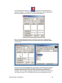
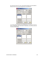
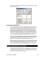
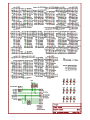
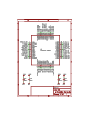
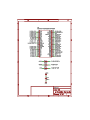
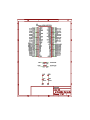
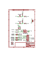
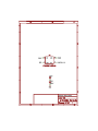
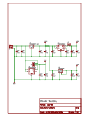
1
XSA-3S1000 Board V1.0
User Manual
How to install, test, and use
your new XSA-3S1000 Board
RELEASE DATE: 6/23/2005
Copyright © 2001-2005 by X Engineering Software Systems Corporation.
All XS-prefix product designations are trademarks of XESS Corp.
All XC-prefix product designations are trademarks of XILINX.
All rights reserved. No part of this publication may be reproduced, stored in a retrieval
system, or transmitted, in any form or by any means, electronic, mechanical,
photocopying, recording, or otherwise, without the prior written permission of the publisher.
Printed in the United States of America.
XSA-3S1000 BOARD V1.0 USER MANUAL
1
Table of Contents
Table of Contents .............................................................................................2
Preliminaries .....................................................................................................4
Getting Help!.................................................................................................4
Take notice!! .................................................................................................4
Packing List ..................................................................................................5
Installation .........................................................................................................6
Installing the XSTOOLS Utilities and Documentation ................................6
Applying Power to Your XSA-3S1000 Board .............................................6
Using a 5V - 9V DC wall-mount power supply ...........................................6
Powering Through the PS/2 Connector......................................................6
Solderless Protoboard Installation...............................................................7
Connecting a PC to Your XSA-3S1000 Board...........................................8
Connecting a VGA Monitor to Your XSA-3S1000 Board...........................8
Connecting a Mouse or Keyboard to Your XSA-3S1000 Board ...............9
Inserting the XSA-3S1000 Board into an XStend Board ...........................9
Setting the Jumpers on Your XSA-3S1000 Board.....................................9
Testing Your XSA-3S1000 Board ...............................................................9
Setting the XSA-3S1000 Board Clock Oscillator Frequency...................10
Programming ..................................................................................................11
Generating Bitstreams for the FPGA ........................................................11
Downloading Bitstreams into the FPGA and CPLD.................................12
Downloading Using GXSLOAD.................................................................12
Downloading Using Xilinx iMPACT ...........................................................15
Storing Non-Volatile Bitstreams in the Flash ............................................15
Downloading and Uploading Data to the SDRAM ...................................18
XSA-3S1000 BOARD V1.0 USER MANUAL
2
Programmer's Models ....................................................................................20
XSA-3S1000 Board Organization .............................................................20
Programmable logic: FPGA and CPLD ....................................................21
100 MHz Fixed-Frequency Oscillator........................................................22
Synchronous DRAM ..................................................................................23
Flash RAM..................................................................................................23
Seven-Segment LED .................................................................................25
DIP Switches and Pushbuttons.................................................................25
PS/2 Port.....................................................................................................26
VGA Port.....................................................................................................26
Parallel Port ................................................................................................27
XILINX Parallel Cable IV Connector .........................................................30
Prototyping Header ....................................................................................30
XSA-3S1000 Pin Connections.......................................................................32
XSA-3S1000 Schematics...............................................................................33
XSA-3S1000 BOARD V1.0 USER MANUAL
3
1
Preliminaries
Getting Help!
Here are some places to get help if you encounter problems:
If you can't get the XSA-3S1000 Board hardware to work, send an e-mail message
describing your problem to [email protected] or submit a problem report at
http://www.xess.com/help.html. Our web site also has
answers to frequently-asked-questions,
example designs, application notes and tutorials for the XS Boards,
a place to sign-up for our email forum where you can post questions to other XS
Board users.
If you can't get your XILINX WebPACK software tools installed properly, send an email message describing your problem to [email protected] or check their web site
at http://www.xilinx.com/support/support.htm.
If you need help using the WebPACK software to create designs for your XSA3S1000 Board, then check out this tutorial.
Take notice!!
The XSA-3S1000 is not 5V-tolerant. Do not connect 5V logic signals to the
prototyping header. Do not insert your XSA-3S1000 Board into an XST-1 or XST-2.x
XStend Board. These versions of the XStend Boards contain some 5V logic.
The XSA-3S1000 Board requires an external power supply to operate! It does not
draw power through the downloading cable from the PC parallel port.
If you are connecting a 5V - 9V DC power supply to your XSA-3S1000 Board, please
make sure the center terminal of the plug is positive and the outer sleeve is negative.
Do not power your XSA-3S1000 Board with a battery! This will not provide enough
current to insure reliable operation of the XSA-3S1000 Board.
Even if you have experience with the XILINX software tools, please read this section
on setting the bitstream generation options for the XSA-3S1000 Board.
XSA-3S1000 BOARD V1.0 USER MANUAL
4
Packing List
Here is what you should have received in your package:
an XSA-3S1000 Board;
a 6' cable with a 25-pin male connector on each end;
an XSTOOLS CDROM with software utilities and documentation for using the XSA3S1000 Board.
XSA-3S1000 BOARD V1.0 USER MANUAL
5
2
Installation
Installing the XSTOOLS Utilities and Documentation
XILINX currently provides the WebPACK tools for programming their CPLDs and Spartanseries FPGAs. The XESS CDROM contains a version of WebPACK that will generate
bitstream configuration files compatible with your XSA-3S1000 Board. You can also
download the most current version of the WebPACK tools from the XILINX website.
In addition, XESS Corp. provides the XSTOOLS utilities for interfacing a PC to your XSA3S1000 Board. These utilities should be installed automatically when you insert the
XSTOOLS CDROM into your CDROM drive. If not, then manually run the SETUP.EXE
installation program on the CDROM.
Applying Power to Your XSA-3S1000 Board
You can use your XSA-3S1000 Board in three ways, distinguished by the method you use
to apply power to the board. Only use one of these methods to power your XSA3S1000 Board! Supplying power from multiple sources can damage the board and/or
power supplies.
Using a 5V - 9V DC wall-mount power supply
You can use your XSA-3S1000 Board all by itself to experiment with logic designs. Just
place the XSA-3S1000 Board on a non-conducting surface as shown in Figure 1. Then
apply power to the XSA-3S1000 Board from a DC wall-mount power supply with a 2.1 mm
female, center-positive plug and a voltage in the range 5V – 9V. (See Figure 2 for the
location of the 5V – 9V DC power jack on your XSA-3S1000 Board.) The shunt on jumper
J7 should be in the “9V” position. The on-board voltage regulation circuitry will create the
voltages required by the rest of the XSA-3S1000 Board circuitry. Be careful!! The
voltage regulator on the XSA-3S1000 Board can become hot. To reduce the
power dissipation in the regulator and keep it cool, use a power supply with a voltage near
5V. You can also attach a heat sink to the regulator if necessary.
Powering Through the PS/2 Connector
You can use your XSA-3S1000 Board with a laptop PC by connecting a PS/2 male-tomale cable between the PS/2 ports of the laptop and the board. The shunt on jumper J7
should be in the “PS/2” position. The on-board voltage regulation circuitry will create the
voltages required by the rest of the XSA-3S1000 Board circuitry. Many PS/2 ports
cannot supply more than 0.5A so large, high-frequency FPGA designs may not
work when using this power source!
XSA-3S1000 BOARD V1.0 USER MANUAL
6
Solderless Protoboard Installation
The two rows of pins from your XSA-3S1000 Board can be plugged into a solderless
protoboard with holes spaced at 0.1" intervals. (One of the A.C.E. protoboards from 3M is
a good choice.) Once plugged in, many of the pins of the FPGA are accessible to other
circuits on the protoboard. (The labels printed next to the rows of pins on your XSA3S1000 Board correspond to the pin numbers of the FPGA.) Power can still be supplied
to your XSA-3S1000 Board though the 5V – 9V DC jack, or power can be applied directly
through several pins on the underside of the board. Just connect +5V, +3.3V, +2.5V and
ground to the pins of your XSA-3S1000 Board listed in Table 1. (Remove the shunt on
jumper J2 if you supply +2.5V from an external source.)
• Table 1: Power supply pins for the XSA-3S1000 Board.
Voltage
Pin
Note
+5V
2
This pin is labeled “+5V”.
+3.3V
54
This pin is labeled “+3.3V”.
+2.5V
22
This pin is labeled “+2.5V”.
GND
52
This pin is labeled “GND”.
Parallel Port
5V – 9V
PS/2
VGA
• Figure 1: External connections to the XSA-3S1000 Board.
XSA-3S1000 BOARD V1.0 USER MANUAL
7
Parallel Port
Parallel Cable IV Connector
5V – 9V DC
100 MHz Oscillator
LED Digit
CPLD
Flash
FPGA
DIP Switches
SDRAM
pushbuttons
PS/2 Port
VGA Port
• Figure 2: Arrangement of components on the XSA-3S1000 Board.
Connecting a PC to Your XSA-3S1000 Board
The 6' DB25 male-to-male cable included with your XSA-3S1000 Board connects it to a
PC. One end of the cable attaches to the parallel port on the PC and the other connects to
the female DB-25 connector at the top of the XSA-3S1000 Board as shown in Figure 1.
Connecting a VGA Monitor to Your XSA-3S1000 Board
You can display images with up to 512 colors on a VGA monitor by connecting it to the
VGA port at the bottom of your XSA-3S1000 Board (see Figure 1). You will have to create
a VGA display circuit for your XSA-3S1000 Board to actually display an image. See this
section for details on the VGA port circuitry and an example of a VGA display circuit.
XSA-3S1000 BOARD V1.0 USER MANUAL
8
Connecting a Mouse or Keyboard to Your XSA-3S1000 Board
You can accept inputs from a keyboard or mouse by connecting it to the PS/2 port at the
bottom of your XSA-3S1000 Board (see Figure 1). You will have to create a keyboard or
mouse interface circuit to actually receive information on keystrokes or mouse
movements. See this section for details on the PS/2 port circuitry and an example of a
keyboard interface.
Inserting the XSA-3S1000 Board into an XStend Board
Do not insert an XSA-3S1000 Board into an XST-1 or XST-2.x XStend Board. The
XSA-3S1000 Board is not compatible with the voltages on these versions of the XStend
Board. An XST-3.0 XStend Board will be available in 2005.
Setting the Jumpers on Your XSA-3S1000 Board
The default jumper settings shown in Table 2 configure your XSA-3S1000 Board for use in
a logic design environment. You will need to change the jumper settings only if you are:
downloading FPGA bitstreams to your XSA-3S1000 Board using the XILINX iMPACT
software;
changing the power sources for the XSA-3S1000 supply voltages.
• Table 2: Jumper settings for XSA-3S1000 Boards.
Jumper
J2
J7
Setting
Purpose
On
(default)
A shunt should be installed if the +2.5V supply voltage is derived from the +3.3V supply.
Off
The shunt should be removed if the +2.5V supply voltage is applied from an external source through
pin 22 of the XSA-3S1000 Board (labeled “+2.5V” at the lower right-hand corner of the board).
1-2
(9V)
The shunt should be installed on pins 1 and 2 if the board supply voltages are derived from the an
external 5V – 9V DC supply.
2-3
The shunt should be installed on pins 2 and 3 if the board supply voltages are derived from the +5V
supply applied through the PS/2 keyboard/mouse connector (J4).
(PS/2)
J9
J10
1-2 (XI)
The shunt should be installed on pins 1 and 2 (XI) if the XSA-3S1000 Board is to be downloaded using
the XILINX iMPACT software.
2-3 (XS)
(default)
The shunt should be installed on pins 2 and 3 (XS) if the XSA-3S1000 Board is to be downloaded
using the XESS GXSLOAD software.
N/A
This is a header that provides access to the +5V and GND references on the board. No shunt should
be placed on this header.
Testing Your XSA-3S1000 Board
Once your XSA-3S1000 Board is installed and the jumpers are in their default
configuration, you can test the board using the GUI-based GXSTEST utility as follows.
XSA-3S1000 BOARD V1.0 USER MANUAL
9
You start GXSTEST by clicking on the
icon placed on the desktop during the
XSTOOLS installation. This brings up the window shown below.
Next you select the parallel port that your XSA-3S1000 Board is connected to from the
Port pulldown list. GXSTEST starts with parallel port LPT1 as the default, but you can
also select LPT2 or LPT3 depending upon the configuration of your PC.
After selecting the parallel port, pick the XSA-3S1000 item in the Board Type pulldown list.
Then click on the TEST button to start the testing procedure. GXSTEST will configure the
FPGA to perform a test procedure on your XSA-3S1000 Board. Within thirty seconds you
will see a O displayed on the LED digit if the test completes successfully. Otherwise an E
will be displayed if the test fails. A status window will also appear on your PC screen
informing you of the success or failure of the test.
If your XSA-3S1000 Board fails the test, you will be shown a checklist of common causes
for failure. If none of these causes applies to your situation, then try some of the solutions
listed in the XSTOOLS\README.TXT file. If you cannot get your board to pass the test
even after taking these steps, then contact XESS Corp for further assistance.
As a result of testing the XSA-3S1000 Board, the CPLD is programmed with the standard
parallel port interface found in the XSTOOLS\XSA\3S1000\dwnldpar.svf bitstream file.
This is the interface that should be loaded into the CPLD when you want to use it with the
GXSLOAD utility.
Setting the XSA-3S1000 Board Clock Oscillator Frequency
Unlike previous versions of the XSA Board, your XSA-3S1000 Board has a fixedfrequency oscillator of 100 MHz. The GXSSETCLK utility cannot be used to change the
frequency of the clock sent to the FPGA and CPLD. You can lower the clock frequency by
placing a clock-divider circuit in the FPGA or CPLD. See the section on the XSA-3S1000
Board clock circuitry for more details.
XSA-3S1000 BOARD V1.0 USER MANUAL
10
3
Programming
This section will show you how to download logic designs into the FPGA and CPLD of
your XSA-3S1000 Board and how to download and upload data to and from the SDRAM
and Flash devices on the board.
Generating Bitstreams for the FPGA
Before downloading a bitstream to the FPGA on your XSA-3S1000 Board, you will use the
XILINX development software to generate the .BIT file. Steps for doing this are given in
the XILINX documentation, but there is one detail that is specific to your board. The
Spartan3 FPGA has relatively low-impedance, internal pullup and pulldown resistors on its
pins that become active after the FPGA is configured. These resistors can overpower the
4.7KΩ external pullup and pulldown resistors on the board and prevent it from functioning
correctly. Therefore, you have to set the bitstream generation options to disable these
internal resistors. This is done by right-clicking on the Generate Programming File item in
the Processes pane and selecting Properties… from the pop-up menu.
XSA-3S1000 BOARD V1.0 USER MANUAL
11
Then select the Configuration Options tab in the Process Properties window and change
all the pin settings to float. Then click on the OK button. The internal pullup and pulldown
resistors will now be disabled in the bitstream generated for this project.
Downloading Bitstreams into the FPGA and CPLD
Downloading Using GXSLOAD
As you develop and test a logic design, you will usually connect the XSA-3S1000 Board to
the parallel port of a PC and download the configuration bitstream each time you make
changes. You can download a bitstream into your XSA-3S1000 Board using the
GXSLOAD utility.
XSA-3S1000 BOARD V1.0 USER MANUAL
12
You start GXSLOAD by clicking on the
icon placed on the desktop during the
XSTOOLS installation. This brings up the window shown below. Select the XSA-3S1000
Board and the parallel port to which it is connected as indicated below.
Now you can download bitstream files to the FPGA or CPLD simply by dragging them
from their folder and dropping them into the FPGA/CPLD pane of the GXSLOAD window
as shown below.
Once you drop the file, the highlighted file name appears in the FPGA/CPLD pane and the
Load button in the GXSLOAD window is enabled. Clicking on the Load button will begin
sending the bitstream in the file to the XSA-3S1000 Board through the parallel port
connection. .BIT files contain configuration bitstreams that are loaded into the FPGA while
.SVF files will go to the CPLD. GXSLOAD will reject any non-downloadable files (ones
XSA-3S1000 BOARD V1.0 USER MANUAL
13
with a suffix other than .BIT or .SVF). During the downloading process, GXSLOAD will
display the name of the file and the progress of the current download.
You can drag & drop multiple files into the FPGA/CPLD area. Clicking your mouse on a
filename will highlight the name and select it for downloading. Only one file at a time can
be selected for downloading.
XSA-3S1000 BOARD V1.0 USER MANUAL
14
Double-clicking the highlighted file will deselect it so no file will be downloaded. Doing this
disables the Load button.
Downloading Using Xilinx iMPACT
You can use the Xilinx iMPACT software to download bitstreams to the XSA-3S1000
Board. The iMPACT programming tool downloads bitstreams through the JTAG interface
of the FPGA so we need to change the parallel port interface by reprogramming the
CPLD. Drag & drop the p3jtag.svf file from the XSTOOLS\XSA\3S1000 folder into the
FPGA/CPLD pane of the GXSLOAD window. Then click on the Load button and the
CPLD will be reprogrammed in less than a minute. Then move the shunt on jumper J9
from the XS to the XI position. At this point you can start iMPACT and it will believe it is
connected to the XSA-3S1000 Board through a Xilinx Parallel Cable III in boundary-scan
mode. Follow the instructions for iMPACT to download bitstreams to the FPGA.
You can also use a Xilinx Parallel Cable IV with the XSA-3S1000 Board by downloading
the XSTOOLS\XSA\3S1000\p4jtag.svf file into the CPLD. Then disconnect the XESS
downloading cable and connect the Xilinx Parallel Cable IV to the X4 connector. Now
start iMPACT to download bitstreams to the FPGA in boundary-scan mode.
Note that the CPLD only needs to be reprogrammed once to support iMPACT because it
retains its configuration even when power is removed from the board. (If you want to go
back to using the GXSLOAD programming utility, just must move the shunt on J9 back to
the XS position and download the XSTOOLS\XSA\dwnldpar.svf file into the CPLD.)
Storing Non-Volatile Bitstreams in the Flash
The FPGA on the XSA-3S1000 Board stores its configuration in an on-chip SRAM which
is erased whenever power is removed. Once your design is finished, you may want to
store the bitstream in the 16 Mbit Flash device on the XSA-3S1000 Board from which the
FPGA will be configured each time power is applied.
XSA-3S1000 BOARD V1.0 USER MANUAL
15
The Flash is partitioned into four quadrants, each of which can hold a bitstream for the
FPGA. Before a bitstream can be downloaded into a quadrant of the Flash, the .BIT file
must be converted into an .EXO or .MCS format using one of the following commands:
Quadrant
Address Range
0
0x000000 – 0x07FFFF
1
Conversion Command
DIP Switch Setting
SW1-1
SW1-2
promgen –u 0 file.bit –p exo -w
promgen –u 0 file.bit –p mcs –w
ON
ON
0x080000 – 0x0FFFFF
promgen –u 80000 file.bit –p exo -w
promgen –u 80000 file.bit –p mcs –w
ON
OFF
2
0x100000 – 0x17FFFF
promgen –u 100000 file.bit –p exo -w
promgen –u 100000 file.bit –p mcs –w
OFF
ON
3
0x180000 – 0x1FFFFF
promgen –u 180000 file.bit –p exo -w
promgen –u 180000 file.bit –p mcs -w
OFF
OFF
In the commands shown above, the bitstream in file.bit is transformed into an .EXO or
.MCS formatted file starting at the first address in each quadrant and proceeding upward.
The .EXO or .MCS file is downloaded into the Flash device by dragging it into the
Flash/EEPROM pane and clicking on the Load button. This activates the following
sequence of steps:
1. The FPGA and CPLD on the XSA-3S1000 Board are reprogrammed to create an
interface between the Flash device and the PC parallel port.
2. The entire Flash device is erased.
3. The contents of the .EXO or .MCS file are downloaded into the Flash through the
parallel port.
4. The CPLD is reprogrammed with a circuit that configures the FPGA with the
contents of the Flash whenever power is applied to the XSA-3S1000 Board.
(This configuration loader is stored in the XSTOOLS\XSA\3S1000\fcnfg.svf file.)
Once the Flash download is complete, you must set the DIP switches to select the Flash
quadrant containing the FPGA bitstream (see the switch settings in the table above). The
FPGA will be configured with the bitstream in that quadrant whenever power is applied to
the board. You can download multiple bitstreams to the Flash and use the switches to
select the one to be loaded into the FPGA on power-up.
Multiple files can be stored in the Flash device just by dragging them into the
Flash/EEPROM area, highlighting the files to be downloaded and clicking the Load button.
(Note that anything previously stored in the Flash will be erased by each new download.)
This is useful if you need to store information in the Flash in addition to the FPGA
bitstream. Files are selected and de-selected for downloading just by clicking on their
names in the Flash/EEPROM area. The address ranges of the data in each file
should not overlap or this will corrupt the data stored in the Flash device!
You can also examine the contents of the Flash device by uploading it to the PC. To
upload data from an address range in the Flash, type the upper and lower bounds of the
range into the High Address and Low Address fields located below the Flash/EEPROM
pane, and select the format for the uploaded data from the Upload Format pulldown list.
XSA-3S1000 BOARD V1.0 USER MANUAL
16
Then click on the file icon and drag & drop it into any folder. This activates the following
sequence of steps:
1. The CPLD and FPGA on the XSA-3S1000 Board are reprogrammed to create an
interface between the Flash device and the PC parallel port.
2. The Flash data between the high and low addresses (inclusive) is uploaded
through the parallel port.
3. The uploaded data is stored in a file named FLSHUPLD with an extension that
reflects the file format.
The uploaded data can be stored in the following formats:
MCS: Intel hexadecimal file format. This is the same format generated by the promgen
utility with the –p mcs option.
HEX: Identical to MCS format.
EXO-16: Motorola S-record format with 16-bit addresses (suitable for 64 KByte uploads
only).
EXO-24: Motorola S-record format with 24-bit addresses. This is the same format
generated by the promgen utility with the –p exo option.
EXO-32: Motorola S-record format with 32-bit addresses.
XESS-16: XESS hexadecimal format with 16-bit addresses. (This is a simplified file
format that does not use checksums.)
XESS-24: XESS hexadecimal format with 24-bit addresses.
XESS-32: XESS hexadecimal format with 32-bit addresses.
XSA-3S1000 BOARD V1.0 USER MANUAL
17
After the data is uploaded from the Flash, the default parallel port interface remains in the
CPLD. You will need to reprogram the CPLD with the configuration loader bitstream in
XSTOOLS\XSA\3S1000\fcnfg.svf if you want the FPGA to be configured from Flash
whenever power is applied.
Downloading and Uploading Data to the SDRAM
The XSA-3S1000 Board contains a 256 Mbit, synchronous DRAM (16M x 16 SDRAM)
whose contents can be downloaded and uploaded by GXSLOAD. This is useful for
initializing the SDRAM with data for use by the FPGA and then reading the SDRAM
contents after the FPGA has operated upon it. The SDRAM is loaded with data by
dragging & dropping one or more .EXO, .MCS, .HEX, and/or .XES files into the RAM pane
of the GXSLOAD window and then clicking on the Load button. This activates the
following sequence of steps:
1. The FPGA is reprogrammed to create an interface between the SDRAM and the
PC parallel port. (This interface is stored in the
XSTOOLS\XSA\3S1000\ramintfc.bit bitstream file. The CPLD must have
previously been loaded with the dwnldpar.svf file found in the same
folder.)
2.
The contents of the .EXO, .MCS, .HEX or .XES files are downloaded into the
SDRAM through the parallel port. The data in the files will overwrite each
other if their address ranges overlap.
3. If any file is highlighted in the FPGA/CPLD pane, then this bitstream is loaded into
the FPGA or CPLD on the XSA-3S1000 Board. Otherwise the FPGA remains
configured as an interface between the PC and the SDRAM.
You can also examine the contents of the SDRAM device by uploading it to the PC. To
upload data from an address range in the SDRAM, type the upper and lower bounds of
the range into the High Address and Low Address fields below the RAM pane, and select
the format for the uploaded data from the Upload Format pulldown list. Then click on the
file icon and drag & drop it into any folder. This activates the following sequence of steps:
1. The FPGA is reprogrammed to create an interface between the SDRAM device
and the PC parallel port.
2. The SDRAM data between the high and low addresses (inclusive) is uploaded
through the parallel port.
3. The uploaded data is stored in a file named RAMUPLD with an extension that
reflects the file format.
XSA-3S1000 BOARD V1.0 USER MANUAL
18
The 16-bit data words in the SDRAM are mapped into the eight-bit data format of the
.HEX, .MCS, .EXO and .XES files using a Big Endian style. That is, the 16-bit word at
location N in the SDRAM is stored in the eight-bit file with the upper eight bits at address
2N and the lower eight bits at address 2N+1. This byte-ordering applies for both RAM
uploads and downloads.
XSA-3S1000 BOARD V1.0 USER MANUAL
19
4
Programmer's
Models
This section describes the various sections of the XSA-3S1000 Board and shows how the
I/O of the FPGA and CPLD are connected to the rest of the circuitry. The schematics
which follow are less detailed so as to simplify the descriptions. For more information, you
can find a table of FPGA and CPLD pin connections and detailed schematics at the end of
this manual.
XSA-3S1000 Board Organization
The XSA-3S1000 Board contains the following components:
FPGA: This is the main repository of programmable logic on the XSA-3S1000 Board.
CPLD: This manages the interface between the PC parallel port and the rest of the XSA3S1000 Board. It can also configure the FPGA with a bitstream from Flash.
Oscillator: A fixed-frequency oscillator generates the master clock for the XSA-3S1000
Board.
SDRAM: A 256 Mbit SDRAM provides volatile data storage accessible by the FPGA.
Flash: A 16 Mbit Flash device provides non-volatile storage for data and FPGA
configuration bitstreams.
LED: A seven-segment LED allows visible feedback as the XSA-3S1000 Board operates.
DIP switch: A four-position DIP switch passes settings to the XSA-3S1000 Board and
controls the upper address bits of the Flash device.
Pushbuttons: Two pushbuttons send momentary contact information to the FPGA.
PS/2 Port: A keyboard or mouse can interface to the XSA-3S1000 Board through this port.
VGA Port: The XSA-3S1000 Board can send signals to display 512-color graphics on a
VGA monitor through this port.
Parallel Port: This is the main interface for passing configuration bitstreams and data to
and from the XSA-3S1000 Board.
XSA-3S1000 BOARD V1.0 USER MANUAL
20
Prototyping Header: Many of the FPGA I/O pins are connected to the 84 pins on the
bottom of the XSA-3S1000 Board that are meant to mate with solderless breadboards
or an XST-3 Board.
RESET#
BYTE#
WE#
OE#
A19
CE#
A18
A17-A0
D15-D8
D7-D0
FLASH
Parallel Port
2 - PPD0
CPLD
FPGA
D15 - D0
3 - PPD1
SDRAM
BA1 - BA0, A12 - A0
4 - PPD2
5 - PPD3
RAS, CAS, CS#, WE#
6 - PPD4
A17 - A0
7 - PPD5
8 - PPD6
DQMH
DQML
D15 - D8
9 - PPD7
17 - PPC3
TDI
16 - PPC2
TMS
14 - PPC1
TCK
11 - PPS7
TDO
D7 - D0
CKE
D7-D0
CCLK
PROGRAM#
CLK
GCLK
INIT#
PS/2 Port
CS#
12 - PPS5
CLK
WR#
13 - PPS4
DATA
BSY/DOUT
15 - PPS3
DONE
TCK
VGA Connector
TMS
GCLK
OSC
TDI
TDO
GCLK
GCLK
RED2 - RED0
GREEN2 - GREEN0
BLUE2 - BLUE0
HSYNC#
1 - PPC0
VSYNC#
10 - PPS6
• Figure 3: XSA-3S1000 Board programmer’s model.
Programmable logic: FPGA and CPLD
The XSA-3S1000 Board contains two programmable logic chips:
A 1,000,000-gate XILINX Spartan3 FPGA in a 256-pin BGA package (XC3S10004FT256) is the main repository of programmable logic on the XSA-3S1000 Board.
A XILINX XC9500XL CPLD (XC9572XL-10VQ64) is used to manage the
configuration of the FPGA via the parallel port. In stand-alone mode, the CPLD also
configures the FPGA with a bitstream from the Flash RAM.
XSA-3S1000 BOARD V1.0 USER MANUAL
21
100 MHz Fixed-Frequency Oscillator
An oscillator provides a fixed, 100 MHz clock signal to a dedicated clock input of the
CPLD. From this clock, the CPLD generates two clock signals, CLKA and CLKB, that go
to dedicated clock inputs of the FPGA. This allows the CPLD to control the FPGA clocks.
By default, the CPLD outputs 100 MHz and 50 MHz clocks on CLKA and CLKB,
respectively. The clock-divider circuit in the CPLD can be reprogrammed to send lowerfrequency clocks to the FPGA if desired.
The CLKB signal also exits through a pin on the prototyping header, so it can be used as a
clock for an external system connected to the XSA-3S1000 Board. Or the external system
can send a clock directly to the FPGA through the dedicated CLKC pin of the prototyping
header.
CLKA
100 Mhz
Oscillator
MASTER-CLK
CPLD
CLKB
GCLK
GCLK
FPGA
CLKB
CLKC
XSA-3S1000 BOARD V1.0 USER MANUAL
GCLK
22
Synchronous DRAM
The XSA-3S1000 Board incorporates a 16M x 16 SDRAM (K4S561632ETC75) that
connects solely to the FPGA as shown below. Note that the clock signal is re-routed back
to a dedicated clock input of the FPGA to compensate for clock delays to the SDRAM,
thus allowing synchronization of the FPGA’s internal operations with the SDRAM
operations.
This application note describes an SDRAM controller that makes the SDRAM appear like
a simple static RAM to the rest of the circuitry in the FPGA.
FPGA
SDRAM
D15 - D0
UDQM
LDQM
A12 - A0
BA1 - BA0
RAS#
CAS#
CS#
WE#
CKE
CLK
GCLK
Flash RAM
The CPLD and FPGA connect to a 16 Mbit Flash RAM (S29AL016M10TAI020) that
operates in either byte mode (2M x 8) or word mode (1M x 16). The CPLD uses the byte
mode as it only has access to the lower eight bits of the Flash data bus, while the FPGA
connects to the entire 16-bit data bus and can select either mode using the BYTE# control
line.
The FPGA has access to the entire Flash address bus so it can read or write any location.
For this reason, the FPGA is used to pass data between the parallel port and the Flash
when GXSLOAD downloads/uploads files to/from the Flash. The CPLD, however, is not
connected to the upper two address lines so it can only access a quadrant of the Flash.
The quadrant is selected by two DIP switches connected to the upper address lines. On
power-up in stand-alone mode, the CPLD configures the FPGA with a bitstream retrieved
XSA-3S1000 BOARD V1.0 USER MANUAL
23
from the selected quadrant, so the DIP switches can be used to select between four
separate bitstreams stored in the Flash. (See the application note on the XSA Board Flash
configuration circuit for more details on this.)
After power-up, any application circuit loaded into the FPGA can read and/or write the
Flash. To avoid contention, the CPLD is programmed to release control of all Flash
address/data/control lines whenever the FPGA lowers the Flash CE# line. When the
Flash is disabled by raising CE#, the I/O lines connected to the Flash are available for
general-purpose communication between the FPGA and the CPLD.
CE#
OE#
WE#
A0
A1
A2
A3
A4
A5
A6
A7
A8
A9
A10
A11
A12
A13
A14
A15
A16
A17
A18
A19
D0
D1
D2
D3
D4
D5
D6
D7
D8
D9
D10
D11
D12
D13
D14
D15
RESET#
BYTE#
FLASH
CPLD
FPGA
SW1-2
SW1-1
+3.3V
XSA-3S1000 BOARD V1.0 USER MANUAL
24
Seven-Segment LED
The XSA-3S1000 Board has a 7-segment LED digit for use by the FPGA or the CPLD.
Segments of the LED glow when a logic-high level is applied to them.
The LED shares the same eight-bit data bus that interconnects the CPLD, the FPGA
configuration port and the lower-byte of the Flash RAM data bus. The connections
between the LED segments and the data bus are shown below. (We use two distinct
labelings of the LED segments in our documentation and design examples, so we show
the connections for both.)
FPGA-DIN-D0
FPGA-D1
FPGA-D2
FPGA-D3
FPGA-D4
FPGA-D5
FPGA-D6
FPGA-D7
C
DP
B
A
F
G
E
D
A
F
G
B
C
E
D
DP
FPGA-DIN-D0
FPGA-D1
FPGA-D2
FPGA-D3
FPGA-D4
FPGA-D5
FPGA-D6
FPGA-D7
S1
DP
S4
S6
S5
S3
S2
S0
S6
S5
S3
S4
S1
S2
S0
DP
DIP Switches and Pushbuttons
Four DIP switches are attached to the FPGA. When closed (ON), each switch pulls the
connected pin of the FPGA to ground. The pin is pulled high through a resistor when the
switch is open (OFF).
Two of the DIP switches also connect to the upper two bits of the Flash address bus.
These DIP switches are used to select the Flash quadrant holding a bitstream that will be
loaded into the FPGA by the CPLD on power-up.
XSA-3S1000 BOARD V1.0 USER MANUAL
25
The FPGA also connects to two pushbuttons. Each pushbutton applies a low level to its
FPGA pin when pressed and a resistor pulls the pin to a high level when the pushbutton is
released.
Small resistors are placed in series between the FPGA and the switches and pushbuttons
to prevent damage if the FPGA tries to drive a pin that is being pulled low.
+3.3V
FLASH A19
FLASH A18
FPGA
SW1-1
SW1-2
SW1-3
SW1-4
SW2
SW3
PS/2 Port
A PS/2 port provides the FPGA with an interface to either a keyboard or a mouse. The
FPGA receives two signals from the PS/2 interface: a clock signal and a serial data stream
that is synchronized with the falling edge of the clock. (For more details on using the PS/2
port and a simple circuit for receiving keystroke information from a keyboard, see this
application note.)
+3.3V
FPGA
CLK
DATA
VGA Port
The FPGA can generate a video signal for display on a VGA monitor. The FPGA outputs
three bits each of red, green, and blue color information to a simple resistor-ladder DAC.
This provides a palette of 23 x 23 x 23 = 512 colors. The outputs of the DAC are sent to the
XSA-3S1000 BOARD V1.0 USER MANUAL
26
RGB inputs of a VGA monitor. The FPGA also generates the horizontal and vertical sync
pulses (HSYNC#, VSYNC#). ( See this application note for more details on a simple
circuit for generating VGA signals that displays an image stored in SDRAM.)
FPGA
VSYNC#
HSYNC#
RED0
RED1
RED2
GREEN0
GREEN1
GREEN2
BLUE0
BLUE1
BLUE2
Parallel Port
The parallel port is the main interface for communicating between the XSA-3S1000 Board
and a PC. Control line C0 and status line S6 connect directly to the FPGA and can be
used for bidirectional communication between the FPGA and PC. The CPLD handles the
fifteen remaining active lines of the parallel port as follows.
Three of the parallel port control lines, C1–C3, connect to the JTAG pins through which
the CPLD is programmed. The C1 control line clocks configuration data presented on the
C3 line into the CPLD while the C2 signal steers the actions of the CPLD programming
state machine. Meanwhile, information from the CPLD returns to the PC through status
line S7.
The eight data lines, D0–D7, and the remaining three status lines, S3–S5, connect to
general-purpose pins of the CPLD. The CPLD can be programmed to act as an interface
between the FPGA and the parallel port. The CPLD connects to the FPGA configuration
pins so it can pass bitstreams from the parallel port to the FPGA. The actual configuration
data is presented to the FPGA on the same 8-bit bus that also connects to the Flash and
seven-segment LED. The CPLD also drives the configuration pins (CCLK, PROGRAM#,
CS#, and WR#) that sequence the loading of a bitstream into the FPGA. The CPLD can
monitor the status of the bitstream download through the INIT#, DONE, and BSY/DOUT
pins.
The CPLD also has access to the FPGA’s JTAG pins: TCK, TMS, TDI, and TDO. The
TMS, TDI, and TDO pins share the connections with the BSY/DOUT, CS#, and WR# pins.
The CPLD can be programmed with an interface that allows configuration of the FPGA
through the JTAG pins using the XILINX iMPACT software (see this application note for
more details). Jumper J9 allows the connection of status pin S7 to the general-purpose
CPLD pin that also drives status pin S5. This is required by the iMPACT software so it can
check for the presence of the downloading cable.
XSA-3S1000 BOARD V1.0 USER MANUAL
27
FLASH
Parallel Port
2 - PPD0
CPLD
FPGA
3 - PPD1
4 - PPD2
D7 - D0
5 - PPD3
D7-D0
6 - PPD4
CCLK
7 - PPD5
PROGRAM#
8 - PPD6
INIT#
CS#
9 - PPD7
17 - PPC3
16 - PPC2
14 - PPC1
11 - PPS7
TDI
WR#
TMS
BSY/DOUT
TCK
DONE
TDO
TCK
12 - PPS5
TMS
13 - PPS4
TDI
15 - PPS3
TDO
1 - PPC0
10 - PPS6
After the FPGA is configured with a bitstream and the DONE pin goes high, the CPLD
switches into a mode that connects the parallel port data and status pins to the FPGA.
This lets the PC pass data to the FPGA over the parallel port data lines while receiving
data from the FPGA over the status lines. The active connections between the FPGA,
CPLD and the parallel port after configuration are shown below.
XSA-3S1000 BOARD V1.0 USER MANUAL
28
CE#
OE#
WE#
A0
A1
A2
A3
A4
A5
A6
A7
A8
A9
A10
A11
A12
A13
A14
A15
A16
A17
A18
A19
D0
D1
D2
D3
D4
D5
D6
D7
D8
D9
D10
D11
D12
D13
D14
D15
RESET#
BYTE#
FLASH
CPLD
FPGA
D7
D6
D5
D4
D3
D2
D1
D0
S5
S4
S3
SW1-2
SW1-1
+3.3V
The FPGA sends data to the PC by driving logic levels onto the A0, A1 and A2 Flash
address lines which pass through the CPLD and onto the parallel port status lines S3, S4
and S5, respectively. Conversely, the PC sends data to the FPGA on parallel port data
lines D7–D0 and the data passes through the CPLD and ends up on the A15–A8 Flash
address lines, respectively. The FPGA should never drive A15–A8 unless it is accessing
the Flash, otherwise the CPLD and/or FPGA could be damaged. The CPLD can sense
when the FPGA lowers the Flash CE# and it will release the Flash address lines so the
FPGA can drive them without contention.
The CPLD also drives the decimal-point of the LED display (connected to Flash data line
D1) to give a visual indication when the FPGA is configured with a valid bitstream. Unless
it is accessing the Flash RAM, the FPGA should never drive Flash data line D1 to a low
logic level or it may damage itself or the CPLD. But when the FPGA lowers the Flash
CE#, the CPLD will stop driving the LED decimal-point to allow the FPGA access to data
line D1 of the Flash.
For more details on how the CPLD manages the interface between the parallel port and
the FPGA both before and after device configuration, see this application note.
XSA-3S1000 BOARD V1.0 USER MANUAL
29
XILINX Parallel Cable IV Connector
The XSA-3S1000 Board has a connector (X4) for attaching a XILINX Parallel Cable IV.
The connections between the Parallel Cable IV and the XSA-3S1000 Board are shown
below.
You will need to reprogram the CPLD on the XSA-3S1000 Board with the
XSTOOLS\XSA\3S1000\p4jtag.svf file before you can use the Parallel Cable IV. Then
disconnect the XESS downloading cable and connect the Parallel Cable IV to the X4
connector. You should never simultaneously attach a Parallel Cable IV and the
XESS parallel port downloading cable! After connecting the Parallel Cable IV, you
can use iMPACT to download bitstreams to the FPGA in boundary-scan mode.
Prototyping Header
The pins of the FPGA are accessible through the 84-pin prototyping header on the
underside of the XSA-3S1000 Board. Pin 1 of the header (denoted by a square pad) is
located in the middle of the left-hand edge of the board and the remaining 83 pins are
arranged counter-clockwise around the periphery. The physical dimensions of the
prototyping header and the pin arrangement are shown below.
XSA-3S1000 BOARD V1.0 USER MANUAL
30
1.75"
64
63
0.1"
84
1
21
4.1"
22
A subset of the FPGA pins connects to the prototyping header. These pins are not
connected to any of the other components on the XSA-3S1000 Board so they are
completely free to use for I/O operations with external systems without any restrictions.
The number of the FPGA pin connected to a given header pin is printed next to the header
pin on the board. This makes it easier to find a given FPGA pin when you want to connect
it to an external system.
XSA-3S1000 BOARD V1.0 USER MANUAL
31
A
XSA-3S1000 Pin
Connections
The following tables list the pin numbers of the FPGA and CPLD along with the pin names
of the other chips that they connect to on the XSA-3S1000 Board.
XSA-3S1000 BOARD V1.0 USER MANUAL
32
+1.2V
+2.5V
+3.3V
+5V
CLKA
CLKB
CLKC
CPLD-TDO
FLASH-A0
FLASH-A1
FLASH-A2
FLASH-A3
FLASH-A4
FLASH-A5
FLASH-A6
FLASH-A7
FLASH-A8
FLASH-A9
FLASH-A10
FLASH-A11
FLASH-A12
FLASH-A13
FLASH-A14
FLASH-A15
FLASH-A16
FLASH-A17
FLASH-A18
FLASH-A19
FLASH-BYTE#
FLASH-CE#
FLASH-D8
FLASH-D9
FLASH-D10
FLASH-D11
FLASH-D12
FLASH-D13
FLASH-D14
FLASH-D15
FLASH-OE#
FLASH-RDY
FLASH-RESET#
FLASH-WE#
FPGA-CCLK
FPGA-DIN-D0
FPGA-D1
FPGA-D2
FPGA-D3
FPGA-D4
FPGA-D5
FPGA-D6
FPGA-D7
FPGA-DONE
FPGA-INIT#
Net Name
N5
K14
K13
K12
L14
M16
L13
N16
N14
P15
R16
P14
P13
N12
T14
R13
N10
M14
K3
K4
T8
R4
T4
R5
T5
P6
M7
R6
N7
P7
P5
L12
P16
M13
T15
M11
N11
P10
R10
T7
R7
N6
M6
R14
N9
T9
P8
R9
42
52
1
2
4
5
7
9
10
11
6
8
12
64
63
53
62
51
50
49
48
47
46
45
40
39
38
36
35
34
33
32
13
44
60
61
CPLD Pin (U2)
D4,D13,E5,E12,M5,M12,N4,N13
C4,T2,P4,A6,A11,F1,F16,L1,L16,T6,T11
E8,F7,F8,E9,F9,F10,G11,H11,H 3,37,26,55
FPGA Pin (U1)
Parallel
Port
Switch /
Buttons
SW1-2
SW1-1
LED-C (S1)
LED-DP
LED-B (S4)
LED-A (S6)
LED-F (S5)
LED-G (S3)
LED-E (S2)
LED-D (S0)
LEDs
Flash (U3)
DQ0 (29)
DQ1 (31)
DQ2 (33)
DQ3 (35)
DQ4 (38)
DQ5 (40)
DQ6 (42)
DQ7 (44)
Osc (U6)
VCC (4)
A0 (25)
A1 (24)
A2 (23)
A3 (22)
A4 (21)
A5 (20)
A6 (19)
A7 (18)
A8 (8)
A9 (7)
A10 (6)
A11 (5)
A12 (4)
A13 (3)
A14 (2)
A15 (1)
A16 (48)
A17 (17)
A18 (16)
A19 (9)
BYTE# (47)
CE# (26)
DQ8 (30)
DQ9 (32)
DQ10 (34)
DQ11 (36)
DQ12 (39)
DQ13 (41)
DQ14 (43)
DQ15/A-1 (45)
OE# (28)
RY/BY# (15)
RESET# (12)
WE# (11)
VDD (1,3,9,1VCC (37)
SDRAM
(U4)
VGA
Connections Between the FPGA, CPLD and other Components on the XSA-3S1000 Board
PS/2
11
64
22
54
2
Proto. Pin
(J1)
FPGA-PROG#
FPGA-TCK
FPGA-TDI
FPGA-TDI-CS#
FPGA-TDO
FPGA-TDO-WR#
FPGA-TMS
FPGA-TMS-BSY
GND
MASTER-CLK
PP-C0
PP-C1
PP-C2
PP-C3
PP-D0
PP-D1
PP-D2
PP-D3
PP-D4
PP-D5
PP-D6
PP-D7
PP-S3
PP-S4
PP-S5
PP-S6
PP-S7
PROTO1
PROTO3
PROTO4
PROTO5
PROTO6
PROTO7
PROTO8
PROTO9
PROTO10
PROTO12
PROTO13
PROTO14
PROTO18
PROTO19
PROTO20
PROTO21
PROTO23
PROTO24
PROTO25
PROTO26
PROTO27
PROTO28
PROTO29
PROTO31
PROTO32
PROTO33
Net Name
H16
H15
H14
H13
G16
G15
G14
G13
F15
G12
F14
E16
E15
D16
E14
D15
F5
D2
D1
F4
E2
E1
F3
G5
F2
G4
T10
R11
Switch /
Buttons
Flash (U3)
Osc (U6)
Proto. Pin
(J1)
55
16
30
29
28
27
20
31
23
22
19
18
16
24
25
15
17
1
3
4
5
6
7
8
9
10
12
13
14
18
19
20
21
23
24
25
26
27
28
29
31
32
33
17
52
PS/2
59
VGA
30
VSS (6,12,46VSS (27,46) GND(2)
OUT (3)
SDRAM
(U4)
56
GND (U5.4, U5.12)
LEDs
15
C0 (1)
C1 (14)
C2 (16)
C3 (17)
D0 (2)
D1 (3)
D2 (4)
D3 (5)
D4 (6)
D5 (7)
D6 (8)
D7 (9)
S3 (15)
S4 (13)
S5 (12)
S6 (10)
S7 (11)
Parallel
Port
58
57
43
CPLD Pin (U2)
B3
C14
A2
R3
A15
T3
C13
P9
P3,A1,A16,B2,B9,B15,F6,F11,G 14,21,41,54
FPGA Pin (U1)
Connections Between the FPGA, CPLD and other Components on the XSA-3S1000 Board
PROTO34
PROTO35
PROTO36
PROTO37
PROTO38
PROTO39
PROTO40
PROTO41
PROTO42
PROTO43
PROTO44
PROTO45
PROTO46
PROTO47
PROTO48
PROTO49
PROTO50
PROTO51
PROTO53
PROTO56
PROTO57
PROTO58
PROTO59
PROTO60
PROTO61
PROTO62
PROTO63
PROTO65
PROTO66
PROTO67
PROTO68
PROTO69
PROTO70
PROTO71
PROTO72
PROTO73
PROTO74
PROTO75
PROTO76
PROTO77
PROTO78
PROTO79
PROTO80
PROTO81
PROTO82
PROTO83
PROTO84
PS2-CLK
PS2-DATA
SDRAM-A0
SDRAM-A1
SDRAM-A2
SDRAM-A3
Net Name
N15
M15
L15
K15
K16
J13
J14
J16
B16
E13
B5
A4
B4
E6
M10
P11
T12
R12
T13
P12
N2
L5
P1
M4
N3
P2
R1
G3
G2
G1
H4
H3
H1
J1
J2
J3
K1
L2
K5
L3
M1
M2
L4
N1
M3
FPGA Pin (U1)
CPLD Pin (U2)
Parallel
Port
LEDs
Switch /
Buttons
A0 (23)
A1 (24)
A2 (25)
A3 (26)
SDRAM
(U4)
Flash (U3)
Osc (U6)
VGA
Connections Between the FPGA, CPLD and other Components on the XSA-3S1000 Board
CLK (5)
DATA (1)
PS/2
Proto. Pin
(J1)
34
35
36
37
38
39
40
41
42
43
44
45
46
47
48
49
50
51
53
56
57
58
59
60
61
62
63
65
66
67
68
69
70
71
72
73
74
75
76
77
78
79
80
81
82
83
84
SDRAM-A4
SDRAM-A5
SDRAM-A6
SDRAM-A7
SDRAM-A8
SDRAM-A9
SDRAM-A10
SDRAM-A11
SDRAM-A12
SDRAM-BA0
SDRAM-BA1
SDRAM-CAS#
SDRAM-CKE
SDRAM-CLK
SDRAM-CLK
SDRAM-CS#
SDRAM-D0
SDRAM-D1
SDRAM-D2
SDRAM-D3
SDRAM-D4
SDRAM-D5
SDRAM-D6
SDRAM-D7
SDRAM-D8
SDRAM-D9
SDRAM-D10
SDRAM-D11
SDRAM-D12
SDRAM-D13
SDRAM-D14
SDRAM-D15
SDRAM-LDQM
SDRAM-RAS#
SDRAM-UDQM
SDRAM-WE#
SW1-3
SW1-4
SW2
SW3
VGA-BLUE0
VGA-BLUE1
VGA-BLUE2
VGA-GREEN0
VGA-GREEN1
VGA-GREEN2
VGA-RED0
VGA-RED1
VGA-RED2
VGA-HSYNC#
VGA-VSYNC#
Net Name
E3
C1
E4
D3
C2
A3
B6
C5
C6
A7
C7
A10
D7
N8
E10
B8
C15
D12
A14
B13
D11
A12
C11
D10
B11
B12
C12
B14
D14
C16
F12
F13
C10
A9
D9
B10
K2
J4
E11
A13
C9
E7
D5
A8
A5
C3
C8
D6
B1
B7
D8
FPGA Pin (U1)
CPLD Pin (U2)
Parallel
Port
LEDs
SW1-3
SW1-4
SW2
SW3
Switch /
Buttons
CS# (19)
DQ0 (2)
DQ1 (4)
DQ2 (5)
DQ3 (7)
DQ4 (8)
DQ5 (10)
DQ6 (11)
DQ7 (13)
DQ8 (42)
DQ9 (44)
DQ10 (45)
DQ11 (47)
DQ12 (48)
DQ13 (50)
DQ14 (51)
DQ15 (53)
LDQM (15)
RAS# (18)
UDQM (39)
WE# (16)
SDRAM
(U4)
A4 (29)
A5 (30)
A6 (31)
A7 (32)
A8 (33)
A9 (34)
A10 (22)
A11 (35)
A12 (36)
BA0 (20)
BA1 (21)
CAS# (17)
CKE (37)
CLK (38)
Flash (U3)
Osc (U6)
BLU0
BLU1
BLU2
GRN0
GRN1
GRN2
RED0
RED1
RED2
HSYNC#
VSYNC#
VGA
Connections Between the FPGA, CPLD and other Components on the XSA-3S1000 Board
PS/2
Proto. Pin
(J1)
B
XSA-3S1000
Schematics
The following pages show the detailed schematics for the XSA-3S1000 Board.
XSA-3S1000 BOARD V1.0 USER MANUAL
33