1
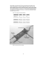
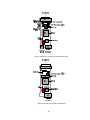
2608 Sweetgum Drive
Apex NC 27502
Toll-free: 800-549-9377
International: 919-387-0076
FAX: 919-387-1302
XS40, XSP, XS95 Board
User Manual
How to install, test, and use
your new XS Board
Copyright ©1997-1999 by X Engineering Software Systems Corporation.
All XS-prefix product designations are trademarks of XESS Corp.
All XC-prefix product designations are trademarks of Xilinx.
ABEL is a trademark of DATA I/O Corporation.
All rights reserved. No part of this publication may be reproduced, stored in a retrieval
system, or transmitted, in any form or by any means, electronic, mechanical,
photocopying, recording, or otherwise, without the prior written permission of the publisher.
Printed in the United States of America.
Limited Warranty
X Engineering Software Systems Corp. (XESS) warrants that the Product, in the course of
its normal use, will be free from defects in material and workmanship for a period of one
(1) year and will conform to XESS’s specification therefor. This limited warranty shall
commence on the date appearing on your purchase receipt.
XESS shall have no liability for any Product returned if XESS determines that the asserted
defect a) is not present, b) cannot reasonably be rectified because of damage occurring
before XESS receives the Product, or c) is attributable to misuse, improper installation,
alteration, accident or mishandling while in your possession. Subject to the limitations
specified above, your sole and exclusive warranty shall be, during the period of warranty
specified above and at XESS’s option, the repair or replacement of the product. The
foregoing warranty of XESS shall extend to repaired or replaced Products for the balance
of the applicable period of the original warranty or thirty (30) days from the date of
shipment of a repaired or replaced Product, whichever is longer.
THE FOREGOING LIMITED WARRANTY IS XESS’S SOLE WARRANTY AND IS
APPLICABLE ONLY TO PRODUCTS SOLD AS NEW. THE REMEDIES PROVIDED
HEREIN ARE IN LIEU OF a) ANY AND ALL OTHER REMEDIES AND WARRANTIES,
WHETHER EXPRESSED OR IMPLIED OR STATUTORY, INCLUDING BUT NOT
LIMITED TO, ANY IMPLIED WARRANTY OF MERCHANTABILITY OR FITNESS FOR A
PARTICULAR PURPOSE, AND b) ANY AND ALL OBLIGATIONS AND LIABILITIES OF
XESS FOR DAMAGES INCLUDING, BUT NOT LIMITED TO ACCIDENTAL,
CONSEQUENTIAL, OR SPECIAL DAMAGES, OR ANY FINANCIAL LOSS, LOST
PROFITS OR EXPENSES, OR LOST DATA ARISING OUT OF OR IN CONNECTION
WITH THE PURCHASE, USE OR PERFORMANCE OF THE PRODUCT, EVEN IF
XESS HAS BEEN ADVISED OF THE POSSIBILITY OF SUCH DAMAGES.
In the United States, some statutes do not allow exclusion or limitations of incidental or
consequential damages, so the limitations above may not apply to you. This warranty
gives you specific legal rights, and you may also have other rights which vary from state to
state.
Chapter
1
Preliminaries
Getting Help!
Here are some places to get help if you encounter problems:
n
n
If you can't get the XS Board hardware to work, send an e-mail message describing
your problem to [email protected] or check our web site at
http://www.xess.com/FPGA. Our web site also has
n
answers to frequently-asked-questions
(http://www.xess.com/FPGA/ho01000.html),
n
example designs for the XS Boards (http://www.xess.com/FPGA/ho03000.html),
n
a place to sign-up for our email forum where you can post questions to other XS
Board users (http://www.xess.com/FPGA/list_reg.html).
If you can't get your XILINX Foundation software tools installed properly, send an email message describing your problem to [email protected] or check their web site
at http://www.xilinx.com.
Take notice!!
n
The XS Boards require an external power supply to operate! They do not draw power
through the downloading cable from the PC parallel port.
n
If you are connecting a 9VDC power supply to your XS Board, please make sure the
center terminal of the plug is positive and the outer sleeve is negative.
n
The V1.3 version of the XS40 and XSP Boards now use a programmable oscillator
with a default setting of 50 MHz. You must reprogram the oscillator if you want to use
another frequency. The procedure for doing this is described on page 9. The XS95
Board uses a 12 MHz fixed-frequency oscillator and does not need to be
programmed.
Packing List
Here is what you should have received in your package:
n
an XS40, XS95 or XSP Board (note that your XSP Board will be labeled as an XS40
but the socket will contain a Xilinx Spartan FPGA with an "XCS" prefix);
n
a 6' cable with a male DB-25 connector on each end;
n
a 3.5" floppy diskette or CDROM with software utilities for using the XS40, XSP or
XS95 Board and documentation.
3
Chapter
2
Installation
Installing the XSTOOLs Utilities and Documentation
XILINX currently provides the Foundation tools for programming their FPGAs and CPLDs.
Any recent version of XILINX software should generate bitstream configuration files that
are compatible with your XS40, XSP or XS95 Boards. Follow the directions XILINX
provides for installing their software.
XESS Corp. provides the additional XSTOOLs utilities for interfacing a PC to your XS
Board. Run the SETUP.EXE program on the 3.5" diskette or CDROM to install these
utilities.
Once the XSTOOLs are installed you will see the following subdirectories:
XSTOOLS\BIN contains the executable programs for downloading to the XS Board
and for applying signals to the XS Board through the printer port. An assembler for
the microcontroller is also included.
XSTOOLS\DOCS contains the documentation and schematics for the XS40, XSP
and XS95 Boards.
Applying Power to Your XS Board
You can use your XS Board in two ways, distinguished by the method you use to apply
power to the board.
Using a 9VDC wall-mount
You can use your XS Board all by itself to experiment logic and microcontroller designs.
Just place the XS Board on a non-conducting surface as shown in Figure 1. Then apply
power to jack J9 of the XS Board from a 9V DC wall transformer with a 2.1 mm female,
center-positive plug. (See Figure 2 or Figure 3 for the location of jack J9 on your
XS40/XSP or XS95 Board, respectively.) The on-board voltage regulation circuitry will
create the voltages required by the rest of the XS Board circuitry.
Protoboard Installation
The two rows of pins from your XS Board can be plugged into a protoboard with holes
spaced at 0.1" intervals. (One of the A.C.E. protoboards from 3M is a good choice.)
4
Once plugged in, all the pins of the FPLD and microcontroller are accessible to other
circuits on the protoboard. (The numbers printed next to the rows of pins on your XS
Board correspond to the pin numbers of the FPGA or CPLD.) Power can still be supplied
to your XS Board though jack J9, or power can be applied directly through several pins on
the underside of the board. Just connect +5V, +3.3V, and ground to the following pins for
your particular type of XS Board. (You will need +3.3V only if your XS40 Board contains
an XC4000XL type of FPGA.)
• Table 1: Power supply pins for the various XS Boards.
XS Board Type
GND Pin
+5V Pin
+3.3V Pin
XS95-072 V1.2
49
78
none
XS95-108 V1.2
49
78
none
XS40-005E V1.3
52
2, 54
none
XS40-005XL V1.3
52
2
54
XS40-010E V1.3
52
2, 54
none
XS40-010XL V1.3
52
2
54
XSP-010 V1.3
52
2,54
none
• Figure 1: External connections to the XS Board.
5
• Figure 2: Arrangement of components on the XS40 and XSP Boards.
• Figure 3: Arrangement of components on the XS95 Board.
6
Connecting a PC to Your XS Board
The 6' cable included with your XS Board connects it to the parallel port of a PC. One end
of the cable attaches to the printer port and the other connects to the female DB-25
connector (J1) at the top of the XS Board as shown in Figure 1.
Connecting a VGA Monitor to Your XS Board
You can display images on a VGA monitor by connecting it to the 15-pin J2 connector at
the bottom of your XS Board (see Figure 1). You will have to download a VGA driver
circuit to your XS Board to actually display an image. You can find an example VGA driver
at www.xess.com/FPGA.
Connecting a Mouse or Keyboard to Your XS Board
You can accept inputs from a keyboard or mouse by connecting it to the J5 PS/2
connector at the bottom of your XS40 or XSP Board (see Figure 1). The XS95 Board
does not have a PS/2 connector. You will have to download a mouse or keyboard driver
circuit to your XS Board to actually display an image. You can find an example keyboard
driver at www.xess.com/FPGA..
Setting the Jumpers on Your XS Board
The default jumper settings shown in Table 2 and Table 3 configure your XS Board for use
in a logic design environment. You will need to change the jumper settings only if you are:
n
using your XS40 or XSP Board in a stand-alone mode where it is unconnected from
the PC parallel port,
n
executing microcontroller code from internal ROM instead of the external RAM on the
XS Board,
n
reprogramming the clock frequency on your XS40 or XSP Board.
The procedures for performing the operations are described in the rest of this manual.
• Table 2: Jumper settings for XS95 Board.
Jumper
Setting
Purpose
J7
1-2 (ext)
(default)
The shunt should be installed on pins 1 and 2 (ext) if the 8031 microcontroller program is stored in the
external 32 KByte RAM (U8) of the XS95 Board.
2-3 (int)
The shunt should be installed on pins 2 and 3 (int) if the program is stored internally in the
microcontroller.
7
• Table 3: Jumper settings for XS40 and XSP Boards.
Jumper
Setting
Purpose
J4
On
(default)
A shunt should be installed if you are downloading the XS40 or XSP Board through the parallel port.
Off
The shunt should be removed if the XS40 or XSP Board is being configured from the on-board serial
EEPROM (U7).
On
The shunt should be installed when the on-board serial EEPROM (U7) is being programmed.
Off
(default)
The shunt should be removed during normal board use.
1-2 (ext)
(default)
The shunt should be installed on pins 1 and 2 (ext) if the 8031 microcontroller program is stored in the
external 32 KByte RAM (U8) of the XS40 Board.
2-3 (int)
The shunt should be installed on pins 2 and 3 (int) if the program is stored internally in the
microcontroller.
On
The shunt should be installed in XS40 or XSP Boards which use the 3.3V XC4000XL type of FPGAs.
Off
The shunt should be removed on XS40 or XSP Boards which use the 5V XC4000E type of FPGAs.
On
The shunt should be installed if the XS40 or XSP Board is being configured from the on-board serial
EEPROM.
Off
(default)
The shunt should be removed if the XS40 or XSP Board is being downloaded from the PC parallel
port.
On
(default)
The shunt should be installed if the XS40 or XSP Board is being downloaded from the PC parallel port.
Off
The shunt should be removed if the XS40 or XSP Board is being configured from the on-board serial
EEPROM.
Off
(default)
The shunt should be removed during normal operations when the programmable oscillator is
generating a clock signal.
On
The shunt should be installed when the programmable oscillator frequency is being set.
J6
J7
J8
J10
J11
J12
Testing Your XS Board
Once your XS Board is installed and the jumpers are in their default configuration, you can
test the board using one of the commands listed in Table 4. You must execute the
command in a DOS window and be in the XSTOOLS\BIN directory to run the XSTEST
command.
• Table 4: Commands for testing the various types of XS Boards.
XS Board Type
Test Command
XS95-072
XSTEST XS95-072
XS95-108
XSTEST XS95-108
XS40-005E
XSTEST XS40-005E
XS40-005XL
XSTEST XS40-005XL
XS40-010E
XSTEST XS40-010E
XS40-010XL
XSTEST XS40-010XL
XSP-010
XSTEST XSP-010
8
The test procedure programs the FPGA or CPLD, loads the RAM with a test program for
the microcontroller, and then the microcontroller executes this program. The total test
period (including programming the board) is about 15 seconds for an XS40 or XSP Board,
and about a minute for an XS95 Board. If the test completes successfully, then you will
see a O displayed on the LED digit.
However, if the test program detects an error, then the LED digit displays an E or remains
blank. In this case, check the following items:
n
Make sure the board is receiving power from a 9V DC power supply through jack J9
or through the VCC and GND pins.
n
Check that the board is sitting upon a non-conducting surface and that there are no
connections to any of the pins (except for the VCC and GND pins if this is the way you
are powering the board).
n
Verify that the jumpers are in their default configuration.
n
Make sure the downloading cable is securely attached to the XS Board and the PC
parallel port.
n
Verify that the parallel port is in ECP mode. (The mode is usually set in the BIOS as
either SPP, EPP, ECP, or bidirectional. ECP mode works most reliably while
bidirectional mode is not recommended.)
If all these checks are positive, then test the board using another PC. In our experience,
99.9% of all problems are due to the parallel port. If you cannot get your XS Board to pass
the test even after taking these steps, then contact XESS Corp. to get a replacement
board.
Programming the XS Board Clock Oscillator
The XS40 and XSP Boards have a 100 MHz programmable oscillator (a Dallas
Semiconductor DS1075Z-100). The 100 MHz master frequency can be divided by factors
of 1, 2, ... up to 2048 to get clock frequencies of 100 MHz, 50 MHz, ... down to 48.8 KHz,
respectively. The divided frequency is sent to the rest of the circuitry as a clock signal.
The divisor is stored in non-volatile memory in the oscillator chip so it will resume
operation at its set frequency whenever power is applied to the board. These steps will
store a particular divisor into the oscillator chip memory:
1) In a DOS window, use the following command with arguments that list the type of XS
Board you are using and the particular clock divisor you want:
C:\> XSSETCLK XS40-005XL 8
9
This example command will set the programmable oscillator on an XS40-005XL
Board to a frequency of 100 MHz / 8 = 12.5 MHz You may use any divisor between 1
and 2048 depending upon the clock frequency you want to use.
2) The XSSETCLK will prompt you to remove the power and download cables from your
XS Board. Then you should place a shunt on jumper J12. Then re-attach the
download cable. Then reattach the power cable only after the download cable is
attached!. When power is restored to the XS Board, the programmable oscillator will
power up in its programming mode instead of generating a clock signal.
3) Press RETURN and the clock divisor will be programmed into the oscillator chip. If
you wish to change the value of the divisor, you may re-issue the XSSETCLK
command at this point with a new divisor value without having to power-down the XS
Board.
Once again, remove the power and download cables from your XS Board. Then remove
the shunt from jumper J12. Then re-attach the download cable and the power cable.
When power is restored to the XS Board, the programmable oscillator will power up in its
active mode and output a clock signal at the set frequency.
10
Chapter
3
Programming
This section will show you how to download a logic design from a PC into your XS Board,
and how to store a design in non-volatile memory on your XS Board that will become
active when power is applied.
Downloading Designs into Your XS Board
During the development and testing phases, you will usually connect the XS Board to the
parallel port of a PC and download your circuit each time you make changes to it. You
can download an FPGA design into your XS40 or XSP Board as follows:
C:\> XSLOAD CIRCUIT.BIT
where CIRCUIT.BIT is an XC4000 or Spartan bitstream file that contains the configuration
for the XC4000 or XCS FPGA. Make sure the file contains a bitstream for the type of
FPGA chip installed on your XS40 or XSP Board. This file is created using the XILINX
Foundation software tools.
You can download an XC9500-based design into the XS95 Board as follows:
C:\> XSLOAD CIRCUIT.SVF
where CIRCUIT.SVF is an XC9500 bitstream file that contains the configuration for the
XC9500 CPLD. Make sure the file contains a bitstream for the type of XC9500 chip
installed on your XS95 Board. This file is created using the XILINX Foundation software
tools.
Use one of the following commands if you need to configure the FPGA or CPLD and also
download an Intel-formatted HEX file into the static RAM of the XS Board:
C:\> XSLOAD FILE.HEX CIRCUIT.BIT
C:\> XSLOAD FILE.HEX CIRCUIT.SVF
where CIRCUIT.BIT is a bitstream file and FILE.HEX is a file containing hexadecimal data.
The HEX file could contain microcontroller object code generated by the ASM51
11
assembler, or it could be arbitrary data from some other source. Whatever its source, the
hexadecimal data is downloaded into the XS Board RAM.
XSLOAD assumes the XS Board is connected to parallel port #1 of your PC. You can
specify another port number using the -P option like so:
C:\> XSLOAD -P 2 FILE.HEX CIRCUIT.BIT
Storing Non-Volatile Designs in Your XS Board
Once your design is finished, you may want to store the design on the XS Board so that it
is configured for operation as soon as power is applied.
This is easy with the XS95 Board. The XC9500 CPLD always stores its current
configuration in an on-chip Flash memory. This configuration is restored whenever power
is applied to the XS95 Board. So your design is always available even when the board is
not connected to a PC.
But the XC4000 or XCS FPGA on the XS40 or XSP Board stores its configuration in an
on-chip RAM which is erased whenever power is interrupted. You can place an external
serial EEPROM in socket U7 which stores the FPGA configuration and reloads it on
power-up. The XILINX XC1700 series of serial EEPROMs is a good choice for this, but
you will need an external programmer to load your bitstream into the XC1700 chip. Also
the XC1700 is one-time programmable (OTP), so you will need a new chip every time you
change your logic design. Table 5 lists the serial EEPROM chips you need for storing the
bitstream files for the various types of XS Boards.
• Table 5: Recommended XILINX serial EEPROMS for various types of XS Boards.
XS Board Type
Bitstream Size
XILINX EEPROM
XS40-005E
95,008
XC17128E
XS40-005XL
151,960
XC17256E
XS40-010E
178,144
XC17256E
XS40-010XL
283,424
XC1701
95,008
XC17S10
XSP-010
You also have the option of storing your design into an AT17C256 Atmel reprogrammable
serial EEPROM if you have an XS40-005E, XS40-005XL, or XS40-010E Boards. The
XS40 Board can directly program the Atmel chip and the FPGAs on these boards have
bitstream files which are small enough to fit in the AT17C256. The following steps will
enable you to load your design into the Atmel EEPROM:
1) Turn off power to the XS Board.
2) Place a shunt on jumper J6. This enables the programming circuitry in the Atmel
EEPROM chip.
12
3) Apply power to the XS Board.
4) Use the following command to load the FPGA bitstream file into the EEPROM:
C:\> XSLOAD –SERIAL_EEPROM CIRCUIT.BIT
It will take less than a minute to program the contents of the bitstream in CIRCUIT.BIT
into the Atmel EEPROM.
5) Turn off power to the XS Board.
6) Remove the shunt on jumper J6. This disables the programming circuitry in the Atmel
EEPROM chip so your design cannot be overwritten.
Once you have your design loaded into a XILINX or Atmel EEPROM, you can place it in
socket U7 on the XS Board. Then the following steps will make the XS Board configure
itself from the EEPROM instead of the PC parallel port interface:
1) Remove the downloading cable from connector J1 of the XS Board. (As an
alternative, you can use the command ''XSPORT 0'' to make sure the upper two data
bits of the parallel port are at logic 0. These bits are connected to the mode pins of
the FPGA and must be at logic 0 or the FPGA will not power-up in the active-serial
mode.)
2) Place a shunt on jumper J10. This sets the FPGA into the active-serial mode so it will
provide a clock signal to the EEPROM which sequences the loading of the
configuration from the EEPROM into the FPGA.
3) Remove the shunts on jumpers J4 and J11. This prevents the PC interface circuitry
on the XS Board from interfering with the clock and data signals from the FPGA.
4) Apply power to the XS Board. The FPGA will be configured from the serial EEPROM.
You may reattach the downloading cable if you need to inject test signals into your
design using the XSPORT program.
13
Chapter
4
Programmer's
Models
This section discusses the organization of components on the XS Boards and introduces
the concepts required to create applications that use both the microcontroller and the
FPLD (field programmable logic device). Building FPLD-based designs is covered in
detail in the Practical Xilinx Designer by Prentice-Hall.
Microcontroller + FPLD Design Flow
The basic design flow for building microcontroller+FPLD applications is shown in Figure 4.
Initially you have to get the specifications for the system you are trying to design. Then
you have to determine what inputs are available to your system and what outputs it will
generate.
At this point, you have to partition the functions of your system between the microcontroller
and the FPLD. Some of the input signals will go to the microcontroller, some will go to the
FPLD, and some will go to both. Likewise, some of the outputs will be computed by the
microcontroller and some by the FPLD. There will also be some new intra-system inputs
and outputs created by the need for the microcontroller and the FPLD to cooperate.
In general, the FPLD will be used mainly for low-level functions where signal transitions
occur more frequently and the control logic is simpler. A specialized serial
transmitter/receiver would be a good example. Conversely, the microcontroller will be
used for higher-level functions where the responses occur less quickly and the control
logic is more complex. Reacting to commands passed in by the receiver is a good
example.Once the design has been partitioned and you have assigned the various inputs,
outputs, and functions to the microcontroller and the FPLD, then you can begin doing
detailed design of the software and hardware. For the software, you can use your favorite
editor to create a .ASM assembly-language file and assemble it with ASM51 to create a
.HEX file for the 8031 microcontroller on the XS Board. For the FPLD hardware portion,
you will enter truth-tables and logic equations into a .ABL or .VHDL file and compile it into
a .BIT or .SVF bitstream file using the XILINX Foundation software.
With the .HEX 8031-program file and the FPLD bitstream file in hand, you can download
them to the XS Board using the XSLOAD program. XSLOAD stores the contents of the
.HEX file into the static RAM on the XS Board and then it reconfigures the FPLD by
loading it with the bitstream file.
When the XS Board is loaded with the hardware and software, you need to test it to see if
it really works. The answer usually starts as "No" so you need a method of injecting test
14
signals and observing the results. XSPORT is a simple program that lets you send test
signals to the XS Board through the PC parallel port. You can trace the reaction of your
system to signals from the parallel port by programming the microcontroller and the FPLD
to output status information on the LED digit (much like placing "printf" statements in your
C language programs). This is admittedly crude but will serve if you don't have access to
programmable stimulus generators and logic analyzers.
• Figure 4: FPLD+microcontroller design flow.
XS Board Component Interconnections
The microcontroller and the FPLD on the XS Board are already connected together.
These existing connections save you the effort of having to wire them yourself, but they
also impose limitations on how your program and the FPLD hardware will interact. Highlevel views of how the microcontroller, RAM, and FPLD on the XS40, XSP, and XS95
Boards are connected are shown in Figure 5, Figure 6, and Figure 7, respectively. More
detailed schematics are presented at the end of this manual.
The oscillator output goes directly to a synchronous clock input of the FPLD. The FPLD
can control the clock it sends to the XTAL1 clock input of the microcontroller.
15
The microcontroller multiplexes the lower eight bits of a memory address with eight bits of
data and outputs this on its P0 port. Both the RAM data lines and the FPLD are
connected to P0. The RAM uses this connection to send and receive data to and from the
microcontroller. The FPLD is programmed to latch the address from P0 under control of
the ALE signal and send the latched address bits to the lower eight address lines of the
RAM.
Meanwhile, the upper eight bits of the address are output on port P2 of the microcontroller.
The RAM uses the lower seven of these address bits. The FPLD also receives the upper
eight address bits and decodes these along with the PSEN and read/write control line
(from pin P3.6 of port P3 ) from the microcontroller to generate the CE and OE signals that
enable the RAM and its output drivers, respectively. Either of the CE or OE signals can be
pulled high to disable the RAM and prevent it from having any effect on the rest of the XS
Board circuitry.
One of the outputs of the CPLD controls the reset line of the microcontroller. The
microcontroller can be prevented from having any effect on the rest of the circuitry by
forcing the RST pin high through the FPLD. (When RST is active, the microcontroller pins
are weakly pulled high.)
Many of the I/O pins of ports P1 and P3 of the microcontroller connect to the FPLD and
can be used for general-purpose I/O between the microcontroller and the FPLD. In
addition to being general-purpose I/O, the P3 pins also have special functions such as
serial transmitters, receivers, interrupt inputs, timer inputs, and external RAM read/write
control signals. If you aren't using a particular special function, then you can use the
associated pin for general-purpose I/O between the microcontroller and the FPLD. In
many cases, however, you will program the FPLD to make use of the special-purpose
microcontroller pins. (For example, the FPLD could generate microcontroller interrupts.) If
you want to use the special-purpose pin with an external circuit, then the FPLD I/O pin
connected to it must be tristated.
An LED digit connects directly to the FPLD. (These same FPLD pins also drive the VGA
monitor connector. The FPLD can be programmed so the microcontroller can control the
LEDs either through P1 or P3 or by memory-mapping a latch for the LED into the memory
space of the 8031.
The PC can transmit signals to the XS Board through the eight data output bits of the
printer port. The FPLD has direct access to these signals. The microcontroller can also
access them if you program the FPLD to pass the data bits onto the FPLD I/O pins
connected to the microcontroller.
Communication from the XS Board back to the PC also occurs through the parallel port.
The parallel port status pins are connected to pins of microcontroller ports P1 and P3 .
Either the microcontroller or the FPLD can drive the status pins. The PC can read the
status pins to fetch data from the XS Board.
The FPGAs on the XS40 and XSP Boards also have access to the clock and data lines of
a keyboard or mouse attached to the PS/2 port of the board.
16
• Table 6: XS40 Board pin descriptions.
XS40 Pin
Connects to…
Description
25
26
24
20
23
18
19
13
44
45
46
47
48
49
32
34
37
36
29
14
7
8
9
6
77
70
66
67
69
68
62
27
41
40
39
38
35
81
80
10
59
57
51
56
50
58
60
28
3
4
5
78
79
82
83
84
61
65
75
S0, BLUE0
S1, BLUE1
S2, GREEN0
S3, GREEN1
S4, RED0
S5, RED1
S6, HSYNCB
CLK
PC_D0
PC_D1
PC_D2
PC_D3
PC_D4
PC_D5
PC_D6
PC_D7
XTAL1
RST
ALEB
PSENB
P1.0
P1.1
P1.2
P1.3
P1.4, PC_S4
P1.5, PC_S3
P1.6, PC_S5
P1.7, VSYNCB
P3.1(TXD), PC_S6,
P3.4(T0),PS/2 CLK
P3.6(WRB), WEB
P3.7(RDB)
P0.0(AD0), D0
P0.1(AD1), D1
P0.2(AD2), D2
P0.3(AD3), D3
P0.4(AD4), D4
P0.5(AD5), D5
P0.6(AD6), D6
P0.7(AD7), D7
P2.0(A8), A8
P2.0(A9), A9
P2.0(A10), A10
P2.0(A11), A11
P2.0(A12), A12
P2.0(A13), A13
P2.0(A14), A14
P2.0(A15)
A0
A1
A2
A3
A4
A5
A6
A7
OEB
CEB
PC_S7
These pins drive the individual segments of the LED display (S0-S6 and DP). They
also drive the color and horizontal sync signals for a VGA monitor.
An input driven by the 100 MHz programmable oscillator.
These pins are driven by the data output pins of the PC parallel port. Clocking signals
can only be reliably applied through pins 44 and 45 since these have additional
hysterisis circuitry. Pins 32 and 34 are mode signals for the FPGA so you must adjust
your design to account for the way that the Foundation tools handle these pins.
Pin that drives the uC clock input
Pin that drives the uC reset input
Pin that monitors the uC address latch enable
Pin that monitors the uC program store enable
These pins connect to the pins of Port 1 of the uC. Some of the pins are also
connected to the status input pins of the PC parallel port. Pin 67 drives the vertical
sync signal for a VGA monitor.
These pins connect to some of the pins of Port 3 of the uC. The uC has specialized
functions for each of the port pins indicated in parentheses. Pin 62 connects to the
data write pin of the uC and the write-enable pin of the RAM. Pin 69 connects to a
status input pin of the PC parallel port and the PS/2 data line. Pin 68 connects to the
These pins connect to Port 0 of the uC which is also a multiplexed address/data port.
These pins also connect to the data pins of the RAM.
These pins connect to Port 2 of the uC which also outputs the upper address byte.
These pins also connect to the 7 upper address bits of the RAM.
These pins drive the 8 lower address bits of the RAM.
Pin that drives the RAM output enable.
Pin that drives the RAM chip enable.
Pin that drives a status input pin of the PC parallel port.
17
• Figure 5: XS40 Board programmer's model.
18
• Table 7: XSP Board pin descriptions.
XS40 Pin
Connects to…
Description
25
26
24
20
23
18
19
13
44
45
46
47
48
49
37
36
29
14
7
8
9
6
77
70
66
67
S0, BLUE0
S1, BLUE1
S2, GREEN0
S3, GREEN1
S4, RED0
S5, RED1
S6, HSYNCB
CLK
PC_D0
PC_D1
PC_D2
PC_D3
PC_D4
PC_D5
XTAL1
RST
ALEB
PSENB
P1.0
P1.1
P1.2
P1.3
P1.4, PC_S4
P1.5, PC_S3
P1.6, PC_S5
P1.7, VSYNCB
P3.1(TXD), PC_S6,
PS/2 DATA
These pins drive the individual segments of the LED display (S0-S6 and DP). They
also drive the color and horizontal sync signals for a VGA monitor.
69
68
62
27
41
40
39
38
35
81
80
10
59
57
51
56
50
58
60
28
3
4
5
78
79
82
83
84
61
65
75
P3.4(T0),PS/2 CLK
P3.6(WRB), WEB
P3.7(RDB)
P0.0(AD0), D0
P0.1(AD1), D1
P0.2(AD2), D2
P0.3(AD3), D3
P0.4(AD4), D4
P0.5(AD5), D5
P0.6(AD6), D6
P0.7(AD7), D7
P2.0(A8), A8
P2.0(A9), A9
P2.0(A10), A10
P2.0(A11), A11
P2.0(A12), A12
P2.0(A13), A13
P2.0(A14), A14
P2.0(A15)
A0
A1
A2
A3
A4
A5
A6
A7
OEB
CEB
PC_S7
An input driven by the 100 MHz programmable oscillator.
These pins are driven by the data output pins of the PC parallel port. Clocking signals
can only be reliably applied through pins 44 and 45 since these have additional
hysterisis circuitry.
Pin that drives the uC clock input
Pin that drives the uC reset input
Pin that monitors the uC address latch enable
Pin that monitors the uC program store enable
These pins connect to the pins of Port 1 of the uC. Some of the pins are also
connected to the status input pins of the PC parallel port. Pin 67 drives the vertical
sync signal for a VGA monitor.
These pins connect to some of the pins of Port 3 of the uC. The uC has specialized
functions for each of the port pins indicated in parentheses. Pin 62 connects to the
data write pin of the uC and the write-enable pin of the RAM. Pin 69 connects to a
status input pin of the PC parallel port and the PS/2 data line. Pin 68 connects to the
PS/2 clock line.
These pins connect to Port 0 of the uC which is also a multiplexed address/data port.
These pins also connect to the data pins of the RAM.
These pins connect to Port 2 of the uC which also outputs the upper address byte.
These pins also connect to the 7 upper address bits of the RAM.
These pins drive the 8 lower address bits of the RAM.
Pin that drives the RAM output enable.
Pin that drives the RAM chip enable.
Pin that drives a status input pin of the PC parallel port.
19
• Figure 6: XSP Board programmer's model.
20
• Table 8: XS95 Board pin descriptions.
XS95 Pin
21
23
19
17
18
14
15
24
9
46
47
48
50
51
52
81
80
10
45
20
13
6
7
11
5
72
71
66
67
31
70
69
68
26
33
63
32
44
43
41
40
39
37
36
35
58
56
54
55
53
57
61
34
75
79
82
84
1
3
83
2
62
65
4
12
25
74
Connects to…
S0,BLUE0
S1,BLUE1
S2,GREEN0
S3,GREEN1
S4,RED0
S5,RED1
S6,HSYNCB
DP,VSYNCB
CLK
PC_D0
PC_D1
PC_D2
PC_D3
PC_D4
PC_D5
PC_D6
PC_D7
XTAL1
RST
ALEB
PSENB
P1.0
P1.1
P1.2
P1.3
P1.4,PC_S4
P1.5,PC_S3
P1.6,PC_S5
P1.7
P3.0(RXD)
P3.1(TXD), PC_S6
P3.2(INTB0)
P3.3(INTB1)
P3.4(T0)
P3.5(T1)
P3.6(WRB), WEB
P3.7(RDB)
P0.0(AD0), D0
P0.1(AD1), D1
P0.2(AD2), D2
P0.3(AD3), D3
P0.4(AD4), D4
P0.5(AD5), D5
P0.6(AD6), D6
P0.7(AD7), D7
P2.0(A8), A8
P2.0(A9), A9
P2.0(A10), A10
P2.0(A11), A11
P2.0(A12), A12
P2.0(A13), A13
P2.0(A14), A14
P2.0(A15)
A0
A1
A2
A3
A4
A5
A6
A7
OEB
CEB
FREE0
FREE1
FREE2
FREE3
Description
These pins drive the individual segments of the LED display (S0-S6 and DP). They also drive
the color, horizontal, and vertical sync signals for a VGA monitor.
An input driven by the 12 MHz oscillator.
These pins are driven by the data output pins of the PC parallel port. Clocking signals can only
be reliably applied through pins 46 and 47 since these have additional hysterisis circuitry.
Pin that drives the uC clock input
Pin that drives the uC reset input
Pin that monitors the uC address latch enable
Pin that monitors the uC program store enable
These pins connect to the pins of Port 1 of the uC. Some of the pins are also connected to the
status input pins of the PC parallel port.
These pins connect to the pins of Port 3 of the uC. The uC has specialized functions for each of
the port pins indicated in parentheses. Pin 63 connects to the data write pin of the uC and the
write-enable pin of the RAM. Pin 70 connects to a status input pin of the PC parallel port.
These pins connect to Port 0 of the uC which is also a multiplexed address/data port. These
pins also connect to the data pins of the RAM.
These pins connect to Port 2 of the uC which also outputs the upper address byte. These pins
also connect to the 7 upper address bits of the RAM.
These pins drive the 8 lower address bits of the RAM.
Pin that drives the RAM output enable.
Pin that drives the RAM chip enable.
These pins are not connected to other devices and can be used as general purpose I/O.
21
76
77
FREE4
FREE5
22
• Figure 7: XS95 Board programmer's model.
23
XS40 and XSP Board Schematic
XS95 Board Schematic